WO2023224024A1 - ロジックアナライザ回路、集積回路および集積回路システム - Google Patents
ロジックアナライザ回路、集積回路および集積回路システム Download PDFInfo
- Publication number
- WO2023224024A1 WO2023224024A1 PCT/JP2023/018224 JP2023018224W WO2023224024A1 WO 2023224024 A1 WO2023224024 A1 WO 2023224024A1 JP 2023018224 W JP2023018224 W JP 2023018224W WO 2023224024 A1 WO2023224024 A1 WO 2023224024A1
- Authority
- WO
- WIPO (PCT)
- Prior art keywords
- data
- circuit
- logic analyzer
- compression
- observation target
- Prior art date
- Legal status (The legal status is an assumption and is not a legal conclusion. Google has not performed a legal analysis and makes no representation as to the accuracy of the status listed.)
- Ceased
Links
Images








Classifications
-
- G—PHYSICS
- G01—MEASURING; TESTING
- G01R—MEASURING ELECTRIC VARIABLES; MEASURING MAGNETIC VARIABLES
- G01R31/00—Arrangements for testing electric properties; Arrangements for locating electric faults; Arrangements for electrical testing characterised by what is being tested not provided for elsewhere
- G01R31/28—Testing of electronic circuits, e.g. by signal tracer
- G01R31/317—Testing of digital circuits
- G01R31/3177—Testing of logic operation, e.g. by logic analysers
-
- G—PHYSICS
- G06—COMPUTING OR CALCULATING; COUNTING
- G06F—ELECTRIC DIGITAL DATA PROCESSING
- G06F11/00—Error detection; Error correction; Monitoring
- G06F11/30—Monitoring
- G06F11/34—Recording or statistical evaluation of computer activity, e.g. of down time, of input/output operation ; Recording or statistical evaluation of user activity, e.g. usability assessment
- G06F11/3466—Performance evaluation by tracing or monitoring
- G06F11/3476—Data logging
-
- G—PHYSICS
- G01—MEASURING; TESTING
- G01R—MEASURING ELECTRIC VARIABLES; MEASURING MAGNETIC VARIABLES
- G01R31/00—Arrangements for testing electric properties; Arrangements for locating electric faults; Arrangements for electrical testing characterised by what is being tested not provided for elsewhere
- G01R31/28—Testing of electronic circuits, e.g. by signal tracer
-
- G—PHYSICS
- G06—COMPUTING OR CALCULATING; COUNTING
- G06F—ELECTRIC DIGITAL DATA PROCESSING
- G06F11/00—Error detection; Error correction; Monitoring
- G06F11/30—Monitoring
- G06F11/32—Monitoring with visual or acoustical indication of the functioning of the machine
- G06F11/321—Display for diagnostics, e.g. diagnostic result display, self-test user interface
- G06F11/322—Display of waveforms, e.g. of logic analysers
-
- G—PHYSICS
- G06—COMPUTING OR CALCULATING; COUNTING
- G06F—ELECTRIC DIGITAL DATA PROCESSING
- G06F11/00—Error detection; Error correction; Monitoring
- G06F11/30—Monitoring
- G06F11/34—Recording or statistical evaluation of computer activity, e.g. of down time, of input/output operation ; Recording or statistical evaluation of user activity, e.g. usability assessment
- G06F11/3466—Performance evaluation by tracing or monitoring
- G06F11/348—Circuit details, i.e. tracer hardware
-
- H—ELECTRICITY
- H03—ELECTRONIC CIRCUITRY
- H03M—CODING; DECODING; CODE CONVERSION IN GENERAL
- H03M7/00—Conversion of a code where information is represented by a given sequence or number of digits to a code where the same, similar or subset of information is represented by a different sequence or number of digits
- H03M7/30—Compression; Expansion; Suppression of unnecessary data, e.g. redundancy reduction
-
- H—ELECTRICITY
- H03—ELECTRONIC CIRCUITRY
- H03M—CODING; DECODING; CODE CONVERSION IN GENERAL
- H03M7/00—Conversion of a code where information is represented by a given sequence or number of digits to a code where the same, similar or subset of information is represented by a different sequence or number of digits
- H03M7/30—Compression; Expansion; Suppression of unnecessary data, e.g. redundancy reduction
- H03M7/40—Conversion to or from variable length codes, e.g. Shannon-Fano code, Huffman code, Morse code
-
- H—ELECTRICITY
- H03—ELECTRONIC CIRCUITRY
- H03M—CODING; DECODING; CODE CONVERSION IN GENERAL
- H03M7/00—Conversion of a code where information is represented by a given sequence or number of digits to a code where the same, similar or subset of information is represented by a different sequence or number of digits
- H03M7/30—Compression; Expansion; Suppression of unnecessary data, e.g. redundancy reduction
- H03M7/46—Conversion to or from run-length codes, i.e. by representing the number of consecutive digits, or groups of digits, of the same kind by a code word and a digit indicative of that kind
Definitions
- TECHNICAL FIELD This disclosure relates to integrated circuits, and more particularly to logic analyzer circuits that monitor signals within integrated circuits.
- a monitoring circuit is installed to acquire the desired signal of the user circuit, and a mechanism is provided to acquire the internal signal and output it to the outside. This monitoring circuit is called a logic analyzer circuit.
- this logic analyzer circuit By making this logic analyzer circuit a logic-synthesizable circuit that does not depend on the device on which it is mounted, it becomes possible to implement and verify it together with a user circuit block without relying on ASIC or FPGA (for example, see Patent Document 1).
- a user circuit and a logic analyzer circuit to be monitored are implemented in an integrated circuit, and state changes of the monitored signals are recorded along with time stamps.
- the data size of the acquired signal is reduced by sampling only state changes instead of continuously sampling the value of the probe target signal according to the system clock.
- an encoding format using ASCII American Standard Code for Information Interchange
- VCD Value Change Dump
- a program-enabled processor inside the integrated circuit reads the file, converts it into a waveform, and outputs it to a display or the like via a video output port in real time.
- the present disclosure has been made to solve the above-mentioned problems, and aims to provide a logic analyzer circuit, an integrated circuit, and an integrated circuit system that can reduce the data size of signals to be monitored. shall be.
- a logic analyzer circuit includes a trace capture circuit that acquires the N observation target signals when at least one of the N observation target signals from the observation target circuit changes, and a trace capture circuit. and a buffer for storing the signal data acquired by.
- the signal data includes an M-bit wide timestamp indicating the acquired time, and N-bit wide state change data corresponding to each value of the N observation target signals.
- the signal data is fixed length binary format data of (M+N) bits.
- the logic analyzer circuit, integrated circuit, and integrated circuit system of the present disclosure can reduce the data size of a signal to be monitored.
- FIG. 1 is a schematic diagram of an integrated circuit 1 based on Embodiment 1.
- FIG. 3 is a diagram illustrating a format of signal data stored in a buffer 105 based on the first embodiment.
- FIG. 2 is a diagram illustrating an example of the configuration of an external system 109 connected to the integrated circuit 1 based on the first embodiment.
- FIG. 3 is a diagram illustrating details of a signal data set stored in a buffer 105 based on the first embodiment.
- FIG. FIG. 3 is a diagram illustrating a conventional signal data acquisition format as a comparative example.
- FIG. 3 is a diagram illustrating a data size according to a method according to the first embodiment and a data size according to a method according to a comparative example.
- FIG. 2 is a schematic diagram of integrated circuit 1# based on Embodiment 2.
- FIG. FIG. 3 is an image diagram of division of a plurality of signal data sets.
- 7 is a flow diagram illustrating a process of compressing blocks of multiple patterns in a compression circuit 606 according to the second embodiment.
- FIG. FIG. 7 is a diagram illustrating the data size of the method according to the second embodiment and the data size of the method according to the comparative example.
- 7 is a diagram illustrating an internal configuration of a compression circuit 606 based on Embodiment 3.
- FIG. FIG. 6 is a schematic diagram illustrating a scanning method of an input data scanning unit 1101 in each block of divided signal data.
- 12 is a flow diagram illustrating compression processing of each block in compression circuit 606 according to Embodiment 3.
- FIG. 7 is a diagram illustrating a case where compression processing is performed in parallel according to the third embodiment.
- FIG. 3 is a timing chart diagram broadly showing compression code generation processing for a plurality of blocks.
- FIG. 2 is a schematic diagram illustrating a Huffman table update processing method in a Huffman table update phase. A specific example of a Huffman table according to the third embodiment is shown.
- FIG. 7 is a diagram illustrating an integrated circuit according to another embodiment.
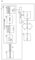
- FIG. 1 is a schematic diagram of an integrated circuit 1 based on the first embodiment.
- an integrated circuit 1 includes an observation target circuit 101, a logic analyzer circuit 103 that monitors an observation target signal 102 of the observation target circuit 101, a processor bus 108, and a processor 107 capable of executing a program. include.
- Logic analyzer circuit 103 includes a trace capture circuit 104 and a buffer 105.
- the trace capture circuit 104 acquires a signal when a change occurs in the observation target signal 102.
- Buffer 105 temporarily stores the acquired signal data.
- the processor 107 acquires the signal data temporarily stored in the buffer 105 via the processor bus 108. Further, the processor 107 sends the data to the external system 109 via the external bus 110.
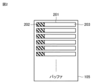
- FIG. 2 is a diagram illustrating the format of signal data stored in the buffer 105 according to the first embodiment.
- the trace capture circuit 104 acquires a signal when the observation target signal 102 changes.
- Buffer 105 stores one signal data set 201 acquired by trace capture circuit 104.
- the signal data set 201 has a timestamp 202 located at the beginning and state change data 203. Note that the timestamp 202 may have any bit width as long as it is possible to measure the time until the next change in the observation target signal 102.
- the timestamp 202 overflows, the timestamp 202 and state change data 203 at the time of overflow are recorded even if there is no signal change, to clearly indicate that an overflow has occurred.
- the state change data 203 may be assigned a bit width necessary to include the desired observation target signal.
- the signal data set 201 in this example combines a timestamp 202 and state change data 203 into a fixed-length binary format.
- the buffer 105 stores a plurality of signal data in the order of the oldest signal data set 201 from the top.
- FIG. 3 is a diagram illustrating an example of the configuration of the external system 109 connected to the integrated circuit 1 based on the first embodiment.
- external system 109 includes a debugger 2, a PC (Personal Computer) 3, and a display 5.
- Signal data sent from the integrated circuit 1 is input to the debugger 2 via an external bus 110 connected to the integrated circuit 1.
- the debugger 2 changes the data format of the signal data to a format compatible with the bus that the PC 3 has, and transmits it to the PC 3.
- the PC 3 has software for displaying the signal data on the display 5, and uses the software to decode the signal data according to a predetermined procedure, reconstruct it into a waveform, and display it on the display 5.
- FIG. 4 is a diagram illustrating details of the signal data set stored in the buffer 105 based on the first embodiment.
- a timestamp 202 indicating the data acquisition time is placed on the MSB (Most Significant Bit) side.
- 8 bits are allocated to the timestamp 202.
- the monitored signal 502 consisting of 120 signals is treated as 1-bit binary data for each signal, and these 120 signals are combined from the MSB (Most Significant Bit) side to the LSB (Least Significant Bit) side. By doing so, 120-bit state change data 203 is generated.
- One signal data is 128-bit fixed-length binary data that is a combination of an 8-bit timestamp 202 and 120-bit state change data 203.
- the size of the signal data will always be a fixed length of 128 bits (16 bytes) and will never exceed this.
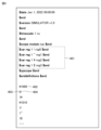
- FIG. 5 is a diagram illustrating a conventional signal data acquisition format as a comparative example. Referring to FIG. 5, a signal data acquisition format when using the VCD format will be described. In the VCD format, character string definitions 401 that correspond to all signals to be monitored are placed at the beginning of the file.
- the time stamp 402 is followed by a value 403 after the change of the signal whose state has changed, one line after the other.
- This is a format in which the corresponding signal identification character string 404 is recorded.
- the data size per time stamp is 2+Nd+3 ⁇ Nc bytes.
- the data size increases in proportion to the number of changed signals.
- the number of signals to be monitored is large, for example, the number of signals Nc is 120.
- FIG. 6 is a diagram illustrating the data size according to the method according to the first embodiment and the data size according to the method according to the comparative example.
- this example shows the data size for the number of state change signals per timestamp of signal data when the VCD format is used.
- Nd 4 as the data size of the time stamp.
- the data size for the number of state change signals per time stamp of signal data remains constant even when the number of signals increases.
- the data size can be significantly reduced even when a large number of state change signals are generated per time stamp.
- FIG. 7 is a schematic diagram of integrated circuit 1# based on the second embodiment.
- integrated circuit 1# differs from integrated circuit 1 in that it is replaced with logic analyzer circuit 603#.
- the rest of the configuration is the same as that described with reference to FIG. 1, so detailed description thereof will not be repeated.
- Logic analyzer circuit 603# further includes a compression circuit 606 compared to logic analyzer circuit 103.
- the compression circuit 606 reads out the data group (a plurality of signal data sets) stored in the buffer 105 and compresses it.
- the compression algorithm may be a run-length method to compress into a predetermined binary format.
- each value of the observed signal at the start of signal acquisition is used as a header, and then the number of times the signal has the same value continuously in the time axis direction is listed for each change in signal value.
- Possible formats are possible. When this compression algorithm is applied, a high compression ratio can be obtained when the frequency of signal changes is low.
- the data group may be divided into multiple blocks and a compression algorithm may be applied to each block.
- the number of blocks to be divided may be changed to compress multiple patterns of blocks, and compression with a smaller data size may be selected.
- FIG. 8 is an image diagram of division of a plurality of signal data sets. Referring to FIG. 8(A), it is an image diagram when dividing in the data arrangement direction.
- FIG. 8(B) it is an image diagram when data is further divided in the time direction.
- FIG. 9 is a flow diagram illustrating the process of compressing multiple patterns of blocks in the compression circuit 606 according to the second embodiment.
- compression circuit 606 acquires signal data from buffer 105 and determines whether the signal data has been acquired to a predetermined size (step S1).
- the compression circuit 606 waits until the signal data can be acquired up to a predetermined size (NO in step S1), and if it is determined that the signal data can be acquired up to the predetermined size (YES in step S1), ), the signal data set is divided into N blocks in the direction of data arrangement (step S2).
- the compression circuit 606 performs a predetermined compression process on the divided N blocks of data (step S3).
- the compression circuit 606 determines whether compression processing for all N divided blocks has been completed (step S4).
- the compression circuit 606 repeats the predetermined compression process of step S3 until the compression process for all N divided blocks is completed, and when the compression process is completed, the process proceeds to the next step.
- the compression circuit 606 further divides each of the N blocks into two (step S5). Specifically, it is further divided in the time direction as explained with reference to FIG. 8(B).
- the compression circuit 606 performs a predetermined compression process on the divided 2N blocks of data (step S6).
- the compression circuit 606 determines whether compression processing for all 2N divided blocks has been completed (step S7).
- the compression circuit 606 repeats the predetermined compression process of step S6 until the compression process for all 2N divided blocks is completed, and when the compression process is completed, the process proceeds to the next step.
- the compression circuit 606 further divides each of the N blocks into four (step S8). Specifically, it is further divided into two in the time direction using a method similar to that described with reference to FIG. 8(B).
- the compression circuit 606 performs a predetermined compression process on the divided 4N blocks of data (step S9).
- the compression circuit 606 determines whether the compression processing for all 4N divided blocks has been completed (step S10).
- the compression circuit 606 repeats the predetermined compression process of step S6 until the compression process for all 4N divided blocks is completed, and when the compression process is completed, the process proceeds to the next step.
- the compression circuit 606 selects uncompressed data and the method with the smallest data size among the three types of compression methods (step S11).
- the compression circuit 606 then ends the process (END). According to the above method, data of the method with the smallest data size among the plurality of compression patterns is selected, and the selected data is sent to the processor 107.
- the predetermined compression processing algorithm may be a widely used reversible compression algorithm such as ZIP or GZIP, or any other reversible compression algorithm that is easy to implement in an integrated circuit. may also be used.
- FIG. 10 is a diagram illustrating the data size of the method according to the second embodiment and the data size of the method according to the comparative example.
- a graph of the data size versus the number of state change signals per time stamp is shown when compression processing is performed for each 128 data set using the run-length format.
- the data size can be reduced to 40% or less, so it is possible to reduce the data size compared to the VCD format.
- Embodiment 3 below, a case will be described in which Huffman codes are used as the compression algorithm.
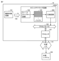
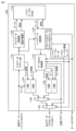
- FIG. 11 is a diagram illustrating the internal configuration of compression circuit 606 based on the third embodiment.
- the compression circuit 606 includes an input data scan unit 1101, an original data SRAM (Static Random Access Memory) 1102, a compressed data SRAM 1106, a write data control unit 1104, a Huffman table SRAM 1103, and a read data It includes a control section 1105, a data output control section 1107, and selectors 1108 and 1109.
- the original data SRAM 1102 temporarily stores one block of signal data from the buffer 105 before compression, and has a two-sided bank configuration with an A side and a B side. Switch and use.
- the Huffman table SRAM 1103 stores a Huffman table.
- the write data control unit 1104 creates statistical information such as a decision tree or a histogram from the signal data to be compressed, and updates a Huffman table.
- the read data control unit 1105 reads the compression code from the Huffman table SRAM 1103 based on the signal data to be compressed, and outputs the Huffman table data to the processor bus 108 when updating the Huffman table.
- the compressed data SRAM 1106 stores compressed codes, has a two-sided bank configuration of A side and B side, and is used by switching the bank sides according to the processing pipeline stage described later.
- the data output control unit 1107 calculates the amount of compressed data for one block and determines output data.
- the selector 1108 selects data to be output to the processor bus 108 between the original data SRAM 1102 and the compressed data SRAM 1106.
- the selector 1109 selects data to be output to the processor bus 108 between the output of the selector 1108 and the Huffman table data.
- division method does not need to be limited to 8-bit units, and division may be performed in units of 4 bits, 16 bits, or other bit numbers.
- FIG. 12 is a schematic diagram illustrating a scanning method of the input data scanning unit 1101 in each block of divided signal data.
- each block has an 8-bit data array of L rows in the time axis direction.
- the input data scanning unit 1101 sequentially imports 8 bits each in L times from top (old data) to bottom (new data) in the time axis direction and executes compression processing.
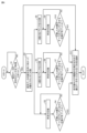
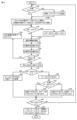
- FIG. 13 is a flow diagram illustrating compression processing of each block in compression circuit 606 according to the third embodiment.
- the input data scanning unit 1101 determines whether this block is the first block of the data to be compressed (step S20).
- Step S22 if the input data scanning unit 1101 determines that it is the first block (YES in step S20), it instructs the write data control unit 1104 to store an initial Huffman table in the Huffman table SRAM 1103. (Step S22).
- step S20 determines that it is not the first block (NO in step S20)
- step S24 the input data scanning unit 1101 starts scanning one block of signal data and stores the uncompressed signal data in the original data SRAM 1102.
- the input data scanning unit 1101 determines whether all 8 bits of the scanned data are 0 (step S26).
- step S26 If the input data scanning unit 1101 determines that all 8 bits are 0 (YES in step S26), it adds +1 to the built-in 0 data counter for the read data control unit 1105 (step S28).
- step S26 determines that all 8 bits are not 0 (NO in step S26)
- step S30 the write data control unit 1104 updates statistical information such as a histogram based on the scanned 8-bit data.
- the read data control unit 1105 performs read access using the 8-bit data scanned from the Huffman table SRAM 1103 as an address, and reads out the compressed code (step S32).
- the data output control unit 1107 packs and writes the compressed code output from the read data control unit 1105 into the compressed data SRAM 1106 (step S34).
- the input data scanning unit 1101 determines whether scanning of the signal data of 8 bits each has been completed L times (step S36).
- step S36 If the input data scanning unit 1101 determines that the scanning of the signal data in 8-bit units has not been completed L times (NO in step S36), the process advances to step S54, and the input data scanning unit 1101 scans the signal data for the next 8 bits. Scan an ordered 8-bit data array. Then, the process advances to step S26.
- the input data scanning unit 1101 determines that the scanning of signal data of 8 bits each has been completed L times (YES in step S36)
- the input data scanning unit 1101 scans the two bank surfaces (A/B) of the original data SRAM 1102 and the compressed data SRAM 1106. ) between the write side and the read side, and the block counter built in the read data control unit 1105 is incremented by +1 (step S37).
- the read data control unit 1105 determines whether the value of the built-in 0 data counter matches L (step S38).
- the read data control unit 1105 determines that the value of the 0 data counter matches L (YES in step S38), it outputs the all 0 flag as ON (“1”).
- the read data control unit 1105 instructs the data output control unit 1107 to discard one block of compressed data stored in the compressed data SRAM 1106 (step S52). Then, the process advances to the next step S48.
- the read data control unit 1105 determines that the value of the built-in 0 data counter does not match L (NO in step S38), it outputs the all 0 flag as OFF (“0”) (step S40). ).
- the data output control unit 1107 determines whether the size of one block of compressed data stored in the compressed data SRAM 1106 is larger than or equal to the size of the signal data before compression (8 ⁇ L bits). (Step S42).
- the data output control unit 1107 outputs the compression flag as OFF (“0”). do. Accordingly, data on the original data SRAM 1102 side is selected according to the selector 1108, and then output to the processor bus 108 (step S46).
- the data output control unit 1107 sets the compression flag. Output as ON (“1”). Accordingly, data on the compressed data SRAM 1106 side is selected according to the selector 1108, and then output to the processor bus 108 (step S44).
- the write data control unit 1104 performs a process based on statistical information such as a calculated histogram. , updates the Huffman table information stored in the Huffman table SRAM 1103, outputs the Huffman table data to the processor bus 108 via the selector 1109, and resets the block counter to 0 (step S50).
- step S48 if the value of the block counter has not reached P times (NO in step S48), the process returns to step S20 and the above process is repeated. As a result, compression processing is repeatedly executed for each block.
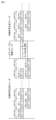
- FIG. 14 is a diagram illustrating a case where compression processing according to the third embodiment is performed in parallel.
- FIG. 14 a case is shown here in which the process is divided into two pipeline stages for speeding up. Specifically, a timing chart is shown when consecutive blocks are processed in parallel.
- stage 1 compression code generation processing is performed on the Mth block.
- L pieces of 8-bit data of signal data D-1 to DL (L corresponds to the number of scan lines shown in FIG. 12) are input in accordance with the clock cycle.
- Reading of the last compressed code is completed in the L+1th cycle of phase M.
- bank switching is performed, in the next cycle (L+3 cycle), all 0 determination is performed, and in the next cycle (L+4 cycle), compressed data size determination is performed. .
- stage 1 compression code generation processing is performed on the M+1st block
- stage 2 data output processing is performed on the Mth block.
- stage 2 a process is executed during L+4 cycles to output compressed data or original data to the processor bus 108 based on the determination result, or to output no data at all based on an all-0 determination.
- FIG. 15 is a timing chart diagram broadly showing compression code generation processing for multiple blocks.
- the Huffman table information is updated and output to the processor bus 108.
- the stage 1 compression code generation and stage 2 data output processing are repeated for the M+Pth block to the M+(2P-1)th block (ie, P blocks).
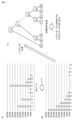
- FIG. 16 is a schematic diagram illustrating a Huffman table update processing method in the Huffman table update phase.
- the Huffman table update phase begins, and the number of votes for each of the 256 nodes is divided by the total number of votes L x P, and converted to the probability of occurrence (%). be done.
- the events are sorted in descending order of probability of occurrence.
- a Huffman tree is generated based on the sorted data, and a compression code is generated for each node.
- the generated compressed code is written to the Huffman table SRAM 1103 using the original data corresponding to the corresponding node as an address, and is also output to the processor bus 108 in order to decompress the compressed data on the external system side or the processor side. .
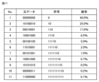
- FIG. 17 shows a specific example of the Huffman table according to the third embodiment.
- the left column shows the original 8-bit data
- the right column shows its appearance probability.
- a case is shown in which 11 types of 8-bit data exist within a predetermined block to be compressed.
- the center column is a Huffman code derived by calculating a decision tree based on each appearance probability. Codes are assigned as 0, 10, 110, . . . in descending order of appearance probability.
- the code compression rate when using a Huffman table is expressed by the following formula, where the i-th code size is S i (bit) and the i-th appearance probability is P i (%).
- N is the total number of types of 8-bit data that appear.
- the compression ratio in the case of the Huffman table shown in FIG. 17 is calculated as follows using the above formula.
- the Huffman table SRAM 1103 that stores the Huffman table only needs to secure at most 256 addresses, and can be implemented in a small area as an SRAM on an LSI without needing to be placed on an external memory.
- the Huffman table in the built-in SRAM of the LSI cycle-based reference is possible, and compared to implementing the Huffman table in external memory such as DRAM, access latency is lower and faster Huffman encoding is performed. becomes possible.
- FIG. 18 is a diagram illustrating an integrated circuit according to another embodiment.
- integrated circuit 2 differs from integrated circuit 1# in that a second buffer 1801 is added.
- the rest of the configuration is the same as that described with reference to FIG. 7, so detailed description thereof will not be repeated.
- logic analyzer circuit 1802 Compared to logic analyzer circuit 603#, logic analyzer circuit 1802 further includes a second buffer 1801 that temporarily holds compressed data.
- the compression circuit 606 reads the data group (a plurality of signal data sets) stored in the buffer 105# at an earlier timing, and stores the compressed data in the second buffer 1801 before a read request is issued from the processor. Therefore, when compared with the logic analyzer circuit 603#, the size of the buffer 105# can be made smaller, and since the second buffer 1801 stores compressed data, the size of the second buffer 1801 can also be made smaller. , the total size of the buffer 105# and the second buffer 1801 can be smaller than the size of the buffer 105 of the logic analyzer circuit 603#, and it is possible to improve the efficiency of the memory size used for the buffer. be.
- the data compressed by the compression circuit 606 is decompressed by the processor 107 built into the integrated circuit 2, converted into a general-purpose data format such as VCD (Value Change Dump), and sent via the external bus 110. It may also be supplied to an external system 109. According to such a system, it is possible to reduce the amount of data transferred on the processor bus and to supply data in a general-purpose data format to an external system.
- VCD Value Change Dump
- the configuration exemplified as the embodiment described above is an example of the configuration of the present disclosure, and it is possible to combine it with another known technology, or omit some parts without departing from the gist of the present disclosure. , it is also possible to change the configuration. Further, in the embodiment described above, the processes and configurations described in other embodiments may be appropriately adopted and implemented.
Landscapes
- Engineering & Computer Science (AREA)
- Theoretical Computer Science (AREA)
- General Engineering & Computer Science (AREA)
- Physics & Mathematics (AREA)
- General Physics & Mathematics (AREA)
- Quality & Reliability (AREA)
- Computer Hardware Design (AREA)
- Human Computer Interaction (AREA)
- Compression, Expansion, Code Conversion, And Decoders (AREA)
Abstract
Description
図1は、実施の形態1に基づく集積回路1の模式図である。
ロジックアナライザ回路103は、トレースキャプチャ回路104と、バッファ105とを含む。トレースキャプチャ回路104は、観測対象信号102に変化が生じた場合に信号の取得を行う。バッファ105は、取得した信号データを一時的に蓄える。
図5を参照して、VCD形式を用いた場合の信号データの取得形式について説明する。VCD形式では、監視対象の全ての信号に該当する文字列の定義401をファイルの先頭に配置する。
一例として、監視対象の信号数が多数となる場合として、例えば信号数Ncが120本ある場合を想定する。
図7は、実施の形態2に基づく集積回路1#の模式図である。
図8(A)を参照して、データの配列方向に対して分割する場合のイメージ図である。
上記方式により、複数の圧縮パターンのうち最もデータサイズの小さい方式のデータが選択されて、当該選択されたデータがプロセッサ107に送出される。
以下、圧縮アルゴリズムとしてハフマン符号を用いる場合について説明する。
ライトデータ制御部1104は、圧縮対象の信号データから決定木やヒストグラムなどの統計情報を作成し、ハフマンテーブルを更新する。
次のサイクル(L+2サイクル目)において、バンク切り替えを実施し、次のサイクル(L+3サイクル目)において、オール0判定を実施し、さらに次のサイクル(L+4サイクル目)において圧縮データサイズ判定を実施する。
次の処理時間帯(時刻T2と時刻T3との間)においては、M+1番目のブロックに対してステージ1の圧縮符号生成処理を実施するとともに、M番目のブロックに対してステージ2のデータ出力処理を実施する。
図16(C)を参照して、ソートされたデータをもとにハフマン木が生成され、それぞれのノードに対して圧縮符号が生成される。

以上の算出結果により、ハフマン符号による符号圧縮によって、元のデータに比較して約29%の符号量に圧縮することが可能となる。
図18を参照して、集積回路2は、集積回路1#と比較して、第2のバッファ1801を追加した点が異なる。その他の構成については図7で説明したのと同様であるのでその詳細な説明については繰り返さない。
Claims (13)
- 観測対象回路からのN個の観測対象信号のうちの少なくとも1つに変化が生じた場合に当該N個の観測対象信号を取得するトレースキャプチャ回路と、
前記トレースキャプチャ回路で取得した信号データを蓄えるバッファとを備え、
前記信号データは、
取得された時刻を示すMビット幅のタイムスタンプと、
前記N個の観測対象信号のそれぞれの値にそれぞれ対応するNビット幅の状態変化データとを有し、
前記信号データは、(M+N)ビットの固定長のバイナリ形式データである、ロジックアナライザ回路。 - 前記バッファに蓄えた複数の前記信号データを圧縮する圧縮回路をさらに備える、請求項1記載のロジックアナライザ回路。
- 前記圧縮回路は、複数の前記信号データを分割し、分割により得られた各々のブロックデータを圧縮する、請求項2記載のロジックアナライザ回路。
- 前記圧縮回路は、複数パターンの個数に分割して圧縮を行い、前記複数パターンの圧縮のうちデータサイズの小さい圧縮を選択する、請求項3記載のロジックアナライザ回路。
- 前記圧縮回路は、
分割によって得られた各々のブロックの信号データを格納する第1のメモリと、
前記信号データをスキャンする入力データスキャン部と、
ハフマンテーブルと、
前記ハフマンテーブルを初期化及び更新するライトデータ制御部と、
前記信号データに基づいて前記ハフマンテーブルから圧縮符号を読み出すリードデータ制御部と、
前記圧縮符号を格納する第2のメモリと、
前記第1および第2のメモリのいずれか一方のデータを出力するデータ出力制御部とを含む、請求項3記載のロジックアナライザ回路。 - 前記ハフマンテーブルは、SRAM(Static Random Access Memory)を用いて実装される、請求項5記載のロジックアナライザ回路。
- 前記ライトデータ制御部は、前記入力データスキャン部による前記信号データのスキャンの結果得られた決定木やヒストグラムなどの統計情報を作成して、前記ハフマンテーブルを更新する、請求項5記載のロジックアナライザ回路。
- 前記リードデータ制御部は、前記各々のブロックの信号データがすべて0か否かを判断し、
前記データ出力制御部は、前記リードデータ制御部の判断結果として前記信号データがすべて0である場合には、前記データを出力せず、
前記データ出力制御部は、前記リードデータ制御部の判断結果として前記信号データがすべて0でない場合には、前記各々のブロック分に相当する前記圧縮符号のデータ量を算出し、算出結果に基づいて前記第1および第2のメモリのいずれか一方のデータを出力する、請求項5に記載のロジックアナライザ回路。 - 前記圧縮回路で圧縮された信号データを蓄える別のバッファをさらに備える、請求項2記載のロジックアナライザ回路。
- 請求項2に記載のロジックアナライザ回路と、前記ロジックアナライザ回路の前記圧縮回路によって出力される前記圧縮された信号データを、伸長するためのプロセッサを備える、集積回路。
- 観測対象回路と、
前記観測対象回路の観測対象信号を監視するロジックアナライザ回路と、
前記ロジックアナライザ回路と接続され、外部にデータ転送するプロセッサとを備え、
前記ロジックアナライザ回路は、
前記観測対象回路からのN個の観測対象信号のうちの少なくとも1つに変化が生じた場合に当該N個の観測対象信号を取得するトレースキャプチャ回路と、
前記トレースキャプチャ回路で取得した信号データを蓄えるバッファとを含み、
前記信号データは、
取得された時刻を示すMビット幅のタイムスタンプと、
前記観測対象信号の値を示すNビット幅の状態変化データとを有し、
前記信号データは、(M+N)ビットの固定長のバイナリ形式データである、集積回路。 - 前記集積回路は、前記ロジックアナライザ回路と前記プロセッサとのデータの授受を実行するプロセッサバスをさらに備える、請求項11記載の集積回路。
- 集積回路と、
前記集積回路と接続するための外部バスと、
前記外部バスを介して前記集積回路とデータの授受を実行する外部装置とを備え、
前記集積回路は、
観測対象回路と、
前記観測対象回路の観測対象信号を監視するロジックアナライザ回路と、
前記ロジックアナライザ回路と接続され、前記外部バスを介して前記外部装置にデータ転送するプロセッサとを含み、
前記ロジックアナライザ回路は、
前記観測対象回路からのN個の観測対象信号のうちの少なくとも1つに変化が生じた場合に当該N個の観測対象信号を取得するトレースキャプチャ回路と、
前記トレースキャプチャ回路で取得した信号データを蓄えるバッファとを有し、
前記信号データは、
取得された時刻を示すMビット幅のタイムスタンプと、
前記観測対象信号の値を示すNビット幅の状態変化データとを有し、
前記信号データは、(M+N)ビットの固定長のバイナリ形式データである、集積回路システム。
Priority Applications (2)
| Application Number | Priority Date | Filing Date | Title |
|---|---|---|---|
| US18/865,044 US20250306099A1 (en) | 2022-05-17 | 2023-05-16 | Logic analyzer circuit, integrated circuit, and integrated circuit system |
| JP2024521936A JP7825708B2 (ja) | 2022-05-17 | 2023-05-16 | ロジックアナライザ回路、集積回路、集積回路システムおよび方法 |
Applications Claiming Priority (2)
| Application Number | Priority Date | Filing Date | Title |
|---|---|---|---|
| JP2022080806 | 2022-05-17 | ||
| JP2022-080806 | 2022-05-17 |
Publications (1)
| Publication Number | Publication Date |
|---|---|
| WO2023224024A1 true WO2023224024A1 (ja) | 2023-11-23 |
Family
ID=88835534
Family Applications (1)
| Application Number | Title | Priority Date | Filing Date |
|---|---|---|---|
| PCT/JP2023/018224 Ceased WO2023224024A1 (ja) | 2022-05-17 | 2023-05-16 | ロジックアナライザ回路、集積回路および集積回路システム |
Country Status (3)
| Country | Link |
|---|---|
| US (1) | US20250306099A1 (ja) |
| JP (1) | JP7825708B2 (ja) |
| WO (1) | WO2023224024A1 (ja) |
Citations (8)
| Publication number | Priority date | Publication date | Assignee | Title |
|---|---|---|---|---|
| JPS63111550A (ja) * | 1986-10-29 | 1988-05-16 | Mitsubishi Electric Corp | 計算機システム処理計測方式 |
| JPH07128372A (ja) * | 1993-10-29 | 1995-05-19 | Sony Tektronix Corp | 信号測定方法 |
| JPH07244078A (ja) * | 1994-02-16 | 1995-09-19 | Tektronix Inc | ロジックアナライザ |
| US7009533B1 (en) * | 2004-02-13 | 2006-03-07 | Samplify Systems Llc | Adaptive compression and decompression of bandlimited signals |
| JP2006090727A (ja) * | 2004-09-21 | 2006-04-06 | Nec Engineering Ltd | オンチップ・ロジックアナライザ |
| WO2008020513A1 (en) * | 2006-08-14 | 2008-02-21 | Nec Corporation | Debugger and debugging method |
| US20170045582A1 (en) * | 2015-08-13 | 2017-02-16 | Samsung Electronics Co., Ltd. | Embedded logic analyzer and integrated circuit including the same |
| JP2020529064A (ja) * | 2017-07-24 | 2020-10-01 | ザイリンクス インコーポレイテッドXilinx Incorporated | 集積回路のためのロジックアナライザ |
-
2023
- 2023-05-16 US US18/865,044 patent/US20250306099A1/en active Pending
- 2023-05-16 JP JP2024521936A patent/JP7825708B2/ja active Active
- 2023-05-16 WO PCT/JP2023/018224 patent/WO2023224024A1/ja not_active Ceased
Patent Citations (8)
| Publication number | Priority date | Publication date | Assignee | Title |
|---|---|---|---|---|
| JPS63111550A (ja) * | 1986-10-29 | 1988-05-16 | Mitsubishi Electric Corp | 計算機システム処理計測方式 |
| JPH07128372A (ja) * | 1993-10-29 | 1995-05-19 | Sony Tektronix Corp | 信号測定方法 |
| JPH07244078A (ja) * | 1994-02-16 | 1995-09-19 | Tektronix Inc | ロジックアナライザ |
| US7009533B1 (en) * | 2004-02-13 | 2006-03-07 | Samplify Systems Llc | Adaptive compression and decompression of bandlimited signals |
| JP2006090727A (ja) * | 2004-09-21 | 2006-04-06 | Nec Engineering Ltd | オンチップ・ロジックアナライザ |
| WO2008020513A1 (en) * | 2006-08-14 | 2008-02-21 | Nec Corporation | Debugger and debugging method |
| US20170045582A1 (en) * | 2015-08-13 | 2017-02-16 | Samsung Electronics Co., Ltd. | Embedded logic analyzer and integrated circuit including the same |
| JP2020529064A (ja) * | 2017-07-24 | 2020-10-01 | ザイリンクス インコーポレイテッドXilinx Incorporated | 集積回路のためのロジックアナライザ |
Also Published As
| Publication number | Publication date |
|---|---|
| JP7825708B2 (ja) | 2026-03-06 |
| US20250306099A1 (en) | 2025-10-02 |
| JPWO2023224024A1 (ja) | 2023-11-23 |
Similar Documents
| Publication | Publication Date | Title |
|---|---|---|
| JP3262602B2 (ja) | 辞書ベースのデータ圧縮/圧縮解除システム | |
| JP3309028B2 (ja) | 連想記憶メモリ内の複数辞書管理を改良したlempel−zivデータ圧縮のための装置、及び方法 | |
| US6819271B2 (en) | Parallel compression and decompression system and method having multiple parallel compression and decompression engines | |
| JPH0879092A (ja) | データを圧縮及び圧縮解除するための方法及び装置 | |
| US20020101367A1 (en) | System and method for generating optimally compressed data from a plurality of data compression/decompression engines implementing different data compression algorithms | |
| US7796058B2 (en) | Method and apparatus for data transform | |
| JP2010521728A (ja) | データ圧縮のための回路及びこれを用いるプロセッサ | |
| JP2004507858A (ja) | 圧縮アルゴリズムのハードウエアにおける実現 | |
| EP1158807B1 (en) | Data stream conversion apparatus and method, variable length coded data stream generation apparatus and method, and camera system | |
| US8102287B2 (en) | Compression/decompression apparatus and compression/decompression method | |
| JP7825708B2 (ja) | ロジックアナライザ回路、集積回路、集積回路システムおよび方法 | |
| EP1214792B1 (en) | Method and apparatus for reducing the time required for decompressing data | |
| CN115997345A (zh) | 基于非对称数字系统的数据压缩的频率表生成的硬件实施 | |
| CN114499537A (zh) | 一种数据压缩和解压缩方法及装置 | |
| CN114450676B (zh) | 用于生成压缩数据的具有最长匹配处理的压缩系统 | |
| JP2021129143A (ja) | デコード装置 | |
| CN115085736B (zh) | 一种数据压缩方法及电子设备 | |
| US7460718B2 (en) | Conversion device for performing a raster scan conversion between a JPEG decoder and an image memory | |
| JPH09109461A (ja) | 圧縮された2値画像データの復元装置 | |
| JP7525950B1 (ja) | データ圧縮装置、データ解凍装置、データ圧縮及び解凍システム、データ圧縮方法、及びデータ解凍方法 | |
| JP2003273746A (ja) | 可変長符号復号装置 | |
| JPWO2023224024A5 (ja) | ロジックアナライザ回路、集積回路、集積回路システムおよび方法 | |
| JP2010147671A (ja) | データ伸長装置 | |
| JP2008252163A (ja) | データ圧縮装置、データ伸張装置、及び情報処理装置 | |
| Mohey et al. | Design and implementation of Lempel-Ziv data compression using FPGA |
Legal Events
| Date | Code | Title | Description |
|---|---|---|---|
| 121 | Ep: the epo has been informed by wipo that ep was designated in this application |
Ref document number: 23807626 Country of ref document: EP Kind code of ref document: A1 |
|
| WWE | Wipo information: entry into national phase |
Ref document number: 2024521936 Country of ref document: JP |
|
| WWE | Wipo information: entry into national phase |
Ref document number: 18865044 Country of ref document: US |
|
| NENP | Non-entry into the national phase |
Ref country code: DE |
|
| 122 | Ep: pct application non-entry in european phase |
Ref document number: 23807626 Country of ref document: EP Kind code of ref document: A1 |
|
| WWP | Wipo information: published in national office |
Ref document number: 18865044 Country of ref document: US |