WO2023218988A1 - ブートストラップ回路、電源装置、及び車両 - Google Patents
ブートストラップ回路、電源装置、及び車両 Download PDFInfo
- Publication number
- WO2023218988A1 WO2023218988A1 PCT/JP2023/016671 JP2023016671W WO2023218988A1 WO 2023218988 A1 WO2023218988 A1 WO 2023218988A1 JP 2023016671 W JP2023016671 W JP 2023016671W WO 2023218988 A1 WO2023218988 A1 WO 2023218988A1
- Authority
- WO
- WIPO (PCT)
- Prior art keywords
- switching element
- voltage
- switching
- bootstrap circuit
- field effect
- Prior art date
- Legal status (The legal status is an assumption and is not a legal conclusion. Google has not performed a legal analysis and makes no representation as to the accuracy of the status listed.)
- Ceased
Links
Images








Classifications
-
- H—ELECTRICITY
- H02—GENERATION; CONVERSION OR DISTRIBUTION OF ELECTRIC POWER
- H02M—APPARATUS FOR CONVERSION BETWEEN AC AND AC, BETWEEN AC AND DC, OR BETWEEN DC AND DC, AND FOR USE WITH MAINS OR SIMILAR POWER SUPPLY SYSTEMS; CONVERSION OF DC OR AC INPUT POWER INTO SURGE OUTPUT POWER; CONTROL OR REGULATION THEREOF
- H02M3/00—Conversion of DC power input into DC power output
- H02M3/02—Conversion of DC power input into DC power output without intermediate conversion into AC
- H02M3/04—Conversion of DC power input into DC power output without intermediate conversion into AC by static converters
- H02M3/10—Conversion of DC power input into DC power output without intermediate conversion into AC by static converters using discharge tubes with control electrode or semiconductor devices with control electrode
- H02M3/145—Conversion of DC power input into DC power output without intermediate conversion into AC by static converters using discharge tubes with control electrode or semiconductor devices with control electrode using devices of a triode or transistor type requiring continuous application of a control signal
-
- B—PERFORMING OPERATIONS; TRANSPORTING
- B60—VEHICLES IN GENERAL
- B60R—VEHICLES, VEHICLE FITTINGS, OR VEHICLE PARTS, NOT OTHERWISE PROVIDED FOR
- B60R16/00—Electric or fluid circuits specially adapted for vehicles and not otherwise provided for; Arrangement of elements of electric or fluid circuits specially adapted for vehicles and not otherwise provided for
- B60R16/02—Electric or fluid circuits specially adapted for vehicles and not otherwise provided for; Arrangement of elements of electric or fluid circuits specially adapted for vehicles and not otherwise provided for electric constitutive elements
- B60R16/03—Electric or fluid circuits specially adapted for vehicles and not otherwise provided for; Arrangement of elements of electric or fluid circuits specially adapted for vehicles and not otherwise provided for electric constitutive elements for supply of electrical power to vehicle subsystems or for
-
- H—ELECTRICITY
- H02—GENERATION; CONVERSION OR DISTRIBUTION OF ELECTRIC POWER
- H02M—APPARATUS FOR CONVERSION BETWEEN AC AND AC, BETWEEN AC AND DC, OR BETWEEN DC AND DC, AND FOR USE WITH MAINS OR SIMILAR POWER SUPPLY SYSTEMS; CONVERSION OF DC OR AC INPUT POWER INTO SURGE OUTPUT POWER; CONTROL OR REGULATION THEREOF
- H02M1/00—Details of apparatus for conversion
- H02M1/08—Circuits specially adapted for the generation of control voltages for semiconductor devices incorporated in static converters
-
- H—ELECTRICITY
- H02—GENERATION; CONVERSION OR DISTRIBUTION OF ELECTRIC POWER
- H02M—APPARATUS FOR CONVERSION BETWEEN AC AND AC, BETWEEN AC AND DC, OR BETWEEN DC AND DC, AND FOR USE WITH MAINS OR SIMILAR POWER SUPPLY SYSTEMS; CONVERSION OF DC OR AC INPUT POWER INTO SURGE OUTPUT POWER; CONTROL OR REGULATION THEREOF
- H02M3/00—Conversion of DC power input into DC power output
- H02M3/02—Conversion of DC power input into DC power output without intermediate conversion into AC
- H02M3/04—Conversion of DC power input into DC power output without intermediate conversion into AC by static converters
- H02M3/06—Conversion of DC power input into DC power output without intermediate conversion into AC by static converters using resistors or capacitors, e.g. potential divider
- H02M3/07—Conversion of DC power input into DC power output without intermediate conversion into AC by static converters using resistors or capacitors, e.g. potential divider using capacitors charged and discharged alternately by semiconductor devices with control electrode, e.g. charge pumps
-
- H—ELECTRICITY
- H02—GENERATION; CONVERSION OR DISTRIBUTION OF ELECTRIC POWER
- H02M—APPARATUS FOR CONVERSION BETWEEN AC AND AC, BETWEEN AC AND DC, OR BETWEEN DC AND DC, AND FOR USE WITH MAINS OR SIMILAR POWER SUPPLY SYSTEMS; CONVERSION OF DC OR AC INPUT POWER INTO SURGE OUTPUT POWER; CONTROL OR REGULATION THEREOF
- H02M3/00—Conversion of DC power input into DC power output
- H02M3/02—Conversion of DC power input into DC power output without intermediate conversion into AC
- H02M3/04—Conversion of DC power input into DC power output without intermediate conversion into AC by static converters
- H02M3/10—Conversion of DC power input into DC power output without intermediate conversion into AC by static converters using discharge tubes with control electrode or semiconductor devices with control electrode
- H02M3/145—Conversion of DC power input into DC power output without intermediate conversion into AC by static converters using discharge tubes with control electrode or semiconductor devices with control electrode using devices of a triode or transistor type requiring continuous application of a control signal
- H02M3/155—Conversion of DC power input into DC power output without intermediate conversion into AC by static converters using discharge tubes with control electrode or semiconductor devices with control electrode using devices of a triode or transistor type requiring continuous application of a control signal using semiconductor devices only
- H02M3/156—Conversion of DC power input into DC power output without intermediate conversion into AC by static converters using discharge tubes with control electrode or semiconductor devices with control electrode using devices of a triode or transistor type requiring continuous application of a control signal using semiconductor devices only with automatic control of output voltage or current, e.g. switching regulators
Definitions
- the invention disclosed herein relates to a bootstrap circuit, a power supply device, and a vehicle.
- N-channel MOS field effect transistors with low on-resistance are often used as switching elements in order to maximize efficiency.
- a bootstrap circuit is used to drive an N-channel MOS field effect transistor used as a high-side switching element (see, for example, Patent Document 1).
- a bootstrap circuit usually has a diode, but a switch may be used instead of a diode.
- a switch instead of a diode, the on-resistance of an N-channel MOS field effect transistor used as a high-side switching element can be further reduced.
- the bootstrap circuit disclosed herein includes a first switch configured to apply a constant voltage to a first end, and a second end of the first switch connected to the first end,
- the device includes a capacitor configured to have a switching voltage applied to a second end thereof, and a control unit configured to control the first switch based on the switching voltage and a control signal.
- the switching voltage is a voltage generated at a connection node between the first switching element and the second switching element.
- the second switching element is a switching element that is provided on a lower potential side than the first switching element and configured to perform switching based on the control signal.
- the power supply device disclosed herein includes a bootstrap circuit having the above configuration, the first switching element, and the second switching element.
- the vehicle disclosed herein has a power supply device configured as described above.
- the on-resistance of the switching element driven by the bootstrap voltage can be further lowered, and timing control in the bootstrap circuit becomes easier.
- FIG. 1 is a diagram showing a comparative example of a half-bridge DC/DC converter.
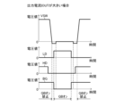
- FIG. 2 is a timing chart showing voltages at various parts of the half-bridge DC/DC converter shown in FIG. 1 when the output current is large.
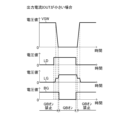
- FIG. 3 is a timing chart showing voltages at various parts of the half-bridge DC/DC converter shown in FIG. 1 when the output current is small.
- FIG. 4 is a diagram showing an example of the configuration of a level shifter.
- FIG. 5 is a diagram illustrating an embodiment of a half-bridge DC/DC converter.
- FIG. 6 is a timing chart showing voltages at various parts of the half-bridge DC/DC converter shown in FIG. 5 when the output current is large.
- FIG. 7 is a timing chart showing voltages at various parts of the half-bridge DC/DC converter shown in FIG. 5 when the output current is small.
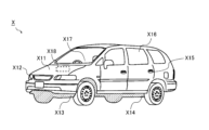
- FIG. 8 is an external view of the vehicle.
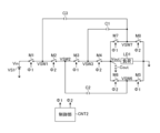
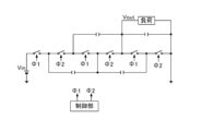
- FIG. 9 is a diagram showing the configuration of a Dixon type switched capacitor converter.
- FIG. 10 is a timing chart showing voltages at various parts of the switched capacitor converter shown in FIG.
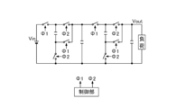
- FIG. 11 is a diagram showing a first example of a switched capacitor converter having a topology different from the Dixon type.
- FIG. 12 is a diagram showing a second example of a switched capacitor converter having a topology different from the Dixon type.
- FIG. 13 is a diagram showing a third example of a switched capacitor converter having a topology different from the Dixon type.
- FIG. 14 is a diagram showing a fourth example of a switched capacitor converter having a topology different from the Dixon type.
- a MOS field effect transistor is defined as having a gate structure that is a "layer made of a conductor or a semiconductor such as polysilicon with a low resistance value," “an insulating layer,” and "P-type, A field effect transistor consisting of at least three layers of "N-type or intrinsic semiconductor layers”. That is, the structure of the gate of the MOS field effect transistor is not limited to the three-layer structure of metal, oxide, and semiconductor.
- constant voltage means a voltage that is constant in an ideal state, and is actually a voltage that may vary slightly due to temperature changes and the like.
- the half-bridge DC/DC converter 100 of this comparative example includes a control unit CNT1, a level shifter LS1, drivers D1 and D2, N-channel MOS field effect transistors Q1 and Q2, an inductor L1, an output capacitor C0, and a boot. It has a strap circuit 10.
- N-channel MOS field effect transistors Q1 and Q2 are connected in series.
- the N-channel MOS field effect transistor Q1 is a high-side switch provided on the higher potential side than the N-channel MOS field effect transistor Q2.
- the N-channel MOS field effect transistor Q2 is a low-side switch provided on the lower potential side than the N-channel MOS field effect transistor Q1.
- the control unit CNT1 outputs control signals HD0 and LD. Basically, when one of the control signals HD0 and LD is at a HIGH level, the other is at a LOW level. Note that the control unit CNT1 provides a dead time in which both the control signals HD0 and LD are at LOW level.
- the level shifter LS1 outputs a control signal HD that is level-shifted from the control signal HD0.
- the driver D1 supplies a control signal HG obtained by amplifying the control signal HD to the gate of the N-channel MOS field effect transistor Q1.
- Driver D1 is driven with a voltage between bootstrap voltage BST and switching voltage VSW.
- the driver D2 supplies a control signal LG obtained by amplifying the control signal LD to the gate of the N-channel MOS field effect transistor Q2.
- the driver D2 is driven with a voltage between constant voltage VREG ( ⁇ input voltage VIN) and ground voltage.
- the input voltage VIN is applied to the drain of the N-channel MOS field effect transistor Q1.
- the source of the N-channel MOS field effect transistor Q2 is connected to ground potential.
- a switching voltage VSW is generated at the connection node between the N-channel MOS field effect transistors Q1 and Q2.
- the inductor L1 and the output capacitor C0 smooth the switching voltage VSW to generate the output voltage VOUT.
- the bootstrap circuit 10 generates a bootstrap voltage BST higher than the input voltage VIN.
- the bootstrap circuit 10 includes an AND gate A1, a level shifter LS2, a driver D3, a P-channel MOS field effect transistor QB, and a capacitor CB.
- the constant voltage VREG is applied to the source of the P-channel MOS field effect transistor QB.
- the drain of P-channel type MOS field effect transistor QB is connected to the first end of capacitor CB.
- a switching voltage VSW is applied to the second end of the capacitor CB.
- the bootstrap circuit 10 has a configuration in which the AND gate A1 generates a logical product of the control signal LD and the control signal LG, and the P-channel MOS field effect transistor QB is controlled based on the logical product.
- the level shifter LS2 level-shifts the output of the AND gate A1 and outputs it.
- the driver D3 supplies a control signal BG, which is an amplified and inverted output of the level shifter LS2, to the gate of the P-channel MOS field effect transistor QB.
- Driver D3 is driven with a voltage between bootstrap voltage BST and switching voltage VSW. Thereby, the N-channel MOS field effect transistor Q2 can be turned off after the P-channel MOS field effect transistor QB is turned off.
- the P-channel MOS field effect transistor QB can be turned off when the switching voltage VSW is greater than 0V.
- the AND of the control signal LD and the control signal LG is required, timing control becomes complicated.
- FIG. 4 is a diagram showing an example of the configuration of the level shifter LS2.
- the level shifter LS2 in the configuration example shown in FIG. L12, a third voltage line L13, and a fourth voltage line L14.
- the N-channel MOS field effect transistors 15 and 16 need to be elements having a breakdown voltage of the value of Vin. That is, since a plurality of elements having a breakdown voltage of the value Vin are required, the area of the level shifter LS2 of the configuration example shown in FIG. 4 becomes large.
- FIG. 5 is a diagram illustrating an embodiment of a half-bridge DC/DC converter.
- the half-bridge DC/DC converter 200 of this embodiment differs from the above-mentioned half-bridge DC/DC converter 100 in that it has a bootstrap circuit 20 instead of the bootstrap circuit 10, and is different from the above-mentioned half-bridge DC/DC converter 200 in that it has a bootstrap circuit 20 instead of the bootstrap circuit 10.
- /DC converter 100 is basically the same.
- FIG. 6 is a timing chart showing voltages at various parts of the half-bridge DC/DC converter 200 when the output current Iout is large.
- FIG. 7 is a timing chart showing voltages at various parts of the half-bridge DC/DC converter 200 when the output current Iout is small.
- the bootstrap circuit 20 includes a level shifter 30, a driver D3, a P-channel MOS field effect transistor QB, and a capacitor CB.
- the constant voltage VREG is applied to the source of the P-channel MOS field effect transistor QB.
- the drain of P-channel type MOS field effect transistor QB is connected to the first end of capacitor CB.
- a switching voltage VSW is applied to the second end of the capacitor CB.
- a control section composed of the level shifter 30 and the driver D3 controls the P-channel MOS field effect transistor QB based on the switching voltage VSW and the control signal LD.
- the level shifter 30 includes a resistor 31, a P-channel MOS field effect transistor 32, a resistor 33, and an N-channel MOS field effect transistor 34.
- the control signal LD is applied to the first end of the resistor 31.
- a second end of the resistor 31 is connected to the source of a P-channel MOS field effect transistor 32.
- the drain of the P-channel MOS field-effect transistor 32 is connected to the first end of the resistor 33, the drain of the N-channel MOS field-effect transistor 34, and the input terminal of the driver D3.
- the switching voltage VSW is applied to the gate of the P-channel MOS field effect transistor 32, the second end of the resistor 33, and the source of the N-channel MOS field effect transistor 34.
- the control signal HD is supplied to the gate of the N-channel MOS field effect transistor 34.
- the driver D3 amplifies and inverts the output of the level shifter 30 and supplies the control signal BG to the gate of the P-channel MOS field effect transistor QB.
- Driver D3 is driven with a voltage between bootstrap voltage BST and switching voltage VSW.
- the bootstrap circuit 20 controls the P-channel MOS field effect transistor QB based on the switching voltage VSW, timing control becomes easy. Specifically, the bootstrap circuit 20 controls the P-channel MOS field effect transistor QB based on the AND of the control signal LD and the inverted signal of the switching voltage VSW.
- the bootstrap circuit 20 uses a P-channel MOS field effect transistor QB, which is a switch, instead of a diode, the on-resistance of the N-channel MOS field effect transistor Q1 driven by the bootstrap voltage BST is further reduced. be able to.
- the resistor 33 can pull down the output of the level shifter 30 when the P-channel MOS field effect transistor 32 is off.
- N-channel MOS field effect transistor 34 is controlled by control signal HD.
- the N-channel MOS field effect transistor 34 can pull down the output of the level shifter 30 when the P-channel MOS field effect transistor 32 is off and the control signal HD is at a HIGH level. Since the bootstrap circuit 20 has a configuration including an N-channel MOS field effect transistor 34, it is possible to pull down the output of the level shifter 30 more reliably.
- the bootstrap circuit 20 can turn on the N-channel MOS field-effect transistor Q1 at an appropriate timing when the N-channel MOS field-effect transistors Q1 and Q2 are Si devices.
- the switching voltage VSW during dead time is several volts lower than when N-channel MOS field effect transistors Q1 and Q2 are Si devices.
- the control signal LG may be applied to the first end of the resistor 31 instead of the control signal LD.
- the P-channel MOS field effect transistor 32 is the only element that has a breakdown voltage of the value of Vin. Therefore, the level shifter 30 can have a smaller area than the level shifter LS2 in the configuration example shown in FIG.
- FIG. 8 is an external view of vehicle X.
- the vehicle X of this configuration example is equipped with various electronic devices X11 to X18 that operate by receiving voltage output from a battery (not shown). Note that the mounting positions of the electronic devices X11 to X18 in this figure may differ from the actual positions for convenience of illustration.
- the electronic device X11 is an engine control unit that performs engine-related controls (injection control, electronic throttle control, idling control, oxygen sensor heater control, auto cruise control, etc.).
- the electronic device X12 is a lamp control unit that performs lighting/extinguishing control for HID [high intensity discharged lamp], DRL [daytime running lamp], and the like.
- the electronic device X13 is a transmission control unit that performs control related to the transmission.
- the electronic device X14 is a braking unit that performs control related to the movement of the vehicle X (ABS [anti-lock brake system] control, EPS [electric power steering] control, electronic suspension control, etc.).
- ABS anti-lock brake system
- EPS electric power steering
- electronic suspension control etc.
- the electronic device X15 is a security control unit that controls the drive of door locks, security alarms, etc.
- Electronic equipment X16 is electronic equipment that is installed in vehicle It is.
- the electronic device X17 is an electronic device that is optionally installed in the vehicle X as a user option, such as an in-vehicle A/V [audio/visual] device, a car navigation system, and an ETC [electronic toll collection system].
- the electronic device X18 is an electronic device equipped with a high-voltage motor, such as an on-vehicle blower, an oil pump, a water pump, and a battery cooling fan.
- a high-voltage motor such as an on-vehicle blower, an oil pump, a water pump, and a battery cooling fan.
- half-bridge DC/DC converter 200 described above can be incorporated into any of the electronic devices X11 to X18. Further, the application of the half-bridge DC/DC converter 200 described above is not limited to a power source mounted on the vehicle X, but may be used as a power source mounted on, for example, industrial equipment.
- the bootstrap circuit 20 can also be installed in a power supply device other than the half-bridge DC/DC converter 200.
- the bootstrap circuit 20 can be mounted on a Dixon-type switched capacitor converter shown in FIG.
- FIG. 10 is a timing chart showing voltages at various parts of the switched capacitor converter shown in FIG.
- the switched capacitor converter shown in FIG. 9 includes switching elements M1 to M8, capacitors C1 to C3, an output capacitor Cout, and a control unit CNT2.
- the first end of the switching element M1 is connected to the positive electrode of the DC voltage source VS1.
- the negative pole of DC voltage source VS1 is connected to ground potential.
- the DC voltage source VS1 supplies the input voltage Vin to the first end of the switching element M1.
- the second end of the switching element M1 is connected to the first end of the switching element M2 and the first end of the capacitor C3.
- a second end of switching element M2 is connected to a first end of switching element M3 and a first end of capacitor C2.
- a second end of switching element M3 is connected to a first end of switching element M4 and a first end of capacitor C1.
- the second end of the switching element M4 is connected to the first end of the switching element M7, the first end of the load LD1, the first end of the switching element M6, and the first end of the output capacitor Cout.
- a second end of switching element M7 is connected to a first end of switching element M8, a second end of capacitor C1, and a second end of capacitor C3.
- a second end of switching element M6 is connected to a first end of switching element M5 and a second end of capacitor C2.
- the second end of the switching element M8, the second end of the load LD1, the second end of the switching element M5, and the second end of the output capacitor Cout are connected to the ground potential.
- the control unit CNT2 controls the switching elements M1, M3, M5, and M7 using the first control signal ⁇ 1, and controls the switching elements M2, M4, M6, and M8 using the second control signal ⁇ 2.
- the control unit CNT2 performs complementary on/off control of the switching elements M1, M3, M5, and M7 and the switching elements M2, M4, M6, and M8.
- the switching voltage VSW1 switches between the value of Vin and the value of Vin ⁇ 3/4.
- Switching voltage VSW1 is generated at the connection node between switching element M1 and switching element M2.
- the switching voltage VSW2 switches between a value of Vin ⁇ 3/4 and a value of Vin/2.
- Switching voltage VSW2 is generated at the connection node between switching element M2 and switching element M3.
- the switching voltage VSW3 switches between a value of Vin/2 and a value of Vin/4.
- Switching voltage VSW3 is generated at the connection node between switching element M3 and switching element M4.
- the switching voltage VSW6 switches between the value of Vin/4 and 0 (ground potential). Switching voltage VSW6 is generated at the connection node between switching element M5 and switching element M6.
- the switching voltage VSW7 switches between the value of Vin/4 and 0 (ground potential). Switching voltage VSW7 is generated at the connection node between switching element M7 and switching element M8.
- the output voltage Vout has a value of Vin/4.
- the output voltage Vout is generated at the connection node between the switching element M4, the switching element M6, and the switching element M7.
- the output voltage Vout is supplied to the load LD1.
- the switching elements M1 to M8 are N-channel MOS field effect transistors
- six bootstrap circuits 20 for driving each of the switching elements M1 to M4, M6, and M7 are implemented in the switched capacitor converter shown in FIG. It's fine if it's installed.
- the arrangement of the DC voltage source VS1 and the load LD1 may be exchanged.
- the voltage supplied from the switched capacitor converter shown in FIG. 9 to the load LD1 (the output voltage of the switched capacitor converter shown in FIG. 9) is the same as that of the DC voltage source VS1. is larger than the voltage supplied to the switched capacitor converter shown in FIG. 9 (input voltage of the switched capacitor converter shown in FIG. 9).
- the bootstrap circuit 20 can also be installed in a switched capacitor converter, which has a topology different from the Dixon type.
- switched capacitor converters having a topology different from the Dickson type include switched capacitor converters shown in FIGS. 11 to 14.
- the bootstrap circuit (20) described above includes a first switch (QB) configured to apply a constant voltage to the first end, and a second end of the first switch connected to the first end, a capacitor (CB) configured to have a switching voltage applied to its second terminal; and a control unit (30, D3) configured to control the first switch based on the switching voltage and the first control signal.
- the switching voltage is a voltage generated at a connection node between a first switching element (Q1) and a second switching element (Q2)
- the second switching element is a voltage generated at a connection node between the first switching element (Q1) and the second switching element (Q2).
- This configuration (first configuration) is a switching element provided on the lower potential side and configured to perform switching based on the first control signal.
- the bootstrap circuit with the first configuration can further reduce the on-resistance of the switching element (first switching element) driven by the bootstrap voltage, and facilitate timing control.
- control section may have a configuration (second configuration) including a level shifter (30) configured to level shift the first control signal.
- the bootstrap circuit of the second configuration can use a level shifter with a small circuit area.
- the level shifter includes an N-channel MOS field effect transistor (32), and the N-channel MOS field effect transistor has a gate supplied with the switching voltage. (a third configuration).
- the high voltage elements can be only N-channel MOS field effect transistors.
- the N-channel MOS field effect transistor may have a configuration in which the first control signal is supplied to the drain (fourth configuration).
- the high voltage elements can be only N-channel MOS field effect transistors.
- the level shifter has a resistor (33) provided between the source and drain of the N-channel MOS field effect transistor (fifth configuration); Good too.
- the bootstrap circuit with the fifth configuration can pull down the output of the level shifter when the N-channel MOS field effect transistor is off.
- the first switching element is a switching element configured to switch based on a second control signal
- the level shifter is a switching element configured to perform switching based on a second control signal
- the level shifter is a switching element configured to perform switching based on a second control signal.
- a second switch (34) may be provided between the source and drain of the transistor, and the second switch may be configured to perform switching based on the second control signal (sixth configuration). good.
- the bootstrap circuit with the sixth configuration can pull down the output of the level shifter when the N-channel MOS field effect transistor is off.
- each of the first switching element and the second switching element is a Si device, and the first control signal is configured to drive the second switching element.
- the configuration (seventh configuration) may be an input signal of the configured driver.
- the bootstrap circuit with the seventh configuration can turn on the first switch at a timing suitable for the first switching element and the second switching element.
- each of the first switching element and the second switching element is a GAN device or a SiC device, and the first control signal drives the second switching element.
- the configuration may be an output signal of a driver configured to do so.
- the bootstrap circuit with the eighth configuration can turn on the first switch at a timing suitable for the first switching element and the second switching element.
- the first switch may be turned off when the switching voltage is greater than a predetermined value (ninth configuration).
- the bootstrap circuit with the ninth configuration can prevent the switching voltage from taking an abnormal value.
- the power supply device (200) described above has a configuration (tenth configuration) including a bootstrap circuit having any of the first to ninth configurations, the first switching element, and the second switching element. be.
- the power supply device with the tenth configuration can further reduce the on-resistance of the switching element (first switching element) driven by the bootstrap voltage, and facilitate timing control of the bootstrap circuit.
- the vehicle (X) described above has a configuration (eleventh configuration) that includes the power supply device of the tenth configuration.
- the on-resistance of the switching element (first switching element) driven by the bootstrap voltage can be further lowered, and timing control of the bootstrap circuit becomes easier.
- Bootstrap circuit 12 Inverter 13 to 16, 34, Q1, Q2 N-channel type MOS field effect transistor 17, 18, 32, QB P-channel type MOS field effect transistor 30, LS1, LS2 Level shifter 31, 33 Resistor 100, 200 Half-bridge DC/DC converter A1 AND gate C0, Cout Output capacitor C1-C3, CB Capacitor CNT1, CNT2 Control section D1-D3 Driver L1 Inductor L11-L14 1st-4th voltage line LD1 Load M1-M8 Switching element X Vehicle X11-X18 Electronic equipment
Landscapes
- Engineering & Computer Science (AREA)
- Power Engineering (AREA)
- Mechanical Engineering (AREA)
- Dc-Dc Converters (AREA)
- Power Conversion In General (AREA)
Priority Applications (2)
| Application Number | Priority Date | Filing Date | Title |
|---|---|---|---|
| JP2024520394A JPWO2023218988A1 (https=) | 2022-05-11 | 2023-04-27 | |
| US18/938,993 US20250062688A1 (en) | 2022-05-11 | 2024-11-06 | Bootstrap circuit, power supply device, and vehicle |
Applications Claiming Priority (2)
| Application Number | Priority Date | Filing Date | Title |
|---|---|---|---|
| JP2022078098 | 2022-05-11 | ||
| JP2022-078098 | 2022-05-11 |
Related Child Applications (1)
| Application Number | Title | Priority Date | Filing Date |
|---|---|---|---|
| US18/938,993 Continuation US20250062688A1 (en) | 2022-05-11 | 2024-11-06 | Bootstrap circuit, power supply device, and vehicle |
Publications (1)
| Publication Number | Publication Date |
|---|---|
| WO2023218988A1 true WO2023218988A1 (ja) | 2023-11-16 |
Family
ID=88730392
Family Applications (1)
| Application Number | Title | Priority Date | Filing Date |
|---|---|---|---|
| PCT/JP2023/016671 Ceased WO2023218988A1 (ja) | 2022-05-11 | 2023-04-27 | ブートストラップ回路、電源装置、及び車両 |
Country Status (3)
| Country | Link |
|---|---|
| US (1) | US20250062688A1 (https=) |
| JP (1) | JPWO2023218988A1 (https=) |
| WO (1) | WO2023218988A1 (https=) |
Citations (3)
| Publication number | Priority date | Publication date | Assignee | Title |
|---|---|---|---|---|
| JP2015511112A (ja) * | 2012-03-16 | 2015-04-13 | 日本テキサス・インスツルメンツ株式会社 | GaNFETのゲートの保護のためのドライバ回路のためのシステム及び装置 |
| WO2021117821A1 (ja) * | 2019-12-12 | 2021-06-17 | ローム株式会社 | スイッチング回路のゲート駆動回路およびスイッチング電源の制御回路 |
| JP2021150532A (ja) * | 2020-03-19 | 2021-09-27 | 株式会社東芝 | 半導体装置 |
-
2023
- 2023-04-27 JP JP2024520394A patent/JPWO2023218988A1/ja active Pending
- 2023-04-27 WO PCT/JP2023/016671 patent/WO2023218988A1/ja not_active Ceased
-
2024
- 2024-11-06 US US18/938,993 patent/US20250062688A1/en active Pending
Patent Citations (3)
| Publication number | Priority date | Publication date | Assignee | Title |
|---|---|---|---|---|
| JP2015511112A (ja) * | 2012-03-16 | 2015-04-13 | 日本テキサス・インスツルメンツ株式会社 | GaNFETのゲートの保護のためのドライバ回路のためのシステム及び装置 |
| WO2021117821A1 (ja) * | 2019-12-12 | 2021-06-17 | ローム株式会社 | スイッチング回路のゲート駆動回路およびスイッチング電源の制御回路 |
| JP2021150532A (ja) * | 2020-03-19 | 2021-09-27 | 株式会社東芝 | 半導体装置 |
Also Published As
| Publication number | Publication date |
|---|---|
| JPWO2023218988A1 (https=) | 2023-11-16 |
| US20250062688A1 (en) | 2025-02-20 |
Similar Documents
| Publication | Publication Date | Title |
|---|---|---|
| US11848611B2 (en) | Switching power supply device | |
| US9350238B2 (en) | Power supply device for vehicle including a boosting converter circuit | |
| US10256623B2 (en) | Power control device | |
| US20120154014A1 (en) | Level shift circuit and switching power supply device | |
| US10355589B2 (en) | Switching regulator | |
| JP7489244B2 (ja) | リニア電源回路 | |
| JP2020135372A (ja) | 電源回路 | |
| JP2020071710A (ja) | リニア電源回路 | |
| US11296686B2 (en) | Method for operating an electrical circuit, electrical circuit, and motor vehicle | |
| CN114041262B (zh) | 开关电源装置 | |
| JP2006314154A (ja) | 電力変換器 | |
| JP2000261301A (ja) | 電源供給装置及び電源供給方法 | |
| JP2020072399A (ja) | 差動増幅器 | |
| WO2023218988A1 (ja) | ブートストラップ回路、電源装置、及び車両 | |
| US12463645B2 (en) | Level shifter, drive circuit, switching power supply device, and vehicle | |
| CN115943548A (zh) | 开关电源装置、开关控制装置、车载设备和车辆 | |
| US12425020B2 (en) | Switch circuit, switched capacitor converter, and vehicle | |
| JP2013258549A (ja) | ドライバ回路 | |
| JP6968657B2 (ja) | 積分回路 | |
| WO2023181660A1 (ja) | 駆動装置、スイッチング電源装置、及び車両 | |
| US12494712B2 (en) | Control circuit, switched capacitor converter, and vehicle | |
| WO2022190855A1 (ja) | スイッチング電源装置、スイッチ制御装置、車載機器、及び車両 | |
| US11606033B2 (en) | Switching power supply device | |
| WO2024018815A1 (ja) | リニア電源回路及び車両 | |
| JP2025042438A (ja) | ゲート駆動回路、電源制御装置、電源装置、及び車両 |
Legal Events
| Date | Code | Title | Description |
|---|---|---|---|
| 121 | Ep: the epo has been informed by wipo that ep was designated in this application |
Ref document number: 23803467 Country of ref document: EP Kind code of ref document: A1 |
|
| WWE | Wipo information: entry into national phase |
Ref document number: 2024520394 Country of ref document: JP |
|
| NENP | Non-entry into the national phase |
Ref country code: DE |
|
| 122 | Ep: pct application non-entry in european phase |
Ref document number: 23803467 Country of ref document: EP Kind code of ref document: A1 |