WO2023214467A1 - 光給電システム及び異常箇所検出方法 - Google Patents
光給電システム及び異常箇所検出方法 Download PDFInfo
- Publication number
- WO2023214467A1 WO2023214467A1 PCT/JP2022/019588 JP2022019588W WO2023214467A1 WO 2023214467 A1 WO2023214467 A1 WO 2023214467A1 JP 2022019588 W JP2022019588 W JP 2022019588W WO 2023214467 A1 WO2023214467 A1 WO 2023214467A1
- Authority
- WO
- WIPO (PCT)
- Prior art keywords
- optical
- light
- power supply
- photoelectric conversion
- conversion element
- Prior art date
- Legal status (The legal status is an assumption and is not a legal conclusion. Google has not performed a legal analysis and makes no representation as to the accuracy of the status listed.)
- Ceased
Links
Images


Classifications
-
- H—ELECTRICITY
- H04—ELECTRIC COMMUNICATION TECHNIQUE
- H04B—TRANSMISSION
- H04B10/00—Transmission systems employing electromagnetic waves other than radio-waves, e.g. infrared, visible or ultraviolet light, or employing corpuscular radiation, e.g. quantum communication
- H04B10/07—Arrangements for monitoring or testing transmission systems; Arrangements for fault measurement of transmission systems
- H04B10/071—Arrangements for monitoring or testing transmission systems; Arrangements for fault measurement of transmission systems using a reflected signal, e.g. using optical time domain reflectometers [OTDR]
-
- H—ELECTRICITY
- H02—GENERATION; CONVERSION OR DISTRIBUTION OF ELECTRIC POWER
- H02J—ELECTRIC POWER NETWORKS; CIRCUIT ARRANGEMENTS OR SYSTEMS FOR SUPPLYING OR DISTRIBUTING ELECTRIC POWER; SYSTEMS FOR STORING ELECTRIC ENERGY
- H02J50/00—Circuit arrangements or systems for wireless supply or distribution of electric power
- H02J50/30—Circuit arrangements or systems for wireless supply or distribution of electric power using light, e.g. lasers
-
- H—ELECTRICITY
- H04—ELECTRIC COMMUNICATION TECHNIQUE
- H04B—TRANSMISSION
- H04B10/00—Transmission systems employing electromagnetic waves other than radio-waves, e.g. infrared, visible or ultraviolet light, or employing corpuscular radiation, e.g. quantum communication
- H04B10/25—Arrangements specific to fibre transmission
-
- H—ELECTRICITY
- H04—ELECTRIC COMMUNICATION TECHNIQUE
- H04B—TRANSMISSION
- H04B10/00—Transmission systems employing electromagnetic waves other than radio-waves, e.g. infrared, visible or ultraviolet light, or employing corpuscular radiation, e.g. quantum communication
- H04B10/80—Optical aspects relating to the use of optical transmission for specific applications, not provided for in groups H04B10/03 - H04B10/70, e.g. optical power feeding or optical transmission through water
-
- H—ELECTRICITY
- H04—ELECTRIC COMMUNICATION TECHNIQUE
- H04B—TRANSMISSION
- H04B10/00—Transmission systems employing electromagnetic waves other than radio-waves, e.g. infrared, visible or ultraviolet light, or employing corpuscular radiation, e.g. quantum communication
- H04B10/80—Optical aspects relating to the use of optical transmission for specific applications, not provided for in groups H04B10/03 - H04B10/70, e.g. optical power feeding or optical transmission through water
- H04B10/806—Arrangements for feeding power
- H04B10/807—Optical power feeding, i.e. transmitting power using an optical signal
Definitions
- the present disclosure relates to an optical power supply system that supplies power to a plurality of optical nodes by connecting the optical nodes in series to an optical fiber.
- Optical fiber networks especially access networks that connect communication equipment installed in communication buildings and communication terminals on the user side, need to be connected to new routes or changed routes in order to use equipment efficiently during installation and maintenance.
- Optical line switching is performed at a certain frequency. Normally, such work involves going to the site and manually switching the optical fiber connections, but a technology has been proposed that allows the switching of the optical fiber connections to be performed remotely.
- Non-Patent Documents 1 and 2 in a system consisting of a power supply control light source installed in a power supply environment such as a laboratory, and one or more optical nodes located remotely, multiple optical nodes are connected in series to an optical fiber.
- a method has been proposed in which the functions of optical power supply and control of multiple optical switches included in an optical node can be simultaneously realized using a single light source by connecting the optical nodes.
- This optical node is installed within an optical fiber network, and performs mutual connection and switching on an optical fiber basis.
- an optical fiber network made up of optical nodes, if any abnormality such as a failure occurs in either the optical fibers connecting the optical nodes or the optical nodes, it is necessary to detect the abnormality and restore it.
- an optical fiber network composed of optical nodes there is currently no method or system for detecting abnormalities.
- optical nodes have a structure that is driven by optically fed light, they are required to operate with low power consumption, so they do not require new sensors to detect abnormalities, and only the functions they currently have are used to detect abnormalities. A method and system for detecting this is desirable.
- the present disclosure aims to enable abnormal locations to be detected from a distance in an optical power supply system that supplies power to a plurality of optical nodes by connecting the optical nodes in series to an optical fiber.
- the optical power supply system of the present disclosure is an optical power supply system that supplies power to a plurality of optical nodes by connecting the optical nodes in series to an optical fiber, and includes the communication device and the optical node of the present disclosure.
- the communication device of the present disclosure includes: a light source that outputs power supply light to a plurality of optical nodes connected in series to an optical fiber; an optical tester that transmits test light from the light source side of the optical fiber toward the plurality of optical nodes and detects reflected light of the test light; Equipped with Determining the point where optical loss occurs using the test waveform obtained with the optical tester, The abnormal location is determined based on the location where the optical loss occurs.
- the optical node device of the present disclosure includes: a photoelectric conversion element that converts feeding light propagated through an optical fiber into electricity; a power storage unit that stores power converted by the photoelectric conversion element; an optical switch that switches the output destination of the power supply light between a photoelectric conversion element provided in the optical node and another optical node connected to the optical fiber; a test light cut filter that reflects test light output from the optical switch to the photoelectric conversion element; The connection of the optical switch is changed according to a control signal superimposed on the power supply light, and the stored voltage value of the power storage unit is checked at a certain time interval, and the stored voltage value of the power storage unit is determined to be below a certain value.
- a control unit that automatically switches the optical switch to the photoelectric conversion element provided in the self-optical node; Equipped with
- the abnormal location detection method of the present disclosure is a method executed by the optical power supply system of the present disclosure, comprising:
- the plurality of optical nodes are an optical switch that switches the output destination of the feeding light propagated through the optical fiber between a photoelectric conversion element provided in the optical node and another optical node connected to the optical fiber; a test light cut filter that reflects the test light output from the optical switch to the photoelectric conversion element toward the optical tester; Equipped with The control unit provided in any of the plurality of optical nodes switches the connection of the optical switch according to a control signal superimposed on the power supply light, The test light is reflected by the test light cut filter.
- the control unit checks the stored voltage value of the power storage unit at fixed time intervals, and when the stored voltage value of the power storage unit becomes equal to or lower than a certain voltage value, the control unit activates the optical switch.
- the photoelectric conversion element may be automatically switched to the photoelectric conversion element provided in the self-optical node.
- a test waveform obtained by the optical tester is used to determine the point where optical loss occurs, and a distance of the optical fiber from the optical tester to each of the plurality of optical nodes is determined.
- a distance of the optical fiber from the optical tester to each of the plurality of optical nodes is determined.
- the test light is transmitted from the optical tester. You may. In this case, if no optical loss occurs in the test waveform obtained by the optical tester, for each of the plurality of optical nodes, sequentially connect the optical switch to the self-optical node starting from the side closest to the light source. You may make it switch to the said photoelectric conversion element provided.
- an abnormal location can be detected from a distance in an optical power supply system that supplies power to a plurality of optical nodes by connecting the optical nodes in series to an optical fiber.
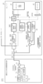
- FIG. 1 is an example of a system configuration of an optical power feeding system according to the present disclosure.
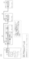
- 1 is an example of a system configuration of an optical power feeding system according to the present disclosure.
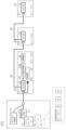
- 1 is an example of a system configuration of an optical power feeding system according to the present disclosure.
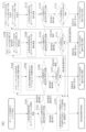
- FIG. 2 is a flow diagram illustrating an example of an abnormal location detection method according to the present disclosure.
- FIG. 1 shows an example of the basic configuration of an optical power feeding system.
- the optical power supply system of the present disclosure includes a power supply control light source 11 that outputs power supply light to a power supply/control optical fiber 30, and a plurality of optical nodes 20 connected in series to the power supply/control optical fiber 30.
- a power supply control light source 11 that outputs power supply light to a power supply/control optical fiber 30, and a plurality of optical nodes 20 connected in series to the power supply/control optical fiber 30.
- a power supply control light source 11 that outputs power supply light to a power supply/control optical fiber 30, and a plurality of optical nodes 20 connected in series to the power supply/control optical fiber 30.
- the number of optical nodes 20 connected in series may be any number greater than or equal to two.
- Each optical node 20 is an optical coupler 21 that branches the power supply light into two; a photoelectric conversion element 23B that converts power supply light into electricity; a power storage unit 26 that stores power converted by the photoelectric conversion element 23B; Switching the output destination of the power feeding light propagated through the power feeding/controlling optical fiber 30 between the photoelectric conversion element 23B provided in the own optical node 20 and another optical node 20 connected to the power feeding/controlling optical fiber 30 1 ⁇ 2 optical switch 22, a photoelectric conversion element 23C that receives a control signal superimposed on the power supply light; A control unit 25 that switches the connection of the 1 ⁇ 2 optical switch 22 according to the control signal received by the photoelectric conversion element 23C; Equipped with Hereinafter, when the photoelectric conversion elements 23B and 23C are not distinguished, they will be referred to as photoelectric conversion elements 23.
- Each optical node 20 is equipped with a 1 ⁇ 2 optical switch 22, which switches whether the transmitted optical power feeding light is taken into the photoelectric conversion element 23 of each optical node 20 or sent to the rear optical node 20.
- This 1 ⁇ 2 optical switch 22 is switched by a control signal superimposed on the optical power supply light. In this way, the 1 ⁇ 2 optical switch 22 is switched so that the power feeding control light source 11 and each optical node 20 can simultaneously communicate one-on-one using control signals.
- FIG. 2 A more detailed configuration of the optical power supply system is shown in Figure 2.
- Optical power supply light from a power supply control light source 11 in a communication building is superimposed with a control signal in an optical modulator 12 and transmitted to an optical node 20 .
- the upstream control signal from the optical node 20 is output from the circulator 13 to the optical receiver 14 and received by the optical receiver 14 .
- the controller PC 15 outputs a control signal to the optical modulator 12, and the optical modulator 12 superimposes the control signal on the feeding light.
- the optical receiver 14 outputs the received signal to the controller PC 15. Thereby, the controller PC 15 transmits and receives control signals to and from each optical node 20.
- the control unit 25 of the optical node 20 receives the control signal superimposed on the optical power supply light, and controls the 1 ⁇ 2 optical switch 22 and other devices 41 and 42. Further, the optical node 20 converts the optical power supply light into electricity using the photoelectric conversion element 23B, and stores the electricity in the device power storage unit 26D and the control unit power storage unit 26C. The controller 25 of the optical node 20 and the devices 41 and 42 are driven by this stored power.
- the device power storage unit 26D and the control unit power storage unit 26C are not distinguished, they are referred to as power storage unit 26.
- the control unit 25 and the devices 41 and 42 cannot be controlled or driven when the voltage falls below a driveable voltage value.
- each of the optical nodes 20 can perform optical power feeding by sequentially switching each 1 ⁇ 2 optical switch 22. Therefore, in the optical power supply system of the present disclosure, a certain amount of power is always stored in the power storage unit 26 provided in each optical node 20, and the control unit 25 provided in each optical node 20 is maintained in a driveable state. This is a prerequisite for operation.
- the optical power supply system of the present disclosure uses a control signal from the power supply control light source 11 to control the optical node 20 so that the power storage unit 26 of each optical node 20 always stores a constant amount of power.
- the amount of power stored in the power storage unit 26 is inquired and confirmed at any time.
- the optical power feeding system of the present disclosure includes the optical power feeding system shown in FIGS. 1 and 2, and further includes an optical tester (light pulse tester 17 shown in FIG. 4) and a test light cut filter (reference numeral 28 shown in FIGS. 4 and 5). ).
- an optical pulse tester (numeral 17 shown in FIG. 4) is used as an example of an optical tester.
- the optical pulse tester (numeral 17 shown in FIG. 4) transmits test light from the power supply control light source 11 side of the power supply/control optical fiber 30 toward the plurality of optical nodes 20, and detects reflected light of the test light.
- the test light cut filter (numeral 28 shown in FIGS. 4 and 5) reflects the test light output from the 1 ⁇ 2 optical switch 22 to the photoelectric conversion element 23B toward the pulsed light tester 17.
- the optical power feeding system of the present disclosure executes the abnormal location detection method of the present disclosure.
- the control unit 25 switches the connection of the 1 ⁇ 2 optical switch 22 according to the control signal superimposed on the power supply light, and causes the test light to be reflected on the test light cut filter 28.
- the optical power feeding system of the present disclosure includes an optical pulse tester (numeral 17 shown in FIG. 4) and a test light cut filter (numeral 28 shown in FIGS. 4 and 5), and is capable of performing the abnormal location detection method of the present disclosure.
- an optical pulse tester numbereral 17 shown in FIG. 4
- a test light cut filter numbereral 28 shown in FIGS. 4 and 5
- the optical fiber network configured by the optical nodes 20
- if an abnormality occurs in any section of the power supply/control optical fiber or device of the serial type optical nodes 20 the current equipment as shown in FIGS. This makes it possible to isolate failures remotely using only the functions that are provided.
- each optical node 20 drives the control unit 25 and the devices 41 and 42 within the optical node 20 using the electric power stored in the power storage unit 26.
- the power stored in the power storage unit 26 is It decreases over time due to natural discharge, etc.
- the control unit 25 checks the stored voltage value of the power storage unit 26 at regular time intervals, and The feature is that when the value is below the value, the control unit 25 can automatically switch the 1 ⁇ 2 optical switch 22 to a direction in which the self-optical node 20 can receive light.
- any optical node 20 continues to be unable to receive optically supplied light, the voltage value of the power storage unit 26 of any optical node 20 further drops, and the control unit 25 becomes unable to drive due to the voltage drop. Even if the 1 ⁇ 2 optical switch 22 becomes unable to be driven, the 1 ⁇ 2 optical switch 22 of the corresponding optical node 20 is switched to the direction in which the optical node 20 can receive light.
- a server 16 is installed that cooperates with a controller PC 15 that operates the power supply control light source 11.
- This server 16 is characterized in that it cooperates with the controller PC 15 and holds information regarding the connection order of the plurality of optical nodes 20 from the power supply control light source 11 through a single optical fiber.
- the optical nodes 20 are given unique identifiers, and the order in which they are connected is maintained by the server 16.
- the optical node 20#1 is the identifier, and the optical node 20 connects to the power supply/control optical fiber 30 in the order of optical node 20#1, optical node 20#2, and optical node 20#3.
- This server 16 stores information that it is connected.
- a third embodiment of the optical power supply system of the present disclosure will be described in detail.
- a specific test wavelength is applied to the power supply/control optical fiber 30 using an optical pulse tester 17 from the upper side of the optical node 20#1, such as inside a communication building.
- the configuration is such that a pulsed test light can be inserted.
- the optical node 20 is also equipped with a test light cut filter 28 such as an FBG (fiber grating) that blocks light of this test wavelength by reflecting it.
- FBG fiber grating
- FIG. 5 A more detailed configuration of the optical power supply system is shown in FIG. As shown in FIG. 5, a test light cut filter 28 is inserted between the 1 ⁇ 2 optical switch 22 and the photoelectric conversion element 23B in the optical node 20. With this configuration, the pulsed test light reaches the 1 ⁇ 2 optical switch 22. Furthermore, when the inserted pulse test light reaches the test light cut filter 28, a reflection point is confirmed at the position of the test light cut filter 28 in the pulse test waveform, so it is possible to confirm that the pulse test light has arrived. Become.
- the server 16 that cooperates with the controller PC 15 that operates the power supply control light source 11 is connected to the power supply control light source 11 and the nearest optical node 20#1, and the optical fiber length (line length) between the power supply control light source 11 and the nearest optical node 20#1. ) data.
- a light pulse test is carried out using the light pulse tester 17. If a location where optical loss occurs is confirmed in the test waveform, the server 16 measures the distance between the power supply control light source 11 and the location where optical loss occurs. Compare the distance to the point where the loss occurred measured with the optical pulse tester 17, the connection order of the optical nodes 20 managed by the server 16, and the line length of the corresponding power supply/control optical fiber 30 to determine the optical loss.
- a feature is that it is possible to determine which optical node 20 or which optical fiber section between optical nodes 20 the occurrence point is located on.
- the server 16 implements the separation flow shown in FIG.
- the server 16 can also be realized by a computer and a program, and the program can be recorded on a recording medium or provided through a network.
- a configuration in which the controller PC 15 has the functions of the server 16 by executing the program on the controller PC 15 can also be adopted.
- three optical nodes 20 are connected.
- an optical pulse test is performed using the optical pulse tester 17 (S101), and the presence or absence of an optical loss occurrence location is confirmed using the test waveform obtained in the optical pulse test (S102). If a light loss location is confirmed, it is compared with data stored in the server 16 (S103) to detect an abnormal location. If there is no location where optical loss occurs, confirmation is performed in order starting from the optical node 20#1 that is closer to the power supply control light source 11.
- the optical node 20#1 is instructed to switch the 1 ⁇ 2 optical switch 22 to the light input side of the optical node 20#1 using a control signal (S104). Even if the power storage unit 26 of the optical node 20#1 does not have enough stored power to respond at this point, if the optical node 20#1 is operating normally, the characteristics shown in the first embodiment Therefore, the 1 ⁇ 2 optical switch 22 should have been automatically switched to the direction in which the own optical node 20 can receive light.
- a light pulse test is performed (S105), and the presence or absence of a location where light loss occurs is confirmed using the test waveform obtained in the light pulse test (S106). If an optical loss location is confirmed (there is a loss occurrence location in S106), it is compared with data stored in the server 16 (S103) to detect an abnormal location. If no optical loss location is confirmed (no loss occurrence location in S106), the reflection point of the optical node 20#1 is confirmed using the test waveform (S107).
- the 1 ⁇ 2 optical switch 22 is normally switched to the direction in which the self-optical node 20 can receive light, the reflection of the test light cut filter 28 installed behind the 1 ⁇ 2 optical switch 22 will be reflected from the far side of the test waveform. It should be visible at the edge (there is a reflection point in S107). If the reflection point cannot be confirmed (no reflection point in S107), it means that the 1 ⁇ 2 optical switch 22 has not been switched to the direction in which the self-light node 20 can receive light. Therefore, it is determined that there is a possibility that some abnormality has occurred in the optical node 20#1. If the reflection point can be confirmed, the 1 ⁇ 2 optical switch 22 of the optical node 20#1 is determined to be normal, and the next step is to confirm the optical node 20#2.
- the event that triggers the start of the separation flow is the occurrence of trouble in the control system of the optical node 20, and the control of inquiries and responses regarding the amount of electricity stored between the power supply control light source 11 and each optical node 20. It is characterized in that the separation flow is started irregularly in response to the occurrence of an event such as no response from the optical node 20 during communication exchange.
Landscapes
- Engineering & Computer Science (AREA)
- Physics & Mathematics (AREA)
- Computer Networks & Wireless Communication (AREA)
- Electromagnetism (AREA)
- Signal Processing (AREA)
- Optics & Photonics (AREA)
- Power Engineering (AREA)
- Optical Communication System (AREA)
Abstract
Description
光ファイバに直列に接続されている複数の光ノードに給電光を出力する光源と、
前記光ファイバの前記光源側から前記複数の光ノードに向けて試験光を送信し、前記試験光の反射光を検出する光試験器と、
を備え、
前記光試験器で得られた試験波形を用いて光損失の発生地点を判定し、
光損失の発生地点に基づいて、異常箇所を判定する。
光ファイバで伝搬された給電光を電気に変換する光電変換素子と、
前記光電変換素子で変換された電力を蓄電する蓄電部と、
前記給電光の出力先を、自光ノードに備わる光電変換素子と前記光ファイバに接続されている他の光ノードとで切り替える光スイッチと、
前記光スイッチから前記光電変換素子に出力される試験光を反射する試験光カットフィルタと、
前記給電光に重畳されている制御信号に従って前記光スイッチの接続を切り替え、かつ一定時間間隔で前記蓄電部の蓄電電圧値の確認を行い、前記蓄電部の蓄電電圧値が一定値以下になった場合、前記光スイッチを自光ノードに備わる前記光電変換素子に自動的に切り替える制御部と、
を備える。
前記複数の光ノードが、
前記光ファイバで伝搬される前記給電光の出力先を、自光ノードに備わる光電変換素子と前記光ファイバに接続されている他の光ノードとで切り替える光スイッチと、
前記光スイッチから前記光電変換素子に出力される前記試験光を、前記光試験器に向けて反射する試験光カットフィルタと、
を備え、
前記複数の光ノードのいずれかに備わる前記制御部が、前記給電光に重畳されている制御信号に従って、前記光スイッチの接続を切り替え、
前記試験光を前記試験光カットフィルタに反射させる。
(i)前記複数の光ノードのいずれかに異常が発生している場合はどの光ノードに異常が発生しているか、
(ii)前記複数の光ノードの光ノード間のいずれかの区間に異常が発生している場合はどの区間の光ファイバに異常が発生しているか、
の判定を行ってもよい。
前記光電変換素子に切り替えた光ノードにおける前記試験光の反射がない場合、当該光ノードにおいて異常が発生していると判定してもよい。
この場合、前記光試験器で得られた試験波形において、光損失が発生していない場合、前記複数の光ノードのそれぞれに対し、前記光源に近い側から順次、前記光スイッチを自光ノードに備わる前記光電変換素子に切り替えさせてもよい。
図1に、光給電システムの基本構成例を示す。本開示の光給電システムは、給電・制御用光ファイバ30に給電光を出力する給電制御光源11と、給電・制御用光ファイバ30に直列に接続されている複数の光ノード20と、を備える。本実施形態では、理解が容易になるよう、3台の光ノード20のみが接続される例を示すが、直列に接続される光ノード20の数は2以上の任意の数でありうる。
給電光を2分岐する光カプラ21と、
給電光を電気に変換する光電変換素子23Bと、
光電変換素子23Bで変換された電力を蓄電する蓄電部26と、
給電・制御用光ファイバ30で伝搬される給電光の出力先を、自光ノード20に備わる光電変換素子23Bと給電・制御用光ファイバ30に接続されている他の光ノード20とで切り替える1×2光スイッチ22と、
給電光に重畳されている制御信号を受信する光電変換素子23Cと、
光電変換素子23Cの受信した制御信号に従って1×2光スイッチ22の接続を切り替える制御部25と、
を備える。
以下、光電変換素子23B及び23Cを区別しない場合は光電変換素子23と表記する。
本開示の光給電システムの第1の実施形態を詳細に説明する。既に述べたように、各光ノード20は、蓄電部26に蓄えられた電力により、制御部25、光ノード20内のデバイス41及び42の駆動を行う。各光ノード20は、自光ノード20が光給電光を受光していない時、即ち1×2光スイッチ22を後方の光ノード20側に切替えている場合、蓄電部26に蓄えられた電力は自然放電等により時間経過とともに減少していく。
本開示の光給電システムの第2の実施形態を詳細に説明する。第1の実施形態において、図3に示すように給電制御光源11を操作するコントローラPC15と連携するサーバ16を設置する。このサーバ16は、コントローラPC15と連携し、給電制御光源11から単一の光ファイバで複数の光ノード20の接続順序に関する情報を保持することを特徴とする。
本開示の光給電システムの第3の実施形態を詳細に説明する。第2の実施形態において、図4に示すように、給電・制御用光ファイバ30に対して、通信ビル内など光ノード20#1の上部側から光パルス試験器17により、特定の試験波長のパルス試験光を挿入できる構成とする。また、光ノード20には、この試験波長の光を反射することにより遮断するFBG(ファイバグレーティング)のような試験光カットフィルタ28を具備する。
本開示の光給電システムの第4の実施形態を詳細に説明する。第3の実施形態において、サーバ16が図6に示す切り分けフローを実施する。サーバ16はコンピュータとプログラムによっても実現でき、プログラムを記録媒体に記録することも、ネットワークを通して提供することも可能である。プログラムをコントローラPC15で実行することで、コントローラPC15がサーバ16の機能を備える構成も採用しうる。
本開示の光給電システムの第5の実施形態を詳細に説明する。第4の実施形態において、切り分けフローが開始される契機となる事象として、光ノード20の制御系でトラブル発生として、給電制御光源11と各光ノード20間の蓄電量の問合せ・応答等の制御通信の交換で、光ノード20からの応答が無い等の事象発生を契機として切り分けフローが不定期に開始されることを特徴とする。
本発明の光給電システムの第6の実施形態を詳細に説明する。第4の実施形態において、切り分けフローが開始される契機となる事象として、例えば定期的なメンテナンス等を前提として、前回実施された切り分けフロー実施後から一定時間経過を契機として、切り分けフローが定期的に実施されることを特徴とする。
12:光変調器
13:サーキュレータ
14:光受信機
15:コントローラPC
16:サーバ
17:光パルス試験器
20:光ノード
21:光カプラ
22:1×2光スイッチ
23、23B、23C:光電変換素子
25:制御部
26:蓄電部
26D:デバイス用蓄電部
26C:制御部用蓄電部
27:昇圧回路
41、42:デバイス
Claims (8)
- 光ファイバに給電光を出力する光源と、
前記光ファイバに直列に接続されている複数の光ノードと、
前記光ファイバの前記光源側から前記複数の光ノードに向けて試験光を送信し、前記試験光の反射光を検出する光試験器と、
を備え、
前記複数の光ノードは、それぞれ、
前記給電光を電気に変換する光電変換素子と、
前記光電変換素子で変換された電力を蓄電する蓄電部と、
前記光ファイバで伝搬される前記給電光の出力先を、自光ノードに備わる光電変換素子と前記光ファイバに接続されている他の光ノードとで切り替える光スイッチと、
前記給電光に重畳されている制御信号に従って前記光スイッチの接続を切り替える制御部と、
前記光スイッチから前記光電変換素子に出力される前記試験光を、前記光試験器に向けて反射する試験光カットフィルタと、
を備える光給電システム。 - 前記制御部は、一定時間間隔で前記蓄電部の蓄電電圧値の確認を行い、前記蓄電部の蓄電電圧値が一定電圧値以下になった場合、前記光スイッチを自光ノードに備わる前記光電変換素子に自動的に切り替える、
請求項1に記載の光給電システム。 - 光ファイバに給電光を出力する光源と、
前記光ファイバに直列に接続されている複数の光ノードと、
前記光ファイバの前記光源側から前記複数の光ノードに向けて試験光を送信し、前記試験光の反射光を検出する光試験器と、
を備え、
前記複数の光ノードにおいて、
光電変換素子が前記給電光を電気に変換し、
蓄電部が、前記光電変換素子で変換された電力を蓄電する、
光給電システムが実行する方法であって、
前記複数の光ノードが、
前記光ファイバで伝搬される前記給電光の出力先を、自光ノードに備わる光電変換素子と前記光ファイバに接続されている他の光ノードとで切り替える光スイッチと、
前記光スイッチから前記光電変換素子に出力される前記試験光を、前記光試験器に向けて反射する試験光カットフィルタと、
を備え、
前記複数の光ノードのいずれかに備わる前記制御部が、前記給電光に重畳されている制御信号に従って、前記光スイッチの接続を切り替え、
前記試験光を前記試験光カットフィルタに反射させる、
異常箇所検出方法。 - 前記光試験器で得られた試験波形を用いて光損失の発生地点を判定し、
前記光試験器から前記複数の光ノードのそれぞれまでの前記光ファイバの距離の情報を参照し、光損失の発生地点を前記距離の情報と比較することで、
(i)前記複数の光ノードのいずれかに異常が発生している場合はどの光ノードに異常が発生しているか、
(ii)前記複数の光ノードの光ノード間のいずれかの区間に異常が発生している場合はどの区間の光ファイバに異常が発生しているか、
の判定を行う、
請求項3に記載の異常箇所検出方法。 - 前記給電光に重畳されている制御信号を用いて、前記複数の光ノードのそれぞれに対し、前記光源に近い側から順次、前記光スイッチを自光ノードに備わる前記光電変換素子に切り替え、
前記光電変換素子に切り替えた光ノードにおける前記試験光の反射がない場合、当該光ノードにおいて異常が発生していると判定する、
請求項4に記載の異常箇所検出方法。 - 前記給電光に重畳されている制御信号に対する光ノードからの応答が前記複数の光ノードのいずれかからない場合、或いは定期的に、前記光試験器から前記試験光を送信し、
前記光試験器で得られた試験波形において光損失が発生していない場合、前記複数の光ノードのそれぞれに対し、前記光源に近い側から順次、前記光スイッチを自光ノードに備わる前記光電変換素子に切り替えさせる、
請求項5に記載の異常箇所検出方法。 - 光ファイバに直列に接続されている複数の光ノードに給電光を出力する光源と、
前記光ファイバの前記光源側から前記複数の光ノードに向けて試験光を送信し、前記試験光の反射光を検出する光試験器と、
を備え、
前記光試験器で得られた試験波形を用いて光損失の発生地点を判定し、
光損失の発生地点に基づいて、異常箇所を判定する、
通信装置。 - 光ファイバで伝搬された給電光を電気に変換する光電変換素子と、
前記光電変換素子で変換された電力を蓄電する蓄電部と、
前記給電光の出力先を、自光ノードに備わる光電変換素子と前記光ファイバに接続されている他の光ノードとで切り替える光スイッチと、
前記光スイッチから前記光電変換素子に出力される試験光を反射する試験光カットフィルタと、
前記給電光に重畳されている制御信号に従って前記光スイッチの接続を切り替え、かつ一定時間間隔で前記蓄電部の蓄電電圧値の確認を行い、前記蓄電部の蓄電電圧値が一定値以下になった場合、前記光スイッチを自光ノードに備わる前記光電変換素子に自動的に切り替える制御部と、
を備える光ノード装置。
Priority Applications (3)
| Application Number | Priority Date | Filing Date | Title |
|---|---|---|---|
| PCT/JP2022/019588 WO2023214467A1 (ja) | 2022-05-06 | 2022-05-06 | 光給電システム及び異常箇所検出方法 |
| US18/861,527 US20250293769A1 (en) | 2022-05-06 | 2022-05-06 | Optical power supply system and failure location detection method |
| JP2024519166A JP7798184B2 (ja) | 2022-05-06 | 2022-05-06 | 光給電システム及び異常箇所検出方法 |
Applications Claiming Priority (1)
| Application Number | Priority Date | Filing Date | Title |
|---|---|---|---|
| PCT/JP2022/019588 WO2023214467A1 (ja) | 2022-05-06 | 2022-05-06 | 光給電システム及び異常箇所検出方法 |
Publications (1)
| Publication Number | Publication Date |
|---|---|
| WO2023214467A1 true WO2023214467A1 (ja) | 2023-11-09 |
Family
ID=88646411
Family Applications (1)
| Application Number | Title | Priority Date | Filing Date |
|---|---|---|---|
| PCT/JP2022/019588 Ceased WO2023214467A1 (ja) | 2022-05-06 | 2022-05-06 | 光給電システム及び異常箇所検出方法 |
Country Status (3)
| Country | Link |
|---|---|
| US (1) | US20250293769A1 (ja) |
| JP (1) | JP7798184B2 (ja) |
| WO (1) | WO2023214467A1 (ja) |
Citations (5)
| Publication number | Priority date | Publication date | Assignee | Title |
|---|---|---|---|---|
| JP2011196794A (ja) * | 2010-03-18 | 2011-10-06 | Central Res Inst Of Electric Power Ind | 多点型光センサシステム並びに多点型光センサシステムの制御方法及び制御プログラム |
| JP2013134138A (ja) * | 2011-12-26 | 2013-07-08 | Fujikura Ltd | 光線路監視システム、光線路監視装置、光線路監視方法、およびプログラム |
| JP2021027474A (ja) * | 2019-08-06 | 2021-02-22 | 京セラ株式会社 | 光ファイバー給電システム |
| WO2021053768A1 (ja) * | 2019-09-18 | 2021-03-25 | 日本電信電話株式会社 | 通信装置、及び電力利用方法 |
| WO2022024270A1 (ja) * | 2020-07-29 | 2022-02-03 | 日本電信電話株式会社 | 光給電システム |
-
2022
- 2022-05-06 JP JP2024519166A patent/JP7798184B2/ja active Active
- 2022-05-06 WO PCT/JP2022/019588 patent/WO2023214467A1/ja not_active Ceased
- 2022-05-06 US US18/861,527 patent/US20250293769A1/en active Pending
Patent Citations (5)
| Publication number | Priority date | Publication date | Assignee | Title |
|---|---|---|---|---|
| JP2011196794A (ja) * | 2010-03-18 | 2011-10-06 | Central Res Inst Of Electric Power Ind | 多点型光センサシステム並びに多点型光センサシステムの制御方法及び制御プログラム |
| JP2013134138A (ja) * | 2011-12-26 | 2013-07-08 | Fujikura Ltd | 光線路監視システム、光線路監視装置、光線路監視方法、およびプログラム |
| JP2021027474A (ja) * | 2019-08-06 | 2021-02-22 | 京セラ株式会社 | 光ファイバー給電システム |
| WO2021053768A1 (ja) * | 2019-09-18 | 2021-03-25 | 日本電信電話株式会社 | 通信装置、及び電力利用方法 |
| WO2022024270A1 (ja) * | 2020-07-29 | 2022-02-03 | 日本電信電話株式会社 | 光給電システム |
Also Published As
| Publication number | Publication date |
|---|---|
| US20250293769A1 (en) | 2025-09-18 |
| JPWO2023214467A1 (ja) | 2023-11-09 |
| JP7798184B2 (ja) | 2026-01-14 |
Similar Documents
| Publication | Publication Date | Title |
|---|---|---|
| US5712942A (en) | Optical communications system having distributed intelligence | |
| JP5200159B2 (ja) | 光伝送監視装置 | |
| US10693555B2 (en) | Optical network faulted identification | |
| CN109412684B (zh) | 一种城区电力光纤网在线监测及自动检测系统 | |
| WO2023286266A1 (ja) | 光線路を切り替える光ノード及び方法 | |
| EP1096705A2 (en) | Combined optical transmitter and monitor module for a fiber optic monitoring system | |
| US9002196B2 (en) | Self-healing repeater node | |
| KR20160143378A (ko) | 광선로 감시 방법 및 장치 | |
| KR101171270B1 (ko) | 광선로 장애 측정지연이 최소화된 광선로 감시 시스템 | |
| US20030012481A1 (en) | Method and apparatus for monitoring optical switches | |
| JPH021632A (ja) | 光線路試験方式 | |
| JP7798184B2 (ja) | 光給電システム及び異常箇所検出方法 | |
| CN110247700A (zh) | 一种具有光缆保护功能的智能光缆监测系统及方法 | |
| US20250300730A1 (en) | Systems and methods for detecting optical switch anomaly in optical node | |
| KR20250158567A (ko) | 네트워크의 광선로 감시장치 | |
| JP2005292447A (ja) | アクティブ光クロージャおよびアクティブ光配線盤および光通信システム | |
| CN113285750B (zh) | 光纤通信设备及电力通信网故障诊断方法 | |
| JP5316066B2 (ja) | 宅側予備応答装置及び宅側装置並びに光線路の検査方法 | |
| WO2018191791A1 (en) | Emergency lighting system | |
| JPH05110670A (ja) | 光線路切替接続装置 | |
| JP2009103526A (ja) | 光線路故障検出装置および光線路故障検出方法、これに用いる光源装置及び受光装置 | |
| KR20040039509A (ko) | 광통신망 감시시스템 | |
| JP7793823B1 (ja) | 光ファイバ性能検知システム | |
| WO2025079167A1 (ja) | 光ファイバ網の異常箇所検出システム | |
| CN220711490U (zh) | 一种光纤通断及节点环境实时监测装置 |
Legal Events
| Date | Code | Title | Description |
|---|---|---|---|
| 121 | Ep: the epo has been informed by wipo that ep was designated in this application |
Ref document number: 22940828 Country of ref document: EP Kind code of ref document: A1 |
|
| WWE | Wipo information: entry into national phase |
Ref document number: 2024519166 Country of ref document: JP |
|
| WWE | Wipo information: entry into national phase |
Ref document number: 18861527 Country of ref document: US |
|
| NENP | Non-entry into the national phase |
Ref country code: DE |
|
| 122 | Ep: pct application non-entry in european phase |
Ref document number: 22940828 Country of ref document: EP Kind code of ref document: A1 |
|
| WWP | Wipo information: published in national office |
Ref document number: 18861527 Country of ref document: US |