WO2023210482A1 - 電極の製造方法 - Google Patents
電極の製造方法 Download PDFInfo
- Publication number
- WO2023210482A1 WO2023210482A1 PCT/JP2023/015718 JP2023015718W WO2023210482A1 WO 2023210482 A1 WO2023210482 A1 WO 2023210482A1 JP 2023015718 W JP2023015718 W JP 2023015718W WO 2023210482 A1 WO2023210482 A1 WO 2023210482A1
- Authority
- WO
- WIPO (PCT)
- Prior art keywords
- current collector
- target
- sealing member
- welded
- seal
- Prior art date
- Legal status (The legal status is an assumption and is not a legal conclusion. Google has not performed a legal analysis and makes no representation as to the accuracy of the status listed.)
- Ceased
Links
Images



Classifications
-
- H—ELECTRICITY
- H01—ELECTRIC ELEMENTS
- H01M—PROCESSES OR MEANS, e.g. BATTERIES, FOR THE DIRECT CONVERSION OF CHEMICAL ENERGY INTO ELECTRICAL ENERGY
- H01M4/00—Electrodes
- H01M4/02—Electrodes composed of, or comprising, active material
- H01M4/13—Electrodes for accumulators with non-aqueous electrolyte, e.g. for lithium-accumulators; Processes of manufacture thereof
- H01M4/139—Processes of manufacture
-
- H—ELECTRICITY
- H01—ELECTRIC ELEMENTS
- H01M—PROCESSES OR MEANS, e.g. BATTERIES, FOR THE DIRECT CONVERSION OF CHEMICAL ENERGY INTO ELECTRICAL ENERGY
- H01M4/00—Electrodes
- H01M4/02—Electrodes composed of, or comprising, active material
- H01M4/04—Processes of manufacture in general
-
- H—ELECTRICITY
- H01—ELECTRIC ELEMENTS
- H01M—PROCESSES OR MEANS, e.g. BATTERIES, FOR THE DIRECT CONVERSION OF CHEMICAL ENERGY INTO ELECTRICAL ENERGY
- H01M4/00—Electrodes
- H01M4/02—Electrodes composed of, or comprising, active material
- H01M4/64—Carriers or collectors
- H01M4/66—Selection of materials
-
- H—ELECTRICITY
- H01—ELECTRIC ELEMENTS
- H01M—PROCESSES OR MEANS, e.g. BATTERIES, FOR THE DIRECT CONVERSION OF CHEMICAL ENERGY INTO ELECTRICAL ENERGY
- H01M4/00—Electrodes
- H01M4/02—Electrodes composed of, or comprising, active material
- H01M4/64—Carriers or collectors
- H01M4/66—Selection of materials
- H01M4/665—Composites
- H01M4/667—Composites in the form of layers, e.g. coatings
-
- H—ELECTRICITY
- H01—ELECTRIC ELEMENTS
- H01M—PROCESSES OR MEANS, e.g. BATTERIES, FOR THE DIRECT CONVERSION OF CHEMICAL ENERGY INTO ELECTRICAL ENERGY
- H01M4/00—Electrodes
- H01M4/02—Electrodes composed of, or comprising, active material
- H01M4/64—Carriers or collectors
- H01M4/70—Carriers or collectors characterised by shape or form
-
- Y—GENERAL TAGGING OF NEW TECHNOLOGICAL DEVELOPMENTS; GENERAL TAGGING OF CROSS-SECTIONAL TECHNOLOGIES SPANNING OVER SEVERAL SECTIONS OF THE IPC; TECHNICAL SUBJECTS COVERED BY FORMER USPC CROSS-REFERENCE ART COLLECTIONS [XRACs] AND DIGESTS
- Y02—TECHNOLOGIES OR APPLICATIONS FOR MITIGATION OR ADAPTATION AGAINST CLIMATE CHANGE
- Y02E—REDUCTION OF GREENHOUSE GAS [GHG] EMISSIONS, RELATED TO ENERGY GENERATION, TRANSMISSION OR DISTRIBUTION
- Y02E60/00—Enabling technologies; Technologies with a potential or indirect contribution to GHG emissions mitigation
- Y02E60/10—Energy storage using batteries
Definitions
- the present disclosure relates to a method for manufacturing an electrode.
- a sealing member is sometimes welded to the current collectors when manufacturing the electrodes.
- the seal member is welded to the current collector by heating it with the jig while bringing the jig into contact with the seal member disposed on the current collector. are doing.
- the electrode includes a current collector having a polygonal shape having at least one side exceeding 1 meter in plan view, and a current collector provided on a surface of the current collector.
- the manufacturing method includes an active material layer and one or more sealing members welded to the surface of the current collector, and the manufacturing method includes an arrangement step of arranging the sealing member on the surface of the current collector along the sides. Then, while bringing the jig into surface contact with a target part of the sealing member whose dimension in the extending direction of the side is smaller than the side, the target part is pressed against the current collector.
- a welding step of forming a welded portion in which the target portion is welded to the surface of the current collector by heating includes a welding step in which the target portion is welded to the surface of the current collector, and the welding step is performed between both ends of the sealing member in the direction in which the side extends.
- the welding process is performed a plurality of times, and in the second and subsequent welding steps, a portion of the sealing member that is at least partially displaced from the target portion in the previous welding step in the direction in which the side extends is set as the target portion.
- the jig is brought into surface contact with the target part of the sealing member whose dimension in the extending direction of the side is smaller than the side, and the target part is heated by the jig while being pressed against the current collector.
- a welding step is performed in which a welded portion is formed in which the target portion is welded to the surface of the current collector. Therefore, compared to the case where the dimension in the extending direction of the side of the target part is the same as the dimension of the side, the size of the target part becomes smaller, so that the amount of thermal expansion of the sealing member becomes smaller.
- the amount of thermal expansion of the sealing member becomes smaller, the amount of thermal contraction of the sealing member becomes smaller.
- the shrinkage force transmitted from the seal member to the current collector due to thermal contraction of the seal member can be reduced. Therefore, deformation of the current collector that occurs when the sealing member is welded to the current collector can be reduced.
- the sealing member in the arrangement step, may be arranged on both sides of the current collector, and the welding step may be performed on the sealing members arranged on both sides of the current collector. good.
- the sealing members are placed on both sides of the current collector in the placement process, and the welding process is performed on the sealing members placed on both sides of the current collector, so that the sealing members are sealed on both sides of the current collector. Deformation of the current collector that occurs when members are welded can be reduced.
- a part of the target portion in the direction in which the side extends may overlap with the target portion in the previous welding step.
- a portion of the target portion in the direction in which the side extends overlaps with the target portion in the previous welding step. Therefore, when performing the welding process, even if the relative position of the target part with respect to the jig in the direction in which the sides extend is shifted from the original position, the target part and the part in the previous welding process overlap in the direction in which the sides extend. Only the parts increase or decrease. This makes it difficult for some parts not to be welded to the current collector to occur between the plurality of target parts. Therefore, poor welding of the seal member to the current collector can be reduced.
- the jig includes a heater part that heats the target part while in surface contact with the target part, and a jig located around the heater part, when the heater part heats the target part. and a corner that contacts the sealing member, and the corner may be curved.
- the jig has a corner portion that comes into contact with the sealing member when the target portion is heated by the heater portion. If this corner is curved, it is possible to reduce the occurrence of local swelling of the sealing member due to the sealing member being pushed by the corner when the corner comes into contact with the sealing member.
- the dimension of the target portion in the direction in which the side extends may be 720 mm or less. According to the above method, the dimension of the target portion in the direction in which the sides extend is 720 mm or less. Therefore, deformation of the current collector that occurs when the sealing member is welded to the current collector can be further reduced.
- deformation of the current collector that occurs when the sealing member is welded to the current collector can be reduced.
- FIG. 1 is a cross-sectional view of a power storage device according to an embodiment.
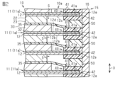
- FIG. 2 is an enlarged cross-sectional view of a part of the power storage device in FIG. 1.
- FIG. 2 is a top view of electrodes included in the power storage device of FIG. 1.
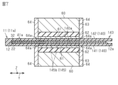
- FIG. 3 is a cross-sectional view for explaining a welding process to a first target part in an electrode manufacturing method of an embodiment.
- 5 is a sectional view taken along line 5-5 in FIG. 4.
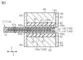
- FIG. 5 is a sectional view taken along line 6-6 in FIG. 4.
- FIG. FIG. 7 is a cross-sectional view for explaining a welding step to a second target part in the electrode manufacturing method of one embodiment.
- FIG. 7 is a cross-sectional view for explaining a welding step for a third target part in the electrode manufacturing method of one embodiment.
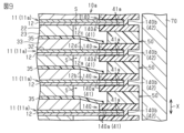
- FIG. 3 is a cross-sectional view for explaining the formation of a sealing part in the electrode manufacturing method of one embodiment.
- power storage device 10 includes a stacked body 10a and a sealing body 15.
- the stacked body 10a is formed by stacking a plurality of electrodes 11 between a positive terminal electrode 36 and a negative terminal electrode 37.
- Power storage device 10 is, for example, a lithium ion secondary battery.
- the direction in which the plurality of electrodes 11 are stacked will be simply referred to as the stacking direction X.
- each of the plurality of electrodes 11 includes a current collector 12, a positive electrode active material layer 23, and a negative electrode active material layer 33.
- the current collector 12 has a sheet shape.
- the current collector 12 has a first surface 12a and a second surface 12b that are opposite to each other in the stacking direction X.
- a positive electrode active material layer 23 is provided on the first surface 12a of the current collector 12, and a negative electrode active material layer 33 is provided on the second surface 12b. That is, each of the plurality of electrodes 11 is a bipolar electrode.
- the plurality of electrodes 11 are such that the first surface 12a of the current collector 12 of one of the two electrodes 11 adjacent to each other in the stacking direction are stacked so as to face the second surface 12b of the current collector 12. That is, the plurality of electrodes 11 are stacked such that the positive electrode active material layer 23 of one electrode 11 and the negative electrode active material layer 33 of the other electrode 11 adjacent to each other in the stacking direction X face each other with the separator 35 in between.
- the positive electrode active material layer 23 is formed in the center of the first surface 12a of the current collector 12 in a plan view viewed from the stacking direction X (hereinafter simply referred to as plan view).
- the peripheral edge of the first surface 12a of the current collector 12 in plan view is a positive electrode uncoated portion 12c where the positive electrode active material layer 23 is not provided.
- the positive electrode uncoated portion 12c is arranged so as to surround the positive electrode active material layer 23 in plan view.
- the negative electrode active material layer 33 is formed at the center of the second surface 12b of the current collector 12.
- the peripheral edge of the second surface 12b of the current collector 12 in plan view is a negative electrode uncoated portion 12d where the negative electrode active material layer 33 is not provided.
- the negative electrode uncoated portion 12d is arranged to surround the negative electrode active material layer 33 in plan view.
- the positive electrode active material layer 23 and the negative electrode active material layer 33 are arranged to face each other in the stacking direction X.
- the negative electrode active material layer 33 is formed to be one size larger than the positive electrode active material layer 23.
- the entire region where the positive electrode active material layer 23 is formed is located within the region where the negative electrode active material layer 33 is formed.
- the current collector 12 is configured by integrating a sheet-shaped positive electrode current collector 22 and a negative electrode current collector 32.
- the first surface 12a of the current collector 12 is constituted by one surface of the positive electrode current collector 22, and the second surface 12b is constituted by one surface of the negative electrode current collector 32.
- the positive electrode current collector 22 and the negative electrode current collector 32 are integrated so that the surface of the positive electrode current collector 22 opposite to the first surface 12a is the surface of the negative electrode current collector 32 opposite to the second surface 12b. It may also be done by bonding with.
- the positive electrode current collector 22 and the negative electrode current collector 32 have the same shape in plan view.
- the current collector 12 has a polygonal shape having a plurality of (three or more) sides 12f in plan view. Specifically, the current collector 12 has four sides 12f and is rectangular in plan view. The outer edge 12e of the current collector 12 is composed of four sides 12f. The two sides 12f are also referred to as short sides 12g, and the two sides 12f longer than the short sides 12g are also referred to as long sides 12h. The short side 12g and the long side 12h are over 1 meter. The short side 12g is, for example, 1.2 meters. The long side 12h is, for example, 1.5 meters.
- the positive electrode current collector 22 and the negative electrode current collector 32 serve to keep current flowing through the positive electrode active material layer 23 and the negative electrode active material layer 33 during discharging or charging of the lithium ion secondary battery.
- It is a chemically inert electrical conductor.
- a metal material, a conductive resin material, or a conductive inorganic material may be used as the material constituting the positive electrode current collector 22 and the negative electrode current collector 32.
- the conductive resin material may be, for example, a resin in which a conductive filler is added to a conductive polymer material or a non-conductive polymer material as necessary.
- the positive electrode current collector 22 and the negative electrode current collector 32 may include multiple layers including one or more layers containing a metal material or a conductive resin material.
- the surfaces of the positive electrode current collector 22 and the negative electrode current collector 32 may be coated with a known protective layer.
- the surfaces of the positive electrode current collector 22 and the negative electrode current collector 32 may be metal plated by a known method such as plating.
- the positive electrode current collector 22 and the negative electrode current collector 32 may have the form of, for example, foil, sheet, film, wire, rod, mesh, or clad material.
- the positive electrode current collector 22 and the negative electrode current collector 32 are metal foils
- the positive electrode current collector 22 and the negative electrode current collector 32 are, for example, aluminum foil, copper foil, nickel foil, titanium foil, or stainless steel foil. It's okay.
- the positive electrode current collector 22 and the negative electrode current collector 32 may be alloy foils of the above metals.
- the thickness of the positive electrode current collector 22 and the negative electrode current collector 32 is, for example, 1 to 100 ⁇ m.
- the positive electrode current collector 22 of this embodiment is an aluminum foil.
- the negative electrode current collector 32 of this embodiment is a copper foil.
- the current collectors 12 of the positive terminal electrode 36 and the negative terminal electrode 37, or some of the current collectors 12 of the plurality of electrodes 11 consisting of bipolar electrodes are The thickness of at least one of them may be 100 ⁇ m or more.
- the current collector 12 is not limited to the form in which the positive electrode current collector 22 and the negative electrode current collector 32 are integrated, and may be a single sheet manufactured from a metal material, a conductive resin material, or a conductive inorganic material. It may be a shaped current collector. Further, the current collector 12 may be a single sheet-like current collector in which a coating layer is formed by plating the surface of the sheet-like current collector. In these cases, one current collector 12 is used as the positive electrode current collector 22 and the negative electrode current collector 32.
- the positive electrode active material layer 23 includes a positive electrode active material that can insert and release lithium ions as charge carriers.
- the positive electrode active material may be, for example, a polyanionic compound such as olivine-type lithium iron phosphate (LiFePO 4 ), a lithium composite metal oxide having a layered rock salt structure, or a metal oxide having a spinel structure.
- the positive electrode active material may be any material as long as it can be used as a positive electrode active material of the power storage device 10 such as a lithium ion secondary battery.
- the negative electrode active material layer 33 includes a negative electrode active material that can insert and release charge carriers such as lithium ions.
- the negative electrode active material is not particularly limited as long as it is a single substance, an alloy, or a compound that can insert and release charge carriers such as lithium ions.
- the negative electrode active material may be Li, carbon, a metal compound, an element that can be alloyed with lithium, or a compound thereof.
- Carbon may be, for example, natural graphite, artificial graphite, hard carbon (non-graphitizable carbon), or soft carbon (easily graphitizable carbon).
- the artificial graphite may be, for example, highly oriented graphite or mesocarbon microbeads.
- the element that can be alloyed with lithium may be, for example, silicon or tin.
- the positive electrode active material layer 23 and the negative electrode active material layer 33 may contain components for increasing electrical conductivity, such as a conductive aid, a binder, an electrolyte (such as a polymer matrix, an ion conductive polymer, or a liquid), as necessary. electrolyte) or an electrolyte supporting salt (lithium salt) for increasing ionic conductivity.
- a conductive aid such as a polymer matrix, an ion conductive polymer, or a liquid
- electrolyte such as a polymer matrix, an ion conductive polymer, or a liquid
- electrolyte such as a polymer matrix, an ion conductive polymer, or a liquid
- electrolyte such as a polymer matrix, an ion conductive polymer, or a liquid
- electrolyte such as a polymer matrix, an ion conductive polymer, or a liquid
- electrolyte such as a polymer matrix, an ion conductive polymer, or
- the conductive aid may be, for example, acetylene black, carbon black, or graphite.
- binders include polyvinylidene fluoride, polytetrafluoroethylene, fluorine-containing resins such as fluororubber, thermoplastic resins such as polypropylene and polyethylene, polyimide, imide resins such as polyamideimide, and alkoxysilyl group-containing resins. resins, acrylic resins such as poly(meth)acrylic acid, styrene-butadiene rubber, carboxymethylcellulose, alginates such as sodium alginate, ammonium alginate, water-soluble cellulose ester crosslinkers, or starch-acrylic acid graft polymers. There may be. These binders may be used alone or in combination.
- the solvent or dispersion medium for example, water or N-methyl-2-pyrrolidone is used.
- Power storage device 10 includes a plurality of separators 35. Each separator 35 is arranged between the positive electrode active material layer 23 and the negative electrode active material layer 33. The separator 35 separates the positive electrode active material layer 23 and the negative electrode active material layer 33 to prevent short circuits caused by contact between the two electrodes, while allowing charge carriers such as lithium ions to pass therethrough.
- the separator 35 may be, for example, a porous sheet or nonwoven fabric containing a polymer that absorbs and retains electrolyte.
- the electrolyte impregnated into the separator 35 may be, for example, a liquid electrolyte containing a non-aqueous solvent and an electrolyte salt dissolved in the non-aqueous solvent, or a polymer gel electrolyte containing an electrolyte held in a polymer matrix. In this embodiment, a liquid electrolyte is used as the electrolyte.
- the electrolyte salt of the liquid electrolyte for example, LiClO 4 , LiAsF 6 , LiPF 6 , LiBF 4 , LiCF 3 SO 3 , LiN(FSO 2 ) 2 , LiN(CF 3 SO 2 ) 2 may be used, and others may be used. Any known lithium salt may be used.
- the nonaqueous solvent for example, cyclic carbonates, cyclic esters, chain carbonates, chain esters, and ethers may be used, or other known solvents may be used. Note that two or more of these known solvent materials may be used in combination.
- the material constituting the separator 35 may be, for example, polypropylene, polyethylene, polyolefin, or polyester. Separator 35 may have a single layer structure or a multilayer structure. The multilayer structure may have, for example, at least one of an adhesive layer and a ceramic layer that is a heat-resistant layer.
- the plurality of electrodes 11 are located between the positive terminal electrode 36 and the negative terminal electrode 37.
- the positive terminal electrode 36 includes a current collector 12 and a positive active material layer 23 disposed on the first surface 12a of the current collector 12, except that it does not include a negative active material layer 33. It has the same configuration as the electrode 11.
- the negative terminal electrode 37 includes a current collector 12 and a negative active material layer 33 disposed on the second surface 12b of the current collector 12, except that it does not include a positive active material layer 23. It has the same configuration as the electrode 11.
- the current collector 12 of the positive terminal electrode 36 is located.
- the current collector 12 of the negative terminal electrode 37 is located.
- the second surface 12b of the current collector 12 included in the positive terminal electrode 36 is the first outer surface 32a of the laminate 10a.
- the first outer surface 32a is a first end surface in the stacking direction X of the stacked body 10a.
- the first surface 12a of the current collector 12 included in the negative terminal electrode 37 is the second outer surface 22a of the laminate 10a.
- the second outer surface 22a is a second end surface in the stacking direction X of the stacked body 10a.
- the first outer surface 32a and the second outer surface 22a are planes extending perpendicularly to the stacking direction X.
- each internal space S exists for each set of a positive electrode current collector 22 and a negative electrode current collector 32 adjacent in the stacking direction X.
- Each internal space S is defined by a positive electrode current collector 22 and a negative electrode current collector 32 that are adjacent to each other in the stacking direction X, and a sealing body 15.
- a positive electrode active material layer 23, a negative electrode active material layer 33, a separator 35, and a liquid electrolyte are arranged.
- the liquid electrolyte is a so-called electrolytic solution, and includes, for example, a non-aqueous solvent and an electrolyte salt dissolved in the non-aqueous solvent.
- Power storage device 10 includes a positive current-carrying plate 38 and a negative current-carrying plate 39 .
- the positive electrode current-carrying plate 38 and the negative electrode current-carrying plate 39 are made of a material with excellent conductivity.
- the material constituting the positive electrode current-carrying plate 38 and the negative electrode current-carrying plate 39 may be, for example, aluminum, copper, stainless steel, or other metal materials.
- the laminate 10a is disposed between the positive current-carrying plate 38 and the negative current-carrying plate 39 in the stacking direction X.
- the positive electrode current-carrying plate 38 is electrically connected to the first outer surface 32a of the laminate 10a.
- the negative electrode current-carrying plate 39 is electrically connected to the second outer surface 22a of the laminate 10a.
- Each of the positive electrode current-carrying plate 38 and the negative electrode current-carrying plate 39 is provided with a terminal (not shown).
- the power storage device 10 performs charging and discharging through terminals provided on the positive electrode current-carrying plate 38 and the negative electrode current-carrying plate 39.
- the sealing body 15 is arranged so as to surround the positive electrode active material layer 23 and the negative electrode active material layer 33 of the plurality of electrodes 11, the positive electrode terminal electrode 36, and the negative electrode terminal electrode 37 when viewed from the stacking direction X.
- the electrode 11, the positive terminal electrode 36, and the negative terminal electrode 37 may be simply referred to as the electrode 11a.
- the sealing bodies 15 each seal between adjacent current collectors 12 in the stacking direction X.
- the sealing body 15 has a plurality of seal portions 40 welded to each of the current collectors 12 of the plurality of electrodes 11a. All of the plurality of seal parts 40 are made of resin. Each seal part 40 has two first seal parts 41 and a second seal part 42. The first seal portion 41 is formed between a first surface 12a of the current collector 12 of one of the electrodes 11a adjacent to each other in the stacking direction X and a second surface 12b of the current collector 12 of the other electrode 11a. This is the part located in between. That is, the first seal portion 41 is arranged inside the outer edge 12e of the current collector 12 when viewed from the stacking direction X.
- the two first seal parts 41 are arranged on both sides (the first surface 12a and the second surface 12b) of the current collector 12, respectively.
- Each first seal portion 41 is arranged continuously along the four sides 12f.
- the seal part 40 has two first seal parts 41 arranged on both sides of the current collector 12 along the side 12f.
- Each seal portion 40 has a welded portion 41a welded to the current collector 12.
- the welded portion 41a is located in the first seal portion 41 at the boundary between the first surface 12a and the second surface 12b.
- the first seal portion 41 is welded to each of the positive electrode uncoated portion 12c and the negative electrode uncoated portion 12d via the welded portion 41a.
- the seal portion 40 is welded to the first surface 12a and the second surface 12b of the current collector 12 of the corresponding electrode 11a via the weld portion 41a.
- the first seal portion 41 located on the positive electrode uncoated portion 12c is arranged to surround the positive electrode active material layer 23.
- the first seal portion 41 located on the negative electrode uncoated portion 12d is arranged to surround the negative electrode active material layer 33.
- the first seal portion 41 has a rectangular frame shape. That is, the rectangular frame-shaped first seal portion 41 is a member having a predetermined width that continuously surrounds the positive electrode active material or the negative electrode active material in plan view.
- the second seal portion 42 is a portion extending outward from the first seal portion 41 beyond the outer edge 12e of the current collector 12. More specifically, the second seal portion 42 is a portion located outside the outer edge 12e of the current collector 12 when viewed from the stacking direction X. The second seal portion 42 is arranged so as to surround the current collector 12 when viewed from the stacking direction X. The second seal portion 42 has a rectangular frame shape. The second seal portion 42 covers the end surface connecting the first surface 12a and the second surface 12b of the current collector 12. The second seal portion 42 connects the outer circumferential portion of the first seal portion 41 located on the positive electrode uncoated portion 12c to the outer circumferential portion of the first seal portion 41 located on the negative electrode uncoated portion 12d.
- the sealing body 15 has a plurality of spacer parts 50.
- Each spacer section 50 is adjacent to the first seal section 41 and the second seal section 42 in the stacking direction X.
- Each spacer section 50 is located between the seal sections 40 provided on two adjacent electrodes 11 in the stacking direction X.
- the spacer section 50 is arranged to surround the positive electrode active material layer 23 and the negative electrode active material layer 33.
- the spacer portion 50 has a rectangular frame shape.
- the spacer portion 50 is made of resin.
- the spacer part 50 is not welded to the first seal part 41. Therefore, the spacer portion 50 is not welded to the current collector 12. Both surfaces of the spacer section 50 in the stacking direction X may be in contact with the first seal section 41 or may be apart from the first seal section 41 .
- the first seal portion 41 and the spacer portion 50 are located between adjacent current collectors 12 in the stacking direction X.
- the first seal part 41 and the spacer part 50 connect the positive electrode current collector 22 of one current collector 12 and the positive electrode current collector 22 of the other current collector 12 among the two current collectors 12 adjacent in the stacking direction X.
- the two are insulated. In this way, the seal portion 40 and the spacer portion 50 suppress short circuit between the positive electrode current collector 22 and the negative electrode current collector 32.
- the spacer portion 50 is welded to at least a portion of the second seal portion 42 adjacent in the stacking direction X. Thereby, the seal portion 40 and the spacer portion 50 are integrated. A region of a predetermined width from the outer edge of the spacer portion 50 is welded to a region of a predetermined width from the outer edge of the second seal portion 42 .
- the sealing body 15 has a sealing part 16, and the sealing part 16 includes a spacer part 50 and a second seal part 42 that are welded to each other. In the sealing part 16, the spacer part 50 and the second seal part 42 are compatible with each other.
- the sealing part 16 has a cylindrical shape extending in the stacking direction X. The sealing portion 16 surrounds the plurality of current collectors 12 from the outside of the stacked body 10a.
- the sealing part 16 seals the internal space S between the current collectors 12 adjacent in the stacking direction X. Sealing portion 16 can suppress moisture from entering internal space S from the outside of power storage device 10 . Sealing portion 16 can suppress leakage of the liquid electrolyte accommodated in internal space S to the outside of power storage device 10 .
- Electrode manufacturing method Next, a method for manufacturing the electrode 11a will be explained. Although the following explanation will be given using the electrode 11, the positive terminal electrode 36 and the negative terminal electrode 37 are also manufactured in the same manner.
- the electrode 11 is manufactured by welding the sealing member 140 to the current collector 12 using the jig 60.
- the positive electrode active material layer 23 is arranged on the first surface 12a
- the negative electrode active material layer 33 is arranged on the second surface 12b. That is, the sealing member 140 is welded to the current collector 12 having active material layers arranged on both sides.
- the manufactured electrode 11 includes a current collector 12 , an active material layer provided on the surface of the current collector 12 , and a seal member 140 welded to the surface of the current collector 12 .
- the seal member 140 Prior to welding the seal member 140 to the current collector 12, the seal member 140 is placed on the current collector 12 (placement step).
- the seal member 140 is made of resin.
- separate seal members 140 first seal member 141, second seal member 142 are arranged on both sides of the current collector 12, that is, on the first surface 12a and the second surface 12b.
- the sealing member 140 is temporarily attached to the current collector 12 by performing spot welding (point welding) using ultrasonic waves or heat. It may be fixed (temporarily welded).
- the seal member 140 placed on the first surface 12a is the first seal member 141.
- the first seal member 141 is separated from the positive electrode active material layer 23.
- the seal member 140 placed on the second surface 12b is the second seal member 142.
- the second seal member 142 is separated from the negative electrode active material layer 33.
- the current collector 12 is sandwiched between the first seal member 141 and the second seal member 142 from both sides in the thickness direction of the current collector 12 .
- Each seal member 140 includes a protrusion 140b that protrudes from the outer edge 12e of the current collector 12.
- the protruding portion 140b is a portion that does not overlap the current collector 12 when viewed from the direction in which the current collector 12 and the seal member 140 are stacked.
- the protrusion 140b of the first seal member 141 and the protrusion 140b of the second seal member 142 are separated from each other.
- a portion of the seal member 140 disposed on both sides of the current collector 12 is referred to as a main body portion 140a.
- the main body portion 140a is a portion that overlaps the current collector 12 when viewed from the direction in which the current collector 12 and the seal member 140 are stacked.
- Each of the first seal member 141 and the second seal member 142 includes a main body portion 140a and a protrusion portion 140b.
- the protruding portion 140b extends from the main body portion 140a. That is, when viewed from the direction in which the current collector 12 and the sealing member 140 are stacked, each sealing member 140 stacks the current collector so that it has both a portion that overlaps with the current collector 12 and a portion that does not overlap with the current collector 12. It is located on 12.
- each sealing member 140 has a strip shape and extends in the longitudinal direction along the side 12f on which it is arranged, and the direction intersecting the side 12f is the transversal direction (width direction). More specifically, the plurality of seal members 140 are arranged along the two long sides 12h and the two short sides 12g of the current collector 12, respectively. In the arrangement step, separate seal members 140 are arranged on the two sides 12f, respectively.
- the seal members 140 arranged along each short side 12g are also referred to as short side seal members 144.
- the seal members 140 arranged along each long side 12h are also referred to as long side seal members 143.
- Each of the long side sealing member 143 and the short side sealing member 144 includes a first sealing member 141 and a second sealing member 142.
- the direction in which the long side 12h extends is also referred to as a first direction Y.
- the direction in which the short side 12g extends is also referred to as a second direction Z.
- the first direction Y is the direction in which two of the four sides 12f extend
- the second direction Z is the direction in which the remaining two sides of the four sides 12f extend.
- both ends 143a of the long side seal member 143 in the first direction Y are more concentrated than the outer edges 12e of both ends of the current collector 12 in the first direction Y. It protrudes to the outside of the electric body 12.
- Each of the long side sealing members 143 overlaps one long side 12h of the current collector 12 and the ends of the two short sides 12g in the second direction Z.
- the short side seal member 144 extends between the two long side seal members 143 in the second direction Z.
- the short side sealing member 144 may overlap the long side sealing member 143, or may be arranged between the two long side sealing members 143 so as not to overlap with the long side sealing member 143.
- each of the short side sealing members 144 overlaps a portion of both ends of one short side 12g of the current collector 12, on which the long side sealing member 143 overlaps. That is, the short side sealing member 144 and the long side sealing member 143 overlap each other.
- the long side sealing member 143 and the short side sealing member 144 are arranged in a frame shape on each of the first surface 12a and the second surface 12b.
- the first sealing member 141 of the long-side sealing member 143 and the short-side sealing member 144 surrounds the positive electrode active material layer 23 .
- the periphery of the negative electrode active material layer 33 is surrounded by the second seal member 142 of the long side seal member 143 and the short side seal member 144 .
- a jig 60 used for welding the seal member 140 to the current collector 12 is, for example, an impulse sealer having a heating wire.
- the impulse sealer includes a pair of jigs 60 arranged to sandwich the current collector 12 in the thickness direction (direction perpendicular to the first direction Y and the second direction Z).
- the jig 60 includes a heater section 61.
- the heater section 61 is, for example, a metal plate having a built-in heating wire (not shown). By adjusting the amount of current flowing through the heating wire, it is possible to switch between heating and stopping the heating of the heater section 61.
- the heater section 61 is deformable.
- the jig 60 includes a rubber part 62 and a base part 63.
- the rubber portion 62 is made of silicone rubber, for example.
- the rubber portion 62 is located so as to overlap the heater portion 61 in the thickness direction of the current collector 12 .
- the heater section 61 is fixed to the rubber section 62.
- the rubber portion 62 is compressible and deformable.
- the base portion 63 is made of metal, for example.
- a rubber portion 62 is located between the base portion 63 and the heater portion 61. Thereby, the rubber portion 62 insulates the base portion 63 and the heater portion 61.
- the rubber portion 62 suppresses heat transfer from the heater portion 61 to the base portion 63.
- the rubber portion 62 is fixed to a base portion 63. Thereby, the heater part 61, the rubber part 62, and the base part 63 are integrated with each other.
- the base portion 63 is movable relative to the welding target. For example, by operating an operating device (not shown) by an operator, the position of the base portion 63 relative to the sealing member and current collector foil to be welded is changed. When the position of the base portion 63 relative to the welding target is changed, the heater portion 61 and the rubber portion 62 integrated with the base portion 63 are displaced together with the base portion 63.
- the heater part 61 and the rubber part 62 are rectangular flat plates.
- the longitudinal direction of the heater section 61 and the rubber section 62 is also referred to as the longitudinal direction of the jig 60.
- the lateral direction of the heater section 61 and the rubber section 62 is also referred to as the lateral direction of the jig 60.
- the size of the rubber part 62 in the width direction of the jig 60 is larger than the size of the heater part 61 in the width direction of the jig 60.
- the rubber portion 62 has a rubber protrusion portion 62a that protrudes outward from the end portion 61a of the heater portion 61 in the lateral direction of the jig 60 when viewed from the stacking direction in which the heater portion 61 and the rubber portion 62 overlap.
- the jig 60 has a jig electrode 64.
- the jig electrode 64 is located outside both ends of each of the heater section 61, the rubber section 62, and the base section 63 in the longitudinal direction of the jig 60.
- the jig electrode 64 has a corner 64a.
- the corner portion 64a is curved.
- the contact surface of the heater section 61 to the sealing member 140 and the surface of the jig electrode 64 perpendicular to the longitudinal direction of the jig 60 are smoothly connected via the corner 64a.
- the corner portion 64a is adjacent to the heater portion 61 in the longitudinal direction of the jig 60. In other words, it can be said that the corner portion 64a is located around the heater portion 61.
- the jig 60 can also be said to have a corner 64a.
- the seal member 140 is welded to the current collector 12 using the jig 60 (welding process).
- the jig 60 is brought into surface contact with the target part 145, which is a part of the sealing member 140, and the target part 145 is heated by the jig 60 while being pressed against the current collector 12.
- the target portion 145 of the seal member 140 is a part between both ends of the seal member 140 in the direction in which the side 12f extends.
- the dimension of the side 12f of the target portion 145 in the extending direction is smaller than the dimension of the side 12f of the current collector 12.
- the target portion 145 is heated by the heater portion 61 while being brought into surface contact with the target portion 145 and pressing the target portion 145 against the current collector 12 . Thereby, in the welding step, the target portion 145 is welded to the surface of the current collector 12.
- the size of the target portion 145 is the same as the size of the area where the heater portion 61 contacts the sealing member 140 .
- a sheet material 65 is arranged between the heating surface of the heater section 61 and the current collector 12 and the sealing member 140, and the heater section 61 is connected to the current collector 12 and the sealing member through the sheet material 65.
- the seal member 140 may be heated by pressing against the seal member 140 . Thereby, adhesion of the molten seal member 140 to the heating surface of the heater section 61 can be suppressed.
- the sheet material 65 may be, for example, a base sheet whose surface is coated with a fluororesin having heat resistance, hard adhesion, and slipperiness. Further, the sheet material 65 may be, for example, a heat-resistant base sheet impregnated with a fluorine-based compound such as polytetrafluoroethylene.
- the target portion 145 includes a main body portion 140a and a portion of the protrusion portion 140b. Therefore, in the welding process, the main body portion 140a is welded to the surface of the current collector 12, and parts of the protruding portions 140b of the first seal member 141 and the second seal member 142 are welded to each other.
- the seal member 140 is welded to the current collector 12 while displacing the relative position of the electrode 11 with respect to the jig 60 in the direction in which the side 12f of the current collector 12 extends. conduct.
- the long side seal member 143 is welded to the current collector 12 while the relative position of the electrode 11 with respect to the jig 60 is displaced in the first direction Y.
- Welding of the short side seal member 144 to the current collector 12 is performed while displacing the relative position of the electrode 11 with respect to the jig 60 in the second direction Z.
- the relative position of the electrode 11 with respect to the jig 60 is changed by displacing the electrode 11 in the first direction Y using a moving device (transfer device) such as a belt conveyor or a robot hand.
- a moving device transfer device
- the dimension of the target portion 145 in the direction in which the side 12f extends is also referred to as the dimension L of the target portion 145.
- the dimension L of the target portion 145 is the dimension of the target portion 145 in the first direction Y.
- the dimension L of the target portion 145 is the dimension of the target portion 145 in the second direction Z.
- the dimension L of the target portion 145 is smaller than the long side 12h.
- the dimension L of the target portion 145 is smaller than the short side 12g.
- the upper limit of the dimension L may be 1/2 or less of the length (1.5 meters) of the long side 12h. Further, the lower limit of the dimension L may be one-third or more of the length of the long side 12h in order to suppress the number of welding steps.
- the dimension L of the target portion 145 is 720 mm or less when performing the welding process on the long side sealing member 143 and when performing the welding process on the short side sealing member 144. It is.
- the region where the heater section 61 is located when the long side sealing member 143 is welded to the current collector 12 is referred to as a long side region R1.
- the region where the heater portion 61 is located when the short side sealing member 144 is welded to the current collector 12 is referred to as a short side region R2.
- the long side region R1 and the short side region R2 are illustrated in FIG. 4 by dotted hatching.
- the mutually overlapping portions of the long side sealing member 143 and the short side sealing member 144 are included in the long side region R1 or the short side region R2. Thereby, the mutually overlapping portions of the long side sealing member 143 and the short side sealing member 144 are welded by the welding process.
- the long side region R1 and the short side region R2 overlap each other at both ends 143a of the long side sealing member 143 in the first direction Y and at both ends 144a of the short side sealing member 144 in the second direction Z.
- the welding process is performed multiple times between both ends of the sealing member 140 in the direction in which the side 12f extends.
- a welding process is performed three times between both ends 143a of the long side sealing member 143 in the first direction Y.
- a welding process is performed twice between both ends 144a of the short side seal member 144 in the second direction Z.
- the target portion 145 is a portion of the sealing member 140 that is at least partially displaced from the target portion 145 in the previous welding step in the direction in which the side 12f extends.
- a portion of the target portion 145 in the first direction Y is shifted from the target portion 145 in the previous welding step.
- a portion of the seal member 140 is referred to as a target portion 145.
- a portion of the target portion 145 in the direction in which the side 12f extends overlaps with the target portion 145 in the previous welding step.
- the target part 145 in the first welding process is referred to as the first target part 145a
- the target part 145 in the second welding process is referred to as the second target part.
- the target portion 145 in the third welding process is referred to as a third target portion 145c.
- the second target portion 145b is partially offset from the first target portion 145a in the first direction Y.
- the third target portion 145c is partially offset from the second target portion 145b in the first direction Y.
- the first end portion of the second target portion 145b in the first direction Y overlaps with a part of the first target portion 145a, and the second end portion of the second target portion 145b in the first direction Y overlaps with a part of the first target portion 145a. overlaps with a part of
- the target part 145 in the first welding process is referred to as the first target part 145a
- the target part 145 in the second welding process is referred to as the second target part.
- Section 145b The first target part 145a and the second target part 145b in the welding process performed with the short side seal member 144 are not shown in FIG. 4.
- a part of the target portion 145 overlaps with the target portion 145 in the previous welding process.
- the ends of the first target part 145a and the second target part 145b in the second direction Z partially overlap with each other.
- the electrode 11 in which the sealing member 140 is integrated with the current collector 12 is manufactured.
- electrodes 11 in which the sealing member 140 is integrated with the current collector 12 are successively manufactured.
- the electrode 11 is moved to the jig 60 until the heater part 61 faces the first target part 145a in the thickness direction of the current collector 12. Move relative. At this time, the electrode 11 is arranged so that the first direction Y is along the longitudinal direction of the jig 60. The pair of jigs 60 are arranged to sandwich the current collector 12 in the thickness direction.
- the welding process is performed on seal members 140 placed on both sides of the current collector 12. As the base portion 63 is displaced in the thickness direction of the current collector 12 from the position where the heater portion 61 faces the first target portion 145a, the jig 60 is displaced so as to approach the first target portion 145a.
- the heater part 61 moves to the position where it contacts the first target part 145a of the sealing member 140, the displacement of the base part 63 in the thickness direction of the current collector 12 is stopped, and thus the displacement of the jig 60 is stopped. At this time, the heater section 61 is pressed against the main body section 140a of each of the first seal member 141 and the second seal member 142. The rubber portion 62 may be compressed and deformed as the heater portion 61 presses the seal member 140. In this embodiment, the pair of jigs 60 are moved closer together to sandwich the sealing member 140 and the current collector 12, and in this state, the heater section 61 of each jig 60 is They are pressed against the sealing member 140 and the exposed portion, respectively. Therefore, one of the pair of jigs 60 is also used as a support member that receives the pressing force of the other jig 60.
- the heater part 61 is heated while the first target part 145a presses the heater part 61. Note that the heating of the heater section 61 may be started before or after the heater section 61 is pressed against the seal member 140.
- the heater part 61 heats the first target part 145a while being in surface contact with the first target part 145a.
- the corner portion 64a of the jig 60 also comes into contact with the sealing member 140.
- Heating of the heater part 61 is stopped while the heater part 61 remains pressed against the first target part 145a.
- the seal member 140 is welded to the current collector 12 as the seal member 140 cools.
- a welded part 41a in which the first target part 145a is welded to the surface of the current collector 12 is formed at a boundary position between the seal member 140 and the current collector 12 in the first target part 145a.
- the welding process for the first target portion 145a using the jig 60 is completed.
- the welding process for the first target portion 145a is completed by displacing the jig 60 in the thickness direction of the current collector 12 so that the heater portion 61 is separated from the sealing member 140.
- the welding process for the second target part 145b is performed.
- the electrode 11 is moved in the first direction Y with respect to the jig 60 until the heater part 61 faces the second target part 145b.
- the jig 60 is displaced so as to approach the second target portion 145b.
- the second target part 145b is welded to the current collector 12 in the same way as when the first target part 145a is welded.
- the end of the second target part 145b in the first direction Y overlaps with a part of the first target part 145a. That is, the heater section 61 presses the second target section 145b and a part of the first target section 145a. Therefore, the end of the second target part 145b in the first direction Y overlaps with a part of the welded part 41a formed in the first target part 145a.
- a welded portion 41a in which the second target portion 145b is welded to the surface of the current collector 12 is formed at the boundary between the seal member 140 and the current collector 12 in the second target portion 145b.
- the welding process for the third target part 145c is performed.
- the electrode 11 is moved in the first direction Y with respect to the jig 60 until the heater part 61 faces the third target part 145c.
- the jig 60 is displaced so as to approach the third target portion 145c.
- the heater part 61 moves to the position where it contacts the third target part 145c of the sealing member 140, it is welded to the current collector 12 of the third target part 145c, similarly to when the first target part 145a and the second target part 145b are welded. Perform welding. At this time, the end of the third target portion 145c in the first direction Y overlaps a part of the second target portion 145b. That is, the heater section 61 presses the third target section 145c and a part of the second target section 145b. Therefore, the end of the third target part 145c in the first direction Y overlaps with a part of the welded part 41a formed in the second target part 145b.
- a welded portion 41a in which the third target portion 145c is welded to the surface of the current collector 12 is formed at the boundary between the seal member 140 and the current collector 12 in the third target portion 145c.
- the electrode 11a integrated with the sealing member 140, the separator 35, and the spacer part 50 are sequentially stacked in the stacking direction X. Of the two electrodes 11a adjacent to each other in the stacking direction .
- the seal member 140 and the spacer portion 50 are welded together.
- the seal member 140 and the spacer portion 50 may be welded together without contact using, for example, a welding jig 70.
- the welding jig 70 is, for example, an infrared heater.
- a part of the protruding part 140b of the sealing member 140 and a part of the spacer part 50 are heated and melted by the infrared rays irradiated from the welding jig 70, so that a part of the protruding part 140b and a part of the spacer part 50 are melted. are welded together and integrated.
- a region of a predetermined width from the edge of the protruding portion 140b of the sealing member 140 is welded to a region of a predetermined width from the edge of the spacer portion 50.
- the outer end surface of the laminated resin part formed by laminating the plurality of seal members 140 and the plurality of spacer parts 50 is welded to form the sealing part 16.
- the seal portion 40 is formed, and the seal portion 16 is formed by the second seal portion 42 and the spacer portion 50 that are integrated with each other.
- the positive electrode current collector 22 of the current collector 12 used in this experiment was an aluminum foil, and the negative electrode current collector 32 was a copper foil.
- the positive electrode current collector 22 and the negative electrode current collector 32 are bonded to each other using a conductive adhesive made of a polyolefin adhesive mixed with carbon as a conductive agent.
- Current collector 12 has a thickness of 65 ⁇ m.
- the sealing member 140 used in the experiment was made of acid-modified low-density polyethylene and had a thickness of 120 ⁇ m.
- the sealing members 140 were welded to both sides of the current collector 12 using an impulse sealer under the conditions that the welding temperature was 195 degrees and the surface pressure during welding was 0.7 MPa or more. In this experiment, if the size of the target portion 145 to which the seal member 140 was welded was 720 mm or less, the current collector 12 did not deform due to welding of the seal member 140 to the current collector 12.
- the jig 60 heats the sealing member 140 while making surface contact with the sealing member 140 and pressing the target portion 145 against the current collector 12 .
- the seal member 140 thermally expands.
- the larger the size of the target portion 145 to be heated by the jig 60 the greater the amount of thermal expansion of the seal member 140.
- the seal member 140 thermally contracts as it cools. The larger the amount of thermal expansion of the sealing member 140, the larger the amount of thermal contraction of the sealing member 140.
- the dimension in the direction in which the side 12f of the target part 145 extends will be the same as the dimension of the long side 12h. If the entire area between both ends 144a of the sealing member 140 in the direction in which the short side 12g extends is the target part 145, the dimension in the direction in which the side 12f of the target part 145 extends is the same as the dimension of the short side 12g. In contrast, the dimension in the extending direction of the side 12f of the target portion 145 in this embodiment is smaller than the side 12f.
- the size of the target part 145 is smaller, so that the amount of thermal expansion of the sealing member 140 is reduced. becomes smaller.
- the amount of thermal expansion of the sealing member 140 becomes smaller, the amount of thermal contraction of the sealing member 140 becomes smaller. Thereby, the contraction force transmitted from the seal member 140 to the current collector 12 due to thermal contraction of the seal member 140 can be reduced. Therefore, deformation of the current collector 12 that occurs when the sealing member 140 is welded to the current collector 12 can be reduced.
- the sealing members 140 are placed on both sides of the current collector 12.
- the welding process is performed on seal members 140 placed on both sides of the current collector 12. Therefore, deformation of the current collector 12 that occurs when the sealing member 140 is welded to both surfaces of the current collector 12 can be reduced.
- the jig 60 has a corner portion 64a that comes into contact with the seal member 140 when the target portion 145 is heated by the heater portion 61.
- the corner portion 64a is curved. Therefore, when the corner 64a comes into contact with the sealing member 140, the occurrence of local swelling of the sealing member 140 due to the sealing member 140 being pushed by the corner 64a can be reduced. If there is a local bulge in the sealing member 140, the dimensional tolerance in the stacking direction X of the power storage device 10 after the sealing member 140 is stacked may increase due to the bulging. According to this embodiment, such an increase in tolerance can be suppressed.
- the dimension of the target portion 145 in the extending direction of the side 12f is 720 mm or less. Therefore, deformation of the current collector 12 that occurs when the sealing member 140 is welded to the current collector 12 can be further reduced.
- the welding process is performed by heating the target portion 145 with the jig 60 while bringing the jig 60 into surface contact with the target portion 145 .
- the number of times the welding process is performed between both ends 143a of the seal member 140 in the first direction Y may be two times, or four or more times.
- the number of times the welding process is performed between both ends 144a of the seal member 140 in the second direction Z may be three or more times.
- the welding process may be performed a different number of times between both ends 143a of the seal member 140 in the first direction Y and between both ends 144a of the seal member 140 in the second direction Z, or the welding process may be performed the same number of times.
- a welding step may also be performed.
- the dimensions of the target portion 145 in the first direction Y are different from each other in all or some of the welding processes. It's okay.
- the dimensions of the target portion 145 in the second direction Z are different from each other in all or some of the welding processes. Good too.
- the dimension of the target part 145 in the first direction Y is 720 mm or more. It can be large.
- the size of the target portion 145 in the second direction Z is larger than 720 mm. It's okay. Even in this case, the deformation of the current collector 12 that occurs when the sealing member 140 is welded to the current collector 12 is greater than the case where the entire sealing member 140 is manufactured in one welding process with the target portion 145. can be reduced.
- the corner portion 64a is not limited to a part of the jig electrode 64.
- the corner portion 64a may be a part of the heater portion 61.
- the corner portion 64a in this case is also located around the heater portion 61.
- the corner portion 64a does not need to be curved.
- the target part 145 is the same as the target part 145 in the previous welding process. They don't have to overlap.
- the target part 145 overlaps with the target part 145 in the previous welding process. It doesn't have to be.
- the target portion 145 in the first welding process does not include both ends of the seal member 140 in the direction in which the side 12f extends.
- the target portion 145 in the second and subsequent welding steps includes both ends of the sealing member 140 in the direction in which the side 12f extends.
- the welding process performed on the seal member 140 disposed on the first surface 12a of the current collector 12 and the welding process performed on the seal member 140 disposed on the second surface 12b are performed at different timings. It's okay to be hurt.
- a welding step may be performed on the arranged seal member 140.
- the sealing member 140 may be welded only to one side of the current collector 12 by performing the placement process and the welding process only to one side of the current collector 12.
- the dimension of the short side 12g is not limited to, for example, 1.2 meters.
- the dimension of the long side 12h is not limited to 1.5 meters.
- the dimension of the short side 12g may be less than 1 meter.
- the expression “at least one” used in this specification means “one or more” of the desired options.
- the expression “at least one” as used herein means “only one option” or “both of the two options” if the number of options is two.
- the expression “at least one” as used herein means “only one option” or “any combination of two or more options” if there are three or more options. means.
- the shape of the current collector 12 in plan view is not limited to a rectangular shape.
- the current collector 12 may have a polygonal shape having a plurality of sides 12f including a side 12f exceeding 1 meter in plan view.
- the power storage device 10 may include a restraining member that restrains the stacked body 10a.
- the restraining member applies a restraining load in the stacking direction X to the region where the positive electrode active material layer 23 and the negative electrode active material layer 33 overlap when the stacked body 10a is viewed from the stacking direction X.
- the restraint member may include, for example, restraint plates disposed at both ends of the stacked body 10a in the stacking direction X, and a fastening member made of bolts and nuts that fasten the restraint plates to each other. In the case of this restraining member, the restraining plates are biased in a direction toward each other by the fastening member, thereby applying a restraining load in the stacking direction X to the stacked body 10a.
- the heater section 61 may be a separate device from the jig 60. In this case, the jig 60 does not need to include the heater section 61.
- the heater section 61 may be a non-contact heating device that heats the target section 145 without contacting the target section 145, such as an infrared heater. Then, at the same time as pressing the target part 145 with the jig 60, or before or after the pressing, heating of the target part 145 by a heating device (heater section 61) separate from the jig 60 may be started. good.
- the jig 60 may press only the target portion 145 one after another, or may press a wider area including at least the target portion 145.
- the portions that will become the target portion 145 may be sequentially heated.
- the heater section 61 that is separate from the jig 60 may be moved, or the direction of heat radiation from the heater section 61 may be changed.
- the heater section 61 may have a plurality of divided heating sections, and the heating area may be sequentially changed by switching the heating section that performs heating.
- a method for manufacturing an electrode comprising: A current collector having a polygonal shape having at least one side exceeding 1 meter in plan view, an active material layer provided on the surface of the current collector, and one or more welded to the surface of the current collector. a sealing member, and the manufacturing method includes a step of arranging the sealing member on the surface of the current collector along the side, and a dimension of the sealing member in the direction in which the side extends is the side.
- a welded part is formed in which the target part is welded to the surface of the current collector.
- a welding step the welding step is performed multiple times between both ends of the sealing member in the direction in which the side extends, and in the second and subsequent welding steps, A method for manufacturing an electrode, wherein the target portion is a portion of the sealing member that is at least partially displaced from the target portion in the welding step.
- the sealing member is arranged on both sides of the current collector, and the welding step is performed on the sealing members arranged on both sides of the current collector, [1] Method of manufacturing the described electrode.
- the jig includes a heater part that heats the target part while in surface contact with the target part, and a seal member located around the heater part when the heater part heats the target part. and a corner in contact with the electrode, the corner being curved, the method for manufacturing an electrode according to any one of [1] to [3].
Landscapes
- Chemical & Material Sciences (AREA)
- Chemical Kinetics & Catalysis (AREA)
- Electrochemistry (AREA)
- General Chemical & Material Sciences (AREA)
- Engineering & Computer Science (AREA)
- Materials Engineering (AREA)
- Manufacturing & Machinery (AREA)
- Composite Materials (AREA)
- Battery Electrode And Active Subsutance (AREA)
Abstract
Description
上記方法によれば、2回目以降の溶着工程において、辺の延びる方向の対象部の一部は前回の溶着工程での対象部と重なる。そのため、溶着工程を行う際に、治具に対する対象部の辺の延びる方向における相対位置が本来の位置からずれたとしても、対象部における前回の溶着工程での対象部と辺の延びる方向に重なる部分が増減するだけになる。これにより、複数の対象部の間で集電体へ溶着しない部分が生じにくい。したがって、集電体に対するシール部材の溶着不良を低減できる。
上記方法によれば、辺の延びる方向の対象部の寸法は720mm以下である。そのため、シール部材の集電体への溶着時に生じる集電体の変形をより低減できる。
<蓄電装置>
図1に示すように、蓄電装置10は、積層体10aと、封止体15と、を備える。積層体10aは、正極終端電極36と負極終端電極37との間に、複数の電極11を積層することにより形成される。蓄電装置10は、例えばリチウムイオン二次電池である。以下では、複数の電極11が積層された方向を単に積層方向Xという。
図1及び図2に示すように、複数の電極11の各々は、集電体12と、正極活物質層23と、負極活物質層33と、を備える。集電体12はシート状である。集電体12は、積層方向Xにおいて互いに逆向きの第1面12aと、第2面12bと、を有している。集電体12の第1面12aには正極活物質層23が設けられるとともに、第2面12bには負極活物質層33が設けられている。すなわち、複数の電極11の各々は、バイポーラ電極である。積層体10aにおいて、複数の電極11は、積層方向Xにおいて互いに隣り合う2つの電極11のうちの一方の電極11の集電体12の第1面12aが、セパレータ35を挟んで他方の電極11の集電体12の第2面12bと対向するように積層されている。つまり、複数の電極11は、積層方向Xに隣り合う一方の電極11の正極活物質層23と他方の電極11の負極活物質層33とがセパレータ35を挟んで対向するように積層される。
本実施形態においては、集電体12はシート状の正極集電体22と負極集電体32とを一体化させることで構成されている。集電体12の第1面12aは正極集電体22の一面によって構成され、第2面12bは負極集電体32の一面によって構成される。正極集電体22及び負極集電体32の一体化は、第1面12aとは反対側の正極集電体22の面が、第2面12bとは反対側の負極集電体32の面と接着されることにより行われてもよい。正極集電体22と負極集電体32とは、平面視での形状が同形状である。
正極活物質層23は、リチウムイオンを電荷担体として吸蔵及び放出可能である正極活物質を含む。正極活物質は、例えば、オリビン型リン酸鉄リチウム(LiFePO4)のようなポリアニオン系化合物、層状岩塩構造を有するリチウム複合金属酸化物、スピネル構造の金属酸化物であってもよい。正極活物質は、リチウムイオン二次電池などの蓄電装置10の正極活物質として使用可能な物質であればよい。
蓄電装置10は、複数のセパレータ35を備える。各セパレータ35は、正極活物質層23と負極活物質層33との間に配置されている。セパレータ35は、正極活物質層23と負極活物質層33とを隔離することで両極の接触による短絡を防止しつつ、リチウムイオンのような電荷担体を通過させる。
積層方向Xにおいて、複数の電極11は、正極終端電極36と負極終端電極37との間に位置している。正極終端電極36は、集電体12と、集電体12の第1面12aに配置された正極活物質層23と、を有しており、負極活物質層33を有さないことを除いて電極11と同様の構成を有する。負極終端電極37は、集電体12と、集電体12の第2面12bに配置された負極活物質層33と、を有しており、正極活物質層23を有さないことを除いて電極11と同様の構成を有する。積層方向Xにおける積層体10aの第1端には、正極終端電極36の集電体12が位置する。積層方向Xにおける積層体10aの第2端には、負極終端電極37の集電体12が位置する。
積層方向Xにおいて隣り合う2つの集電体12の間には、積層方向Xにおいて隣り合う正極集電体22及び負極集電体32の組ごとに、1つの内部空間Sが存在する。各内部空間Sは、積層方向Xにおいて互いに隣り合う正極集電体22及び負極集電体32と、封止体15と、で画定されている。各内部空間S内には、正極活物質層23、負極活物質層33、セパレータ35、及び不図示の液体電解質が配置されている。液体電解質はいわゆる電解液であり、例えば、非水溶媒と、非水溶媒に溶解した電解質塩と、を含む。
蓄電装置10は、正極通電板38及び負極通電板39を備える。正極通電板38及び負極通電板39は、導電性に優れた材料で構成される。正極通電板38及び負極通電板39を構成する材料は、例えば、アルミニウム、銅、ステンレス鋼であってもよいし、その他の金属材料であってもよい。積層体10aは、積層方向Xにおける正極通電板38と負極通電板39との間に配置されている。
封止体15は、積層方向Xから見て、複数の電極11、正極終端電極36及び負極終端電極37の正極活物質層23及び負極活物質層33の周囲を囲むように配置される。以下では、電極11、正極終端電極36、及び負極終端電極37を単に電極11aと記載することがある。封止体15は、積層方向Xにおいて隣り合う集電体12の間をそれぞれ封止する。
次に、電極11aの製造方法について説明する。なお、以下では電極11を用いて説明を行うが、正極終端電極36及び負極終端電極37も同様に製造がなされる。
シール部材140の集電体12への溶着に先だって、シール部材140を集電体12に配置する(配置工程)。シール部材140は樹脂製である。配置工程において、集電体12の両面、すなわち第1面12aと第2面12bとに、それぞれ別個のシール部材140(第1シール部材141,第2シール部材142)が配置される。シール部材140を集電体12の辺12fに沿って延びるように配置した際に、超音波又は熱を用いてスポット溶着(点溶着)を行うことにより、シール部材140を集電体12に仮止め(仮溶着)してもよい。
図5に示すように、集電体12へのシール部材140の溶着に用いる治具60は、例えば電熱線を有するインパルスシーラーである。インパルスシーラーは、集電体12を厚み方向(第1方向Y及び第2方向Zに直交する方向)に挟むように配置される一対の治具60を有する。
図4に示すように、配置工程を行った後に、集電体12に対して治具60を用いてシール部材140を溶着する(溶着工程)。溶着工程においては、シール部材140のうちの一部である対象部145に対して治具60を面接触させつつ、対象部145を集電体12へ押圧しながら治具60によって加熱する。詳細には、シール部材140の対象部145は、辺12fの延びる方向におけるシール部材140の両端部の間の一部である。対象部145の辺12fの延びる方向の寸法は、集電体12の辺12fの寸法よりも小さい。この対象部145に対して、ヒータ部61を面接触させつつ、対象部145を集電体12へ押圧しながらヒータ部61によって加熱する。これにより、溶着工程においては、対象部145が集電体12の表面に溶着される。対象部145の大きさは、ヒータ部61がシール部材140に接触面する領域の大きさと同じである。この溶着工程において、ヒータ部61における加熱面と、集電体12及びシール部材140との間にシート材65を配置して、シート材65を介してヒータ部61を集電体12及びシール部材140に押し付けてシール部材140を加熱してもよい。これにより、ヒータ部61の加熱面に溶融したシール部材140が付着することを抑制できる。
次に、長辺シール部材143に対する溶着工程の詳細について説明する。なお、短辺シール部材144に対する溶着工程の詳細については説明を省略する。以下の長辺シール部材143に対する溶着工程の説明において、「第1方向Y」を「第2方向Z」に読み替えるとともに第3対象部145cに対する溶着を省略することにより、短辺シール部材144に対する溶着工程の説明となる。
図5及び図9に示すように、長辺シール部材143への溶着工程及び短辺シール部材144への溶着工程を行うことにより、シール部材140が集電体12に溶着されると、シール部材140が一体化された電極11aが得られる。なお、溶着工程後の集電体12の表面に溶着したシール部材140の本体部140aが、シール部40の第1シール部41に相当する。溶着工程後の第1シール部材141と第2シール部材142との突出部140bのうちの溶着した部分同士が、シール部40の第2シール部42に相当する。
図9に示すように、シール部材140と一体化された電極11a、セパレータ35、及びスペーサ部50を積層方向Xに順次積層する。積層方向Xに隣り合う2つの電極11aのうち、一方の電極11aに一体化されたシール部材140と、他方の電極11aに一体化されたシール部材140と、の間にスペーサ部50を介在させる。
<対象部の寸法と集電体への変形の発生との関係に関する実験結果>
シール部材140の溶着の対象である対象部145の寸法と、集電体12への変形の発生と、の関係について実験を行った。この実験に用いた集電体12の正極集電体22はアルミニウム箔であり、負極集電体32は銅箔である。実験に用いた集電体12において、正極集電体22と負極集電体32とは互いにポリオレフィン系接着剤に導電助剤としてカーボンを混合した導電性接着剤により貼り合わされている。集電体12は、65μmの厚みを有する。また、実験に用いたシール部材140は、酸変性した低密度ポリエチレンからなり、120μmの厚みを有する。
次に、本実施形態における作用について説明する。
シール部材140を集電体12に溶着させる時、治具60は、シール部材140に面接触しつつ、対象部145を集電体12へ押圧しながらシール部材140を加熱する。治具60からの熱を受けて、シール部材140は熱膨張する。このとき、治具60による加熱対象である対象部145の寸法が大きいほど、シール部材140の熱膨張量は大きくなる。治具60によるシール部材140の加熱が終了すると、シール部材140は冷却に伴って熱収縮する。シール部材140の上記の熱膨張量が大きいほど、シール部材140の熱収縮量は大きくなる。
上記実施形態によれば以下の効果を得ることができる。
(1)シール部材140のうちで辺12fの延びる方向の寸法が辺12fよりも小さい対象部145に対して治具60を面接触させつつ、対象部145を集電体12へ押圧しながら治具60によって加熱する。これにより、対象部145が集電体12の表面に溶着した溶着部41aを形成する溶着工程を行う。そのため、対象部145の辺12fの延びる方向の寸法が辺12fの寸法と同じである場合と比較して、対象部145の寸法が小さくなることにより、シール部材140の熱膨張量が小さくなる。シール部材140の熱膨張量が小さくなることにより、シール部材140の熱収縮量は小さくなる。これにより、シール部材140の熱収縮によってシール部材140から集電体12へ伝わる収縮力を低減できる。したがって、シール部材140の集電体12への溶着時に生じる集電体12の変形を低減できる。
なお、上記実施形態は、以下のように変更して実施することができる。上記実施形態及び以下の変更例は、技術的に矛盾しない範囲で互いに組み合わせて実施することができる。
○ 角部64aは湾曲していなくてもよい。
実施形態及び変更例から把握できる技術的思想について記載する。
[1]電極の製造方法であって、前記電極は、
平面視において、少なくとも1つの1メートルを超える辺を有する多角形状をなす集電体と、前記集電体の表面に設けられた活物質層と、前記集電体の表面に溶着された1以上のシール部材と、備え、前記製造方法は、前記シール部材を前記辺に沿って前記集電体の表面に配置する配置工程と、前記シール部材のうちで前記辺の延びる方向の寸法が前記辺よりも小さい対象部に対して治具を面接触させつつ、前記対象部を前記集電体へ押圧しながら加熱することにより、前記対象部が前記集電体の表面に溶着した溶着部を形成する溶着工程と、を含み、前記溶着工程は、前記辺の延びる方向における前記シール部材の両端部の間で複数回行われ、2回目以降の前記溶着工程においては、前記辺の延びる方向において前回の前記溶着工程での前記対象部から少なくとも一部がずれた前記シール部材の部分を前記対象部とする、電極の製造方法。
Claims (5)
- 電極の製造方法であって、前記電極は、
平面視において、少なくとも1つの1メートルを超える辺を有する多角形状をなす集電体と、
前記集電体の表面に設けられた活物質層と、
前記集電体の表面に溶着された1以上のシール部材と、を備え、
前記製造方法は、
前記シール部材を前記辺に沿って前記集電体の表面に配置する配置工程と、
前記シール部材のうちで前記辺の延びる方向の寸法が前記辺よりも小さい対象部に対して治具を面接触させつつ、前記対象部を前記集電体へ押圧しながら前記対象部を加熱することにより、前記対象部が前記集電体の表面に溶着した溶着部を形成する溶着工程と、を含み、
前記溶着工程は、前記辺の延びる方向における前記シール部材の両端部の間で複数回行われ、2回目以降の前記溶着工程においては、前記辺の延びる方向において前回の前記溶着工程での前記対象部から少なくとも一部がずれた前記シール部材の部分を前記対象部とする、電極の製造方法。 - 前記配置工程において、前記シール部材は前記集電体の両面に配置され、
前記溶着工程は、前記集電体の両面に配置された前記シール部材に対して行われる、
請求項1に記載の電極の製造方法。 - 2回目以降の前記溶着工程において、前記辺の延びる方向の前記対象部の一部は前回の前記溶着工程での前記対象部と重なる、
請求項1又は請求項2に記載の電極の製造方法。 - 前記治具は、前記対象部に対して面接触しつつ前記対象部を加熱するヒータ部と、前記ヒータ部の周囲に位置し、前記ヒータ部による前記対象部の加熱時に前記シール部材に対して接触する角部と、を有し、
前記角部は湾曲している、
請求項1又は請求項2に記載の電極の製造方法。 - 前記辺の延びる方向の前記対象部の寸法は720mm以下である、
請求項1又は請求項2に記載の電極の製造方法。
Priority Applications (3)
| Application Number | Priority Date | Filing Date | Title |
|---|---|---|---|
| US18/857,866 US20250273818A1 (en) | 2022-04-28 | 2023-04-20 | Method for producing electrode |
| JP2024517254A JP7754295B2 (ja) | 2022-04-28 | 2023-04-20 | 電極の製造方法 |
| CN202380036027.3A CN119072810A (zh) | 2022-04-28 | 2023-04-20 | 电极的制造方法 |
Applications Claiming Priority (2)
| Application Number | Priority Date | Filing Date | Title |
|---|---|---|---|
| JP2022-074804 | 2022-04-28 | ||
| JP2022074804 | 2022-04-28 |
Publications (1)
| Publication Number | Publication Date |
|---|---|
| WO2023210482A1 true WO2023210482A1 (ja) | 2023-11-02 |
Family
ID=88518684
Family Applications (1)
| Application Number | Title | Priority Date | Filing Date |
|---|---|---|---|
| PCT/JP2023/015718 Ceased WO2023210482A1 (ja) | 2022-04-28 | 2023-04-20 | 電極の製造方法 |
Country Status (4)
| Country | Link |
|---|---|
| US (1) | US20250273818A1 (ja) |
| JP (1) | JP7754295B2 (ja) |
| CN (1) | CN119072810A (ja) |
| WO (1) | WO2023210482A1 (ja) |
Cited By (1)
| Publication number | Priority date | Publication date | Assignee | Title |
|---|---|---|---|---|
| WO2025115451A1 (ja) * | 2023-11-30 | 2025-06-05 | 株式会社豊田自動織機 | 蓄電モジュール |
Families Citing this family (1)
| Publication number | Priority date | Publication date | Assignee | Title |
|---|---|---|---|---|
| JP7823642B2 (ja) * | 2023-09-15 | 2026-03-04 | トヨタ自動車株式会社 | 二次電池の製造方法 |
Citations (4)
| Publication number | Priority date | Publication date | Assignee | Title |
|---|---|---|---|---|
| JP2005190713A (ja) * | 2003-12-24 | 2005-07-14 | Nissan Motor Co Ltd | バイポーラ電池およびその製造方法。 |
| JP2017168270A (ja) * | 2016-03-15 | 2017-09-21 | 日産自動車株式会社 | リチウムイオン二次電池 |
| JP2020053151A (ja) * | 2018-09-25 | 2020-04-02 | 株式会社豊田自動織機 | 蓄電モジュールの製造方法 |
| JP2020124886A (ja) * | 2019-02-06 | 2020-08-20 | 株式会社豊田自動織機 | 熱溶着装置 |
Family Cites Families (1)
| Publication number | Priority date | Publication date | Assignee | Title |
|---|---|---|---|---|
| JP6984338B2 (ja) * | 2017-11-14 | 2021-12-17 | 株式会社豊田自動織機 | 蓄電モジュールの製造方法 |
-
2023
- 2023-04-20 CN CN202380036027.3A patent/CN119072810A/zh active Pending
- 2023-04-20 WO PCT/JP2023/015718 patent/WO2023210482A1/ja not_active Ceased
- 2023-04-20 JP JP2024517254A patent/JP7754295B2/ja active Active
- 2023-04-20 US US18/857,866 patent/US20250273818A1/en active Pending
Patent Citations (4)
| Publication number | Priority date | Publication date | Assignee | Title |
|---|---|---|---|---|
| JP2005190713A (ja) * | 2003-12-24 | 2005-07-14 | Nissan Motor Co Ltd | バイポーラ電池およびその製造方法。 |
| JP2017168270A (ja) * | 2016-03-15 | 2017-09-21 | 日産自動車株式会社 | リチウムイオン二次電池 |
| JP2020053151A (ja) * | 2018-09-25 | 2020-04-02 | 株式会社豊田自動織機 | 蓄電モジュールの製造方法 |
| JP2020124886A (ja) * | 2019-02-06 | 2020-08-20 | 株式会社豊田自動織機 | 熱溶着装置 |
Cited By (1)
| Publication number | Priority date | Publication date | Assignee | Title |
|---|---|---|---|---|
| WO2025115451A1 (ja) * | 2023-11-30 | 2025-06-05 | 株式会社豊田自動織機 | 蓄電モジュール |
Also Published As
| Publication number | Publication date |
|---|---|
| JP7754295B2 (ja) | 2025-10-15 |
| CN119072810A (zh) | 2024-12-03 |
| JPWO2023210482A1 (ja) | 2023-11-02 |
| US20250273818A1 (en) | 2025-08-28 |
Similar Documents
| Publication | Publication Date | Title |
|---|---|---|
| JP2023087348A (ja) | 蓄電装置の製造方法及び蓄電装置 | |
| WO2022102286A1 (ja) | 蓄電モジュール | |
| JP7754295B2 (ja) | 電極の製造方法 | |
| JP2024037418A (ja) | 蓄電装置及び蓄電装置の製造方法 | |
| JP7559840B2 (ja) | 蓄電セル及び蓄電装置 | |
| US20250201984A1 (en) | Power storage device | |
| WO2023189249A1 (ja) | 蓄電装置 | |
| CN114747061B (zh) | 蓄电装置和蓄电装置的制造方法 | |
| JP7740530B2 (ja) | 電極の製造方法 | |
| KR102961343B1 (ko) | 전극의 제조 방법 | |
| JP2022077634A (ja) | 蓄電装置 | |
| JP2021170486A (ja) | 蓄電セル | |
| JP7745583B2 (ja) | 蓄電デバイスの製造方法 | |
| JP7750402B2 (ja) | 蓄電装置 | |
| JP2021082532A (ja) | 蓄電セルの製造方法 | |
| US20240359268A1 (en) | Method for producing electricity storage device | |
| JP2025097647A (ja) | 蓄電モジュールの製造方法及び蓄電モジュールの製造装置 | |
| JP2025084367A (ja) | 蓄電モジュール製造方法 | |
| WO2025009247A1 (ja) | 蓄電モジュール用電極の製造方法及び蓄電モジュールの製造方法 | |
| JP2025179995A (ja) | 蓄電モジュール製造方法 | |
| JP2025051097A (ja) | 蓄電装置の製造方法 | |
| WO2024053312A1 (ja) | 蓄電装置 | |
| WO2024257457A1 (ja) | 蓄電モジュールの製造方法及び溶着装置 | |
| JP2024162813A (ja) | 蓄電モジュール | |
| JP2022076709A (ja) | 蓄電装置 |
Legal Events
| Date | Code | Title | Description |
|---|---|---|---|
| 121 | Ep: the epo has been informed by wipo that ep was designated in this application |
Ref document number: 23796224 Country of ref document: EP Kind code of ref document: A1 |
|
| ENP | Entry into the national phase |
Ref document number: 2024517254 Country of ref document: JP Kind code of ref document: A |
|
| WWE | Wipo information: entry into national phase |
Ref document number: 18857866 Country of ref document: US |
|
| WWE | Wipo information: entry into national phase |
Ref document number: 202380036027.3 Country of ref document: CN |
|
| NENP | Non-entry into the national phase |
Ref country code: DE |
|
| 122 | Ep: pct application non-entry in european phase |
Ref document number: 23796224 Country of ref document: EP Kind code of ref document: A1 |
|
| WWP | Wipo information: published in national office |
Ref document number: 18857866 Country of ref document: US |