WO2023204253A1 - 導電性シート、配線板および電子機器 - Google Patents
導電性シート、配線板および電子機器 Download PDFInfo
- Publication number
- WO2023204253A1 WO2023204253A1 PCT/JP2023/015645 JP2023015645W WO2023204253A1 WO 2023204253 A1 WO2023204253 A1 WO 2023204253A1 JP 2023015645 W JP2023015645 W JP 2023015645W WO 2023204253 A1 WO2023204253 A1 WO 2023204253A1
- Authority
- WO
- WIPO (PCT)
- Prior art keywords
- conductive
- composition
- conductive composition
- group
- sheet
- Prior art date
- Legal status (The legal status is an assumption and is not a legal conclusion. Google has not performed a legal analysis and makes no representation as to the accuracy of the status listed.)
- Ceased
Links
Classifications
-
- C—CHEMISTRY; METALLURGY
- C08—ORGANIC MACROMOLECULAR COMPOUNDS; THEIR PREPARATION OR CHEMICAL WORKING-UP; COMPOSITIONS BASED THEREON
- C08K—Use of inorganic or non-macromolecular organic substances as compounding ingredients
- C08K3/00—Use of inorganic substances as compounding ingredients
- C08K3/02—Elements
- C08K3/08—Metals
-
- C—CHEMISTRY; METALLURGY
- C09—DYES; PAINTS; POLISHES; NATURAL RESINS; ADHESIVES; COMPOSITIONS NOT OTHERWISE PROVIDED FOR; APPLICATIONS OF MATERIALS NOT OTHERWISE PROVIDED FOR
- C09J—ADHESIVES; NON-MECHANICAL ASPECTS OF ADHESIVE PROCESSES IN GENERAL; ADHESIVE PROCESSES NOT PROVIDED FOR ELSEWHERE; USE OF MATERIALS AS ADHESIVES
- C09J11/00—Features of adhesives not provided for in group C09J9/00, e.g. additives
- C09J11/02—Non-macromolecular additives
- C09J11/04—Non-macromolecular additives inorganic
-
- C—CHEMISTRY; METALLURGY
- C09—DYES; PAINTS; POLISHES; NATURAL RESINS; ADHESIVES; COMPOSITIONS NOT OTHERWISE PROVIDED FOR; APPLICATIONS OF MATERIALS NOT OTHERWISE PROVIDED FOR
- C09J—ADHESIVES; NON-MECHANICAL ASPECTS OF ADHESIVE PROCESSES IN GENERAL; ADHESIVE PROCESSES NOT PROVIDED FOR ELSEWHERE; USE OF MATERIALS AS ADHESIVES
- C09J175/00—Adhesives based on polyureas or polyurethanes; Adhesives based on derivatives of such polymers
- C09J175/04—Polyurethanes
- C09J175/12—Polyurethanes from compounds containing nitrogen and active hydrogen, the nitrogen atom not being part of an isocyanate group
-
- C—CHEMISTRY; METALLURGY
- C09—DYES; PAINTS; POLISHES; NATURAL RESINS; ADHESIVES; COMPOSITIONS NOT OTHERWISE PROVIDED FOR; APPLICATIONS OF MATERIALS NOT OTHERWISE PROVIDED FOR
- C09J—ADHESIVES; NON-MECHANICAL ASPECTS OF ADHESIVE PROCESSES IN GENERAL; ADHESIVE PROCESSES NOT PROVIDED FOR ELSEWHERE; USE OF MATERIALS AS ADHESIVES
- C09J201/00—Adhesives based on unspecified macromolecular compounds
- C09J201/02—Adhesives based on unspecified macromolecular compounds characterised by the presence of specified groups, e.g. terminal or pendant functional groups
-
- C—CHEMISTRY; METALLURGY
- C09—DYES; PAINTS; POLISHES; NATURAL RESINS; ADHESIVES; COMPOSITIONS NOT OTHERWISE PROVIDED FOR; APPLICATIONS OF MATERIALS NOT OTHERWISE PROVIDED FOR
- C09J—ADHESIVES; NON-MECHANICAL ASPECTS OF ADHESIVE PROCESSES IN GENERAL; ADHESIVE PROCESSES NOT PROVIDED FOR ELSEWHERE; USE OF MATERIALS AS ADHESIVES
- C09J7/00—Adhesives in the form of films or foils
- C09J7/30—Adhesives in the form of films or foils characterised by the adhesive composition
-
- C—CHEMISTRY; METALLURGY
- C09—DYES; PAINTS; POLISHES; NATURAL RESINS; ADHESIVES; COMPOSITIONS NOT OTHERWISE PROVIDED FOR; APPLICATIONS OF MATERIALS NOT OTHERWISE PROVIDED FOR
- C09J—ADHESIVES; NON-MECHANICAL ASPECTS OF ADHESIVE PROCESSES IN GENERAL; ADHESIVE PROCESSES NOT PROVIDED FOR ELSEWHERE; USE OF MATERIALS AS ADHESIVES
- C09J9/00—Adhesives characterised by their physical nature or the effects produced, e.g. glue sticks
- C09J9/02—Electrically-conducting adhesives
-
- H—ELECTRICITY
- H01—ELECTRIC ELEMENTS
- H01B—CABLES; CONDUCTORS; INSULATORS; SELECTION OF MATERIALS FOR THEIR CONDUCTIVE, INSULATING OR DIELECTRIC PROPERTIES
- H01B1/00—Conductors or conductive bodies characterised by the conductive materials; Selection of materials as conductors
- H01B1/20—Conductive material dispersed in non-conductive organic material
- H01B1/22—Conductive material dispersed in non-conductive organic material the conductive material comprising metals or alloys
-
- H—ELECTRICITY
- H05—ELECTRIC TECHNIQUES NOT OTHERWISE PROVIDED FOR
- H05K—PRINTED CIRCUITS; CASINGS OR CONSTRUCTIONAL DETAILS OF ELECTRIC APPARATUS; MANUFACTURE OF ASSEMBLAGES OF ELECTRICAL COMPONENTS
- H05K3/00—Apparatus or processes for manufacturing printed circuits
- H05K3/30—Assembling printed circuits with electric components, e.g. with resistors
- H05K3/32—Assembling printed circuits with electric components, e.g. with resistors electrically connecting electric components or wires to printed circuits
-
- C—CHEMISTRY; METALLURGY
- C09—DYES; PAINTS; POLISHES; NATURAL RESINS; ADHESIVES; COMPOSITIONS NOT OTHERWISE PROVIDED FOR; APPLICATIONS OF MATERIALS NOT OTHERWISE PROVIDED FOR
- C09J—ADHESIVES; NON-MECHANICAL ASPECTS OF ADHESIVE PROCESSES IN GENERAL; ADHESIVE PROCESSES NOT PROVIDED FOR ELSEWHERE; USE OF MATERIALS AS ADHESIVES
- C09J2301/00—Additional features of adhesives in the form of films or foils
- C09J2301/30—Additional features of adhesives in the form of films or foils characterized by the chemical, physicochemical or physical properties of the adhesive or the carrier
- C09J2301/314—Additional features of adhesives in the form of films or foils characterized by the chemical, physicochemical or physical properties of the adhesive or the carrier the adhesive layer and/or the carrier being conductive
Definitions
- the present disclosure relates to a conductive composition containing metal powder (A) and a binder (B).
- the invention also relates to conductive sheets, wiring boards, and electronic devices.
- Printed wiring boards mounted inside electronic devices are flexible, but reinforcing plates are sometimes placed in connectors that connect parts to prevent deformation. Although epoxy glass or the like has been used as the reinforcing plate, metal plates have come to be used because of their ability to suppress electromagnetic noise.
- a conductive composition containing resin as a main component is used as a bonding agent to connect a printed wiring board and a metal plate.
- Patent Document 1 discloses that a conductor circuit and a reinforcing plate are connected via a bonding agent layer, and describes that a conductive adhesive containing conductive particles and an adhesive is used as the bonding layer. has been done.
- Patent Document 2 describes a thermosetting resin (A), a curing agent (B), conductive fine particles (C), and a functional material containing at least one element selected from the group consisting of nitrogen, phosphorus, and sulfur.
- a conductive adhesive sheet containing a compound (D) which is at least one selected from the group consisting of a silane coupling agent, a silyl compound, phosphoric acid, and a bisphenol S-type epoxy resin.
- Patent Document 3 describes a resin composition containing a resol type phenol resin having a dimethylene ether bond and a linear polymer having a molecular weight of 1000 or more and having compatibility with the phenol resin, as a conductive composition used for electronic parts etc.
- An electrically conductive composition is disclosed that comprises a solid binder and metal particles comprising Cu powder coated with Ag.
- Patent Document 4 discloses a conductive paste containing a polyurethane prepolymer having an NCO value of 12 to 14% and a viscosity of 1000 to 2000 mPa ⁇ s.
- conductive sheets with a two-layer structure of a conductive layer/protective sheet are often manufactured in roll form and stored.
- the conductive composition adheres to the back surface of the protective sheet during use, ie, so-called blocking (blocking resistance).
- the conductive sheet is used by adhering (temporarily pasting) the first adherend and the conductive composition, then peeling off the protective sheet, and adhering the second adherend to the exposed conductive composition.
- peeling failures such as damage to the protective sheet occur when the protective sheet is peeled off (easy peelability).
- the conductive composition may be stored refrigerated or frozen.
- conductive compositions taken out of refrigerated or frozen storage may form condensation due to moisture in the air. If the bonding operation is performed in the presence of water droplets (including minute water droplets that are invisible to the naked eye) on the surface of the binder, poor bonding may occur. Therefore, the work of pasting onto an adherend cannot be carried out until the moisture evaporates, which causes a decrease in production efficiency (instant nature).
- a conductive sheet is usually temporarily attached to a wiring board and bonded by thermocompression bonding. If removability (reworkability) can be ensured at the stage of temporary attachment to a wiring board, manufacturing yield can be increased, but re-peeling may leave adhesive residue on the adherend, making rework impossible. Further, as wiring boards become thinner, the wiring boards themselves tend to be more easily damaged, and there is also the problem that it is not easy to ensure reworkability at the stage of temporary attachment.
- the present disclosure provides a conductive composition that has excellent metal recovery properties, high adhesive strength and conductivity, prevents adhesion to the protective sheet during storage, and has excellent removability of the protective sheet, water droplet evaporation performance, and reworkability.
- An object of the present invention is to provide a conductive sheet having a material and a wiring board comprising the conductive composition.
- the present disclosure provides the following conductive composition, conductive sheet, wiring board, and electronic device.
- the conductive composition according to the present disclosure is a conductive composition in which a conductive composition containing a metal powder (A) and a binder (B) is disposed on one main surface of a protective sheet (D).
- the conductive composition dissolves and leaves a residue when immersed in the solvent composition (C) at 30°C for 24 hours, the residue containing a metal element,
- the peak density Spd of the surface of the conductive composition on the side not facing the protective sheet (D) is 1,000 to 500,000 pieces/mm 2
- the solvent composition (C) contains the nitrogen-containing organic solvent (c1) in an amount of 5 to 40% by mass based on the total mass of the solvent composition (C), and the basic inorganic compound (c2) in the solvent composition (C).
- [3] The conductive sheet according to [1] or [2], wherein the binder (B) has one or more selected from the group consisting of an ester group, an imide group, an amide group, a urethane group, and a urea group.
- the binder (B) has two or more types selected from the group consisting of an ester group, an imide group, an amide group, a urethane group, and a urea group, according to any one of [1] to [3].
- the conductive composition has a maximum storage modulus (2) of 0.01 to 100 GPa at 0 to 30°C, Any one of [1] to [5], wherein the value ⁇ obtained by dividing the maximum value (2) by the maximum value (1) of the storage modulus of the protective sheet (D) at 0 to 30°C is 0.01 to 30.
- An electronic device comprising the wiring board according to [8].
- a conductive composition comprising: [11]: The conductive composition according to [10], which has adhesive properties. [12]: The conductive composition according to [10] or [11], wherein the binder (B) has one or more selected from the group consisting of an ester group, an imide group, an amide group, a urethane group, and a urea group. thing.
- the binder (B) has two or more types selected from the group consisting of an ester group, an imide group, an amide group, a urethane group, and a urea group, according to any one of [10] to [12].
- conductive composition has two or more types selected from the group consisting of an ester group, an imide group, an amide group, a urethane group, and a urea group, according to any one of [10] to [12].
- the conductive material has excellent metal recoverability, high adhesive strength and conductivity, prevents adhesion with the protective sheet during storage, and has excellent removability of the protective sheet, evaporation of water droplets, and reworkability.
- a conductive sheet having a conductive composition is provided. This makes it possible to provide a wiring board whose resources can be easily recovered.
- the conductive composition of the present disclosure includes a metal powder (A) and a binder (B). This conductive composition was immersed in a solvent composition (C) containing 5 to 40% by mass of a nitrogen-containing organic solvent (c1) and 5 to 40% by mass of a basic inorganic compound (c2) at 30°C for 24 hours. At this time, a part is dissolved and a part is insoluble, and the insoluble portion contains a metal element derived from the metal powder (A). In other words, the conductive composition is dissolved and a residue remains. This residue contains metal elements derived from the metal powder (A).
- dissolving in the present disclosure refers to immersing a target article in the solvent composition (C), bringing the article into contact with the solvent composition (C), and dissolving a part of the article in the solvent composition (C). It is defined as a phenomenon in which the original form is no longer maintained due to melting. That is, it is not necessary that all of the article is dissolved in the solvent composition (C), and insoluble matter (residue) may be present.
- the metal elements contained in the insoluble matter (residue) when the conductive composition of the present disclosure is dissolved in the solvent composition (C) include those derived from the metal powder (A). It is the binder (B) that the solvent composition (C) acts. Due to the decomposition effect of the solvent of the solvent composition (C), the binder (B) is decomposed and dissolved into the solvent composition (C), and the insoluble metal powder (A) is included in the residue, so that the conductive composition Metal powder (A) in objects can be efficiently recovered.
- the conductive layer of the present disclosure dissolves and leaves a residue when immersed in the solvent composition (C) at 30°C for 24 hours, and the metal element derived from the metal powder (A) is dissolved in the residue. including.
- the metal powder (A) is used for the purpose of imparting conductivity to the conductive composition.
- the metal powder (A) is preferably a conductive metal such as gold, platinum, silver, copper, or nickel, or an alloy thereof.
- a conductive metal such as gold, platinum, silver, copper, or nickel, or an alloy thereof.
- composite fine particles having a core and a coating layer formed of a material having higher conductivity than the core and covering the surface of the core may be used.
- Composite fine particles are preferable from the viewpoint of cost reduction.
- the core is preferably a conductive metal or an alloy thereof, and more preferably selected from nickel, silica, and copper.
- the coating layer may be any material as long as it has conductivity, and is preferably a conductive metal or a conductive polymer. Examples of the conductive metal include gold, platinum, silver, tin, manganese and indium, and alloys thereof. Among these, silver is preferred from the viewpoint of electrical conductivity.
- the metal powder (A) may be used alone or in combination of two or more.
- the composite fine particles preferably have a coating layer in an amount of 1 to 40 parts by mass, more preferably 5 to 30 parts by mass, based on 100 parts by mass of the core. Coating with 1 to 40 parts by mass can further reduce costs while maintaining conductivity. Note that in the composite fine particles, it is preferable that the coating layer completely covers the core. However, in reality, a part of the nuclear body may be exposed. Even in such a case, if 70% or more of the surface area of the core is covered with a conductive substance, conductivity can be easily maintained.
- the shape of the metal powder (A) is not limited as long as the desired conductivity can be obtained.
- spherical, flake-like, leaf-like, dendritic (dendritic)-like, plate-like, needle-like, rod-like, grape-like, and irregular block shapes are suitable.
- a spherical shape and a dendritic shape are more preferable in order to efficiently form a vertical conduction path between the metal reinforcing plate and the wiring board.
- the average particle diameter of the metal powder (A) is preferably 5 to 20 ⁇ m when the metal powder (A) is spherical, dendritic, acicular, rod-shaped, grape-shaped, or irregularly shaped. , more preferably 5.5 to 15 ⁇ m, and even more preferably 6 to 10 ⁇ m.
- an average particle diameter D50 of 5 to 20 ⁇ m both adhesive strength and conductivity can be achieved. Note that the average particle diameter D50 can be determined using a laser diffraction/scattering method particle size distribution measuring device.
- D10 is 1 to 15 ⁇ m
- D90 is 10 to 30 ⁇ m. It is preferable from the viewpoint of achieving both adhesiveness and conductivity.
- D 10 and D 90 can be determined by a laser diffraction/scattering particle size distribution measurement device in the same way as the average particle diameter D 50 .
- D 90 /D 10 is preferably from 1.5 to less than 8.0. Within this range, the filling state of the metal powder (A) in the conductive composition is optimized, and the conductivity is particularly excellent.
- the average particle diameter D50 of the metal powder (A) is preferably 5 to 50 ⁇ m, more preferably 6.5 to 30 ⁇ m, and more preferably 8 to 20 ⁇ m. More preferred. By having an average particle diameter D50 of 5 to 50 ⁇ m, both adhesive strength and conductivity can be achieved.
- D10 is 1 to 25 ⁇ m
- D90 is 10 to 100 ⁇ m, from the viewpoint of achieving both adhesiveness and conductivity. preferred.
- D 90 /D 10 is preferably from 1.5 to less than 8.0. Within this range, the filling state of the metal powder (A) in the conductive composition is optimized, resulting in particularly excellent conductivity.
- the content of the metal powder (A) in the conductive composition is preferably 40 to 90% by mass, more preferably 45 to 80% by mass, and even more preferably 50 to 70% by mass. By adding the above amount, it is possible to achieve both metal recovery performance, adhesive strength, and conductivity.
- the binder (B) serves as a base for the conductive composition and has the function of dispersing and supporting the metal powder (A). Since the binder (B) needs to be decomposed by the solvent composition (C), an organic substance is preferable.
- the composition of the binder (B) is not particularly limited as long as it has the above-mentioned functions, but it preferably contains the resin (b-1).
- the resin (b-1) in the present disclosure is defined as an organic material that is solid, semi-solid, or solidified at room temperature, has a softening or melting range, and has a weight average molecular weight (Mw) of 5,000 or more.
- the specific chemical bonds of the binder (B) are decomposed by the solvent composition (C), which has a strong solvent decomposition action, and the binder (B) can be dissolved in the solvent composition (C).
- the binder (B) has one or more types selected from the group consisting of an ester group, an imide group, an amide group, a urethane group, and a urea group.
- the binder (B) has two or more types selected from the group consisting of an ester group, an imide group, an amide group, a urethane group, and a urea group.
- the binder (B) can be decomposed more efficiently.
- a preferred example is a combination of one or more selected from ester groups, imide groups, amide groups, urea groups, and ester groups and a urethane group.
- the resin (b-1) is not particularly limited in composition, molecular structure, etc. other than the weight average molecular weight (Mw) mentioned above, but one type selected from the group consisting of imide bonds, amide bonds, urethane bonds, and urea bonds. Resins having the above chemical bonds are preferred. Furthermore, from the viewpoint of exhibiting the function of dispersing and supporting the metal powder (A), the resin (b-1) may be a thermosetting resin, a thermoplastic resin, a photocurable resin such as an ultraviolet curable resin, a natural resin, or an elastomer. The resin (b-1) is preferably a thermosetting resin (b-2) from the viewpoint of imparting excellent adhesiveness to the conductive composition.
- thermosetting resin (b-2) is one of the resins (b-1) that has thermosetting properties.
- Thermosetting is defined as "polymerization and/or crosslinking reactions caused by heat, resulting in an irreversible increase in elastic modulus.”
- thermosetting resin (b-2) has a reactive functional group
- thermosetting property may be expressed by reacting the reactive functional groups with each other; It may be expressed by the reaction of reactive functional groups incorporated into b-2) and the curing agent (H) described below.
- thermosetting resin (b-2) examples include epoxy resin, phenol resin, polyacrylic resin, polyester resin, polyurethane resin, polyamide resin, polyimide resin, polyamideimide resin, urea resin, polyurethane urea resin, melamine resin, Examples include polyolefin resins. Among these, it is preferable that the thermosetting resin (b-2) has one or more types selected from the group consisting of an ester group, an imide group, an amide group, a urethane group, and a urea group. An imide bond, an amide bond, a urethane bond, and a urea bond can achieve strong adhesion when the lone pair of nitrogen atoms contained in the bond interacts with the adherend.
- thermosetting resin (b-2) has two or more types selected from the group consisting of an ester group, an imide group, an amide group, a urethane group, and a urea group, the above-mentioned effect of improving adhesiveness is further enhanced. be able to.
- the binder (B) may further contain a curing agent (H).
- the curing agent (H) in the present disclosure is a substance that promotes or regulates a curing reaction, and is defined as a substance having a molecular weight or weight average molecular weight (Mw) of less than 5,000.
- a curing reaction is defined as "polymerizing and/or crosslinking a prepolymer or polymer composition by means such as heating, radiation, or a catalyst to irreversibly increase the elastic modulus.”
- the binder (B) of the present disclosure contains a curing agent (H) from the viewpoint of forming polymerization and/or crosslinking by stimulation such as heat in the binder (B) and developing strong adhesiveness to the conductive composition. It is preferable to include.
- the curing agent (H) may be appropriately selected from known compounds that exhibit curability in combination with the thermosetting resin (b).
- Examples of the curing agent (H) include epoxy compounds, oxetane compounds, episulfide compounds, aziridine compounds, isocyanate compounds, amine compounds, isocyanate compounds, imidazole compounds, and acid anhydrides.
- epoxy compound for example, a glycidyl ether type epoxy compound, a glycidyl amine type epoxy compound, a glycidyl ester type epoxy compound, and a cycloaliphatic (alicyclic type) epoxy compound are preferable.
- Examples of the glycidyl ether type epoxy compounds include bisphenol A type epoxy compounds, bisphenol F type epoxy compounds, bisphenol S type epoxy compounds, bisphenol AD type epoxy compounds, cresol novolac type epoxy compounds, phenol novolac type epoxy compounds, a-1 - Naphthol novolac type epoxy compound, bisphenol A type novolac type epoxy compound, dicyclopentadiene type epoxy compound, tetrabromobisphenol A type epoxy compound, brominated phenol novolac type epoxy compound, tris(glycidyloxyphenyl)methane, tetrakis(glycidyloxy) phenyl)ethane.
- Examples of the glycidylamine type epoxy compound include tetraglycidyldiaminodiphenylmethane, triglycidylpara-aminophenol, triglycidylmethaminophenol, and tetraglycidylmethaxylylenediamine.
- Examples of the glycidyl ester type epoxy compound include diglycidyl phthalate, diglycidyl hexahydrophthalate, and diglycidyl tetrahydrophthalate.
- cycloaliphatic (alicyclic type) epoxy compound examples include epoxycyclohexylmethyl-epoxycyclohexane carboxylate and bis(epoxycyclohexyl) adipate.
- Oxetane compounds include, for example, 1,4-bis ⁇ [(3-ethyloxetan-3-yl)methoxy]methyl ⁇ benzene, 3-ethyl-3- ⁇ [(3-ethyloxetan-3-yl)methoxy]methyl ⁇ Oxetane, 1,3-bis[(3-ethyloxetan-3-yl)methoxy]benzene, 4,4'-bis[(3-ethyl-3-oxetanyl)methoxymethyl]biphenyl, (2-ethyl-2 -Oxetanyl) esterified product of ethanol and terephthalic acid, (2-ethyl-2-oxetanyl) ether compound of ethanol and phenol novolac resin, (2-ethyl-2-oxetanyl) ester of ethanol and polyhydric carboxylic acid compound Examples include chemical compounds.
- Episulfide compounds include, for example, bis(1,2-epithioethyl) sulfide, bis(1,2-epithioethyl) disulfide, bis(2,3-epithiopropyl) sulfide, bis(2,3-epithiopropylthio)methane.
- aziridine compound examples include trimethylolpropane-tri-a-2-aziridinylpropionate, tetramethylolmethane-tri-a-2-aziridinylpropionate, N,N'-diphenylmethane-4,4' -bis(1-aziridinecarboxamide) and N,N'-hexamethylene-1,6-bis(1-aziridinecarboxamide).
- amine compound examples include diethylenetriamine, triethylenetetramine, methylenebis(2-chloroaniline), methylenebis(2-methyl-6-methylaniline), 1,5-naphthalene diisocyanate, and n-butylbenzyl phthalic acid.
- isocyanate compound examples include tolylene diisocyanate, diphenylmethane diisocyanate, hexamethylene diisocyanate, isophorone diisocyanate, xylylene diisocyanate, dicyclohexylmethane diisocyanate, 1,5-naphthalene diisocyanate, tetramethylxylylene diisocyanate, and trimethylhexamethylene diisocyanate.
- imidazole compound examples include 2-methylimidazole, 2-heptadecylimidazole, 2-phenyl-4-methylimidazole, and 1-cyanoethyl-2-undecylimidazolium trimellitate.
- acid anhydride examples include tetrahydrophthalic anhydride, dodecenylsuccinic anhydride, methylnadic anhydride, trimellitic anhydride, and pyromellitic anhydride.
- the content of the curing agent (H) is preferably 1 to 70 parts by mass, more preferably 3 to 50 parts by mass, based on 100 parts by mass of the thermosetting resin (b-2). , more preferably 3 to 30 parts by mass.
- the conductive composition can be brought into a B-stage cured state.
- B-stage curing is a method of partially causing a curing reaction of the curing agent (H) contained in the conductive composition by heating it at a predetermined temperature and time.
- the strength can be increased while maintaining the adhesive force of the conductive composition, and the blocking resistance can be improved by increasing the elasticity of the conductive composition.
- the content of the curing agent (H) to 70 parts by mass or less, formation of an excessive crosslinked structure is suppressed when the conductive composition is cured, and the binder ( The solubility of B) can be increased.
- the step of heating the conductive composition and adhering it to the adherend is preferably hot pressing. Adding pressure treatment improves adhesion to adherends.
- the hot pressing conditions can be appropriately selected depending on the composition of the conductive composition and the material, size, and shape of the adherend. For example, 130 to 200°C, 1 to 10 MPa, and 3 to 60 minutes are preferable.
- the content of the binder (B) is preferably 10 to 60% by mass based on the total solid content of the conductive composition from the viewpoint of excellent adhesiveness to metal plates and printed circuit boards.
- the conductive composition of the present disclosure preferably has voids.
- the presence of voids in the conductive composition promotes penetration of the solvent composition (C) and improves metal recovery. Any known method can be used to adjust the presence or absence of voids and the porosity, but by using dendritic metal powder as the metal powder (A), voids can be created relatively easily. I can do it.
- the porosity of the conductive composition is preferably 0.5 to 60%.
- the porosity is more preferably 1.0 to 30%.
- porosity means the area ratio of voids derived from a microscopic image of a cross section of a conductive composition.
- the specific calculation method is as follows. The cut surface of the conductive composition is observed using a microscope such as a scanning electron microscope (SEM) or a laser microscope as appropriate. When the cut surface is observed vertically using a microscope, there is a contrast difference between the conductive composition and the voids, and the shape of the voids can be recognized. A cross-sectional image obtained by cutting the conductive composition is binarized into black and white, with the conductive composition portion and the void portion using image analysis software “GIMP2.10.6”. Then, by counting the number of black and white pixels, the ratio of the area of the void is calculated from the ratio of the number of pixels.
- the porosity of the conductive composition can be determined by appropriately using known methods such as using a foaming agent that foams and creates voids due to an arbitrary trigger such as heat, but it also depends on the shape and content of the metal powder (A). It is particularly preferable to control the amount.
- the metal powder (A) is particularly bulky and dendritic, voids that exhibit the effects of the present disclosure are likely to be formed, which is preferable compared to other metal powders.
- the number of voids tends to increase.
- the solvent composition (C) of the present disclosure includes a nitrogen-containing organic solvent (c1) and a basic inorganic compound (c2). From the viewpoint of efficiently exerting the solubility effect of the solvent composition (C) on the binder (B), the solvent composition (C) contains a nitrogen-containing organic solvent (c1) based on the total mass of the solvent composition (C). Contains 5 to 40% by mass. The content of the nitrogen-containing organic solvent (c1) is more preferably 10 to 30% by mass.
- the nitrogen-containing organic solvent (c1) can be used without particular limitation as long as it is an organic solvent containing a nitrogen atom in its molecule.
- N-methyl-2-pyrrolidone normal propyl bromide, ⁇ -butyrolactone, monoethanolamine, diethanolamine, triethanolamine, etc.
- the types can be selected as appropriate depending on the content of the binder (B) to be dissolved. You can choose.
- the solvent composition (C) contains a basic inorganic compound (c2) in the total mass of the solvent composition (C). Contains 5 to 40% by mass. Any substance that exhibits the above-mentioned function may be used without any particular restriction, but basic inorganic compounds (c2) include, for example, sodium hydroxide, potassium hydroxide, ammonium hydroxide, sodium hydrogen carbonate, sodium dihydrogen phosphate, At least one selected from the group consisting of disodium phosphate, trisodium phosphate, potassium dihydrogen phosphate, and tripotassium phosphate is included. From the viewpoint of imparting suitable solubility to the solvent composition (C), the content of the basic inorganic compound (c2) is more preferably 10 to 30% by mass.
- An organic solvent for dilution, an additive that promotes decomposition of the binder (B), and the like may be added as appropriate to the solvent composition (C) from the viewpoint of imparting fluidity. From the viewpoint of facilitating the handling of the solvent composition (C), it is preferable to use low-volatility glycerin.
- the conductive sheet according to the present embodiment is a conductive sheet in which a conductive composition containing a metal powder (A) and a binder (B) is disposed on one main surface (one surface only) of a protective sheet (D). It is a sex sheet.
- the present conductive sheet is a sheet-like article having a conductive composition on the protective sheet (D).
- the conductive composition included in the conductive sheet is a solid substance that is non-flowable at room temperature, and forms a layer with a certain thickness, which is also referred to as a conductive layer. This conductive layer dissolves and leaves a residue when immersed in the solvent composition (C) at 30° C. for 24 hours, and the residue contains a metal element.
- the protective sheet (D) can be appropriately used as long as it is a film that has been subjected to release treatment on one or both sides.
- Examples of the base material of the protective sheet (D) include polyethylene terephthalate, polyethylene naphthalate, polyvinyl fluoride, polyvinylidene fluoride, hard polyvinyl chloride, polyvinylidene chloride, nylon, polyimide, polystyrene, polyvinyl alcohol, and ethylene/vinyl alcohol.
- Plastic sheets such as copolymers, polycarbonates, polyacrylonitrile, polybutene, flexible polyvinyl chloride, polyvinylidene fluoride, polyethylene, polypropylene, polyurethane, ethylene-vinyl acetate copolymers, polyvinyl acetate; glassine paper, high-quality paper, kraft paper, Papers such as coated paper; examples include various nonwoven fabrics, synthetic papers, metal foils, and composite films combining these.
- polyethylene terephthalate and polyethylene naphthalate are preferred from the viewpoint of improving easy peelability.
- the surface of the protective sheet (D) may be subjected to matte treatment if necessary.
- matte treatments include sand mats, etched mats, coating mats, chemical mats, and kneaded mats.
- the protective sheet (D) can be obtained, for example, by applying a release agent to the base material.
- Mold release agents include hydrocarbon resins such as polyethylene and polypropylene, higher fatty acids and their metal salts, higher fatty acid soaps, waxes, animal and vegetable oils, mica, talc, silicone surfactants, silicone oils, silicone resins, and fluorine-based resins. Surfactants, fluororesins, fluorine-containing silicone resins, melamine resins, acrylic resins, etc. are used.
- a method for applying the release agent conventionally known methods such as gravure coating method, kiss coating method, die coating method, lip coating method, comma coating method, blade coating method, roll coating method, knife coating method, spray coating method, This can be done by a bar coat method, a spin coat method, or a dip coat method.
- the maximum storage modulus (1) of the protective sheet (D) at 0 to 30°C is preferably 0.01 to 1000 GPa, more preferably 0.1 to 100 GPa. Since the maximum value (1) of the storage modulus of the protective sheet (D) at 0 to 30°C is 0.01 to 1000 GPa, it is easy to remove the protective sheet (D) from the conductive composition after thermal lamination. The protective sheet (D) can be easily peeled off without being stretched or damaged.
- the maximum value (2) of the storage modulus of the conductive composition (conductive layer) at 0 to 30°C is preferably 0.01 to 100 GPa, more preferably 1 to 10 GPa. Since the highest value (2) of the storage modulus of the conductive composition at 0 to 30°C is within this range, when the protective sheet (D) is peeled off and removed from the conductive composition after thermal lamination, the conductive composition It can be easily peeled off without stretching or breaking.
- the storage modulus of the conductive composition and the protective sheet (D) can be determined using a dynamic viscoelasticity measuring device.
- the value ⁇ obtained by dividing the maximum storage modulus (2) of the conductive composition (conductive layer) at 0 to 30°C by the maximum storage modulus (1) of the protective sheet (D) at 0 to 30°C is , preferably from 0.01 to 30, more preferably from 0.1 to 15.
- ⁇ is 0.01 to 30, the protective sheet (D) can be easily peeled off from the conductive composition after thermal lamination.
- the conductive sheet of the present disclosure has a peak density Spd of 1,000 to 500,000 pieces/mm on the surface of the conductive composition (conductive layer) that does not face the protective sheet (D) (on the non-opposed side). It is 2 .
- the peak density Spd is preferably 10,000 to 300,000 pieces/mm 2 , more preferably 25,000 to 250,000 pieces/mm 2 .
- the peak density Spd of the interface (hereinafter sometimes simply referred to as Spd) is defined in ISO 25178-2:2012, and represents the number of peaks per defined region (unit area).
- the conductive sheet of the present disclosure has an adhesive property that the developed area ratio Sdr of the surface of the conductive composition (conductive layer) on the non-opposing surface not facing the protective sheet (D) is 0.01 to 4. This is preferable from the viewpoint of achieving both high and blocking resistance.
- the conductive sheet is stored or transported in a rolled state. When unwinding a conductive sheet from a roll-shaped conductive sheet, a blocking phenomenon may occur in which the conductive sheet adheres to the back surface of the protective sheet (D).
- the unevenness per defined area can be made dense. Thereby, the contact area between the surface of the conductive composition and the back surface of the protective sheet (D) in the roll-shaped body can be reduced, and both adhesiveness and blocking resistance can be achieved.
- the developed area ratio Sdr (hereinafter sometimes simply referred to as Sdr) of the interface is defined in ISO 25178-2:2012, and is the ratio of the developed area (surface area) of the defined region to the area of the defined region. This is an index that shows whether the amount is increasing. Note that the Sdr of the flat surface is 0 (zero).
- values measured in accordance with ISO 25178-2:2012 are used for the peak density Spd and developed area ratio Sdr.
- measurement data was acquired using a laser microscope (manufactured by Keyence Corporation, VK-X100), and analysis software (ISO 25178-2:2012 surface texture measurement module "VK-H1XR") was used to analyze the acquired measurement data.
- analysis software ISO 25178-2:2012 surface texture measurement module "VK-H1XR”
- it can be calculated by importing it into the analysis application "VK-H1XA” (both manufactured by Keyence Corporation) and executing ISO 25178-2:2012 surface texture measurement.
- the present inventor further found that when the developed area ratio Sdr of the surface of the conductive composition, which is the surface not facing the protective sheet (D), is 0.01 to 4.0, water droplets easily evaporate. Ta. Since water droplets evaporate easily, for example, the waiting time for evaporation of dew condensation that occurs when the product is taken out of the frozen storage can be shortened. As a result, it is possible to shorten the waiting time for pasting to an adherend (hereinafter also referred to as instant property), and to improve work efficiency. From the viewpoint of improving instant properties, the developed area ratio Sdr is preferably 0.1 to 3.0, more preferably 0.25 to 2.0.
- a conventionally known method for adjusting the surface shape of an object can be applied. Different methods may be applied to Spd and Sdr, or a common method may be applied. For example, a method of polishing the surface using coated abrasive paper, a shot blasting method in which an abrasive is sprayed onto the surface of a conductive composition using compressed air, a method of polishing a conductive composition on a film having a predetermined peak density Spd and developed area ratio Sdr.
- the thickness of the conductive composition (conductive layer) in the conductive sheet is preferably 5 to 200 ⁇ m, more preferably 10 to 100 ⁇ m, and 30 to 70 ⁇ m from the viewpoint of achieving both thin film properties and conductivity. It is even more preferable that there be.
- the conductive sheet of the present disclosure can be obtained, for example, by coating the conductive composition on the protective sheet (D), drying it, and further performing B-stage curing if necessary.
- the coating method may be appropriately selected from known methods in consideration of the film thickness of the bonding agent, etc. Specific examples of coating methods include gravure coating, kiss coating, die coating, lip coating, comma coating, blade coating, roll coating, knife coating, spray coating, bar coating, and spin coating. , dip coat method.
- the manufacturing method of this wiring board includes laminating a wiring circuit board for a printed wiring board, a conductive composition, and a metal plate, bonding them by pressure, and then mounting electronic components on the board.
- One method is to do so.
- An example of a method for manufacturing a wiring board will be described below.
- a conductive composition varnish is coated on the protective sheet (D) and dried to prepare a conductive sheet (step a).
- thermal lamination is performed with the exposed surface of the conductive layer (the surface of the conductive layer not facing the protective sheet (D)) in contact with the metal plate, so that the conductive sheet is laminated on the metal plate (step b).
- the protective sheet (D) is peeled off (step c), and thermal lamination is performed with the exposed conductive composition in contact with the printed circuit board (step d).
- the conductive composition is removed by hot pressing or the like. is cured to obtain a wiring board in which the metal plate is fixed to the wiring circuit board via the conductive composition (step e).
- This wiring board can be applied to all conventionally known products in which printed wiring boards are used. Specifically, it can be applied to electronic devices such as mobile phones, smartphones, notebook PCs, digital cameras, and liquid crystal displays. It can be suitably used in transportation equipment such as automobiles, trains, ships, and aircraft.
- D10 , D50 , D90 average particle diameter of metal powder (A) The D50 average particle diameter was measured using a laser diffraction/scattering method particle size distribution analyzer LS13320 (manufactured by Beckman Coulter). This is a value obtained by measuring a conductive filler using a Tornado Dry Powder Sample Module, and is the particle size at which the cumulative value in the particle size cumulative distribution is 50%. Note that the refractive index was set to 1.6.
- D 10 and D 90 are particle diameter average particle diameters at which cumulative values in the particle diameter cumulative distribution are 10% and 90%, and were measured in the same manner as above.
- Mw Weight average molecular weight of thermosetting resin (b-2)
- the Mw was measured using GPC (gel permeation chromatograph) "HPC-8020" (manufactured by Tosoh Corporation).
- GPC gel permeation chromatograph
- THF tetrahydrofuran
- two columns of "LF-604" manufactured by Showa Denko Co., Ltd.: GPC column for rapid analysis: 6 mm ID x 150 mm size
- A5: Silver-coated copper powder: D 50 7.5 ⁇ m, D
- Example 1 A container was charged with 100 parts by mass of polyurethane imide resin (P5) as thermosetting resin (b-2), 225 parts by mass of dendritic metal powder (A1) as metal powder (A), and an epoxy compound as curing agent (H). 20 parts by mass of (H1) was added, and MEK was added and mixed so that the nonvolatile content concentration was 45% by mass.
- a conductive composition varnish was prepared by stirring for 10 minutes using a stirrer.
- the conductive composition varnish prepared above was applied to the peel-treated surface (one side) of the protective sheet (D1) using a doctor blade so that the thickness of the conductive composition (conductive layer) after drying was 60 ⁇ m.
- a conductive sheet (protective sheet (D1)/conductive layer laminate sheet) was obtained by coating on top of the protective sheet (D1) and drying for 2 minutes in an electric oven at 120°C.
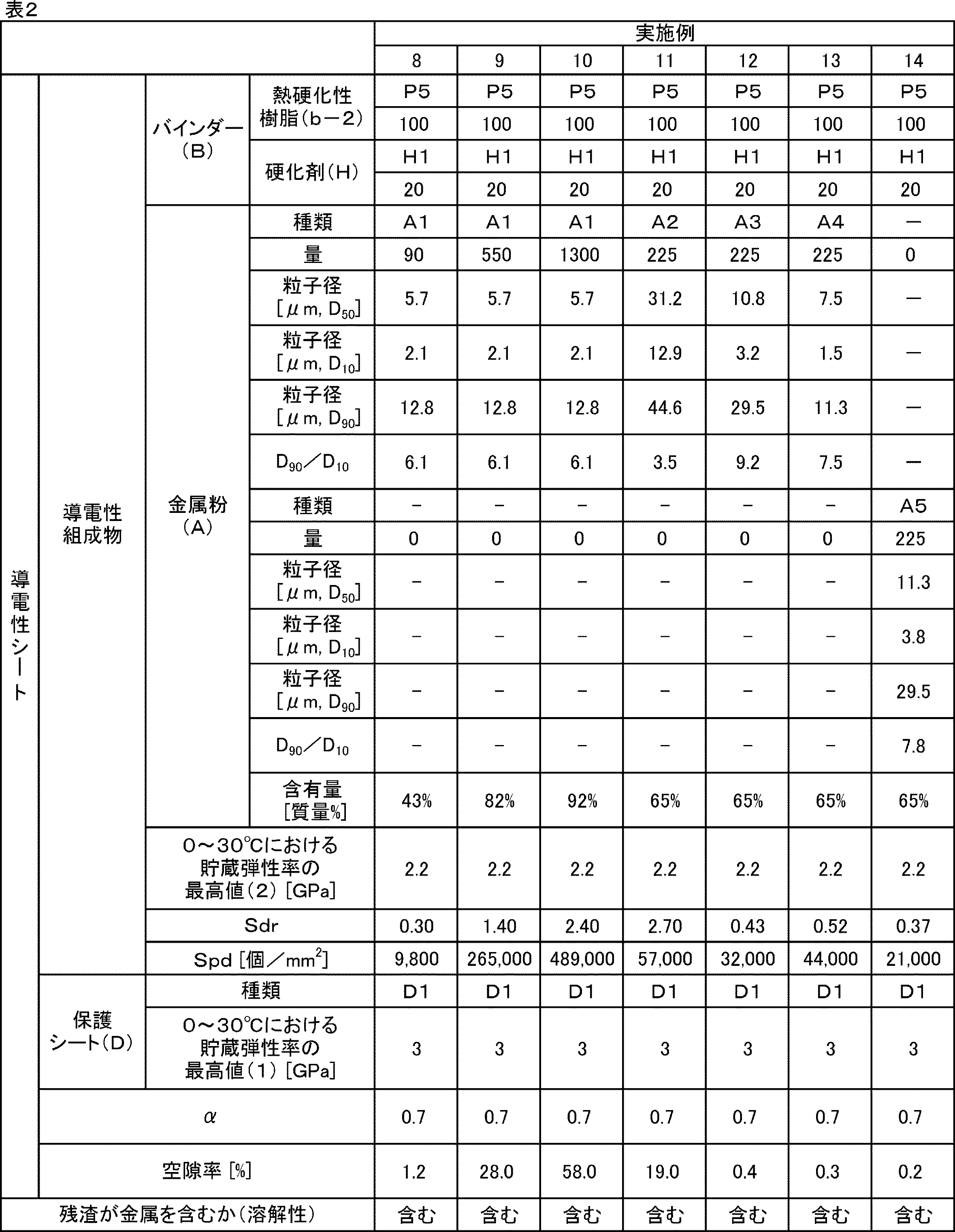
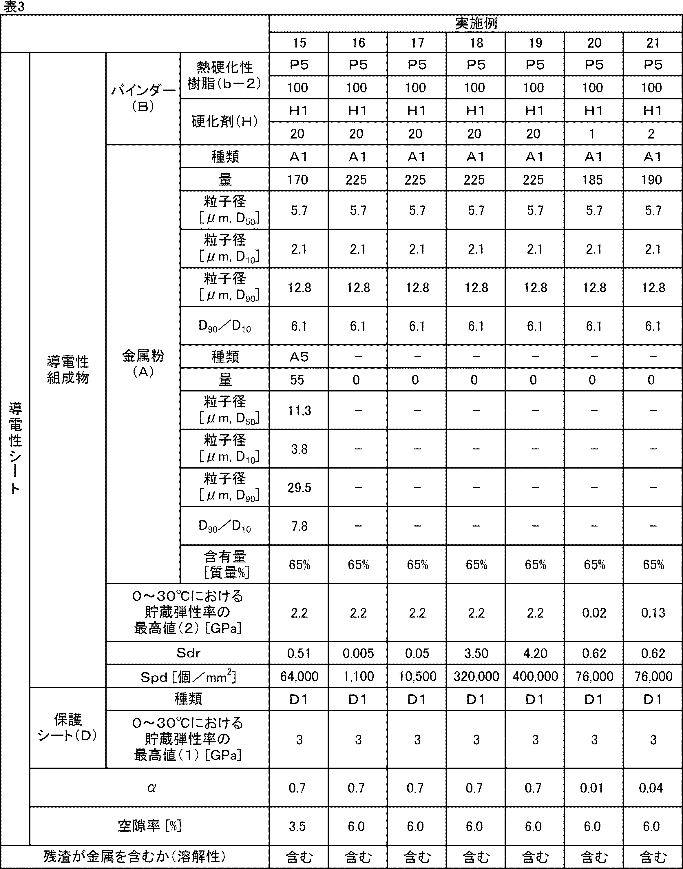
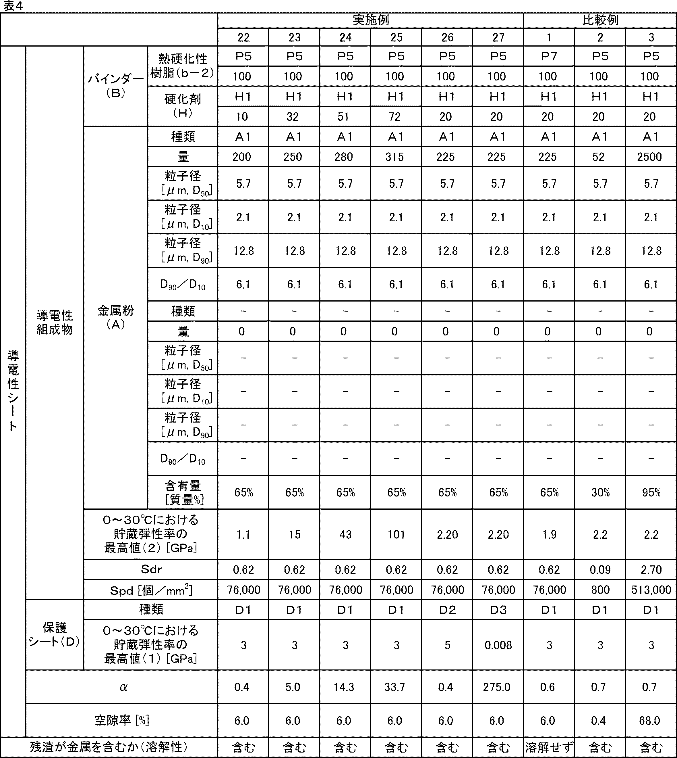
- Examples 2 to 27 and Comparative Examples 1 to 3 Conductive sheets of Examples 2 to 27 and Comparative Examples 1 to 3 were obtained by carrying out the same operation as in Example 1, except that the types and amounts of each component to be blended were as shown in Tables 1 to 4. However, in Examples 16 to 21, Spd and Sdr were adjusted to desired values by buffing the surface of the conductive composition after drying in an electric oven.
- the conductive composition was subdivided compared to the shape before dipping, it was judged as "dissolved”, and it was confirmed whether the insoluble matter (residue) contained metal. If there was no change in the shape from before immersion, it was determined that it did not dissolve. If the change in shape is not visually obvious, compare the mass of the sample before and after immersion, and if the mass loss is less than 5%, it is determined that it is "not dissolved.”
- ⁇ Method for measuring peak density Spd and developed area ratio Sdr> The peak density Spd and developed area ratio Sdr of the protective sheet (D) and the non-opposed surface of the conductive composition (conductive layer) were measured by the following method. After acquiring measurement data on the surface of the conductive composition using a laser microscope (manufactured by Keyence Corporation, VK-X100), the acquired measurement data is analyzed using analysis software (ISO 25178-2:2012 surface texture measurement module " The sample was imported into the analysis application "VK-H1XA” equipped with "VK-H1XR” (both manufactured by Keyence Corporation), and ISO 25178-2:2012 surface texture measurement was performed. The conditions were: S-filter: 1 ⁇ m, L-filter: 0.2 mm.
- ⁇ Measurement of maximum storage modulus of conductive composition (conductive layer) and protective sheet (D) at 0 to 30°C> The maximum value of the storage modulus at 0 to 30°C of each of the conductive composition and the protective sheet (D) was measured by the following method.
- the thickness of the conductive layer was 60 ⁇ m, and the thickness of the protective sheet was the value described in the raw materials.
- Metal recovery is determined by exposing the conductive composition (conductive layer) to a high temperature to carbonize and decompose the binder (B), and then removing the metal component (M1) remaining after carbonizing and decomposing the conductive composition (conductive layer) using a solvent composition ( The evaluation is based on the ratio to the residue (M2) obtained after decomposing the binder (B) by immersion in C).
- the conductive sheets produced in each example and comparative example were cut into pieces with a width of 45 mm and a length of 100 mm, the protective sheet (D) was peeled off, and the resulting conductive composition was heated in an electric furnace at 600°C. After leaving it for 10 hours and taking it out, the mass of the metal component (M1) was measured.
- the conductive sheet was cut into pieces with a width of 45 mm and a length of 100 mm, the protective sheet (D) was peeled off, and the conductive composition obtained was mixed with a solvent composition (C) (nitrogen-containing After being immersed in 100 g of monoethanolamine (20% by mass as an organic solvent (c1), 15% by mass of potassium hydroxide (15% by mass), and 65% by mass of glycerin as a basic inorganic compound (c2)), it was subjected to ultrasonication for 2 hours, The mixture was allowed to stand for 22 hours to allow the residue to settle.
- a solvent composition (C) nitrogen-containing After being immersed in 100 g of monoethanolamine (20% by mass as an organic solvent (c1), 15% by mass of potassium hydroxide (15% by mass), and 65% by mass of glycerin as a basic inorganic compound (c2)
- the conductive sheet prepared in each example and comparative example was cut into a size of 25 mm in width and 100 mm in length, and the surface on which the conductive composition (conductive layer) was exposed was a SUS plate with a width of 30 mm and a length of 150 mm. (A nickel layer with a thickness of 2 ⁇ m was formed on the surface of a commercially available SUS304 plate with a thickness of 0.2 mm.) The conductive sheet was stacked on the SUS plate so as to be in contact with the sheet.
- the conductive sheet and the SUS plate were roll laminated under the conditions of 130°C, 3 kgf/cm 2 and 0.5 m/min, and then the protective sheet (D) was peeled off and the conductive sheet
- a gold-plated copper foil 25 ⁇ m thick copper foil plated with gold
- the conductive composition and gold-plated copper foil were roll laminated to obtain a pre-press laminate. Thereafter, the pre-press laminate was heat-pressed at 150°C and 2MPa, and then left to stand (cured) for 30 minutes in an atmosphere of 180°C to prepare the evaluation sample (SUS plate with conductive adhesive). Obtained.
- Adhesive strength was evaluated according to the following evaluation criteria using adhesive strength as an index. +++: Very good (adhesive strength of 3 N/cm or more). ++: Excellent (adhesive strength is 2 N/cm or more and less than 3 N/cm). +: Practical (adhesive strength is 1 N/cm or more and less than 2 N/cm). NG: Not practical (adhesive strength less than 1 N/cm).
- the conductive sheet (width 20 mm, length 20 mm) prepared in each example and comparative example was used, and the surface on which the conductive composition was exposed was made of a SUS plate (0.1 mm thick) with a width of 20 mm and a length of 20 mm.
- the conductive sheet was placed on the SUS plate so as to be in contact with a commercially available SUS304 plate (with a 2 ⁇ m thick nickel layer formed on the surface).
- the conductive sheet and the SUS board were roll laminated under the conditions of 90° C., 3 kgf/cm 2 and 1 m/min to obtain a conductive sheet-attached SUS board.
- the protective sheet (D) was peeled off from the conductive sheet-attached SUS plate, and then punched into a square with one side of 10 mm using a punching machine. Then, an SUS board with a conductive composition (hereinafter referred to as "SUS board with a conductive composition”) was obtained. Next, the surface of the SUS board with the conductive composition on which the conductive composition was exposed (the surface of the conductive composition not facing the SUS board) was stacked on a separately prepared printed circuit board (flexible printed wiring board), and the conductive composition was placed on a separately prepared printed circuit board (flexible printed wiring board).
- the conductive composition coated SUS board and the flexible printed wiring board were bonded together under the conditions of 130° C., 3 kgf/cm 2 and 1 m/min. Next, these were thermocompression bonded under conditions of 170° C., 2 MPa, and 5 minutes, and then heated at 160° C. for 60 minutes using an electric oven to obtain a sample for evaluation.
- a 32 ⁇ m thick copper foil circuit is formed on each side of a 75 ⁇ m thick polyimide film, and on the copper foil circuit is a square with a side of 0.7 mm and an opening area of 0.7 mm.
- a 37.5 ⁇ m thick adhesive-backed insulating cover film with a 49 mm 2 through hole (opening) is laminated.
- a 37.5 ⁇ m thick insulating cover film with adhesive and no through holes is laminated on the other copper foil circuit (to prevent the printed circuit board from warping, a polyimide film is The copper foil circuit and cover film were arranged symmetrically to the other).
- connection resistance value connection resistance value between the SUS plate of the evaluation sample and the copper foil circuit was measured using a resistance value measuring device and a BSP probe (model number: MCP-TP05P, manufactured by Mitsubishi Chemical Analytech). Using this measured value as an index, conductivity was evaluated according to the following evaluation criteria. +++: Good (connection resistance value less than 20 m ⁇ ). ++: Practical (connection resistance value is 20 m ⁇ or more and less than 100 m ⁇ ). +: Practical (connection resistance value is 100 m ⁇ or more and less than 300 m ⁇ ). NG: Not practical (connection resistance value is 300 m ⁇ or more).
- the conductive sheet produced in each example and comparative example was cut into a size of 25 mm in width and 100 mm in length, and the surface on which the conductive composition was exposed was made of a SUS plate (thickness 0
- the above-mentioned conductive sheet was stacked on the above-mentioned SUS plate so as to be in contact with a 2-mm commercially available SUS304 plate with a 2 ⁇ m-thick nickel layer formed on the surface.
- the conductive sheet and the SUS plate were roll laminated under the conditions of 130° C., 3 kgf/cm 2 and 0.5 m/min to obtain a sample for evaluation.
- the protective sheet (D ) Easy peelability was evaluated according to the following evaluation criteria using the peel strength as an index.
- NG Not practical (peel strength is 400 g/50 mm or more).
- the conductive sheets prepared in each example and comparative example were cut into pieces with a width of 25 mm and a length of 100 mm, left in a freezer (-15°C) for 10 hours, and then taken out in an environment of 23°C and 50% RH. It was left standing for 3 minutes.
- a SUS plate (a nickel layer with a thickness of 2 ⁇ m was formed on the surface of a commercially available SUS304 plate with a thickness of 0.2 mm) has a surface on which the conductive composition (conductive layer) was exposed and had a width of 30 mm and a length of 150 mm.
- the conductive sheet was placed on the SUS plate so as to be in contact with the SUS plate.
- the conductive sheet and the SUS plate were roll laminated under the conditions of 90° C., 3 kgf/cm 2 and 0.5 m/min, and then the protective sheet was peeled off from the conductive sheet, A SUS plate with a conductive layer was obtained.
- the area where the conductive layer of the obtained evaluation sample was present was observed from the electroless gold plating sheet side, and the results were graded from a to d based on the degree of appearance defect (blister due to evaporation of water droplets on the conductive layer).
- Adhesion strength is 6 N/cm or more.
- Adhesive strength is 3 N/cm or more and less than 6 N/cm.
- Adhesive strength is 1 N/cm or more and less than 3 N/cm.
- Adhesive strength is less than 1 N/cm.
- Reworkability was evaluated based on the area of adhesive remaining on the conductive layer when the conductive layer temporarily pasted on polyimide was peeled off, and the arithmetic mean height.
- the exposed surface of the conductive layer of the conductive sheet cut into a width of 50 mm and length of 50 mm was laminated with a polyimide film (Kapton 300H) cut out into a width of 70 mm and length of 70 mm, and then laminated using a roll laminator (conveying speed: 1 m/min, Temperature: 90° C., pressure: 3 kgf/cm 2 ) was passed for temporary pasting.
- the conductive layer in the obtained temporarily pasted laminate was peeled off from the end, and the adhesive residue rate was calculated by dividing the area of the conductive layer remaining on the polyimide by the area of the conductive layer before lamination.
- select five arbitrary points from the remaining adhesive area use a laser microscope (manufactured by Keyence Corporation, VK-X100) to acquire measurement data, and analyze the acquired measurement data using analysis software (ISO 25178 surface texture). It was imported into the analysis application "VK-H1XA" equipped with the measurement module “VK-H1XR” (both manufactured by Keyence Corporation), and the ISO25178 surface texture measurement was performed and the arithmetic mean height was calculated (the conditions were S-filter: 1 ⁇ m, L-filter: 0.2mm).
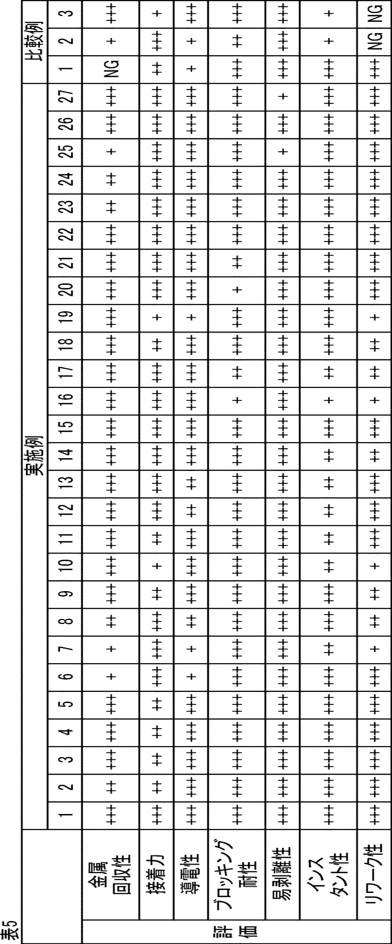
- Comparative Example 1 which did not dissolve in the solvent composition (C), had a problem with metal recovery. Furthermore, Comparative Examples 2 and 3 in which Spd was outside the range of 1000 to 500,000 had problems with reworkability.
- the conductive materials of Examples 1 to 27 which have a conductive layer in which Spd is in the range of 1,000 to 500,000 pieces/mm2, are dissolved in the solvent composition (C), and whose residue contains a metal element It was confirmed that the adhesive sheet had excellent metal recovery properties, adhesive strength, conductivity, blocking resistance, easy peelability, instant property, and reworkability.
Landscapes
- Chemical & Material Sciences (AREA)
- Organic Chemistry (AREA)
- Engineering & Computer Science (AREA)
- Inorganic Chemistry (AREA)
- Physics & Mathematics (AREA)
- Dispersion Chemistry (AREA)
- Spectroscopy & Molecular Physics (AREA)
- Medicinal Chemistry (AREA)
- Chemical Kinetics & Catalysis (AREA)
- Polymers & Plastics (AREA)
- Health & Medical Sciences (AREA)
- Manufacturing & Machinery (AREA)
- Microelectronics & Electronic Packaging (AREA)
- Adhesives Or Adhesive Processes (AREA)
- Conductive Materials (AREA)
- Parts Printed On Printed Circuit Boards (AREA)
- Adhesive Tapes (AREA)
Abstract
Description
例えば特許文献1では、導体回路と補強板とを接合剤層を介して接続することが開示されており、前記接合剤層として、導電粒子と接着剤を含む導電性接着材を用いることが記載されている。また、特許文献2には、熱硬化性樹脂(A)、硬化剤(B)、導電性微粒子(C)、ならびに窒素、リン、および硫黄からなる群から選ばれる少なくともいずれかの元素を含む官能基を有する、シランカップリング剤、シリル化合物、リン酸およびビスフェノールS型エポキシ樹脂からなる群より選択される少なくともいずれかである化合物(D)を含有する導電性接着シートが開示されている。
[1]: 本開示に係る導電性組成物は、保護シート(D)の一主面上に、金属粉(A)とバインダー(B)とを含む導電性組成物が配置されている導電性シートであって、
前記導電性組成物は、30℃の溶剤組成物(C)に24時間浸漬させた場合に、溶解し、且つ残渣が残存するものであって、前記残渣が金属元素を含み、
保護シート(D)と非対向側の前記導電性組成物の表面の山頂点密度Spdが1,000~500,000個/mm2であり、
溶剤組成物(C)は、含窒素有機溶媒(c1)を溶剤組成物(C)の全質量に対し5~40質量%含み、且つ塩基性無機化合物(c2)を溶剤組成物(C)の全質量に対し5~40質量%を含む導電性シート。
[2]: 前記導電性組成物が、接着性を有する、[1]に記載の導電性シート。
[3]: バインダー(B)が、エステル基、イミド基、アミド基、ウレタン基、およびウレア基よりなる群から選択される1種以上を有する、[1]又は[2]記載の導電性シート。
[4]: バインダー(B)が、エステル基、イミド基、アミド基、ウレタン基、およびウレア基よりなる群から選択される2種以上を有する、[1]~[3]のいずれかに記載の導電性シート。
[5]: 保護シート(D)と非対向側の前記導電性組成物の表面の展開面積比Sdrが、0.01~4である[1]~[4]のいずれかに記載の導電性シート。
[6]: 前記導電性組成物の0~30℃における貯蔵弾性率の最高値(2)が0.01~100GPaであり、
前記最高値(2)を保護シート(D)の0~30℃における貯蔵弾性率の最高値(1)で除した値αが0.01~30である、[1]~[5]のいずれか記載の導電性シート。
[7]: 保護シート(D)の0~30℃における貯蔵弾性率の最高値が、0.01~1000GPaである、[1]~[6]のいずれかに記載の導電性シート。
[8]: 金属板、[1]~[7]のいずれかいずれか1項記載の導電性シートの保護シート(D)を剥離して得た導電性組成物および配線回路基板を含み、
前記導電性組成物を介して前記配線回路基板に前記金属板が固定されている配線板。
[9]: [8]記載の配線板を具備する電子機器。
[10]: 金属粉(A)とバインダー(B)とを含む導電性組成物であって、含窒素有機溶媒(c1)を5~40質量%、塩基性無機化合物(c2)を5~40質量%、含む溶剤組成物(C)に30℃、24時間浸漬させた際、一部が溶解し、一部が不溶であって、不溶分中に金属粉(A)に由来する金属元素を含む、導電性組成物。
[11]: 接着性を有する、[10]記載の導電性組成物。
[12]: バインダー(B)が、エステル基、イミド基、アミド基、ウレタン基、及びウレア基よりなる群から選択される1種以上を有する、[10]又は[11]記載の導電性組成物。
[13]: バインダー(B)が、エステル基、イミド基、アミド基、ウレタン基、及びウレア基よりなる群から選択される2種以上を有する、[10]~[12]のいずれかに記載の導電性組成物。
本開示の導電性組成物は、金属粉(A)およびバインダー(B)を含む。この導電性組成物を、含窒素有機溶媒(c1)を5~40質量%、および塩基性無機化合物(c2)を5~40質量%含む溶剤組成物(C)に30℃、24時間浸漬させた際、一部が溶解し、一部が不溶であって、不溶分中に金属粉(A)に由来する金属元素を含む。換言すると、本導電性組成物が溶解し、且つ残渣が残る。この残渣には金属粉(A)に由来する金属元素が含まれる。
金属粉(A)は、導電性組成物に導電性を付与する目的で用いられる。
金属粉(A)は、金、白金、銀、銅およびニッケル等の導電性金属、およびその合金が好ましい。単一組成の微粒子に代えて、核体と、前記核体よりも導電性が高い素材で形成した、前記核体表面を被覆する被覆層を有する複合微粒子を用いてもよい。複合微粒子はコストダウンの観点から好ましい。前記核体は、導電性の金属およびその合金が好ましく、その中でもニッケル、シリカ、銅から選択することがより好ましい。前記被覆層は、導電性を有する素材であればよく、導電性金属または導電性ポリマーが好ましい。導電性金属は、例えば、金、白金、銀、錫、マンガンおよびインジウム、ならびにその合金が挙げられる。これらの中でも導電性の点から銀が好ましい。
バインダー(B)は、導電性組成物の基体となり金属粉(A)を分散担持する機能を有する。バインダー(B)は、溶剤組成物(C)によって分解される必要があることから、有機物が好ましい。バインダー(B)は前述した機能を有するものであれば、特に組成等は制限されないが、樹脂(b-1)を含むことが好ましい。本開示における樹脂(b-1)は、常温で固体、半固体、又は凝固体であり、軟化又は溶融範囲を有する、重量平均分子量(Mw)が5,000以上の有機材料と定義される。
樹脂(b-1)は、前述した重量平均分子量(Mw)以外には特に組成、分子構造等は制限されないが、イミド結合、アミド結合、ウレタン結合およびウレア結合よりなる群から選択される1種以上の化学結合を有する樹脂が好ましい。
更に、金属粉(A)を分散担持する機能を発現する観点から、樹脂(b-1)は、熱硬化性樹脂、熱可塑性樹脂、紫外線硬化樹脂等の光硬化性樹脂、天然樹脂、エラストマーであることが好ましく、導電性組成物に優れた接着性を付与する観点からは、樹脂(b-1)は熱硬化性樹脂(b-2)であることが好ましい。
熱硬化性樹脂(b-2)は、樹脂(b-1)のうち、熱硬化性を有するものである。熱硬化性とは「熱によって、重合および/又は架橋反応を生じ、不可逆的に弾性率が上昇すること」と定義される。
硬化剤(H)は前記熱硬化性樹脂(b)との組み合わせにより硬化性を発揮する公知の化合物の中から適宜選択すればよい。硬化剤(H)としては、例えば、エポキシ化合物、オキセタン化合物、エピスルフィド化合物、アジリジン化合物、イソシアネート化合物、アミン化合物、イソシアネート化合物、イミダゾール化合物および酸無水物が挙げられる。
硬化剤(H)の含有量が1質量部以上であることで、導電性組成物をBステージ硬化状態とすることができる。Bステージ硬化とは、導電性組成物を所定の温度、時間で加熱することにより、含有する硬化剤(H)の硬化反応を部分的に生じさせる方法である。Bステージ硬化を行うことにより、導電性組成物の接着力を維持しつつ、強度を高めることができるとともに、導電性組成物の弾性を高めることでブロッキング耐性を向上させることができる。また、硬化剤(H)の含有量が70質量部以下であることで、導電性組成物を硬化させた際に過剰な架橋構造の形成を抑制し、溶剤組成物(C)へのバインダー(B)の溶解性を高めることができる。
本開示の溶剤組成物(C)は、含窒素有機溶媒(c1)および塩基性無機化合物(c2)を含む。溶剤組成物(C)の溶解性効果をバインダー(B)に効率的に作用させる観点から、溶剤組成物(C)は含窒素有機溶媒(c1)を溶剤組成物(C)の全質量に対し5~40質量%含む。含窒素有機溶媒(c1)の含有量は、10~30質量%であることがより好ましい。含窒素有機溶媒(c1)は、分子中に窒素原子を含む有機溶媒であれば特に制限なく使用できる。具体的には、N-メチル-2-ピロリドン、ノルマルプロピルブロマイド、γ-ブチロラクトン、モノエタノールアミン、ジエタノールアミンおよびトリエタノールアミン等を用いることができ、溶解させるバインダー(B)の含有物によって適宜種類を選択できる。
本実施の形態にかかる導電性シートは、保護シート(D)の一主面(一方の面のみ)に金属粉(A)とバインダー(B)とを含む導電性組成物が配置されている導電性シートである。換言すると、本導電性シートは保護シート(D)上に導電性組成物を有するシート状物品である。なお、導電性シートに具備される導電性組成物は、室温で非流動性の固形物であり、且つ一定の厚みの層状を成しており導電層ともいう。この導電層は、30℃の溶剤組成物(C)に24時間浸漬させた場合に、溶解し、且つ残渣が残存するものであって、前記残渣が金属元素を含む。
保護シート(D)は、片面あるいは両面に離型処理をしたフィルムであれば、適宜使用できる。
保護シート(D)の基材の一例としては、ポリエチレンテレフタレート、ポリエチレンナフタレート、ポリフッ化ビニル、ポリフッ化ビニリデン、硬質ポリ塩化ビニル、ポリ塩化ビニリデン、ナイロン、ポリイミド、ポリスチレン、ポリビニルアルコール、エチレン・ビニルアルコール共重合体、ポリカーボネート、ポリアクリロニトリル、ポリブテン、軟質ポリ塩化ビニル、ポリフッ化ビニリデン、ポリエチレン、ポリプロピレン、ポリウレタン、エチレン酢酸ビニル共重合体、ポリ酢酸ビニル等のプラスチックシート;グラシン紙、上質紙、クラフト紙、コート紙等の紙類;各種の不織布、合成紙、金属箔や、これらを組み合わせた複合フィルムが挙げられる。これらの中でもポリエチレンテレフタレートおよびポリエチレンナフタレートが易剥離性を高める観点から好ましい。
本開示の導電性シートは、保護シート(D)と対向していない(非対向側の)導電性組成物(導電層)の表面の山頂点密度Spdが1,000~500,000個/mm2である。当該面の山頂点密度Spdがこの範囲であることで、被着体との接点を適度な範囲とし、被着体への過度な密着を抑制することで、リワーク性を向上させることができる。山頂点密度Spdは、10,000~300,000個/mm2であることが好ましく、25,000~250,000個/mm2であることが更に好ましい。
本開示の導電性シート表面の山頂点密度Spd、展開面積比Sdrを制御する方法は、物体の表面形状を調整する方法として従来公知の方法を適用できる。SpdとSdrそれぞれ異なった方法を適用しても、共通した方法を適用してもよい。例えば、研磨布紙を用いて表面を研磨する方法、圧縮空気によって研磨材を導電性組成物表面に吹き付けるショットブラスト法、所定の山頂点密度Spd、展開面積比Sdrを有するフィルムの上に導電性組成物を形成し、保護シートを積層した後にフィルムを除去し、フィルム表面の凹凸を転写する方法、所定の山頂点密度Spd、展開面積比Sdrを有するフィルムと導電性組成物を圧着し、フィルム表面の凹凸を転写する方法、導電性組成物に粒子状物質を含有させて表面凹凸を制御する方法が挙げられる。
本開示の導電性シートは、例えば、導電性組成物を保護シート(D)上に塗工し、乾燥し、更に必要に応じてBステージ硬化することで得ることができる。塗工方法は、公知の方法の中から、接合剤の膜厚等を考慮して適宜選択すればよい。塗工方法の具体例としては、グラビアコート方式、キスコート方式、ダイコート方式、リップコート方式、コンマコート方式、ブレードコート方式、ロールコート方式、ナイフコート方式、スプレーコート方式、バーコート方式、スピンコート方式、ディップコート方式が挙げられる。
本配線板の製造方法は、一例として、プリント配線板用の配線回路基板と、導電性組成物と、金属板とを積層し、これを圧着して接合し、次いで基板上に電子部品を実装する方法が挙げられる。以下に配線板の製造方法の一例を説明する。
本配線板は、プリント配線板が用いられる従来公知のあらゆる製品に適用できる。具体的には、携帯電話、スマートフォン、ノートPC、デジタルカメラ、液晶ディスプレイ等の電子機器に適用できる。自動車、電車、船舶、航空機等の輸送機器に好適に用いることができる。
D50平均粒子径は、レーザー回折・散乱法粒度分布測定装置LS13320(ベックマン・コールター社製)により測定した。トルネードドライパウダーサンプルモジュールにて、導電性フィラーを測定して得た数値であり、粒子径累積分布における累積値が50%の粒子径である。なお、屈折率の設定は1.6とした。D10、D90は、粒子径累積分布における累積値が10%、90%の粒子径平均粒子径であり、上記と同様に測定した。
JIS K 0070の中和滴定法に準拠し、測定した酸価(mgKOH/g)を固形分換算することで求めた。共栓三角フラスコ中に試料約1gを精密に量り採り、テトラヒドロフラン/エタノール(容量比:テトラヒドロフラン/エタノール=2/1)混合液100mLを加えて溶解する。これに、フェノールフタレイン試液を指示薬として加え、0.1Nアルコール性水酸化カリウム溶液で滴定し、指示薬が淡紅色を30秒間保持した時を終点とした。酸価は次式により求めた(単位:mgKOH/g)。
酸価(mgKOH/g)=(5.611×a×F)/S
ただし、
S:試料の採取量(g)
a:0.1Nアルコール性水酸化カリウム溶液の消費量(mL)
F:0.1Nアルコール性水酸化カリウム溶液の力価
Mwの測定はGPC(ゲルパーミエーションクロマトグラフ)「HPC-8020」(東ソー社製)により行った。GPCは溶媒(THF:テトラヒドロフラン)に溶解した物質をその分子サイズの差によって分離定量する液体クロマトグラフである。本測定は、カラムに「LF-604」(昭和電工社製:迅速分析用GPCカラム:6mmID×150mmサイズ)を直列に2本接続して用い、流量0.6mL/min、カラム温度40℃の条件で行った。Mwの決定はポリスチレン換算で行った。
各導電性組成物の作製に用いる原料を以下に示す。
金属粉(A)
A1:銀被覆銅粉:D50=5.7μm、D10=2.1μm、D90=12.8μm、樹枝状(三井金属鉱業製)
A2:銀被覆銅粉:D50=31.2μm、D10=12.9μm、D90=44.6μm、樹枝状(三井金属鉱業製)
A3:銀被覆銅粉:D50=10.8μm、D10=3.2μm、D90=29.5μm、球状(昭和電工マテリアル製)
A4:銀被覆銅粉:D50=7.5μm、D10=1.5μm、D90=11.3μm、球状(昭和電工マテリアル製)
A5:銀被覆銅粉:D50=11.3μm、D10=3.8μm、D90=29.5μm、フレーク状(DOWAホールディングス製)
バインダー(B)
熱硬化性樹脂(b-2)
P1:ポリエステル樹脂(エステル基を有する熱硬化性樹脂):酸価36mgKOH/g、Mw=27,000(トーヨーケム製)
P2:ポリイミド樹脂(イミド基を有する熱硬化性樹脂):酸価=22mgKOH/g、Mw=55,000(トーヨーケム製)
P3:ポリアミド樹脂(アミド基を有する熱硬化性樹脂):酸価=28mgKOH/g、Mw=49,000(トーヨーケム製)
P4:ポリマレイミド樹脂(イミド基を有する熱硬化性樹脂):酸価=13mgKOH/g、Mw=98,000(トーヨーケム製)
P5:ポリウレタンイミド樹脂(ウレタン基とイミド基を有する熱硬化性樹脂):酸価=11mgKOH/g、Mw=100,000(トーヨーケム製)
P6:ポリアクリル樹脂(エステル基、イミド基、アミド基、ウレタン基およびウレア基のいずれも有さない熱硬化性樹脂):酸価=17mgKOH/g、Mw=120,000(トーヨーケム製)
P7:ポリオレフィン樹脂(エステル基、イミド基、アミド基、ウレタン基およびウレア基のいずれも有さない熱硬化性樹脂):酸価=26mgKOH/g、Mw=85,000(トーヨーケム製)
硬化剤(H)
H1:ビスフェノールA型エポキシ化合物(jER834、分子量=470、三菱ケミカル製)
保護シート(D)
D1:50μmのPET(ポリエチレンテレフタレート)フィルムにサンドブラスト法によってマット化処理を施し、シリコーン剥離剤を塗布した保護シート
D2:50μmのPEN(ポリエチレンナフタレート)フィルムにサンドブラスト法によってマット化処理を施し、シリコーン剥離剤を塗布した保護シート
D3:38μmのPP(ポリプロピレン)フィルムにサンドブラスト法によってマット化処理を施し、シリコーン剥離剤を塗布した保護シート
[実施例1]
熱硬化性樹脂(b-2)としてポリウレタンイミド樹脂(P5)を100質量部、金属粉(A)として樹枝状金属粉(A1)225質量部を容器に仕込み、硬化剤(H)としてエポキシ化合物(H1)20質量部を加え、不揮発分濃度が45質量%となるようにMEKを加えて混合した。攪拌機により10分間攪拌して導電性組成物ワニスを調製した。
配合する各成分の種類および配合量を表1~4に記載した通りとした以外は実施例1と同様に操作し、実施例2~27および比較例1~3の導電性シートを得た。ただし、実施例16~21については、電気オーブンでの乾燥後に導電性組成物の表面をバフ研磨することによりSpd、Sdrを所望の値に調整した。
導電性組成物(導電層)が溶剤組成物(C)に溶解し、且つ残渣が金属を含むか(溶解性)について、以下の方法により確認した。導電性シートを、幅45mm、長さ100mmの大きさに切断し、保護シート(D)を剥がして得られた導電性組成物を、30℃の溶剤組成物(C)(含窒素有機溶媒(c1)としてモノエタノールアミン:20質量%、塩基性無機化合物(c2)として水酸化カリウム:15質量%、グリセリン:65質量%を含む)100gに浸漬した後に2時間超音波処理し、22時間静置し、導電性組成物が浸漬前の形状と比較して細分化されている場合は「溶解した」と判断し、不溶分(残渣)が金属を含むか否かの確認を行った。浸漬前の形状と変化が無い場合は「溶解せず」と判定した。なお、形状変化が目視で明らかでない場合には、試料の浸漬前後の質量を比較し、質量減損が5%未満である場合を「溶解せず」と判定する。
導電性組成物(導電層)の保護シート(D)と非対向面の山頂点密度Spd、展開面積比Sdrは、以下の方法により測定した。導電性組成物の表面をレーザーマイクロスコープ(キーエンス社製、VK-X100)を使用し、測定データ取得を行った後、取得した測定データを解析ソフトウェア(ISO 25178-2:2012表面性状計測モジュール「VK-H1XR」を備えた、解析アプリケーション「VK-H1XA」、ともにキーエンス社製)に取り込み、ISO 25178-2:2012表面性状計測を実行した。条件は、S‐フィルター:1μm、L‐フィルター:0.2mmとした。
導電性組成物および保護シート(D)のそれぞれの0~30℃における貯蔵弾性率の最高値は、以下の方法により測定した。導電層の厚みは60μm、保護シートの厚みは原料に記載した値とした。
まず、幅5mm・長さ30mmの測定用試料を用意し、この試料を動的粘弾性測定装置(動的粘弾性測定装置DVA-200、アイティー計測制御社製)にセットし、昇温速度:10℃/分、測定周波数:1Hz、歪:0.08%の条件にて動的粘弾性測定を行い、得られた動的粘弾性曲線より、0~30℃における貯蔵弾性率E’を読取り、最高値を求めた。
得られた各導電性組成物について、金属回収性、接着力、導電性、ブロッキング耐性、易剥離性、インスタント性およびリワーク性を下記方法に従って評価した。評価結果を表5に示す。
金属回収性は、導電性組成物(導電層)を高温曝露させてバインダー(B)を炭化、分解させた後に残る金属成分(M1)と、導電性組成物(導電層)を溶剤組成物(C)に浸漬してバインダー(B)を分解させた後に得られる残渣(M2)との比によって評価する。
各実施例および比較例にて作製した導電性シートを、幅45mm、長さ100mmの大きさに切断し、保護シート(D)を剥がして得られた導電性組成物を、600℃の電気炉に10時間静置し、取り出した後に金属成分(M1)の質量を測定した。
また、同じく導電性シートを、幅45mm、長さ100mmの大きさに切断し、保護シート(D)を剥がして得られた導電性組成物を、30℃の溶剤組成物(C)(含窒素有機溶媒(c1)としてモノエタノールアミン:20質量%、塩基性無機化合物(c2)として水酸化カリウム:15質量%、グリセリン:65質量%を含む)100gに浸漬した後に2時間超音波処理し、22時間静置し、残渣を沈降させた。その後、上澄みの溶剤組成物(C-1)をイソプロパノールに置換し、再度5時間静置した後に、上澄み液を除去し、3日間風乾した後に得られた残渣(M2)の質量を測定した。M1をM2で除した値を求め、下記基準に従い、金属回収性を評価した。
+++:非常に優れている(M1/M2が0.95以上)。
++:優れている(M1/M2が0.80以上、0.95未満)。
+:実用可能である(M1/M2が0.50以上、0.80未満)。
NG:実用不可能である(M1/M2が0.50未満)。
各実施例および比較例にて作製した導電性シートを幅25mm、長さ100mmの大きさに切断し、その導電性組成物(導電層)が露出した面が幅30mm、長さ150mmのSUS板(厚さ0.2mmの市販のSUS304板の表面に厚さ2μmのニッケル層を形成したもの)に接触するように、上記導電性シートを上記SUS板に重ねた。次いで、ロールラミネーターを用い、130℃、3kgf/cm2、0.5m/minの条件下で、上記導電性シートと上記SUS板とをロールラミネートした後、保護シート(D)を剥がし、導電性組成物が露出面に金めっき銅箔(厚さ25μmの銅箔を金めっき処理したもの)を重ね、ロールラミネーターを用い、130℃、3kgf/cm2、0.5m/minの条件下で、導電性組成物と金めっき銅箔をロールラミネートし、プレス前積層物を得た。その後、プレス前積層物を150℃、2MPaの条件で加熱プレスを行った後、180℃雰囲気下で30分静置(キュア)させることにより、評価用試料(導電性接着剤付SUS板)を得た。
+++:非常に優れている(接着強度が3N/cm以上)。
++:優れている(接着強度が2N/cm以上3N/cm未満)。
+:実用可能である(接着強度が1N/cm以上2N/cm未満)。
NG:実用不可能である(接着強度が1N/cm未満)。
各実施例および比較例にて作製した導電性シート(幅20mm、長さ20mm)を用い、その導電性組成物が露出した面が幅20mm、長さ20mmのSUS板(厚さ0.1mmの市販のSUS304板の表面に厚さ2μmのニッケル層を形成したもの)に接触するように、上記導電性シートを上記SUS板に重ねた。次いで、ロールラミネーターを用い、90℃、3kgf/cm2、1m/minの条件下で、上記導電性シートと上記SUS板とをロールラミネートして導電性シート付SUS板を得た。
+++:良好である(接続抵抗値が20mΩ未満)。
++:実用可能である(接続抵抗値が20mΩ以上100mΩ未満)。
+:実用可能である(接続抵抗値が100mΩ以上300mΩ未満)。
NG:実用不可能である(接続抵抗値が300mΩ以上)。
各実施例および比較例にて作製した導電性シート(幅50mm、長さ50mm)をそれぞれ2枚準備した。そして、導電性シートの導電性組成物が露出した面と、もう一方の導電性シートの保護シート(D)が露出した面(即ち、剥離性剤が塗布されていない面)が接触するようにそれぞれの導電性シートを重ね合わせ、2kgの重りを載せた後に、40℃、大気圧の条件下で3日間静置した。その後、重りを除去し、それぞれの導電性シートを引き離した際に、保護シート(D)に導電性組成物が転写された面積を指標として、下記評価基準に従いブロッキング耐性を評価した。
+++:良好である(転写した面積が5%未満)。
++:実用可能である(転写した面積が5%以上10%未満)。
+:実用可能である(転写した面積が10%以上20%未満)。
NG:実用不可能である(転写した面積が20%以上)。
各実施例および比較例にて作製した導電性シートを幅25mm、長さ100mmの大きさに切断し、その導電性組成物が露出した面が幅30mm、長さ150mmのSUS板(厚さ0.2mmの市販のSUS304板の表面に厚さ2μmのニッケル層を形成したもの)に接触するように、上記導電性シートを上記SUS板に重ねた。次いで、ロールラミネーターを用い、130℃、3kgf/cm2、0.5m/minの条件下で、上記導電性シートと上記SUS板とをロールラミネートし、評価用試料を得た。
+++:非常に優れている(剥離強度が50g/50mm未満)。
++:優れている(剥離強度が50g/50mm以上100g/50mm未満)。
+:実用可能である(剥離強度が100g/50mm以上400g/50mm未満)。
NG:実用不可能である(剥離強度が400g/50mm以上)。
各実施例および比較例にて作製した導電性シートを幅25mm、長さ100mmの大きさに切断し、冷凍庫(-15℃)に10時間静置し、その後取り出して23℃50%RHの環境に3分間静置した。次いで、その導電性組成物(導電層)が露出した面が幅30mm、長さ150mmのSUS板(厚さ0.2mmの市販のSUS304板の表面に厚さ2μmのニッケル層を形成したもの)に接触するように、上記導電性シートを上記SUS板に重ねた。次いで、ロールラミネーターを用い、90℃、3kgf/cm2、0.5m/minの条件下で、上記導電性シートと上記SUS板とをロールラミネートした後、上記導電性シートから保護シートを剥がし、導電層付SUS板を得た。
a:導電層の面積に対し、膨れの面積が5%以上、10%未満。
b:導電層の面積に対し、膨れの面積が10%以上、15%未満。
c:導電層の面積に対し、膨れの面積が15%以上、20%未満。
d:導電層の面積に対し、膨れの面積が5%未満。
a:接着強度が6N/cm以上。
b:接着強度が3N/cm以上6N/cm未満。
c:接着強度が1N/cm以上3N/cm未満。
d:接着強度が1N/cm未満。
+++:膨れ評価、接着強度ともにa(非常に優れている)
++:膨れ評価、接着強度のどちらか一方がa且つもう一方がb、もしくは両方がb(優れている)
+:膨れ評価、接着強度のどちらかがcでdがない(実用可能である)
NG:膨れ評価、接着強度のどちらかまたは両方がd(実用不可能である)
リワーク性は、ポリイミドに仮貼りした導電層を剥がした際の導電層の糊残り面積と算術平均高さで評価した。幅50mm・長さ50mmに切出した導電性シートの導電層が露出した面を、幅70mm・長さ70mmに切出したポリイミドフィルム(カプトン300H)と貼り合せ、ロールラミネーター(搬送速度:1m/分、温度:90℃、圧力:3kgf/cm2)を通過させて仮貼りを行った。得られた仮貼り積層体中の導電層を端部から剥がし、ポリイミド上に残った導電層の面積を、貼り合せ前の導電層の面積で除することにより糊残り率を算出した。次いで、糊残り部分から任意の5点を選択し、表面をレーザーマイクロスコープ(キーエンス社製、VK-X100)を使用し、測定データ取得を行い、取得した測定データを解析ソフトウェア(ISO 25178表面性状計測モジュール「VK-H1XR」を備えた、解析アプリケーション「VK-H1XA」、ともにキーエンス社製)に取り込み、ISO25178表面性状計測を実行し、算術平均高さを算出した(条件は、S‐フィルター:1μm、L‐フィルター:0.2mm)。これによって得られた糊残り率、算術平均高さを用いて、下記の基準で評価した。
+++:糊残り率が5%以下、且つ糊残りした部分がある場合には、その算術平均高さが接着剤層厚さの20%未満である。極めて良好である。
++:糊残り率が5%越え、15%以下であり、且つその算術平均高さが接着剤層厚さの20%未満である。良好である。
+:糊残り率が15%以下、且つ糊残りした部分の算術平均高さが接着剤層厚さの20~50%。実用可。
NG:糊残り率が15%より大きい、および/又は糊残りした部分の算術平均高さが接着剤層厚さの50%より大きい。実用不可。

Claims (9)
- 保護シート(D)の一主面上に、金属粉(A)とバインダー(B)とを含む導電性組成物が配置されている導電性シートであって、
前記導電性組成物は、30℃の溶剤組成物(C)に24時間浸漬させた場合に、溶解し、且つ残渣が残存するものであって、前記残渣が金属元素を含み、
保護シート(D)と非対向側の前記導電性組成物の表面の山頂点密度Spdが1,000~500,000個/mm2であり、
溶剤組成物(C)は、含窒素有機溶媒(c1)を溶剤組成物(C)の全質量に対し5~40質量%含み、且つ塩基性無機化合物(c2)を溶剤組成物(C)の全質量に対し5~40質量%含む導電性シート。 - 前記導電性組成物が、接着性を有する、請求項1に記載の導電性シート。
- バインダー(B)が、エステル基、イミド基、アミド基、ウレタン基、およびウレア基よりなる群から選択される1種以上を有する、請求項1記載の導電性シート。
- バインダー(B)が、エステル基、イミド基、アミド基、ウレタン基、およびウレア基よりなる群から選択される2種以上を有する、請求項1に記載の導電性シート。
- 保護シート(D)と非対向側の前記導電性組成物の表面の展開面積比Sdrが、0.01~4である請求項1に記載の導電性シート。
- 前記導電性組成物の0~30℃における貯蔵弾性率の最高値(2)が0.01~100GPaであり、
前記最高値(2)を保護シート(D)の0~30℃における貯蔵弾性率の最高値(1)で除した値αが0.01~30である、請求項1記載の導電性シート。 - 保護シート(D)の0~30℃における貯蔵弾性率の最高値が、0.01~1000GPaである、請求項1に記載の導電性シート。
- 金属板、請求項1~7いずれか1項記載の導電性シートの保護シート(D)を剥離して得た導電性組成物および配線回路基板を含み、
前記導電性組成物を介して前記配線回路基板に前記金属板が固定されている配線板。 - 請求項8記載の配線板を具備する電子機器。
Priority Applications (5)
| Application Number | Priority Date | Filing Date | Title |
|---|---|---|---|
| KR1020237042978A KR102906310B1 (ko) | 2022-04-22 | 2023-04-19 | 도전성 시트, 배선판 및 전자 기기 |
| KR1020257043276A KR20260010518A (ko) | 2022-04-22 | 2023-04-19 | 도전성 시트, 배선판 및 전자 기기 |
| JP2023566732A JP7697530B2 (ja) | 2022-04-22 | 2023-04-19 | 導電性シート、配線板および電子機器 |
| CN202380012520.1A CN117616095A (zh) | 2022-04-22 | 2023-04-19 | 导电性片、接线板和电子设备 |
| JP2025097137A JP2025124896A (ja) | 2022-04-22 | 2025-06-10 | 導電性シート、配線板および電子機器 |
Applications Claiming Priority (2)
| Application Number | Priority Date | Filing Date | Title |
|---|---|---|---|
| JP2022-070493 | 2022-04-22 | ||
| JP2022070493 | 2022-04-22 |
Publications (1)
| Publication Number | Publication Date |
|---|---|
| WO2023204253A1 true WO2023204253A1 (ja) | 2023-10-26 |
Family
ID=88419926
Family Applications (1)
| Application Number | Title | Priority Date | Filing Date |
|---|---|---|---|
| PCT/JP2023/015645 Ceased WO2023204253A1 (ja) | 2022-04-22 | 2023-04-19 | 導電性シート、配線板および電子機器 |
Country Status (5)
| Country | Link |
|---|---|
| JP (2) | JP7697530B2 (ja) |
| KR (2) | KR102906310B1 (ja) |
| CN (1) | CN117616095A (ja) |
| TW (1) | TW202342673A (ja) |
| WO (1) | WO2023204253A1 (ja) |
Citations (4)
| Publication number | Priority date | Publication date | Assignee | Title |
|---|---|---|---|---|
| JPH08217955A (ja) * | 1995-02-17 | 1996-08-27 | Matsushita Electric Ind Co Ltd | 導電性組成物 |
| JP2015185717A (ja) * | 2014-03-25 | 2015-10-22 | 東洋インキScホールディングス株式会社 | 導電性接着シート、電磁波シールドシートおよびプリント配線板 |
| CN109943252A (zh) * | 2019-02-28 | 2019-06-28 | 苏州金枪新材料股份有限公司 | 一种银包铜导电胶及其制备方法 |
| WO2020122114A1 (ja) * | 2018-12-12 | 2020-06-18 | 大塚化学株式会社 | 透明導電層形成用基材、透明導電性フィルム、タッチパネルおよび透明導電層形成用基材の製造方法 |
Family Cites Families (8)
| Publication number | Priority date | Publication date | Assignee | Title |
|---|---|---|---|---|
| JP4319298B2 (ja) * | 1998-10-02 | 2009-08-26 | 三井化学ポリウレタン株式会社 | ポリウレタン樹脂の分解回収方法 |
| JP4843979B2 (ja) | 2004-03-30 | 2011-12-21 | 住友ベークライト株式会社 | 回路基板 |
| JP5678773B2 (ja) * | 2011-03-31 | 2015-03-04 | 東洋インキScホールディングス株式会社 | 導電性樹脂組成物および導電性接着シ−ト |
| JP2013075950A (ja) * | 2011-09-29 | 2013-04-25 | Kaneko Kagaku:Kk | 合成樹脂溶解用溶剤組成物 |
| US20140281980A1 (en) | 2013-03-15 | 2014-09-18 | Chad A. Hage | Methods and Apparatus to Identify a Type of Media Presented by a Media Player |
| JP2015109404A (ja) * | 2013-10-24 | 2015-06-11 | 信越ポリマー株式会社 | 電磁波シールドフィルム、電磁波シールドフィルム付きフレキシブルプリント配線板、およびそれらの製造方法 |
| JP6694763B2 (ja) * | 2016-06-08 | 2020-05-20 | 信越ポリマー株式会社 | 電磁波シールドフィルムおよび電磁波シールドフィルム付きプリント配線板 |
| JP7107344B2 (ja) * | 2020-10-06 | 2022-07-27 | 東洋インキScホールディングス株式会社 | 金属板用接合剤、プリント配線板用補強部材及びその製造方法、並びに、配線板及びその製造方法 |
-
2023
- 2023-04-19 KR KR1020237042978A patent/KR102906310B1/ko active Active
- 2023-04-19 WO PCT/JP2023/015645 patent/WO2023204253A1/ja not_active Ceased
- 2023-04-19 CN CN202380012520.1A patent/CN117616095A/zh active Pending
- 2023-04-19 KR KR1020257043276A patent/KR20260010518A/ko active Pending
- 2023-04-19 JP JP2023566732A patent/JP7697530B2/ja active Active
- 2023-04-21 TW TW112114999A patent/TW202342673A/zh unknown
-
2025
- 2025-06-10 JP JP2025097137A patent/JP2025124896A/ja active Pending
Patent Citations (4)
| Publication number | Priority date | Publication date | Assignee | Title |
|---|---|---|---|---|
| JPH08217955A (ja) * | 1995-02-17 | 1996-08-27 | Matsushita Electric Ind Co Ltd | 導電性組成物 |
| JP2015185717A (ja) * | 2014-03-25 | 2015-10-22 | 東洋インキScホールディングス株式会社 | 導電性接着シート、電磁波シールドシートおよびプリント配線板 |
| WO2020122114A1 (ja) * | 2018-12-12 | 2020-06-18 | 大塚化学株式会社 | 透明導電層形成用基材、透明導電性フィルム、タッチパネルおよび透明導電層形成用基材の製造方法 |
| CN109943252A (zh) * | 2019-02-28 | 2019-06-28 | 苏州金枪新材料股份有限公司 | 一种银包铜导电胶及其制备方法 |
Also Published As
| Publication number | Publication date |
|---|---|
| JP2025124896A (ja) | 2025-08-26 |
| CN117616095A (zh) | 2024-02-27 |
| KR20240007266A (ko) | 2024-01-16 |
| TW202342673A (zh) | 2023-11-01 |
| JP7697530B2 (ja) | 2025-06-24 |
| KR102906310B1 (ko) | 2025-12-31 |
| JPWO2023204253A1 (ja) | 2023-10-26 |
| KR20260010518A (ko) | 2026-01-20 |
Similar Documents
| Publication | Publication Date | Title |
|---|---|---|
| TWI703199B (zh) | 導電性接著劑層、導電性接著片、印刷配線板及電子機器 | |
| CN104910823B (zh) | 粘接膜 | |
| KR102398708B1 (ko) | 수지 시트 | |
| JP6388064B2 (ja) | 電子部品搭載基板、積層体、電磁波遮蔽シートおよび電子機器 | |
| TW201717716A (zh) | 配線板的製造方法 | |
| WO2019239710A1 (ja) | 電磁波シールドシート | |
| JP2019052303A (ja) | ハロゲンフリー樹脂組成物及びそれにより製造された接着フィルム、カバーフィルム、銅張板 | |
| KR101552976B1 (ko) | 전자기파 차폐 시트 및 그 제조 방법 | |
| JP2007326923A (ja) | フッ素樹脂基材接着用樹脂組成物及びそのフッ素樹脂基材接着用樹脂組成物を用いて得られる金属張積層板 | |
| JP2012097197A (ja) | 難燃性接着剤組成物、並びにそれを用いた接着シート及びカバーレイフィルム | |
| KR102554515B1 (ko) | 수지 조성물 층 | |
| KR102611197B1 (ko) | 도전성 조성물, 도전성 시트, 금속 보강판, 금속 보강판을 포함하는 배선판, 및 전자기기 | |
| JP6176294B2 (ja) | 支持体付き樹脂シート | |
| EP3086411B1 (en) | Mounting body manufacturing method | |
| TWI870370B (zh) | 積層電路板之製造方法,及樹脂片 | |
| JP2012097195A (ja) | 難燃性接着剤組成物、並びにそれを用いた接着シート及びカバーレイフィルム | |
| KR20220058611A (ko) | 필름 권장체 및 접속체의 제조 방법 | |
| JP7697530B2 (ja) | 導電性シート、配線板および電子機器 | |
| JP6816566B2 (ja) | 樹脂組成物、接着フィルム、プリプレグ、多層プリント配線板及び半導体装置 | |
| KR102760180B1 (ko) | 롤상 도전성 접합 시트, 금속 보강판 부착 배선판, 및 전자 기기 | |
| TW201405585A (zh) | 導電性片及其製造方法以及電子零件 | |
| JP2017136864A (ja) | 支持体付き樹脂シート | |
| JP2019172852A (ja) | 導電性接着シート | |
| JP2008084607A (ja) | 配線板接続用フィルム、及び配線板接続方法 |
Legal Events
| Date | Code | Title | Description |
|---|---|---|---|
| WWE | Wipo information: entry into national phase |
Ref document number: 2023566732 Country of ref document: JP |
|
| 121 | Ep: the epo has been informed by wipo that ep was designated in this application |
Ref document number: 23791901 Country of ref document: EP Kind code of ref document: A1 |
|
| ENP | Entry into the national phase |
Ref document number: 20237042978 Country of ref document: KR Kind code of ref document: A |
|
| WWE | Wipo information: entry into national phase |
Ref document number: 1020237042978 Country of ref document: KR |
|
| WWE | Wipo information: entry into national phase |
Ref document number: 202380012520.1 Country of ref document: CN |
|
| NENP | Non-entry into the national phase |
Ref country code: DE |
|
| 122 | Ep: pct application non-entry in european phase |
Ref document number: 23791901 Country of ref document: EP Kind code of ref document: A1 |