WO2023203764A1 - 半導体装置、及び、半導体装置の製造方法 - Google Patents
半導体装置、及び、半導体装置の製造方法 Download PDFInfo
- Publication number
- WO2023203764A1 WO2023203764A1 PCT/JP2022/018580 JP2022018580W WO2023203764A1 WO 2023203764 A1 WO2023203764 A1 WO 2023203764A1 JP 2022018580 W JP2022018580 W JP 2022018580W WO 2023203764 A1 WO2023203764 A1 WO 2023203764A1
- Authority
- WO
- WIPO (PCT)
- Prior art keywords
- insulating film
- semiconductor
- hybrid bonding
- component
- semiconductor device
- Prior art date
- Legal status (The legal status is an assumption and is not a legal conclusion. Google has not performed a legal analysis and makes no representation as to the accuracy of the status listed.)
- Ceased
Links
Images



Classifications
-
- H—ELECTRICITY
- H10—SEMICONDUCTOR DEVICES; ELECTRIC SOLID-STATE DEVICES NOT OTHERWISE PROVIDED FOR
- H10W—GENERIC PACKAGES, INTERCONNECTIONS, CONNECTORS OR OTHER CONSTRUCTIONAL DETAILS OF DEVICES COVERED BY CLASS H10
- H10W20/00—Interconnections in chips, wafers or substrates
- H10W20/40—Interconnections external to wafers or substrates, e.g. back-end-of-line [BEOL] metallisations or vias connecting to gate electrodes
- H10W20/45—Interconnections external to wafers or substrates, e.g. back-end-of-line [BEOL] metallisations or vias connecting to gate electrodes characterised by their insulating parts
- H10W20/48—Insulating materials thereof
-
- H—ELECTRICITY
- H10—SEMICONDUCTOR DEVICES; ELECTRIC SOLID-STATE DEVICES NOT OTHERWISE PROVIDED FOR
- H10W—GENERIC PACKAGES, INTERCONNECTIONS, CONNECTORS OR OTHER CONSTRUCTIONAL DETAILS OF DEVICES COVERED BY CLASS H10
- H10W90/00—Package configurations
-
- H—ELECTRICITY
- H10—SEMICONDUCTOR DEVICES; ELECTRIC SOLID-STATE DEVICES NOT OTHERWISE PROVIDED FOR
- H10W—GENERIC PACKAGES, INTERCONNECTIONS, CONNECTORS OR OTHER CONSTRUCTIONAL DETAILS OF DEVICES COVERED BY CLASS H10
- H10W99/00—Subject matter not provided for in other groups of this subclass
-
- H—ELECTRICITY
- H10—SEMICONDUCTOR DEVICES; ELECTRIC SOLID-STATE DEVICES NOT OTHERWISE PROVIDED FOR
- H10W—GENERIC PACKAGES, INTERCONNECTIONS, CONNECTORS OR OTHER CONSTRUCTIONAL DETAILS OF DEVICES COVERED BY CLASS H10
- H10W72/00—Interconnections or connectors in packages
- H10W72/01—Manufacture or treatment
- H10W72/012—Manufacture or treatment of bump connectors, dummy bumps or thermal bumps
-
- H—ELECTRICITY
- H10—SEMICONDUCTOR DEVICES; ELECTRIC SOLID-STATE DEVICES NOT OTHERWISE PROVIDED FOR
- H10W—GENERIC PACKAGES, INTERCONNECTIONS, CONNECTORS OR OTHER CONSTRUCTIONAL DETAILS OF DEVICES COVERED BY CLASS H10
- H10W72/00—Interconnections or connectors in packages
- H10W72/01—Manufacture or treatment
- H10W72/016—Manufacture or treatment of strap connectors
-
- H—ELECTRICITY
- H10—SEMICONDUCTOR DEVICES; ELECTRIC SOLID-STATE DEVICES NOT OTHERWISE PROVIDED FOR
- H10W—GENERIC PACKAGES, INTERCONNECTIONS, CONNECTORS OR OTHER CONSTRUCTIONAL DETAILS OF DEVICES COVERED BY CLASS H10
- H10W72/00—Interconnections or connectors in packages
- H10W72/01—Manufacture or treatment
- H10W72/0198—Manufacture or treatment batch processes
-
- H—ELECTRICITY
- H10—SEMICONDUCTOR DEVICES; ELECTRIC SOLID-STATE DEVICES NOT OTHERWISE PROVIDED FOR
- H10W—GENERIC PACKAGES, INTERCONNECTIONS, CONNECTORS OR OTHER CONSTRUCTIONAL DETAILS OF DEVICES COVERED BY CLASS H10
- H10W72/00—Interconnections or connectors in packages
- H10W72/071—Connecting or disconnecting
- H10W72/072—Connecting or disconnecting of bump connectors
-
- H—ELECTRICITY
- H10—SEMICONDUCTOR DEVICES; ELECTRIC SOLID-STATE DEVICES NOT OTHERWISE PROVIDED FOR
- H10W—GENERIC PACKAGES, INTERCONNECTIONS, CONNECTORS OR OTHER CONSTRUCTIONAL DETAILS OF DEVICES COVERED BY CLASS H10
- H10W72/00—Interconnections or connectors in packages
- H10W72/071—Connecting or disconnecting
- H10W72/072—Connecting or disconnecting of bump connectors
- H10W72/07231—Techniques
- H10W72/07232—Compression bonding, e.g. thermocompression bonding
-
- H—ELECTRICITY
- H10—SEMICONDUCTOR DEVICES; ELECTRIC SOLID-STATE DEVICES NOT OTHERWISE PROVIDED FOR
- H10W—GENERIC PACKAGES, INTERCONNECTIONS, CONNECTORS OR OTHER CONSTRUCTIONAL DETAILS OF DEVICES COVERED BY CLASS H10
- H10W72/00—Interconnections or connectors in packages
- H10W72/071—Connecting or disconnecting
- H10W72/073—Connecting or disconnecting of die-attach connectors
-
- H—ELECTRICITY
- H10—SEMICONDUCTOR DEVICES; ELECTRIC SOLID-STATE DEVICES NOT OTHERWISE PROVIDED FOR
- H10W—GENERIC PACKAGES, INTERCONNECTIONS, CONNECTORS OR OTHER CONSTRUCTIONAL DETAILS OF DEVICES COVERED BY CLASS H10
- H10W72/00—Interconnections or connectors in packages
- H10W72/20—Bump connectors, e.g. solder bumps or copper pillars; Dummy bumps; Thermal bumps
- H10W72/241—Dispositions, e.g. layouts
-
- H—ELECTRICITY
- H10—SEMICONDUCTOR DEVICES; ELECTRIC SOLID-STATE DEVICES NOT OTHERWISE PROVIDED FOR
- H10W—GENERIC PACKAGES, INTERCONNECTIONS, CONNECTORS OR OTHER CONSTRUCTIONAL DETAILS OF DEVICES COVERED BY CLASS H10
- H10W72/00—Interconnections or connectors in packages
- H10W72/20—Bump connectors, e.g. solder bumps or copper pillars; Dummy bumps; Thermal bumps
- H10W72/251—Materials
- H10W72/252—Materials comprising solid metals or solid metalloids, e.g. PbSn, Ag or Cu
-
- H—ELECTRICITY
- H10—SEMICONDUCTOR DEVICES; ELECTRIC SOLID-STATE DEVICES NOT OTHERWISE PROVIDED FOR
- H10W—GENERIC PACKAGES, INTERCONNECTIONS, CONNECTORS OR OTHER CONSTRUCTIONAL DETAILS OF DEVICES COVERED BY CLASS H10
- H10W72/00—Interconnections or connectors in packages
- H10W72/30—Die-attach connectors
- H10W72/321—Structures or relative sizes of die-attach connectors
- H10W72/325—Die-attach connectors having a filler embedded in a matrix
-
- H—ELECTRICITY
- H10—SEMICONDUCTOR DEVICES; ELECTRIC SOLID-STATE DEVICES NOT OTHERWISE PROVIDED FOR
- H10W—GENERIC PACKAGES, INTERCONNECTIONS, CONNECTORS OR OTHER CONSTRUCTIONAL DETAILS OF DEVICES COVERED BY CLASS H10
- H10W72/00—Interconnections or connectors in packages
- H10W72/30—Die-attach connectors
- H10W72/331—Shapes of die-attach connectors
- H10W72/334—Cross-sectional shape, i.e. in side view
-
- H—ELECTRICITY
- H10—SEMICONDUCTOR DEVICES; ELECTRIC SOLID-STATE DEVICES NOT OTHERWISE PROVIDED FOR
- H10W—GENERIC PACKAGES, INTERCONNECTIONS, CONNECTORS OR OTHER CONSTRUCTIONAL DETAILS OF DEVICES COVERED BY CLASS H10
- H10W72/00—Interconnections or connectors in packages
- H10W72/30—Die-attach connectors
- H10W72/351—Materials of die-attach connectors
- H10W72/353—Materials of die-attach connectors not comprising solid metals or solid metalloids, e.g. ceramics
-
- H—ELECTRICITY
- H10—SEMICONDUCTOR DEVICES; ELECTRIC SOLID-STATE DEVICES NOT OTHERWISE PROVIDED FOR
- H10W—GENERIC PACKAGES, INTERCONNECTIONS, CONNECTORS OR OTHER CONSTRUCTIONAL DETAILS OF DEVICES COVERED BY CLASS H10
- H10W72/00—Interconnections or connectors in packages
- H10W72/30—Die-attach connectors
- H10W72/351—Materials of die-attach connectors
- H10W72/353—Materials of die-attach connectors not comprising solid metals or solid metalloids, e.g. ceramics
- H10W72/354—Materials of die-attach connectors not comprising solid metals or solid metalloids, e.g. ceramics comprising polymers
-
- H—ELECTRICITY
- H10—SEMICONDUCTOR DEVICES; ELECTRIC SOLID-STATE DEVICES NOT OTHERWISE PROVIDED FOR
- H10W—GENERIC PACKAGES, INTERCONNECTIONS, CONNECTORS OR OTHER CONSTRUCTIONAL DETAILS OF DEVICES COVERED BY CLASS H10
- H10W72/00—Interconnections or connectors in packages
- H10W72/90—Bond pads, in general
- H10W72/951—Materials of bond pads
- H10W72/952—Materials of bond pads comprising metals or metalloids, e.g. PbSn, Ag or Cu
-
- H—ELECTRICITY
- H10—SEMICONDUCTOR DEVICES; ELECTRIC SOLID-STATE DEVICES NOT OTHERWISE PROVIDED FOR
- H10W—GENERIC PACKAGES, INTERCONNECTIONS, CONNECTORS OR OTHER CONSTRUCTIONAL DETAILS OF DEVICES COVERED BY CLASS H10
- H10W74/00—Encapsulations, e.g. protective coatings
- H10W74/10—Encapsulations, e.g. protective coatings characterised by their shape or disposition
- H10W74/15—Encapsulations, e.g. protective coatings characterised by their shape or disposition on active surfaces of flip-chip devices, e.g. underfills
-
- H—ELECTRICITY
- H10—SEMICONDUCTOR DEVICES; ELECTRIC SOLID-STATE DEVICES NOT OTHERWISE PROVIDED FOR
- H10W—GENERIC PACKAGES, INTERCONNECTIONS, CONNECTORS OR OTHER CONSTRUCTIONAL DETAILS OF DEVICES COVERED BY CLASS H10
- H10W80/00—Direct bonding of chips, wafers or substrates
- H10W80/301—Bonding techniques, e.g. hybrid bonding
- H10W80/312—Bonding techniques, e.g. hybrid bonding characterised by the direct bonding of electrically conductive pads
-
- H—ELECTRICITY
- H10—SEMICONDUCTOR DEVICES; ELECTRIC SOLID-STATE DEVICES NOT OTHERWISE PROVIDED FOR
- H10W—GENERIC PACKAGES, INTERCONNECTIONS, CONNECTORS OR OTHER CONSTRUCTIONAL DETAILS OF DEVICES COVERED BY CLASS H10
- H10W80/00—Direct bonding of chips, wafers or substrates
- H10W80/301—Bonding techniques, e.g. hybrid bonding
- H10W80/327—Bonding techniques, e.g. hybrid bonding characterised by the direct bonding of insulating parts, e.g. of silicon oxide layers
-
- H—ELECTRICITY
- H10—SEMICONDUCTOR DEVICES; ELECTRIC SOLID-STATE DEVICES NOT OTHERWISE PROVIDED FOR
- H10W—GENERIC PACKAGES, INTERCONNECTIONS, CONNECTORS OR OTHER CONSTRUCTIONAL DETAILS OF DEVICES COVERED BY CLASS H10
- H10W90/00—Package configurations
- H10W90/20—Configurations of stacked chips
-
- H—ELECTRICITY
- H10—SEMICONDUCTOR DEVICES; ELECTRIC SOLID-STATE DEVICES NOT OTHERWISE PROVIDED FOR
- H10W—GENERIC PACKAGES, INTERCONNECTIONS, CONNECTORS OR OTHER CONSTRUCTIONAL DETAILS OF DEVICES COVERED BY CLASS H10
- H10W90/00—Package configurations
- H10W90/20—Configurations of stacked chips
- H10W90/26—Configurations of stacked chips the stacked chips being of the same size without any chips being laterally offset, e.g. chip stacks having a rectangular shape
-
- H—ELECTRICITY
- H10—SEMICONDUCTOR DEVICES; ELECTRIC SOLID-STATE DEVICES NOT OTHERWISE PROVIDED FOR
- H10W—GENERIC PACKAGES, INTERCONNECTIONS, CONNECTORS OR OTHER CONSTRUCTIONAL DETAILS OF DEVICES COVERED BY CLASS H10
- H10W90/00—Package configurations
- H10W90/20—Configurations of stacked chips
- H10W90/297—Configurations of stacked chips characterised by the through-semiconductor vias [TSVs] in the stacked chips
-
- H—ELECTRICITY
- H10—SEMICONDUCTOR DEVICES; ELECTRIC SOLID-STATE DEVICES NOT OTHERWISE PROVIDED FOR
- H10W—GENERIC PACKAGES, INTERCONNECTIONS, CONNECTORS OR OTHER CONSTRUCTIONAL DETAILS OF DEVICES COVERED BY CLASS H10
- H10W90/00—Package configurations
- H10W90/701—Package configurations characterised by the relative positions of pads or connectors relative to package parts
- H10W90/721—Package configurations characterised by the relative positions of pads or connectors relative to package parts of bump connectors
- H10W90/722—Package configurations characterised by the relative positions of pads or connectors relative to package parts of bump connectors between stacked chips
-
- H—ELECTRICITY
- H10—SEMICONDUCTOR DEVICES; ELECTRIC SOLID-STATE DEVICES NOT OTHERWISE PROVIDED FOR
- H10W—GENERIC PACKAGES, INTERCONNECTIONS, CONNECTORS OR OTHER CONSTRUCTIONAL DETAILS OF DEVICES COVERED BY CLASS H10
- H10W90/00—Package configurations
- H10W90/701—Package configurations characterised by the relative positions of pads or connectors relative to package parts
- H10W90/721—Package configurations characterised by the relative positions of pads or connectors relative to package parts of bump connectors
- H10W90/724—Package configurations characterised by the relative positions of pads or connectors relative to package parts of bump connectors between a chip and a stacked insulating package substrate, interposer or RDL
-
- H—ELECTRICITY
- H10—SEMICONDUCTOR DEVICES; ELECTRIC SOLID-STATE DEVICES NOT OTHERWISE PROVIDED FOR
- H10W—GENERIC PACKAGES, INTERCONNECTIONS, CONNECTORS OR OTHER CONSTRUCTIONAL DETAILS OF DEVICES COVERED BY CLASS H10
- H10W90/00—Package configurations
- H10W90/701—Package configurations characterised by the relative positions of pads or connectors relative to package parts
- H10W90/731—Package configurations characterised by the relative positions of pads or connectors relative to package parts of die-attach connectors
- H10W90/732—Package configurations characterised by the relative positions of pads or connectors relative to package parts of die-attach connectors between stacked chips
-
- H—ELECTRICITY
- H10—SEMICONDUCTOR DEVICES; ELECTRIC SOLID-STATE DEVICES NOT OTHERWISE PROVIDED FOR
- H10W—GENERIC PACKAGES, INTERCONNECTIONS, CONNECTORS OR OTHER CONSTRUCTIONAL DETAILS OF DEVICES COVERED BY CLASS H10
- H10W90/00—Package configurations
- H10W90/701—Package configurations characterised by the relative positions of pads or connectors relative to package parts
- H10W90/731—Package configurations characterised by the relative positions of pads or connectors relative to package parts of die-attach connectors
- H10W90/734—Package configurations characterised by the relative positions of pads or connectors relative to package parts of die-attach connectors between a chip and a stacked insulating package substrate, interposer or RDL
-
- H—ELECTRICITY
- H10—SEMICONDUCTOR DEVICES; ELECTRIC SOLID-STATE DEVICES NOT OTHERWISE PROVIDED FOR
- H10W—GENERIC PACKAGES, INTERCONNECTIONS, CONNECTORS OR OTHER CONSTRUCTIONAL DETAILS OF DEVICES COVERED BY CLASS H10
- H10W90/00—Package configurations
- H10W90/701—Package configurations characterised by the relative positions of pads or connectors relative to package parts
- H10W90/791—Package configurations characterised by the relative positions of pads or connectors relative to package parts of direct-bonded pads
- H10W90/792—Package configurations characterised by the relative positions of pads or connectors relative to package parts of direct-bonded pads between multiple chips
-
- H—ELECTRICITY
- H10—SEMICONDUCTOR DEVICES; ELECTRIC SOLID-STATE DEVICES NOT OTHERWISE PROVIDED FOR
- H10W—GENERIC PACKAGES, INTERCONNECTIONS, CONNECTORS OR OTHER CONSTRUCTIONAL DETAILS OF DEVICES COVERED BY CLASS H10
- H10W95/00—Packaging processes not covered by the other groups of this subclass
Definitions
- the present disclosure relates to a semiconductor device and a method for manufacturing a semiconductor device.
- connection method FC connection method
- FC connection methods include methods of joining the joints to metals using solder, tin, gold, silver, copper, etc., methods of joining the joints to metals by applying ultrasonic vibration, and mechanical contact using the contractile force of resin. There are known methods for holding the . From the viewpoint of reliability of the connection part, it is common to use solder, tin, gold, silver, copper, or the like to join the connection part with metal.
- the COB (Chip On Board) type connection method which is widely used in BGA (Ball Grid Array), CSP (Chip Size Package), etc.
- the FC connection method is also widely used in the COC (Chip On Chip) type connection method, which connects semiconductor chips by forming connection parts (bumps or wiring) on the semiconductor chips (for example, patented (See Reference 1).
- a film adhesive is applied as an underfill material to a semiconductor wafer with protruding electrodes in advance, and then the semiconductor wafer is diced into individual semiconductor chips. Then, as shown in FIGS. 7 and 8, the diced semiconductor chips with adhesive are sequentially stacked to obtain a multilayered semiconductor device.
- the film-like adhesive protrudes outward to form a portion called a fillet 156.
- fillets 156 adjacent to each other in the stacking direction stick together, and a gap V is formed between the fillets 156.
- the fillet expands or contracts, generating internal stress, and there is a risk that adhesive etc. may peel off starting from the gap V. There is.
- An object of the present disclosure is to provide a semiconductor device and a method for manufacturing a semiconductor device that can improve the reliability of a semiconductor device in which semiconductor chips are multilayered.
- the present disclosure relates, as one aspect, to a semiconductor device.
- This semiconductor device includes a first semiconductor component including a first semiconductor chip, a first insulating film provided on the first semiconductor chip, and a first electrode, a second semiconductor chip, and a first semiconductor component provided on the second semiconductor chip.
- a first hybrid comprising a second semiconductor component including a second insulating film and a second electrode, the first insulating film and the second insulating film being bonded together, and the first electrode and the second electrode being joined.
- a bonding structure component a first adhesive film member affixed to the surface of the second semiconductor chip of the first hybrid bonding structure component opposite to the second insulating film, and a second adhesive film member disposed in the first adhesive film member; and a first bump connection component having a first connection bump connected to an electrode of the semiconductor chip.
- This semiconductor device includes a first hybrid bonding structure component using a hybrid bonding technology that connects semiconductor chips (or semiconductor wafers, etc.) by bonding them together without using a general adhesive, and a first adhesive film member.
- the semiconductor device is configured to include a first connection bump having the first connection bump. According to this configuration, it is possible to sandwich the first hybrid bonding structure component between the adhesive film members, so it is possible to suppress the fillets from sticking together. This suppresses the formation of a gap in the fillet of the semiconductor device, and prevents peeling starting from the gap. As described above, according to this semiconductor device, reliability can be improved.
- the height can be made lower than when connecting using bumps or the like, so it is possible to reduce the height of the semiconductor device.
- the adhesive film member can be used to form a fillet on the outside of the semiconductor chip, it is possible to protect the semiconductor chip in the semiconductor device. As described above, according to this semiconductor device, it is possible to reduce the height and improve the protection function.
- the above semiconductor device includes a third semiconductor component including a third semiconductor chip, a third insulating film provided on the third semiconductor chip, and a third electrode, a fourth semiconductor chip, and a third semiconductor component provided on the fourth semiconductor chip.
- a fourth semiconductor component including a fourth insulating film and a fourth electrode, the third insulating film and the fourth insulating film are bonded together, and the third electrode and the fourth electrode are bonded together.
- the device may further include a second bump connection component having a second connection bump connected to the electrode of the four semiconductor chips.
- the second adhesive film member of the second bump connection component is attached to the surface of the first semiconductor chip of the first hybrid bonding structure component opposite to the first insulating film, and Preferably, the connection bump is connected to an electrode of the first semiconductor chip. According to this semiconductor device, the reliability of the semiconductor device can be improved even if it is multilayered in this way. Further, it is also possible to reduce the height and strengthen the protection function.
- the above semiconductor device may further include a substrate having a wiring electrode, and the first connection bump of the first bump connection component may be connected to the wiring electrode. According to this configuration, the first semiconductor component and the substrate can be connected more reliably.
- the first adhesive film member may protrude outward from the end of the second semiconductor chip to form a fillet.
- the semiconductor chip included in the semiconductor device can be more reliably protected.
- the maximum protrusion width of the fillet from the end of the second semiconductor chip is preferably less than half the thickness of the first hybrid bonding structure component. According to this configuration, a more reliable semiconductor device can be provided by achieving a balance between protecting the semiconductor chip and suppressing peeling.
- At least one of the first insulating film and the second insulating film may include an inorganic insulating material. According to this configuration, it is possible to manufacture a semiconductor device with a finer configuration. Further, since the bond between inorganic materials can be easily made strong, it is possible to increase the adhesive strength between semiconductor chips and further improve the connection reliability as a semiconductor device.
- At least one of the first insulating film and the second insulating film may include an organic insulating material. According to this configuration, the debris from dicing into semiconductor chips is absorbed (incorporated) into the insulating film portion made of the organic material by the organic material, which is a relatively soft material, and the semiconductors are bonded by hybrid bonding. Connection defects between chips can be reduced.
- the organic insulating material included in at least one of the first insulating film and the second insulating film is polyimide, a polyimide precursor, polyamideimide, benzocyclobutene (BCB), polybenzoxazole (PBO), or It may also contain a PBO precursor. Since these materials are liquid or soluble in a solvent, the first insulating film and the like can be easily formed by, for example, spin coating, making it easier to form a thin film. Further, since these materials have high heat resistance, they can withstand high temperatures when bonding is performed by hybrid bonding, and it becomes possible to bond semiconductor chips together more reliably.
- the first adhesive film member preferably contains a cured product of a resin composition containing an epoxy resin, a thermoplastic resin, a curing agent, and an inorganic filler. According to this configuration, the first hybrid bonding structural components and the like can be bonded more reliably, and the reliability of the semiconductor device can be improved.
- This method for manufacturing a semiconductor device includes preparing a first semiconductor substrate having a first substrate body including a plurality of first semiconductor elements, a first insulating film provided on the first substrate body, and a plurality of first electrodes. preparing a second semiconductor substrate having a second substrate body including a plurality of second semiconductor elements, a second insulating film provided on the second substrate body and a plurality of second electrodes; The first insulating film of the first semiconductor substrate and the second insulating film of the second semiconductor substrate are bonded to each other, and the plurality of first electrodes of the first semiconductor substrate and the plurality of second electrodes of the second semiconductor substrate are bonded together.
- a hybrid bonding structure forming a plurality of connection bumps on a surface of the second substrate body opposite to the second insulating film; A step of bonding an adhesive film member to the surface, dicing the hybrid bonding structure with the adhesive film member bonded to the surface, and dicing the hybrid bonding structure to which the adhesive film member is bonded, at least one first semiconductor element, at least one first electrode, at least one second semiconductor element, and at least one second semiconductor element. obtaining a plurality of hybrid bonding laminates each including one second electrode and at least one connection bump.
- a hybrid bonding structure is created using hybrid bonding technology that connects semiconductor substrates by bonding them together without using general adhesives, and an adhesive film is attached to this hybrid bonding structure. They are then separated into individual pieces to obtain hybrid bonded laminated parts with adhesive.
- this manufacturing method it is possible to sandwich the portion corresponding to the hybrid bonding structure between the adhesive film members, so it is possible to suppress the fillets from sticking together. This suppresses the formation of a gap in the fillet of the semiconductor device, and prevents peeling starting from the gap.
- this method of manufacturing a semiconductor device the reliability of the semiconductor device can be improved.
- the height can be made lower than when connecting using bumps or the like, so it is possible to manufacture a semiconductor device with a reduced height.
- the adhesive film member can be used to form a fillet on the outside of the semiconductor chip, it is possible to obtain a semiconductor device configured to protect the semiconductor chip.
- the plurality of hybrid bonding laminate components may include a first hybrid bonding laminate component and a second hybrid bonding laminate component, and the method may include a first substrate main body in the first hybrid bonding laminate component.
- the method may further include the step of attaching a second hybrid bonding laminate component onto the first semiconductor chip corresponding to the first semiconductor chip. In this case, even with multiple layers, the reliability of the semiconductor device can be improved. Further, it is also possible to reduce the height and strengthen the protection function.
- the method for manufacturing a semiconductor device described above includes a step of pressing the first hybrid bonding laminate component after placing the first hybrid bonding laminate component on the substrate, and a step of pressing the first hybrid bonding laminate component after pressing the first hybrid bonding laminate component.
- the method may further include the step of placing a second hybrid bonding laminate component on top of the laminate component and pressing the second hybrid bonding laminate component.
- the method for manufacturing a semiconductor device described above further includes a step of pressing the first hybrid bonding laminate component and the second hybrid bonding laminate component together after arranging the second hybrid bonding laminate component on the first hybrid bonding laminate component. You may prepare. According to this method, hybrid bonding laminated components can be connected all at once, and a semiconductor device can be manufactured efficiently.
- any of the pressing steps a portion of at least one of the first hybrid bonding laminate component and the second hybrid bonding laminate component corresponding to the adhesive film member is pressed in the pressing direction.
- the hybrid bonding laminate may be extruded outwardly from the end of the hybrid bonding laminate along a direction transverse to the .
- a semiconductor device having a fillet that more reliably protects a semiconductor chip can be manufactured.
- the maximum extrusion amount by which the portion corresponding to the adhesive film member is extruded outward may be less than half the thickness of the hybrid bonding laminate component. According to this manufacturing method, a more reliable semiconductor device can be provided by achieving a balance between protecting the semiconductor chip and suppressing peeling.
- the method for manufacturing a semiconductor device described above includes the steps of preparing a substrate having wiring electrodes on its surface, and bonding the first hybrid bonding laminate component so that the connection bumps of the first hybrid bonding laminate component are connected to the wiring electrodes.
- the method may further include a step of mounting on a substrate. According to this manufacturing method, the wiring electrode of the substrate and the connection bump of the first hybrid bonding laminate component can be connected more reliably.
- At least one of the first insulating film of the first semiconductor substrate and the second insulating film of the second semiconductor substrate may include an inorganic insulating material. According to this manufacturing method, it is possible to manufacture a semiconductor device with a finer structure. Further, since the bond between inorganic materials can be easily made strong, it is possible to increase the adhesive strength between semiconductor chips and further improve the connection reliability as a semiconductor device.
- At least one of the first insulating film of the first semiconductor substrate and the second insulating film of the second semiconductor substrate may contain an organic insulating material. According to this manufacturing method, debris generated when a semiconductor substrate is diced into semiconductor chips is absorbed (incorporated) into the insulating film portion made of the organic material using an organic material that is relatively soft, and the debris is bonded using hybrid bonding. It is possible to reduce connection failures between semiconductor chips that are connected to each other.
- the organic insulating material included in at least one of the first insulating film and the second insulating film is polyimide, a polyimide precursor, polyamideimide, benzocyclobutene (BCB), polybenzoxazole (PBO ), or a PBO precursor. Since these materials are liquid or soluble in a solvent, the first insulating film and the like can be easily formed by, for example, spin coating, making it easier to form a thin film. Further, since these materials have high heat resistance, they can withstand high temperatures when bonding is performed by hybrid bonding, and it becomes possible to bond semiconductor chips together more reliably.
- the adhesive film member may contain an epoxy resin, a thermoplastic resin, a curing agent, and an inorganic filler. According to this manufacturing method, the first hybrid bonding structural components and the like can be bonded more reliably, and the reliability of the semiconductor device can be improved.
- a semiconductor device with excellent reliability can be provided.
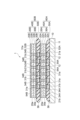
- FIG. 1 is a cross-sectional view schematically showing a semiconductor device according to an embodiment of the present disclosure.
- FIG. 2 is a plan view of the semiconductor device shown in FIG. 1 viewed from above.
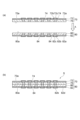
- FIGS. 3A and 3B are cross-sectional views sequentially showing a method for manufacturing the semiconductor device shown in FIG.
- FIGS. 4A and 4B are cross-sectional views sequentially showing a method for manufacturing the semiconductor device shown in FIG. 1, and are diagrams showing a process subsequent to the process shown in FIG. 3.
- FIGS. 5A and 5B are cross-sectional views sequentially showing a method for manufacturing the semiconductor device shown in FIG. 1, and are diagrams showing a process subsequent to the process shown in FIG. 4.
- FIGS. 6A and 6B are cross-sectional views sequentially showing a method for manufacturing the semiconductor device shown in FIG. 1, and are diagrams showing steps subsequent to the step shown in FIG. 5.
- FIGS. 7A to 7C are cross-sectional views sequentially showing a method for manufacturing a semiconductor device according to comparison.
- FIGS. 8A and 8B are cross-sectional views sequentially showing a method for manufacturing a semiconductor device according to a comparative example, and are diagrams showing a process subsequent to the process shown in FIG. 7.
- the term “layer” includes a structure that is formed on the entire surface as well as a structure that is formed on a part of the layer when observed as a plan view.
- the term “process” does not only refer to an independent process, but also refers to a process that cannot be clearly distinguished from other processes, as long as the intended effect of the process is achieved. included.
- a numerical range indicated using “ ⁇ ” indicates a range that includes the numerical values written before and after " ⁇ " as the minimum and maximum values, respectively.
- FIG. 1 is a cross-sectional view schematically showing an example of a semiconductor device according to this embodiment.
- the semiconductor device 1 is an example of a semiconductor package, and includes a substrate 10, a set of a first hybrid bonding structure component 40A and a first bump connection component 50A arranged on the substrate 10, Another set of a second hybrid bonding structure component 40B and a second bump connection component 50B are further disposed on the first hybrid bonding structure component 40A and the first bump connection component 50A.
- a first bump connection component 50A, a first hybrid bonding structure component 40A, a second bump connection component 50B, and a second hybrid bonding structure component 40B are stacked in this order on a substrate 10. There is.
- a fillet 56 is formed in which the adhesive film members 52A and 52B of the first bump connection component 50A and the second bump connection component 50B protrude outward from the end portions.
- Each fillet 56 is formed so as not to stick to each other in the stacking direction.
- the substrate 10 has a plurality of wiring electrodes 12 on the surface 11.
- the substrate 10 is not particularly limited as long as it is a printed circuit board, and there is no need for a metal layer formed on the surface of an insulating substrate whose main component is glass epoxy, polyimide, polyester, ceramic, epoxy, bismaleimide triazine, polyimide, etc.
- a circuit board or the like on which wiring (wiring pattern) is formed by printing can be used.
- the wiring electrode 12 includes, for example, gold, silver, and copper.
- a first hybrid bonding laminate component 60A consisting of a first hybrid bonding structural component 40A and a first bump connection component 50A is arranged on the substrate 10.
- the first hybrid bonding structure component 40A is attached to the substrate 10 by a first bump connection component 50A.
- the first hybrid bonding structure component 40A includes a first semiconductor component 26A including a first semiconductor chip 20A, a first insulating film 22A provided on the first semiconductor chip 20A, and a plurality of first electrodes 24A, and a second semiconductor component 26A. It has a chip 30A, a second semiconductor component 36A including a second insulating film 32A provided on the second semiconductor chip 30A, and a plurality of second electrodes 34A.
- a first insulating film 22A and a second insulating film 32A are bonded together, and a plurality of first electrodes 24A and a plurality of second electrodes 34 are respectively bonded.
- the first semiconductor chip 20A and the second semiconductor chip 30A are not particularly limited, and various semiconductors such as elemental semiconductors made of the same type of elements such as silicon and germanium, and compound semiconductors such as gallium arsenide and indium phosphide. can be used.
- the first semiconductor chip 20 and the second semiconductor chip 30A may have terminal electrodes 21a, 31a for connecting the semiconductor chips to the outside, and through electrodes 21b, 31b penetrating the semiconductor chips.
- the terminal electrode 21a of the first semiconductor chip 20A is connected to the terminal electrode 31a of the fourth semiconductor chip 30B via a second connection bump 54B, which will be described later.
- the through electrode 21b of the first semiconductor chip 20A is connected to the terminal electrode 21a and the first electrode 24A.
- the terminal electrode 31a of the second semiconductor chip 30A is connected to the wiring electrode 12 of the substrate 10 via the first connection bump 54A.
- the through electrode 31b of the second semiconductor chip 30A is connected to the terminal electrode 31a and the second electrode 34A.
- the thickness of the first semiconductor chip 20A and the second semiconductor chip 30A is, for example, in the range of 0.2 mm to 2.0 mm.
- the first insulating film 22A and the second insulating film 32A are configured to include an inorganic insulating material or an organic insulating material.
- the first insulating film 22A and the second insulating film 32A may be configured to include both an inorganic insulating material and an organic insulating material.
- the inorganic insulating material used for the insulating film is, for example, silicon oxide (SiO 2 ).
- SiO 2 silicon oxide
- an inorganic insulating material such as silicon oxide is used for the insulating film, a semiconductor device with a finer structure can be manufactured. Further, since the bond between inorganic insulating materials can be easily made strong, it is possible to increase the adhesive strength between semiconductor chips and improve the connection reliability as a semiconductor device.
- the organic insulating material used for the first insulating film 22A and the second insulating film 32A is, for example, polyimide, polyimide precursor (for example, polyimiamic ester or polyamic acid), polyamideimide, benzocyclobutene (BCB), polybenzoxazole ( PBO) or PBO precursor.
- These organic insulating materials have a lower elastic modulus than inorganic insulating materials such as silicon oxide (SiO 2 ), and are soft materials.
- the elastic modulus of the organic material constituting the first insulating film 22A and the second insulating film 32A may be, for example, 7.0 GPa or less, 5.0 GPa or less, or 3.0 GPa or less. It may be 2.0 GPa or less, or 1.5 GPa or less.
- the elastic modulus here means Young's modulus.
- the organic insulating material constituting the first insulating film 22A and the second insulating film 32A preferably has a coefficient of thermal expansion of 70 ppm/K or less, and more preferably 50 ppm/K or less.
- the thickness of the first insulating film 22A and the second insulating film 32A is preferably 10 ⁇ m or less, more preferably 5 ⁇ m or less, and even more preferably 3 ⁇ m or less.
- the thickness of the first insulating film 22A and the second insulating film 32A is preferably 1 ⁇ m or more from the viewpoint of ensuring electrical reliability.
- the first electrode 24A and the second electrode 34A are terminal electrodes provided on the inner surfaces 20a and 30a of the first semiconductor chip 20A and the second semiconductor chip 30A, and are made of copper or aluminum, for example.
- the first electrode 24A penetrates the first insulating film 22A and is exposed on the surface of the first insulating film 22A that is opposite to the surface 20a to which the first semiconductor chip 20A is connected.
- the second electrode 34A penetrates the second insulating film 32A and is exposed on the surface of the second insulating film 32A that is opposite to the surface 30a to which the second semiconductor chip 30A is connected.
- the first electrode 24A and the second electrode 34A are bonded to each other.
- the first bump connection component 50A to which the first hybrid bonding structure component 40A is attached is the first adhesive film member 52A attached to the surface of the second semiconductor chip 30A opposite to the second insulating film 32A. and a first connection bump 54A disposed in the first adhesive film member 52A and flip-chip connected to the terminal electrode 31a of the second semiconductor chip 30A.
- the first connection bump 54A contains gold, silver, copper, solder (main components are, for example, tin-silver, tin-lead, tin-bismuth, tin-copper), nickel, tin, lead, etc. as main components. and may contain multiple metals.
- the first adhesive film member 52A contains an epoxy resin, a thermoplastic resin, a curing agent, a fluxing agent, and an inorganic filler.
- the first adhesive film member 52A may be an insulating resin layer containing no conductive filler (conductive particles).
- the first adhesive film member 52A is a cured product of a resin composition containing the above-mentioned epoxy resin, thermoplastic resin, curing agent, fluxing agent, and inorganic filler.
- Such a first adhesive film member 52A can be formed using, for example, NCF (Non Conductive Film).
- a second hybrid bonding laminate component 60B consisting of a second hybrid bonding structural component 40B and a second bump connection component 50B is arranged on the first hybrid bonding laminate component 60A having such a configuration, and A bonding structure component 40B is attached to the first semiconductor chip 20A of the first hybrid bonding laminate component 60A by a second bump connection component 50B.
- the second hybrid bonding laminate component 60B has the same configuration as the first hybrid bonding laminate component 60A, and hereinafter, some overlapping parts may be omitted in the description.
- the second hybrid bonding structure component 40B includes a third semiconductor component 26B including a third semiconductor chip 20B, a third insulating film 22B provided on the third semiconductor chip 20B, and a plurality of third electrodes 24B, and a fourth semiconductor component 26B. It has a chip 30B, a fourth semiconductor component 36B including a fourth insulating film 32B provided on the fourth semiconductor chip 30B, and a plurality of fourth electrodes 34B.
- the third insulating film 22B and the fourth insulating film 32B are bonded together, and the plurality of third electrodes 24B and the plurality of fourth electrodes 34B are respectively bonded.
- the third semiconductor chip 20B and the fourth semiconductor chip 30B are the same semiconductor chips as the first semiconductor chip 20A and the second semiconductor chip 30A.
- the third semiconductor chip 20B and the fourth semiconductor chip 30B may have terminal electrodes 21a, 31a for connecting the semiconductor chips to the outside, and through electrodes 21b, 31b penetrating the semiconductor chips.
- the terminal electrode 31a of the fourth semiconductor chip 30B is connected to the terminal electrode 21a of the first semiconductor chip 20A via the second connection bump 54B.
- the through electrode 31b of the fourth semiconductor chip 30B is connected to the terminal electrode 31a and the fourth electrode 34B.
- the thickness of the third semiconductor chip 20B and the fourth semiconductor chip 30B is, for example, in the range of 0.2 mm to 2.0 mm, similarly to the first semiconductor chip 20A and the like.
- the third insulating film 22B and the fourth insulating film 32B are configured to include an inorganic insulating material or an organic insulating material, similarly to the first insulating film 22A and the second insulating film 32A.
- the third insulating film 22B and the fourth insulating film 32B may be configured to include both an inorganic insulating material and an organic insulating material.
- the inorganic insulating material or organic insulating material used for the insulating film is the same as that for the first insulating film 22A.
- the thicknesses of the third insulating film 22B and the fourth insulating film 32B are similarly preferably 10 ⁇ m or less, more preferably 5 ⁇ m or less, and even more preferably 3 ⁇ m or less.
- the thickness of the third insulating film 22B and the fourth insulating film 32B is preferably 1 ⁇ m or more from the viewpoint of ensuring electrical reliability.
- the third electrode 24B and the fourth electrode 34B are terminal electrodes provided on the inner surfaces 20a and 30a of the third semiconductor chip 20B and the fourth semiconductor chip 30B, and are made of copper or aluminum, for example.
- the third electrode 24B penetrates the third insulating film 22B and is exposed on the surface of the third insulating film 22B that is opposite to the surface 20a to which the third semiconductor chip 20B is connected.
- the fourth electrode 34B penetrates the fourth insulating film 32B and is exposed on a surface of the fourth insulating film 32B opposite to the surface 30a to which the fourth semiconductor chip 30B is connected.
- the third electrode 24B and the fourth electrode 34B are bonded to each other.
- the second bump connection component 50B attached to the second hybrid bonding structure component 40B is attached to the surface of the fourth semiconductor chip 30B opposite to the fourth insulating film 32B, similarly to the first bump connection component 50A.
- a second adhesive film member 52B is attached thereto, and a second connection bump 54B is disposed in the second adhesive film member 52B and is flip-chip connected to the terminal electrode 31a of the fourth semiconductor chip 30B.
- the second connection bump 54B contains gold, silver, copper, solder (main components are, for example, tin-silver, tin-lead, tin-bismuth, tin-copper), nickel, tin, lead, etc. as main components. and may contain multiple metals.
- a first hybrid bonding laminate component 60A which is a pair of a first hybrid bonding structure component 40A and a first bump connection component 50A, is arranged on the substrate 10.
- the wiring electrode 12 of the substrate 10 is connected to the terminal electrode 31a of the second semiconductor chip 30A of the first hybrid bonding structure component 40A via the first connection bump 54A.
- This terminal electrode 31a is connected to the terminal electrode 21a of the first semiconductor chip 20A via the second electrode 34A, the first electrode 24A, and the through electrode 21b of the first semiconductor chip 20A.
- a second hybrid bonding laminate component 60B which is a pair of a second hybrid bonding structure component 40B and a second bump connection component 50B, is further arranged.
- the terminal electrode 21a of the first semiconductor chip 20A is connected to the terminal electrode 31a of the fourth semiconductor chip 30B of the second hybrid bonding structure component 40B via the second connection bump 54B.
- This terminal electrode 31a is connected to the through electrode 21b of the third semiconductor chip 20B via the fourth electrode 34B and the third electrode 24B.
- the semiconductor device 1 has a structure in which hybrid bonding structural components and bump connection components including adhesive film members are alternately laminated.
- FIG. 2 is a plan view of the semiconductor device 1 viewed from above.
- the fillet 56 is an adhesive portion that protrudes outward from the entire outer periphery of the semiconductor chip (for example, the third semiconductor chip 20B), and This is a portion that can protect the semiconductor chip 30A, the third semiconductor chip 20B, and the fourth semiconductor chip 30B.
- the maximum value of the protrusion width T of the fillet 56 may be, for example, less than half the thickness (height) of the first hybrid bonding structure component 40A or the second hybrid bonding structure component 40B.
- FIGS. 3A and 3B are cross-sectional views sequentially showing a method for manufacturing the semiconductor device shown in FIG.
- FIGS. 4A and 4B are cross-sectional views sequentially showing a method for manufacturing the semiconductor device shown in FIG. 1, and are diagrams showing a process subsequent to the process shown in FIG. 3.
- FIGS. 5A and 5B are cross-sectional views sequentially showing a method for manufacturing the semiconductor device shown in FIG. 1, and are diagrams showing a process subsequent to the process shown in FIG. 4.
- 6A and 6B are cross-sectional views sequentially showing a method for manufacturing the semiconductor device shown in FIG. 1, and are diagrams showing steps subsequent to the step shown in FIG. 5.
- the semiconductor device 1 can be manufactured, for example, through the following steps (a) to (h).
- Step (a) corresponds to a plurality of semiconductor components including the first semiconductor component 26A and the third semiconductor component 26B, and is a first silicon substrate on which an integrated circuit including semiconductor elements and wiring connecting them is formed.
- This is a step of preparing the semiconductor substrate 70.
- a plurality of first electrodes 74 made of copper, aluminum, etc. are provided at predetermined intervals on one surface 72a of the first substrate body 72 made of silicon etc.
- a first insulating film 76 made of an inorganic or organic material is provided.
- the first substrate body 72 may be, for example, a circular or rectangular semiconductor wafer.
- the first electrode 74 is an end face electrode for penetrating the first insulating film 76 and exposing the integrated circuit formed on the first semiconductor substrate 70 to the outside.
- the plurality of first electrodes 74 may be provided after the first insulating film 76 is provided on the one surface 72a of the first substrate main body 72, or the plurality of first electrodes 74 may be provided on the one surface 72a of the first substrate main body 72.
- the first insulating film 76 may be provided after that.
- the first substrate body 72 may be provided with a terminal electrode 72b connected to an integrated circuit or the like and a through electrode 72c penetrating the substrate body.
- Step (b) corresponds to a plurality of semiconductor components including the second semiconductor component 36A and the fourth semiconductor component 36B, and is a second silicon substrate on which an integrated circuit including semiconductor elements and wiring connecting them is formed.
- This is a step of preparing the semiconductor substrate 80.
- a plurality of second electrodes 84 made of copper, aluminum or the like are provided at predetermined intervals on one surface 82a of the second substrate main body 82 made of silicon or the like.
- a second insulating film 86 made of an inorganic or organic material is provided.
- the second substrate body 82 may be, for example, a circular or rectangular semiconductor wafer.
- the second electrode 84 is an end face electrode for penetrating the second insulating film 86 and exposing the integrated circuit formed on the second semiconductor substrate 80 to the outside.
- the plurality of second electrodes 84 may be provided after the second insulating film 86 is provided on the one surface 82a of the second substrate main body 82, or the plurality of second electrodes 84 may be provided on the one surface 82a of the second substrate main body 82. Alternatively, the second insulating film 86 may be provided.
- the first insulating film 76 and the second insulating film 86 used in step (a) and step (b) are the first insulating film 22A, second insulating film 32A, third insulating film 22B, and fourth insulating film 32B described above. It is made up of inorganic or organic materials.
- the inorganic material used for the insulating film is, for example, silicon oxide (SiO 2 ). When an inorganic material such as silicon oxide is used for the insulating film, a semiconductor device with a finer structure can be manufactured.
- step (c) described below since the bond between inorganic materials is easy to strengthen, the adhesive strength between semiconductor substrates is increased and the connection reliability as a semiconductor device is improved. becomes possible.
- the organic material used for the insulating film is, for example, polyimide, a polyimide precursor (eg, polyimiamic ester or polyamic acid), polyamideimide, benzocyclobutene (BCB), polybenzoxazole (PBO), or a PBO precursor.
- These organic materials have a lower elastic modulus than inorganic materials such as silicon oxide (SiO 2 ), and are soft materials.
- the elastic modulus of the organic material constituting the first insulating film 76 and the second insulating film 86 may be, for example, 7.0 GPa or less, 5.0 GPa or less, or 3.0 GPa or less. It may be 2.0 GPa or less, or 1.5 GPa or less.
- the elastic modulus here means Young's modulus.
- the organic material constituting the first insulating film 76 and the second insulating film 86 preferably has a coefficient of thermal expansion of 70 ppm/K or less, and more preferably 50 ppm/K or less.
- each insulating film can be easily formed as a thin film by spin coating or the like. Furthermore, since these organic materials have heat resistance, they can withstand the temperature (for example, a high temperature of 300° C. or higher) when the first electrode 74 and the second electrode 84 are bonded in step (c) described later. This prevents the bond between the insulating films from deteriorating due to high temperatures.
- the first insulating film 76 and the second insulating film 86 may be insulating films containing both an inorganic material and an organic material.
- the thickness of the first insulating film 76 and the second insulating film 86 may be 20 ⁇ m or less. By sufficiently reducing the thickness of the first insulating film 76 and the second insulating film 86, the wiring formed from the first electrode 74 and the second electrode 84 can have a finer structure. Note that the thickness of the first insulating film 76 and the second insulating film 86 may be thicker than 20 ⁇ m. In this case, when the insulating films are bonded together, more debris can be embedded in the resin insulating film, and the insulating films can be bonded together more reliably. Further, the thickness of the first insulating film 76 and the second insulating film 86 may be 4 ⁇ m or more. In this case, by embedding minute debris in the resin insulating film, even if minute debris remains, it is possible to maintain a good connection between the first insulating film 76 and the second insulating film 86. It becomes possible.
- step (c) the first insulating film 76 of the first semiconductor substrate 70 and the second insulating film 86 of the second semiconductor substrate 80 are bonded together, and the plurality of first electrodes 74 of the first semiconductor substrate 70 and the first insulating film 86 of the second semiconductor substrate 80 are bonded together.
- the bonding surface 70a of the first semiconductor substrate 70 and the bonding surface 80a of the second semiconductor substrate 80 are polished using a CMP (Chemical Mechanical Polishing) method.
- CMP Chemical Mechanical Polishing
- the first semiconductor substrate 70 may be polished by a CMP method under the condition that the first electrode 74 made of copper or the like is selectively and deeply removed, or each surface of the first electrode 74 is aligned with the surface of the first insulating film 76. It may be polished by CMP method. The same applies to the polishing of the second semiconductor substrate 80. Such polishing also removes debris on the surfaces of the first semiconductor substrate 70 and the second semiconductor substrate 80.
- step (c) after removing the organic substances or metal oxides attached to the surfaces of the bonding surface 70a of the first semiconductor substrate 70 and the bonding surface 80a of the second semiconductor substrate 80, the steps shown in FIGS. 3A and 3B are performed. , the bonding surface 70a of the first semiconductor substrate 70 and the bonding surface 80a of the second semiconductor substrate 80 are made to face each other, and the first electrode 74 and the second electrode 84 of the first semiconductor substrate 70 are aligned. conduct. At this positioning stage, the first insulating film 76 of the first semiconductor substrate 70 and the second insulating film 86 of the second semiconductor substrate 80 are separated from each other and are not bonded.
- the first insulating film 76 of the first semiconductor substrate 70 and the second insulating film 86 of the second semiconductor substrate 80 are bonded.
- the first insulating film 76 and the second insulating film 86 may be uniformly heated before joining.
- the heating temperature when bonding the first insulating film 76 and the second insulating film 86 may be, for example, 30° C. or more and 400° C. or less, and the pressure may be 0.1 MPa or more and 1 MPa or less.
- the first insulating film 76 and the second insulating film 86 are bonded to form an insulating bonded portion, and the first semiconductor substrate 70 and the second semiconductor substrate 80 are mechanically strengthened to each other. It is attached.
- a predetermined heat, pressure, or both are applied to bond the first electrode 74 of the first semiconductor substrate 70 and the second electrode 84 of the second semiconductor substrate 80.
- the heating temperature is 150°C or more and 400°C or less, and may be 200°C or more and 300°C or less, and the pressure is 0.1 MPa or more and 1 MPa or more. The following may be sufficient.
- the first electrode 74 and the corresponding second electrode 84 are bonded to form an electrode bonding portion, and the first electrode 74 and the second electrode 84 are mechanically and electrically bonded firmly.
- Ru Note that electrode bonding may be performed after bonding the insulating film, but electrode bonding and bonding of the insulating film may be performed simultaneously. Through the above steps, a hybrid bonding structure S is obtained.
- connection bumps 54 are formed on the surface 82d of the second substrate main body 82 of the hybrid bonding structure S opposite to the second insulating film 86.
- the connection bumps 54 mainly contain gold, silver, copper, solder (main components are, for example, tin-silver, tin-lead, tin-bismuth, tin-copper), nickel, tin, lead, etc. It may contain multiple metals.
- such connection bumps 54 are formed so as to be connected to the plurality of connection terminals 82b of the second substrate body 82.
- a conventional manufacturing method can be used.
- step (e) after the plurality of connection bumps 54 are formed in step (d), as shown in FIG.
- An adhesive film member 52 is attached to the. By this bonding, a plurality of connection bumps 54 are located within the adhesive film member 52.
- the plurality of connection bumps 54 may or may not be exposed from the surface of the adhesive film member 52.
- the adhesive film member 52 used here corresponds to the first adhesive film member 52A and the second adhesive film member 52B described above, and contains an epoxy resin, a thermoplastic resin, a curing agent, a flux agent, and an inorganic filler. do.
- the adhesive film member 52 may be an insulating resin layer containing no conductive filler (conductive particles).
- epoxy resin is not particularly limited as long as it has an epoxy group in its molecule, but epoxy resins having two or more epoxy groups in its molecule can be preferably used.
- epoxy resins include bisphenol A epoxy resin, bisphenol F epoxy resin, naphthalene epoxy resin, phenol novolac epoxy resin, cresol novolac epoxy resin, phenol aralkyl epoxy resin, biphenyl epoxy resin, Triphenolmethane type epoxy resin, dicyclopentadiene type epoxy resin; these polyfunctional epoxy resins can be mentioned.
- the epoxy resins may be used alone or in combination of two or more. Among these, the epoxy resin preferably includes a bisphenol-type epoxy resin or a triphenolmethane-type epoxy resin.
- the epoxy resin is preferably one that can suppress decomposition and generation of volatile components during connection at high temperatures. Therefore, it is preferable to use an epoxy resin whose mass reduction rate under heating conditions during connection is 5% by mass or less. For example, if the heating temperature at the time of connection is 250°C, it is preferable to use an epoxy resin with a mass reduction rate of 5% by mass or less at 250°C, and if the heating temperature is 300°C, the mass reduction rate at 300°C is 5% by mass. It is preferable to use the following epoxy resins.
- the content of the epoxy resin is preferably 5 to 75% by mass, more preferably 10 to 55% by mass, and even more preferably 20 to 50% by mass, based on the total amount of the adhesive film member. When the content of the epoxy resin is within this range, the curability and adhesiveness tend to be better.
- Thermoplastic resins include phenoxy resins, polyimide resins, polyamide resins, polycarbodiimide resins, cyanate ester resins, acrylic resins, polyester resins, polyethylene resins, and polyester resins from the viewpoint of obtaining excellent heat resistance, film forming properties, and connection reliability. It is preferable to contain at least one selected from the group consisting of ether sulfone resin, polyetherimide resin, polyvinyl acetal resin, urethane resin, and acrylic rubber.
- the thermoplastic resin preferably contains at least one selected from the group consisting of phenoxy resin, polyimide resin, acrylic rubber, acrylic resin, cyanate ester resin, and polycarbodiimide resin.
- the weight average molecular weight of the thermoplastic resin is preferably 10,000 or more, more preferably 20,000 or more, and still more preferably 30,000 or more. When the weight average molecular weight of the thermoplastic resin is 10,000 or more, the heat resistance and film formability of the adhesive film member tend to be further improved.
- the weight average molecular weight of the thermoplastic resin is preferably 1,000,000 or less, more preferably 500,000 or less. When the weight average molecular weight of the thermoplastic resin is 1,000,000 or less, the effect of high heat resistance tends to be obtained.
- weight average molecular weight means a value measured using GPC (gel permeation chromatography) and converted using a standard polystyrene calibration curve.
- GPC gel permeation chromatography
- HCL-8320GPC HCL-8320GPC
- UV-8320 manufactured by Tosoh Corporation
- HPLC-8020 manufactured by Tosoh Corporation
- a solvent in which the measurement target is dissolved can be selected. Examples of the solvent include THF (tetrahydrofuran), DMF (N,N-dimethylformamide), DMA (N,N-dimethylacetamide), NMP (N-methyl-2-pyrrolidone), and toluene.
- the concentration of phosphoric acid should be 0.05 to 0.1 mol/L (usually 0.06 mol/L), and the concentration of LiBr should be 0.5 to 1.0 mol/L ( Normally, it may be adjusted to 0.63 mol/L).
- the mass ratio of the epoxy resin content to the thermoplastic resin content is preferably 0.01 to 20. , more preferably 0.05 to 15, still more preferably 0.1 to 10.
- the curing agent is not particularly limited, and examples thereof include imidazole curing agents, phenol resin curing agents, acid anhydride curing agents, amine curing agents, phosphine curing agents, and the like.
- the curing agent preferably contains an imidazole-based curing agent from the viewpoint of exhibiting good flux performance and improving storage stability and heat resistance of the cured product of the adhesive film.
- imidazole curing agent examples include 2-phenylimidazole, 2-phenyl-4-methylimidazole, 1-benzyl-2-methylimidazole, 1-benzyl-2-phenylimidazole, 1-cyanoethyl-2-undecylimidazole.
- 1-cyanoethyl-2-undecylimidazole, 1-cyano-2-phenylimidazole, and 1-cyanoethyl-2-undecylimidazole trimellitate are preferred from the viewpoint of superior curability, storage stability, and connection reliability.
- 1-cyanoethyl-2-phenylimidazolium trimellitate 2,4-diamino-6-[2'-methylimidazolyl-(1')]-ethyl-s-triazine, 2,4-diamino-6-[ 2'-ethyl-4'-methylimidazolyl-(1')]-ethyl-s-triazine, 2,4-diamino-6-[2'-methylimidazolyl-(1')]-ethyl-s-triazine
- the content of the curing agent is preferably 0.1 to 20 parts by weight, more preferably 0.1 to 10 parts by weight, based on 100 parts by weight of the epoxy resin.
- the content of the curing agent is 0.1 parts by mass or more based on 100 parts by mass of the epoxy resin, the curability tends to be further improved, and when the content is 20 parts by mass or less, metallic bonds are not formed. Since the adhesive film does not harden before the connection is completed, connection failures tend to be less likely to occur.
- the fluxing agent can be used without particular limitation as long as it is a compound having a carboxyl group, but a dicarboxylic acid (a compound having two carboxyl groups) is preferable. Compared with monocarboxylic acids (compounds having one carboxyl group), dicarboxylic acids are less likely to volatilize even at high temperatures during connection, and tend to be able to further suppress the generation of voids. Furthermore, when dicarboxylic acid is used, it is possible to further suppress the increase in viscosity of the adhesive film during storage, connection work, etc., compared to the case where a compound having three or more carboxyl groups is used. There is a tendency that connectivity can be further improved.
- the fluxing agent may be, for example, a dicarboxylic acid having a linear or branched alkylene group.
- dicarboxylic acids include succinic acid (melting point: 184°C), glutaric acid (melting point: 95-98°C), adipic acid (melting point: 152°C), pimelic acid (melting point: 103-105°C), Suberic acid (melting point: 141-144°C), azelaic acid (melting point: 109°C), sebacic acid (melting point: 133-137°C), undecanedioic acid (melting point: 28-31°C), dodecanedioic acid (melting point: 127 dicarboxylic acids having a linear alkylene group such as ( ⁇ 129°C); branched dicarboxylic acids having one or more hydrogen atoms at the 2- or 3-position of these dicarboxylic acids having a linear alkylene group substituted with an alkyl group; Examples
- the melting point of the fluxing agent is preferably 150°C or lower, more preferably 140°C or lower, even more preferably 130°C or lower.
- Such flux agents tend to exhibit sufficient flux performance before the curing reaction between the epoxy resin and the curing agent occurs. Therefore, by using an adhesive film containing such a fluxing agent, a semiconductor device with even better connection reliability can be manufactured.
- the fluxing agent is preferably solid at room temperature (25°C), and the melting point of the fluxing agent is preferably 25°C or higher, more preferably 50°C or higher.
- the content of the fluxing agent may be, for example, 0.5 to 10% by mass based on the total amount of the adhesive film.
- the adhesive film member By containing an inorganic filler, the adhesive film member tends to further suppress the generation of voids during connection and to further reduce the hygroscopicity of the cured adhesive film.
- the inorganic filler is preferably an insulating substance from the viewpoint of excellent insulation reliability (particularly HAST resistance).
- examples of such inorganic fillers include glass, silica, alumina, titanium oxide, carbon black, mica, and boron nitride. These may be used alone or in combination of two or more.
- the inorganic filler is preferably at least one selected from the group consisting of silica, alumina, titanium oxide, and boron nitride, and more preferably at least one selected from the group consisting of silica, alumina, and boron nitride. be. These shapes and particle sizes are not particularly limited.
- the inorganic filler may be surface-treated.
- the content of the inorganic filler is preferably 20 to 70% by mass, more preferably 25 to 65% by mass, and even more preferably 30 to 60% by mass, based on the total amount of the adhesive film member.
- the adhesive film tends to have a smooth appearance and the components tend to be easily dispersed.
- the adhesive film may further contain a resin filler.
- the resin filler include fillers made of resin such as polyurethane and polyimide.
- the content of the resin filler is preferably 1 to 30% by mass, more preferably 2 to 30% by mass, and even more preferably 3 to 15% by mass, based on the total amount of the adhesive film.
- the adhesive film member may further contain a curing accelerator, a silane coupling agent, a titanium coupling agent, an antioxidant, a leveling agent, an ion trapping agent, etc. as other components.
- the content of the other components can be adjusted as appropriate so that each component exhibits its effects, and may be, for example, 0.1 to 20% by mass, respectively, based on the total amount of the adhesive film.
- the adhesive film member can be formed, for example, by the following method. First, an organic solvent is added as necessary to a resin composition containing the above-mentioned components constituting the adhesive film, and a resin composition varnish obtained by stirring, mixing, kneading, etc. is applied to a base film that has been subjected to a release treatment. Apply on top using a knife coater, roll coater, applicator, etc. Thereafter, by heating the applied resin composition varnish to remove the organic solvent, an adhesive film can be formed on the base film.
- the organic solvent used for preparing the resin composition varnish is not particularly limited as long as it has the property of uniformly dissolving or dispersing each component, but examples include dimethylformamide, dimethylacetamide, and N-methyl-2-pyrrolidone. , dimethyl sulfoxide, diethylene glycol dimethyl ether, toluene, benzene, xylene, methyl ethyl ketone, tetrahydrofuran, ethyl cellosolve, ethyl cellosolve acetate, butyl cellosolve, dioxane, cyclohexanone, ethyl acetate and the like. These organic solvents can be used alone or in combination of two or more. Among these, it is preferable that the organic solvent contains methyl ethyl ketone.
- Stirring, mixing, kneading, etc. in the preparation of the resin composition varnish can be performed using, for example, a stirrer, a miller, a three-roll mill, a ball mill, a bead mill, a homodisper, or the like.
- the base film is not particularly limited as long as it has heat resistance that can withstand the heating conditions when drying the organic solvent.
- Examples of the base film include polyolefin films such as polypropylene films and polymethylpentene films, polyester films such as polyethylene terephthalate films and polyethylene naphthalate films, polyimide films, and polyetherimide films.
- the base film may be a monolayer film of one type alone, or a multilayer film of a combination of two or more types.
- the thickness of the adhesive film obtained can be adjusted, for example, based on the height of the bump before connection, and is preferably 0.5 to 1.5 times, or more, based on the height of the bump before connection. It is preferably 0.6 to 1.3 times, more preferably 0.7 to 1.2 times.
- the thickness of the adhesive film is 0.5 times or more the height of the bump, the generation of voids due to unfilled adhesive film can be sufficiently suppressed, and connection reliability can be further improved.
- the thickness of the adhesive film is 1.5 times or less, the amount of adhesive film extruded from the chip connection area during connection can be sufficiently suppressed, and furthermore, the adhesive film can be sufficiently prevented from adhering to unnecessary parts. can be prevented.
- the thickness of the adhesive film is preferably 2.5 to 150 ⁇ m, more preferably 3.5 to 120 ⁇ m.
- the drying conditions for volatilizing the organic solvent from the resin composition varnish applied to the base film are not particularly limited as long as the organic solvent is sufficiently volatilized. Heating is preferred.
- the organic solvent is preferably removed to 1.5% by mass or less based on the total amount of the adhesive film.
- step (f) the hybrid bonding structure S to which the adhesive film member 52 made of the above-mentioned material is bonded is diced, and at least one first semiconductor element, at least one first electrode 74, and at least one first semiconductor element are diced.
- a plurality of hybrid bonding laminate components 60 are obtained, each of which includes two semiconductor elements, at least one second electrode 84, and at least one connection bump 54.
- the hybrid bonding structure S to which the adhesive film member 52 has been bonded is diced using plasma dicing, stealth dicing, laser dicing, or the like to separate the hybrid bonding structure S into individual pieces.
- individual hybrid bonding laminate parts 60 are obtained as shown in FIG. 5(a).
- This hybrid bonding laminate component 60 corresponds to the first hybrid bonding laminate component 60A and the second hybrid bonding laminate component 60B described above.
- step (g) a plurality of individualized hybrid bonding laminate parts 60 are stacked and bonded together.
- step (g) first, as shown in FIG. 5B, the first hybrid bonding laminate component 60A is picked up by the bonding tool P and moved toward the substrate 10. Thereafter, after placing the first hybrid bonding laminate component 60A on the substrate 10, the first hybrid bonding laminate component 60A is pressed while being heated. At this time, as shown in FIG. 6A, each of the first connection bumps 54A and the corresponding wiring electrode 12 are connected. In other words, the terminal electrode 31a of the second semiconductor chip 30A is connected to the wiring electrode 12 via the first connection bump 54A. Further, during this pressing, the first adhesive film member 52A protrudes outward from the end of the second semiconductor chip 30A to form a fillet 56. The protrusion width of this fillet 56 is the same as the protrusion width T mentioned above.
- the second hybrid bonding laminate component 60B is picked up by the bonding tool P, and the second hybrid bonding laminate component 60B is placed on the first hybrid bonding laminate component 60A. Press the second hybrid bonding laminate component 60B. At this time, the terminal electrode 31a of the fourth semiconductor chip 30B is connected to the terminal electrode 21a of the first semiconductor chip 20A via the second connection bump 54B. Further, the second bump connection component 50B is attached to the first semiconductor chip 20A.
- FIG. 7A a member 160 is provided with connection bumps 152 and 154 on the lower surface of the semiconductor chip 120, and an adhesive film member 150 is attached to the semiconductor chip 120 so as to cover the connection bumps 152 and 154.
- the adhesive film member 150 corresponds to the adhesive film member 50 and the like.
- Such a member is picked up by the bonding tool P, moved toward the substrate 110, and the connection bumps 152, 154 and the connection terminal 112 are connected as shown in FIG. 7(b). This connection causes the ends of the adhesive film member 150 to protrude outward, forming a fillet 156.
- such members 160 are stacked to fabricate the semiconductor device 101.
- fillets 156 are formed, but fillets 156 adjacent in the stacking direction stick to each other.
- a gap V which is a closed space, is formed between the fillets 156.
- the first hybrid bonding structural component uses a hybrid bonding technique in which semiconductor chips (or semiconductor wafers, etc.) are bonded together and connected without using a general adhesive. 40A, and a first bump connection component 50A having a first adhesive film member 52A. According to this configuration, it is possible to sandwich (interpose) the first hybrid bonding structural component 40A between the adhesive film members, so it is possible to suppress the fillets 56 from sticking together. This suppresses the formation of a gap in the fillet 56 of the semiconductor device, and prevents peeling starting from the gap. As described above, according to this semiconductor device 1, the reliability of the device can be improved.
- the height can be made lower than when connecting using bumps or the like, so the height of the semiconductor device 1 can be reduced.
- the fillet 56 can be provided on the outside of the semiconductor chip using the adhesive film member 52, it is possible to protect the semiconductor chip in the semiconductor device 1. As described above, according to this semiconductor device 1, it is possible to reduce the height and improve the protection function.
- the semiconductor device 1 further includes a substrate 10 having a wiring electrode 12, and the first connection bump 54A of the first bump connection component 50A is connected to the wiring electrode 12. According to this configuration, the first semiconductor component and the substrate can be connected more reliably.
- the first adhesive film member 52A protrudes outward from the end of the second semiconductor chip 30A to form a fillet 56.
- the semiconductor chip included in the semiconductor device 1 can be more reliably protected.
- the maximum protrusion width of the fillet 56 from the end of the second semiconductor chip 30A is preferably less than half the thickness of the first hybrid bonding structure component 40A. According to this configuration, a more reliable semiconductor device can be provided by achieving a balance between protecting the semiconductor chip and suppressing peeling.
- At least one of the first insulating film 22A and the second insulating film 32A may include an inorganic insulating material. According to this configuration, it is possible to manufacture a semiconductor device with a finer configuration. Further, since the bond between inorganic materials can be easily made strong, it is possible to increase the adhesive strength between semiconductor chips and further improve the connection reliability as a semiconductor device.
- At least one of the first insulating film 22A and the second insulating film 32A may include an organic insulating material. According to this configuration, the debris from dicing into semiconductor chips is absorbed (incorporated) into the insulating film portion made of the organic material by the organic material, which is a relatively soft material, and the semiconductors are bonded by hybrid bonding. Connection defects between chips can be reduced.
- the organic insulating material included in at least one of the first insulating film 22A and the second insulating film 32A is polyimide, a polyimide precursor, polyamideimide, benzocyclobutene (BCB), polybenzoxazole (PBO), Or it may contain a PBO precursor. Since these materials are liquid or soluble in a solvent, the first insulating film and the like can be easily formed by, for example, spin coating, making it easier to form a thin film. Further, since these materials have high heat resistance, they can withstand high temperatures when bonding is performed by hybrid bonding, and it becomes possible to bond semiconductor chips together more reliably.
- the first adhesive film member 52A preferably includes a cured product of a resin composition containing an epoxy resin, a thermoplastic resin, a curing agent, and an inorganic filler. According to this configuration, the first hybrid bonding structural component 40A and the like can be bonded more reliably, and the reliability of the semiconductor device can be improved.
- the present invention is not limited to the above embodiments.
- an example was shown in which two sets of hybrid bonding laminate components 60 were stacked, but the present invention is not limited to this.
- a semiconductor device may be formed by stacking three or more sets of hybrid bonding laminate components 60.
- SYMBOLS 1...Semiconductor device 10...Substrate, 12...Wiring electrode, 20A...First semiconductor chip, 20B...Third semiconductor chip, 21a...Terminal electrode, 21b...Through electrode, 22A...First insulating film, 22B...Third insulation Film, 24A...first electrode, 24B...third electrode, 26A...first semiconductor component, 26B...third semiconductor component, 30A...second semiconductor chip, 30B...fourth semiconductor chip, 31a...terminal electrode, 31b...penetration Electrode, 32A...second insulating film, 32B...fourth insulating film, 34A...second electrode, 34B...fourth electrode, 36A...second semiconductor component, 36B...fourth semiconductor component, 40A...first hybrid bonding structure component , 40B...Second hybrid bonding structural component, 50A...First bump connection component, 50B...Second bump connection component, 52A...First adhesive film member, 52B...Second adhesive film member, 54A...First connection bump, 54
Landscapes
- Wire Bonding (AREA)
Priority Applications (4)
| Application Number | Priority Date | Filing Date | Title |
|---|---|---|---|
| US18/857,184 US20250273610A1 (en) | 2022-04-22 | 2022-04-22 | Semiconductor apparatus and method for manufacturing semiconductor apparatus |
| PCT/JP2022/018580 WO2023203764A1 (ja) | 2022-04-22 | 2022-04-22 | 半導体装置、及び、半導体装置の製造方法 |
| JP2024516044A JP7827136B2 (ja) | 2022-04-22 | 2022-04-22 | 半導体装置、及び、半導体装置の製造方法 |
| CN202280095053.9A CN119096341A (zh) | 2022-04-22 | 2022-04-22 | 半导体装置及半导体装置的制造方法 |
Applications Claiming Priority (1)
| Application Number | Priority Date | Filing Date | Title |
|---|---|---|---|
| PCT/JP2022/018580 WO2023203764A1 (ja) | 2022-04-22 | 2022-04-22 | 半導体装置、及び、半導体装置の製造方法 |
Publications (1)
| Publication Number | Publication Date |
|---|---|
| WO2023203764A1 true WO2023203764A1 (ja) | 2023-10-26 |
Family
ID=88419484
Family Applications (1)
| Application Number | Title | Priority Date | Filing Date |
|---|---|---|---|
| PCT/JP2022/018580 Ceased WO2023203764A1 (ja) | 2022-04-22 | 2022-04-22 | 半導体装置、及び、半導体装置の製造方法 |
Country Status (4)
| Country | Link |
|---|---|
| US (1) | US20250273610A1 (https=) |
| JP (1) | JP7827136B2 (https=) |
| CN (1) | CN119096341A (https=) |
| WO (1) | WO2023203764A1 (https=) |
Cited By (1)
| Publication number | Priority date | Publication date | Assignee | Title |
|---|---|---|---|---|
| WO2025197319A1 (ja) * | 2024-03-22 | 2025-09-25 | Rapidus株式会社 | 半導体システムおよび半導体システムの製造方法 |
Citations (3)
| Publication number | Priority date | Publication date | Assignee | Title |
|---|---|---|---|---|
| JP2012222038A (ja) * | 2011-04-05 | 2012-11-12 | Elpida Memory Inc | 半導体装置の製造方法 |
| JP2014063974A (ja) * | 2012-08-27 | 2014-04-10 | Ps4 Luxco S A R L | チップ積層体、該チップ積層体を備えた半導体装置、及び半導体装置の製造方法 |
| JP2018037687A (ja) * | 2017-11-28 | 2018-03-08 | 東芝メモリ株式会社 | 半導体装置及びその製造方法 |
-
2022
- 2022-04-22 JP JP2024516044A patent/JP7827136B2/ja active Active
- 2022-04-22 WO PCT/JP2022/018580 patent/WO2023203764A1/ja not_active Ceased
- 2022-04-22 US US18/857,184 patent/US20250273610A1/en active Pending
- 2022-04-22 CN CN202280095053.9A patent/CN119096341A/zh active Pending
Patent Citations (3)
| Publication number | Priority date | Publication date | Assignee | Title |
|---|---|---|---|---|
| JP2012222038A (ja) * | 2011-04-05 | 2012-11-12 | Elpida Memory Inc | 半導体装置の製造方法 |
| JP2014063974A (ja) * | 2012-08-27 | 2014-04-10 | Ps4 Luxco S A R L | チップ積層体、該チップ積層体を備えた半導体装置、及び半導体装置の製造方法 |
| JP2018037687A (ja) * | 2017-11-28 | 2018-03-08 | 東芝メモリ株式会社 | 半導体装置及びその製造方法 |
Cited By (1)
| Publication number | Priority date | Publication date | Assignee | Title |
|---|---|---|---|---|
| WO2025197319A1 (ja) * | 2024-03-22 | 2025-09-25 | Rapidus株式会社 | 半導体システムおよび半導体システムの製造方法 |
Also Published As
| Publication number | Publication date |
|---|---|
| JP7827136B2 (ja) | 2026-03-10 |
| JPWO2023203764A1 (https=) | 2023-10-26 |
| US20250273610A1 (en) | 2025-08-28 |
| CN119096341A (zh) | 2024-12-06 |
Similar Documents
| Publication | Publication Date | Title |
|---|---|---|
| TWI552294B (zh) | A circuit-connecting material, and a method of manufacturing the semiconductor device using the same | |
| TWI818911B (zh) | 半導體用接著劑、半導體裝置的製造方法及半導體裝置 | |
| JP2025074222A (ja) | 半導体用接着剤、並びに、半導体装置及びその製造方法 | |
| CN112771659B (zh) | 半导体用黏合剂、半导体装置的制造方法及半导体装置 | |
| JP7384171B2 (ja) | 半導体用フィルム状接着剤、半導体装置及びその製造方法 | |
| TWI834852B (zh) | 半導體用接著劑、半導體裝置的製造方法及半導體裝置 | |
| JP7827136B2 (ja) | 半導体装置、及び、半導体装置の製造方法 | |
| JP7521271B2 (ja) | 多層フィルムの製造方法、多層フィルム及び半導体装置の製造方法 | |
| JP7172167B2 (ja) | 半導体装置の製造方法、及びそれに用いられる半導体用接着剤 | |
| KR102951632B1 (ko) | 반도체 장치를 제조하는 방법, 및 필름상 접착제 | |
| TWI820200B (zh) | 半導體裝置及其製造方法 | |
| CN111801781B (zh) | 半导体用粘接剂及使用了其的半导体装置的制造方法 | |
| WO2025053180A1 (ja) | 半導体装置の製造方法、及びフィルム状接着剤 | |
| JP7238453B2 (ja) | 半導体用接着剤 | |
| KR20250067086A (ko) | 적층 필름 및 반도체 장치의 제조 방법 | |
| WO2024009498A1 (ja) | 半導体装置の製造方法、基板及び半導体素子 | |
| JP2021061276A (ja) | 半導体装置の製造方法 | |
| KR20260064704A (ko) | 반도체 장치의 제조 방법, 및 필름상 접착제 | |
| KR20250114283A (ko) | 접착제 필름, 접착제 테이프, 박리 필름 부착 접착제 테이프, 반도체 장치의 제조 방법 및 반도체 장치 |
Legal Events
| Date | Code | Title | Description |
|---|---|---|---|
| 121 | Ep: the epo has been informed by wipo that ep was designated in this application |
Ref document number: 22938563 Country of ref document: EP Kind code of ref document: A1 |
|
| WWE | Wipo information: entry into national phase |
Ref document number: 18857184 Country of ref document: US |
|
| WWE | Wipo information: entry into national phase |
Ref document number: 202280095053.9 Country of ref document: CN |
|
| WWE | Wipo information: entry into national phase |
Ref document number: 2024516044 Country of ref document: JP |
|
| NENP | Non-entry into the national phase |
Ref country code: DE |
|
| 122 | Ep: pct application non-entry in european phase |
Ref document number: 22938563 Country of ref document: EP Kind code of ref document: A1 |
|
| WWP | Wipo information: published in national office |
Ref document number: 18857184 Country of ref document: US |