WO2023199596A1 - 電子機器カバー、電子機器及び制御方法 - Google Patents
電子機器カバー、電子機器及び制御方法 Download PDFInfo
- Publication number
- WO2023199596A1 WO2023199596A1 PCT/JP2023/005647 JP2023005647W WO2023199596A1 WO 2023199596 A1 WO2023199596 A1 WO 2023199596A1 JP 2023005647 W JP2023005647 W JP 2023005647W WO 2023199596 A1 WO2023199596 A1 WO 2023199596A1
- Authority
- WO
- WIPO (PCT)
- Prior art keywords
- electronic device
- loop
- loop antenna
- magnetic flux
- device cover
- Prior art date
- Legal status (The legal status is an assumption and is not a legal conclusion. Google has not performed a legal analysis and makes no representation as to the accuracy of the status listed.)
- Ceased
Links
Images



Classifications
-
- G—PHYSICS
- G06—COMPUTING OR CALCULATING; COUNTING
- G06K—GRAPHICAL DATA READING; PRESENTATION OF DATA; RECORD CARRIERS; HANDLING RECORD CARRIERS
- G06K19/00—Record carriers for use with machines and with at least a part designed to carry digital markings
- G06K19/06—Record carriers for use with machines and with at least a part designed to carry digital markings characterised by the kind of the digital marking, e.g. shape, nature, code
- G06K19/067—Record carriers with conductive marks, printed circuits or semiconductor circuit elements, e.g. credit or identity cards also with resonating or responding marks without active components
- G06K19/07—Record carriers with conductive marks, printed circuits or semiconductor circuit elements, e.g. credit or identity cards also with resonating or responding marks without active components with integrated circuit chips
- G06K19/077—Constructional details, e.g. mounting of circuits in the carrier
-
- H—ELECTRICITY
- H01—ELECTRIC ELEMENTS
- H01Q—ANTENNAS, i.e. RADIO AERIALS
- H01Q7/00—Loop antennas with a substantially uniform current distribution around the loop and having a directional radiation pattern in a plane perpendicular to the plane of the loop
Definitions
- the present disclosure relates to an electronic device cover that can be attached to an electronic device having a loop antenna, an electronic device having the loop antenna, and a control method.
- Patent Document 1 proposes a booster antenna that extends the communication distance in the magnetic flux direction of a loop antenna.
- the user may bring a different part of the electronic device close to the reader/writer terminal, rather than the part on which the loop antenna is mounted.
- electronic devices such as smartphones used by multiple users exchange data using NFC
- the distance and orientation between the electronic devices depends on each user, and the portions of the electronic devices equipped with loop antennas do not face each other properly.
- An electronic device cover includes: The electronic device has a first loop antenna having a first loop portion and a first magnetic flux penetration region that is provided inside the first loop portion and allows magnetic flux to penetrate in the thickness direction of the electronic device.
- a second loop portion at least a portion of which faces the first loop portion in the thickness direction and magnetically couples with the first loop antenna; a second magnetic flux penetration region that is provided inside the second loop portion and allows the magnetic flux to penetrate in the thickness direction;
- a third loop part that spreads out, A second loop antenna is provided.
- the second loop portion of the second loop antenna faces the first loop antenna in the Z direction
- the third loop portion of the second loop antenna faces the first loop antenna in the Z direction. does not face the first loop antenna in the Z direction but spreads in the XY directions.
- This increases the magnetic coupling between the magnetic fluxes of the first loop antenna and the second loop antenna in the Z direction, expanding the communication range of the main surface and the touch panel surface in the Z direction, and at the same time, the communication range of the first loop antenna and the second loop antenna increases. It is possible to stably expand the communication range in the X and Y directions.
- the magnetic sheet may further include a magnetic sheet having the following.
- the magnetic flux of the first loop antenna and the magnetic flux of the second loop portion of the second loop antenna are magnetically coupled via the non-magnetic portion of the second magnetic sheet.
- it is possible to increase the magnetic coupling between the magnetic fluxes of the first loop antenna and the second loop antenna in the Z direction, and to expand the communication range of the main surface and the touch panel surface in the Z direction.
- the third loop portion of the second loop antenna faces the non-magnetic portion of the second magnetic sheet in the Z direction, cancellation of the magnetic flux generated in the third loop portion can be prevented, and the magnetic flux is stabilized.
- the communication range of the first loop antenna in the X and Y directions can be stably expanded.
- the non-magnetic portion may be a region obtained by cutting out the magnetic sheet.
- the non-magnetic portion may be a region obtained by cutting out the second magnetic sheet, that is, an air layer. Therefore, the second magnetic sheet including the non-magnetic portion can be manufactured easily and inexpensively, and the weight can be reduced.
- the innermost line of the first loop portion may face at least a portion of the second loop portion in the thickness direction.
- the innermost line of the second loop portion may face the first magnetic flux penetration region in the thickness direction.
- the boundary of the non-magnetic part and the outermost line of the second loop part are spaced apart in the direction of the main surface, When the electronic device cover is attached to the electronic device, a boundary of the non-magnetic portion and an outermost line of the first loop antenna may be separated from each other in the direction of the main surface.
- the electronic device may apply power to the first loop antenna when the electronic device cover is attached to the electronic device, and apply power to the first loop antenna when the electronic device cover is not attached to the electronic device.
- the antenna may further include a first control circuit that applies a power higher than the power applied to the loop antenna.
- the induced power obtained by the second loop antenna can be increased.
- the power applied to the first loop antenna can be suppressed, contributing to power saving.
- a second control circuit that controls the You may further comprise.
- the second control circuit selectively turns on and off one or more capacitors and/or in accordance with individual differences in electronic devices, thereby optimizing the capacitor value. Since the power applied to the second loop antenna is dynamically changed according to individual differences in electronic devices, it is possible to prevent unnecessarily large power from being applied to the second loop antenna, contributing to power saving.
- the first loop antenna may be an NFC antenna.
- An antenna of another standard may also be used.
- An electronic device includes: A first loop antenna having a first loop portion and a first magnetic flux penetration region provided inside the first loop portion and allowing magnetic flux to penetrate in the thickness direction of the electronic device; a second loop portion at least a portion of which faces the first loop portion in the thickness direction and magnetically couples with the first loop antenna; a second magnetic flux penetration region that is provided inside the second loop portion and allows the magnetic flux to penetrate in the thickness direction; A direction of the main surface of the electronic device that is continuous with the second loop portion, does not face the first loop portion and the first magnetic flux penetration region in the thickness direction, and is perpendicular to the thickness direction.
- a third loop part that spreads out, A second loop antenna is provided.
- the first loop antenna is provided on the main body of the electronic device
- the second loop antenna may be provided on an electronic device cover that can be attached to the main body.
- the first loop antenna and the second loop antenna may be provided on the main body of the electronic device.
- a control method includes:
- the electronic device has a first loop antenna having a first loop portion and a first magnetic flux penetration region that is provided inside the first loop portion and allows magnetic flux to penetrate in the thickness direction of the electronic device.
- a second loop portion at least a portion of which faces the first loop portion in the thickness direction and magnetically couples with the first loop antenna;
- a second magnetic flux penetration region that is provided inside the second loop portion and allows the magnetic flux to penetrate in the thickness direction;
- a direction of the main surface of the electronic device that is continuous with the second loop portion, does not face the first loop portion and the first magnetic flux penetration region in the thickness direction, and is perpendicular to the thickness direction.
- a third loop part that spreads out, a second loop antenna having a second loop antenna of an electronic device cover having a second loop antenna;
- the second loop antenna operates with the induced power of the first loop antenna,
- the power applied to the first loop antenna when the electronic device cover is attached to the electronic device is applied to the first loop antenna when the electronic device cover is not attached to the electronic device.
- the power may be higher than that for
- the electronic device cover further includes a plurality of capacitors connected in parallel to the second loop antenna, at least some of which have different capacitances, When the electronic device cover is attached to the electronic device, the frequency of the first loop antenna is detected, and one or more capacitors are turned on based on the frequency to control the power applied to the second loop antenna. You may.
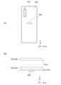
- FIG. 1 schematically shows an electronic device and an electronic device cover according to an embodiment of the present disclosure.
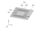
- FIG. 2 is a perspective view showing a first loop antenna and a first magnetic sheet built into an electronic device.
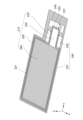
- FIG. 3 is a perspective view showing a second loop antenna and a second magnetic sheet built into the electronic device cover.
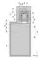
- FIG. 3 is a plan view showing a first loop antenna and a first magnetic sheet, and a second loop antenna and a second magnetic sheet when the electronic device cover is attached to the electronic device.
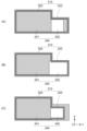
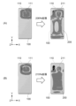
- a method of designing a second loop antenna and a second magnetic sheet is schematically shown. It is a graph showing the coupling coefficient k in different designs.
- An experimental example is schematically shown. The experimental results are schematically shown.
- An electronic device and an electronic device cover according to a first modification are schematically shown.
- An electronic device and an electronic device cover according to a second modification example are schematically shown.
- FIG. 1 schematically shows an electronic device and an electronic device cover according to an embodiment of the present disclosure.
- the electronic device 100 is, for example, a smartphone, a tablet device, a personal computer, a wearable device, or the like. Typically, electronic device 100 is larger in size than first loop antenna 110. This embodiment will be illustrated and described assuming that the electronic device 100 is a smartphone.
- the surface of the electronic device 100 that is the back surface of the touch panel surface 102 and includes the lens group 103 will be referred to as the main surface 101.
- the thickness direction of the electronic device 100 is the Z direction
- the short direction of the main surface 101 of the electronic device 100 is the X direction, which is one direction perpendicular to the Z direction
- the main surface 101 of the electronic device 100 is the Z direction and the main surface 101 of the electronic device 100, which is orthogonal to the X direction.
- the longitudinal direction is called the Y direction.
- the XY direction When the main surface direction of the electronic device 100 is intended without distinguishing between the X direction and the Y direction, it is referred to as the XY direction.
- a plane parallel to main surface 101 of electronic device 100 is referred to as an XY plane.
- the electronic device 100 includes a first loop antenna 110.
- the first loop antenna 110 is, for example, an NFC antenna, but may be an antenna of another standard.
- the electronic device 100 is larger in size and thickness than the first loop antenna 110, so the first loop antenna 110 covers only a part of the main surface 101 of the electronic device 100.
- the first loop antenna 110 is located on one side of the electronic device 100 in the X direction and one side in the Y direction, and is located not on the touch panel surface 102 side but on the main surface 101 side in the Z direction.
- the communication range 111 of the first loop antenna 110 in the XY directions is limited to the area around the first loop antenna 110, and the communication range in the Z direction is stronger on the main surface 101 side than on the touch panel surface 102 side. Therefore, the user needs to hold up a portion of the main surface 101 of the electronic device 100 corresponding to the communication range 111 over a reader/writer terminal or the like. However, the user may not know which part of the electronic device 100 corresponds to the communication range 111, or even if the user knows, the user may not be able to hold the electronic device 100 over the part corresponding to the communication range 111 due to the way the user holds the electronic device 100. be.
- the electronic device cover 200 can be attached to the main surface 101 of the electronic device 100 in the Z direction.
- the electronic device cover 200 has a second loop antenna 210 built therein.
- the second loop antenna 210 is larger in the XY directions than the first loop antenna 110, and has a shape that spreads over the entire main surface 101 of the electronic device 100 when the electronic device cover 200 is attached to the electronic device 100. has.
- the material and coating agent of the electronic device cover 200 can minimize the influence on the sensitivity of the first loop antenna 110 and the second loop antenna 210 and the accuracy of the compass built into the electronic device 100. Something is desirable.
- the material of the electronic device cover 200 may be, for example, polycarbonate, thermoplastic polyurethane (TPU), silicone, wood, synthetic leather, natural leather, cloth, or the like.
- FIG. 2 is a perspective view showing a first loop antenna and a first magnetic sheet built into an electronic device.
- the electronic device 100 has a first loop antenna 110.
- Electronic device 100 may further include first magnetic sheet 140.
- electronic device 100 includes a first loop antenna 110 and a first magnetic sheet 140.
- the first loop antenna 110 operates using power supplied from a battery (not shown) of the electronic device 100.
- the first loop antenna 110 has a first loop portion 120 and a first magnetic flux penetration region 130.
- the first loop antenna 110 is formed, for example, on a polyimide sheet (not shown).
- the first loop portion 120 is typically made of copper and is a single loop coil wound on the XY plane.
- the specifications of the first loop portion 120 are, for example, 4 turns (4 turns), a coil width of 1 mm, and a space between the coils of 1 mm.
- the first magnetic flux penetration region 130 is a region on the XY plane defined by the innermost line 121 of the first loop portion 120, and is provided inside the first loop portion 120 to allow magnetic flux to penetrate in the Z direction.
- the first magnetic sheet 140 is stacked on the first loop portion 120 and the first magnetic flux penetration region 130 of the first loop antenna 110 so as to face each other in the Z direction.
- the first magnetic sheet 140 is typically made of ferrite and has magnetism. The first magnetic sheet 140 prevents cancellation of the magnetic flux generated in the first loop antenna 110 and stabilizes the magnetic flux.
- FIG. 3 is a perspective view showing the second loop antenna and second magnetic sheet built into the electronic device cover.
- the electronic device cover 200 includes a second loop antenna 210, a capacitor module 270 (FIG. 1), and a second magnetic sheet 240.
- the second loop antenna 210 is connected to the capacitor module 270 (FIG. 1) and operates with the induced power of the first loop antenna 110. Conversely, the electronic device cover 200 does not have a battery that supplies power to the second loop antenna 210.
- the second loop antenna 210 has a second loop portion 220 and a third loop portion 250, and a second magnetic flux penetration region 230 and a third magnetic flux penetration region 260.
- the second loop antenna 210 is formed, for example, on a polyimide sheet (not shown).
- the second loop section 220 and the third loop section 250 are typically made of copper and are one continuous loop coil wound on the XY plane.
- the specifications of the second loop part 220 and the third loop part 250 are, for example, two turns (two turns), a coil width of 1 mm, and a space between the coils of 1 mm.
- the second loop portion 220 When the electronic device cover 200 is attached to the electronic device 100, the second loop portion 220 has at least a portion facing the first loop portion 120 of the first loop antenna 110 in the Z direction, and It is magnetically coupled to the loop antenna 110 of No. 1.
- the second magnetic flux penetration region 230 is a region on the XY plane defined by the innermost line 221 of the second loop portion 220, is provided inside the second loop portion 220, and allows magnetic flux to penetrate in the Z direction. .
- the third loop portion 250 faces the first loop portion 120 of the first loop antenna 110 and the first magnetic flux penetration region 130 in the Z direction when the electronic device cover 200 is attached to the electronic device 100. Instead, it spreads in the XY directions of the electronic device 100 that are perpendicular to the Z direction.
- the third magnetic flux penetration region 260 is a region on the XY plane divided by the innermost line 251 of the third loop portion 250, is provided inside the third loop portion 250, and allows magnetic flux to penetrate in the Z direction. .
- the second magnetic sheet 240 is stacked on the second loop antenna 210 so as to face it in the Z direction.
- the second magnetic sheet 240 is typically made of ferrite.
- the second magnetic sheet 240 has a magnetic part 241 and a non-magnetic part 242.
- the magnetic part 241 has magnetism and faces the third loop part 250 and the third magnetic flux penetration region 260 in the Z direction.
- the magnetic part 241 prevents cancellation of the magnetic flux generated in the third loop part 250 and stabilizes the magnetic flux.
- the non-magnetic portion 242 is a region obtained by cutting out the second magnetic sheet 240, that is, an air layer. Therefore, the second magnetic sheet 240 including the non-magnetic portion 242 can be manufactured easily and inexpensively, and the weight can be reduced.
- the non-magnetic portion 242 has no magnetism and faces the second loop portion 220 and the second magnetic flux penetration region 230 in the Z direction. Conversely, the second loop portion 220 and the second magnetic flux penetration region 230 do not face the magnetic portion 241 in the Z direction.
- the boundary 243 of the non-magnetic portion 242 and the outermost line 222 of the second loop portion 220 are spaced apart in the XY direction.
- the distance D1 in the X direction and the Y direction between the boundary 243 of the non-magnetic part 242 and the outermost line 222 of the second loop part 220 is, for example, 9 mm ⁇ D1 ⁇ 10 mm, respectively.
- FIG. 4 is a plan view showing the first loop antenna and first magnetic sheet, and the second loop antenna and second magnetic sheet when the electronic device cover is attached to the electronic device.
- the second loop portion 220 of the second loop antenna 210 faces the first loop antenna 110 in the Z direction
- the third loop portion 220 of the second loop antenna 210 faces the first loop antenna 110 in the Z direction.
- the loop portion 250 does not face the first loop antenna 110 in the Z direction but extends in the XY directions.
- the distance D4 (FIG. 1) between the first loop antenna 110 and the second loop antenna 210 in the Z direction is, for example, 0.89 mm.
- the innermost line 121 of the first loop portion 120 faces at least a portion of the second loop portion 220 in the Z direction, and the second loop portion 220
- the innermost line 221 faces the first magnetic flux penetration region 130 in the Z direction. That is, the innermost line 121 of the first loop part 120 and the innermost line 221 of the second loop part 220 are not opposed to each other in the Z direction, but the innermost line 221 of the second loop part 220 is opposite to the innermost line 221 of the second loop part 220. It is arranged inside the innermost line 121 of the loop portion 120 (on the side of the first magnetic flux penetrating region 130 and the second magnetic flux penetrating region 230).
- the amount of deviation D2 between the innermost line 121 of the first loop part 120 and the innermost line 221 of the second loop part 220 in the X direction and the Y direction is, for example, 0.5 mm, respectively.
- the boundary of the non-magnetic portion 242 and the outermost line 112 of the first loop portion 120 are separated in the XY direction.
- the distance D3 between the boundary 243 of the non-magnetic portion 242 and the outermost line 122 of the first loop portion 120 in the X direction and the Y direction is, for example, 4 mm, respectively.
- the outer portion of the first magnetic sheet 140 faces the magnetic portion 241 of the second magnetic sheet 240 in the Z direction.
- the second loop portions 220 of the first loop antenna 110 and the second loop antenna 210 are both attached to the non-magnetic portion 242 of the second magnetic sheet 240. They face each other in the Z direction and do not face the magnetic part 241. Therefore, when the electronic device cover 200 is attached to the electronic device 100, the non-magnetic portion 242 faces the first loop portion 120 and the first magnetic flux penetration region 130 in the Z direction, and directs the magnetic flux in the Z direction. penetrate.
- the magnetic flux of the first loop antenna 110 and the magnetic flux of the second loop portion 220 of the second loop antenna 210 are magnetically coupled via the non-magnetic portion 242 of the second magnetic sheet 240. Thereby, it is possible to increase the magnetic coupling between the magnetic fluxes of the first loop antenna 110 and the second loop antenna 210 in the Z direction, and to expand the communication range of the main surface 101 and the touch panel surface 102 in the Z direction.
- the third loop part 250 of the second loop antenna 210 faces the non-magnetic part 241 of the second magnetic sheet 240 in the Z direction, cancellation of the magnetic flux generated in the third loop part 250 can be prevented.
- the magnetic flux becomes stable. Thereby, the communication range 211 of the first loop antenna 110 in the X and Y directions can be stably expanded.
- FIG. 5 schematically shows a method of designing the second loop antenna and the second magnetic sheet.
- the second loop antenna 210 and the second magnetic sheet 240 are designed for each model based on the first loop antenna 110 and the first magnetic sheet 140 of the electronic device 100.
- the second loop antenna 210 and the second magnetic sheet 240 are constructed using a coupling coefficient calculation model so that the magnetic coupling coefficient k between the first loop antenna 110 and the second loop antenna 210 is high. It is desirable to perform a simulation before designing. An example of the design method will be described below.
- the shapes of the second loop antenna 210 and the second magnetic sheet 240 are made to follow the outline of the main surface 101 of the electronic device 100 excluding the lens group 103.
- the shape and size of the non-magnetic portion 242 of the second magnetic sheet 240 are the same as the shape and size of the first magnetic sheet 140, and the non-magnetic portion 242 and the first magnetic sheet 140 are arranged to face each other in the Z direction. Make it.
- the design of the second loop antenna 210 is not changed, and the non-magnetic part 242 is enlarged so that the second loop antenna 210 faces the non-magnetic part 242 in the Z direction. Make it.
- the configuration (B) has a better coupling coefficient than the configuration (A).
- the shape and size of the non-magnetic part 242 of the second magnetic sheet 240 are changed, the shape of the second loop part 220 of the second loop antenna 210 is changed, and the first loop A design that increases the magnetic coupling coefficient k between the antenna 110 and the second loop antenna 210 may be determined.
- FIG. 6 is a graph showing the coupling coefficient k in different designs.
- Boxsize means a change from the considered standard shape of the non-magnetic portion 242. Therefore, if the shape of the non-magnetic portion 242 is set to ⁇ 0.5 mm from the size used as the standard for consideration, the coupling coefficient k between the first loop antenna 110 and the second loop antenna 210 can be increased.
- Headsize means a change from the considered reference line length of the second loop portion 220. Therefore, when the short side line length of the second loop portion 220 is set to 7.0 mm, the coupling coefficient k between the first loop antenna 110 and the second loop antenna 210 can be increased.
- FIG. 7 schematically shows an experimental example.
- An electronic device 100 with a main surface 101 of 68 mm x 158 mm was prepared.
- An electronic device cover 200 incorporating a second loop antenna 210 and a second magnetic sheet 240 designed to be suitable for the electronic device 100 was prepared.
- An NFC tag 300 with a size of 26 mm x 9.5 mm and a communication distance of 10 mm was prepared.
- the center in the XY direction of the main surface 101 of the electronic device 100 without the electronic device cover 200 attached was brought close to the NFC tag 300.
- the distance in the Z direction between the main surface 101 and the NFC tag 300 was set to 1 mm, and the area of the communication range 111 in the XY directions was measured.
- the center in the XY direction of the main surface 101 of the electronic device 100 with the electronic device cover 200 attached was brought close to the NFC tag 300.
- the distance in the Z direction between the main surface 101 and the NFC tag 300 was set to 1 mm, and the area of the communication range 211 in the XY directions was measured.
- FIG. 8 schematically shows the experimental results.
- the communication range 111 in the XY directions of the first comparative example is 100%
- the communication range 211 in the XY directions of the first example has expanded to 206%.
- the center of the main surface 101 of the electronic device 100 without the electronic device cover 200 attached in the XY direction is brought close to the NFC tag 300, and the distance between the main surface 101 and the NFC tag 300 in the Z direction is 7 mm.
- the area of the communication range 111 in the XY directions was measured.
- the center of the main surface 101 of the electronic device 100 with the electronic device cover 200 attached thereto in the XY direction was brought close to the NFC tag 300.
- the distance in the Z direction between the main surface 101 and the NFC tag 300 was set to 7 mm, and the area of the communication range 211 in the XY directions was measured.
- the communication range 111 in the XY directions of the first comparative example is 100%
- the communication range 211 in the XY directions of the first example has been expanded to 215%.
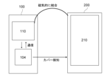
- FIG. 9 schematically shows an electronic device and an electronic device cover according to a first modification.
- the electronic device 100 further includes a first control circuit 104.
- the first control circuit 104 detects whether the electronic device cover 200 is attached to the electronic device 100 or not. "The electronic device cover 200 is not attached" means that no cover is attached to the electronic device 100, or that a cover other than the electronic device cover 200 of this embodiment is attached.
- the first control circuit 104 stores the resonant frequencies of the first loop antenna 110 and the second loop antenna 210 when the electronic device cover 200 of this embodiment is attached to the electronic device 100, If a resonance frequency matching that value is detected, it may be determined that the electronic device cover 200 is attached to the electronic device 100.
- the second loop antenna 210 operates using the induced power of the first loop antenna 110. Therefore, the first control circuit 104 controls the power applied to the first loop antenna 110 when the electronic device cover 200 is attached to the electronic device 100, and the power applied to the first loop antenna 110 when the electronic device cover 200 is attached to the electronic device 100.
- the power is set higher than the power (standard value) applied to the first loop antenna 110 when the antenna is not in use. Thereby, the induced power obtained by the second loop antenna 210 can be increased.
- the power applied to the first loop antenna 110 can be suppressed, contributing to power saving.
- FIG. 10 schematically shows an electronic device and an electronic device cover according to a second modification.
- the electronic device cover 200 includes a second control circuit 204 and a plurality of capacitors 271, 272, 273 as a capacitor module 270.
- the plurality of capacitors 271, 272, and 273 are connected in parallel to the second loop antenna 210, and have at least some different capacitances. Typically, the capacitances of the plurality of capacitors 271, 272, 273 are all different. For example, the plurality of capacitors 271, 272, and 273 have different capacitance multipliers.
- the second control circuit 204 detects the frequency of the first loop antenna 110 when the electronic device cover 200 is attached to the electronic device 100, and selects one or more capacitors 271, 272 and/or 273 based on the frequency. to dynamically control the power applied to the second loop antenna 210.
- the second control circuit 204 selectively turns on and off one or more capacitors 271, 272, and/or 273 according to individual differences in the electronic device 100, and optimizes the capacitor value. Since the power applied to the second loop antenna 210 is dynamically changed according to individual differences in the electronic device 100, it is possible to prevent unnecessarily large power from being applied to the second loop antenna 210, contributing to power saving. do.
- the first modified example and the second modified example are not alternative and may be combined. This allows one type of electronic device cover 200 to optimize power for a plurality of different types of electronic devices 100.
- the first control circuit 104 of the electronic device 100 detects the frequency of the first loop antenna 110 and transmits the frequency to the second control circuit 204 of the electronic device cover 200.
- the one or more capacitors 271, 272 and/or 273 may be selectively switched based on the frequency received by the second control circuit 204.
- the second loop antenna 210 and the second magnetic sheet 240 may be built into the main body of the electronic device 100 instead of being provided in the electronic device cover 200 that can be attached to the main body of the electronic device 100 as in the above embodiment. good.
- the second loop antenna 210 and the second magnetic sheet 240 may be arranged on the touch panel surface 102 side of the electronic device 100.
- the electronic device cover 200 is a notebook type cover that covers the main surface 101 and the touch panel surface 102, only the main surface 101 side of the electronic device cover 200, only the touch panel surface 102 side of the electronic device cover 200, or the electronic device cover
- the second loop antenna 210 and the second magnetic sheet 240 may be arranged on both the main surface 101 side and the touch panel surface 102 side of the antenna 200 .
- the magnetic flux of the first loop antenna 110 and the magnetic flux of the second loop portion 220 of the second loop antenna 210 are magnetically coupled via the non-magnetic portion 242 of the second magnetic sheet 240. Thereby, it is possible to increase the magnetic coupling between the magnetic fluxes of the first loop antenna 110 and the second loop antenna 210 in the Z direction, and to expand the communication range of the main surface 101 and the touch panel surface 102 in the Z direction.
- the third loop part 250 of the second loop antenna 210 faces the non-magnetic part 241 of the second magnetic sheet 240 in the Z direction, cancellation of the magnetic flux generated in the third loop part 250 can be prevented.
- the magnetic flux becomes stable. Thereby, the communication range 211 of the first loop antenna 110 in the X and Y directions can be stably expanded.
- the second loop antenna 210 operates using the induced power of the first loop antenna 110 and does not require a battery to supply power to the second loop antenna 210, which contributes to reducing the weight of the electronic device cover 200. do.
- the present disclosure may have the following configurations.
- the electronic device has a first loop antenna having a first loop portion and a first magnetic flux penetration region that is provided inside the first loop portion and allows magnetic flux to penetrate in the thickness direction of the electronic device.
- a second loop portion at least a portion of which faces the first loop portion in the thickness direction and magnetically couples with the first loop antenna; a second magnetic flux penetration region that is provided inside the second loop portion and allows the magnetic flux to penetrate in the thickness direction;
- a direction of the main surface of the electronic device that is continuous with the second loop portion, does not face the first loop portion and the first magnetic flux penetration region in the thickness direction, and is perpendicular to the thickness direction.
- An electronic device cover comprising: a second loop antenna; (2) The electronic device cover according to (1) above, a magnetic part that has magnetism and faces the third loop part in the thickness direction;
- the first loop has no magnetism, faces the second loop portion and the second magnetic flux penetration region in the thickness direction, and when the electronic device cover is attached to the electronic device, the first loop and a non-magnetic portion that faces the first magnetic flux penetrating region in the thickness direction and allows the magnetic flux to penetrate in the thickness direction;
- the magnetic sheet may further include a magnetic sheet having the following.
- the non-magnetic portion may be a region obtained by cutting out the magnetic sheet.
- the innermost line of the first loop portion may face at least a portion of the second loop portion in the thickness direction.
- the innermost line of the second loop portion may face the first magnetic flux penetration region in the thickness direction.
- the electronic device cover according to any one of (1) to (5) above The boundary of the non-magnetic part and the outermost line of the second loop part are spaced apart in the direction of the main surface, When the electronic device cover is attached to the electronic device, a boundary of the non-magnetic portion and an outermost line of the first loop antenna may be separated from each other in the direction of the main surface.
- the second loop antenna operates with the induced power of the first loop antenna, The electronic device may apply power to the first loop antenna when the electronic device cover is attached to the electronic device, and apply power to the first loop antenna when the electronic device cover is not attached to the electronic device.
- the antenna may further include a first control circuit that applies a power higher than the power applied to the loop antenna.
- a first control circuit that applies a power higher than the power applied to the loop antenna.
- the electronic device cover according to any one of (1) to (7) above, a plurality of capacitors connected in parallel to the second loop antenna, at least some of which have different capacitances; When the electronic device cover is attached to the electronic device, power is applied to the second loop antenna by detecting the frequency of the first loop antenna and selectively switching one or more capacitors based on the frequency.
- a second control circuit that controls the You may further comprise.
- the first loop antenna may be an NFC antenna.
- a first loop antenna having a first loop portion and a first magnetic flux penetration region provided inside the first loop portion and allowing magnetic flux to penetrate in the thickness direction of the electronic device; a second loop portion at least a portion of which faces the first loop portion in the thickness direction and magnetically couples with the first loop antenna; a second magnetic flux penetration region that is provided inside the second loop portion and allows the magnetic flux to penetrate in the thickness direction; A direction of the main surface of the electronic device that is continuous with the second loop portion, does not face the first loop portion and the first magnetic flux penetration region in the thickness direction, and is perpendicular to the thickness direction.
- a second loop portion When installed, a second loop portion at least a portion of which faces the first loop portion in the thickness direction and magnetically couples with the first loop antenna; a second magnetic flux penetration region that is provided inside the second loop portion and allows the magnetic flux to penetrate in the thickness direction; A direction of the main surface of the electronic device that is continuous with the second loop portion, does not face the first loop portion and the first magnetic flux penetration region in the thickness direction, and is perpendicular to the thickness direction.
- the second loop antenna operates with the induced power of the first loop antenna, The power applied to the first loop antenna when the electronic device cover is attached to the electronic device is applied to the first loop antenna when the electronic device cover is not attached to the electronic device.
- control method (15) The control method according to (13) or (14) above, The electronic device cover further includes a plurality of capacitors connected in parallel to the second loop antenna, at least some of which have different capacitances, When the electronic device cover is attached to the electronic device, the frequency of the first loop antenna is detected, and one or more capacitors are turned on based on the frequency to control the power applied to the second loop antenna. Control method.
- Second control circuit 110 First loop antenna 111 Communication range 112 Outermost line 120 First loop part 121 Innermost line 122 Outermost line 130 First magnetic flux penetration area 140 First magnetic sheet 200 Electronic equipment cover 204 Second control circuit 210 Second loop antenna 211 Communication range 220 Second loop section 221 Innermost line 222 Outermost line 230 Second magnetic flux penetration area 240 Second magnetic sheet 241 Magnetic part 242 Magnetic part 243 Boundary 250 Third loop part 251 Innermost line 260 Third magnetic flux penetration region 270 Capacitor module
Landscapes
- Engineering & Computer Science (AREA)
- Computer Hardware Design (AREA)
- Microelectronics & Electronic Packaging (AREA)
- Physics & Mathematics (AREA)
- General Physics & Mathematics (AREA)
- Theoretical Computer Science (AREA)
- Support Of Aerials (AREA)
Priority Applications (1)
| Application Number | Priority Date | Filing Date | Title |
|---|---|---|---|
| JP2024514820A JPWO2023199596A1 (cg-RX-API-DMAC7.html) | 2022-04-15 | 2023-02-17 |
Applications Claiming Priority (2)
| Application Number | Priority Date | Filing Date | Title |
|---|---|---|---|
| JP2022-067341 | 2022-04-15 | ||
| JP2022067341 | 2022-04-15 |
Publications (1)
| Publication Number | Publication Date |
|---|---|
| WO2023199596A1 true WO2023199596A1 (ja) | 2023-10-19 |
Family
ID=88329562
Family Applications (1)
| Application Number | Title | Priority Date | Filing Date |
|---|---|---|---|
| PCT/JP2023/005647 Ceased WO2023199596A1 (ja) | 2022-04-15 | 2023-02-17 | 電子機器カバー、電子機器及び制御方法 |
Country Status (2)
| Country | Link |
|---|---|
| JP (1) | JPWO2023199596A1 (cg-RX-API-DMAC7.html) |
| WO (1) | WO2023199596A1 (cg-RX-API-DMAC7.html) |
Citations (1)
| Publication number | Priority date | Publication date | Assignee | Title |
|---|---|---|---|---|
| JP2008167144A (ja) * | 2006-12-28 | 2008-07-17 | Nec Tokin Corp | アンテナ装置 |
Family Cites Families (4)
| Publication number | Priority date | Publication date | Assignee | Title |
|---|---|---|---|---|
| JPH10293828A (ja) * | 1997-04-18 | 1998-11-04 | Omron Corp | データキャリア、コイルモジュール、リーダライタ及び衣服データ取得方法 |
| JP2006048580A (ja) * | 2004-08-09 | 2006-02-16 | Olympus Corp | 情報端末装置 |
| JP4639857B2 (ja) * | 2005-03-07 | 2011-02-23 | 富士ゼロックス株式会社 | Rfidタグが取り付けられた物品を収納する収納箱、その配置方法、通信方法、通信確認方法および包装構造。 |
| JP6102239B2 (ja) * | 2012-12-17 | 2017-03-29 | 大日本印刷株式会社 | ループアンテナ中継装置、通信システム |
-
2023
- 2023-02-17 WO PCT/JP2023/005647 patent/WO2023199596A1/ja not_active Ceased
- 2023-02-17 JP JP2024514820A patent/JPWO2023199596A1/ja active Pending
Patent Citations (1)
| Publication number | Priority date | Publication date | Assignee | Title |
|---|---|---|---|---|
| JP2008167144A (ja) * | 2006-12-28 | 2008-07-17 | Nec Tokin Corp | アンテナ装置 |
Also Published As
| Publication number | Publication date |
|---|---|
| JPWO2023199596A1 (cg-RX-API-DMAC7.html) | 2023-10-19 |
Similar Documents
| Publication | Publication Date | Title |
|---|---|---|
| KR101318707B1 (ko) | 안테나 장치 및 이동체 통신 단말 | |
| US10403979B2 (en) | Antenna apparatus and electronic device including the same | |
| US10020673B2 (en) | Electronic device including non-contact charging module and battery | |
| JP4174801B2 (ja) | 識別タグのリーダライタ用アンテナ | |
| KR101664970B1 (ko) | 코일 안테나 및 비접촉 정보매체 | |
| CN101213567B (zh) | 基板安装用天线线圈及天线装置 | |
| JP4893631B2 (ja) | アンテナ装置 | |
| US20140145906A1 (en) | Antenna device and wireless communication device | |
| CN112018498B (zh) | 天线装置以及具备其的ic卡 | |
| US20140218262A1 (en) | Antenna device and wireless communication apparatus | |
| EP1713145A1 (en) | Small loop antenna for induction reader/writer | |
| US10122418B2 (en) | Coupling assistance device and RFID communication system | |
| WO2004029868A1 (ja) | アンテナ装置及びアンテナ装置を用いた通信装置 | |
| JP2007043535A (ja) | Rf−idリーダーライター装置用アンテナ及びそれを用いたrf−idリーダーライター装置並びにrf−idシステム | |
| US10164347B2 (en) | Antenna device and electronic appliance | |
| US8770489B2 (en) | Radio communication device | |
| US8730120B2 (en) | Transmission/reception antenna and transmission/reception device using same | |
| JP2013138404A (ja) | 伝送コイル及び携帯無線端末 | |
| CN205621840U (zh) | 天线装置 | |
| JP6590119B1 (ja) | Rfidタグ及びrfid付き物品 | |
| JP2004206479A (ja) | 非接触タグ | |
| JP2017153060A (ja) | アンテナ装置および電子機器 | |
| WO2014058072A1 (ja) | Hf帯無線通信デバイス | |
| US20190148815A1 (en) | Antenna module and radio equipment | |
| JP2007214646A (ja) | 非接触通信用アンテナ |
Legal Events
| Date | Code | Title | Description |
|---|---|---|---|
| 121 | Ep: the epo has been informed by wipo that ep was designated in this application |
Ref document number: 23788019 Country of ref document: EP Kind code of ref document: A1 |
|
| WWE | Wipo information: entry into national phase |
Ref document number: 2024514820 Country of ref document: JP |
|
| NENP | Non-entry into the national phase |
Ref country code: DE |
|
| 122 | Ep: pct application non-entry in european phase |
Ref document number: 23788019 Country of ref document: EP Kind code of ref document: A1 |