WO2023190800A1 - 感光性樹脂フィルム、プリント配線板、半導体パッケージ及びプリント配線板の製造方法 - Google Patents
感光性樹脂フィルム、プリント配線板、半導体パッケージ及びプリント配線板の製造方法 Download PDFInfo
- Publication number
- WO2023190800A1 WO2023190800A1 PCT/JP2023/013043 JP2023013043W WO2023190800A1 WO 2023190800 A1 WO2023190800 A1 WO 2023190800A1 JP 2023013043 W JP2023013043 W JP 2023013043W WO 2023190800 A1 WO2023190800 A1 WO 2023190800A1
- Authority
- WO
- WIPO (PCT)
- Prior art keywords
- photosensitive resin
- resin film
- component
- resin
- mass
- Prior art date
- Legal status (The legal status is an assumption and is not a legal conclusion. Google has not performed a legal analysis and makes no representation as to the accuracy of the status listed.)
- Ceased
Links
Images
Classifications
-
- G—PHYSICS
- G03—PHOTOGRAPHY; CINEMATOGRAPHY; ANALOGOUS TECHNIQUES USING WAVES OTHER THAN OPTICAL WAVES; ELECTROGRAPHY; HOLOGRAPHY
- G03F—PHOTOMECHANICAL PRODUCTION OF TEXTURED OR PATTERNED SURFACES, e.g. FOR PRINTING, FOR PROCESSING OF SEMICONDUCTOR DEVICES; MATERIALS THEREFOR; ORIGINALS THEREFOR; APPARATUS SPECIALLY ADAPTED THEREFOR
- G03F7/00—Photomechanical, e.g. photolithographic, production of textured or patterned surfaces, e.g. printing surfaces; Materials therefor, e.g. comprising photoresists; Apparatus specially adapted therefor
- G03F7/004—Photosensitive materials
- G03F7/027—Non-macromolecular photopolymerisable compounds having carbon-to-carbon double bonds, e.g. ethylenic compounds
- G03F7/028—Non-macromolecular photopolymerisable compounds having carbon-to-carbon double bonds, e.g. ethylenic compounds with photosensitivity-increasing substances, e.g. photoinitiators
-
- G—PHYSICS
- G03—PHOTOGRAPHY; CINEMATOGRAPHY; ANALOGOUS TECHNIQUES USING WAVES OTHER THAN OPTICAL WAVES; ELECTROGRAPHY; HOLOGRAPHY
- G03F—PHOTOMECHANICAL PRODUCTION OF TEXTURED OR PATTERNED SURFACES, e.g. FOR PRINTING, FOR PROCESSING OF SEMICONDUCTOR DEVICES; MATERIALS THEREFOR; ORIGINALS THEREFOR; APPARATUS SPECIALLY ADAPTED THEREFOR
- G03F7/00—Photomechanical, e.g. photolithographic, production of textured or patterned surfaces, e.g. printing surfaces; Materials therefor, e.g. comprising photoresists; Apparatus specially adapted therefor
- G03F7/004—Photosensitive materials
-
- G—PHYSICS
- G03—PHOTOGRAPHY; CINEMATOGRAPHY; ANALOGOUS TECHNIQUES USING WAVES OTHER THAN OPTICAL WAVES; ELECTROGRAPHY; HOLOGRAPHY
- G03F—PHOTOMECHANICAL PRODUCTION OF TEXTURED OR PATTERNED SURFACES, e.g. FOR PRINTING, FOR PROCESSING OF SEMICONDUCTOR DEVICES; MATERIALS THEREFOR; ORIGINALS THEREFOR; APPARATUS SPECIALLY ADAPTED THEREFOR
- G03F7/00—Photomechanical, e.g. photolithographic, production of textured or patterned surfaces, e.g. printing surfaces; Materials therefor, e.g. comprising photoresists; Apparatus specially adapted therefor
- G03F7/004—Photosensitive materials
- G03F7/0042—Photosensitive materials with inorganic or organometallic light-sensitive compounds not otherwise provided for, e.g. inorganic resists
- G03F7/0043—Chalcogenides; Silicon, germanium, arsenic or derivatives thereof; Metals, oxides or alloys thereof
-
- G—PHYSICS
- G03—PHOTOGRAPHY; CINEMATOGRAPHY; ANALOGOUS TECHNIQUES USING WAVES OTHER THAN OPTICAL WAVES; ELECTROGRAPHY; HOLOGRAPHY
- G03F—PHOTOMECHANICAL PRODUCTION OF TEXTURED OR PATTERNED SURFACES, e.g. FOR PRINTING, FOR PROCESSING OF SEMICONDUCTOR DEVICES; MATERIALS THEREFOR; ORIGINALS THEREFOR; APPARATUS SPECIALLY ADAPTED THEREFOR
- G03F7/00—Photomechanical, e.g. photolithographic, production of textured or patterned surfaces, e.g. printing surfaces; Materials therefor, e.g. comprising photoresists; Apparatus specially adapted therefor
- G03F7/004—Photosensitive materials
- G03F7/0046—Photosensitive materials with perfluoro compounds, e.g. for dry lithography
-
- G—PHYSICS
- G03—PHOTOGRAPHY; CINEMATOGRAPHY; ANALOGOUS TECHNIQUES USING WAVES OTHER THAN OPTICAL WAVES; ELECTROGRAPHY; HOLOGRAPHY
- G03F—PHOTOMECHANICAL PRODUCTION OF TEXTURED OR PATTERNED SURFACES, e.g. FOR PRINTING, FOR PROCESSING OF SEMICONDUCTOR DEVICES; MATERIALS THEREFOR; ORIGINALS THEREFOR; APPARATUS SPECIALLY ADAPTED THEREFOR
- G03F7/00—Photomechanical, e.g. photolithographic, production of textured or patterned surfaces, e.g. printing surfaces; Materials therefor, e.g. comprising photoresists; Apparatus specially adapted therefor
- G03F7/004—Photosensitive materials
- G03F7/027—Non-macromolecular photopolymerisable compounds having carbon-to-carbon double bonds, e.g. ethylenic compounds
-
- G—PHYSICS
- G03—PHOTOGRAPHY; CINEMATOGRAPHY; ANALOGOUS TECHNIQUES USING WAVES OTHER THAN OPTICAL WAVES; ELECTROGRAPHY; HOLOGRAPHY
- G03F—PHOTOMECHANICAL PRODUCTION OF TEXTURED OR PATTERNED SURFACES, e.g. FOR PRINTING, FOR PROCESSING OF SEMICONDUCTOR DEVICES; MATERIALS THEREFOR; ORIGINALS THEREFOR; APPARATUS SPECIALLY ADAPTED THEREFOR
- G03F7/00—Photomechanical, e.g. photolithographic, production of textured or patterned surfaces, e.g. printing surfaces; Materials therefor, e.g. comprising photoresists; Apparatus specially adapted therefor
- G03F7/004—Photosensitive materials
- G03F7/027—Non-macromolecular photopolymerisable compounds having carbon-to-carbon double bonds, e.g. ethylenic compounds
- G03F7/032—Non-macromolecular photopolymerisable compounds having carbon-to-carbon double bonds, e.g. ethylenic compounds with binders
-
- G—PHYSICS
- G03—PHOTOGRAPHY; CINEMATOGRAPHY; ANALOGOUS TECHNIQUES USING WAVES OTHER THAN OPTICAL WAVES; ELECTROGRAPHY; HOLOGRAPHY
- G03F—PHOTOMECHANICAL PRODUCTION OF TEXTURED OR PATTERNED SURFACES, e.g. FOR PRINTING, FOR PROCESSING OF SEMICONDUCTOR DEVICES; MATERIALS THEREFOR; ORIGINALS THEREFOR; APPARATUS SPECIALLY ADAPTED THEREFOR
- G03F7/00—Photomechanical, e.g. photolithographic, production of textured or patterned surfaces, e.g. printing surfaces; Materials therefor, e.g. comprising photoresists; Apparatus specially adapted therefor
- G03F7/004—Photosensitive materials
- G03F7/027—Non-macromolecular photopolymerisable compounds having carbon-to-carbon double bonds, e.g. ethylenic compounds
- G03F7/032—Non-macromolecular photopolymerisable compounds having carbon-to-carbon double bonds, e.g. ethylenic compounds with binders
- G03F7/033—Non-macromolecular photopolymerisable compounds having carbon-to-carbon double bonds, e.g. ethylenic compounds with binders the binders being polymers obtained by reactions only involving carbon-to-carbon unsaturated bonds, e.g. vinyl polymers
-
- G—PHYSICS
- G03—PHOTOGRAPHY; CINEMATOGRAPHY; ANALOGOUS TECHNIQUES USING WAVES OTHER THAN OPTICAL WAVES; ELECTROGRAPHY; HOLOGRAPHY
- G03F—PHOTOMECHANICAL PRODUCTION OF TEXTURED OR PATTERNED SURFACES, e.g. FOR PRINTING, FOR PROCESSING OF SEMICONDUCTOR DEVICES; MATERIALS THEREFOR; ORIGINALS THEREFOR; APPARATUS SPECIALLY ADAPTED THEREFOR
- G03F7/00—Photomechanical, e.g. photolithographic, production of textured or patterned surfaces, e.g. printing surfaces; Materials therefor, e.g. comprising photoresists; Apparatus specially adapted therefor
- G03F7/004—Photosensitive materials
- G03F7/038—Macromolecular compounds which are rendered insoluble or differentially wettable
-
- G—PHYSICS
- G03—PHOTOGRAPHY; CINEMATOGRAPHY; ANALOGOUS TECHNIQUES USING WAVES OTHER THAN OPTICAL WAVES; ELECTROGRAPHY; HOLOGRAPHY
- G03F—PHOTOMECHANICAL PRODUCTION OF TEXTURED OR PATTERNED SURFACES, e.g. FOR PRINTING, FOR PROCESSING OF SEMICONDUCTOR DEVICES; MATERIALS THEREFOR; ORIGINALS THEREFOR; APPARATUS SPECIALLY ADAPTED THEREFOR
- G03F7/00—Photomechanical, e.g. photolithographic, production of textured or patterned surfaces, e.g. printing surfaces; Materials therefor, e.g. comprising photoresists; Apparatus specially adapted therefor
- G03F7/004—Photosensitive materials
- G03F7/09—Photosensitive materials characterised by structural details, e.g. supports, auxiliary layers
- G03F7/095—Photosensitive materials characterised by structural details, e.g. supports, auxiliary layers having more than one photosensitive layer
-
- H—ELECTRICITY
- H05—ELECTRIC TECHNIQUES NOT OTHERWISE PROVIDED FOR
- H05K—PRINTED CIRCUITS; CASINGS OR CONSTRUCTIONAL DETAILS OF ELECTRIC APPARATUS; MANUFACTURE OF ASSEMBLAGES OF ELECTRICAL COMPONENTS
- H05K1/00—Printed circuits
- H05K1/02—Details
- H05K1/03—Use of materials for the substrate
-
- H—ELECTRICITY
- H05—ELECTRIC TECHNIQUES NOT OTHERWISE PROVIDED FOR
- H05K—PRINTED CIRCUITS; CASINGS OR CONSTRUCTIONAL DETAILS OF ELECTRIC APPARATUS; MANUFACTURE OF ASSEMBLAGES OF ELECTRICAL COMPONENTS
- H05K3/00—Apparatus or processes for manufacturing printed circuits
- H05K3/46—Manufacturing multilayer circuits
-
- H—ELECTRICITY
- H10—SEMICONDUCTOR DEVICES; ELECTRIC SOLID-STATE DEVICES NOT OTHERWISE PROVIDED FOR
- H10W—GENERIC PACKAGES, INTERCONNECTIONS, CONNECTORS OR OTHER CONSTRUCTIONAL DETAILS OF DEVICES COVERED BY CLASS H10
- H10W70/00—Package substrates; Interposers; Redistribution layers [RDL]
- H10W70/01—Manufacture or treatment
- H10W70/05—Manufacture or treatment of insulating or insulated package substrates, or of interposers, or of redistribution layers
Definitions
- the present disclosure relates to a method for manufacturing a photosensitive resin film, a printed wiring board, a semiconductor package, and a printed wiring board.
- Laser processing is the mainstream method for forming vias in an interlayer insulating layer formed of a thermosetting resin film.
- reduction in the diameter of vias by laser processing is reaching its limit.
- substrate materials for printed wiring boards have dielectric properties [hereinafter sometimes referred to as "high frequency properties"] that can reduce transmission loss of high frequency signals. ], that is, a low dielectric constant and a low dielectric loss tangent are required.
- the present inventors have considered incorporating a fluorine-containing resin with a low dielectric constant into a photosensitive resin film for forming an interlayer insulating layer in order to improve the dielectric properties of the substrate material.
- a fluorine-containing resin is simply added to a photosensitive resin film, even if the dielectric constant of the interlayer insulation layer can be reduced, there is a problem in that the adhesion of the conductor, especially the adhesion strength with plated copper, decreases. occured. Therefore, it has been difficult to achieve both excellent dielectric properties and conductor adhesion.
- the present embodiment provides a photosensitive resin film capable of forming an interlayer insulating layer having excellent dielectric properties and conductor adhesion, a printed wiring board using the photosensitive resin film, a method for manufacturing the same, and a semiconductor.
- the challenge is to provide a package.
- Photosensitive resin containing (A) a compound having an ethylenically unsaturated group, (B) a thermosetting resin, (C) a photopolymerization initiator, (D) an inorganic filler, and (E) a fluorine-containing resin It is a film,
- the photosensitive resin film has a first surface and a second surface opposite to the first surface, A photosensitive resin film, wherein the fluorine atom concentration at a depth of 1 ⁇ m from the first surface is lower than the fluorine atom concentration at a depth of 1 ⁇ m from the second surface.
- a photosensitive resin film capable of forming an interlayer insulating layer having excellent dielectric properties and conductor adhesion, a printed wiring board using the photosensitive resin film, a manufacturing method thereof, and a semiconductor package are provided. I can do it.
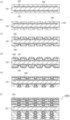
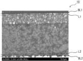
- FIG. 2 is a schematic diagram showing one aspect of the manufacturing process of a printed wiring board using the photosensitive resin film of the present embodiment as a material for an interlayer insulating layer. It is a cross-sectional SEM image for explaining the measurement position of fluorine atom concentration.
- the lower limit and upper limit of the numerical range may be replaced with the values shown in the examples. Further, the lower limit value and upper limit value of the numerical range can be arbitrarily combined with the lower limit value or upper limit value of other numerical ranges, respectively. In the notation of a numerical range "AA to BB”, the numerical values AA and BB at both ends are included in the numerical range as the lower limit value and upper limit value, respectively.
- the expression “10 or more” means 10 and a numerical value exceeding 10, and the same applies even if the numerical values are different. Further, for example, the description “10 or less” means 10 and a numerical value less than 10, and this applies even if the numerical values are different.
- the content of each component means the total content of the multiple types of substances.
- solid content means non-volatile content excluding volatile substances such as solvents. That is, “solid content” refers to components that remain without being volatilized when the resin composition is dried, and includes components that are liquid, starch syrup-like, and wax-like at room temperature. Here, in this specification, room temperature means 25°C.
- the "number of carbon atoms forming a ring” is the number of carbon atoms necessary to form a ring, and does not include the number of carbon atoms of substituents that the ring has.
- the cyclohexane skeleton and the methylcyclohexane skeleton have 6 ring carbon atoms.
- (meth)acrylic XX means one or both of acrylic XX and the corresponding methacryl XX.
- (meth)acryloyl group means one or both of an acryloyl group and a methacryloyl group.
- layer when the word "layer” is used, for example, an interlayer insulating layer, etc., it may be a solid layer, a part of the layer may be island-shaped, or a hole may be formed.
- a “layer” also includes an open embodiment and an embodiment in which the interface with an adjacent layer is unclear.
- This embodiment also includes aspects in which the items described in this specification are arbitrarily combined.
- the photosensitive resin film of this embodiment is A photosensitive resin film containing (A) a compound having an ethylenically unsaturated group, (B) a thermosetting resin, (C) a photopolymerization initiator, (D) an inorganic filler, and (E) a fluorine-containing resin.
- the photosensitive resin film has a first surface and a second surface opposite to the first surface, The fluorine atom concentration at a depth of 1 ⁇ m from the first surface is lower than the fluorine atom concentration at a depth of 1 ⁇ m from the second surface. It is a photosensitive resin film.
- each component may be abbreviated as “component (A)”, “component (B)”, etc. as appropriate.
- the fluorine atom concentration at a depth of 1 ⁇ m from the first surface is referred to as “fluorine atom concentration on the first surface”
- the fluorine atom concentration at a depth of 1 ⁇ m from the second surface is referred to as “fluorine atom concentration on the second surface”. It is sometimes abbreviated as "fluorine atomic concentration”.
- the photosensitive resin film of this embodiment can form patterns such as vias by exposure and development. Therefore, the photosensitive resin film of this embodiment is suitable for forming an interlayer insulating layer having photovias.
- photovia means a via formed by a photolithography method, that is, exposure and development.
- the overall thickness of the photosensitive resin film of this embodiment is not particularly limited, and may be, for example, 2 to 110 ⁇ m, 4 to 60 ⁇ m, or 7 to 50 ⁇ m.
- the fluorine atom concentration on the first surface is lower than the fluorine atom concentration on the second surface.
- the interlayer insulating layer obtained by curing the photosensitive resin film of this embodiment exhibits high adhesive strength with the plated copper on the first surface.
- the reason for this is presumed to be as follows. (E) Since the fluorine-containing resin has high alkali resistance, it is more difficult to dissolve than other resin components in the roughening treatment step before forming plated copper.
- the surface containing a large amount of (E) fluorine-containing resin exposed a large amount of (E) fluorine-containing resin that remained undissolved after the roughening treatment process, which was a factor in reducing the adhesion with plated copper. It will be done.
- the fluorine atom concentration on the first surface is lower than the fluorine atom concentration on the second surface, so that the first surface is exposed after the roughening treatment step (E). It is thought that the amount of fluorine-containing resin was suppressed and the adhesion to the plated copper on the surface was improved.
- the first surface of the photosensitive resin film of this embodiment is the surface on which the circuit pattern is formed by copper plating
- the second surface is the surface of the photosensitive resin film. It is preferable that it is a pasting surface when laminating.
- the fluorine atom concentrations on the first surface and the second surface are measured by the following method.
- a reference line corresponding to one surface is identified. Elemental analysis is performed on a measurement line that is 1 ⁇ m away from the reference line toward the inside of the cured product and parallel to the reference line, and the measured fluorine atom concentration on a mass basis is calculated from the fluorine atoms on one surface side. Let it be the concentration. Measure the fluorine atom concentration on the other surface side in the same way, specify the lower fluorine atom concentration as the fluorine atom concentration on the first surface, and specify the higher fluorine atom concentration on the second surface.
- Specified as fluorine atomic concentration Specified as fluorine atomic concentration.
- a cured product of the photosensitive resin film can be produced by exposure and heating.
- the fluorine atom concentration in the cured product obtained by exposing and heating the photosensitive resin film of this embodiment can be regarded as the fluorine atom concentration of the photosensitive resin film before curing.
- a more detailed method for measuring the fluorine atom concentration on the first surface and the second surface is as described in Examples.
- the fluorine atom concentration on the first surface is not particularly limited, but from the viewpoint of forming an interlayer insulating layer with better dielectric properties and conductor adhesion, it is preferably 0 to 7% by mass, more preferably 0 to 6% by mass, and more preferably 0 to 6% by mass. Preferably it is 0 to 5% by mass.
- the fluorine atom concentration on the second surface is not particularly limited as long as it is higher than the fluorine atom concentration on the first layer, but from the viewpoint of forming an interlayer insulating layer with better dielectric properties and conductor adhesion, The range higher than the concentration is preferably 8 to 60% by weight, more preferably 10 to 35% by weight, and even more preferably 15 to 30% by weight.
- the photosensitive resin film of this embodiment uses a resin composition (hereinafter referred to as "resin composition”) for forming the first surface of the photosensitive resin film in order to provide a difference in fluorine atom concentration between the first surface and the second surface. It is preferable to manufacture using a resin composition (hereinafter also referred to as “resin composition (2)”) for forming the second surface (also referred to as “resin composition (2)”).
- the resin composition (1) contains (A) a compound having an ethylenically unsaturated group, (B) a thermosetting resin, (C) a photopolymerization initiator, and (D) an inorganic filler, and the above (D) It is preferable to contain silica as the inorganic filler.
- Resin composition (2) contains (A) a compound having an ethylenically unsaturated group, (B) a thermosetting resin, (C) a photopolymerization initiator, (D) an inorganic filler, and (E) a fluorine-containing resin. It is preferable to contain. Below, each component contained in the photosensitive resin film of this embodiment will be explained, and preferred aspects of the resin composition (1) and the resin composition (2) will also be explained.
- Component (A) is not particularly limited as long as it is a compound having an ethylenically unsaturated group.
- Component (A) may be used alone or in combination of two or more.
- Component (A) is a compound that exhibits photopolymerizability, particularly radical polymerization, because it has an ethylenically unsaturated group.
- ethylenic unsaturated group means a substituent containing an ethylenically unsaturated bond.
- ethylenically unsaturated bond means a carbon-carbon double bond capable of an addition reaction, and does not include a double bond in an aromatic ring.
- Examples of the ethylenically unsaturated group include a vinyl group, an allyl group, a (meth)acryloyl group, a propargyl group, a butenyl group, an ethynyl group, a phenylethynyl group, a maleimide group, and a nadimide group.
- a (meth)acryloyl group is preferred from the viewpoint of reactivity.
- the photosensitive resin film of this embodiment preferably contains (A1) a compound having an ethylenically unsaturated group and an acidic substituent, and provides interlayer insulation with better heat resistance and dielectric properties. From the viewpoint of forming a layer, it is preferable to contain (A2) a monomer having two or more ethylenically unsaturated groups together with component (A1). Component (A1) and component (A2) will be explained below.
- component (A1) Compound having an ethylenically unsaturated group and an acidic substituent>
- the acidic substituent that component (A1) has include a carboxy group, a sulfonic acid group, and a phenolic hydroxyl group.
- a carboxy group is preferred from the viewpoint of resolution.
- the acid value of component (A1) is not particularly limited, but is preferably 20 to 200 mgKOH/g, more preferably 40 to 180 mgKOH/g, and even more preferably 70 to 150 mgKOH/g.
- the acid value of the component (A1) is at least the above lower limit, the alkali developability tends to be better.
- the acid value of the component (A1) is below the above upper limit, the dielectric constant tends to be better. Note that the acid value of component (A1) can be measured by the method described in Examples.
- the weight average molecular weight (Mw) of component (A1) is not particularly limited, but is preferably 600 to 30,000, more preferably 800 to 20,000, still more preferably 1,000 to 10,000, and particularly preferably 1 , 200 to 4,000.
- the weight average molecular weight (Mw) of the component (A1) is within the above range, it tends to be possible to form an interlayer insulating layer that is superior in adhesive strength to plated copper, heat resistance, and insulation reliability.
- the weight average molecular weight (Mw) is a value determined by gel permeation chromatography (GPC) using tetrahydrofuran as a solvent and converted to standard polystyrene. This is a value measured according to the method described.
- the component (A1) preferably contains an alicyclic skeleton from the viewpoint of low relative permittivity and low dielectric loss tangent.
- the alicyclic skeleton of component (A1) is preferably an alicyclic skeleton having 5 to 20 ring carbon atoms, and an alicyclic skeleton having 5 to 18 ring carbon atoms. is more preferred, an alicyclic skeleton having 6 to 16 ring carbon atoms is even more preferred, an alicyclic skeleton having 7 to 14 ring carbon atoms is particularly preferred, and an alicyclic skeleton having 8 to 12 ring carbon atoms is most preferred. preferable.
- the alicyclic skeleton of component (A1) preferably consists of 2 or more rings, more preferably 2 to 4 rings, and even more preferably 3 rings.
- the alicyclic skeleton consisting of two or more rings include a norbornane skeleton, a decalin skeleton, a bicycloundecane skeleton, and a saturated dicyclopentadiene skeleton.
- a saturated dicyclopentadiene skeleton is preferred from the viewpoint of resolution and dielectric properties.
- component (A1) preferably contains an alicyclic skeleton represented by the following general formula (A1-1).
- R A1 represents an alkyl group having 1 to 12 carbon atoms, and may be substituted anywhere in the alicyclic skeleton.
- m 1 is an integer of 0 to 6. * indicates a bonding site. .
- examples of the alkyl group having 1 to 12 carbon atoms represented by R A1 include methyl group, ethyl group, n-propyl group, isopropyl group, n-butyl group, isobutyl group, t -butyl group, n-pentyl group, etc.
- the alkyl group is preferably an alkyl group having 1 to 6 carbon atoms, more preferably an alkyl group having 1 to 3 carbon atoms, and even more preferably a methyl group.
- m 1 is an integer of 0 to 6, preferably an integer of 0 to 2, and more preferably 0.
- the plurality of R A1s may be the same or different.
- a plurality of R A1s may be substituted on the same carbon atom or different carbon atoms to the extent possible.
- * is a bonding site to another structure.
- a single bond having a bonding site * may be bonded to any carbon atom on the alicyclic skeleton, but the carbon atom represented by either 1 or 2 in the following general formula (A1-1') and carbon atoms represented by 3 or 4, respectively.
- Component (A1) is a compound obtained by reacting (a1) an epoxy resin with (a2) a (meth)acryloyl group-containing organic acid, and (a3) a saturated or unsaturated group-containing polybasic acid anhydride.
- it is a compound obtained by
- a compound obtained by reacting (a1) an epoxy resin and (a2) a (meth)acryloyl group-containing organic acid may be referred to as "component (A').
- component (A') a compound obtained by reacting component (A') with (a3) a polybasic acid anhydride containing a saturated group or an unsaturated group
- component (A1) will be described.
- Epoxy resin (a1) The epoxy resin preferably has two or more epoxy groups. (a1) Epoxy resins may be used alone or in combination of two or more.
- Epoxy resins are classified into, for example, glycidyl ether type epoxy resins, glycidylamine type epoxy resins, glycidyl ester types, and the like. Among these, glycidyl ether type epoxy resins are preferred.
- Epoxy resins can be classified into various epoxy resins depending on the main skeleton, for example, epoxy resins having an alicyclic skeleton, novolac type epoxy resins, bisphenol type epoxy resins, aralkyl type epoxy resins, It can be classified as other epoxy resins. Among these, epoxy resins having an alicyclic skeleton and novolac type epoxy resins are preferred.
- Epoxy resin with alicyclic skeleton The alicyclic skeleton possessed by the epoxy resin having an alicyclic skeleton is explained in the same manner as the alicyclic skeleton possessed by the component (A1) described above, and the preferred embodiments are also the same.
- an epoxy resin represented by the following general formula (A1-2) is preferable.
- R A1 each independently represents an alkyl group having 1 to 12 carbon atoms, and may be substituted anywhere in the alicyclic skeleton.
- R A2 each independently represents an alkyl group having 1 to 12 carbon atoms. represents an alkyl group of 12.
- m 1 is an integer of 0 to 6
- m 2 is an integer of 0 to 3
- n is a number of 0 to 50.
- R A1 is the same as R A1 in the above general formula (A1-1), and the preferred embodiments are also the same.
- Examples of the alkyl group having 1 to 12 carbon atoms represented by R A2 in the above general formula (A1-2) include methyl group, ethyl group, n-propyl group, isopropyl group, n-butyl group, isobutyl group, t -butyl group, n-pentyl group, etc.
- the alkyl group is preferably an alkyl group having 1 to 6 carbon atoms, more preferably an alkyl group having 1 to 3 carbon atoms, and even more preferably a methyl group.
- n in the above general formula (A1-2) represents the number of structural units in parentheses, and is a number from 0 to 50.
- epoxy resins are a mixture of different numbers of structural units in parentheses, so in that case, n is expressed as the average value of the mixture. As n, a number from 0 to 30 is preferable.
- epoxy resin having an alicyclic skeleton commercially available products may be used, such as "ZXR-1807H” (manufactured by Nippon Kayaku Co., Ltd., trade name), "XD-1000” ( Nippon Kayaku Co., Ltd., trade name) and "EPICLON (registered trademark) HP-7200” (DIC Corporation, trade name).
- novolak epoxy resins include bisphenol novolak epoxy resins such as bisphenol A novolak epoxy resin, bisphenol F novolak epoxy resin, and bisphenol S novolac epoxy resin; phenol novolak epoxy resin, cresol novolak epoxy resin, and biphenyl. Examples include novolac type epoxy resin and naphthol novolac type epoxy resin.
- the novolac type epoxy resin an epoxy resin having a structural unit represented by the following general formula (A1-3) is preferable.
- R A3 each independently represents a hydrogen atom or a methyl group
- Y A1 each independently represents a hydrogen atom or a glycidyl group. At least one of the two Y A1 is a glycidyl group. .
- R A3 in the above general formula (A1-3) is preferably a hydrogen atom.
- Y A1 in the above general formula (A1-3) is preferably a glycidyl group.
- the number of structural units in the epoxy resin (a1) having the structural unit represented by the above general formula (A1-3) is 1 or more, preferably 10 to 100, more preferably 13 to 80. , more preferably a number of 15 to 70. When the number of structural units is within the above range, it tends to be possible to form an interlayer insulating layer that has better conductor adhesion, heat resistance, and insulation reliability.
- epoxy resin having the structural unit represented by the above general formula (A1-3) commercially available products may be used.
- R A3 are all hydrogen atoms and Y A1 are all glycidyl groups (epoxy resin), "EPON SU8" series (manufactured by Mitsubishi Chemical Corporation, product name,
- all R A3 are methyl groups, and all Y A1 are glycidyl groups.
- bisphenol type epoxy resin examples include bisphenol A type epoxy resin, bisphenol F type epoxy resin, bisphenol S type epoxy resin, 3,3',5,5'-tetramethyl-4,4'-diglycidyloxydiphenylmethane, etc. can be mentioned.
- aralkyl type epoxy resin examples include phenolaralkyl-type epoxy resins, biphenylaralkyl-type epoxy resins, naphtholaralkyl-type epoxy resins, and the like.
- epoxy resins examples include stilbene type epoxy resin, naphthalene type epoxy resin, naphthylene ether type epoxy resin, biphenyl type epoxy resin, dihydroanthracene type epoxy resin, cyclohexanedimethanol type epoxy resin, trimethylol type epoxy resin, Examples include alicyclic epoxy resin, aliphatic chain epoxy resin, heterocyclic epoxy resin, spiro ring-containing epoxy resin, and rubber-modified epoxy resin.
- a (meth)acryloyl group-containing monocarboxylic acid is preferable.
- (Meth)acryloyl group-containing monocarboxylic acids include, for example, acrylic acid, acrylic acid dimer, methacrylic acid, ⁇ -furfurylacrylic acid, ⁇ -styrylacrylic acid, cinnamic acid, crotonic acid, ⁇ -cyanocinnamic acid.
- Acrylic acid derivatives such as acids; half-ester compounds that are reaction products of hydroxyl group-containing acrylates and dibasic acid anhydrides; (meth)acryloyl group-containing monoglycidyl ethers or (meth)acryloyl group-containing monoglycidyl esters and dibasic acids Examples include half-ester compounds that are reaction products with anhydrides.
- Component (a2) may be used alone or in combination of two or more.
- the amount of component (a2) to be used is not particularly limited, but is preferably 0.6 to 1.1 per equivalent of epoxy group in component (a1). equivalent, more preferably 0.8 to 1.05 equivalent, still more preferably 0.9 to 1.02 equivalent.
- the components (a1) and (a2) are dissolved in an organic solvent and reacted while being heated. Moreover, when making it react, you may use a well-known reaction catalyst, a polymerization inhibitor, etc. as needed.
- the component (A') obtained by reacting the component (a1) and the component (a2) is the epoxy group of the component (a1). It has a hydroxyl group formed by a ring-opening addition reaction with the carboxy group of component (a2).
- the component (A') with the saturated or unsaturated group-containing polybasic acid anhydride (a3) is combined.
- An acid-modified (meth)acryloyl group-containing epoxy resin derivative in which is half-esterified is obtained.
- the hydroxyl group possessed by the component (A') may also include the hydroxyl group originally present in the component (a1).
- the component (a3) may contain a saturated group or an unsaturated group.
- Component (a3) includes, for example, succinic anhydride, maleic anhydride, tetrahydrophthalic anhydride, phthalic anhydride, methyltetrahydrophthalic anhydride, ethyltetrahydrophthalic anhydride, hexahydrophthalic anhydride, methylhexahydrophthalic anhydride, Examples include ethylhexahydrophthalic anhydride and itaconic anhydride. Among these, tetrahydrophthalic anhydride is preferred from the viewpoint of resolution.
- Component (a3) may be used alone or in combination of two or more.
- component (A') and component (a3) for example, by reacting 0.1 to 1.0 equivalent of component (a3) with respect to 1 equivalent of hydroxyl group in component (A'), acid
- the acid value of the modified (meth)acryloyl group-containing epoxy resin derivative can be adjusted well.
- Component (A2) is mainly used as a crosslinking agent for component (A1).
- the photosensitive resin film of this embodiment increases the crosslinking density due to the photoradical polymerization reaction, improves alkaline developer resistance and resolution, and has heat resistance. It tends to be possible to form a more excellent interlayer insulating layer.
- component (A2) may or may not have an acidic substituent.
- the number of ethylenically unsaturated groups contained in component (A2) is 2 or more, preferably 2 to 10 from the viewpoint of resolution and from the viewpoint of forming an interlayer insulating layer with better heat resistance and dielectric properties. , more preferably 2 to 8 pieces, still more preferably 2 to 7 pieces.
- component (A2) examples include bifunctional monomers having two ethylenically unsaturated groups, polyfunctional monomers having three or more ethylenically unsaturated groups, and the like.
- difunctional monomers having two ethylenically unsaturated groups include aliphatic di(meth)acrylates such as trimethylolpropane di(meth)acrylate, polypropylene glycol di(meth)acrylate, and polyethylene glycol di(meth)acrylate.
- aromatic di(meth)acrylates such as polypropoxyphenyl)propane and bisphenol A diglycidyl ether di(meth)acrylate.
- polyfunctional monomers having three or more ethylenically unsaturated groups include (meth)acrylate compounds having a skeleton derived from trimethylolpropane such as trimethylolpropane tri(meth)acrylate; tetramethylolmethane tri(meth)acrylate; (Meth)acrylate compounds having a skeleton derived from tetramethylolmethane such as acrylate and tetramethylolmethanetetra(meth)acrylate; having a skeleton derived from pentaerythritol such as pentaerythritol tri(meth)acrylate and pentaerythritol tetra(meth)acrylate (meth)acrylate compounds; (meth)acrylate compounds having a skeleton derived from dipentaerythritol, such as dipentaerythritol penta(meth)acrylate and dipentaerythritol hex
- Examples include (meth)acrylate compounds having a skeleton derived from methylolpropane; (meth)acrylate compounds having a skeleton derived from diglycerin; and the like.
- (meth)acrylate compound having a skeleton derived from XXX (where XXX is the compound name) means an esterified product of XXX and (meth)acrylic acid, and the esterified product also includes compounds modified with alkyleneoxy groups.
- component (A2) is preferably a polyfunctional monomer having three or more ethylenically unsaturated groups, from the viewpoint of resolution and from the viewpoint of forming an interlayer insulating layer with better conductor adhesion.
- (meth)acrylate compounds having a skeleton derived from trimethylolpropane and (meth)acrylate compounds having a skeleton derived from dipentaerythritol are more preferred.
- Component (A) may or may not contain compounds other than the components (A1) and (A2).
- components other than component (A1) and component (A2) include monofunctional monomers having one ethylenically unsaturated group and no acidic substituent.
- the content of component (A) in the photosensitive resin film of this embodiment is not particularly limited, but from the viewpoint of resolution and dielectric properties of the interlayer insulating layer to be formed, the total amount of the resin component in the photosensitive resin film. On a standard basis, it is preferably 10 to 80% by weight, more preferably 15 to 60% by weight, and even more preferably 20 to 50% by weight.
- the "resin component” means a resin and a compound that forms a resin through a curing reaction.
- the (A) component, (B) component, (E) component, and (F) component are classified as resin components.
- the (C) component, (D) component, (G) component, and (H) component shall not be included in the resin component.
- the content in the photosensitive resin film is not particularly limited, but from the viewpoint of resolution and dielectric properties of the interlayer insulating layer to be formed, the content in the photosensitive resin film is Based on the total amount of resin components, the amount is preferably 5 to 50% by mass, more preferably 10 to 40% by mass, and even more preferably 15 to 30% by mass.
- the content of the (A2) component is not particularly limited, but the resolution and dielectric properties of the interlayer insulating layer formed are From the viewpoint of, preferably 10 to 90 parts by mass, more preferably 30 to 80 parts by mass, even more preferably 50 to 70 parts by mass, per 100 parts by mass of component (A1) in the photosensitive resin film of the present embodiment. It is.
- the content of component (A) in the resin composition (1) is not particularly limited, but from the viewpoint of the resolution of the photosensitive resin film and the dielectric properties of the interlayer insulating layer to be formed, the content of the component (A) in the resin composition (1)
- the amount is preferably 10 to 80% by weight, more preferably 20 to 60% by weight, and even more preferably 30 to 50% by weight, based on the total amount of resin components in the resin.
- the content of the (A1) component in the resin composition (1) is not particularly limited, but the content of the (A1) component in the resin composition (1) is not particularly limited. From the viewpoint of properties, it is preferably 5 to 70% by mass, more preferably 10 to 50% by mass, and even more preferably 20 to 40% by mass, based on the total amount of resin components in the resin composition (1).
- the content of the (A2) component in the resin composition (1) is not particularly limited, but the resolution and formation From the viewpoint of dielectric properties of the interlayer insulating layer, preferably 5 to 120 parts by mass, more preferably 10 to 60 parts by mass, even more preferably 20 parts by mass, per 100 parts by mass of component (A1) in resin composition (1). ⁇ 40 parts by mass.
- the content of component (A) in the resin composition (2) is not particularly limited, but from the viewpoint of resolution and dielectric properties of the interlayer insulating layer to be formed, the total amount of the resin component in the resin composition (2). On a standard basis, it is preferably 10 to 80% by weight, more preferably 15 to 60% by weight, and even more preferably 20 to 50% by weight.
- the content of the component (A1) in the resin composition (2) is not particularly limited, but the content of the component (A1) in the resin composition (2) is not particularly limited. From the viewpoint of properties, it is preferably 3 to 60% by mass, more preferably 5 to 40% by mass, and even more preferably 10 to 30% by mass, based on the total amount of resin components in the resin composition (2).
- the content of the (A2) component in the resin composition (2) is not particularly limited, but the resolution and formation From the viewpoint of dielectric properties of the interlayer insulating layer, preferably 20 to 100 parts by mass, more preferably 40 to 90 parts by mass, even more preferably 60 parts by mass, per 100 parts by mass of component (A1) in resin composition (2). ⁇ 80 parts by mass.
- thermosetting resin is not particularly limited as long as it has thermosetting properties.
- the heat resistance of the formed interlayer insulating layer tends to improve.
- the thermosetting resin may be used alone or in combination of two or more.
- Thermosetting resins include, for example, epoxy resins, isocyanate resins, maleimide resins, phenol resins, cyanate resins, benzoxazine resins, oxetane resins, amino resins, unsaturated polyester resins, allyl resins, vinyl resins, dicyclo Examples include pentadiene resin, silicone resin, triazine resin, melamine resin, and other known thermosetting resins.
- the photosensitive resin film of this embodiment contains epoxy resin, maleimide resin, allyl resin, and vinyl as the component (B) from the viewpoint of forming an interlayer insulating layer with better heat resistance and conductor adhesion. It is preferable to contain one or more selected from the group consisting of resins, and it is more preferable to contain an epoxy resin.
- Epoxy resin an epoxy resin having two or more epoxy groups is preferable.
- Epoxy resins are classified into, for example, glycidyl ether type epoxy resins, glycidyl amine type epoxy resins, glycidyl ester type epoxy resins, and the like. Among these, glycidyl ether type epoxy resins are preferred.
- epoxy resins are classified into various epoxy resins based on differences in their main skeletons, and each of the above-mentioned types of epoxy resins is further classified as follows.
- the epoxy resin includes, for example, bisphenol epoxy resins such as bisphenol A epoxy resin, bisphenol F epoxy resin, and bisphenol S epoxy resin; bisphenol A novolac epoxy resin, bisphenol F novolac epoxy resin, etc.
- Bisphenol-based novolak-type epoxy resin Novolak-type epoxy resin other than the above-mentioned bisphenol-based novolak-type epoxy resin, such as phenol novolac-type epoxy resin, cresol novolac-type epoxy resin, biphenyl novolak-type epoxy resin; Phenol-aralkyl-type epoxy resin; Stilbene-type epoxy resin Resin; Naphthalene skeleton-containing epoxy resins such as naphthol novolac type epoxy resins, naphthol type epoxy resins, naphthol aralkyl type epoxy resins, naphthylene ether type epoxy resins; biphenyl type epoxy resins; biphenylaralkyl type epoxy resins; xylylene type epoxy resins; dihydro Anthracene type epoxy resin; alicyclic epoxy resin such as saturated dicyclopentadiene type epoxy resin; heterocyclic epoxy resin; spiro ring-containing epoxy resin; cyclohexanedimethanol type epoxy resin; trimethylo
- the epoxy resin is preferably a bisphenol-based epoxy resin, a naphthalene skeleton-containing epoxy resin, or a biphenylaralkyl-type epoxy resin, and more preferably a naphthalene skeleton-containing epoxy resin or a biphenylaralkyl-type epoxy resin.
- isocyanate resin examples include aliphatic isocyanates such as trimethylene diisocyanate, tetramethylene diisocyanate, pentamethylene diisocyanate, hexamethylene diisocyanate, and trimethylhexamethylene diisocyanate; 1,3-cyclopentane diisocyanate, 1,4-cyclohexane diisocyanate, 1, Alicyclic isocyanates such as 2-cyclohexane diisocyanate, isophorone diisocyanate, norbornane diisocyanate; aromatic isocyanates such as xylylene diisocyanate, 2,4-tolylene diisocyanate, 2,6-tolylene diisocyanate; biuret forms of these; Examples include nurate bodies. Among these, aliphatic isocyanates are preferred, and hexamethylene diisocyanate is more preferred.
- maleimide resin examples include aromatic maleimide compounds having an N-substituted maleimide group directly bonded to an aromatic ring, aliphatic maleimide compounds having an N-substituted maleimide group directly bonded to an aliphatic hydrocarbon group, and the like. Among these, aromatic maleimide compounds are preferred, and aromatic bismaleimide compounds are more preferred, from the viewpoint of heat resistance and handleability.
- aromatic maleimide compounds include bis(4-maleimidophenyl)methane, 2,2-bis[4-(4-maleimidophenoxy)phenyl]propane, 3,3'-dimethyl-5,5'-diethyl- Examples include 4,4'-diphenylmethane bismaleimide, polyphenylmethane maleimide, biphenylaralkyl maleimide resin, and aromatic bismaleimide resin having an indane skeleton. Among these, aromatic bismaleimide resins having an indane skeleton are preferred.
- the content of the thermosetting resin (B) in the photosensitive resin film of this embodiment is not particularly limited, but from the viewpoint of forming an interlayer insulating layer with better conductor adhesion and heat resistance, the content of the thermosetting resin (B) in the photosensitive resin film is Based on the total amount of resin components, the amount is preferably 1 to 60% by weight, more preferably 10 to 50% by weight, and even more preferably 15 to 40% by weight.
- the photosensitive resin film of this embodiment contains an epoxy resin as the (B) thermosetting resin
- the content is not particularly limited, but the interlayer insulating layer has better conductor adhesion, heat resistance, and dielectric properties.
- the amount is preferably 1 to 50% by mass, more preferably 2 to 30% by mass, and even more preferably 3 to 25% by mass, based on the total amount of resin components in the photosensitive resin film.
- the photosensitive resin film of this embodiment contains an isocyanate resin as the thermosetting resin (B), the content is not particularly limited, but the interlayer insulating layer has better conductor adhesion, heat resistance, and dielectric properties. From the viewpoint of forming a photosensitive resin film, preferably 0.1 to 20% by mass, more preferably 0.5 to 15% by mass, and even more preferably 0.8 to 10% by mass, based on the total amount of resin components in the photosensitive resin film. It is.
- the photosensitive resin film of the present embodiment contains a maleimide resin as the (B) thermosetting resin
- the content is not particularly limited, but the interlayer insulating layer has better conductor adhesion, heat resistance, and dielectric properties.
- the amount is preferably 1 to 40% by mass, more preferably 3 to 30% by mass, and even more preferably 5 to 20% by mass, based on the total amount of resin components in the photosensitive resin film.
- the content of the thermosetting resin (B) in the resin composition (1) is not particularly limited, but from the viewpoint of forming an interlayer insulating layer with better conductor adhesion and heat resistance, Based on the total amount of resin components, the amount is preferably 10 to 90% by mass, more preferably 30 to 80% by mass, and even more preferably 40 to 70% by mass.
- the content of the epoxy resin in the resin composition (1) is not particularly limited, but it has good conductor adhesion and heat resistance. From the viewpoint of forming a more excellent interlayer insulating layer, preferably 10 to 80% by mass, more preferably 20 to 70% by mass, even more preferably 30 to 60% by mass, based on the total amount of resin components in the resin composition (1). %.
- the content of the epoxy resin on a mass basis in the resin composition (1) is determined from the viewpoint of forming an interlayer insulating layer with better conductor adhesion. It is preferable that the amount is greater than the amount.
- the content of the isocyanate resin in the resin composition (1) is not particularly limited, but the content of the isocyanate resin is not particularly limited. From the viewpoint of forming a more excellent interlayer insulating layer, preferably 1 to 30% by mass, more preferably 3 to 20% by mass, and even more preferably 5 to 15% by mass, based on the total amount of resin components in the resin composition (1). %.
- the content of the thermosetting resin (B) in the resin composition (2) is not particularly limited, but from the viewpoint of forming an interlayer insulation layer with better heat resistance and dielectric properties, the content of the thermosetting resin (B) in the resin composition (2) is not particularly limited. Based on the total amount of resin components, it is preferably 1 to 50% by weight, more preferably 5 to 40% by weight, and still more preferably 10 to 30% by weight.
- the content of the epoxy resin in the resin composition (2) is not particularly limited, but may vary depending on heat resistance and dielectric properties. From the viewpoint of forming an excellent interlayer insulating layer, preferably 1 to 50% by mass, more preferably 3 to 30% by mass, and even more preferably 5 to 20% by mass, based on the total amount of resin components in the resin composition (2). It is.
- the content of the isocyanate resin in the resin composition (2) is not particularly limited, but depending on the heat resistance and dielectric properties. From the viewpoint of forming an excellent interlayer insulating layer, preferably 1 to 20% by mass, more preferably 2 to 15% by mass, and even more preferably 4 to 10% by mass, based on the total amount of resin components in the resin composition (2). It is.
- the content of the maleimide resin in the resin composition (2) is not particularly limited, but depending on the heat resistance and dielectric properties. From the viewpoint of forming an excellent interlayer insulating layer, preferably 1 to 40% by mass, more preferably 3 to 30% by mass, and even more preferably 5 to 20% by mass, based on the total amount of resin components in the resin composition (2). It is.
- the photopolymerization initiator (C) is mainly a polymerization initiator for the photoradical polymerization reaction of the ethylenically unsaturated group contained in the component (A).
- the photosensitive resin film of this embodiment tends to have further improved resolution by containing (C) a photopolymerization initiator.
- (C) Photopolymerization initiators may be used alone or in combination of two or more.
- Photopolymerization initiators include, for example, benzoin compounds such as benzoin, benzoin methyl ether, and benzoin isopropyl ether; acetophenone, 2,2-dimethoxy-2-phenylacetophenone, and 2,2-diethoxy-2-phenylacetophenone.
- 1,1-dichloroacetophenone 1,1-dichloroacetophenone, 1-hydroxycyclohexylphenylketone, 2-benzyl-2-dimethylamino-1-(4-morpholinophenyl)-1-butanone, 2-[4-(methylthio)benzoyl]-2- Acetophenone compounds such as (4-morpholinyl)propane, N,N-dimethylaminoacetophenone; 2-methylanthraquinone, 2-ethylanthraquinone, 2-tert-butylanthraquinone, 1-chloroanthraquinone, 2-amylanthraquinone, 2-amino Anthraquinone compounds such as anthraquinone; ketal compounds such as acetophenone dimethyl ketal and benzyl dimethyl ketal; acridine compounds such as 9-phenylacridine and 1,7-bis(9,9'-acridiny
- phenylbis(2,4,6-trimethylbenzoyl)phosphine oxide 1-[9-ethyl-6-(2-methylbenzoyl)-9H-carbazol-3-yl]ethanone 1-(O-acetyl Oxime) is preferred.
- the content of the photopolymerization initiator (C) in the photosensitive resin film of the present embodiment is not particularly limited, but from the viewpoint of easily obtaining an appropriate polymerization reaction promotion effect, the content of the photopolymerization initiator (C) in the photosensitive resin film is not particularly limited. ) is preferably 0.01 to 10 parts by weight, more preferably 0.05 to 5 parts by weight, and still more preferably 0.1 to 1 part by weight.
- the content of the photopolymerization initiator (C) in the resin composition (1) is not particularly limited; ) is preferably 0.01 to 10 parts by weight, more preferably 0.05 to 5 parts by weight, and still more preferably 0.1 to 1 part by weight.
- the content of the photopolymerization initiator (C) in the resin composition (2) is not particularly limited, but the content of the photopolymerization initiator (C) in the resin composition (2) is not particularly limited. ) is preferably 0.01 to 10 parts by weight, more preferably 0.05 to 5 parts by weight, and still more preferably 0.1 to 1 part by weight.
- the formed interlayer insulating layer tends to have further improved low thermal expansion, heat resistance, and flame retardancy.
- D Inorganic fillers may be used alone or in combination of two or more.
- the photosensitive resin film of this embodiment preferably contains silica as the inorganic filler (D) from the viewpoint of exhibiting high adhesive strength with plated copper.
- Examples of the silica include precipitated silica produced by a wet process and having a high water content, and dry process silica produced by a dry process and containing almost no bound water or the like.
- examples of the dry process silica include crushed silica, fumed silica, and fused silica, depending on the manufacturing method.
- the silica may be surface-treated with a coupling agent such as a silane coupling agent.
- silica examples include (D1) silica with a true density of more than 1,500 kg/m 3 (hereinafter also referred to as “(D1) component”), (D2) silica with a true density of 1,500 kg/m 3 or less ( Hereinafter, it is also referred to as “component (D2)").
- the (D1) component tends to have a low dielectric loss tangent. Therefore, from the viewpoint of forming an interlayer insulating layer with better dielectric properties, the resin composition (1) preferably contains the component (D1). From the viewpoint of low thermal expansion, the true density of the silica component (D1) is preferably more than 1,500 and 2,200 kg/m 3 or less, more preferably 1,600 to 2,200 kg/m 3 , and even more preferably is 1,800 to 2,200 kg/ m3 .
- the resin composition (2) preferably contains the component (D2).
- the true density of the silica which is the component (D2) is preferably 1,000 to 1,500 kg/m 3 , more preferably 1,100 to 1,500 kg/m 3 , even more preferably 1, 200 to 1,500 kg/m 3 , particularly preferably 1,250 to 1,450 kg/m 3 and most preferably 1,250 to 1,400 kg/m 3 .
- the true density of silica can be measured using a dry automatic density meter "AccuPycII 1340" (manufactured by Shimadzu Corporation).
- Examples of (D) inorganic fillers other than silica include alumina, titanium oxide, mica, beryllia, barium titanate, potassium titanate, strontium titanate, calcium titanate, aluminum carbonate, magnesium hydroxide, aluminum hydroxide, Examples include aluminum silicate, calcium carbonate, calcium silicate, magnesium silicate, silicon nitride, boron nitride, clay, talc, aluminum borate, and silicon carbide.
- the volume average particle diameter (D 50 ) of the inorganic filler is not particularly limited, but from the viewpoint of resolution, it is preferably 0.01 to 3.0 ⁇ m, more preferably 0.1 to 2.5 ⁇ m, More preferably, it is 0.3 to 2.0 ⁇ m.
- the volume average particle diameter (D 50 ) is defined as a refractive index of 1 using a submicron particle analyzer (manufactured by Beckman Coulter, Inc., trade name: N5) in accordance with the international standard ISO13321. .38, the particles dispersed in the solvent can be measured and determined as the particle diameter corresponding to an integrated value of 50% (volume basis) in the particle size distribution.
- the content of the inorganic filler (D) in the photosensitive resin film of this embodiment is not particularly limited, but from the viewpoint of forming an interlayer insulating layer that has low thermal expansion, heat resistance, flame retardance, and conductor adhesion. , preferably 2 to 60% by mass, more preferably 3 to 60% by mass, even more preferably 4 to 55% by mass, even more preferably 5 to 50% by mass, particularly preferably 6 to 40% by mass. be.
- the content of silica in the photosensitive resin film of the present embodiment is not particularly limited, but from the viewpoint of forming an interlayer insulating layer with low thermal expansion, heat resistance, flame retardance, and conductor adhesion, it is preferably 2. ⁇ 60% by weight, more preferably 3% by weight or more and less than 60% by weight, even more preferably 4-55% by weight, even more preferably 5-50% by weight, particularly preferably 6-40% by weight.
- the photosensitive resin film of the present embodiment contains component (D1)
- its content is not particularly limited, but is based on the total amount (100% by mass) of the inorganic filler (D) in the photosensitive resin film. , preferably 10 to 100% by mass, more preferably 20 to 90% by mass, and still more preferably 30 to 80% by mass, from the viewpoint of forming an interlayer insulating layer with low thermal expansion, heat resistance, flame retardance, and conductor adhesion. Mass%.
- the content is not particularly limited, but the content is low heat based on the total amount (100% by mass) of component (D) in the photosensitive resin film.
- the amount is preferably 5 to 80% by mass, more preferably 10 to 60% by mass, and even more preferably 20 to 50% by mass.
- the content of the inorganic filler (D) in the resin composition (1) is not particularly limited, but from the viewpoint of forming an interlayer insulating layer with low thermal expansion, heat resistance, flame retardance, and conductor adhesion,
- the amount is preferably 5 to 70% by mass, more preferably 15 to 60% by mass, and even more preferably 25 to 50% by mass, based on the total solid content of the resin composition (1).
- the content of silica in the resin composition (1) is not particularly limited; From the viewpoint of forming a layer, the amount is preferably 5 to 70% by mass, more preferably 15 to 60% by mass, and even more preferably 25 to 50% by mass, based on the total solid content of the resin composition (1).
- the content of silica in the resin composition (1) on a mass basis is higher than the content of silica on a mass basis in the resin composition (2) from the viewpoint of forming an interlayer insulating layer with better conductor adhesion. It is preferable that there be many.
- the content of the (D1) component in the resin composition (1) is not particularly limited, but the (D) inorganic content in the resin composition (1) is not particularly limited.
- the amount is 70 to 100% by weight, more preferably 80 to 100% by weight.
- the content of the inorganic filler (D) in the resin composition (2) is not particularly limited; Based on the total solid content of 2), preferably 1 to 60% by mass, more preferably 2 to 60% by mass, even more preferably 3 to 55% by mass, even more preferably 4 to 50% by mass, especially Preferably it is 5 to 40% by mass.
- the content of silica in the resin composition (2) is not particularly limited; From the viewpoint of forming a layer, preferably 1 to 60% by mass, more preferably 2 to 60% by mass, even more preferably 3 to 55% by mass, based on the total solid content of the resin composition (2). , even more preferably 4 to 50% by weight, particularly preferably 5 to 40% by weight.
- the content of the (D2) component in the resin composition (2) is not particularly limited, but the (D) component in the resin composition (2) With respect to the total amount (100% by mass) of More preferably, it is 80 to 100% by mass.
- the photosensitive resin film of this embodiment contains (E) a fluorine-containing resin, the interlayer insulating layer formed from the photosensitive resin film of this embodiment tends to have a reduced dielectric constant.
- the fluorine-containing resins may be used alone or in combination of two or more.
- fluorine-containing resin examples include polymers of olefins containing fluorine atoms (hereinafter also referred to as "fluorine-containing olefins").
- the fluorine-containing olefin may be an olefin in which some of the hydrogen atoms in the carbon-hydrogen bonds are replaced with fluorine atoms, but from the viewpoint of further reducing the dielectric constant, all the hydrogen atoms in the carbon-hydrogen bonds are replaced with fluorine atoms. Olefins in which atoms are substituted by fluorine atoms are preferred.
- fluorine-containing resin examples include polymonofluoroethylene, polydifluoroethylene, polytrifluoroethylene, polytetrafluoroethylene, polyhexafluoropropylene, polyvinyl fluoride, polyvinylidene fluoride, and the like. Among these, polytetrafluoroethylene is preferred.
- the fluorine-containing resin is preferably in the form of particles.
- the volume average particle diameter (D 50 ) of the fluorine-containing resin (E) is not particularly limited, but from the viewpoint of resolution, it is preferably 0.01 to 3.0 ⁇ m, more preferably 0.05 to 2 .5 ⁇ m, more preferably 0.1 to 2.0 ⁇ m.
- the content of (E) fluorine-containing resin in the photosensitive resin film of this embodiment is not particularly limited, but from the viewpoint of forming an interlayer insulating layer with better heat resistance and conductor adhesion, Based on the total amount of resin components, it is preferably 5 to 80% by mass, more preferably 10 to 70% by mass, and even more preferably 15 to 60% by mass.
- the resin composition (1) may contain (E) a fluorine-containing resin, but from the viewpoint of resolution and forming an interlayer insulating layer with better conductor adhesion, (E) a fluorine-containing resin is preferred. It is preferable not to contain any resin.
- the resin composition (1) contains the (E) fluorine-containing resin the content of the (E) fluorine-containing resin in the resin composition (1) is preferably as small as possible, and from the same viewpoint as above, the resin composition Based on the total amount of resin components in product (1), it is preferably 20% by mass or less, more preferably 10% by mass or less, and even more preferably 1% by mass or less.
- the content of the (E) fluorine-containing resin in the resin composition (2) is not particularly limited, but the interlayer insulating layer is superior in terms of resolution, insulation reliability, dielectric constant, heat resistance, and conductor adhesion. From the viewpoint of forming a resin, the amount is preferably 10 to 80% by mass, more preferably 15 to 70% by mass, and even more preferably 20 to 65% by mass, based on the total amount of resin components in the resin composition (2).
- the photosensitive resin film of this embodiment may further contain (F) an elastomer.
- the photosensitive resin film of this embodiment contains the (F) elastomer, the formed interlayer insulating layer tends to have further improved conductor adhesion.
- the term "elastomer” as used herein means a polymer having a glass transition temperature of 25° C. or less as measured by differential scanning calorimetry according to JIS K 6240:2011.
- (F) Elastomers may be used alone or in combination of two or more.
- Examples of the elastomer include polybutadiene elastomer, polyester elastomer, styrene elastomer, olefin elastomer, urethane elastomer, polyamide elastomer, acrylic elastomer, silicone elastomer, derivatives of these elastomers, etc. .
- polybutadiene-based elastomers are preferred from the viewpoint of compatibility with the resin component and from the viewpoint of forming an interlayer insulating layer with better conductor adhesion.
- the polybutadiene elastomer include those containing a 1,2-vinyl group derived from 1,3-butadiene.
- the polybutadiene elastomer is preferably a polybutadiene elastomer having an acid anhydride group, and more preferably a polybutadiene elastomer having an acid anhydride group derived from maleic anhydride.
- the number of acid anhydride groups in one molecule is not particularly limited, but from the viewpoint of resolution and from the viewpoint of forming an interlayer insulating layer with a higher dielectric constant. The number is preferably 1 to 12, more preferably 3 to 11, and even more preferably 6 to 10.
- the number average molecular weight (Mn) of the elastomer is not particularly limited, but preferably 1,000 to 100,000, more preferably 2,000 to 50,000, even more preferably 3,000 to 10,000, Particularly preferably 4,000 to 7,000.
- the number average molecular weight (Mn) is a value determined by gel permeation chromatography (GPC) using tetrahydrofuran as a solvent and converted to standard polystyrene. This is a value measured according to the method described.
- the content of the elastomer (F) in the photosensitive resin film of this embodiment is not particularly limited, but from the viewpoint of forming an interlayer insulating layer with better heat resistance and conductor adhesion, the content of the elastomer (F) in the photosensitive resin film is a resin component in the photosensitive resin film. Based on the total amount, it is preferably 0.5 to 20% by weight, more preferably 1 to 15% by weight, and even more preferably 2 to 10% by weight.
- the content of the (F) elastomer in the resin composition (1) is not particularly limited; From the viewpoint of formation, the amount is preferably 1 to 30% by mass, more preferably 3 to 20% by mass, and even more preferably 5 to 15% by mass, based on the total amount of resin components in the resin composition (1).
- the content of the (F) elastomer in the resin composition (2) is not particularly limited; From the viewpoint of formation, the amount is preferably 0.5 to 20% by mass, more preferably 1 to 15% by mass, and even more preferably 2 to 10% by mass, based on the total amount of resin components in the resin composition (2).
- the photosensitive resin film of this embodiment further contains (G) an organic peroxide.
- the organic peroxide is mainly a polymerization initiator for the thermal radical polymerization reaction of the ethylenically unsaturated group contained in the component (A) and, if necessary, the component (B).
- the photosensitive resin film of this embodiment contains the (G) organic peroxide, the formed interlayer insulating layer tends to be able to further improve heat resistance, dielectric properties, etc.
- Organic peroxides may be used alone or in combination of two or more.
- Organic peroxides include, for example, 1,1-di(t-butylperoxy)cyclohexane, 2,2-di(t-butylperoxy)butane, 2,2-di(4,4- Peroxyketals such as di-t-butylperoxycyclohexyl)propane and 1,1-di(t-amylperoxy)cyclohexane; Hydroperoxides such as cumene hydroperoxide and t-butyl hydroperoxide; - Alkyl peroxides such as butyl peroxyacetate and t-amyl peroxyisononanoate; t-butylcumyl peroxide, di-t-butyl peroxide, dicumyl peroxide, di-t-hexyl peroxide, 1 , 3-di(t-butylperoxyisopropyl)benzene and other dialkyl peroxides; t-butylperoxyacetate,
- the photosensitive resin film of this embodiment contains (G) an organic peroxide
- the content is not particularly limited, but from the viewpoint of forming an interlayer insulating layer with better heat resistance and conductor adhesion,
- the amount is preferably 0.1 to 10 parts by weight, more preferably 1 to 7 parts by weight, and even more preferably 1.5 to 4 parts by weight, per 100 parts by weight of component (A) in the plastic film.
- resin composition (1) contains (G) organic peroxide
- the content of (G) organic peroxide in resin composition (1) is not particularly limited, but heat resistance and conductor adhesion From the viewpoint of forming a more excellent interlayer insulating layer, preferably 0.1 to 10 parts by mass, more preferably 1 to 7 parts by mass, per 100 parts by mass of component (A) in resin composition (1). More preferably, it is 1.5 to 4 parts by mass.
- composition (2) contains (G) organic peroxide
- the content of (G) organic peroxide in resin composition (2) is not particularly limited, but heat resistance and conductor adhesion From the viewpoint of forming a more excellent interlayer insulating layer, preferably 0.1 to 10 parts by mass, more preferably 1 to 7 parts by mass, per 100 parts by mass of component (A) in resin composition (2). More preferably, it is 1.5 to 4 parts by mass.
- the photosensitive resin film of this embodiment further contains (H) a curing accelerator.
- the (H) curing accelerator may be used alone or in combination of two or more.
- the curing accelerator for example, 2-methylimidazole, 2-ethyl-4-methylimidazole, 1-benzyl-2-methylimidazole, 2-phenylimidazole, 2-phenyl-1-benzyl-1H-imidazole , 2-phenyl-4-methyl-5-hydroxymethylimidazole, isocyanate mask imidazole (addition reaction product of hexamethylene diisocyanate resin and 2-ethyl-4-methylimidazole); trimethylamine, N,N-dimethyl Tertiary substances such as octylamine, N-benzyldimethylamine, pyridine, N-methylmorpholine, hexa(N-methyl)melamine, 2,4,6-tris(dimethylaminophenol), tetramethylguanidine, m-aminophenol, etc.
- Organic phosphine such as tributylphosphine, triphenylphosphine, tris-2-cyanoethylphosphine
- Phosphonium salt such as tri-n-butyl(2,5-dihydroxyphenyl)phosphonium bromide, hexadecyltributylphosphine chloride
- Benzyltrimethylammonium Quaternary ammonium salts such as chloride and phenyltributylammonium chloride
- polybasic acid anhydrides mentioned above; diphenyliodonium tetrafluoroborate, triphenylsulfonium hexafluoroantimonate, 2,4,6-triphenylthiopyrylium hexafluorophosphate Examples include. Among these, imidazole compounds are preferred from the viewpoint of obtaining excellent curing action.
- the photosensitive resin film of this embodiment contains (H) a curing accelerator
- the content is not particularly limited, but from the viewpoint of forming an interlayer insulating layer with better heat resistance and conductor adhesion,
- the amount is preferably 0.1 to 10 parts by weight, more preferably 0.5 to 7 parts by weight, and even more preferably 1 to 4 parts by weight, per 100 parts by weight of component (B) in the resin film.
- the content of the curing accelerator (H) in the resin composition (1) is not particularly limited, but it provides better heat resistance and conductor adhesion. From the viewpoint of forming an interlayer insulating layer, preferably 0.1 to 10 parts by mass, more preferably 0.5 to 7 parts by mass, per 100 parts by mass of component (B) in resin composition (1). More preferably, it is 1 to 4 parts by mass.
- the content of the curing accelerator (H) in the resin composition (2) is not particularly limited, but it provides better heat resistance and conductor adhesion. From the viewpoint of forming an interlayer insulating layer, preferably 0.1 to 10 parts by mass, more preferably 0.5 to 7 parts by mass, based on 100 parts by mass of component (B) in resin composition (2). More preferably, it is 1 to 4 parts by mass.
- the photosensitive resin film of this embodiment may contain components other than the above-mentioned components as (I) other components, if necessary.
- Other components include, for example, resins other than the above-mentioned components; organic fillers other than component (E); photosensitizers; polymerization inhibitors; foam stabilizers; pigments; adhesion aids such as melamine; Examples include foam stabilizers such as silicone compounds; thickeners; flame retardants. Each of these may be used alone or in combination of two or more.
- the content of the other components (I) in the photosensitive resin film of the present embodiment may be adjusted as appropriate depending on each purpose, but may be 0.01 to 10% by mass for each, It may be 0.05 to 5% by mass, or 0.1 to 1% by mass.
- the photosensitive resin film of this embodiment can be manufactured using, for example, resin composition (1) and resin composition (2).
- the resin composition (1) and the resin composition (2) can be manufactured by mixing the components to be added to each layer and the diluent used if necessary.
- a roll mill, a bead mill, a planetary mixer, a rotation-revolution mixer, etc. can be used for mixing each component.
- the resin composition (1) and the resin composition (2) By applying the resin composition (1) and the resin composition (2) onto separate carrier films and drying as necessary, the resin composition (1) film with the carrier film and the resin composition (1) film with the carrier film are separated. A resin composition (2) film is formed. Next, by laminating the resin composition films of the resin composition (1) film with a carrier film and the resin composition (2) film with a carrier film, a photosensitive resin film having carrier films on both sides is manufactured. can do. Another method is to apply one of the resin compositions on the carrier film, and then apply the other resin composition on the one resin composition. A photosensitive resin film can be produced. After applying one resin composition and before applying the other resin composition, drying may be performed as necessary.
- Examples of the method for applying the resin composition (1) and the resin composition (2) include a method using a coating device such as a comma coater, a bar coater, a kiss coater, a roll coater, a gravure coater, and a die coater.
- the drying temperature when drying the coating films of resin composition (1) and resin composition (2) is not particularly limited, but is preferably 60 to 150°C, more preferably 70 to 120°C, and even more preferably 80 to 120°C.
- the temperature is 100°C.
- the drying time is not particularly limited, but is preferably 1 to 60 minutes, more preferably 2 to 30 minutes, and still more preferably 5 to 20 minutes.
- the material of the carrier film examples include polyesters such as polyethylene terephthalate and polybutylene terephthalate; polyolefins such as polypropylene and polyethylene.
- the thickness of the carrier film is not particularly limited, but is preferably 5 to 100 ⁇ m, more preferably 10 to 60 ⁇ m, and even more preferably 15 to 45 ⁇ m.
- the printed wiring board of this embodiment is a printed wiring board that has an interlayer insulating layer that is a cured product of the photosensitive resin film of this embodiment.
- the "interlayer insulating layer" included in the printed wiring board of the present embodiment includes, for example, a layer that has been subjected to various processing or treatments such as formation of vias and wiring, and roughening treatment.
- the method for manufacturing the printed wiring board of this embodiment is not particularly limited as long as it uses the photosensitive resin film of this embodiment, but preferred methods for manufacturing the printed wiring board include the following (1) to (4). .
- circuit pattern forming step (4) Forming a circuit pattern on the surface of the interlayer insulating layer opposite to the circuit board (hereinafter also referred to as “circuit pattern forming step (4)").
- circuit pattern forming step (4) Forming a circuit pattern on the surface of the interlayer insulating layer opposite to the circuit board (hereinafter also referred to as “circuit pattern forming step (4)").
- circuit pattern forming step (4) Forming a circuit pattern on the surface of the interlayer insulating layer opposite to the circuit board (hereinafter also referred to as "circuit pattern forming step (4)").
- circuit pattern forming step (4) Forming a circuit pattern on the surface of the interlayer insulating layer opposite to the circuit board.
- FIG. 1A shows a process of forming photosensitive layers 103 on both sides of a substrate 101 having a circuit pattern 102.
- the photosensitive layer 103 can be formed by laminating the photosensitive resin film of this embodiment on both sides of the substrate 101 so that the second surface becomes the attachment surface.
- the laminate may be crimped using, for example, a vacuum laminator or the like while applying pressure and heating. If a carrier film is attached to the photosensitive layer 103 after lamination, the carrier film may be peeled off before exposure, which will be described later, or after exposure.
- FIG. 1B shows a step of forming an interlayer insulating layer 104 having vias 105 by exposing and developing the photosensitive layer 103. By exposing the photosensitive layer 103 to light, a photoradical polymerization reaction is started and the photosensitive resin film is cured.
- the exposure method for the photosensitive layer 103 may be, for example, a mask exposure method in which actinic rays are imagewise irradiated through a negative or positive mask pattern called artwork, an LDI (Laser Direct Imaging) exposure method, or a DLP exposure method.
- LDI Laser Direct Imaging
- DLP exposure method Digital Light Processing
- a method of irradiating actinic rays imagewise by a direct drawing exposure method such as an exposure method may be used.
- active light sources include gas lasers such as carbon arc lamps, mercury vapor arc lamps, high-pressure mercury lamps, xenon lamps, and argon lasers; solid lasers such as YAG lasers; and semiconductor lasers that effectively emit ultraviolet or visible rays.
- the exposure amount may be adjusted as appropriate depending on the light source used, the thickness of the photosensitive layer, etc.
- the exposure amount is not particularly limited, but is preferably 10 to 1,000 mJ/cm 2 , more preferably 50 to 700 mJ/cm 2 , more preferably 150 to 400 mJ/cm 2 .
- the developing method may be wet development or dry development, but wet development is preferred.
- a spray method is preferable from the viewpoint of improving resolution.
- the developer include an alkaline aqueous solution, an aqueous developer, and an organic solvent developer, and among these, an alkaline aqueous solution is preferred.
- post-exposure may be performed from the viewpoint of increasing the degree of curing of the interlayer insulating layer.
- the exposure amount in post-exposure is not particularly limited, but is preferably 0.2 to 10 J/cm 2 , more preferably 0.5 to 5 J/cm 2 .
- examples include a square, an inverted trapezoid, and the like.
- an inverted trapezoid has a shape in which the upper side is longer than the lower side.
- examples include a circle, a quadrangle, and the like.
- the diameter of the via formed by the manufacturing method of this embodiment may be, for example, 40 ⁇ m or less, 35 ⁇ m or less, or 30 ⁇ m or less. Although there is no particular restriction on the lower limit of the diameter of the via, it may be, for example, 15 ⁇ m or more, or 20 ⁇ m or more.
- the interlayer insulating layer having vias is heat hardened. That is, in the heat curing step (3), the curing reaction of the thermosetting component contained in the photosensitive resin film of this embodiment is advanced by heating.
- the heating temperature is not particularly limited, but is preferably 100 to 300°C, more preferably 120 to 200°C, and even more preferably 150 to 180°C.
- the heating time is not particularly limited, but is preferably 0.3 to 3 hours, more preferably 0.5 to 2 hours, and even more preferably 0.75 to 1.5 hours.
- circuit pattern formation process (4) a circuit pattern is formed on the surface of the interlayer insulating layer formed above on the side opposite to the circuit board.
- the surface of the interlayer insulating layer opposite to the circuit board corresponds to the first surface after curing.
- circuit patterns can be formed by a semi-additive process in which roughening treatment, formation of a seed layer, formation of a resist pattern, formation of a copper circuit layer, and removal of the resist pattern are performed in this order. preferable.
- the roughening process is a process of roughening the surface of the interlayer insulating layer to form uneven anchors. If smear occurs in the via forming step (2), roughening treatment and removal of the smear may be performed simultaneously using a roughening liquid.
- the roughening liquid include an alkaline permanganate roughening liquid such as a sodium permanganate roughening liquid; a chromium/sulfuric acid roughening liquid, a sodium fluoride/chromium/sulfuric acid roughening liquid, and the like.
- FIG. 1(c) illustrates the process of forming the seed layer 106.
- the seed layer 106 is for forming a power supply layer for performing electrolytic copper plating.
- the seed layer 106 can be formed by performing electroless copper plating treatment on the via bottom, the via wall surface, and the entire surface of the interlayer insulating layer using a palladium catalyst or the like.
- FIG. 1D shows a step of forming a resist pattern 107 on the seed layer 106.
- the resist pattern 107 can be formed, for example, by thermocompressing a dry film resist onto the seed layer 106 using a roll laminator or the like, exposing it to light, and developing it. Commercially available products can be used as the dry film resist.
- the dry film resist may be exposed through a mask on which the desired wiring pattern is drawn. After exposure, the dry film resist is developed using an alkaline aqueous solution, and the unexposed portions are removed to form a resist pattern 107. Thereafter, plasma treatment may be performed to remove development residues from the dry film resist, if necessary.
- FIG. 1(e) illustrates the process of forming a copper circuit layer 108.
- the copper circuit layer 108 is preferably formed by electrolytic copper plating.
- the electrolytic copper plating solution used for electrolytic copper plating for example, a commercially available electrolytic copper plating solution such as an electrolytic copper plating solution containing copper sulfate can be used.
- the resist pattern 107 is removed using an alkaline aqueous solution or an amine stripping agent, and further, flash etching to remove the seed layer 106 between wirings, removal of the palladium catalyst, etc. are performed as appropriate by known methods.
- a post-baking treatment may be performed to sufficiently heat-cure unreacted thermosetting components.
- FIG. 1(f) shows a multilayer printed wiring board 100A that is multilayered by repeating the above steps and has a solder resist layer 109 on the outermost surface.
- the solder resist layer 109 can be formed using a known photosensitive resin film for solder resist.
- the method for manufacturing a printed wiring board in which vias are formed using the photosensitive resin film of this embodiment has been described above, but since the photosensitive resin film of this embodiment has excellent pattern resolution, for example, It is also suitable for forming a cavity for housing a chip, a passive element, or the like.
- the cavity can be suitably formed by making the pattern drawn when forming the pattern by exposing the photosensitive resin film to a pattern that can form the desired cavity. can.
- the semiconductor package of this embodiment is a semiconductor package that includes the printed wiring board of this embodiment.
- the semiconductor package of this embodiment can be manufactured by, for example, mounting a semiconductor element such as a semiconductor chip or a memory in a predetermined position on the printed wiring board of this embodiment, and sealing the semiconductor element with a sealing resin or the like. I can do it.
- the acid value was calculated from the amount of potassium hydroxide aqueous solution required to neutralize the measurement target.
- GPC measurement device High-speed GPC device “HCL-8320GPC”, detector is differential refractometer or UV, manufactured by Tosoh Corporation Column: Column TSKgel SuperMultipore HZ-H (column length: 15 cm, column inner diameter: 4.6 mm), Tosoh Corporation Manufactured by the company (measurement conditions) Solvent: Tetrahydrofuran (THF) Measurement temperature: 40°C Flow rate: 0.35ml/min Sample concentration: 10mg/THF5ml Injection volume: 20 ⁇ l
- the carrier film-attached photosensitive resin film produced in each example was irradiated with ultraviolet rays at a light intensity of 400 mJ/cm 2 (wavelength 365 nm) using a plane exposure machine while having carrier films on both sides. Thereafter, the carrier films on both sides were peeled off and irradiated with ultraviolet light at a light intensity of 2 J/cm 2 (wavelength 365 nm) using a UV conveyor exposure machine. Next, the mixture was heated at 170° C. for 1 hour using a hot air circulation dryer to obtain a cured photosensitive resin film.
- the obtained cured photosensitive resin film is embedded in an embedding resin and cured, and then polished using a polisher (manufactured by Refinetech Co., Ltd., trade name: "Refine Polisher”) to harden the photosensitive resin film.
- the cross section of the object was cut out and used as a test piece.
- a scanning electron microscope (SEM) (manufactured by Hitachi High-Tech Corporation, product name "SU-5000") equipped with an energy dispersive X-ray spectroscopy (EDX) as an elemental analysis device
- SEM scanning electron microscope
- EDX energy dispersive X-ray spectroscopy
- FIG. 2 shows an example of a cross-sectional image 10 of a cured product of a photosensitive resin film.
- a reference line BL1 corresponding to one surface and a reference line BL2 corresponding to the other surface were identified.
- a straight line obtained by approximation can be used as the reference line BL1 or the reference line BL2.
- the resin composition (1) film with a carrier film was dried for 10 minutes to form a resin composition (1) film with a carrier film (thickness of the resin composition (1) film: 5 ⁇ m).
- the resin composition (2) was applied onto a carrier film different from the above (PET film manufactured by Teijin Ltd., product name "G2-16", thickness 16 ⁇ m), and a hot air convection dryer was used to coat the resin composition (2). and dried at 100° C. for 10 minutes to form a resin composition (2) film with a carrier film (thickness of the resin composition (2) film: 20 ⁇ m).
- the photosensitive resin film with a carrier film photosensitive A resin film having a thickness of 25 ⁇ m was obtained.
- Dk dielectric constant
- Df dielectric loss tangent
- the exposure pattern used was a dot pattern in which dots with a diameter of 30 to 100 ⁇ m were arranged in a grid pattern.
- the carrier film on the first surface side of the evaluation laminate obtained above was removed, and the unexposed area was photosensitized using a 1% by mass aqueous sodium carbonate solution at 30°C.
- the resin film was spray developed for 60 seconds.
- the exposure energy amount at which the remaining gloss step number of the 41 step tablet was 4.0 was defined as the sensitivity (unit: mJ/cm 2 ) of the photosensitive resin film.
- evaluation was made according to the following evaluation criteria.
- (3) Evaluation of via resolution Via resolution is determined by optically evaluating the via pattern formed by exposure and spray development using the exposure energy amount that is the sensitivity of the photosensitive resin film determined in It was observed using a microscope and evaluated according to the following criteria. (Evaluation criteria) A: The ⁇ 60 ⁇ m via portion of the dot pattern is open. C: The ⁇ 60 ⁇ m via portion of the dot pattern was not opened.
- the swelling liquid, roughening liquid, and neutralizing liquid were all manufactured by Atotech Japan Co., Ltd., and the buffered hydrofluoric acid was manufactured by Stella Chemifa Co., Ltd. (5) Plating treatment
- the evaluation laminate after the above roughening treatment was subjected to electroless plating treatment at 30°C for 15 minutes using electroless plating solution "Prigant MSK-DK” (manufactured by Atotech Japan Co., Ltd.). I did it.
- electroplating was performed at 24° C. and 2 A/dm 2 for 1.5 hours using an electroplating solution "Kaparaside HL” (manufactured by Atotech Japan Co., Ltd.) to form plated copper on the interlayer insulating layer.
- the adhesive strength with plated copper was evaluated by measuring vertical peel strength at 23° C. in accordance with JIS C6481:1996 and according to the following criteria. (Evaluation criteria) A: More than 0.4kN/m B: More than 0.1kN/m to 0.4kN/m or less C: 0.1kN/m or less
- Photoinitiator 1 phenylbis(2,4,6-trimethylbenzoyl)phosphine oxide
- Photoinitiator 2 1-[9-ethyl-6-(2-methylbenzoyl)-9H-carbazole-3- yl]ethanone 1-(O-acetyloxime)
Landscapes
- Physics & Mathematics (AREA)
- General Physics & Mathematics (AREA)
- Engineering & Computer Science (AREA)
- Spectroscopy & Molecular Physics (AREA)
- Chemical & Material Sciences (AREA)
- Organic Chemistry (AREA)
- Metallurgy (AREA)
- Microelectronics & Electronic Packaging (AREA)
- Chemical Kinetics & Catalysis (AREA)
- Manufacturing & Machinery (AREA)
- Architecture (AREA)
- Structural Engineering (AREA)
- Materials For Photolithography (AREA)
- Ceramic Engineering (AREA)
- Non-Metallic Protective Coatings For Printed Circuits (AREA)
Abstract
Description
すなわち、本実施形態は、下記[1]~[12]に関する。
[1](A)エチレン性不飽和基を有する化合物、(B)熱硬化性樹脂、(C)光重合開始剤、(D)無機充填材及び(E)フッ素含有樹脂を含有する感光性樹脂フィルムであって、
前記感光性樹脂フィルムは、第一表面と、該第一表面の反対側の第二表面と、を有し、
前記第一表面から深さ1μmの部位におけるフッ素原子濃度が、前記第二表面から深さ1μmの部位におけるフッ素原子濃度よりも低い、感光性樹脂フィルム。
[2]前記(A)エチレン性不飽和基を有する化合物として、エチレン性不飽和基及び酸性置換基を有する化合物を含有する、上記[1]に記載の感光性樹脂フィルム。
[3]前記(B)熱硬化性樹脂として、エポキシ樹脂、マレイミド樹脂、アリル樹脂及びビニル樹脂からなる群から選択される1種以上を含有する、上記[1]又は[2]に記載の感光性樹脂フィルム。
[4]前記(D)無機充填材としてシリカを含有し、該シリカの含有量が、2~60質量%である、上記[1]~[3]のいずれかに記載の感光性樹脂フィルム。
[5]前記(D)無機充填材として、真密度が1,500kg/m3以下であるシリカを含有する、上記[1]~[4]のいずれかに記載の感光性樹脂フィルム。
[6]前記(E)フッ素含有樹脂の含有量が、前記感光性樹脂フィルムの樹脂成分全量基準で、5~80質量%である、上記[1]~[5]のいずれかに記載の感光性樹脂フィルム。
[7]さらに、(F)エラストマーを含有する、上記[1]~[6]のいずれかに記載の感光性樹脂フィルム。
[8]前記第一表面が、銅めっきによって回路パターンが形成される面であり、前記第二表面が、前記感光性樹脂フィルムを積層する際の貼付面である、上記[1]~[7]のいずれかに記載の感光性樹脂フィルム。
[9]フォトビアを有する層間絶縁層の形成に用いられる、上記[1]~[8]のいずれかに記載の感光性樹脂フィルム。
[10]上記[1]~[9]のいずれかに記載の感光性樹脂フィルムの硬化物である層間絶縁層を有する、プリント配線板。
[11]上記[10]に記載のプリント配線板を有する、半導体パッケージ。
[12]下記(1)~(4)を含む、プリント配線板の製造方法。
(1):上記[1]~[9]のいずれかに記載の感光性樹脂フィルムを、前記第二表面が貼付面になる状態で、回路基板の片面又は両面にラミネートすること。
(2):前記(1)でラミネートされた感光性樹脂フィルムを露光及び現像することによって、ビアを有する層間絶縁層を形成すること。
(3):前記ビアを有する層間絶縁層を加熱硬化させること。
(4):前記層間絶縁層の前記回路基板と反対側の面に回路パターンを形成すること。
本実施形態の感光性樹脂フィルムは、
(A)エチレン性不飽和基を有する化合物、(B)熱硬化性樹脂、(C)光重合開始剤、(D)無機充填材及び(E)フッ素含有樹脂を含有する感光性樹脂フィルムであって、
前記感光性樹脂フィルムは、第一表面と、該第一表面の反対側の第二表面と、を有し、
前記第一表面から深さ1μmの部位におけるフッ素原子濃度が、前記第二表面から深さ1μmの部位におけるフッ素原子濃度よりも低い、
感光性樹脂フィルムである。
また、以下の説明において、第一表面から深さ1μmの部位におけるフッ素原子濃度を「第一表面のフッ素原子濃度」、第二表面から深さ1μmの部位におけるフッ素原子濃度を「第二表面のフッ素原子濃度」と略称する場合がある。
本実施形態の感光性樹脂フィルムにおいて、第一表面のフッ素原子濃度は、第二表面のフッ素原子濃度よりも低い。これによって、本実施形態の感光性樹脂フィルムを硬化してなる層間絶縁層は、第一表面において、めっき銅との高い接着強度を発現する。
この原因は次にように推測される。(E)フッ素含有樹脂は、耐アルカリ性が高いために、めっき銅を形成する前の粗化処理工程によって他の樹脂成分よりも溶解し難い。そのため、(E)フッ素含有樹脂を多く含む表面は、粗化処理工程後に、溶け残る(E)フッ素含有樹脂が表面に多く露出し、めっき銅との接着性を低下させる要因になっていたと考えられる。これに対して、本実施形態の感光性樹脂フィルムは、第一表面のフッ素原子濃度が、第二表面のフッ素原子濃度よりも低いため、第一表面において粗化処理工程後に露出する(E)フッ素含有樹脂の量が抑制され、当該表面におけるめっき銅との接着性が向上したと考えられる。
なお、当該効果を十分に発現させるという観点から、本実施形態の感光性樹脂フィルムは、第一表面が、銅めっきによって回路パターンが形成される面であり、第二表面が、感光性樹脂フィルムを積層する際の貼付面であることが好ましい。
本実施形態の感光性樹脂フィルムの硬化物の断面観察によって、一方の表面に相当する基準ラインを特定する。該基準ラインから硬化物の内側に向けて1μm離間し、かつ該基準ラインと平行する測定ライン上において、元素分析を行い、測定された質量基準のフッ素原子濃度を、一方の表面側のフッ素原子濃度とする。同様にして他方の表面側のフッ素原子濃度を測定し、いずれか低い方のフッ素原子濃度を、第一表面のフッ素原子濃度として特定し、いずれか高い方のフッ素原子濃度を、第二表面のフッ素原子濃度として特定する。なお、感光性樹脂フィルムの硬化物は、露光及び加熱によって作製することができる。本実施形態の感光性樹脂フィルムを露光及び加熱して得られる硬化物中におけるフッ素原子濃度は、硬化前の感光性樹脂フィルムのフッ素原子濃度とみなすことができる。
第一表面及び第二表面のフッ素原子濃度のより詳細な測定方法は、実施例に記載の通りである。
第二表面のフッ素原子濃度は、第一層のフッ素原子濃度よりも高ければ、特に限定されないが、誘電特性及び導体接着性により優れる層間絶縁層を形成するという観点から、第一表面のフッ素原子濃度よりも高い範囲において、好ましくは8~60質量%、より好ましくは10~35質量%、さらに好ましくは15~30質量%である。
樹脂組成物(1)は、(A)エチレン性不飽和基を有する化合物、(B)熱硬化性樹脂、(C)光重合開始剤及び(D)無機充填材を含有し、前記(D)無機充填材として、シリカを含有することが好ましい。
樹脂組成物(2)は、(A)エチレン性不飽和基を有する化合物、(B)熱硬化性樹脂、(C)光重合開始剤、(D)無機充填材及び(E)フッ素含有樹脂を含有することが好ましい。
以下では、本実施形態の感光性樹脂フィルムに含有される各成分について説明すると共に、樹脂組成物(1)及び樹脂組成物(2)の好適な態様についても説明する。
(A)成分は、エチレン性不飽和基を有する化合物であれば特に限定されない。
(A)成分は、1種を単独で用いてもよく、2種以上を併用してもよい。
なお、本明細書において、「エチレン性不飽和基」とは、エチレン性不飽和結合を含有する置換基を意味する。また、「エチレン性不飽和結合」とは、付加反応が可能な炭素-炭素二重結合を意味し、芳香環の二重結合は含まないものとする。
エチレン性不飽和基としては、例えば、ビニル基、アリル基、(メタ)アクリロイル基、プロパルギル基、ブテニル基、エチニル基、フェニルエチニル基、マレイミド基、ナジイミド基等が挙げられる。これらの中でも、反応性の観点から、(メタ)アクリロイル基が好ましい。
(A1)成分が有する酸性置換基としては、例えば、カルボキシ基、スルホン酸基、フェノール性水酸基等が挙げられる。これらの中でも、解像性の観点から、カルボキシ基が好ましい。
(A1)成分の酸価は、特に限定されないが、好ましくは20~200mgKOH/g、より好ましくは40~180mgKOH/g、さらに好ましくは70~150mgKOH/gである。
(A1)成分の酸価が上記下限値以上であると、アルカリ現像性がより良好になる傾向にある。また、(A1)成分の酸価が上記上限値以下であると、比誘電率がより良好になる傾向にある。
なお、(A1)成分の酸価は、実施例に記載の方法によって測定することができる。
(A1)成分の重量平均分子量(Mw)が上記範囲であると、めっき銅との接着強度、耐熱性及び絶縁信頼性により優れる層間絶縁層を形成できる傾向がある。
なお、本明細書において、重量平均分子量(Mw)は、テトラヒドロフランを溶媒としたゲルパーミエーションクロマトグラフィー(GPC)法によって、標準ポリスチレン換算することで求めた値であり、詳細には、実施例に記載の方法に従って測定した値である。
(A1)成分が有する脂環式骨格としては、解像性及び誘電特性の観点から、環形成炭素数5~20の脂環式骨格が好ましく、環形成炭素数5~18の脂環式骨格がより好ましく、環形成炭素数6~16の脂環式骨格がさらに好ましく、環形成炭素数7~14の脂環式骨格が特に好ましく、環形成炭素数8~12の脂環式骨格が最も好ましい。
同様の観点から、(A1)成分は、下記一般式(A1-1)で表される脂環式骨格を含むものが好ましい。
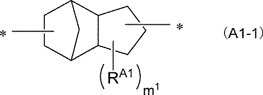
(式中、RA1は炭素数1~12のアルキル基を表し、上記脂環式骨格中のどこに置換していてもよい。m1は0~6の整数である。*は結合部位を示す。)
結合部位*を有する単結合は、脂環式骨格上のいずれの炭素原子に結合していてもよいが、下記一般式(A1-1’)中の1又は2のいずれかで示される炭素原子と、3又は4のいずれかで示される炭素原子に、それぞれ結合していることが好ましい。
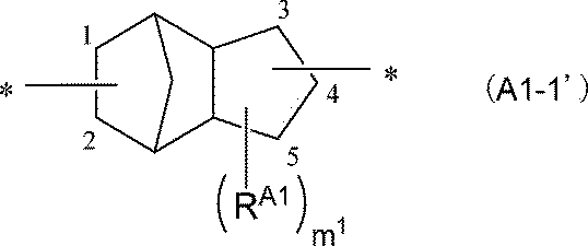
(式中、RA1、m1及び*は、上記一般式(A1-1)中のものと同じである。)
以下の説明で、(a1)エポキシ樹脂と(a2)(メタ)アクリロイル基含有有機酸とを反応させて得られる化合物を「(A’)成分」と称する場合がある。
また、(A’)成分に、(a3)飽和基又は不飽和基含有多塩基酸無水物を反応させることによって得られる化合物を「酸変性(メタ)アクリロイル基含有エポキシ樹脂誘導体」と称する場合がある。
以下、(A1)成分の好適な態様について説明する。
(a1)エポキシ樹脂は、2個以上のエポキシ基を有するものが好ましい。
(a1)エポキシ樹脂は、1種を単独で用いてもよく、2種以上を併用してもよい。
脂環式骨格を有するエポキシ樹脂が有する脂環式骨格については、前述した(A1)成分が有する脂環式骨格と同様に説明され、好ましい態様も同じである。
脂環式骨格を有するエポキシ樹脂としては、下記一般式(A1-2)で表されるエポキシ樹脂が好ましい。
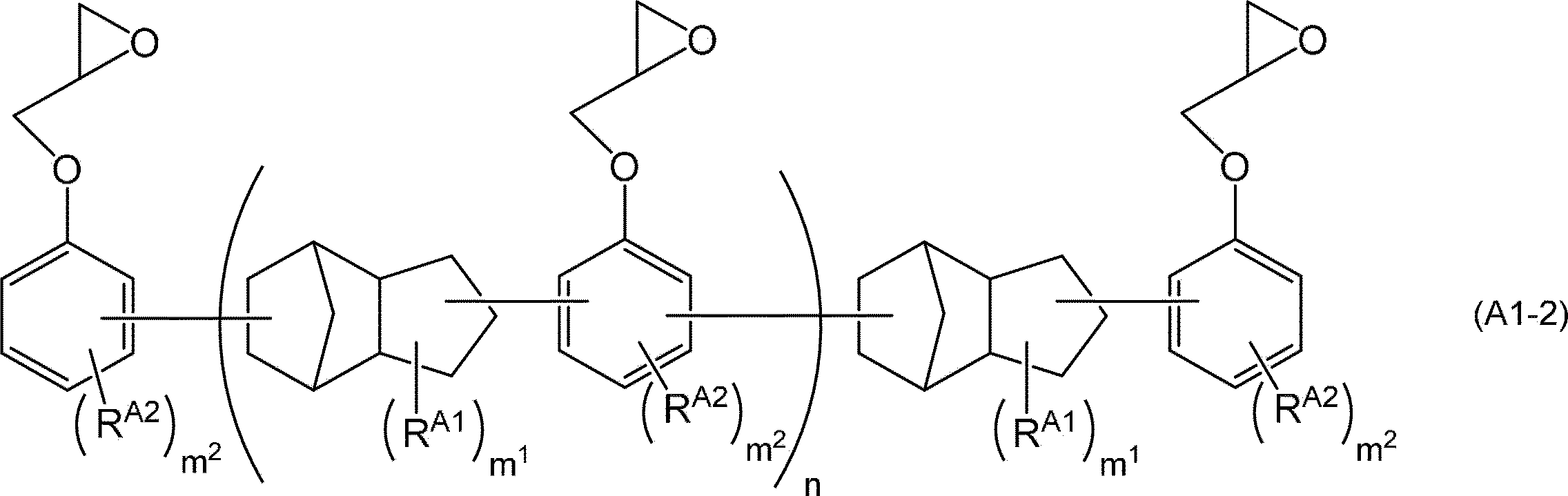
(式中、RA1は、各々独立に、炭素数1~12のアルキル基を表し、上記脂環式骨格中のどこに置換していてもよい。RA2は、各々独立に、炭素数1~12のアルキル基を表す。m1は0~6の整数、m2は0~3の整数である。nは0~50の数である。)
上記一般式(A1-2)中のRA2が表す炭素数1~12のアルキル基としては、例えば、メチル基、エチル基、n-プロピル基、イソプロピル基、n-ブチル基、イソブチル基、t-ブチル基、n-ペンチル基等が挙げられる。該アルキル基としては、炭素数1~6のアルキル基が好ましく、炭素数1~3のアルキル基がより好ましく、メチル基がさらに好ましい。
上記一般式(A1-2)中のm1は上記一般式(A1-1)中のm1と同じであり、好ましい態様も同じである。
上記一般式(A1-2)中のm2は0~3の整数であり、0又は1が好ましく、0がより好ましい。
上記一般式(A1-2)中のnは丸括弧内の構造単位の数を表し、0~50の数である。通常、エポキシ樹脂は丸括弧内の構造単位の数が異なるものの混合物となっているため、その場合、nはその混合物の平均値で表される。nとしては、0~30の数が好ましい。
ノボラック型エポキシ樹脂としては、例えば、ビスフェノールAノボラック型エポキシ樹脂、ビスフェノールFノボラック型エポキシ樹脂、ビスフェノールSノボラック型エポキシ樹脂等のビスフェノールノボラック型エポキシ樹脂;フェノールノボラック型エポキシ樹脂、クレゾールノボラック型エポキシ樹脂、ビフェニルノボラック型エポキシ樹脂、ナフトールノボラック型エポキシ樹脂などが挙げられる。
ノボラック型エポキシ樹脂としては、下記一般式(A1-3)で表される構造単位を有するエポキシ樹脂が好ましい。
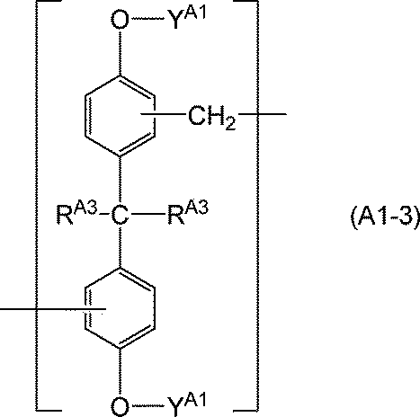
(式中、RA3は、各々独立に、水素原子又はメチル基を表し、YA1は、各々独立に、水素原子又はグリシジル基を表す。2つのYA1のうちの少なくとも一方はグリシジル基である。)
ビスフェノール型エポキシ樹脂としては、例えば、ビスフェノールA型エポキシ樹脂、ビスフェノールF型エポキシ樹脂、ビスフェノールS型エポキシ樹脂、3,3’,5,5’-テトラメチル-4,4’-ジグリシジルオキシジフェニルメタン等が挙げられる。
アラルキル型エポキシ樹脂としては、例えば、フェノールアラルキル型エポキシ樹脂、ビフェニルアラルキル型エポキシ樹脂、ナフトールアラルキル型エポキシ樹脂等が挙げられる。
その他のエポキシ樹脂としては、例えば、スチルベン型エポキシ樹脂、ナフタレン型エポキシ樹脂、ナフチレンエーテル型エポキシ樹脂、ビフェニル型エポキシ樹脂、ジヒドロアントラセン型エポキシ樹脂、シクロヘキサンジメタノール型エポキシ樹脂、トリメチロール型エポキシ樹脂、脂環式エポキシ樹脂、脂肪族鎖状エポキシ樹脂、複素環式エポキシ樹脂、スピロ環含有エポキシ樹脂、ゴム変性エポキシ樹脂等が挙げられる。
(a2)(メタ)アクリロイル基含有有機酸としては、(メタ)アクリロイル基含有モノカルボン酸が好ましい。
(メタ)アクリロイル基含有モノカルボン酸としては、例えば、アクリル酸、アクリル酸の二量体、メタクリル酸、β-フルフリルアクリル酸、β-スチリルアクリル酸、桂皮酸、クロトン酸、α-シアノ桂皮酸等のアクリル酸誘導体;水酸基含有アクリレートと二塩基酸無水物との反応生成物である半エステル化合物;(メタ)アクリロイル基含有モノグリシジルエーテル又は(メタ)アクリロイル基含有モノグリシジルエステルと二塩基酸無水物との反応生成物である半エステル化合物などが挙げられる。
(a2)成分は、1種を単独で用いてもよく、2種以上を併用してもよい。
(a3)成分としては、飽和基を含有するものであってもよいし、不飽和基を含有するものであってもよい。(a3)成分としては、例えば、無水コハク酸、無水マレイン酸、テトラヒドロ無水フタル酸、無水フタル酸、メチルテトラヒドロ無水フタル酸、エチルテトラヒドロ無水フタル酸、ヘキサヒドロ無水フタル酸、メチルヘキサヒドロ無水フタル酸、エチルヘキサヒドロ無水フタル酸、無水イタコン酸等が挙げられる。これらの中でも、解像性の観点から、テトラヒドロ無水フタル酸が好ましい。(a3)成分は、1種を単独で用いてもよく、2種以上を併用してもよい。
(A2)成分は、主に(A1)成分の架橋剤として用いられるものである。
本実施形態の感光性樹脂フィルムは、(A1)成分と共に(A2)成分を含有することによって、光ラジカル重合反応による架橋密度が高まり、アルカリ現像液耐性及び解像性が向上すると共に、耐熱性により優れる層間絶縁層を形成できる傾向にある。
なお、(A2)成分は、酸性置換基を有していてもよく、有していなくてもよい。
ここで、前記「XXX由来の骨格を有する(メタ)アクリレート化合物」(但し、XXXは化合物名である。)とは、XXXと(メタ)アクリル酸とのエステル化物を意味し、当該エステル化物には、アルキレンオキシ基で変性された化合物も包含される。
本実施形態の感光性樹脂フィルム中における(A)成分の含有量は、特に限定されないが、解像性及び形成される層間絶縁層の誘電特性の観点から、感光性樹脂フィルム中の樹脂成分全量基準で、好ましくは10~80質量%、より好ましくは15~60質量%、さらに好ましくは20~50質量%である。
ここで、本明細書において、「樹脂成分」とは、樹脂及び硬化反応によって樹脂を形成する化合物を意味する。例えば、本実施形態の感光性樹脂フィルムにおいては、(A)成分、(B)成分、(E)成分及び(F)成分は樹脂成分に分類される。
一方、(C)成分、(D)成分、(G)成分及び(H)成分は樹脂成分には含めないものとする。
樹脂組成物(1)中における(A)成分の含有量は、特に限定されないが、感光性樹脂フィルムの解像性及び形成される層間絶縁層の誘電特性の観点から、樹脂組成物(1)中の樹脂成分全量基準で、好ましくは10~80質量%、より好ましくは20~60質量%、さらに好ましくは30~50質量%である。
樹脂組成物(2)中における(A)成分の含有量は、特に限定されないが、解像性及び形成される層間絶縁層の誘電特性の観点から、樹脂組成物(2)中の樹脂成分全量基準で、好ましくは10~80質量%、より好ましくは15~60質量%、さらに好ましくは20~50質量%である。
(B)熱硬化性樹脂は、熱硬化性を有する樹脂であれば特に限定されない。
本実施形態の感光性樹脂フィルムが、(B)熱硬化性樹脂を含有することによって、形成される層間絶縁層の耐熱性が向上する傾向がある。
(B)熱硬化性樹脂は、1種を単独で用いてもよく、2種以上を併用してもよい。
エポキシ樹脂としては、2個以上のエポキシ基を有するエポキシ樹脂が好ましい。
エポキシ樹脂は、例えば、グリシジルエーテルタイプのエポキシ樹脂、グリシジルアミンタイプのエポキシ樹脂、グリシジルエステルタイプのエポキシ樹脂等に分類される。これらの中でも、グリシジルエーテルタイプのエポキシ樹脂が好ましい。
イソシアネート樹脂としては、例えば、トリメチレンジイソシアネート、テトラメチレンジイソシアネート、ペンタメチレンジイソシアネート、ヘキサメチレンジイソシアネート、トリメチルヘキサメチレンジイソシアネート等の脂肪族イソシアネート;1,3-シクロペンタンジイソシアネート、1,4-シクロヘキサンジイソシアネート、1,2-シクロヘキサンジイソシアネート、イソホロンジイソシアネート、ノルボルナンジイソシアネート等の脂環式イソシアネート;キシリレンジイソシアネート、2,4-トリレンジイソシアネート、2,6-トリレンジイソシアネート等の芳香族イソシアネート;これらのビューレット体;これらのヌレート体などが挙げられる。これらの中でも、脂肪族イソシアネートが好ましく、ヘキサメチレンジイソシアネートがより好ましい。
マレイミド樹脂としては、例えば、芳香環に直接結合するN-置換マレイミド基を有する芳香族マレイミド化合物、脂肪族炭化水素基に直接結合するN-置換マレイミド基を有する脂肪族マレイミド化合物等が挙げられる。これらの中でも、耐熱性及び取り扱い性の観点から、芳香族マレイミド化合物が好ましく、芳香族ビスマレイミド化合物がより好ましい。
芳香族マレイミド化合物としては、例えば、ビス(4-マレイミドフェニル)メタン、2,2-ビス[4-(4-マレイミドフェノキシ)フェニル]プロパン、3,3’-ジメチル-5,5’-ジエチル-4,4’-ジフェニルメタンビスマレイミド、ポリフェニルメタンマレイミド、ビフェニルアラルキル型マレイミド樹脂、インダン骨格を有する芳香族ビスマレイミド樹脂等が挙げられる。これらの中でも、インダン骨格を有する芳香族ビスマレイミド樹脂が好ましい。
本実施形態の感光性樹脂フィルム中における(B)熱硬化性樹脂の含有量は、特に限定されないが、導体接着性及び耐熱性により優れる層間絶縁層を形成するという観点から、感光性樹脂フィルム中の樹脂成分全量基準で、好ましくは1~60質量%、より好ましくは10~50質量%、さらに好ましくは15~40質量%である。
樹脂組成物(1)中における(B)熱硬化性樹脂の含有量は、特に限定されないが、導体接着性及び耐熱性により優れる層間絶縁層を形成するという観点から、樹脂組成物(1)中の樹脂成分全量基準で、好ましくは10~90質量%、より好ましくは30~80質量%、さらに好ましくは40~70質量%である。
樹脂組成物(1)中の質量基準でのエポキシ樹脂の含有量は、導体接着性により優れる層間絶縁層を形成するという観点から、樹脂組成物(2)中の質量基準でのエポキシ樹脂の含有量よりも多いことが好ましい。
樹脂組成物(2)中における(B)熱硬化性樹脂の含有量は、特に限定されないが、耐熱性及び誘電特性により優れる層間絶縁層を形成するという観点から、樹脂組成物(2)中の樹脂成分全量基準で、好ましくは1~50質量%、より好ましくは5~40質量%、さらに好ましくは10~30質量%である。
(C)光重合開始剤は、主に(A)成分が有するエチレン性不飽和基の光ラジカル重合反応の重合開始剤である。
本実施形態の感光性樹脂フィルムは(C)光重合開始剤を含有することによって、解像性がより一層向上する傾向がある。
(C)光重合開始剤は、1種を単独で用いてもよく、2種以上を併用してもよい。
本実施形態の感光性樹脂フィルム中における(C)光重合開始剤の含有量は、特に限定されないが、適度な重合反応の促進効果が得られ易いという観点から、感光性樹脂フィルム中の(A)成分100質量部に対して、好ましくは0.01~10質量部、より好ましくは0.05~5質量部、さらに好ましくは0.1~1質量部である。
樹脂組成物(1)中における(C)光重合開始剤の含有量は、特に限定されないが、適度な重合反応の促進効果が得られ易いという観点から、樹脂組成物(1)中の(A)成分100質量部に対して、好ましくは0.01~10質量部、より好ましくは0.05~5質量部、さらに好ましくは0.1~1質量部である。
樹脂組成物(2)中における(C)光重合開始剤の含有量は、特に限定されないが、適度な重合反応の促進効果が得られ易いという観点から、樹脂組成物(2)中の(A)成分100質量部に対して、好ましくは0.01~10質量部、より好ましくは0.05~5質量部、さらに好ましくは0.1~1質量部である。
本実施形態の感光性樹脂フィルムが(D)無機充填材を含有することによって、形成される層間絶縁層は、低熱膨張性、耐熱性及び難燃性がより一層向上する傾向にある。
(D)無機充填材は、1種を単独で用いてもよく、2種以上を併用してもよい。
シリカは、シランカップリング剤等のカップリング剤で表面処理されたものであってもよい。
(D1)成分であるシリカの真密度は、低熱膨張性の観点から、好ましくは1,500超、2,200kg/m3以下、より好ましくは1,600~2,200kg/m3、さらに好ましくは1,800~2,200kg/m3である。
(D2)成分であるシリカの真密度は、誘電特性の観点から、好ましくは1,000~1,500kg/m3、より好ましくは1,100~1,500kg/m3、さらに好ましくは1,200~1,500kg/m3、特に好ましくは1,250~1,450kg/m3、最も好ましくは1,250~1,400kg/m3である。
なお、シリカの真密度は、乾式自動密度計「AccuPycII 1340」(株式会社島津製作所製)によって測定することができる。
なお、本明細書において、体積平均粒子径(D50)は、サブミクロン粒子アナライザ(ベックマン・コールター株式会社製、商品名:N5)を用いて、国際標準規格ISO13321に準拠して、屈折率1.38で、溶剤中に分散した粒子を測定し、粒度分布における積算値50%(体積基準)に相当する粒子径として求めることができる。
本実施形態の感光性樹脂フィルム中における(D)無機充填材の含有量は、特に限定されないが、低熱膨張性、耐熱性、難燃性及び導体接着性により優れる層間絶縁層を形成するという観点から、好ましくは2~60質量%、より好ましくは3質量%以上60質量%未満、さらに好ましくは4~55質量%、よりさらに好ましくは5~50質量%、特に好ましくは6~40質量%である。
樹脂組成物(1)中における(D)無機充填材の含有量は、特に限定されないが、低熱膨張性、耐熱性、難燃性及び導体接着性により優れる層間絶縁層を形成するという観点から、樹脂組成物(1)の固形分全量に対して、好ましくは5~70質量%、より好ましくは15~60質量%、さらに好ましくは25~50質量%である。
樹脂組成物(1)中のシリカの質量基準での含有量は、導体接着性により優れる層間絶縁層を形成するという観点から、樹脂組成物(2)中の質量基準でのシリカの含有量よりも多いことが好ましい。
樹脂組成物(2)中における(D)無機充填材の含有量は、特に限定されないが、低熱膨張性、耐熱性及び難燃性により優れる層間絶縁層を形成するという観点から、樹脂組成物(2)の固形分全量に対して、好ましくは1~60質量%、より好ましくは2質量%以上60質量%未満、さらに好ましくは3~55質量%、よりさらに好ましくは4~50質量%、特に好ましくは5~40質量%である。
本実施形態の感光性樹脂フィルムが(E)フッ素含有樹脂を含有することによって、本実施形態の感光性樹脂フィルムから形成される層間絶縁層は、比誘電率が低減する傾向がある。
(E)フッ素含有樹脂は、1種を単独で用いてもよく、2種以上を併用してもよい。
含フッ素オレフィンは、炭素-水素結合のうちの一部の水素原子がフッ素原子によって置換されたオレフィンであってもよいが、比誘電率をより低減する観点から、全ての炭素-水素結合の水素原子がフッ素原子によって置換されたオレフィンが好ましい。
粒子である(E)フッ素含有樹脂の体積平均粒子径(D50)は、特に限定されないが、解像性の観点から、好ましくは0.01~3.0μm、より好ましくは0.05~2.5μm、さらに好ましくは0.1~2.0μmである。
本実施形態の感光性樹脂フィルム中における(E)フッ素含有樹脂の含有量は、特に限定されないが、耐熱性及び導体接着性により優れる層間絶縁層を形成するという観点から、感光性樹脂フィルム中の樹脂成分全量基準で、好ましくは5~80質量%、より好ましくは10~70質量%、さらに好ましくは15~60質量%である。
樹脂組成物(1)は、(E)フッ素含有樹脂を含有していてもよいが、解像性の観点、及び導体接着性により優れる層間絶縁層を形成するという観点からは、(E)フッ素含有樹脂を含有しないことが好ましい。
樹脂組成物(1)が(E)フッ素含有樹脂を含有する場合、樹脂組成物(1)中の(E)フッ素含有樹脂の含有量は、少ない程好ましく、上記と同様の観点から、樹脂組成物(1)中の樹脂成分全量基準で、好ましくは20質量%以下、より好ましくは10質量%以下、さらに好ましくは1質量%以下である。
樹脂組成物(2)中の(E)フッ素含有樹脂の含有量は、特に限定されないが、解像性の観点、並びに絶縁信頼性、比誘電率、耐熱性及び導体接着性により優れる層間絶縁層を形成するという観点から、樹脂組成物(2)中の樹脂成分全量基準で、好ましくは10~80質量%、より好ましくは15~70質量%、さらに好ましくは20~65質量%である。
本実施形態の感光性樹脂フィルムは、さらに、(F)エラストマーを含有していてもよい。
本実施形態の感光性樹脂フィルムが、(F)エラストマーを含有することによって、形成される層間絶縁層は、導体接着性がより一層向上する傾向がある。
なお、ここでの「エラストマー」とは、JIS K 6240:2011に従って示差走査熱量測定で測定したガラス転移温度が25℃以下である高分子を意味する。
(F)エラストマーは、1種を単独で用いてもよく、2種以上を併用してもよい。
ポリブタジエン系エラストマーは、解像性の観点から、酸無水物基を有するポリブタジエン系エラストマーであることが好ましく、無水マレイン酸に由来する酸無水物基を有するポリブタジエン系エラストマーであることがより好ましい。
ポリブタジエン系エラストマーが酸無水物基を有する場合、1分子中に有する酸無水物基の数は、特に限定されないが、解像性の観点、及び比誘電率により優れる層間絶縁層を形成するという観点から、好ましくは1~12個、より好ましくは3~11個、さらに好ましくは6~10個である。
なお、本明細書において、数平均分子量(Mn)は、テトラヒドロフランを溶媒としたゲルパーミエーションクロマトグラフィー(GPC)法によって、標準ポリスチレン換算することで求めた値であり、詳細には、実施例に記載の方法に従って測定した値である。
本実施形態の感光性樹脂フィルム中における(F)エラストマーの含有量は、特に限定されないが、耐熱性及び導体接着性により優れる層間絶縁層を形成するという観点から、感光性樹脂フィルム中の樹脂成分全量基準で、好ましくは0.5~20質量%、より好ましくは1~15質量%、さらに好ましくは2~10質量%である。
樹脂組成物(1)が(F)エラストマーを含有する場合、樹脂組成物(1)中の(F)エラストマーの含有量は、特に限定されないが、耐熱性及び導体接着性により優れる層間絶縁層を形成するという観点から、樹脂組成物(1)中の樹脂成分全量基準で、好ましくは1~30質量%、より好ましくは3~20質量%、さらに好ましくは5~15質量%である。
樹脂組成物(2)が(F)エラストマーを含有する場合、樹脂組成物(2)中の(F)エラストマーの含有量は、特に限定されないが、耐熱性及び導体接着性により優れる層間絶縁層を形成するという観点から、樹脂組成物(2)中の樹脂成分全量基準で、好ましくは0.5~20質量%、より好ましくは1~15質量%、さらに好ましくは2~10質量%である。
本実施形態の感光性樹脂フィルムは、さらに、(G)有機過酸化物を含有することが好ましい。(G)有機過酸化物は、主に(A)成分、及び必要に応じて(B)成分が有するエチレン性不飽和基の熱ラジカル重合反応の重合開始剤である。
本実施形態の感光性樹脂フィルムが、(G)有機過酸化物を含有することによって、形成される層間絶縁層は、耐熱性、誘電特性等をより一層向上できる傾向がある。
(G)有機過酸化物は、1種を単独で用いてもよく、2種以上を併用してもよい。
本実施形態の感光性樹脂フィルムが(G)有機過酸化物を含有する場合、その含有量は、特に限定されないが、耐熱性及び導体接着性により優れる層間絶縁層を形成するという観点から、感光性樹脂フィルム中の(A)成分100質量部に対して、好ましくは0.1~10質量部、より好ましくは1~7質量部、さらに好ましくは1.5~4質量部である。
樹脂組成物(1)が(G)有機過酸化物を含有する場合、樹脂組成物(1)中の(G)有機過酸化物の含有量は、特に限定されないが、耐熱性及び導体接着性により優れる層間絶縁層を形成するという観点から、樹脂組成物(1)中の(A)成分100質量部に対して、好ましくは0.1~10質量部、より好ましくは1~7質量部、さらに好ましくは1.5~4質量部である。
樹脂組成物(2)が(G)有機過酸化物を含有する場合、樹脂組成物(2)中の(G)有機過酸化物の含有量は、特に限定されないが、耐熱性及び導体接着性により優れる層間絶縁層を形成するという観点から、樹脂組成物(2)中の(A)成分100質量部に対して、好ましくは0.1~10質量部、より好ましくは1~7質量部、さらに好ましくは1.5~4質量部である。
本実施形態の感光性樹脂フィルムは、さらに、(H)硬化促進剤を含有することが好ましい。
本実施形態の感光性樹脂フィルムが、(H)硬化促進剤を含有することによって、形成される層間絶縁層は、耐熱性、誘電特性等をより一層向上できる傾向がある。
(H)硬化促進剤は、1種を単独で用いてもよく、2種以上を併用してもよい。
これらの中でも、優れた硬化作用を得るという観点から、イミダゾール系化合物が好ましい。
本実施形態の感光性樹脂フィルムが(H)硬化促進剤を含有する場合、その含有量は、特に限定されないが、耐熱性及び導体接着性により優れる層間絶縁層を形成するという観点から、感光性樹脂フィルム中の(B)成分100質量部に対して、好ましくは0.1~10質量部、より好ましくは0.5~7質量部、さらに好ましくは1~4質量部である。
樹脂組成物(1)が(H)硬化促進剤を含有する場合、樹脂組成物(1)中の(H)硬化促進剤の含有量は、特に限定されないが、耐熱性及び導体接着性により優れる層間絶縁層を形成するという観点から、樹脂組成物(1)中の(B)成分100質量部に対して、好ましくは0.1~10質量部、より好ましくは0.5~7質量部、さらに好ましくは1~4質量部である。
樹脂組成物(2)が(H)硬化促進剤を含有する場合、樹脂組成物(2)中の(H)硬化促進剤の含有量は、特に限定されないが、耐熱性及び導体接着性により優れる層間絶縁層を形成するという観点から、樹脂組成物(2)中の(B)成分100質量部に対して、好ましくは0.1~10質量部、より好ましくは0.5~7質量部、さらに好ましくは1~4質量部である。
本実施形態の感光性樹脂フィルムは、必要に応じて、(I)その他の成分として、上記各成分以外の成分を含有していてもよい。
(I)その他の成分としては、例えば、上記各成分以外の樹脂;(E)成分以外の有機充填材;光増感剤;重合禁止剤;整泡剤;顔料;メラミン等の接着助剤;シリコーン化合物等の整泡剤;増粘剤;難燃剤などが挙げられる。
これらは、各々について、1種を単独で用いてもよく、2種以上を併用してもよい。
本実施形態の感光性樹脂フィルム中における(I)その他の成分の含有量は、各々の目的に応じて適宜調整すればよいが、各々について、0.01~10質量%であってもよく、0.05~5質量%であってもよく、0.1~1質量%であってもよい。
本実施形態の感光性樹脂フィルムは、例えば、樹脂組成物(1)及び樹脂組成物(2)を用いて製造することができる。
樹脂組成物(1)及び樹脂組成物(2)は、各層に配合する成分、及び必要に応じて使用する希釈剤を混合することによって製造できる。各成分の混合には、例えば、ロールミル、ビーズミル、プラネタリミキサー、自公転ミキサー等を使用することができる。
別の方法としては、キャリアフィルム上にいずれか一方の樹脂組成物を塗布しておき、当該一方の樹脂組成物上に、いずれか他方の樹脂組成物を塗布することによっても、本実施形態の感光性樹脂フィルムを製造することができる。一方の樹脂組成物を塗布した後、他方の樹脂組成物を塗布する前に、必要に応じて乾燥を行ってもよい。
樹脂組成物(1)及び樹脂組成物(2)の塗膜を乾燥する場合における乾燥温度は、特に限定されないが、好ましくは60~150℃、より好ましくは70~120℃、さらに好ましくは80~100℃である。また、乾燥時間としては、特に限定されないが、好ましくは1~60分間、より好ましくは2~30分間、さらに好ましくは5~20分間である。
本実施形態のプリント配線板は、本実施形態の感光性樹脂フィルムの硬化物である層間絶縁層を有する、プリント配線板である。
なお、本実施形態のプリント配線板が有する「層間絶縁層」とは、例えば、ビア及び配線の形成、粗化処理等の各種加工又は処理が施された後の状態のものも含まれる。
(1):本実施形態の感光性樹脂フィルムを、前記第二表面が貼付面になる状態で、回路基板の片面又は両面にラミネートすること(以下、「ラミネート工程(1)」ともいう)。
(2):前記(1)でラミネートされた感光性樹脂フィルムを露光及び現像することによって、ビアを有する層間絶縁層を形成すること(以下、「ビア形成工程(2)」ともいう)。
(3):前記ビアを有する層間絶縁層を加熱硬化させること(以下、「加熱硬化工程(3)」ともいう)。
(4):前記層間絶縁層の前記回路基板と反対側の面上に回路パターンを形成すること(以下、「回路パターン形成工程(4)」ともいう)。
以下、適宜、図1を参照しながら、本実施形態のプリント配線板の製造方法について説明する。
なお、本明細書において、便宜上、所定の操作について「XX工程」と称することがあるが、該「XX工程」は、本明細書に具体的に記載された態様のみに限定されるものではない。
ラミネート工程(1)では、本実施形態の感光性樹脂フィルムを、前記第二表面が貼付面になる状態で、回路基板の片面又は両面にラミネートする。
図1(a)には、回路パターン102を有する基板101の両面に感光層103を形成する工程が図示されている。
感光層103は、本実施形態の感光性樹脂フィルムを、第二表面が貼付面になるように基板101の両面にラミネートすることによって形成することができる。
ラミネートは、例えば、真空ラミネーター等を用いて加圧及び加熱しながら圧着すればよい。
ラミネート後、感光層103にキャリアフィルムが貼付されている場合、キャリアフィルムは後述する露光前に剥離してもよいし、露光後に剥離してもよい。
ビア形成工程(2)では、ラミネート工程(1)で形成された感光層を露光及び現像することによって、ビアを有する層間絶縁層を形成する。
図1(b)には、感光層103を露光及び現像することによって、ビア105を有する層間絶縁層104を形成する工程が図示されている。
感光層103を露光することによって、光ラジカル重合反応を開始させて、感光性樹脂フィルムを硬化させる。
活性光線の光源としては、例えば、カーボンアーク灯、水銀蒸気アーク灯、高圧水銀灯、キセノンランプ、アルゴンレーザー等のガスレーザー;YAGレーザー等の固体レーザー;半導体レーザー等の紫外線又は可視光線を有効に放射するものなどの公知の光源が挙げられる。
露光量は、使用する光源及び感光層の厚さ等によって適宜調整すればよい。例えば、高圧水銀灯からの紫外線照射を用いて、厚さ1~100μmの感光層を露光する場合、露光量は、特に限定されないが、好ましくは10~1,000mJ/cm2、より好ましくは50~700mJ/cm2、さらに好ましくは150~400mJ/cm2である。
現像方法は、ウェット現像であっても、ドライ現像であってもよいが、ウェット現像が好ましい。ウェット現像による方法としては、解像性向上の観点から、スプレー方式が好ましい。
現像液としては、例えば、アルカリ性水溶液、水系現像液、有機溶剤系現像液等が挙げられ、これらの中でもアルカリ性水溶液が好ましい。
露光及び現像後、層間絶縁層の硬化度を高める観点から、後露光を行ってもよい。後露光における露光量は、特に限定されないが、好ましくは0.2~10J/cm2、より好ましくは0.5~5J/cm2である。
本実施形態のフォトリソグラフィー法によるビアの形成では、断面形状が逆台形のビアを形成することができる。当該形状を有するビアは、めっき銅のビア壁面への付き回り性が高いため好ましい。
本実施形態のフォトリソグラフィー法によるビアの形成では、ビアの直径をレーザー加工によって作製するビアの直径よりも小さくすることができる。本実施形態の製造方法によって形成されるビアの直径は、例えば、40μm以下であってもよく、35μm以下であってもよく、30μm以下であってもよい。ビアの直径の下限値に特に制限はないが、例えば、15μm以上であってもよいし、20μm以上であってもよい。
加熱硬化工程(3)では、ビアを有する層間絶縁層を加熱硬化させる。
すなわち、加熱硬化工程(3)では、加熱によって、本実施形態の感光性樹脂フィルムに含有される熱硬化性を有する成分の硬化反応を進行させる。
加熱温度は、特に限定されないが、好ましくは100~300℃、より好ましくは120~200℃、さらに好ましくは150~180℃である。加熱時間は、特に限定されないが、好ましくは0.3~3時間、より好ましくは0.5~2時間、さらに好ましくは0.75~1.5時間である。
次に、上記で形成した層間絶縁層の回路基板と反対側の面上に回路パターンを形成する。層間絶縁層の回路基板と反対側の面は、硬化後の第一表面に相当する表面である。
回路パターンは、微細配線形成の観点から、粗化処理、シード層の形成、レジストパターンの形成、銅の回路層の形成及びレジストパターンの除去をこの順で行う、セミアディティブプロセスにより形成することが好ましい。
シード層106は電解銅めっきを施すための給電層を形成するためのものである。
シード層106は、ビア底、ビア壁面及び層間絶縁層の表面全体にパラジウム触媒等を用いて無電解銅めっき処理を施すことによって形成することができる。
レジストパターン107は、例えば、シード層106上にドライフィルムレジストをロールラミネーター等を用いて熱圧着し、これを露光及び現像することによって形成することができる。ドライフィルムレジストとしては市販品を使用することができる。
銅の回路層108は、電解銅めっきによって形成することが好ましい。
電解銅めっきに用いる電解銅めっき液としては、例えば、硫酸銅を含む電解銅めっき液等、市販の電解銅めっき液を用いることができる。
電解銅めっき後、アルカリ水溶液又はアミン系剥離剤を用いてレジストパターン107を除去し、さらに、配線間のシード層106を除去するフラッシュエッチング、パラジウム触媒の除去等を公知の方法によって適宜行う。さらに、必要に応じて、未反応の熱硬化成分を十分に熱硬化させるためのポストベーク処理を行ってもよい。
ソルダーレジスト層109は、公知のソルダーレジスト用の感光性樹脂フィルムを用いて形成することができる。
本実施形態の半導体パッケージは、本実施形態のプリント配線板を有する半導体パッケージである。
本実施形態の半導体パッケージは、例えば、本実施形態のプリント配線板の所定の位置に半導体チップ、メモリ等の半導体素子を搭載し、封止樹脂等によって半導体素子を封止することによって製造することができる。
酸価は、測定対象を中和するのに要した水酸化カリウム水溶液の量から算出した。
重量平均分子量(Mw)及び数平均分子量(Mn)は、下記のGPC測定装置及び測定条件で測定し、標準ポリスチレンの検量線を使用して換算して求めた。検量線の作成は、標準ポリスチレンとして5サンプルセット(「PStQuick MP-H」及び「PStQuick B」、東ソー株式会社製)を用いた。
(GPC測定装置)
GPC装置:高速GPC装置「HCL-8320GPC」、検出器は示差屈折計又はUV、東ソー株式会社製
カラム :カラムTSKgel SuperMultipore HZ-H(カラム長さ:15cm、カラム内径:4.6mm)、東ソー株式会社製
(測定条件)
溶媒 :テトラヒドロフラン(THF)
測定温度 :40℃
流量 :0.35ml/分
試料濃度 :10mg/THF5ml
注入量 :20μl
各例で製造したキャリアフィルム付き感光性樹脂フィルムに対して、両面のキャリアフィルムを有したまま、平面露光機を用いて、光量400mJ/cm2(波長365nm)の紫外線を照射した。その後、両面のキャリアフィルムを剥離除去し、UVコンベア式露光機を用いて、光量2J/cm2(波長365nm)の紫外線を照射した。次いで、温風循環式乾燥機を用いて、170℃で1時間加熱して、感光性樹脂フィルムの硬化物を得た。得られた感光性樹脂フィルムの硬化物を、包埋樹脂で埋め込み硬化した後、研磨機(リファインテック株式会社製、商品名「リファインポリッシャー」)を用いて研磨して、感光性樹脂フィルムの硬化物の断面を削り出したものを試験片とした。
次に、元素分析装置としてエネルギー分散型蛍光X線分析装置(EDX:Energy dispersive X-ray spectroscopy)を備える走査型電子顕微鏡(SEM)(株式会社日立ハイテク社製、商品名「SU-5000」)を用いて、上記感光性樹脂フィルムの硬化物の断面を3,000倍で観察した。なお、図2に、感光性樹脂フィルムの硬化物の断面像10の一例を示す。
図2に示す断面像10において、一方の表面に相当する基準ラインBL1、他方の表面に相当する基準ラインBL2を特定した。
なお、基準ラインBL1又は基準ラインBL2を特定する表面に凹凸が存在する場合は、断面像の全範囲において、等間隔になるように各層の表面位置を少なくとも10点プロットし、これを最小二乗法によって近似することで得られる直線を、基準ラインBL1又は基準ラインBL2とすることができる。
基準ラインBL1から硬化物の内側に向けて1μm離間した、基準ラインBL1と平行の測定ラインL1、及び、基準ラインBL2から硬化物の内側に向けて1μm離間した、基準ラインBL2と平行の測定ラインL2上の各々において、上記の元素分析装置を用いて元素分析を行った。なお、元素分析を行うライン長さは、各々40μmとした。算出された平均フッ素原子濃度のうち、いずれか低い方のフッ素原子濃度を、第一表面のフッ素原子濃度として特定し、いずれか高い方のフッ素原子濃度を、第二表面のフッ素原子濃度として特定した。
実施例1~6、比較例1~3
表1に示す配合組成(表中の数値の単位は質量部であり、溶液の場合は固形分換算量である。)に従って各成分を配合し、3本ロールミル及び自公転ミキサーを使用して混練した。その後、固形分濃度が65質量%になるようにメチルエチルケトンを加えて、樹脂組成物(1)、樹脂組成物(2)を、各々得た。
次に、樹脂組成物(1)を、キャリアフィルム(PETフィルム、帝人株式会社製、商品名「G2-16」、厚さ16μm)上に塗布し、熱風対流式乾燥機を用いて、100℃で10分間乾燥して、キャリアフィルム付きの樹脂組成物(1)フィルム(樹脂組成物(1)フィルムの厚さ5μm)を形成した。
また、樹脂組成物(2)を、上記とは別のキャリアフィルム(帝人株式会社製のPETフィルム、商品名「G2-16」、厚さ16μm)上に塗布し、熱風対流式乾燥機を用いて、100℃で10分間乾燥して、キャリアフィルム付きの樹脂組成物(2)フィルム(樹脂組成物(2)フィルムの厚さ20μm)を形成した。
上記で得られたキャリアフィルム付きの樹脂組成物(1)フィルム及びキャリアフィルム付きの樹脂組成物(2)フィルムの樹脂組成物フィルム同士を貼り合わせることによって、キャリアフィルム付き感光性樹脂フィルム(感光性樹脂フィルムの厚さ25μm)を得た。
各例で製造したキャリアフィルム付き感光性樹脂フィルムの第二表面側のキャリアフィルムを剥離除去したものを2枚準備し、第二表面同士を貼り合わせた。
次いで、両面のキャリアフィルムを有したまま、平面露光機を用いて、光量400mJ/cm2(波長365nm)の紫外線を照射した。次いで、両面のキャリアフィルムを剥離除去し、UVコンベア式露光機を用いて、光量2J/cm2(波長365nm)の紫外線を照射した。その後、温風循環式乾燥機を用いて、170℃で1時間加熱し、7cm×10cmのサイズに切断したものを、比誘電率(Dk)及び誘電正接(Df)の測定サンプルとした。
上記で得られた測定サンプルを、温風循環式乾燥機を用いて、105℃で10分間乾燥してから、スプリットポスト誘電体共振器法(SPDR法)を用いて、10GHz帯で比誘電率(Dk)及び誘電正接(Df)を測定し、以下の基準で評価した。
(比誘電率(Dk)の評価基準)
A:2.8以下
B:2.8超~3.0以下
C:3.0超
(誘電正接(Df)の評価基準)
A:0.0100以下
B:0.0100超~0.0120以下
C:0.0120超
(1)評価用積層体の作製
銅箔(厚さ12μm)をガラスエポキシ基材に積層したプリント配線板用基板(昭和電工マテリアルズ株式会社製、商品名「MCL-E-679」)の銅箔表面を、粗化前処理液(メック株式会社製、商品名「CZ-8100」)によって粗化前処理した後、水洗及び乾燥した。次に、各例で製造したキャリアフィルム付き感光性樹脂フィルムの第二表面側のキャリアフィルムを剥離除去し、露出した第二表面が貼付面になるようにして、上記粗化前処理済のプリント配線板用基板の銅箔上にラミネートした。なお、ラミネートには、プレス式真空ラミネーター(株式会社名機製作所製、商品名「MVLP-500」)を用い、ラミネートの条件は、プレス熱板温度70℃、真空引き時間20秒、ラミネートプレス時間30秒、気圧4kPa以下、圧着圧力0.4MPaとした。ラミネート処理後、室温で1時間以上放置することによって、プリント配線板用基板の銅箔表面上に、感光性樹脂フィルム及びキャリアフィルムがこの順に積層された評価用積層体を得た。
(2)感度測定
上記で得た評価用積層体のキャリアフィルム上に、41段ステップタブレットを配置した。次いで、超高圧水銀ランプを光源としたダイレクトイメージング露光装置(株式会社オーク製作所製、商品名「DXP-3512」)を用いて露光を行った。露光パターンは、φ30~100μmまでのドットが格子状に配列したドットパターンを用いた。
露光後、室温で30分間放置した後、上記で得た評価用積層体の第一表面側のキャリアフィルムを除去し、30℃の1質量%炭酸ナトリウム水溶液を用いて、未露光部の感光性樹脂フィルムを60秒間スプレー現像した。現像後、41段ステップタブレットの光沢残存ステップ段数が4.0になる露光エネルギー量を、感光性樹脂フィルムの感度(単位:mJ/cm2)とした。この感度で露光したパターンを用いて、下記評価基準に従って評価した。
(3)ビアの解像性の評価
ビアの解像性は、上記(2)で求めた感光性樹脂フィルムの感度である露光エネルギー量で露光及びスプレー現像して形成されたビアパターンを、光学顕微鏡を用いて観察し、下記基準に従って評価した。
(評価基準)
A:ドットパターンのφ60μmビア部分が開口している。
C:ドットパターンのφ60μmビア部分が開口していない。
(1)評価用積層体の作製及び感光性樹脂フィルムの感度測定
上記[ビアの解像性の評価]の(1)及び(2)の手順において、使用した露光機を、超高圧水銀ランプを光源とした平行光露光機(株式会社オーク製作所製、商品名「EXM-1201」)に変更したこと以外は、上記[ビアの解像性の評価]の(1)及び(2)の手順と同様に操作を行い、評価用積層体を準備すると共に、光沢残存ステップ段数が8.0となる露光エネルギー量を求め、これを感光性樹脂フィルムの感度(単位;mJ/cm2)とした。
(2)露光工程及び現像工程
評価用積層体の第一表面側のキャリアフィルムを剥離除去し、上記で求めた感度である露光エネルギー量で全面露光を行い、感光性樹脂フィルムを硬化させた。露光後、室温で30分間放置した後、30℃の1質量%炭酸ナトリウム水溶液を用いて、未露光部の感光性樹脂フィルムを60秒間スプレー現像した。
(3)ポストキュア処理
続いて、高圧水銀灯ランプ照射タイプのUVコンベア装置(株式会社オーク製作所製)を用いて、露光量が2J/cm2となるコンベア速度でポストUVキュアを行った。その後、温風循環式乾燥機を用いて、170℃で1時間加熱した。
(4)粗化処理
上記加熱後の評価用積層体を、膨潤液「スウェリングディップセキュリガントP」を用いて70℃で5分間処理してから、粗化液「ドージングセキュリガントP500J」を用いて70℃で10分間、粗化処理した。続いて、中和液「リダクションコンディショナーセキュリガントP500」を用いて50℃で5分間、中和処理を行った。その後、バッファードフッ酸「LAL1800 SA 高純度バッファードフッ酸」を用いて、室温で10分間フッ酸処理を行った。なお、膨潤液、粗化液及び中和液は、いずれもアトテックジャパン株式会社製のもの、バッファードフッ酸はステラケミファ株式会社製のものを用いた。
(5)めっき処理
上記粗化処理後の評価用積層体に対して、無電解めっき液「プリガントMSK-DK」(アトテックジャパン株式会社製)を用いて、無電解めっき処理を30℃で15分間を行った。次いで、電気めっき液「カパラシドHL」(アトテックジャパン株式会社製)を用いて、電気めっき処理を24℃、2A/dm2で1.5時間行って、層間絶縁層上にめっき銅を形成した。なお、めっき銅の厚さは25μmとした。
(6)めっき銅との接着強度の測定
めっき銅との接着強度は、JIS C6481:1996に準拠して、23℃にて垂直引き剥がし強さを測定し、下記基準に従って評価した。
(評価基準)
A:0.4kN/m超
B:0.1kN/m超~0.4kN/m以下
C:0.1kN/m以下

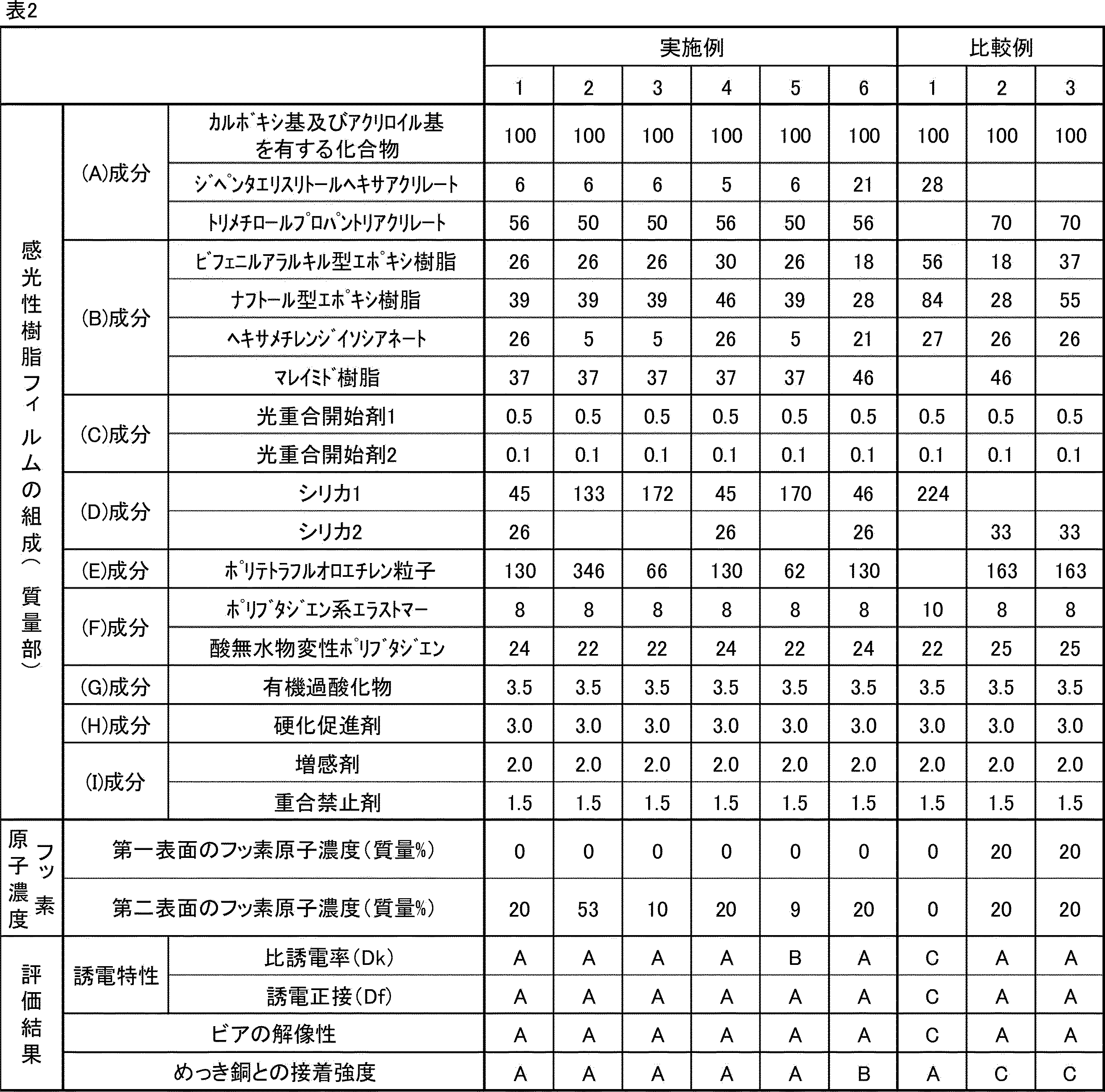
・カルボキシ基及びアクリロイル基を有する化合物:日本化薬株式会社製、商品名「ZXR-1807H」、酸価:110mgKOH/g、重量平均分子量(Mw):2,000
・ビフェニルアラルキル型エポキシ樹脂:日本化薬株式会社製、商品名「NC-3000-L」、エポキシ基当量:272g/eq
・ナフトール型エポキシ樹脂:新日鐵住金株式会社製、商品名「ESN-475V」、エポキシ基当量:325g/eq
・マレイミド樹脂:インダン骨格を有する芳香族ビスマレイミド樹脂
・光重合開始剤1:フェニルビス(2,4,6-トリメチルベンゾイル)ホスフィンオキシド
・光重合開始剤2:1-[9-エチル-6-(2-メチルベンゾイル)-9H-カルバゾール-3-イル]エタノン1-(O-アセチルオキシム)
・シリカ1:株式会社アドマテックス製、商品名「SC2050-MB」、平均粒子径(D50):0.5μm、真密度2,200kg/m3
・シリカ2:TAT社製、商品名「BQQ-0710SCB」、平均粒子径(D50):0.7μm、真密度1,350kg/m3
・ポリテトラフルオロエチレン粒子:三菱鉛筆株式会社製、商品名「MPT-N8」、平均粒子径(D50):0.2~0.3μm
・ポリブタジエン系エラストマー:ブタジエン・スチレン・ランダムコポリマー、Cray Valley社製、商品名「Ricon100」、数平均分子量(Mn):4,500
・酸無水物変性ポリブタジエン:Cray Valley社製、商品名「Ricon131MA17」、数平均分子量(Mn):5,400、1分子中に有する酸無水物基の数:9
・有機過酸化物:1,3-ジ(t-ブチルパーオキシイソプロピル)ベンゼン
・硬化促進剤:1-ベンジル-2-フェニルイミダゾール
・増感剤:4,4’-ビス-(ジエチルアミノ)ベンゾフェノン
・重合禁止剤:4-tert-ブチルピロカテコール
BL2 基準ライン
L1 測定ライン
L2 測定ライン
10 断面像
100A 多層プリント配線板
101 基板
102 回路パターン
103 感光層
104 層間絶縁層
105 ビア
106 シード層
107 レジストパターン
108 銅の回路層
109 ソルダーレジスト層
Claims (12)
- (A)エチレン性不飽和基を有する化合物、(B)熱硬化性樹脂、(C)光重合開始剤、(D)無機充填材及び(E)フッ素含有樹脂を含有する感光性樹脂フィルムであって、
前記感光性樹脂フィルムは、第一表面と、該第一表面の反対側の第二表面と、を有し、
前記第一表面から深さ1μmの部位におけるフッ素原子濃度が、前記第二表面から深さ1μmの部位におけるフッ素原子濃度よりも低い、感光性樹脂フィルム。 - 前記(A)エチレン性不飽和基を有する化合物として、エチレン性不飽和基及び酸性置換基を有する化合物を含有する、請求項1に記載の感光性樹脂フィルム。
- 前記(B)熱硬化性樹脂として、エポキシ樹脂、マレイミド樹脂、アリル樹脂及びビニル樹脂からなる群から選択される1種以上を含有する、請求項1に記載の感光性樹脂フィルム。
- 前記(D)無機充填材としてシリカを含有し、該シリカの含有量が、2~60質量%である、請求項1に記載の感光性樹脂フィルム。
- 前記(D)無機充填材として、真密度が1,500kg/m3以下であるシリカを含有する、請求項1に記載の感光性樹脂フィルム。
- 前記(E)フッ素含有樹脂の含有量が、前記感光性樹脂フィルムの樹脂成分全量基準で、5~80質量%である、請求項1に記載の感光性樹脂フィルム。
- さらに、(F)エラストマーを含有する、請求項1に記載の感光性樹脂フィルム。
- 前記第一表面が、銅めっきによって回路パターンが形成される面であり、前記第二表面が、前記感光性樹脂フィルムを積層する際の貼付面である、請求項1に記載の感光性樹脂フィルム。
- フォトビアを有する層間絶縁層の形成に用いられる、請求項1に記載の感光性樹脂フィルム。
- 請求項1に記載の感光性樹脂フィルムの硬化物である層間絶縁層を有する、プリント配線板。
- 請求項10に記載のプリント配線板を有する、半導体パッケージ。
- 下記(1)~(4)を含む、プリント配線板の製造方法。
(1):請求項1~9のいずれか1項に記載の感光性樹脂フィルムを、前記第二表面が貼付面になる状態で、回路基板の片面又は両面にラミネートすること。
(2):前記(1)でラミネートされた感光性樹脂フィルムを露光及び現像することによって、ビアを有する層間絶縁層を形成すること。
(3):前記ビアを有する層間絶縁層を加熱硬化させること。
(4):前記層間絶縁層の前記回路基板と反対側の面に回路パターンを形成すること。
Priority Applications (3)
| Application Number | Priority Date | Filing Date | Title |
|---|---|---|---|
| JP2024512756A JPWO2023190800A1 (ja) | 2022-03-31 | 2023-03-30 | |
| US18/849,889 US20250226236A1 (en) | 2022-03-31 | 2023-03-30 | Photosensitive resin film, printed wiring board, semiconductor package, and method for producing printed wiring board |
| CN202380030798.1A CN118946852A (zh) | 2022-03-31 | 2023-03-30 | 感光性树脂膜、印刷布线板、半导体封装及印刷布线板的制造方法 |
Applications Claiming Priority (2)
| Application Number | Priority Date | Filing Date | Title |
|---|---|---|---|
| JP2022060844 | 2022-03-31 | ||
| JP2022-060844 | 2022-03-31 |
Publications (1)
| Publication Number | Publication Date |
|---|---|
| WO2023190800A1 true WO2023190800A1 (ja) | 2023-10-05 |
Family
ID=88202625
Family Applications (1)
| Application Number | Title | Priority Date | Filing Date |
|---|---|---|---|
| PCT/JP2023/013043 Ceased WO2023190800A1 (ja) | 2022-03-31 | 2023-03-30 | 感光性樹脂フィルム、プリント配線板、半導体パッケージ及びプリント配線板の製造方法 |
Country Status (5)
| Country | Link |
|---|---|
| US (1) | US20250226236A1 (ja) |
| JP (1) | JPWO2023190800A1 (ja) |
| CN (1) | CN118946852A (ja) |
| TW (1) | TW202348640A (ja) |
| WO (1) | WO2023190800A1 (ja) |
Citations (7)
| Publication number | Priority date | Publication date | Assignee | Title |
|---|---|---|---|---|
| JP2005055655A (ja) * | 2003-08-04 | 2005-03-03 | Fuji Photo Film Co Ltd | 感光性転写シート |
| JP2006285179A (ja) * | 2005-03-09 | 2006-10-19 | Fuji Photo Film Co Ltd | 感光性永久レジストフィルム及び永久パターン形成方法 |
| JP2013173841A (ja) * | 2012-02-24 | 2013-09-05 | Ajinomoto Co Inc | 樹脂組成物 |
| JP2017088438A (ja) * | 2015-11-06 | 2017-05-25 | 花王株式会社 | 中空シリカ粒子の製造方法 |
| JP2019179200A (ja) * | 2018-03-30 | 2019-10-17 | 太陽インキ製造株式会社 | 硬化性樹脂組成物、ドライフィルム、硬化物およびプリント配線板 |
| WO2021253727A1 (zh) * | 2020-06-18 | 2021-12-23 | 苏州锦艺新材料科技有限公司 | 低介电空心二氧化硅微球的制备方法 |
| JP2022025366A (ja) * | 2020-07-29 | 2022-02-10 | 太陽インキ製造株式会社 | ドライフィルム、ドライフィルムセット、その硬化物および電子部品 |
Family Cites Families (1)
| Publication number | Priority date | Publication date | Assignee | Title |
|---|---|---|---|---|
| JP4720000B2 (ja) * | 2001-04-10 | 2011-07-06 | 日立化成工業株式会社 | 感光性樹脂組成物、この組成物を用いた感光性フィルム |
-
2023
- 2023-03-30 WO PCT/JP2023/013043 patent/WO2023190800A1/ja not_active Ceased
- 2023-03-30 US US18/849,889 patent/US20250226236A1/en active Pending
- 2023-03-30 JP JP2024512756A patent/JPWO2023190800A1/ja active Pending
- 2023-03-30 CN CN202380030798.1A patent/CN118946852A/zh active Pending
- 2023-03-31 TW TW112112416A patent/TW202348640A/zh unknown
Patent Citations (7)
| Publication number | Priority date | Publication date | Assignee | Title |
|---|---|---|---|---|
| JP2005055655A (ja) * | 2003-08-04 | 2005-03-03 | Fuji Photo Film Co Ltd | 感光性転写シート |
| JP2006285179A (ja) * | 2005-03-09 | 2006-10-19 | Fuji Photo Film Co Ltd | 感光性永久レジストフィルム及び永久パターン形成方法 |
| JP2013173841A (ja) * | 2012-02-24 | 2013-09-05 | Ajinomoto Co Inc | 樹脂組成物 |
| JP2017088438A (ja) * | 2015-11-06 | 2017-05-25 | 花王株式会社 | 中空シリカ粒子の製造方法 |
| JP2019179200A (ja) * | 2018-03-30 | 2019-10-17 | 太陽インキ製造株式会社 | 硬化性樹脂組成物、ドライフィルム、硬化物およびプリント配線板 |
| WO2021253727A1 (zh) * | 2020-06-18 | 2021-12-23 | 苏州锦艺新材料科技有限公司 | 低介电空心二氧化硅微球的制备方法 |
| JP2022025366A (ja) * | 2020-07-29 | 2022-02-10 | 太陽インキ製造株式会社 | ドライフィルム、ドライフィルムセット、その硬化物および電子部品 |
Also Published As
| Publication number | Publication date |
|---|---|
| JPWO2023190800A1 (ja) | 2023-10-05 |
| CN118946852A (zh) | 2024-11-12 |
| US20250226236A1 (en) | 2025-07-10 |
| TW202348640A (zh) | 2023-12-16 |
Similar Documents
| Publication | Publication Date | Title |
|---|---|---|
| KR102959152B1 (ko) | 감광성 수지 조성물, 감광성 수지 필름, 다층 프린트 배선판 및 반도체 패키지, 및 다층 프린트 배선판의 제조 방법 | |
| WO2018003313A1 (ja) | 樹脂組成物、樹脂シート、多層プリント配線板及び半導体装置 | |
| WO2018003314A1 (ja) | 樹脂組成物、樹脂シート、多層プリント配線板及び半導体装置 | |
| JP7831289B2 (ja) | 感光性樹脂組成物、感光性樹脂フィルム、多層プリント配線板及び半導体パッケージ、並びに多層プリント配線板の製造方法 | |
| TW202442699A (zh) | 感光性樹脂組成物、感光性樹脂薄膜、印刷線路板及半導體封裝體 | |
| JP7768359B2 (ja) | 感光性樹脂フィルム、プリント配線板、半導体パッケージ及びプリント配線板の製造方法 | |
| JP7768358B2 (ja) | 感光性多層樹脂フィルム、プリント配線板、半導体パッケージ及びプリント配線板の製造方法 | |
| JP6972495B2 (ja) | 樹脂組成物、樹脂シート、多層プリント配線板及び半導体装置 | |
| WO2024185060A1 (ja) | 感光性樹脂組成物、感光性樹脂フィルム、多層プリント配線板及び半導体パッケージ、並びに多層プリント配線板の製造方法 | |
| WO2023190810A1 (ja) | 感光性樹脂フィルム、プリント配線板、半導体パッケージ及びプリント配線板の製造方法 | |
| WO2023190798A1 (ja) | 感光性多層樹脂フィルム、プリント配線板、半導体パッケージ及びプリント配線板の製造方法 | |
| WO2023190811A1 (ja) | 感光性多層樹脂フィルム、プリント配線板、半導体パッケージ及びプリント配線板の製造方法 | |
| US20250226236A1 (en) | Photosensitive resin film, printed wiring board, semiconductor package, and method for producing printed wiring board | |
| WO2025084264A1 (ja) | 感光性多層樹脂フィルム、プリント配線板、半導体パッケージ及びプリント配線板の製造方法 | |
| WO2025084265A1 (ja) | 感光性樹脂フィルム、プリント配線板、半導体パッケージ及びプリント配線板の製造方法 | |
| JP2025018036A (ja) | 感光性樹脂組成物、感光性樹脂フィルム、プリント配線板、半導体パッケージ及び光重合性化合物 | |
| JP7859442B2 (ja) | 感光性樹脂組成物、感光性樹脂フィルム、多層プリント配線板及び半導体パッケージ、並びに多層プリント配線板の製造方法 | |
| WO2024219251A1 (ja) | プリント配線板の製造方法、感光性樹脂組成物、感光性樹脂フィルム、プリント配線板及び半導体パッケージ | |
| KR20260061436A (ko) | 감광성 다층 수지 필름, 프린트 배선판, 반도체 패키지 및 프린트 배선판의 제조 방법 | |
| TW202436484A (zh) | 感光性樹脂組成物、感光性樹脂薄膜、多層印刷線路板及半導體封裝體、以及多層印刷線路板的製造方法 | |
| WO2023031986A1 (ja) | 感光性樹脂組成物、感光性樹脂フィルム、多層プリント配線板及び半導体パッケージ、並びに多層プリント配線板の製造方法 | |
| WO2023031987A1 (ja) | 感光性樹脂組成物、感光性樹脂フィルム、多層プリント配線板及び半導体パッケージ、並びに多層プリント配線板の製造方法 |
Legal Events
| Date | Code | Title | Description |
|---|---|---|---|
| 121 | Ep: the epo has been informed by wipo that ep was designated in this application |
Ref document number: 23780808 Country of ref document: EP Kind code of ref document: A1 |
|
| ENP | Entry into the national phase |
Ref document number: 2024512756 Country of ref document: JP Kind code of ref document: A |
|
| WWE | Wipo information: entry into national phase |
Ref document number: 18849889 Country of ref document: US |
|
| WWE | Wipo information: entry into national phase |
Ref document number: 202380030798.1 Country of ref document: CN |
|
| NENP | Non-entry into the national phase |
Ref country code: DE |
|
| 122 | Ep: pct application non-entry in european phase |
Ref document number: 23780808 Country of ref document: EP Kind code of ref document: A1 |
|
| WWP | Wipo information: published in national office |
Ref document number: 18849889 Country of ref document: US |