WO2023190786A1 - 流路構造体および半導体製造装置 - Google Patents
流路構造体および半導体製造装置 Download PDFInfo
- Publication number
- WO2023190786A1 WO2023190786A1 PCT/JP2023/013014 JP2023013014W WO2023190786A1 WO 2023190786 A1 WO2023190786 A1 WO 2023190786A1 JP 2023013014 W JP2023013014 W JP 2023013014W WO 2023190786 A1 WO2023190786 A1 WO 2023190786A1
- Authority
- WO
- WIPO (PCT)
- Prior art keywords
- metal wiring
- thermocouple
- metal
- flow path
- section
- Prior art date
- Legal status (The legal status is an assumption and is not a legal conclusion. Google has not performed a legal analysis and makes no representation as to the accuracy of the status listed.)
- Ceased
Links
Images






Classifications
-
- H—ELECTRICITY
- H01—ELECTRIC ELEMENTS
- H01J—ELECTRIC DISCHARGE TUBES OR DISCHARGE LAMPS
- H01J37/00—Discharge tubes with provision for introducing objects or material to be exposed to the discharge, e.g. for the purpose of examination or processing thereof
- H01J37/32—Gas-filled discharge tubes
- H01J37/32431—Constructional details of the reactor
- H01J37/32715—Workpiece holder
- H01J37/32724—Temperature
-
- H—ELECTRICITY
- H10—SEMICONDUCTOR DEVICES; ELECTRIC SOLID-STATE DEVICES NOT OTHERWISE PROVIDED FOR
- H10P—GENERIC PROCESSES OR APPARATUS FOR THE MANUFACTURE OR TREATMENT OF DEVICES COVERED BY CLASS H10
- H10P72/00—Handling or holding of wafers, substrates or devices during manufacture or treatment thereof
- H10P72/06—Apparatus for monitoring, sorting, marking, testing or measuring
- H10P72/0602—Temperature monitoring
-
- C—CHEMISTRY; METALLURGY
- C23—COATING METALLIC MATERIAL; COATING MATERIAL WITH METALLIC MATERIAL; CHEMICAL SURFACE TREATMENT; DIFFUSION TREATMENT OF METALLIC MATERIAL; COATING BY VACUUM EVAPORATION, BY SPUTTERING, BY ION IMPLANTATION OR BY CHEMICAL VAPOUR DEPOSITION, IN GENERAL; INHIBITING CORROSION OF METALLIC MATERIAL OR INCRUSTATION IN GENERAL
- C23C—COATING METALLIC MATERIAL; COATING MATERIAL WITH METALLIC MATERIAL; SURFACE TREATMENT OF METALLIC MATERIAL BY DIFFUSION INTO THE SURFACE, BY CHEMICAL CONVERSION OR SUBSTITUTION; COATING BY VACUUM EVAPORATION, BY SPUTTERING, BY ION IMPLANTATION OR BY CHEMICAL VAPOUR DEPOSITION, IN GENERAL
- C23C16/00—Chemical coating by decomposition of gaseous compounds, without leaving reaction products of surface material in the coating, i.e. chemical vapour deposition [CVD] processes
- C23C16/44—Chemical coating by decomposition of gaseous compounds, without leaving reaction products of surface material in the coating, i.e. chemical vapour deposition [CVD] processes characterised by the method of coating
-
- C—CHEMISTRY; METALLURGY
- C23—COATING METALLIC MATERIAL; COATING MATERIAL WITH METALLIC MATERIAL; CHEMICAL SURFACE TREATMENT; DIFFUSION TREATMENT OF METALLIC MATERIAL; COATING BY VACUUM EVAPORATION, BY SPUTTERING, BY ION IMPLANTATION OR BY CHEMICAL VAPOUR DEPOSITION, IN GENERAL; INHIBITING CORROSION OF METALLIC MATERIAL OR INCRUSTATION IN GENERAL
- C23C—COATING METALLIC MATERIAL; COATING MATERIAL WITH METALLIC MATERIAL; SURFACE TREATMENT OF METALLIC MATERIAL BY DIFFUSION INTO THE SURFACE, BY CHEMICAL CONVERSION OR SUBSTITUTION; COATING BY VACUUM EVAPORATION, BY SPUTTERING, BY ION IMPLANTATION OR BY CHEMICAL VAPOUR DEPOSITION, IN GENERAL
- C23C16/00—Chemical coating by decomposition of gaseous compounds, without leaving reaction products of surface material in the coating, i.e. chemical vapour deposition [CVD] processes
- C23C16/44—Chemical coating by decomposition of gaseous compounds, without leaving reaction products of surface material in the coating, i.e. chemical vapour deposition [CVD] processes characterised by the method of coating
- C23C16/50—Chemical coating by decomposition of gaseous compounds, without leaving reaction products of surface material in the coating, i.e. chemical vapour deposition [CVD] processes characterised by the method of coating using electric discharges
- C23C16/505—Chemical coating by decomposition of gaseous compounds, without leaving reaction products of surface material in the coating, i.e. chemical vapour deposition [CVD] processes characterised by the method of coating using electric discharges using radio frequency discharges
-
- G—PHYSICS
- G01—MEASURING; TESTING
- G01K—MEASURING TEMPERATURE; MEASURING QUANTITY OF HEAT; THERMALLY-SENSITIVE ELEMENTS NOT OTHERWISE PROVIDED FOR
- G01K7/00—Measuring temperature based on the use of electric or magnetic elements directly sensitive to heat ; Power supply therefor, e.g. using thermoelectric elements
- G01K7/02—Measuring temperature based on the use of electric or magnetic elements directly sensitive to heat ; Power supply therefor, e.g. using thermoelectric elements using thermoelectric elements, e.g. thermocouples
-
- H—ELECTRICITY
- H01—ELECTRIC ELEMENTS
- H01J—ELECTRIC DISCHARGE TUBES OR DISCHARGE LAMPS
- H01J37/00—Discharge tubes with provision for introducing objects or material to be exposed to the discharge, e.g. for the purpose of examination or processing thereof
- H01J37/32—Gas-filled discharge tubes
- H01J37/32431—Constructional details of the reactor
- H01J37/32458—Vessel
- H01J37/32522—Temperature
-
- H—ELECTRICITY
- H01—ELECTRIC ELEMENTS
- H01J—ELECTRIC DISCHARGE TUBES OR DISCHARGE LAMPS
- H01J37/00—Discharge tubes with provision for introducing objects or material to be exposed to the discharge, e.g. for the purpose of examination or processing thereof
- H01J37/32—Gas-filled discharge tubes
- H01J37/32431—Constructional details of the reactor
- H01J37/32532—Electrodes
-
- H—ELECTRICITY
- H10—SEMICONDUCTOR DEVICES; ELECTRIC SOLID-STATE DEVICES NOT OTHERWISE PROVIDED FOR
- H10P—GENERIC PROCESSES OR APPARATUS FOR THE MANUFACTURE OR TREATMENT OF DEVICES COVERED BY CLASS H10
- H10P14/00—Formation of materials, e.g. in the shape of layers or pillars
- H10P14/60—Formation of materials, e.g. in the shape of layers or pillars of insulating materials
-
- H—ELECTRICITY
- H10—SEMICONDUCTOR DEVICES; ELECTRIC SOLID-STATE DEVICES NOT OTHERWISE PROVIDED FOR
- H10P—GENERIC PROCESSES OR APPARATUS FOR THE MANUFACTURE OR TREATMENT OF DEVICES COVERED BY CLASS H10
- H10P50/00—Etching of wafers, substrates or parts of devices
- H10P50/20—Dry etching; Plasma etching; Reactive-ion etching
- H10P50/24—Dry etching; Plasma etching; Reactive-ion etching of semiconductor materials
- H10P50/242—Dry etching; Plasma etching; Reactive-ion etching of semiconductor materials of Group IV materials
-
- H—ELECTRICITY
- H10—SEMICONDUCTOR DEVICES; ELECTRIC SOLID-STATE DEVICES NOT OTHERWISE PROVIDED FOR
- H10P—GENERIC PROCESSES OR APPARATUS FOR THE MANUFACTURE OR TREATMENT OF DEVICES COVERED BY CLASS H10
- H10P72/00—Handling or holding of wafers, substrates or devices during manufacture or treatment thereof
- H10P72/04—Apparatus for manufacture or treatment
- H10P72/0402—Apparatus for fluid treatment
- H10P72/0418—Apparatus for fluid treatment for etching
- H10P72/0421—Apparatus for fluid treatment for etching for drying etching
-
- H—ELECTRICITY
- H10—SEMICONDUCTOR DEVICES; ELECTRIC SOLID-STATE DEVICES NOT OTHERWISE PROVIDED FOR
- H10P—GENERIC PROCESSES OR APPARATUS FOR THE MANUFACTURE OR TREATMENT OF DEVICES COVERED BY CLASS H10
- H10P72/00—Handling or holding of wafers, substrates or devices during manufacture or treatment thereof
- H10P72/70—Handling or holding of wafers, substrates or devices during manufacture or treatment thereof for supporting or gripping
-
- H—ELECTRICITY
- H10—SEMICONDUCTOR DEVICES; ELECTRIC SOLID-STATE DEVICES NOT OTHERWISE PROVIDED FOR
- H10P—GENERIC PROCESSES OR APPARATUS FOR THE MANUFACTURE OR TREATMENT OF DEVICES COVERED BY CLASS H10
- H10P95/00—Generic processes or apparatus for manufacture or treatments not covered by the other groups of this subclass
Definitions
- the disclosed embodiments relate to a flow path structure and a semiconductor manufacturing apparatus.
- Patent Document 1 describes that a semiconductor wafer is placed on a mounting table on which a temperature sensor S1 is mounted as an example of a sensor, and temperature data in the vicinity of the semiconductor wafer is obtained. It is also described that the temperature sensor S2 is disposed on the back surface of the shower plate.
- the flow path structure of the present disclosure includes a base, a flow path, a plurality of openings, a first metal wiring, and a second metal wiring.
- the base has a first surface and is made of ceramic.
- the flow path is located inside the base body and has a plurality of branch paths. A plurality of openings are located on the first surface and are connected to the plurality of branch paths, respectively.
- the first metal wiring is at least partially located inside the base and is made of a first metal.
- the second metal wiring is at least partially located inside the base and is made of a second metal different from the first metal.
- the first metal wiring and the second metal wiring constitute a thermocouple section that is connected inside the base body and has a thermocouple function. When the first surface is viewed from the front, the first metal wiring and the second metal wiring surround the opening, and the thermocouple section is located around the opening.
- FIG. 1 is a cross-sectional view showing an example of the configuration of a semiconductor manufacturing apparatus according to an embodiment.
- FIG. 2 is a perspective view showing an example of the configuration of the flow path structure according to the embodiment.
- FIG. 3 is a front view showing an example of the configuration of the channel structure according to the embodiment.
- FIG. 4 is a cross-sectional view taken along line AA shown in FIG.
- FIG. 5 is a front view showing an example of the configuration of the thermocouple section according to the embodiment.
- FIG. 6 is a cross-sectional view showing an example of the configuration of the thermocouple section according to the embodiment.
- FIG. 7 is a cross-sectional view showing an example of the configuration of the thermocouple section according to the embodiment.
- FIG. 1 is a cross-sectional view showing an example of the configuration of a semiconductor manufacturing apparatus according to an embodiment.
- FIG. 2 is a perspective view showing an example of the configuration of the flow path structure according to the embodiment.
- FIG. 3 is a front view
- FIG. 8 is a cross-sectional view showing an example of the configuration of the thermocouple section according to the embodiment.
- FIG. 9 is a front view showing another example of the configuration of the thermocouple section according to the embodiment.
- FIG. 10 is a sectional view showing another example of the configuration of the thermocouple section according to the embodiment.
- FIG. 11 is a sectional view showing another example of the configuration of the thermocouple section according to the embodiment.
- FIG. 12 is a front view showing an example of the configuration of a flow path structure according to Modification 1 of the embodiment.
- FIG. 13 is a cross-sectional view showing an example of the configuration of a flow path structure according to Modification 2 of the embodiment.
- FIG. 14 is a front view showing an example of the configuration of a flow path structure according to Modification 3 of the embodiment.
- FIG. 15 is a front view showing an example of the configuration of a flow path structure according to Modification 3 of the embodiment.
- FIG. 16 is a front view showing an example of the configuration of a flow path structure according to Modification 4 of the embodiment.
- FIG. 17 is an enlarged sectional view showing an example of the configuration of a flow path structure according to modification 5 of the embodiment.
- FIG. 18 is an enlarged sectional view showing an example of the configuration of a flow path structure according to modification 6 of the embodiment.
- a technology has been disclosed in which a temperature sensor is used to acquire temperature data within the semiconductor manufacturing equipment to perform a process while estimating various process data.
- FIG. 1 is a cross-sectional view showing an example of the configuration of a semiconductor manufacturing apparatus 100 according to an embodiment.
- the semiconductor manufacturing apparatus 100 is, for example, a plasma processing apparatus that processes a semiconductor wafer W using plasma.
- a semiconductor manufacturing apparatus 100 include a CVD (Chemical Vapor Deposition) apparatus and a dry etching apparatus.
- the semiconductor manufacturing apparatus 100 includes a flow path structure 1, a chamber 110, a mounting table 120, and a shaft 130.
- the chamber 110 accommodates the channel structure 1, at least a portion of the mounting table 120, and at least a portion of the shaft 130.
- the inside of the chamber 110 can be evacuated or depressurized using an exhaust section (not shown) or the like. Further, an opening 111 for loading and unloading the semiconductor wafer W is located on the side of the chamber 110.
- the mounting table 120 is located below the channel structure 1 in the chamber 110.
- the mounting table 120 supports the semiconductor wafer W on the surface facing the channel structure 1, here, the upper surface of the mounting table 120.
- the shaft 130 supports the flow path structure 1 inside the chamber 110 and introduces a medium such as a process gas into the inside of the flow path structure 1.
- a through hole 131 is formed inside the shaft 130, and the through hole 131 is connected to the opening 3 of the channel structure 1 (see FIG. 2).
- the mounting table 120 and the shaft 130 may be made of ceramics. For example, aluminum oxide or aluminum nitride may be used as the ceramic.
- a process gas used for plasma processing is supplied to the chamber 110 from the through hole 131 of the shaft 130, through the flow path 4 of the flow path structure 1 (see FIG. 4), and from the plurality of openings 5 (see FIG. 3). is derived inside. That is, the flow path structure 1 according to the embodiment functions as a shower plate in the semiconductor manufacturing apparatus 100, for example.
- FIG. 2 is a perspective view showing an example of the configuration of the channel structure 1 according to the embodiment
- FIG. 3 is a front view showing an example of the structure of the channel structure 1 according to the embodiment.
- FIG. 4 is a sectional view taken along the line AA shown in FIG. 3.
- the channel structure 1 includes a base 2, an opening 3 formed in the base 2, a channel 4, and a plurality of openings 5.
- the base 2 has a disk shape, for example, and has a first surface 2a and a second surface 2b.
- the lower surface is the first surface 2a
- the upper surface is the second surface 2b.
- the shape of the base 2 is not limited to the disk shape, and may be any shape.
- the opening 3 is located on the second surface 2b of the base 2, and the plurality of openings 5 are located on the first surface 2a of the base 2.
- the opening 3 and the plurality of openings 5 are connected by a flow path 4.
- the opening 3 is located at the center of the second surface 2b of the base 2, as shown in FIG.
- the plurality of openings 5 may be located so as to be evenly distributed over the entire first surface 2a of the base body 2, as shown in FIG.
- the present disclosure has shown an example in which one opening 3 is provided as an inflow port for a medium such as a process gas, and a plurality of openings 5 are provided as a medium discharge port, the present disclosure is limited to such an example. do not have. For example, a plurality of openings 3 may be provided, or one opening 5 may be provided.
- the flow path 4 includes, in order from the side connected to the opening 3, an introduction path 4a, a widened path 4b, and a plurality of branch paths 4c.
- the introduction path 4a is, for example, a portion extending from the opening 3 perpendicularly to the second surface 2b.
- the widening path 4b is, for example, a portion that extends from the end of the introduction path 4a on the first surface 2a side in parallel to the first surface 2a.
- the plurality of branch paths 4c are, for example, portions extending from the widened path 4b to the plurality of openings 5, respectively. Note that the configuration of the flow path 4 in the present disclosure is not limited to the example shown in FIG. 4.
- the base body 2 according to the embodiment may be made of any material such as resin, metal, and ceramics.
- the base body 2 is made of ceramics, it is superior to resins and metals in terms of mechanical strength, heat resistance, corrosion resistance, and the like.
- ceramics include aluminum oxide ceramics, zirconium oxide ceramics, yttrium oxide ceramics, magnesium oxide ceramics, silicon nitride ceramics, aluminum nitride ceramics, silicon carbide ceramics, cordierite ceramics, or mullite ceramics. etc.
- an aluminum oxide ceramic is one that contains 70% by mass or more of aluminum oxide out of 100% by mass of all components constituting the ceramic. Note that the same applies to other ceramics.
- the material of the target substrate can be confirmed by the following method.
- the target substrate is measured using an X-ray diffraction device (XRD), and the obtained 2 ⁇ value, which is the diffraction angle, is compared with the JCPDS card.
- XRD X-ray diffraction device
- the target substrate is made of aluminum oxide ceramics.
- the flow path structure 1 of the present disclosure includes a plurality of openings 5 and the base body 2 is made of ceramics, a shower plate used in a semiconductor manufacturing apparatus 100 (see FIG. 1) that requires corrosion resistance. It can be suitably used for. Furthermore, since the flow path structure 1 according to the embodiment has little deterioration in the quality of the inflowing gas, the quality of the processed material is high.
- thermocouple section 10 includes a first metal wiring 11 (see FIG. 5) made of a first metal, and a second metal wiring 12 (see FIG. 5) made of a second metal different from the first metal. It has a thermocouple function.
- thermocouple sections 10 by locating a plurality of thermocouple sections 10 inside the base 2, a plurality of temperature measurement points can be provided within the shower plate. Thereby, the temperature inside the shower plate can be measured, and the temperature distribution inside the shower plate can also be measured.
- thermocouple sections 10 are located at different distances from the center of the first surface 2a.
- one thermocouple section 10 is located at the center of the first surface 2a, and another thermocouple section 10 is located at the end of the first surface 2a.
- the plurality of thermocouple sections 10 may be located at different distances from the opening 111 (see FIG. 1) of the chamber 110 (see FIG. 1).
- the thermocouple section 10 may be located at a portion of the base 2 closer to the opening 111 and at a portion of the base 2 farther from the opening 111.
- the temperature distribution inside the chamber 110 can be measured with high accuracy.
- FIG. 4 shows an example in which the widened path 4b is disk-shaped, the present disclosure is not limited to such an example, and a support may be provided in the widened path 4b.
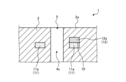
- FIG. 5 is a front view showing an example of the configuration of the thermocouple section 10 according to the embodiment
- FIG. 6 is a sectional view showing an example of the configuration of the thermocouple section 10 according to the embodiment. Further, FIG. 6 is a sectional view taken along the line BB shown in FIG.
- thermocouple section 10 is constructed at a portion where a first metal wiring 11 made of a first metal and a second metal wiring 12 made of a second metal are in contact with each other.
- the first metal and the second metal may include, for example, W (tungsten) and Re (rhenium), and may be configured such that the ratios of W and Re are different from each other. Thereby, it is possible to generate an electromotive force due to the Seebeck effect in the portions of the first metal wiring 11 and the second metal wiring 12 that are in contact with each other.
- thermocouple part 10 Although this alloy is not specified by industrial standards such as JIS as a material for forming the thermocouple part 10, it has a melting point of 3000°C or higher, so it can be fired at the same time as the ceramics forming the base 2. In addition, since the electromotive force is large, a commercially available thermocouple temperature measurement instrument can be used as is.
- the material of the first metal wiring 11 and the second metal wiring 12 is not limited to an alloy containing W and Re, but may also include Pt (platinum) and Rh (rhodium). It may be an alloy, an alloy containing Ni (nickel) and Cr (chromium), or an alloy standardized by JIS C1602.
- the materials of the first metal wiring 11 and the second metal wiring 12 have a large electromotive force and different resistance temperature coefficients from the viewpoint of improving measurement accuracy, and are suitable for the firing temperature of the ceramics constituting the base body 2. Any alloy that has a high melting point and can be used in commercially available instruments may be used.
- a tape made of ceramics and containing a binder is prepared. Note that, if necessary, the shape may be processed using a tool, a mold, or a laser.
- the tape is printed and filled with a conductive paste that will become the first metal wiring 11 and the second metal wiring 12.
- the flow path structure 1 can be obtained by stacking the tapes after drying, degreasing and baking them under conditions depending on the material of the tapes.
- thermocouple portion 10 can be easily formed inside the base 2 by using such a tape lamination method. Furthermore, in the embodiment, by forming the thermocouple section 10 inside the base body 2 using a printed conductive paste, calibration of the thermocouple section 10 can be made unnecessary even after long-term use.
- the first metal wiring 11 may include a surrounding portion 11a, a wiring portion 11b, and a via portion 11c (see FIG. 14).
- the enclosing portion 11a is located so as to surround the branch road 4c.
- the surrounding portion 11a may seamlessly surround the entire circumference of the branch road 4c.
- the wiring portion 11b is located so as to extend parallel to the first surface 2a of the base 2 (see FIG. 6).
- the via portion 11c is located so as to extend perpendicularly to the first surface 2a of the base 2.
- the second metal wiring 12 has a surrounding part 12a, a wiring part 12b, and a via part 12c (see FIG. 14).
- the enclosing portion 12a is located so as to surround the branch road 4c.
- the wiring portion 12b is located so as to extend parallel to the first surface 2a of the base 2.
- the wiring portion 12b is positioned so as to ride over the surrounding portion 11a of the first metal wiring 11.
- the via portion 12c is located so as to extend perpendicularly to the first surface 2a of the base 2.
- the enclosing part 11a and the enclosing part 12a are located so as to concentrically surround the outside of the branch path 4c. Furthermore, the enclosing part 11a and the enclosing part 12a are located so as to be in contact with each other. As a result, a circular thermocouple portion 10 is formed at a portion where the surrounding portion 11a and the surrounding portion 12a are in contact with each other.
- thermocouple section 10 is located around the opening 5.
- the temperature of the branch path 4c and the opening 5 through which the process gas is discharged can be measured with high accuracy.
- thermocouple section 10 may surround the opening 5 when the first surface 2a is viewed from the front. Thereby, the temperature in the vicinity of the branch passage 4c and the opening 5 through which the process gas is discharged can be measured with higher accuracy.
- thermocouple section 10 shown in FIG. 5 is not limited to the example shown in FIG. 6.
- 7 and 8 are cross-sectional views showing an example of the configuration of the thermocouple section 10 according to the embodiment, and correspond to FIG. 6 described above. As shown in FIG. 7, in the embodiment, a portion may be cut out so that the surrounding part 11a of the first metal wiring 11 is divided into wiring parts 12b of the second metal wiring 12.
- the first metal wiring 11 and the second metal wiring 12 may be positioned so as to be laminated inside the base 2. Then, the thermocouple section 10 may be formed by stacking the surrounding part 12a of the second metal wiring 12 in contact with the surrounding part 11a of the first metal wiring 11.
- the first metal wiring 11 and the second metal wiring 12 are located in an overlapping manner in the thermocouple part 10, thereby making contact between the surrounding part 11a and the surrounding part 12a.
- the area can be increased.
- the temperature in the vicinity of the branch path 4c and the opening 5 through which the process gas is discharged can be measured with higher accuracy.
- the planar shape of the thermocouple section 10 is not limited to the example shown in FIG. 5.
- FIG. 9 is a front view showing another example of the configuration of the thermocouple section 10 according to the embodiment
- FIG. 10 is a sectional view showing another example of the configuration of the thermocouple section 10 according to the embodiment.
- FIG. 10 is a sectional view taken along the line CC shown in FIG.
- the semicircular enclosing part 11a and the semicircular enclosing part 12a are connected to each other to form a circular shape, so that the first metal wiring 11 and the second metal
- the wiring 12 may be positioned so as to surround the opening 5 as a whole.
- thermocouple portion 10 even if the portion where the first metal wiring 11 and the second metal wiring 12 are in contact with each other, that is, the thermocouple portion 10 is located apart, the distance is 1 (cm) or less. If the two thermocouple sections are located at a distance of , and are connected to the same first metal wiring 11 and second metal wiring 12, it can be considered as one thermocouple section 10.
- thermocouple section 10 shown in FIG. 9 is not limited to the example shown in FIG. 10.
- FIG. 11 is a sectional view showing another example of the configuration of the thermocouple section 10 according to the embodiment.
- the first metal wiring 11 and the second metal wiring 12 may be positioned so as to be laminated inside the base 2. Then, the thermocouple section 10 may be formed by stacking the surrounding part 12a of the second metal wiring 12 in contact with the surrounding part 11a of the first metal wiring 11.
- the first metal wiring 11 and the second metal wiring 12 are located in an overlapping manner in the thermocouple part 10, thereby making contact between the surrounding part 11a and the surrounding part 12a.
- the area can be increased.
- the temperature in the vicinity of the branch path 4c and the opening 5 through which the process gas is discharged can be measured with higher accuracy.
- thermocouple section 10 may have a region containing the first metal and the second metal. That is, in the embodiment, the thermocouple section 10 may have a region where the first metal and the second metal are mixed. Thereby, the reliability of the thermocouple section 10 can be improved.
- FIG. 12 is a front view showing an example of the configuration of the channel structure 1 according to Modification 1 of the embodiment, and corresponds to FIG. 3 of the embodiment.
- thermocouple sections 10 may be located inside the base 2.
- one thermocouple section 10 is located at the center of the first surface 2a
- another thermocouple section 10 is located at the end of the first surface 2a
- yet another thermocouple section 10 is located at the center of the first surface 2a. It is located between the center and the end of the first surface 2a.
- the temperature distribution according to the spread of the medium discharged from the channel structure 1 can be measured with high accuracy.
- thermocouple sections 10 may be arranged in a straight line. This makes it possible to grasp the temperature trend inside the chamber 110.
- thermocouple sections 10 are located inside the base 2
- present disclosure is not limited to such an example, and four or more thermocouple sections 10 are located inside the base 2. It may be located in
- FIG. 13 is a sectional view showing an example of the configuration of a flow path structure 1 according to a second modification of the embodiment, and corresponds to FIG. 4 of the embodiment.
- thermocouple section 10 may be located around the introduction path 4a in addition to the area around the branch path 4c. Thereby, temperature changes on the upstream and downstream sides of the flow path 4 can be measured.
- the plurality of thermocouple sections 10 located around the branch path 4c may be located at different distances from the first surface 2a. Thereby, temperature changes in the process gas on the upstream and downstream sides of the branch path 4c can be measured.
- the plurality of thermocouple sections 10 located around the branch path 4c may be located at overlapping positions when the first surface 2a is viewed from the front. Thereby, temperature changes in the process gas on the upstream and downstream sides of the same branch path 4c can be measured.
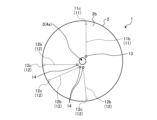
- FIG. 14 and 15 are front views showing an example of the configuration of a flow path structure 1 according to a third modification of the embodiment. Note that FIG. 14 is a front view when viewed from the first surface 2a side of the base body 2, and FIG. 15 is a front view when viewed from the second surface 2b side of the base body 2.
- thermocouple sections 10 As shown in FIGS. 14 and 15, in Modification 3, a plurality of thermocouple sections 10, three in the figure, are connected to the second surface 2b through the wiring section 11b and via section 11c of the common first metal wiring 11. It is connected to one terminal 13 located at.
- thermocouple sections 10 are respectively connected to the plurality of terminals 14 located on the second surface 2b via the wiring section 12b and the via section 12c of the individual second metal wiring 12. Ru.
- the manufacturing process of the flow path structure 1 can be simplified.
- each thermocouple section 10 can be measured by switching the terminal 14 to be measured with a temperature measuring device (not shown).
- FIGS. 13 and 14 show examples in which the first metal wiring 11 is shared, the present disclosure is not limited to such examples, and the second metal wiring 12 may be shared. That is, either the first metal wiring 11 or the second metal wiring 12 may be shared.
- FIGS. 13 and 14 show examples in which the via portions 11c and 12c are located at the peripheral edge of the base 2, the present disclosure is not limited to such examples.
- the via portions 11c and 12c may be located on the support. Thereby, the degree of freedom in designing the first metal wiring 11 and the second metal wiring 12 can be improved.
- FIG. 16 is a front view showing an example of the configuration of a flow path structure 1 according to a fourth modification of the embodiment.
- the thermocouple section 10 when the first surface 2a is viewed from the front, the thermocouple section 10 is further away from the center of the first surface 2a than the aperture group 5A composed of the plurality of apertures 5. It may be located at any position.
- thermocouple section 10 outside the opening group 5A, it is possible to measure the temperature outside the opening group 5A, where the temperature tends to drop during the process.
- FIG. 17 is an enlarged cross-sectional view showing an example of the configuration of a flow path structure 1 according to modification 5 of the embodiment. Note that FIG. 17 is an enlarged cross-sectional view of the peripheral portion of the base body 2. As shown in FIG. As shown in FIG. 17, in modification 5, the RF electrode 20 is located inside the base 2 along the first surface 2a.
- the RF electrode 20 is connected to a high frequency power source (not shown). Then, by applying a high frequency to the RF electrode 20 from such a high frequency power source, plasma can be generated inside the semiconductor manufacturing apparatus 100 (see FIG. 1).
- thermocouple section 10 is located further away from the center of the first surface 2a than the RF electrode 20. Good too.
- thermocouple section 10 is located outside the RF electrode 20, when generating plasma on the first surface 2a side of the base body 2, the thermocouple section 10 of the conductive material It is possible to reduce the possibility that the transmission of high frequency waves toward the surface 2a is inhibited.
- FIG. 18 is an enlarged sectional view showing an example of the configuration of a flow path structure 1 according to modification 6 of the embodiment. As shown in FIG. 18, the thermocouple section 10 may be located further away from the first surface 2a than the RF electrode 20.
- thermocouple section 10 is located farther away from the first surface 2a than the RF electrode 20, so that when generating plasma on the first surface 2a side of the base 2, the thermocouple section of the conductor 10 can reduce the possibility that the transmission of high frequency waves toward the first surface 2a side of the base body 2 is inhibited.
- the flow path structure 1 includes a base 2, a flow path 4, a plurality of openings 5, a first metal wiring 11, and a second metal wiring 12.
- the base body 2 has a first surface 2a and is made of ceramics.
- the flow path 4 is located inside the base 2 and has a plurality of branch paths 4c.
- the plurality of openings 5 are located on the first surface 2a and are respectively connected to the plurality of branch paths 4c.
- the first metal wiring 11 is at least partially located inside the base 2 and is made of a first metal.
- the second metal wiring 12 is at least partially located inside the base 2 and is made of a second metal different from the first metal.
- first metal wiring 11 and the second metal wiring 12 are connected inside the base 2 and constitute a thermocouple section 10 having a thermocouple function.
- first metal wiring 11 and the second metal wiring 12 surround the opening 5, and the thermocouple section 10 is located around the opening 5. Thereby, process data during the process can be estimated with high accuracy.
- thermocouple section 10 surrounds the opening 5 when the first surface 2a is viewed from the front. Therefore, process data during the process can be estimated with higher accuracy.
- thermocouple section 10 when the first surface 2a is viewed from the front, the first metal wiring 11 and the second metal wiring 12 are located in an overlapping position in the thermocouple section 10. Thereby, process data during the process can be estimated with higher accuracy.
- thermocouple section 10 has a region containing the first metal and the second metal. Therefore, the reliability of the thermocouple section 10 can be improved.
- thermocouple section 10 when the first surface 2a is viewed from the front, the thermocouple section 10 is located closer to the center of the first surface 2a than the opening group 5A constituted by the plurality of openings 5. located in a remote location. Thereby, process data during the process can be estimated with high accuracy.
- the base body 2 further includes an RF electrode 20 located inside. Furthermore, when the first surface 2a is viewed from the front, the thermocouple section 10 is located further away from the center of the first surface 2a than the RF electrode 20 is. Thereby, process data during the process can be estimated with high accuracy, and the process of the semiconductor wafer W in the semiconductor manufacturing apparatus 100 can be carried out stably.
- the base body 2 further includes an RF electrode 20 located inside. Furthermore, the thermocouple section 10 is located further away from the first surface 2a than the RF electrode 20 is. Thereby, process data during the process can be estimated with high accuracy, and the process of the semiconductor wafer W in the semiconductor manufacturing apparatus 100 can be carried out stably.
- the semiconductor manufacturing apparatus 100 includes a mounting table 120, a chamber 110, and the flow path structure 1 described above. Thereby, the semiconductor wafer W can be processed while accurately estimating the process data during the process.
- a heater may be provided inside the base body 2 in the flow path structure 1 of the present disclosure. Thereby, the process gas flowing through the flow path 4 can be heated. Further, the temperature of the heater can also be measured by the thermocouple section 10. In the present disclosure, by using the thermocouple section 10, local temperature measurement is possible, and by having a plurality of thermocouple sections 10, the temperature distribution within the shower plate can be precisely measured.
Landscapes
- Chemical & Material Sciences (AREA)
- Physics & Mathematics (AREA)
- Engineering & Computer Science (AREA)
- Plasma & Fusion (AREA)
- Analytical Chemistry (AREA)
- General Physics & Mathematics (AREA)
- Chemical Kinetics & Catalysis (AREA)
- Materials Engineering (AREA)
- Mechanical Engineering (AREA)
- Metallurgy (AREA)
- Organic Chemistry (AREA)
- General Chemical & Material Sciences (AREA)
- Measuring Temperature Or Quantity Of Heat (AREA)
Priority Applications (3)
| Application Number | Priority Date | Filing Date | Title |
|---|---|---|---|
| KR1020247031381A KR20240152374A (ko) | 2022-03-29 | 2023-03-29 | 유로 구조체 및 반도체 제조 장치 |
| JP2024512744A JP7780003B2 (ja) | 2022-03-29 | 2023-03-29 | 流路構造体および半導体製造装置 |
| US18/849,387 US20250201600A1 (en) | 2022-03-29 | 2023-03-29 | Channel structure and semiconductor manufacturing device |
Applications Claiming Priority (2)
| Application Number | Priority Date | Filing Date | Title |
|---|---|---|---|
| JP2022054592 | 2022-03-29 | ||
| JP2022-054592 | 2022-03-29 |
Publications (1)
| Publication Number | Publication Date |
|---|---|
| WO2023190786A1 true WO2023190786A1 (ja) | 2023-10-05 |
Family
ID=88202631
Family Applications (1)
| Application Number | Title | Priority Date | Filing Date |
|---|---|---|---|
| PCT/JP2023/013014 Ceased WO2023190786A1 (ja) | 2022-03-29 | 2023-03-29 | 流路構造体および半導体製造装置 |
Country Status (4)
| Country | Link |
|---|---|
| US (1) | US20250201600A1 (https=) |
| JP (1) | JP7780003B2 (https=) |
| KR (1) | KR20240152374A (https=) |
| WO (1) | WO2023190786A1 (https=) |
Citations (4)
| Publication number | Priority date | Publication date | Assignee | Title |
|---|---|---|---|---|
| JP2002327274A (ja) * | 2001-02-09 | 2002-11-15 | Tokyo Electron Ltd | 成膜装置 |
| US20190040529A1 (en) * | 2017-08-04 | 2019-02-07 | Asm Ip Holding B.V. | Showerhead assembly for distributing a gas within a reaction chamber and a method for controlling the temperature uniformity of a showerhead assembly |
| JP2019220593A (ja) * | 2018-06-20 | 2019-12-26 | 新光電気工業株式会社 | 静電チャック、基板固定装置 |
| JP2021176192A (ja) * | 2020-04-22 | 2021-11-04 | 京セラ株式会社 | 流路構造体および半導体製造装置 |
Family Cites Families (1)
| Publication number | Priority date | Publication date | Assignee | Title |
|---|---|---|---|---|
| JP7458808B2 (ja) | 2020-02-07 | 2024-04-01 | 東京エレクトロン株式会社 | プロセス推定システム、プロセスデータ推定方法及びプログラム |
-
2023
- 2023-03-29 JP JP2024512744A patent/JP7780003B2/ja active Active
- 2023-03-29 KR KR1020247031381A patent/KR20240152374A/ko active Pending
- 2023-03-29 WO PCT/JP2023/013014 patent/WO2023190786A1/ja not_active Ceased
- 2023-03-29 US US18/849,387 patent/US20250201600A1/en active Pending
Patent Citations (4)
| Publication number | Priority date | Publication date | Assignee | Title |
|---|---|---|---|---|
| JP2002327274A (ja) * | 2001-02-09 | 2002-11-15 | Tokyo Electron Ltd | 成膜装置 |
| US20190040529A1 (en) * | 2017-08-04 | 2019-02-07 | Asm Ip Holding B.V. | Showerhead assembly for distributing a gas within a reaction chamber and a method for controlling the temperature uniformity of a showerhead assembly |
| JP2019220593A (ja) * | 2018-06-20 | 2019-12-26 | 新光電気工業株式会社 | 静電チャック、基板固定装置 |
| JP2021176192A (ja) * | 2020-04-22 | 2021-11-04 | 京セラ株式会社 | 流路構造体および半導体製造装置 |
Also Published As
| Publication number | Publication date |
|---|---|
| JP7780003B2 (ja) | 2025-12-03 |
| US20250201600A1 (en) | 2025-06-19 |
| KR20240152374A (ko) | 2024-10-21 |
| JPWO2023190786A1 (https=) | 2023-10-05 |
Similar Documents
| Publication | Publication Date | Title |
|---|---|---|
| JP2980688B2 (ja) | 還元又は酸化ガス用のガスセンサ | |
| KR102780233B1 (ko) | 정전 척 및 기판 고정 장치 | |
| US6081182A (en) | Temperature sensor element and temperature sensor including the same | |
| US20030203225A1 (en) | Aluminum nitride sintered body, ceramic substrate, ceramic heater and electrostatic chuck | |
| US20060191879A1 (en) | Plasma processing member | |
| US20200404747A1 (en) | Holding device and method of manufacturing holding device | |
| EP2360482B1 (en) | Base member for probe unit, and probe unit | |
| US20030122453A1 (en) | Elastic wave element and method for fabricating the same | |
| JP7213656B2 (ja) | 保持装置 | |
| WO2001006559A1 (fr) | Testeur de tranche | |
| WO2023190786A1 (ja) | 流路構造体および半導体製造装置 | |
| WO2023190785A1 (ja) | 流路構造体および半導体製造装置 | |
| JP7772634B2 (ja) | 流路構造体および半導体製造装置 | |
| TW202044463A (zh) | 溫度調節單元 | |
| KR20210116654A (ko) | 개선된 고온 칩 | |
| WO2017188377A1 (ja) | 試料搬送部材 | |
| JP2002025912A (ja) | 半導体製造装置用サセプタとそれを用いた半導体製造装置 | |
| US8240650B2 (en) | Chuck with triaxial construction | |
| TWI735364B (zh) | 靜電吸盤 | |
| CN120199673A (zh) | 陶瓷基座 | |
| CN113207199A (zh) | 陶瓷加热器 | |
| WO2007021350A2 (en) | Method and apparatus for monitoring thickness of conductive coating | |
| JP7198635B2 (ja) | 保持装置 | |
| KR102842210B1 (ko) | 기판 처리 장치 | |
| TWI792837B (zh) | 多層結構及其製造方法 |
Legal Events
| Date | Code | Title | Description |
|---|---|---|---|
| 121 | Ep: the epo has been informed by wipo that ep was designated in this application |
Ref document number: 23780794 Country of ref document: EP Kind code of ref document: A1 |
|
| ENP | Entry into the national phase |
Ref document number: 2024512744 Country of ref document: JP Kind code of ref document: A |
|
| ENP | Entry into the national phase |
Ref document number: 20247031381 Country of ref document: KR Kind code of ref document: A |
|
| WWE | Wipo information: entry into national phase |
Ref document number: 18849387 Country of ref document: US Ref document number: 1020247031381 Country of ref document: KR |
|
| NENP | Non-entry into the national phase |
Ref country code: DE |
|
| 122 | Ep: pct application non-entry in european phase |
Ref document number: 23780794 Country of ref document: EP Kind code of ref document: A1 |
|
| WWP | Wipo information: published in national office |
Ref document number: 18849387 Country of ref document: US |