WO2023188555A1 - 固体電解コンデンサ、および固体電解コンデンサの製造方法 - Google Patents
固体電解コンデンサ、および固体電解コンデンサの製造方法 Download PDFInfo
- Publication number
- WO2023188555A1 WO2023188555A1 PCT/JP2022/045256 JP2022045256W WO2023188555A1 WO 2023188555 A1 WO2023188555 A1 WO 2023188555A1 JP 2022045256 W JP2022045256 W JP 2022045256W WO 2023188555 A1 WO2023188555 A1 WO 2023188555A1
- Authority
- WO
- WIPO (PCT)
- Prior art keywords
- dam
- solid electrolytic
- flat film
- capacitor element
- forming
- Prior art date
- Legal status (The legal status is an assumption and is not a legal conclusion. Google has not performed a legal analysis and makes no representation as to the accuracy of the status listed.)
- Ceased
Links
Images







Classifications
-
- H—ELECTRICITY
- H01—ELECTRIC ELEMENTS
- H01G—CAPACITORS; CAPACITORS, RECTIFIERS, DETECTORS, SWITCHING DEVICES, LIGHT-SENSITIVE OR TEMPERATURE-SENSITIVE DEVICES OF THE ELECTROLYTIC TYPE
- H01G9/00—Electrolytic capacitors, rectifiers, detectors, switching devices, light-sensitive or temperature-sensitive devices; Processes of their manufacture
- H01G9/004—Details
- H01G9/008—Terminals
- H01G9/012—Terminals specially adapted for solid capacitors
-
- H—ELECTRICITY
- H01—ELECTRIC ELEMENTS
- H01G—CAPACITORS; CAPACITORS, RECTIFIERS, DETECTORS, SWITCHING DEVICES, LIGHT-SENSITIVE OR TEMPERATURE-SENSITIVE DEVICES OF THE ELECTROLYTIC TYPE
- H01G9/00—Electrolytic capacitors, rectifiers, detectors, switching devices, light-sensitive or temperature-sensitive devices; Processes of their manufacture
- H01G9/004—Details
- H01G9/04—Electrodes or formation of dielectric layers thereon
- H01G9/048—Electrodes or formation of dielectric layers thereon characterised by their structure
-
- H—ELECTRICITY
- H01—ELECTRIC ELEMENTS
- H01G—CAPACITORS; CAPACITORS, RECTIFIERS, DETECTORS, SWITCHING DEVICES, LIGHT-SENSITIVE OR TEMPERATURE-SENSITIVE DEVICES OF THE ELECTROLYTIC TYPE
- H01G9/00—Electrolytic capacitors, rectifiers, detectors, switching devices, light-sensitive or temperature-sensitive devices; Processes of their manufacture
- H01G9/15—Solid electrolytic capacitors
Definitions
- the present invention relates to a solid electrolytic capacitor having a structure in which a laminate of a plurality of capacitor elements is molded with an insulating resin.
- Patent Document 1 describes a method for manufacturing a solid electrolytic capacitor and a solid electrolytic capacitor.
- the solid electrolytic capacitor described in Patent Document 1 includes a plurality of flat film capacitor elements and a plurality of metal foils (cathode).
- a flat film capacitor element includes a foil-like valve metal base, a porous portion and a dielectric layer formed on the surface of the valve metal base, and a solid electrolyte layer formed on the surface of the dielectric layer.
- a mask layer is formed on the surface of the dielectric layer in Patent Document 1 to cover the ends and sides of each element region.
- a solid electrolyte layer is formed in a region surrounded by this mask layer.
- an insulating adhesive layer is formed so as to overlap this mask layer, and a conductive layer is formed on this solid electrolyte layer.
- the flat film-shaped capacitor elements and metal foils thus formed are alternately laminated, thereby forming an element laminate.
- the element stack is sealed with an insulating resin.
- Patent Document 2 describes a surface-mount thin capacitor.
- the cathode portion of the surface-mount thin capacitor described in Patent Document 2 is formed by laminating a conductive polymer, a graphite layer, and a silver paste layer on the surface of an anode (aluminum foil).
- a resist resin is formed at the boundary between the anode (aluminum foil) and the cathode.
- An insulating resin is formed so as to partially cover this resist resin.
- Patent Document 2 On the other hand, in the surface mount thin capacitor shown in Patent Document 2, as described above, an insulating resin is formed so as to cover a part of the resist resin formed at the boundary between the anode and cathode parts. However, since the insulating resin only covers a part of the resist resin, when re-forming is performed, the resist resin and conductive polymer will shrink, and the chemical solution will flow between the resist resin and the conductive polymer. Get into it. This creates a gap between the resist resin and the conductive polymer. Therefore, the configuration of Patent Document 2 may also cause the same problem as Patent Document 1.
- an object of the present invention is to provide a solid electrolytic capacitor that can suppress short circuits between an anode and a cathode and achieve high reliability.
- the solid electrolytic capacitor of the present invention includes a sheet laminate formed by alternately laminating a plurality of flat film capacitor elements and a plurality of flat film cathode electrode foils via a conductive adhesive; and an insulating resin that seals the laminate.
- a flat film capacitor element includes a flat film-like anode electrode foil, a dielectric layer formed on the surface of the anode electrode foil, a first dam formed on the surface of the dielectric layer, and a first dam.
- a solid electrolyte layer formed within a region regulated by.
- the conductive adhesive is formed within a region regulated by the second dam that overlaps at least the first dam.
- the second dam is formed to cover the boundary between the solid electrolyte layer and the first dam.
- an object of the present invention is to provide a solid electrolytic capacitor that can suppress short circuits between an anode and a cathode and achieve high reliability.
- FIG. 1 is a side sectional view showing the configuration of a solid electrolytic capacitor according to a first embodiment.
- FIG. 2(A) is a side cross-sectional view showing the configuration of a set of a capacitor element and a cathode electrode before singulation
- FIG. 2(B) is a side cross-sectional view showing the configuration of the capacitor element before singulation.
- FIG. 2C is a side cross-sectional view showing the configuration of a set of a capacitor element and a cathode electrode after being separated into pieces.
- FIG. 3(A) is a diagram schematically showing the structure of the capacitor element and cathode electrode of the present invention, and FIG.
- FIG. 3(B) is a diagram schematically showing the structure of the capacitor element and cathode electrode of the conventional configuration.
- FIG. FIG. 4(A) is a plan view schematically showing the structure of the capacitor element and cathode electrode of the present invention
- FIG. 4(B) is a plan view schematically showing the structure of the capacitor element and cathode electrode of the conventional configuration.
- FIG. FIG. 5 is a flowchart showing an example of a schematic flow of the method for manufacturing a solid electrolytic capacitor according to the present embodiment.
- FIG. 6 is a flowchart showing an example of a process for forming a capacitor element sheet.
- FIG. 7(A) is an external perspective view showing the shape of the anode electrode and dielectric layer of the capacitor element before singulation, and FIG.
- FIG. 7(B) is an external appearance showing the shape of the capacitor element before singulation.
- FIG. FIG. 8 is an external view in the multi-state.
- FIG. 9 is an external perspective view showing the shape of the cathode electrode before singulation.
- FIG. 10 is a flowchart illustrating an example of a process for forming a sheet laminate.
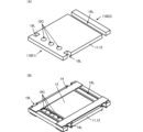
- FIGS. 11(A) and 11(B) are external perspective views showing a state in which a second dam is formed on the capacitor element sheet.
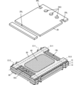
- 12(A) and 12(B) are external perspective views showing a state in which a second dam and an adhesive are formed on a capacitor element sheet.
- 13(A) and 13(B) are exploded perspective views showing a state in which a capacitor element sheet and a cathode electrode sheet are laminated.
- FIG. 11(A) and 11(B) are external perspective views showing a state in which a second dam is formed on the capacitor element sheet.
- 12(A) and 12(B) are external perspective views showing
- FIG. 14(A) is an exploded perspective view showing a laminated state of a capacitor element sheet and a cathode electrode sheet in a multi-state
- FIG. 14(B) is an exploded perspective view showing a laminated state of a capacitor element sheet and a cathode electrode sheet in a multi-state
- FIG. 3 is an external perspective view showing a stacked state
- FIG. 15 is an exploded perspective view showing the state of the capacitor element sheet and the cathode electrode sheet in a multi-state state.
- FIG. 16(A) is a side cross-sectional view showing the configuration of a set of a capacitor element and a cathode electrode before singulation in the second embodiment
- FIG. 1 is a side sectional view showing the configuration of a solid electrolytic capacitor according to a first embodiment. Note that in FIG. 1, only the insulating resin and the external electrodes are hatched to make the diagram easier to read.
- FIG. 2(A) is a side sectional view showing the configuration of a set of a capacitor element and a cathode electrode before being separated into pieces.
- FIG. 2(B) is a side cross-sectional view showing the structure of the capacitor element before being separated into pieces.
- FIG. 2(C) is a side sectional view showing the configuration of a set of a capacitor element and a cathode electrode after being separated into pieces.
- the solid electrolytic capacitor 1 includes a capacitor element laminate 100, an insulating resin 50, an external electrode 61, and an external electrode. 62.
- the capacitor element laminate 100 includes a plurality of flat film-shaped capacitor elements 10 , a plurality of flat film-shaped cathode electrodes 20 , a second dam 30 , and an adhesive 40 .
- the number of flat film capacitor elements 10 and the number of cathode electrodes is four, but the number is not limited to this.
- the cathode electrode 20 corresponds to the "cathode electrode foil" in the present invention.
- the side sectional views in FIGS. 1, 2(A), 2(B), and 2(C) are sectional views taken along a plane perpendicular to the top surface 101 and bottom surface 102 of the capacitor element laminate 100 in FIG. .
- the capacitor element 10 includes a flat film-shaped anode electrode 11, a dielectric layer 12, and a CP layer (solid electrolyte layer) 13.
- the anode electrode 11 includes a large number of holes. In other words, the anode electrode 11 is in a porous state (porous body). The ratio of the thicknesses of the porous portion and core metal portion on one side of the anode electrode 11 to the porous portion on the other side is approximately 1:1:1.
- Dielectric layer 12 covers the outer surface of anode electrode 11 . Since the detailed structure of the anode electrode 11 is not shown in FIG. 2, the dielectric layer 12 is schematically shown covering the macroscopic surface of the anode electrode 11. In reality, the dielectric layer 12 covers not only the macroscopic surface of the anode electrode 11 but also the surfaces of many holes in the anode electrode 11 . Note that the anode electrode 11 corresponds to the "anode electrode foil" in the present invention.
- the CP layer 13 covers the surface of the dielectric layer 12.
- the CP layer 13 is formed inside a frame-shaped first dam 14.
- the first dam 14 has insulation properties.
- the region in which the CP layer 13 is formed is regulated by the first dam 14 .
- the first dam 14 may not be formed in a frame shape. That is, the first dam 14 may be formed on one side, or may be formed on two sides having corners. Furthermore, the structure may be formed on two opposing sides in a plan view.
- the CP layer 13 has a laminated structure of an inner layer CP (inner solid electrolyte layer) 131 and an outer layer CP (outer solid electrolyte layer) 132.
- the inner layer CP131 is formed on the surface of the dielectric layer 12, and the outer layer CP132 is formed on the surface of the inner layer CP131.
- the plurality of capacitor elements 10 and the plurality of cathode electrodes 20 are alternately stacked so that their flat film surfaces are parallel and overlap in plan view.
- a second dam 30 and an adhesive 40 are provided between adjacent capacitor elements 10 and cathode electrodes 20.
- the second dam 30 has insulation properties.
- Adhesive 40 has electrical conductivity. Note that the adhesive 40 corresponds to the "conductive adhesive" in the present invention.
- the second dam 30 has a frame shape.
- the adhesive 40 is placed inside the frame defined by the second dam 30. Adjacent capacitor elements 10 and cathode electrodes 20 are bonded together by this adhesive 40 .
- the second dam 30 is formed to overlap the outer layer CP 132. In other words, it is formed to cover the end of the first dam 14 and the end of the outer layer CP132. A more detailed structure will be described later.
- the second dam 30 is made of an insulating material such as an insulating resin, for example.
- the second dam 30 has a dam adjustment section 30L.
- This dam adjustment section 30L is used to control the volume when applying the second dam 30.
- unnecessary expansion of the second dam 30 during stacking is suppressed.
- the second dam 30 enters, for example, the anode through holes 19C and 19L and the cathode through holes 29C and 29L (detailed configurations of which are shown below).
- the dam adjustment portion 30L it is possible to inhibit molding by the insulating resin 50 and prevent molding defects from occurring.
- the dam adjustment section 30L is formed by a printed pattern.
- the dam adjustment portion 30L may be a through hole or may have a shape having a bottom surface on the second dam 30 like a recessed portion. Further, it is preferable to form the size (width, length) of the dam adjustment portion 30L according to the volume of the second dam 30.
- the second dam 30 is expanded by heating and pressurizing the capacitor element 10 and the cathode electrode 20. This reduces the difference in thickness between the dam adjustment portion 30L and other portions.
- the first ends 10E1 (see FIG. 2C) of the plurality of capacitor elements 10 are at approximately the same position when viewed from the side.
- the second ends 10E2 (see FIG. 2C) of the plurality of capacitor elements 10 are at substantially the same position when viewed from the side.
- the first ends 20E1 (see FIG. 2C) of the plurality of cathode electrodes 20 are at substantially the same position when viewed from the side.
- the second ends 20E2 (see FIG. 2C) of the plurality of cathode electrodes 20 are at substantially the same position when viewed from the side.
- the first ends 10E1 of the plurality of capacitor elements 10 and the second ends 20E2 of the plurality of cathode electrodes 20 are arranged on the first end side of the capacitor element stack 100.
- the first ends 10E1 of the plurality of capacitor elements 10 protrude further outward than the second ends 20E2 of the plurality of cathode electrodes 20.
- the second ends 10E2 of the plurality of capacitor elements 10 and the first ends 20E1 of the plurality of cathode electrodes 20 are arranged on the second end side of the capacitor element stack 100.
- the first ends 20E1 of the plurality of cathode electrodes 20 protrude further outward than the second ends 10E2 of the plurality of capacitor elements 10.
- the capacitor element stack 100 is realized.
- the capacitor element stack 100 is sealed with an insulating resin 50. More specifically, the insulating resin 50 is applied to the capacitor element laminate except for the first ends 10E1 of the plurality of capacitor elements 10 (the first ends 10E1 of the anode electrodes 11) and the first ends 20E1 of the plurality of cathode electrodes 20. Cover 100.
- the external electrode 61 covers the first end of the insulating resin 50 (the first end 10E1 of the anode electrode 11).
- the external electrode 61 is connected to the first end 10E1 of the anode electrode 11 of the plurality of capacitor elements 10.
- the external electrode 62 covers the second end of the insulating resin 50 (the first end 20E1 of the cathode electrode 20).
- the external electrode 62 is connected to the first end 20E1 of the plurality of cathode electrodes 20.
- the solid electrolytic capacitor 1 is realized.
- FIG. 3(A) is a side sectional view schematically showing the structure of the capacitor element 10 and the cathode electrode 20, and is an enlarged view of the structure of FIG. 2(A) described above.
- FIG. 3(B) is a side sectional view schematically showing the structure of the capacitor element 10 and the cathode electrode 20 according to the conventional structure.
- FIGS. 3(A) is a side sectional view schematically showing the structure of the capacitor element 10 and the cathode electrode 20 according to the conventional structure.
- FIGS. 3A and 3B are cross-sectional views taken along a plane perpendicular to the top surface 101 and bottom surface 102 of the capacitor element laminate 100 in FIG.
- FIGS. 3A and 3B show only one set of the capacitor element 10 and the cathode electrode 20, the solid electrolytic capacitor 1 is formed by laminating a plurality of these sets.
- an outer layer CP 132 is formed within the region surrounded by the first dam 14.
- a boundary portion BD exists at the boundary between the inside of the area formed by the first dam 14 and the area where the outer layer CP132 is formed. Due to the existence of this boundary portion BD, the dielectric layer 12 is exposed. For convenience, the boundary portion BD and the exposed portion of the dielectric layer 12 are shown as the same portion.
- the second dam 30 is formed to cover this boundary portion BD. That is, even if the dielectric layer 12 is exposed, the second dam 30 enters the exposed portion. Therefore, the dielectric layer 12 is not exposed.
- FIG. 4(A) is a plan view schematically showing the arrangement of the adhesive 40 on the capacitor element 10.
- FIG. 4(B) is a plan view schematically showing the arrangement of the adhesive 40 on the capacitor element 10 in a conventional configuration. Note that in FIGS. 4(A) and 4(B), in order to explain the dielectric layer 12 in an easy-to-understand manner, the hatching is different from that in other figures, and each structure is The composition is expanded and exaggerated.
- the positional relationship between the inner circumferential portion 14P of the first dam 14 and the inner circumferential portion 30P of the second dam 30 is compared.
- the inner peripheral part 30P is formed inside the capacitor element 10 (inner side in plan view) at a distance d from the inner peripheral part 14P over the entire circumference. That is, the second dam 30 is formed to extend further into the capacitor element 10 than the first dam 14 at the distance d.
- the distance d is preferably in a range of about 50 ⁇ m to about 100 ⁇ m.
- the boundary portion BD is covered by the second dam 30. That is, even if the adhesive 40 wets and spreads through a process such as heating and pressing, the adhesive 40 does not come into contact with the dielectric layer 12 (boundary portion BD). That is, short circuit between the anode electrode 11 and the cathode electrode 20 can be suppressed.
- FIG. 5 is a flowchart showing an example of a schematic flow of the method for manufacturing a solid electrolytic capacitor according to the present embodiment.
- a capacitor element sheet is formed (FIG. 5: S11).
- a plurality of capacitor elements 10 forming different solid electrolytic capacitors 1 are arranged on the capacitor element sheet.
- the capacitor element sheet and the cathode electrode sheet are laminated with the adhesive 40 in between to form a sheet laminate (FIG. 5: S12).
- a plurality of cathode electrodes 20 forming different solid electrolytic capacitors 1 are arranged in the cathode electrode sheet.
- a structure in which a plurality of capacitor element laminates 100 are arranged in a plane is formed.
- the sheet laminate is one in which a plurality of capacitor element laminates 100 are arranged in a plane.
- the sheet stack is sealed with insulating resin 50 (FIG. 5: S13). Although details will be described later, at this time, a through hole penetrating from the upper surface to the lower surface of the sheet laminate is provided in the sheet laminate, and resin sealing is performed by compression molding.
- This sealing with the insulating resin 50 is performed in a multi-state state (a state in which a plurality of solid electrolytic capacitors 1 are arranged) before the solid electrolytic capacitors 1 are separated into individual pieces.
- the sheet stack sealed with the insulating resin 50 is cut into individual pieces (FIG. 5: S14). Specifically, cutting is performed along cutting lines E11, E12, S11, and S12 shown in FIG. 13(B), which will be described later. As a result, a plurality of solid electrolytic capacitors 1 (referred to as elements of solid electrolytic capacitors 1) in which no external electrodes are formed are formed. Thereafter, the element body of the solid electrolytic capacitor 1 is subjected to secondary sealing with an insulating resin 50.
- the side surface of the element body of the solid electrolytic capacitor 1 (the surface cut along the cutting lines S11 and S12 (the top surface, the bottom surface, the side surface different from the end surface where the anode electrode 11 and the cathode electrode 20 are exposed)) is insulated. It is covered by secondary sealing with a synthetic resin 50. Thereby, the anode electrode 11 and the cathode electrode 20 that are unnecessarily exposed during singulation are covered with the insulating resin 50.
- external electrodes 61 and 62 are formed on the end face of the element body of solid electrolytic capacitor 1 (FIG. 5: S15).
- FIG. 6 is a flowchart showing an example of a process for forming a capacitor element sheet.
- FIG. 7(A) is an external perspective view showing the shape of the anode electrode and dielectric layer of the capacitor element before singulation
- FIG. 7(B) is an external appearance showing the shape of the capacitor element before singulation.
- FIG. 8 is an external view in the multi-state.
- a chemical conversion treatment is performed on the anode electrode 11 to form the dielectric layer 12 (FIG. 6: S111).
- a large number of holes are formed on the surface of the anode electrode 11 by etching, and the vicinity of the surface of the anode electrode 11 is a porous body.
- the dielectric layer 12 covers the surface of the anode electrode 11 including the inner surface of the hole.
- an anode through hole is formed in the anode electrode 11 (FIG. 6: S112). More specifically, as shown in FIG. 7A, a plurality of cylindrical anode through holes 19C and groove-shaped anode through holes 19L are formed in the anode electrode 11.
- the plurality of cylindrical anode through-holes 19C and the groove-shaped anode through-holes 19L are arranged alternately along the direction in which the portions that will become the plurality of anode electrodes 11 are lined up.
- the plurality of cylindrical anode through holes 19C are formed at positions that realize the first ends 10E1 of the anode electrodes 11, and the groove-shaped anode through holes 19L are formed at positions that straddle the portions that will become adjacent anode electrodes 11. And, it is formed at a position that realizes the second end 10E2 of the adjacent anode electrodes 11.
- a CP layer (solid electrolyte layer) 13 is formed on the surface of the dielectric layer 12 (FIG. 6: S113). More specifically, as shown in FIG. 7(B), a first dam 14 having a frame-shaped opening is formed. Then, the CP layer 13 (a laminated structure of the inner layer CP131 and the outer layer CP132) is formed in the opening of the first dam 14.
- this structure has a multi-state structure in which a plurality of capacitor elements 10 (a structure consisting of an anode electrode 11, a dielectric layer 12, a CP layer 13, and a first dam 14) are arranged in two dimensions. It will be held in
- FIG. 9 is an external perspective view showing the shape of the cathode electrode before singulation.
- the cathode electrode 20 is formed with a plurality of cylindrical cathode through holes 29C and groove-shaped cathode through holes 29L.
- the plurality of cylindrical cathode through-holes 29C and the groove-shaped cathode through-holes 29L are arranged alternately along the direction in which the portions that will become the plurality of cathode electrodes 20 are lined up.
- the plurality of cylindrical cathode through holes 29C are formed at positions that realize the first ends 20E1 of the cathode electrodes 20, and the groove-shaped cathode through holes 29L are formed at positions that straddle the portions that will become adjacent cathode electrodes 20, And, it is formed at a position that realizes the second end 20E2 of the adjacent cathode electrodes 20.
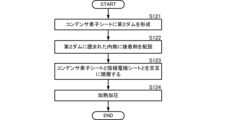
- FIG. 10 is a flowchart illustrating an example of a process for forming a sheet laminate.
- FIG. 11 is an external perspective view showing a state in which a second dam is formed on a capacitor element sheet
- FIG. 11(A) shows a multi-state state
- FIG. 11(B) shows a portion of one capacitor element.
- FIG. 12 is an external perspective view showing a state in which a second dam and adhesive are formed on a capacitor element sheet
- FIG. 12(A) shows a multi-layer state
- FIG. 12(B) shows a portion of one capacitor element.
- shows. 13(A) and 13(B) are exploded perspective views showing a state in which a capacitor element sheet and a cathode electrode sheet are laminated.
- FIG. 14(A) is an exploded perspective view showing a laminated state of a capacitor element sheet and a cathode electrode sheet in a multi-state
- FIG. 14(B) is an exploded perspective view showing a laminated state of a capacitor element sheet and a cathode electrode sheet in a multi-state
- FIG. 3 is an external perspective view showing a stacked state
- FIG. 15 is a diagram showing the structure after laminating a capacitor element sheet and a cathode electrode sheet and heating and pressurizing them.
- a second dam 30 is formed on the sheet stack (FIG. 10: S121). More specifically, as shown in FIGS. 11(A) and 11(B), a second dam 30 having a frame-shaped opening is formed. The second dam 30 is formed at a position overlapping the first dam 14. Furthermore, the second dam 30 is formed to an area inside the inner frame of the first dam 14.
- the shape at the time of printing is not limited to this, as long as the second dam 30 has a shape that expands further inward than the inner frame of the first dam 14 during heating and pressurization, which will be described later.
- the second dam 30 is formed by a printed pattern so as to have a dam adjustment portion 30L.
- FIG. 11(A) the example in which the dam adjustment part 30L is formed in the whole 1st dam 14 was shown.
- a configuration may be adopted in which the dam adjustment portion 30L is not formed over the entire first dam 14. That is, the number of dam adjustment parts 30L may be formed according to the volume of the adhesive 40, similar to the size of the dam adjustment parts 30L described above.
- the adhesive 40 is placed inside the opening of the second dam 30 (FIG. 10: S122).
- capacitor element sheets and cathode electrode sheets are alternately laminated (FIG. 10: S123) . More specifically, the capacitor element sheet and the cathode electrode sheet are laminated so as to satisfy the following conditions.
- the plurality of cylindrical anode through holes 19C in the capacitor element sheet and the groove-shaped cathode through holes 29L in the cathode electrode sheet overlap.
- the groove-shaped anode through-hole 19L in the capacitor element sheet overlaps with the plurality of cylindrical cathode through-holes 29C in the cathode electrode sheet.
- the groove-shaped anode through-hole 19L in the capacitor element sheet and the groove-shaped cathode through-hole 29L in the cathode electrode sheet overlap.
- a plurality of these through holes are formed in accordance with the number of capacitor elements arranged in the sheet laminate. Therefore, a plurality of through holes are formed in the sheet stack, which penetrate from the top surface to the bottom surface of the sheet stack.
- the sheet laminate is heated and pressurized (FIG. 10: S124). Thereby, the capacitor element sheet and the cathode electrode sheet are adhered by the adhesive 40, and a sheet laminate is formed. As shown in FIG. 15, this heating and pressing causes the adhesive 40 to spread in a plane. However, since the second dam 30 covers the boundary portion BD, contact between the adhesive 40 and the anode electrode 11 can be suppressed. That is, short circuit between the anode and the cathode is suppressed.
- the dam adjustment portion 30L formed in the second dam 30 is closed. Therefore, the thickness of the second dam 30 can be adjusted, and the thickness of the second dam 30 can be prevented from becoming unnecessarily high. Therefore, the height of the sheet laminate can be reduced.
- FIG. 16(A) is a side cross-sectional view showing the configuration of a set of a capacitor element and a cathode electrode before singulation in the second embodiment, and FIG. FIG.
- the solid electrolytic capacitor 1A according to the second embodiment has a third electrode on the cathode electrode 20A, unlike the solid electrolytic capacitor 1 according to the first embodiment. The difference is that a dam 210 is included.
- the other configuration of the solid electrolytic capacitor 1A is the same as that of the solid electrolytic capacitor 1, and the explanation of the similar parts will be omitted.
- the cathode electrode 20A includes a third dam 210.
- the third dam 210 like the second dam 30, is made of an insulating material such as an insulating resin.
- the cathode electrode 20A and the capacitor element 10 are bonded together through the adhesive 40 by heating and pressurizing. Even with such a configuration, contact between the adhesive 40 and the anode electrode 11 can be suppressed.
- the presence of the third dam 210 can further suppress the spread of the adhesive 40 from the cathode electrode 20A to the outer periphery.
- Capacitor element 10 (Explanation of an example of specific materials, etc. of each component of solid electrolytic capacitor 1) (Capacitor element 10)
- the capacitor element 10 is realized using, for example, the following materials and thicknesses.
- the anode electrode 11 is made of, for example, a single metal such as aluminum, tantalum, niobium, titanium, zirconium, or magnesium, or an alloy containing these metals. Note that the anode electrode 11 is preferably made of aluminum or an aluminum alloy. The anode electrode 11 may be any valve metal as long as it exhibits a so-called valve action.
- the anode electrode 11 has a flat plate shape, and the thickness of the core part of the anode electrode 11 (the central part where the pores of the porous body do not reach) is preferably 5 ⁇ m or more and 100 ⁇ m or less.
- the thickness (thickness of one side) of the porous portion (the portion of the porous body in which pores are formed) is preferably 5 ⁇ m or more and 200 ⁇ m or less.
- the dielectric layer 12 is preferably made of an oxide film of the anode electrode 11.
- the dielectric layer 12 is formed by oxidizing it in an aqueous solution containing boric acid, phosphoric acid, adipic acid, or their sodium or ammonium salts.
- the thickness of the dielectric layer 12 is preferably 1 nm or more and 100 nm or less.
- the inner layer CP131 is made of, for example, a conductive polymer having a backbone of pyrroles, thiophenes, anilines, etc., or PEDOT [poly(3,4-ethylenedioxythiophene)], which is a conductive polymer having a backbone of thiophenes. It may also be a layer of PEDOT:PSS, which is realized by a method such as PEDOT:PSS and is composited with polystyrene sulfonic acid (PSS) as a dopant.
- PEDOT poly(3,4-ethylenedioxythiophene)
- the inner layer CP131 is formed by forming a polymer film of poly(3,4-ethylenedioxythiophene) or the like on the surface of the dielectric layer 12 using, for example, a treatment liquid containing a monomer such as 3,4-ethylenedioxythiophene. It is formed by applying a dispersion of a polymer such as poly(3,4-ethylenedioxythiophene) to the surface of the dielectric part and drying it.
- the thickness of the outer layer CP132 is preferably 2 ⁇ m or more and 20 ⁇ m or less.
- the material of the outer layer CP132 is the same as that of the inner layer CP131.
- the adhesive 40 is preferably a mixture of an insulating resin such as an epoxy resin or a phenol resin, and conductive particles such as carbon or silver. Note that the adhesive 40 may be a dispersion of a conductive polymer, a dispersion of a conductive polymer to which a binder is added, or the like.
- the cathode electrode 20 is made of, for example, aluminum, titanium, copper, silver, or the like.
- the thickness of the cathode electrode 20 is, for example, thinner than or approximately the same as the thickness of the anode electrode 11. Note that the thickness of the cathode electrode 20 is preferably as thin as possible, and is about 5 ⁇ m to 50 ⁇ m, preferably about 30 ⁇ m.
- Insulating resin 50 may contain filler.
- the resin include epoxy resins, phenol resins, polyimide resins, silicone resins, polyamide resins, and liquid crystal polymers.
- the filler for example, insulating oxide particles such as silica particles, alumina particles, titania particles, and zirconia particles are preferable.
- the maximum diameter of the filler is preferably 30 ⁇ m or more and 40 ⁇ m or less, for example. For example, it is more preferable to use a material containing silica particles in solid epoxy resin and phenol resin.
Landscapes
- Engineering & Computer Science (AREA)
- Power Engineering (AREA)
- Microelectronics & Electronic Packaging (AREA)
- Fixed Capacitors And Capacitor Manufacturing Machines (AREA)
Priority Applications (2)
| Application Number | Priority Date | Filing Date | Title |
|---|---|---|---|
| JP2024511211A JP7761133B2 (ja) | 2022-03-30 | 2022-12-08 | 固体電解コンデンサ、および固体電解コンデンサの製造方法 |
| CN202290000907.6U CN223155823U (zh) | 2022-03-30 | 2022-12-08 | 固体电解电容器 |
Applications Claiming Priority (2)
| Application Number | Priority Date | Filing Date | Title |
|---|---|---|---|
| JP2022056207 | 2022-03-30 | ||
| JP2022-056207 | 2022-03-30 |
Publications (1)
| Publication Number | Publication Date |
|---|---|
| WO2023188555A1 true WO2023188555A1 (ja) | 2023-10-05 |
Family
ID=88200693
Family Applications (1)
| Application Number | Title | Priority Date | Filing Date |
|---|---|---|---|
| PCT/JP2022/045256 Ceased WO2023188555A1 (ja) | 2022-03-30 | 2022-12-08 | 固体電解コンデンサ、および固体電解コンデンサの製造方法 |
Country Status (3)
| Country | Link |
|---|---|
| JP (1) | JP7761133B2 (https=) |
| CN (1) | CN223155823U (https=) |
| WO (1) | WO2023188555A1 (https=) |
Citations (5)
| Publication number | Priority date | Publication date | Assignee | Title |
|---|---|---|---|---|
| WO2017154374A1 (ja) * | 2016-03-10 | 2017-09-14 | パナソニックIpマネジメント株式会社 | 固体電解コンデンサおよびその製造方法 |
| JP2019079866A (ja) * | 2017-10-20 | 2019-05-23 | 株式会社村田製作所 | 固体電解コンデンサの製造方法、及び、固体電解コンデンサ |
| JP2020102651A (ja) * | 2020-03-24 | 2020-07-02 | 株式会社村田製作所 | 固体電解コンデンサ |
| JP2020145276A (ja) * | 2019-03-05 | 2020-09-10 | 株式会社村田製作所 | 固体電解コンデンサ |
| JP2020188147A (ja) * | 2019-05-15 | 2020-11-19 | 株式会社村田製作所 | 固体電解コンデンサの製造方法、及び、固体電解コンデンサ |
-
2022
- 2022-12-08 WO PCT/JP2022/045256 patent/WO2023188555A1/ja not_active Ceased
- 2022-12-08 CN CN202290000907.6U patent/CN223155823U/zh active Active
- 2022-12-08 JP JP2024511211A patent/JP7761133B2/ja active Active
Patent Citations (5)
| Publication number | Priority date | Publication date | Assignee | Title |
|---|---|---|---|---|
| WO2017154374A1 (ja) * | 2016-03-10 | 2017-09-14 | パナソニックIpマネジメント株式会社 | 固体電解コンデンサおよびその製造方法 |
| JP2019079866A (ja) * | 2017-10-20 | 2019-05-23 | 株式会社村田製作所 | 固体電解コンデンサの製造方法、及び、固体電解コンデンサ |
| JP2020145276A (ja) * | 2019-03-05 | 2020-09-10 | 株式会社村田製作所 | 固体電解コンデンサ |
| JP2020188147A (ja) * | 2019-05-15 | 2020-11-19 | 株式会社村田製作所 | 固体電解コンデンサの製造方法、及び、固体電解コンデンサ |
| JP2020102651A (ja) * | 2020-03-24 | 2020-07-02 | 株式会社村田製作所 | 固体電解コンデンサ |
Also Published As
| Publication number | Publication date |
|---|---|
| JP7761133B2 (ja) | 2025-10-28 |
| CN223155823U (zh) | 2025-07-25 |
| JPWO2023188555A1 (https=) | 2023-10-05 |
Similar Documents
| Publication | Publication Date | Title |
|---|---|---|
| US10032567B2 (en) | Solid-state electrolytic capacitor manufacturing method and solid-state electrolytic capacitor | |
| WO2013088954A1 (ja) | 固体電解コンデンサ及びその製造方法 | |
| WO2018066253A1 (ja) | 固体電解コンデンサ | |
| JP7761133B2 (ja) | 固体電解コンデンサ、および固体電解コンデンサの製造方法 | |
| JP7619541B1 (ja) | コンデンサ素子 | |
| JP7619540B1 (ja) | コンデンサ素子 | |
| WO2019058535A1 (ja) | 固体電解コンデンサおよびその製造方法 | |
| WO2019156120A1 (ja) | 電解コンデンサ | |
| WO2024070529A1 (ja) | コンデンサ素子 | |
| JP2023181685A (ja) | 固体電解コンデンサ | |
| JP7419791B2 (ja) | 固体電解コンデンサ | |
| JP7750381B2 (ja) | 固体電解コンデンサの製造方法 | |
| WO2026070017A1 (ja) | 固体電解コンデンサおよび固体電解コンデンサの製造方法 | |
| JP7750382B2 (ja) | 固体電解コンデンサの製造方法 | |
| WO2026058571A1 (ja) | 固体電解コンデンサおよび固体電解コンデンサの製造方法 | |
| WO2024090047A1 (ja) | 固体電解コンデンサ | |
| US20250174412A1 (en) | Solid electrolytic capacitor | |
| JP7622919B1 (ja) | コンデンサ素子製造用基板及びコンデンサ素子の製造方法 | |
| JP2004281515A (ja) | 積層型固体電解コンデンサ | |
| WO2023153424A1 (ja) | 固体電解コンデンサ、および、固体電解コンデンサの製造方法 | |
| WO2024135309A1 (ja) | 固体電解コンデンサ | |
| WO2025142527A1 (ja) | 固体電解コンデンサの製造方法、および固体電解コンデンサ | |
| JP2025186770A (ja) | 固体電解コンデンサ素子、固体電解コンデンサおよび固体電解コンデンサの製造方法 | |
| WO2025105152A1 (ja) | 固体電解コンデンサ、および固体電解コンデンサの製造方法 | |
| WO2026048931A1 (ja) | コンデンサ素子 |
Legal Events
| Date | Code | Title | Description |
|---|---|---|---|
| 121 | Ep: the epo has been informed by wipo that ep was designated in this application |
Ref document number: 22935684 Country of ref document: EP Kind code of ref document: A1 |
|
| ENP | Entry into the national phase |
Ref document number: 2024511211 Country of ref document: JP Kind code of ref document: A |
|
| WWE | Wipo information: entry into national phase |
Ref document number: 202290000907.6 Country of ref document: CN |
|
| NENP | Non-entry into the national phase |
Ref country code: DE |
|
| 122 | Ep: pct application non-entry in european phase |
Ref document number: 22935684 Country of ref document: EP Kind code of ref document: A1 |
|
| WWP | Wipo information: published in national office |
Ref document number: 202290000907.6 Country of ref document: CN |