WO2023188161A1 - 無線通信装置及び無線通信方法 - Google Patents
無線通信装置及び無線通信方法 Download PDFInfo
- Publication number
- WO2023188161A1 WO2023188161A1 PCT/JP2022/016155 JP2022016155W WO2023188161A1 WO 2023188161 A1 WO2023188161 A1 WO 2023188161A1 JP 2022016155 W JP2022016155 W JP 2022016155W WO 2023188161 A1 WO2023188161 A1 WO 2023188161A1
- Authority
- WO
- WIPO (PCT)
- Prior art keywords
- signal
- transmission
- transmitting
- wireless communication
- transmitter
- Prior art date
Links
- 238000004891 communication Methods 0.000 title claims description 43
- 238000000034 method Methods 0.000 title claims description 11
- 230000005540 biological transmission Effects 0.000 claims abstract description 145
- 230000006641 stabilisation Effects 0.000 claims abstract description 76
- 238000011105 stabilization Methods 0.000 claims abstract description 76
- 230000000087 stabilizing effect Effects 0.000 claims abstract description 14
- 238000001514 detection method Methods 0.000 claims description 10
- 230000005669 field effect Effects 0.000 claims description 2
- 229920006227 ethylene-grafted-maleic anhydride Polymers 0.000 description 319
- 238000010586 diagram Methods 0.000 description 55
- 229910002704 AlGaN Inorganic materials 0.000 description 17
- 230000001052 transient effect Effects 0.000 description 16
- 230000006870 function Effects 0.000 description 6
- 230000008859 change Effects 0.000 description 5
- 230000007423 decrease Effects 0.000 description 5
- 230000003071 parasitic effect Effects 0.000 description 5
- 239000000758 substrate Substances 0.000 description 5
- 230000004044 response Effects 0.000 description 4
- 125000003345 AMP group Chemical group 0.000 description 3
- 230000003044 adaptive effect Effects 0.000 description 3
- 230000003321 amplification Effects 0.000 description 3
- 239000013078 crystal Substances 0.000 description 3
- 238000003199 nucleic acid amplification method Methods 0.000 description 3
- 239000004065 semiconductor Substances 0.000 description 3
- 229910001218 Gallium arsenide Inorganic materials 0.000 description 2
- 230000008901 benefit Effects 0.000 description 2
- 230000003287 optical effect Effects 0.000 description 2
- 238000011084 recovery Methods 0.000 description 2
- 230000005533 two-dimensional electron gas Effects 0.000 description 2
- 238000004458 analytical method Methods 0.000 description 1
- 125000004429 atom Chemical group 0.000 description 1
- 239000000969 carrier Substances 0.000 description 1
- 230000015556 catabolic process Effects 0.000 description 1
- 150000001875 compounds Chemical class 0.000 description 1
- 125000004122 cyclic group Chemical group 0.000 description 1
- 230000003247 decreasing effect Effects 0.000 description 1
- 230000003111 delayed effect Effects 0.000 description 1
- 238000007599 discharging Methods 0.000 description 1
- 230000000694 effects Effects 0.000 description 1
- 238000005516 engineering process Methods 0.000 description 1
- 239000000284 extract Substances 0.000 description 1
- GVVPGTZRZFNKDS-JXMROGBWSA-N geranyl diphosphate Chemical compound CC(C)=CCC\C(C)=C\CO[P@](O)(=O)OP(O)(O)=O GVVPGTZRZFNKDS-JXMROGBWSA-N 0.000 description 1
- 125000004435 hydrogen atom Chemical group [H]* 0.000 description 1
- 230000006872 improvement Effects 0.000 description 1
- 239000012535 impurity Substances 0.000 description 1
- 230000007774 longterm Effects 0.000 description 1
- 239000000463 material Substances 0.000 description 1
- 230000003446 memory effect Effects 0.000 description 1
- 125000004430 oxygen atom Chemical group O* 0.000 description 1
- 230000010363 phase shift Effects 0.000 description 1
- 230000000704 physical effect Effects 0.000 description 1
- 230000001902 propagating effect Effects 0.000 description 1
- 230000005855 radiation Effects 0.000 description 1
- 230000008707 rearrangement Effects 0.000 description 1
- 230000009467 reduction Effects 0.000 description 1
- 229910052594 sapphire Inorganic materials 0.000 description 1
- 239000010980 sapphire Substances 0.000 description 1
- 238000001179 sorption measurement Methods 0.000 description 1
- 238000001228 spectrum Methods 0.000 description 1
- 230000007480 spreading Effects 0.000 description 1
- -1 surface levels Substances 0.000 description 1
Images


Classifications
-
- H—ELECTRICITY
- H04—ELECTRIC COMMUNICATION TECHNIQUE
- H04B—TRANSMISSION
- H04B1/00—Details of transmission systems, not covered by a single one of groups H04B3/00 - H04B13/00; Details of transmission systems not characterised by the medium used for transmission
- H04B1/02—Transmitters
- H04B1/04—Circuits
Definitions
- the present disclosure relates to a wireless communication device and a wireless communication method.
- GaN Compared to GaAs, GaN has advantages in that it has a large band gap energy, high breakdown voltage, can be miniaturized, and high electron mobility. Therefore, RF (Radio Frequency) devices such as transmitter AMPs that use GaN FETs (Field Effect Transistors) have higher output power than RF devices that use GaAs FETs, and are suitable for wide area base stations, macro base stations, and AAS ( It continues to be adopted in wireless communication devices such as Antenna Active System). Additionally, the two-dimensional electron gas structure of GaN/AlGaN FETs has physical properties such as higher mobility compared to Si FETs.
- RF Radio Frequency
- GaN/AlGaN FETs have been adopted and put into practical use, especially as high-output RF devices in the high frequency band of RF.
- An example of a GaN/AlGaN FET is a GaN/AlGaN HEMT (High Electron Mobility Transistor).
- FIG. 1 is a diagram showing an example of the structure of a GaN/AlGaN HEMT.
- FIG. 2 is a diagram showing an example of the band structure of GaN/AlGaN HEMT.
- GaN/AlGaN HEMTs are realized by growing GaN/AlGaN on a sapphire substrate.
- GaN/AlGaN HEMTs use an electron layer called a two-dimensional electron gas generated at the boundary between different compound materials as carriers, and the electron supply layer (AlGaN layer) and electron transit layer (GaN layer) are different. Therefore, GaN/AlGaN HEMTs have the advantage that they can achieve high electron mobility, can be used at high speeds and high frequencies, and can output large amounts of power with high efficiency.
- a phenomenon called current collapse is a phenomenon in which drain current decreases as drain voltage is applied.
- current collapse it is described in Patent Document 1, for example.
- the increase or decrease in drain current is an unstable factor (memory effect) such as the current gain and output decreasing or fluctuating depending on the history of past amplitude amplification operations, and is caused by DPD (Digital Pre-Distortion). This increases the difficulty level of distortion improvement.
- Drain Lag and Gate Lag also pose a problem in the transmission AMP.
- class C amplification begins when a drain current flows in response to the amplitude of the transmitting signal exceeding a certain level, and a matching circuit (including the amplified signal as the fundamental wave) that matches the output of the transmitting AMP
- a fundamental amplified signal is output by a tank circuit that extracts and outputs only the fundamental wave from the harmonic group amplified signal.
- Drain Lag is a phenomenon in which when the drain voltage is suddenly turned off to on to enable amplifying operation of the transmitting AMP, the drain current changes transiently and slowly until it reaches a steady voltage state.
- a wireless communication device equipped with a transmitting AMP turns the transmitting AMP off and on when switching between UL (Up Link) and DL (Down Link).
- the desired Ids are set and the transmitting AMP turns on, but at that time a sudden change in gate voltage occurs.
- Gate Lag is a state where the drain current is in a steady voltage state in response to a sudden change in gate voltage (Ids Off with Gate Pinch-Off, transmitting AMP is completely off ⁇ sudden change to gate voltage that sets Ids of transmitting AMP On). It is a phenomenon that changes transiently and slowly until it reaches .
- These Gate Lag and Drain Lag (hereinafter referred to as "Gate/Drain Lag" as appropriate) are also used when the transmission AMP using AlGaN/GaN HEMT performs high-speed Off/On operation and burst operation to perform TDD operation. This results in failure of transient response delay until normal state is reached.
- a normal state means that nonlinear distortion characteristics such as gain, output, AM (Amplitude Modulation)-AM/AM-PM (Phase Modulation), etc. are in a steady state.
- LTE Long Term Evolution
- 5G Fifth Generation Partnership Project
- base stations perform burst operations that turn the transmitting AMP on and off over time, and transmit data according to the transmitting symbol.
- Adaptive control for low power consumption is performed by frequently turning AMP on and off. At that time, due to the transient response delay described above, it was necessary to significantly advance the On control of the transmitting AMP, and it took a long time to stabilize the transmitting signal.
- GaN AMP an AMP using a GaN FET
- the wireless communication device equipped with the transmission AMP is an AAS that transmits a DL signal as a transmission signal to each UE (User Equipment: mobile terminal).
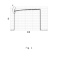
- FIG. 3 is a diagram showing an example of the characteristics of the drain current Ids when the gate is turned on from the pinch-off state in a transmission AMP that is a GaN AMP.
- the horizontal axis shows time
- the vertical axis shows drain current Ids.
- FIG. 4 is an enlarged view of the X portion of FIG. 3.
- FIG. 4 shows the characteristics of Ids when the Vgs setting is changed in four ways.
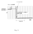
- FIG. 5 shows an example of how the characteristics of the drain current Ids when an impulse is input to a transmitting AMP, which is a GaN AMP with poor drain lag, decreases from the steady setting Ids state value before the impulse is applied. It is a diagram. Further, FIG. 6 is a diagram showing an example of the characteristics of the drain current Ids when an impulse is input to a transmission AMP that is a GaN AMP with a good drain lag. Furthermore, in FIGS. 5 and 6, the horizontal axis represents time, and the vertical axis represents drain current Ids.
- the length of one symbol when Sub Carrier Space is 15kHz is approximately 64 ⁇ sec. Furthermore, in 5G, the length of one symbol when Sub Carrier Space is 30kHz is approximately 36 ⁇ sec, which is approximately half of the length of one symbol of LTE described above.
- the drain current Ids can be returned to the desired Ids within 1 symbol length after inputting the impulse, regardless of whether it is LTE or 5G.
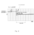
- FIG. 7 is a diagram showing an example of the characteristics of the drain current Ids when a transmission AMP with a good Gate/Drain Lag is a GaN AMP and a transmission AMP with a poor Gate/Drain Lag is turned on.
- the horizontal axis shows time
- the vertical axis shows drain current Ids.
- FIG. 8 is an enlarged view of the X portion of FIG. 7. Note that in FIGS. 7 and 8, no RF modulation signal is input to the transmitting AMP.
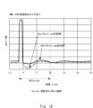
- FIG. 9 is a diagram showing an example of EVM (Error Vector Magnitude) characteristics when the transmitting AMP is turned on in an AAS equipped with a transmitting AMP that is a GaN AMP with poor Gate/Drain Lag.
- FIG. 10 is a diagram showing an example of EVM characteristics when the transmission AMP is turned on in an AAS equipped with a transmission AMP that is a GaN AMP with good Gate/Drain Lag.
- the horizontal axis represents symbols
- the vertical axis represents EVM. Note that in FIGS. 9 and 10, the transmission AMP is turned on and off twice.
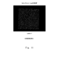
- FIG. 11 is a diagram showing an example of the constellation of Symbol 1 at the beginning of the DL signal immediately after the transmission AMP is turned on in an AAS equipped with a transmission AMP that is a GaN AMP with poor Gate/Drain Lag.
- FIG. 12 is a diagram showing an example of the constellation of the first Symbol 1 of the DL signal immediately after the transmission AMP is turned on in an AAS equipped with a transmission AMP that is a GaN AMP with good Gate/Drain Lag.
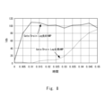
- FIG. 13 shows the relationship between SNR (Signal-to-Noise Ratio) and Throughput for each of multiple MCS (Modulation and channel Coding Schemes) in an AAS equipped with a transmission AMP that is a GaN AMP with poor Gate/Drain Lag.
- FIG. 3 is a diagram showing an example of a relationship.
- FIG. 14 is a diagram showing an example of the relationship between SNR and Throughput for each of a plurality of MCSs in an AAS equipped with a transmission AMP that is a GaN AMP with good Gate/Drain Lag.
- the horizontal axis shows SNR
- the vertical axis shows Throughput.
- an object of the present disclosure is to provide a wireless communication device and a wireless communication method that can maintain the communication quality of the leading portion of a transmission signal.
- a wireless communication device includes: a signal processing section; a transmitter provided after the signal processing section; a transmission amplifier provided after the transmitter,
- the signal processing section includes: Detects the presence or absence of a transmitted signal, When the transmitted signal is detected, a stabilizing signal for stabilizing the characteristics of the transmitting amplifier is inserted into a time domain before the time domain of the transmitted signal, so that the transmitted signal can be detected by the transmitter and the transmitter.
- the stabilized signal is passed through the transmitter and the transmit amplifier before passing through the transmit amplifier.
- a wireless communication method includes: A wireless communication method performed by a wireless communication device including a transmitter and a transmission amplifier provided at a stage subsequent to the transmitter, the method comprising: detecting the presence or absence of a transmission signal at a stage before the transmission amplifier; When the transmission signal is detected, a stabilizing signal for stabilizing the characteristics of the transmission amplifier is inserted into a time domain before the time domain of the transmission signal, so that the transmission signal is transmitted to the transmitter and the transmitter. passing the stabilized signal through the transmitter and the transmit amplifier before passing through the transmit amplifier.
- FIG. 3 is a diagram showing an example of the structure of a GaN/AlGaN HEMT.
- FIG. 3 is a diagram showing an example of a band structure of GaN/AlGaN HEMT.
- FIG. 7 is a diagram showing an example of the characteristics of the drain current Ids when the gate is turned on from a pinch-off state in a transmission AMP that is a GaN AMP. 4 is an enlarged view of the X portion of FIG. 3.
- FIG. FIG. 7 is a diagram showing an example of the characteristics of drain current Ids when an impulse is input to a transmission AMP that is a GaN AMP with poor drain lag.
- FIG. 1 is a diagram showing an example of the structure of a GaN/AlGaN HEMT.
- FIG. 3 is a diagram showing an example of a band structure of GaN/AlGaN HEMT.
- FIG. 7 is a diagram showing an example of the characteristics of the drain current Ids when
- FIG. 7 is a diagram showing an example of the characteristics of drain current Ids when an impulse is input to a transmission AMP that is a GaN AMP with good drain lag.
- FIG. 7 is a diagram showing an example of the characteristics of the drain current Ids when a transmission AMP that is a GaN AMP with good Gate/Drain Lag and a transmission AMP that is a GaN AMP with poor Gate/Drain Lag are respectively turned on.
- 8 is an enlarged view of the X portion of FIG. 7.
- FIG. FIG. 7 is a diagram showing an example of EVM characteristics when the transmission AMP is turned on in an AAS equipped with a transmission AMP that is a GaN AMP with poor Gate/Drain Lag.
- FIG. 7 is a diagram showing an example of EVM characteristics when the transmitting AMP is turned on in an AAS equipped with a transmitting AMP that is a GaN AMP with good Gate/Drain Lag.
- an AAS equipped with a transmission AMP that is a GaN AMP with poor Gate/Drain Lag it is a diagram showing an example of the constellation of the first symbol of a DL signal immediately after the transmission AMP is turned on.
- FIG. 3 is a diagram showing an example of a constellation of the first symbol of a DL signal immediately after the transmission AMP is turned on in an AAS equipped with a transmission AMP that is a GaN AMP with good Gate/Drain Lag.
- FIG. 3 is a diagram showing an example of a constellation of the first symbol of a DL signal immediately after the transmission AMP is turned on in an AAS equipped with a transmission AMP that is a GaN AMP with good Gate/Drain Lag.
- FIG. 7 is a diagram illustrating an example of the relationship between SNR and Throughput for each of a plurality of MCSs in an AAS equipped with a transmission AMP that is a GaN AMP with poor Gate/Drain Lag.
- FIG. 7 is a diagram showing an example of the relationship between SNR and Throughput for each of a plurality of MCSs in an AAS equipped with a transmission AMP that is a GaN AMP with good Gate/Drain Lag.
- Characteristics of the drain current Ids in a state where no RF modulation signal is input when the transmission AMP with a GaN AMP with a good Gate/Drain Lag and the transmission AMP with a GaN AMP with a poor Gate/Drain Lag are turned on.
- FIG. 7 is a diagram showing an example of the characteristics of the deviation of drain current Ids when RF modulation signals having different input levels are input after turning on a transmission AMP that is a GaN AMP with poor Gate/Drain Lag.
- FIG. 7 is a diagram showing an example of the arrangement of AMP stabilization signals in the time direction, frequency direction, and power direction.
- FIG. 3 is a diagram showing an example of arrangement of AMP stabilization signals in the frequency direction and power direction.
- FIG. 7 is a diagram showing an example of the arrangement of AMP stabilization signals in the time direction and frequency direction.
- FIG. 3 is a diagram showing an example of a data structure of an AMP stabilization signal.
- FIG. 3 is a diagram showing an example of time arrangement of AMP stabilization signals.
- 7 is a timing chart showing an example of a change in processing start timing due to an interrupt of an AMP stabilization signal in AAS.
- FIG. 2 is a diagram illustrating a configuration example of an AAS according to an embodiment.
- FIG. 7 is a diagram showing an example in which an AMP stabilization signal is inserted into the time domain before the time domain of the DL signal in the AAS according to the embodiment.
- FIG. 3 is a flowchart illustrating a schematic operation example of AAS according to an embodiment.
- FIG. 7 is a diagram showing an example of the amplitude waveform of a DL signal in an AAS equipped with a transmission AMP that is a GaN AMP with poor Gate/Drain Lag and no AMP stabilization signal provided.
- An example of the amplitude waveform of an AMP stabilization signal and a DL signal is shown in an AAS according to an embodiment that is equipped with a transmission AMP that is a GaN AMP with poor Gate/Drain Lag and provides an AMP stabilization signal to the transmission AMP. It is a diagram.
- FIG. 7 is a diagram showing an example of the amplitude waveform of a DL signal in an AAS equipped with a transmission AMP that is a GaN AMP with poor Gate/Drain Lag and provides an AMP stabilization signal to the transmission AMP.
- FIG. 7 is a diagram showing an example of EVM characteristics when the transmitting AMP is turned on in an AAS equipped with a transmitting AMP that is a GaN AMP with poor Gate/Drain Lag and no AMP stabilization signal provided.
- An example of EVM characteristics when the transmission AMP is turned on in an AAS according to an embodiment that is equipped with a transmission AMP that is a GaN AMP with poor Gate/Drain Lag and provides an AMP stabilization signal to the transmission AMP is shown. It is a diagram.
- FIG. 2 is a diagram illustrating an example hardware configuration of a computer that implements some functions of a wireless communication device according to the present disclosure.
- the wireless communication device equipped with the transmission AMP is an AAS that transmits a DL signal as a transmission signal to each UE.
- the inventor of the present disclosure found that even in a transmitting AMP with poor Gate/Drain Lag, inputting an RF modulation signal after inputting an impulse can shorten the time it takes for the characteristics of the transmitting AMP to stabilize. .
- FIG. 15 shows the drain current in a state where no RF modulation signal is input when the transmission AMP with a GaN AMP with a good Gate/Drain Lag and the transmission AMP with a GaN AMP with a poor Gate/Drain Lag are turned on.
- FIG. 3 is a diagram showing an example of characteristics of Ids.
- the horizontal axis shows time
- the vertical axis shows drain current Ids.
- Figure 16 shows the gain when an RF modulation signal is input together with an impulse for a transmitting AMP that is a GaN AMP with good Gate/Drain Lag and a transmitting AMP that is a GaN AMP with poor Gate/Drain Lag.
- FIG. 2 is a diagram showing an example of the characteristics of In FIG. 16, the horizontal axis shows time and the vertical axis shows Gain.
- the drain current Ids rises slowly immediately after the transmission AMP is turned on when no RF modulation signal is input. Therefore, although not shown in FIG. 15, a long time of approximately 80 ⁇ sec is required until the drain current Ids is restored to the desired Ids.
- the length of one symbol when Sub Carrier Space is 30kHz is approximately 36 ⁇ sec. Therefore, the approximately 80 ⁇ sec required for the drain current Ids to recover corresponds to approximately 2 Symbol lengths of the 5G described above.
- the inventor of the present disclosure has found that even in a transmitting AMP with poor Gate/Drain Lag, the characteristics of the transmitting AMP are stabilized when the input level of the RF modulation signal input to the transmitting AMP is higher after the transmitting AMP is turned on. We have found that it is possible to shorten the time it takes.
- FIG. 17 is a diagram showing an example of the characteristics of the deviation of drain current Ids when RF modulation signals with different input levels are input after turning on a transmitting AMP that is a GaN AMP with poor Gate/Drain Lag. .
- the horizontal axis shows time
- the vertical axis shows the deviation of drain current Ids.
- Idq inle current when no signal is set
- Ids 90mA
- Ids equals 90 mA before inputting the transmission signal.
- the drain current Ids is fixed at 90 mA, and the input level of the RF modulation signal is varied within the range of 33.7 dBm to 45.7 dBm.
- each operating CC Component Carrier setting
- the AMP stabilization signal is inserted into the time domain immediately before the time domain of the DL signal.
- the AM-AM/AM-PM characteristics of the transmitting AMP in the first symbol section of the DL signal are already stable, so the first symbol of the DL signal and subsequent Symbols are stably compensated for distortion by the DPD in the TX, which is the transmitter. This also contributes to ensuring the signal quality of the DL signal from the first Symbol.
- TX is provided within TRX, which is a transmitter/receiver.
- FIG. 18 is a diagram showing an example of the arrangement of the AMP stabilization signal in the time direction, frequency direction, and power direction.
- FIG. 19 is a diagram showing an example of arrangement of the AMP stabilization signal in the frequency direction and the power direction.
- FIG. 20 is a diagram showing an example of the arrangement of the AMP stabilization signal in the time direction and frequency direction. Note that in FIGS. 18 to 20, it is assumed that the DL signal is a signal for each slot or a signal for each symbol.
- the AMP stabilization signal is, for example, a signal in OFDM (Orthogonal Frequency Division Multiplexing) Format.
- the AMP stabilized signal is a signal having an amplitude probability density of a Reighley distribution with a PAPR (Peak to Average Power Ratio) of 14 dB.
- the AMP stabilized signal passes through the CFR (Crest Factor Reduction) placed before the DPD in the TX, and then the PAPR of the AMP stabilized signal is soft clipped to the CFR threshold (about 7 to 8 dB). be done.
- CFR Rest Factor Reduction
- the AMP stabilization signal is placed in the time area before the first Symbol of the DL Slot or any Symbol in the DL Slot.
- a transient period called a Tx On Transient period is set as a period for switching TX from Off to On. Therefore, in the situation under TDD system, the AMP stabilization signal will be placed in the time domain within the Tx On Transient period before the DL signal.
- the Tx On Transient period is specified as 10 ⁇ sec. .
- the time width of the signal obtained by adding Ramp Up/Down to the AMP stabilization signal is set to within 10 ⁇ s.
- Ramp Up/Down is a signal inserted to prevent impulse spectrum spreading.
- the time width of the DL signal is approximately 36 ⁇ sec to several DL slots.
- the time width of the DL signal is 140 ⁇ sec when operating in SSB (SS (Synchronization Signal)/PBCH (Physical Broadcast CHannel) Block).
- SSB is a synchronization signal/broadcast channel block composed of SS and PBCH.
- SSB is sent periodically from base stations mainly for terminals to detect cell ID and reception timing when starting communication, but in 5G NR it is also used to measure the reception quality of each cell.
- the frequency bandwidth of the AMP stabilization signal is set to a wide band equivalent to the frequency bandwidth of each Component Carrier used for transmitting the DL signal.
- the frequency bandwidth of each Component Carrier is approximately 20MHz to 100MHz.
- the frequency bandwidth of the DL signal is approximately 7.2 MHz when operating in SSB, and the frequency bandwidth of each Component Carrier under actual DL signals such as PDSCH (Physical Downlink Shared CHannel).
- increasing the input level of the RF modulation signal further promotes early recovery of the characteristics of the transmitting AMP. Therefore, the power level of the AMP stabilization signal is set to a high level at which the output of the transmitting AMP reaches the maximum rated RMS (Root Mean Square) level and the same power level as the DL signal.
- the AMP stabilization signal is Pass the stabilized signal through the transmitting AMP.
- the AM-AM/AM-PM characteristics of the transmitting AMP in the first symbol section of the DL signal are already stable, so the first symbol of the DL signal and subsequent Symbols are stably compensated for distortion by DPD in TX. This also contributes to ensuring the signal quality of the DL signal from the first Symbol.
- the AMP stabilization signal is placed in the time domain within the Tx On Transient period before the DL signal, but in 3GPP NR, the Tx On Transient period is defined as 10 ⁇ sec. Therefore, within 10 ⁇ s of the Tx On Transient period, the nonlinear distortion characteristics such as AM-PM of the transmitting AMP are stabilized, and then the DL signal is subjected to distortion compensation by DPD.
- FIG. 21 is a diagram showing an example of the data structure of the AMP stabilization signal.
- the AMP stabilization signal has a structure in which a CP (Cyclic Prefix) is added to the beginning of the data part, Ramp up and Ramp down are added before and after it, and the last part is null. .
- Ramp up is 188 samples
- CP is 8 samples
- data part is 2048 samples
- Ramp down is 188 samples
- null 128 samples.
- the total of Ramp up, CP, data part, and Ramp down is 2432 samples, and the total including nulls is 2560 samples.
- Transmission speed 245.76MSPS
- Frequency bandwidth Frequency bandwidth of Component Carrier
- Power level Power level at which the output of the transmitting AMP reaches the maximum rated RMS level
- Modulation method QPSK (Quadrature Phase-Shift Keying) ⁇ 256QAM PAPR:14dB. 7-8dB after passing through CFR
- FIG. 22 is a diagram showing an example of the time arrangement of the AMP stabilization signal.
- the AMP stabilization signal is placed, for example, in a time domain within the Tx On Transient period, which is a period for switching TX from Off to On.
- the Tx On Transient period is defined as 10 ⁇ sec in 3GPP NR.
- FIG. 23 is a timing chart showing an example of a change in processing start timing due to an interrupt of an AMP stabilization signal in AAS.
- the AAS interrupts the AMP stabilization signal into the time domain before the time domain of the DL signal. Therefore, assuming that the AMP stabilization signal has a length corresponding to 10 ⁇ sec, the AAS advances the timing of applying the control voltage TX_Enable On for enabling the TX in the TRX to the TX by 10 ⁇ sec. AAS also advances the timing of applying the control voltage AMP On for turning on the transmitting AMP to the transmitting AMP by 10 ⁇ sec.
- Embodiments of a wireless communication device according to the present disclosure will be described below. The following description will be made assuming that the wireless communication device according to the present embodiment is an AAS that transmits a DL signal as a transmission signal to each UE.
- FIG. 24 is a diagram showing a configuration example of the AAS 10 according to the present embodiment. Note that FIG. 24 shows only the main components of the AAS 10 according to this embodiment, and other components (for example, antennas, etc.) are not shown.
- the AAS 10 includes a signal processing unit 11, a TX 12 that is a transmitter, and a transmission AMP 13 that is a GaN AMP. Further, the signal processing section 11 includes a detection section 111, an IFFT (Inverse Fast Fourier Transform) section 112, a signal storage memory 113, and an adder 114.
- IFFT Inverse Fast Fourier Transform
- the IFFT unit 112 converts the DL signal from a frequency domain signal to a time domain signal.
- the detection section 111 is provided before the IFFT section 112.
- the detection unit 111 autonomously detects the presence or absence of a DL signal in the frequency domain. For example, the detection unit 111 detects the presence or absence of a DL signal by performing threshold determination in the frequency domain.
- the signal storage memory 113 stores an AMP stabilization signal for stabilizing the characteristics of the transmitting AMP 13. Specifically, when the AMP stabilization signal is input to the transmitting AMP 13, it quickly converges the current collapse and Gate/Drain Lag of the transmitting AMP 13, and quickly stabilizes the gain, output, and nonlinear distortion characteristics of the transmitting AMP 13. It is a signal that causes
- the adder 114 stores the DL signal in the signal storage memory 113 in a time domain before the time domain of the DL signal after the DL signal is output from the IFFT unit 112. Add the AMP stabilization signal. In this way, the AMP stabilization signal is inserted into the time domain before the time domain of the DL signal. At this time, the adder 114 calculates back the time at which the DL signal exists, taking into account the processing time of the TX 12 from the radiation time of the DL signal from the antenna, and inserts the AMP stabilization signal at the beginning of that time. .
- the AMP stabilization signal is inserted into the time domain before the time domain of the DL signal.
- the AMP stabilization signal can be passed through the TX 12 and the transmission AMP 13 before the DL signal passes through the TX 12 and the transmission AMP 13.
- the time domain before the time domain of the DL signal is, for example, the Tx On Transient period, which is a period for switching the TX 12 from Off to On. Therefore, the time width of the AMP stabilization signal is set within the time width of Tx On Transient period.
- Tx On Transient period is specified as 10 ⁇ sec in 3GPP NR.
- the frequency bandwidth of the AMP stabilization signal is set to the frequency bandwidth of the Component Carrier used for transmitting the DL signal.
- the power level of the AMP stabilization signal is set to a power level at which the output of the transmitting AMP 13 reaches the maximum rated RMS level, and is set to the same power level as the DL signal.
- the TX 12 is provided after the signal processing unit 11, and converts the DL signal or AMP stabilization signal output from the signal processing unit 11 from an IQ (In-Phase/Quadrature-Phase) signal to an RF signal. , output to the transmitting AMP 13.
- the TX 12 is provided in a TRX (not shown) that is a transmitter/receiver. Further, as described above, the TX 12 includes a DPP, a CFR provided before the DPD, etc., but illustration of these is omitted.
- the transmission AMP 13 is provided after the TX 12, and amplifies and outputs the DL signal or AMP stabilization signal output from the TX 12.
- the DL signal or AMP stabilization signal output from the transmission AMP 13 is transmitted to each UE via an antenna (not shown).
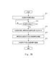
- FIG. 26 is a flowchart showing a schematic example of the operation of the AAS 10 according to the present embodiment.
- the detection unit 111 detects the presence or absence of a DL signal (step S11). If the detection unit 111 detects the DL signal (Yes in step S12), the adder 114 inserts the AMP stabilization signal into the time domain before the time domain of the DL signal (step S13). Therefore, first, the AMP stabilization signal passes through the TX 12 and the transmitting AMP 13 (step S14), thereby stabilizing the gain, output, and nonlinear distortion characteristics of the transmitting AMP 13. After that, the DL signal passes through the TX 12 and the transmission AMP 13 (step S15).
- the signal processing unit 11 when the signal processing unit 11 detects the DL signal, the signal processing unit 11 interrupts the AMP stabilization signal in the time domain before the time domain of the DL signal, so that the DL signal is connected to the TX 12 and Before passing through the transmission AMP 13, the AMP stabilization signal is passed through the TX 12 and the transmission AMP 13.
- the AM-AM/AM-PM characteristics of the transmitting AMP 13 in the first symbol section of the DL signal are already stable, so the first symbol of the DL signal and subsequent Symbols are stably compensated for distortion by the DPD within the TX 12. This also contributes to ensuring the signal quality of the DL signal from the first Symbol.
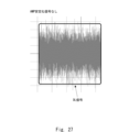
- FIG. 27 is a diagram showing an example of the amplitude waveform of a DL signal in an AAS equipped with a transmission AMP that is a GaN AMP with poor Gate/Drain Lag and no AMP stabilization signal provided.
- FIG. 28 shows the AMP stabilization signal and DL signal in the AAS 10 according to the present embodiment, which is equipped with a transmission AMP 13 that is a GaN AMP with poor Gate/Drain Lag and provides an AMP stabilization signal to the transmission AMP 13.
- FIG. 3 is a diagram showing an example of an amplitude waveform of FIG. In FIGS. 27 and 28, the horizontal axis shows time, and the vertical axis shows amplitude. The difference in amplitude waveforms in FIGS. 27 and 28 appears as a difference in EVM characteristics in FIGS. 29 and 30, which will be described later.
- FIG. 29 is a diagram showing an example of EVM characteristics when the transmitting AMP is turned on in an AAS equipped with a transmitting AMP that is a GaN AMP with poor Gate/Drain Lag and no AMP stabilization signal provided.
- FIG. 30 shows when the transmitting AMP 13 is turned on in the AAS 10 according to the present embodiment, which is equipped with the transmitting AMP 13 which is a GaN AMP with poor Gate/Drain Lag and gives an AMP stabilization signal to the transmitting AMP 13.
- FIG. 3 is a diagram showing an example of EVM characteristics.
- the horizontal axis represents Symbol
- the vertical axis represents EVM. Note that in FIGS. 29 and 30, the transmission AMP is turned on/off only once.
- FIG. 31 shows the DL signal immediately after turning on the transmitting AMP 13 in the AAS 10 according to the present embodiment, which is equipped with the transmitting AMP 13 which is a GaN AMP with poor Gate/Drain Lag and gives an AMP stabilization signal to the transmitting AMP 13.
- FIG. 3 is a diagram showing an example of a constellation of the first Symbol 1 of FIG.
- an example of the constellation of the first Symbol 1 of the DL signal immediately after turning on the transmitting AMP is shown in Figure 11. It is the same as the one above.
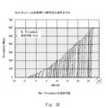
- FIG. 32 shows the SNR and FIG. 3 is a diagram showing an example of the relationship with throughput.
- the horizontal axis shows SNR and the vertical axis shows Throughput.
- an example of the relationship between SNR and Throughput for each of multiple MCSs in an AAS equipped with a transmitting AMP with poor Gate/Drain Lag and no AMP stabilization signal is shown in Figure 13. The same is true.
- the wireless communication device according to the present disclosure is used for AAS, but the present disclosure is not limited to this.
- the wireless communication device according to the present disclosure can be used in any wireless communication device (for example, a wide area base station, a macro base station, etc.) that has a transmission function to transmit a transmission signal.
- FIG. 33 is a diagram illustrating an example of the hardware configuration of the computer 20 that implements some of the functions of the wireless communication device according to the present disclosure. As shown in FIG. 33, the computer 20 includes a processor 21 and a memory 22.
- the processor 21 may be, for example, a microprocessor, a CPU, or an MPU (Micro Processing Unit). Processor 21 may include multiple processors.
- the memory 22 is configured by a combination of volatile memory and nonvolatile memory.
- Memory 22 may include storage located remotely from processor 21.
- the processor 21 may access the memory 22 via an I (Input)/O (Output) interface (not shown).
- a program is stored in the memory 22.
- This program includes a group of instructions (or software code) for causing the computer 20 to perform some of the functions of the AAS 10 according to the embodiment described above when loaded into the computer 20.
- the components of the AAS 10 described above may be realized by the processor 21 reading and executing a program stored in the memory 22. Further, the component having the storage function in the AAS 10 described above may be realized by the memory 22.
- the above-mentioned program may be stored in a non-transitory computer-readable medium or a tangible storage medium.
- computer readable or tangible storage media may include random-access memory (RAM), read-only memory (ROM), flash memory, solid-state drive (SSD) or other memory technology, CD - Including ROM, digital versatile disc (DVD), Blu-ray disc or other optical disc storage, magnetic cassette, magnetic tape, magnetic disc storage or other magnetic storage device.
- the program may be transmitted on a transitory computer-readable medium or a communication medium.
- transitory computer-readable or communication media includes electrical, optical, acoustic, or other forms of propagating signals.
Abstract
本開示に係るAAS(10)は、信号処理部(11)と、信号処理部(11)の後段に設けられた送信機(12)と、送信機(12)の後段に設けられた送信アンプ(13)と、を備える。信号処理部(11)は、送信信号の有無を検出し、送信信号を検出した場合、送信アンプ(13)の特性を安定化させるための安定化信号を、送信信号の時間域の前の時間域に割り込ませることで、送信信号が送信機(12)及び送信アンプ(13)を通過する前に、安定化信号を送信機(12)及び送信アンプ(13)を通過させる。
Description
本開示は、無線通信装置及び無線通信方法に関する。
GaNは、GaAsと比較すると、バンドギャップエネルギーが大きく、高耐圧、微細化が可能とされている点と、電子移動度が高い点と、で利点がある。そのため、GaN FET(Field Effect Transistor)を用いる送信AMP等のRF(Radio Frequency)デバイスは、GaAs FETを用いるRFデバイスを超える高出力なRFデバイスとして、Wide Area向け基地局、マクロ基地局、AAS(Antenna Active System)等の無線通信装置への採用が続いている。また、GaN/AlGaN FETの2次元電子ガス構造は、Si FETと比較して、移動度が高い等の物理特性がある。そのため、GaN/AlGaN FETを用いるRFデバイスは、特に、RFの高周波帯での高出力なRFデバイスとして採用及び実用化されている。GaN/AlGaN FETの例としては、GaN/AlGaN HEMT(High Electron Mobility Transistor)が挙げられる。
図1は、GaN/AlGaN HEMTの構造例を示す図である。また、図2は、GaN/AlGaN HEMTのバンド構造例を示す図である。図1及び図2に示されるように、GaN/AlGaN HEMTは、サファイア基板上にGaN/AlGaNを成長させることで実現される。GaN/AlGaN HEMTでは、異種化合物材料の境界に生じた2次元電子ガスと呼ばれる電子層をキャリアとして用い、電子供給層(AlGaN層)と電子走行層(GaN層)とが異なっている。そのため、GaN/AlGaN HEMTは、高電子移動度を実現でき、高速及び高周波での利用が可能でかつ大電力出力が高効率で可能になるという利点がある。
AlGaN/GaN HEMTを大振幅及び大電力で稼働させる場合、様々な寄生現象についての工面が必要となる。現在、AlGaN/GaN HEMTでは、GaN半絶縁基板、表面準位、及び基板界面に存在する深い不純物準位に起因した、様々な寄生現象が知られている。これらの寄生現象は、AlGaN/GaN HEMTを用いるRFデバイスの出力電力、歪特性、安定性、信頼性の面で問題となっている。半導体の表面準位については、半導体の結晶内部ではエネルギー準位が決まっている。しかし、半導体の表面では、連続性が途切れている場合、結晶内部とは異なるエネルギー準位(=表面準位)が存在することになる。この表面準位は、結晶表面での再配列や、酸素原子、水素原子等の外部の原子を吸着する等で形成されるため、理論的な解析は非常に複雑化してしまう。そのため、この表面準位に起因する寄生現象を克服する難易度は高い。
また、これら寄生現象の中で、電流コラプスと呼ばれる現象は、ドレイン電圧を印加していくと、ドレイン電流が減ってしまう現象である。電流コラプスに関しては、例えば、特許文献1に記載されている。送信AMPの動作級をA級→AB級→C級→・・・と変更し、送信AMPの高効率化及び大電力化を目指す場合は、さらに、送信信号の振幅に応じたドレイン電流の増減を伴う。ドレイン電流の増減は、時間的に過去の振幅増幅動作の履歴によって、現在の利得及び出力が低下及び変動する等の不安定要因(メモリー効果)となっており、DPD(Digital Pre-Distortion)による歪改善の難易度が上がることとなる。
また、送信AMPでは、Drain Lag及びGate Lagという過渡現象も問題となる。C級以上の送信AMPでは、送信信号のある一定以上の振幅に応じて、ドレイン電流が流れる事でC級増幅が始まり、送信AMPの出力を整合する整合回路(基本波としての増幅信号を含む高調波群増幅後信号から基本波のみを抽出出力するタンク回路)により基本増幅信号が出力される。Drain Lagとは、ドレイン電圧を急激にOff→Onとして送信AMPの増幅動作を可能とした際、ドレイン電流が定常電圧状態に至るまで、過渡的かつ緩慢に変化してしまう現象である。また、送信AMPを搭載した無線通信装置は、TDD(Time Division Duplex)での動作時は、UL(Up Link)/DL(Down Link)の切り替えに伴い、送信AMPのOff/Onを行う。送信AMPのOff/Onの立ち上げはVgsをPinch-off状態(Ids=0A状態にする深めVgs設定)から、所望のAMP性能を得る為のIds設定値となる様に、浅めVgs電圧へ切り替え制御を行う事により、所望のIdsが設定され、送信AMP On動作に至るが、その時にゲート電圧の急激な変化が生じる。Gate Lagは、このゲート電圧の急激な変化(Gate Pinch-OffでIds Off、送信AMPが完全Off状態 → 送信AMP OnのIds設定を行うゲート電圧へ急変)に対して、ドレイン電流が定常電圧状態に至るまで、過渡的かつ緩慢に変化してしまう現象である。これらGate Lag及びDrain Lag(以下、適宜「Gate/Drain Lag」と称す)も、AlGaN/GaN HEMTを用いる送信AMPが、TDD動作を行うべく、高速なOff/On動作及びバースト動作を行う場合、正常状態に至るまでの過渡応答遅れの不全を招く。正常状態とは、Gain、出力、AM(Amplitude Modulation)-AM/AM-PM(Phase Modulation)等の非線形歪特性が定常状態になることを意味する。ここで、LTE(Long Term Evolution)や5G(Fifth Generation Partnership Project)の基地局は、TDDシステム下にある状況では、送信AMPを時間的にOn/Offするバースト動作や、送信Symbolに応じて送信AMPをこまめにOn/Offする動作によって、低消費電力の適応制御を行う。その際、上述した過渡応答遅れのために、送信AMPのOn制御の顕著な前倒しが必要となることから、送信信号の安定化までに多くの時間を要してしまっていた。
送信AMPにおいて、上述したGate/Drain Lagといった過渡現象が発生する場合、AMP基板(AMP内部のベア・チップ・ダイのSubstrate基板部)の深い準位や表面準位の帯電状態により、充放電がある一定の時定数を持ってしまう。このことから、送信AMPへの送信信号の入力前に、送信AMPのOff/Onのために、ドレイン電流が、目標とする定常ドレイン電流に至るまでの時間が大きく遅延してしまう。その結果、送信信号が送信AMPを通過する時に、送信信号の先頭部分のGain、出力、非線形歪特性が、定常状態に至らなくなる。このことは、上述した低消費電力の適応制御において、送信AMPをOnする度に、送信AMPの安定した特性が確保できないことに繋がる。
これに伴い、LTEや5Gの基地局が、GaN FETを用いる送信AMPを採用した場合、TDDシステム下にある状況では、上述した低消費電力の適応制御等を行うことが困難となるため、TDDシステムのシステム特性に対して多々の不具合を発生させることとなる。
以下、上述した問題について、図面を参照して説明する。以下では、GaN FETを用いるAMPを、適宜、「GaN AMP」と称す。また、以下では、送信AMPが搭載される無線通信装置が、各UE(User Equipment:携帯端末)に対し、送信信号としてDL信号を送信するAASであるものとする。
図3は、GaN AMPである送信AMPにおいて、ゲートをピンチオフ状態からOnした時のドレイン電流Idsの特性の例を示す図である。図3において、横軸は時間を示し、縦軸はドレイン電流Idsを示している。また、図4は、図3のX部分を拡大した拡大図である。図4においては、Vgsの設定を4通りにそれぞれ変化させた時の、Idsの特性を示している。
図3に示されるように、ゲートをピンチオフ状態からOnすることで、ゲート電圧が急激に増大するため、ドレイン電流Idsは、所望Idsに至るまで過渡的かつ緩慢に変化しており、Gate Lagが発生している。また、図4に示されるように、VgsをVgsが深いPinch-Off状態より浅く設定して、ゲートをOnした方が、ゲートをOnした後に、ドレイン電流Idsが所望Idsに至るまでの時間が早まる傾向にある。
図5は、Drain Lagが劣悪なGaN AMPである送信AMPに対し、インパルスを入力した時のドレイン電流Idsの特性が如何にインパルス印加前の定常設定Ids状態値から低下しているかの一例を示す図である。また、図6は、Drain Lagが良好なGaN AMPである送信AMPに対し、インパルスを入力した時のドレイン電流Idsの特性の例を示す図である。また、図5及び図6において、横軸は時間を示し、縦軸はドレイン電流Idsを示している。
図5に示されるように、Drain Lagが劣悪な送信AMPに対し、インパルスを入力した場合、入力直後に、ドレイン電流Idsが約90%低下する。そのため、ドレイン電流Idsを所望Idsに復帰させるまで長時間が必要となる。
ここで、LTEにおいて、Sub Carrier Spaceが15kHzである時の1Symbol長は、約64μsecである。また、5Gにおいて、Sub Carrier Spaceが30kHzである時の1Symbol長は、上述したLTEの1Symbol長の約1/2に相当する、約36μsecである。
そのため、Drain Lagが劣悪な送信AMPの場合、LTE又は5Gのどちらの場合であっても、インパルスの入力後から1Symbol長以内に、ドレイン電流Idsを所望Idsに復帰させることは困難である。
一方、図6に示されるように、Drain Lagが良好な送信AMPに対し、インパルスを入力した場合、入力直後のドレイン電流Idsの低下は、約40%に留まる。そのため、ドレイン電流Idsを、短時間で所望Idsに復帰させることできる。
そのため、Drain Lagが良好な送信AMPの場合、LTE又は5Gのどちらの場合であっても、インパルスの入力後から1Symbol長以内に、ドレイン電流Idsを所望Idsに復帰させることできる。
図7は、Gate/Drain Lagが良好なGaN AMPである送信AMP及びGate/Drain Lagが劣悪なGaN AMPである送信AMPをそれぞれOnした時のドレイン電流Idsの特性の例を示す図である。図7において、横軸は時間を示し、縦軸はドレイン電流Idsを示している。また、図8は、図7のX部分を拡大した拡大図である。なお、図7及び図8においては、送信AMPに対するRF変調信号の入力は無い状態になっている。
図7及び図8に示されるように、Gate/Drain Lagが良好な送信AMPの場合、送信AMPをOnした直後のドレイン電流Idsの立ち上がり特性は良好である。そのため、ドレイン電流Idsを、短時間で所望Idsに復帰させることできる。これに対して、Gate/Drain Lagが劣悪な送信AMPの場合、送信AMPをOnした直後のドレイン電流Idsは、緩やかに立ち上がることになる。そのため、ドレイン電流Idsを所望Idsに復帰させるまで長時間が必要となる。
図9は、Gate/Drain Lagが劣悪なGaN AMPである送信AMPを搭載したAASにおいて、送信AMPをOnした時のEVM(Error Vector Magnitude)の特性の例を示す図である。また、図10は、Gate/Drain Lagが良好なGaN AMPである送信AMPを搭載したAASにおいて、送信AMPをOnした時のEVMの特性の例を示す図である。図9及び図10において、横軸はSymbolを示し、縦軸はEVMを示している。なお、図9及び図10においては、送信AMPのOn/Offを2回繰り返している。
図9に示されるように、Gate/Drain Lagが劣悪な送信AMPを搭載したAASの場合、送信AMPをOnした直後のDL信号においては、先頭Symbol 1のEVMは、Overshootが発生しており、劣化している。これに対して、図10に示されるように、Gate/Drain Lagが良好な送信AMPを搭載したAASの場合、送信AMPをOnした直後のDL信号においては、先頭Symbol 1から、EVMは、Overshootが抑制されており、劣化していない。
図11は、Gate/Drain Lagが劣悪なGaN AMPである送信AMPを搭載したAASにおいて、送信AMPをOnした直後のDL信号の先頭Symbol 1のコンスタレーションの例を示す図である。また、図12は、Gate/Drain Lagが良好なGaN AMPである送信AMPを搭載したAASにおいて、送信AMPをOnした直後のDL信号の先頭Symbol 1のコンスタレーションの例を示す図である。
図11に示されるように、Gate/Drain Lagが劣悪な送信AMPを搭載したAASの場合、送信AMPをOnした直後のDL信号の先頭Symbol 1のコンスタレーションは、位相回転が発生している。なお、図示していないが、Symbol 1以降のSymbolのコンスタレーションは、正常であることが確認された。これに対して、図12に示されるように、Gate/Drain Lagが良好な送信AMPを搭載したAASの場合、送信AMPをOnした直後のDL信号は、先頭Symbol 1から、コンスタレーションが正常である。
図13は、Gate/Drain Lagが劣悪なGaN AMPである送信AMPを搭載したAASにおいて、複数のMCS(Modulation and channel Coding Scheme)の各々について、SNR(Signal-to-Noise Ratio)とThroughputとの関係の例を示す図である。また、図14は、Gate/Drain Lagが良好なGaN AMPである送信AMPを搭載したAASにおいて、複数のMCSの各々について、SNRとThroughputとの関係の例を示す図である。図13及び図14において、横軸はSNRを示し、縦軸はThroughputを示している。
上述したように、GaN AMPである送信AMPを搭載したAASにおいては、Gate/Drain Lagが発生した場合、送信AMPをOnした直後に、DL信号の先頭SymbolのEVMにOvershootが発生する。そのため、Gate/Drain Lagが発生した場合、TDD DL/UL Configuration毎の DL Slotの先頭Symbolや、 DL Slot中の任意の先頭Symbolにおいて、EVMにOvershootが発生する。
そのため、図13に示されるように、Gate/Drain Lagが劣悪な送信AMPを搭載したAASの場合、特に、MCSの最大方向(高次QAM(Quadrature Amplitude Modulation))側では、SNRに応じたMax Throughputが達成できなくなる。そのため、SNRが約20dB以上のMCSが達成できない事となってしまう。これに対して、図14に示されるように、Gate/Drain Lagが良好な送信AMPを搭載したAASの場合、最大のMCSまで、SNRに応じたMax Throughputが達成できる。
以上の通り、Gate/Drain Lagが劣悪な送信AMPを搭載した無線通信装置においては、送信AMPの特性が安定化するまでの遅延があるために、送信信号の先頭部分の通信品質が悪化し、これに起因して、多々の不具合を発生させてしまうという問題があった。
本開示の目的は、上述した課題を鑑み、送信信号の先頭部分の通信品質を維持することが可能な無線通信装置及び無線通信方法を提供することにある。
一態様による無線通信装置は、
信号処理部と、
前記信号処理部の後段に設けられた送信機と、
前記送信機の後段に設けられた送信アンプと、を備え、
前記信号処理部は、
送信信号の有無を検出し、
前記送信信号を検出した場合、前記送信アンプの特性を安定化させるための安定化信号を、前記送信信号の時間域の前の時間域に割り込ませることで、前記送信信号が前記送信機及び前記送信アンプを通過する前に、前記安定化信号を前記送信機及び前記送信アンプを通過させる。
信号処理部と、
前記信号処理部の後段に設けられた送信機と、
前記送信機の後段に設けられた送信アンプと、を備え、
前記信号処理部は、
送信信号の有無を検出し、
前記送信信号を検出した場合、前記送信アンプの特性を安定化させるための安定化信号を、前記送信信号の時間域の前の時間域に割り込ませることで、前記送信信号が前記送信機及び前記送信アンプを通過する前に、前記安定化信号を前記送信機及び前記送信アンプを通過させる。
一態様による無線通信方法は、
送信機と、前記送信機の後段に設けられた送信アンプと、を備える無線通信装置により実行される無線通信方法であって、
前記送信アンプの前段で送信信号の有無を検出するステップと、
前記送信信号を検出した場合、前記送信アンプの特性を安定化させるための安定化信号を、前記送信信号の時間域の前の時間域に割り込ませることで、前記送信信号が前記送信機及び前記送信アンプを通過する前に、前記安定化信号を前記送信機及び前記送信アンプを通過させるステップと、を含む。
送信機と、前記送信機の後段に設けられた送信アンプと、を備える無線通信装置により実行される無線通信方法であって、
前記送信アンプの前段で送信信号の有無を検出するステップと、
前記送信信号を検出した場合、前記送信アンプの特性を安定化させるための安定化信号を、前記送信信号の時間域の前の時間域に割り込ませることで、前記送信信号が前記送信機及び前記送信アンプを通過する前に、前記安定化信号を前記送信機及び前記送信アンプを通過させるステップと、を含む。
上述の態様によれば、送信信号の先頭部分の通信品質を維持することが可能な無線通信装置及び無線通信方法を提供できるという効果が得られる。
以下、図面を参照して本開示の実施の形態について説明する。なお、以下の記載及び図面は、説明の明確化のため、適宜、省略及び簡略化がなされている。また、以下の各図面において、同一の要素には同一の符号が付されており、必要に応じて重複説明は省略されている。また、以下で示す具体的な数値等は、本開示の理解を容易とするための例示にすぎず、これに限定されるものではない。
<実施の形態の原理>
本実施の形態の詳細を説明する前に、本実施の形態の原理について説明する。以下でも、送信AMPが搭載される無線通信装置が、各UEに対し、送信信号としてDL信号を送信するAASであるものとする。
本実施の形態の詳細を説明する前に、本実施の形態の原理について説明する。以下でも、送信AMPが搭載される無線通信装置が、各UEに対し、送信信号としてDL信号を送信するAASであるものとする。
本開示の発明者は、Gate/Drain Lagが劣悪な送信AMPでも、インパルスを入力した後、RF変調信号を入力した方が、送信AMPの特性が安定化するまでの時間を短縮できることを見出した。
図15は、Gate/Drain Lagが良好なGaN AMPである送信AMP及びGate/Drain Lagが劣悪なGaN AMPである送信AMPをそれぞれOnした時の、RF変調信号の入力が無い状態でのドレイン電流Idsの特性の例を示す図である。図15において、横軸は時間を示し、縦軸はドレイン電流Idsを示している。また、図16は、Gate/Drain Lagが良好なGaN AMPである送信AMP及びGate/Drain Lagが劣悪なGaN AMPである送信AMPのそれぞれに対し、インパルスと共に、RF変調信号を入力した時のGainの特性の例を示す図である。図16において、横軸は時間を示し、縦軸はGainを示している。
図15に示されるように、Gate/Drain Lagが劣悪な送信AMPの場合、RF変調信号の入力が無い状態では、送信AMPをOnした直後のドレイン電流Idsは、緩やかに立ち上がる。そのため、図15には図示できていないが、ドレイン電流Idsを所望Idsに復帰させるまで、約80μsecの長時間が必要となる。上述したように、5Gにおいて、Sub Carrier Spaceが30kHzである時の1Symbol長は、約36μsecである。そのため、ドレイン電流Idsが復帰するまでの約80μsecは、上述した5Gの約2 Symbol長分の時間に相当する。
これに対して、図16に示されるように、Gate/Drain Lagが劣悪な送信AMPでも、インパルスと共に、RF変調信号を入力した場合には、インパルス入力前のGainに復帰するまでの時間は、約10μsecであり、Gainが復帰するまでの時間を短縮できる。Gainが復帰するまでの約10μsecは、上述した5Gの約0.3 Symbol長分の時間に相当する。
また、本開示の発明者は、Gate/Drain Lagが劣悪な送信AMPでも、送信AMPをOnした後に送信AMPに入力するRF変調信号の入力レベルが高い方が、送信AMPの特性が安定化するまでの時間を短縮できることを見出した。
図17は、Gate/Drain Lagが劣悪なGaN AMPである送信AMPをOnした後、入力レベルが互いに異なるRF変調信号をそれぞれ入力した場合のドレイン電流Idsの偏差の特性の例を示す図である。図17において、横軸は時間を示し、縦軸はドレイン電流Idsの偏差を示している。ここで、縦軸のIdsの偏差は、Idq(無信号時設定時のアイドルカレント)をIds=90mAとし、その後、送信信号を送信AMPに入力した後の各時間での信号増幅時のIdsを、送信信号を送信AMPに印加する前のIds=Idqとの差分として表したものである。従って、同図縦軸上での“0(A)”は、送信信号入力前のIds=90mAに一致している事を意味する。なお、図17においては、ドレイン電流Idsを90mAで固定し、RF変調信号の入力レベルを33.7dBm~45.7dBmの範囲内で変化させている。
図17に示されるように、Gate/Drain Lagが劣悪な送信AMPでも、送信AMPをOnした後に送信AMPに入力するRF変調信号の入力レベルが高い方が、元のドレイン電流Ids(=90mA)に復帰するまでの時間を短縮できる。図17の例では、RF変調信号の入力レベルを、最も高い45.7dBmにした時が、元のドレイン電流Idsに復帰するまでの時間が最も短縮された。
そこで、本実施の形態においては、上述した知見に基づいて、DL信号の時間域の前の時間域に、高レベルでかつインパルスの周波数特性同様、可能な限り広帯域(各運用CC:Component Carrier設定まで周波数拡張可能)なAMP安定化信号を割り込ませることで、DL信号が送信AMPを通過する前に、AMP安定化信号を送信AMPを通過させる。なお、AMP安定化信号は、DL信号の時間域の直前の時間域に割り込ませることが好適である。
このようにして、DL信号の先頭Symbolが送信AMPに入力される前に、AMP安定化信号を送信AMPに入力することによって、送信AMPの電流コラプス及びGate/Drain Lagを早期に解消させる。これにより、送信AMPの電流コラプス及びGate/Drain Lagに起因する特性変異を早期に収束させ、送信AMPのGain、出力、AM-AM/AM-PM等の非線形歪特性を安定化させることができる。これにより、DL信号の先頭SymbolのEVMのOvershootに起因する、多々の不具合の発生が回避されるため、DL信号の先頭SymbolやDL Slot中の任意の先頭Symbolから信号品質が保証される。また、DL信号の先頭Symbolが送信AMPに入力された時点では、DL信号の先頭Symbol区間での送信AMPのAM-AM/AM-PM特性が予め安定となっているため、DL信号の先頭Symbol及び以降のSymbolは、送信機であるTX内のDPDで安定的に歪補償される。このことも、DL信号が、先頭Symbolから、信号品質が保証されることに寄与する。なお、TXは、送受信機であるTRX内に設けられる。
図18は、AMP安定化信号の時間方向、周波数方向、及び電力方向の配置例を示す図である。また、図19は、AMP安定化信号の周波数方向及び電力方向の配置例を示す図である。また、図20は、AMP安定化信号の時間方向及び周波数方向の配置例を示す図である。なお、図18~図20において、DL信号は、Slot単位の信号又はSymbol単位の信号であるとする。
図18~図20に示されるように、AMP安定化信号は、例えば、OFDM(Orthogonal Frequency Division Multiplexing) Formatの信号である。また、AMP安定化信号は、PAPR(Peak to Average Power Ratio)が14dBのReighley分布の振幅確率密度を有する信号である。また、AMP安定化信号は、TX内のDPDの前段に配置されたCFR(Crest Factor Reduction)を通過し、その後、AMP安定化信号のPAPRは、CFRの閾値(約7~8dB)にSoft Clippingされる。なお、CFRは、送信AMPでのHard Clippingにより、著しく高次歪まで発生してしまう事に起因し、DPD非補償の不全を回避する目的で実行される。
また、AMP安定化信号は、DL Slotの先頭Symbolや、DL Slot中の任意のSymbolの前の時間域に配置される。例えば、TDDシステムでは、TXをOffからOnに切り替えるための期間として、Tx On Transient periodと呼ばれる過渡的な期間が設定される。そのため、TDDシステム下にある状況では、AMP安定化信号は、DL信号の前のTx On Transient period内の時間域に配置されることになる。例えば、3GPP(Third GPP) NR(New Radio)(3GPP TS 38.104 V15.16.0 (2021-12)及び3GPP TS 38.141 V15.11.0 (2021-12))では、Tx On Transient periodは10μsecに規定されている。この場合、AMP安定化信号にRamp Up/Downを加えた信号の時間幅は、10μs以内に設定される。Ramp Up/Downは、インパルス性のスペクトルの拡散防止のために挿入される信号である。なお、DL信号の時間幅は、約36μsec~数DL Slot分の時間幅である。又は、DL信号の時間幅は、SSB(SS(Synchronization Signal)/PBCH(Physical Broadcast CHannel) Block)での動作時には、140μsecである。ここで、SSBは、SS、PBCHから構成される同期信号/報知チャネルブロックである。SSBは、主に端末が通信開始時にセルIDや受信タイミング検出を実施する為に周期的に基地局から送信されるが、5G NRでは各セルの受信品質測定にも流用される。
また、上述したように、インパルスの入力に加えて、RF変調信号を入力することが、送信AMPの特性の早期復帰を促す。そのため、AMP安定化信号の周波数帯域幅は、DL信号の送信に使用する各Component Carrierの周波数帯域幅と同等の広帯域に設定される。各Component Carrierの周波数帯域幅は、約20MHz~100MHzである。なお、DL信号の周波数帯域幅は、SSBでの動作時には約7.2MHz、そしてPDSCH(Physical Downlink Shared CHannel)等の実運用DL信号下では各Component Carrierの周波数帯域幅である。また、上述したように、RF変調信号の入力レベルを高くすることが、送信AMPの特性の早期復帰をさらに促す。そのため、AMP安定化信号の電力レベルは、送信AMPの出力が最大定格RMS(Root Mean Square)レベルとなる電力レベルで、かつ、DL信号と同一の電力レベルとなる高レベルに設定される。
以上のように、本実施の形態によれば、DL信号の前の時間域に、高レベルでかつ広帯域なAMP安定化信号を割り込ませることで、DL信号が送信AMPを通過する前に、AMP安定化信号を送信AMPを通過させる。
このようにして、DL信号の先頭Symbolが送信AMPに入力される前に、AMP安定化信号を送信AMPに入力することによって、送信AMPの電流コラプス及びGate/Drain Lagを早期に解消させる。これにより、送信AMPの電流コラプス及びGate/Drain Lagに起因する特性変異を早期に収束させ、送信AMPのGain、出力、AM-AM/AM-PM等の非線形歪特性を安定化させる。これにより、DL信号の先頭SymbolのEVMのOvershootに起因する、多々の不具合の発生が回避されるため、DL信号の先頭SymbolやDL Slot中の任意の先頭Symbolから信号品質が保証される。また、DL信号の先頭Symbolが送信AMPに入力された時点では、DL信号の先頭Symbol区間での送信AMPのAM-AM/AM-PM特性が予め安定となっているため、DL信号の先頭Symbol及び以降のSymbolが、TX内のDPDで安定的に歪補償される。このことも、DL信号が、先頭Symbolから、信号品質が保証されることに寄与する。
また、例えば、AMP安定化信号は、DL信号の前のTx On Transient period内の時間域に配置されるが、3GPP NRでは、Tx On Transient periodは10μsecに規定されている。そのため、Tx On Transient periodの10μs以内で、送信AMPのAM-PM等の非線形歪特性が安定化された上で、DL信号にはDPDによる歪補償が掛かることになる。
従って、本実施の形態の構成を採用することで、電流コラプス及びGate/Drain Lagが劣悪なGaN AMPである送信AMPにおいても、DL信号の全てのSymbol(DL信号の先頭SymbolやDL Slot中の任意の先頭Symbolを含む)において、最大のMCSについても、SNRに応じたMax Throughputが達成できる。そのため、TDDシステムのシステム性能を最高位に維持した上で、User Trafficに応じた最適な低消費電力化も可能となる。
以下、AMP安定化信号について、さらに詳細に説明する。
図21は、AMP安定化信号のデータ構造の例を示す図である。
図21に示されるように、AMP安定化信号は、データ部分の先頭にCP(Cyclic Prefix)が付加され、その前後にRamp up及びRamp downがそれぞれ付加され、最後尾がnullとなる構造である。また、Ramp upが188 sample、CPが8 sample、データ部分が2048 sample、Ramp downが188 sample、nullが128 sampleである。また、Ramp up、CP、データ部分、及びRamp downの合計が2432 sampleであり、これにnullを加えた総合計は2560 sampleとなる。
また、AMP安定化信号のその他のparameterは、例えば、以下となる。
伝送速度:245.76MSPS
周波数帯域幅:Component Carrierの周波数帯域幅
電力レベル:送信AMPの出力が最大定格RMSレベルとなる電力レベル
変調方式:QPSK(Quadrature Phase-Shift Keying)~256QAM
PAPR:14dB。CFR通過後は7~8dB
伝送速度:245.76MSPS
周波数帯域幅:Component Carrierの周波数帯域幅
電力レベル:送信AMPの出力が最大定格RMSレベルとなる電力レベル
変調方式:QPSK(Quadrature Phase-Shift Keying)~256QAM
PAPR:14dB。CFR通過後は7~8dB
図22は、AMP安定化信号の時間配置の例を示す図である。
図22に示されるように、AMP安定化信号は、例えば、TXをOffからOnに切り替えるための期間であるTx On Transient period内の時間域に配置される。Tx On Transient periodは、3GPP NRでは、10μsecに規定されている。
図22に示されるように、AMP安定化信号は、例えば、TXをOffからOnに切り替えるための期間であるTx On Transient period内の時間域に配置される。Tx On Transient periodは、3GPP NRでは、10μsecに規定されている。
図23は、AASにおいて、AMP安定化信号の割り込みに伴う処理開始タイミングの変化の例を示すタイミングチャートである。
図23に示されるように、本実施の形態においては、AASは、DL信号の時間域の前の時間域にAMP安定化信号を割り込ませる。そのため、AMP安定化信号が10μsecに相当する長さであるとすると、AASは、TRX内のTXをイネーブルにするための制御電圧TX_Enable OnをTXに印加するタイミングを10μsec前倒しにする。また、AASは、送信AMPをOnするための制御電圧AMP Onを送信AMPに印加するタイミングも10μsec前倒しにする。
図23に示されるように、本実施の形態においては、AASは、DL信号の時間域の前の時間域にAMP安定化信号を割り込ませる。そのため、AMP安定化信号が10μsecに相当する長さであるとすると、AASは、TRX内のTXをイネーブルにするための制御電圧TX_Enable OnをTXに印加するタイミングを10μsec前倒しにする。また、AASは、送信AMPをOnするための制御電圧AMP Onを送信AMPに印加するタイミングも10μsec前倒しにする。
<実施の形態>
以下、本開示に係る無線通信装置の実施の形態について説明する。以下では、本実施の形態に係る無線通信装置が、各UEに対し、送信信号としてDL信号を送信するAASであるものとして説明する。
以下、本開示に係る無線通信装置の実施の形態について説明する。以下では、本実施の形態に係る無線通信装置が、各UEに対し、送信信号としてDL信号を送信するAASであるものとして説明する。
図24は、本実施の形態に係るAAS10の構成例を示す図である。なお、図24は、本実施の形態に係るAAS10の主要な構成要素のみを示しており、その他の構成要素(例えば、アンテナ等)は図示を省略している。
図24に示されるように、本実施の形態に係るAAS10は、信号処理部11と、送信機であるTX12と、GaN AMPである送信AMP13と、を備えている。また、信号処理部11は、検出部111と、IFFT(Inverse Fast Fourier Transform)部112と、信号格納メモリ113と、加算器114と、を備えている。
IFFT部112は、DL信号を、周波数領域の信号から時間領域の信号に変換する。
検出部111は、IFFT部112の前段に設けられている。検出部111は、周波数領域において、DL信号の有無を自律的に検出する。例えば、検出部111は、周波数領域において、閾値判定を行うことで、DL信号の有無を検出する。
検出部111は、IFFT部112の前段に設けられている。検出部111は、周波数領域において、DL信号の有無を自律的に検出する。例えば、検出部111は、周波数領域において、閾値判定を行うことで、DL信号の有無を検出する。
信号格納メモリ113は、送信AMP13の特性を安定化させるためのAMP安定化信号が格納される。具体的には、AMP安定化信号は、送信AMP13に入力されると、送信AMP13の電流コラプス及びGate/Drain Lagを早期収束させて、送信AMP13のGain、出力、及び非線形歪特性を早期に安定化させる信号である。
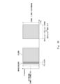
加算器114は、検出部111によりDL信号が検出された場合、そのDL信号がIFFT部112から出力された後、そのDL信号の時間域の前の時間域に、信号格納メモリ113に格納されたAMP安定化信号を加算する。このようにして、DL信号の時間域の前の時間域にAMP安定化信号を割り込ませる。このとき、加算器114は、DL信号のアンテナからの放射時間から、TX12の処理時間分を考慮して、DL信号が存在する時刻を逆算し、その時刻の先頭にAMP安定化信号を割り込ませる。図25は、DL信号の時間域の前の時間域に、AMP安定化信号を割り込ませた例を示す図である。
これにより、DL信号がTX12及び送信AMP13を通過する前に、AMP安定化信号をTX12及び送信AMP13を通過させることができる。
これにより、DL信号がTX12及び送信AMP13を通過する前に、AMP安定化信号をTX12及び送信AMP13を通過させることができる。
ここで、AAS10のTDD動作時には、DL信号の時間域の前の時間域は、例えば、TX12をOffからOnに切り替えるための期間であるTx On Transient periodとなる。そのため、AMP安定化信号の時間幅は、Tx On Transient periodの時間幅以内に設定される。Tx On Transient periodは、3GPP NRでは、10μsecに規定されている。
また、AMP安定化信号の周波数帯域幅は、DL信号の送信に使用するComponent Carrierの周波数帯域幅に設定される。
また、AMP安定化信号の電力レベルは、送信AMP13の出力が最大定格RMSレベルとなる電力レベルで、かつ、DL信号と同一の電力レベルに設定される。
また、AMP安定化信号の電力レベルは、送信AMP13の出力が最大定格RMSレベルとなる電力レベルで、かつ、DL信号と同一の電力レベルに設定される。
TX12は、信号処理部11の後段に設けられており、信号処理部11から出力されたDL信号又はAMP安定化信号を、IQ(In-Phase/Quadrature-Phase)信号からRF信号に変換して、送信AMP13に出力する。なお、TX12は、送受信機である不図示のTRX内に設けられる。また、TX12は、上述したように、DPPや、DPDの前段に設けられるCFR等を備えているが、これらの図示は省略されている。
送信AMP13は、TX12の後段に設けられており、TX12から出力されたDL信号又はAMP安定化信号を増幅して出力する。送信AMP13から出力されたDL信号又はAMP安定化信号は、不図示のアンテナを介して、各UEに送信される。
図26は、本実施の形態に係るAAS10の概略的な動作例を示すフローチャートである。図26に示されるように、検出部111は、DL信号の有無を検出する(ステップS11)。検出部111によりDL信号が検出された場合(ステップS12のYes)、加算器114は、DL信号の時間域の前の時間域にAMP安定化信号を割り込ませる(ステップS13)。そのため、まず、AMP安定化信号がTX12及び送信AMP13を通過し(ステップS14)、これにより、送信AMP13のGain、出力、及び非線形歪特性が安定化する。そして、その後に、DL信号がTX12及び送信AMP13を通過する(ステップS15)。
上述したように本実施の形態によれば、信号処理部11は、DL信号を検出した場合、DL信号の時間域の前の時間域に、AMP安定化信号を割り込ませ、DL信号がTX12及び送信AMP13を通過する前に、AMP安定化信号をTX12及び送信AMP13を通過させる。
このようにして、DL信号の先頭Symbolが送信AMP13に入力される前に、AMP安定化信号を送信AMP13に入力することによって、送信AMP13の電流コラプス及びGate/Drain Lagを早期に解消させる。これにより、送信AMP13の電流コラプス及びGate/Drain Lagに起因する特性変異を早期に収束させ、送信AMP13のGain、出力、AM-AM/AM-PM等の非線形歪特性を安定化させる。これにより、DL信号の先頭SymbolのEVMにOvershootが発生することを抑制でき、DL信号の先頭Symbolの通信品質を維持できる。その結果、DL信号の先頭SymbolのEVMのOvershootに起因する、多々の不具合の発生が回避されるため、DL信号の先頭SymbolやDL Slot中の任意の先頭Symbolから信号品質が保証される。また、DL信号の先頭Symbolが送信AMP13に入力された時点では、DL信号の先頭Symbol区間での送信AMP13のAM-AM/AM-PM特性が予め安定となっているため、DL信号の先頭Symbol及び以降のSymbolは、TX12内のDPDで安定的に歪補償される。このことも、DL信号が、先頭Symbolから、信号品質が保証されることに寄与する。
以下、本実施の形態の効果について、図面を参照して詳細に説明する。
図27は、Gate/Drain Lagが劣悪なGaN AMPである送信AMPを搭載し、AMP安定化信号の付与が無いAASにおいて、DL信号の振幅波形の例を示す図である。また、図28は、Gate/Drain Lagが劣悪なGaN AMPである送信AMP13を搭載し、送信AMP13にAMP安定化信号を付与する、本実施の形態に係るAAS10において、AMP安定化信号及びDL信号の振幅波形の例を示す図である。図27及び図28において、横軸は時間を示し、縦軸は振幅を示している。図27及び図28における振幅波形の差分は、後述する図29及び図30におけるEVMの特性の差分として現れることになる。
図27は、Gate/Drain Lagが劣悪なGaN AMPである送信AMPを搭載し、AMP安定化信号の付与が無いAASにおいて、DL信号の振幅波形の例を示す図である。また、図28は、Gate/Drain Lagが劣悪なGaN AMPである送信AMP13を搭載し、送信AMP13にAMP安定化信号を付与する、本実施の形態に係るAAS10において、AMP安定化信号及びDL信号の振幅波形の例を示す図である。図27及び図28において、横軸は時間を示し、縦軸は振幅を示している。図27及び図28における振幅波形の差分は、後述する図29及び図30におけるEVMの特性の差分として現れることになる。
図29は、Gate/Drain Lagが劣悪なGaN AMPである送信AMPを搭載し、AMP安定化信号の付与が無いAASにおいて、送信AMPをOnした時のEVMの特性の例を示す図である。また、図30は、Gate/Drain Lagが劣悪なGaN AMPである送信AMP13を搭載し、送信AMP13にAMP安定化信号を付与する、本実施の形態に係るAAS10において、送信AMP13をOnした時のEVMの特性の例を示す図である。図29及び図30において、横軸はSymbolを示し、縦軸はEVMを示している。なお、図29及び図30においては、送信AMPのOn/Offを1回のみ行っている。
図29に示されるように、Gate/Drain Lagが劣悪な送信AMPを搭載し、AMP安定化信号の付与が無いAASの場合、送信AMPをOnした直後のDL信号においては、先頭Symbol 1のEVMは、Overshootが発生しており、劣化している。これに対して、図30に示されるように、Gate/Drain Lagが劣悪な送信AMP13を搭載し、送信AMP13にAMP安定化信号を付与する、本実施の形態に係るAAS10の場合、送信AMP13をOnした直後のDL信号においては、先頭Symbol 1から、EVMは、Overshootが抑制されており、劣化していない。
図31は、Gate/Drain Lagが劣悪なGaN AMPである送信AMP13を搭載し、送信AMP13にAMP安定化信号を付与する、本実施の形態に係るAAS10において、送信AMP13をOnした直後のDL信号の先頭Symbol 1のコンスタレーションの例を示す図である。なお、Gate/Drain Lagが劣悪な送信AMPを搭載し、AMP安定化信号の付与が無いAASにおいて、送信AMPをOnした直後のDL信号の先頭Symbol 1のコンスタレーションの例は、図11に示したものと同様である。
図11に示されるように、Gate/Drain Lagが劣悪な送信AMPを搭載し、AMP安定化信号の付与が無いAASの場合、送信AMPをOnした直後のDL信号の先頭Symbol 1のコンスタレーションは、位相回転が発生している。これに対して、図31に示されるように、Gate/Drain Lagが劣悪な送信AMP13を搭載し、送信AMP13にAMP安定化信号を付与する、本実施の形態に係るAAS10の場合、送信AMPをOnした直後のDL信号は、先頭Symbol 1からコンスタレーションが正常である。
図32は、Gate/Drain Lagが劣悪なGaN AMPである送信AMP13を搭載し、送信AMP13にAMP安定化信号を付与する、本実施の形態に係るAAS10において、複数のMCSの各々について、SNRとThroughputとの関係の例を示す図である。図32において、横軸はSNRを示し、縦軸はThroughputを示している。なお、Gate/Drain Lagが劣悪な送信AMPを搭載し、AMP安定化信号の付与が無いAASにおいて、複数のMCSの各々について、SNRとThroughputとの関係の例は、図13に示したものと同様である。
図13に示されるように、Gate/Drain Lagが劣悪な送信AMPを搭載し、AMP安定化信号の付与が無いAASの場合、特に、MCSの最大方向(高次QAM)側では、SNRに応じたMax Throughputが達成できなくなる。そのため、SNRが約20dB以上のMCSが、運用できなくなってしまう。これに対して、図32に示されるように、Gate/Drain Lagが劣悪なGaN AMPである送信AMP13を搭載し、送信AMP13にAMP安定化信号を付与する、本実施の形態に係るAAS10の場合、最大のMCSまで、SNRに応じたMax Throughputが達成できるようになる。
以上、実施の形態を参照して本開示について説明したが、本開示は上述した実施の形態に限定されるものではない。本開示の構成や詳細には、本開示のスコープ内で当業者が理解し得る様々な変更をすることができる。
例えば、上述した実施の形態では、本開示に係る無線通信装置をAASに用いる例について説明したが、本開示は、これに限定されるものではない。本開示に係る無線通信装置は、送信信号を送信する送信機能を備えた任意の無線通信装置(例えば、Wide Area向け基地局、マクロ基地局等)に用いることが可能である。
また、本開示に係る無線通信装置の一部の機能を、CPU(Central Processing Unit)等のプロセッサにプログラムを実行させることにより実現することも可能である。
図33は、本開示に係る無線通信装置の一部の機能を実現するコンピュータ20のハードウェア構成例を示す図である。
図33に示されるように、コンピュータ20は、プロセッサ21及びメモリ22を備えている。
図33は、本開示に係る無線通信装置の一部の機能を実現するコンピュータ20のハードウェア構成例を示す図である。
図33に示されるように、コンピュータ20は、プロセッサ21及びメモリ22を備えている。
プロセッサ21は、例えば、マイクロプロセッサ、CPU又はMPU(Micro Processing Unit)、又はであっても良い。プロセッサ21は、複数のプロセッサを含んでも良い。
メモリ22は、揮発性メモリ及び不揮発性メモリの組み合わせによって構成される。メモリ22は、プロセッサ21から離れて配置されたストレージを含んでも良い。この場合、プロセッサ21は、図示されていないI(Input)/O(Output)インタフェースを介してメモリ22にアクセスしても良い。
メモリ22には、プログラムが記憶される。このプログラムは、コンピュータ20に読み込まれた場合に、上述した実施の形態に係るAAS10の一部の機能をコンピュータ20に行わせるための命令群(又はソフトウェアコード)を含む。上述したAAS10における構成要素は、プロセッサ21がメモリ22に記憶されたプログラムを読み込んで実行することにより実現されても良い。また、上述したAAS10における記憶機能を備える構成要素は、メモリ22により実現されても良い。
また、上述したプログラムは、非一時的なコンピュータ可読媒体又は実体のある記憶媒体に格納されても良い。限定ではなく例として、コンピュータ可読媒体又は実体のある記憶媒体は、random-access memory(RAM)、read-only memory(ROM)、フラッシュメモリ、solid-state drive(SSD)又はその他のメモリ技術、CD-ROM、digital versatile disc(DVD)、Blu-ray(登録商標)ディスク又はその他の光ディスクストレージ、磁気カセット、磁気テープ、磁気ディスクストレージ又はその他の磁気ストレージデバイスを含む。プログラムは、一時的なコンピュータ可読媒体又は通信媒体上で送信されても良い。限定ではなく例として、一時的なコンピュータ可読媒体又は通信媒体は、電気的、光学的、音響的、又はその他の形式の伝搬信号を含む。
10 AAS
11 信号処理部
111 検出部
112 IFFT部
113 信号格納メモリ
114 加算器
12 TX
13 送信AMP
20 コンピュータ
21 プロセッサ
22 メモリ
11 信号処理部
111 検出部
112 IFFT部
113 信号格納メモリ
114 加算器
12 TX
13 送信AMP
20 コンピュータ
21 プロセッサ
22 メモリ
Claims (8)
- 信号処理部と、
前記信号処理部の後段に設けられた送信機と、
前記送信機の後段に設けられた送信アンプと、を備え、
前記信号処理部は、
送信信号の有無を検出し、
前記送信信号を検出した場合、前記送信アンプの特性を安定化させるための安定化信号を、前記送信信号の時間域の前の時間域に割り込ませることで、前記送信信号が前記送信機及び前記送信アンプを通過する前に、前記安定化信号を前記送信機及び前記送信アンプを通過させる、
無線通信装置。 - 前記信号処理部は、
前記安定化信号を格納する信号格納メモリと、
前記送信信号を、周波数領域の信号から時間領域の信号に変換するIFFT(Inverse Fast Fourier Transform)部と、
前記IFFT部の前段に設けられ、周波数領域において、前記送信信号の有無を検出する検出部と、
前記検出部により前記送信信号が検出された場合、前記IFFT部から出力された前記送信信号の時間域の前の時間域に、前記信号格納メモリに格納された前記安定化信号を加算する加算器と、を備える、
請求項1に記載の無線通信装置。 - 前記無線通信装置がTDD(Time Division Duplex)動作を行う場合、前記安定化信号の時間幅は、前記送信機をOffからOnに切り替えるための期間の時間幅以内に設定される、
請求項1に記載の無線通信装置。 - 前記安定化信号の周波数帯域幅は、前記送信信号の送信に使用するコンポーネントキャリアの周波数帯域幅に設定される、
請求項1に記載の無線通信装置。 - 前記安定化信号の電力レベルは、前記送信アンプの出力が最大定格RMS(Root Mean Square)レベルとなる電力レベルで、かつ、前記送信信号と同一の電力レベルに設定される、
請求項1に記載の無線通信装置。 - 前記安定化信号は、前記送信アンプに入力されると、前記送信アンプに電流コラプス及びゲイン/ドレインラグを発生させて、前記送信アンプのゲイン、出力、及び非線形歪特性を安定化させる信号である、
請求項1に記載の無線通信装置。 - 前記送信アンプは、GaN FET(Field Effect Transistor)を用いるアンプである、
請求項1から6のいずれか1項に記載の無線通信装置。 - 送信機と、前記送信機の後段に設けられた送信アンプと、を備える無線通信装置により実行される無線通信方法であって、
前記送信アンプの前段で送信信号の有無を検出するステップと、
前記送信信号を検出した場合、前記送信アンプの特性を安定化させるための安定化信号を、前記送信信号の時間域の前の時間域に割り込ませることで、前記送信信号が前記送信機及び前記送信アンプを通過する前に、前記安定化信号を前記送信機及び前記送信アンプを通過させるステップと、を含む、
無線通信方法。
Priority Applications (1)
| Application Number | Priority Date | Filing Date | Title |
|---|---|---|---|
| PCT/JP2022/016155 WO2023188161A1 (ja) | 2022-03-30 | 2022-03-30 | 無線通信装置及び無線通信方法 |
Applications Claiming Priority (1)
| Application Number | Priority Date | Filing Date | Title |
|---|---|---|---|
| PCT/JP2022/016155 WO2023188161A1 (ja) | 2022-03-30 | 2022-03-30 | 無線通信装置及び無線通信方法 |
Publications (1)
| Publication Number | Publication Date |
|---|---|
| WO2023188161A1 true WO2023188161A1 (ja) | 2023-10-05 |
Family
ID=88199714
Family Applications (1)
| Application Number | Title | Priority Date | Filing Date |
|---|---|---|---|
| PCT/JP2022/016155 WO2023188161A1 (ja) | 2022-03-30 | 2022-03-30 | 無線通信装置及び無線通信方法 |
Country Status (1)
| Country | Link |
|---|---|
| WO (1) | WO2023188161A1 (ja) |
Citations (3)
| Publication number | Priority date | Publication date | Assignee | Title |
|---|---|---|---|---|
| JPH02116769A (ja) * | 1988-10-27 | 1990-05-01 | Tech Res & Dev Inst Of Japan Def Agency | パルス送信装置 |
| WO2012111274A1 (ja) * | 2011-02-14 | 2012-08-23 | パナソニック株式会社 | 高周波電力増幅器 |
| JP2021121054A (ja) * | 2020-01-30 | 2021-08-19 | 国立研究開発法人宇宙航空研究開発機構 | 増幅装置、送受信システム |
-
2022
- 2022-03-30 WO PCT/JP2022/016155 patent/WO2023188161A1/ja unknown
Patent Citations (3)
| Publication number | Priority date | Publication date | Assignee | Title |
|---|---|---|---|---|
| JPH02116769A (ja) * | 1988-10-27 | 1990-05-01 | Tech Res & Dev Inst Of Japan Def Agency | パルス送信装置 |
| WO2012111274A1 (ja) * | 2011-02-14 | 2012-08-23 | パナソニック株式会社 | 高周波電力増幅器 |
| JP2021121054A (ja) * | 2020-01-30 | 2021-08-19 | 国立研究開発法人宇宙航空研究開発機構 | 増幅装置、送受信システム |
Similar Documents
| Publication | Publication Date | Title |
|---|---|---|
| EP2909931B1 (en) | Envelope tracking distributed amplifier | |
| US11374538B2 (en) | Apparatus and methods for envelope tracking | |
| US11881818B2 (en) | Envelope tracking for Doherty power amplifiers | |
| JP6567655B2 (ja) | 無線周波数(rf)電力増幅器回路とrf電力増幅器バイアス回路 | |
| TWI575866B (zh) | 校正在波封為基追蹤系統中之不變功率放大器負載特性的方法與裝置 | |
| KR102059138B1 (ko) | 포락선 추적 보정 장치 및 방법 | |
| EP3130075B1 (en) | Circuits and methods for biasing a power amplifier | |
| US10003310B1 (en) | Segmented digital predistortion apparatus and methods | |
| WO2010084544A1 (ja) | 高周波増幅器、無線装置及び制御方法 | |
| Saad et al. | The continuum of load modulation ratio from Doherty to traveling-wave amplifiers | |
| US20160227549A1 (en) | Radio device that has function to reduce peak power of multiplexed signal | |
| US11368175B2 (en) | Radio frequency control circuit | |
| EP3309959B1 (en) | Amplification system and enodeb | |
| JP2007522746A (ja) | 減少した消費電力を有する無線送信機 | |
| WO2023188161A1 (ja) | 無線通信装置及び無線通信方法 | |
| US20140010330A1 (en) | Transmission device and transmission method | |
| Nair et al. | A comparative study on digital predistortion techniques for Doherty amplifier for LTE applications | |
| Singh et al. | Design and performance analysis of broadband Doherty power amplifier for 5G communication system | |
| Shah et al. | Power-efficient LTE MACRO eNodeB: A comprehensive survey | |
| US20240089877A1 (en) | Wireless communication apparatus, wireless communication system, and wireless communication method | |
| Hussaini et al. | Optimum design of Doherty RFPA for mobile WiMAX base stations | |
| US20230126040A1 (en) | Power amplifier linearity control based on power amplifier operating mode or power level | |
| US11973468B2 (en) | Apparatus and methods for envelope tracking | |
| US20230396219A1 (en) | Signal amplification circuitry | |
| US20220360291A1 (en) | Efficient amplifer operation |
Legal Events
| Date | Code | Title | Description |
|---|---|---|---|
| 121 | Ep: the epo has been informed by wipo that ep was designated in this application |
Ref document number: 22935306 Country of ref document: EP Kind code of ref document: A1 |