WO2023188161A1 - Dispositif de communication sans fil et procédé de communication sans fil - Google Patents
Dispositif de communication sans fil et procédé de communication sans fil Download PDFInfo
- Publication number
- WO2023188161A1 WO2023188161A1 PCT/JP2022/016155 JP2022016155W WO2023188161A1 WO 2023188161 A1 WO2023188161 A1 WO 2023188161A1 JP 2022016155 W JP2022016155 W JP 2022016155W WO 2023188161 A1 WO2023188161 A1 WO 2023188161A1
- Authority
- WO
- WIPO (PCT)
- Prior art keywords
- signal
- transmission
- transmitting
- wireless communication
- transmitter
- Prior art date
Links
- 238000004891 communication Methods 0.000 title claims description 43
- 238000000034 method Methods 0.000 title claims description 11
- 230000005540 biological transmission Effects 0.000 claims abstract description 145
- 230000006641 stabilisation Effects 0.000 claims abstract description 76
- 238000011105 stabilization Methods 0.000 claims abstract description 76
- 230000000087 stabilizing effect Effects 0.000 claims abstract description 14
- 238000001514 detection method Methods 0.000 claims description 10
- 230000005669 field effect Effects 0.000 claims description 2
- 229920006227 ethylene-grafted-maleic anhydride Polymers 0.000 description 319
- 238000010586 diagram Methods 0.000 description 55
- 229910002704 AlGaN Inorganic materials 0.000 description 17
- 230000001052 transient effect Effects 0.000 description 16
- 230000006870 function Effects 0.000 description 6
- 230000008859 change Effects 0.000 description 5
- 230000007423 decrease Effects 0.000 description 5
- 230000003071 parasitic effect Effects 0.000 description 5
- 239000000758 substrate Substances 0.000 description 5
- 230000004044 response Effects 0.000 description 4
- 125000003345 AMP group Chemical group 0.000 description 3
- 230000003044 adaptive effect Effects 0.000 description 3
- 230000003321 amplification Effects 0.000 description 3
- 239000013078 crystal Substances 0.000 description 3
- 238000003199 nucleic acid amplification method Methods 0.000 description 3
- 239000004065 semiconductor Substances 0.000 description 3
- 229910001218 Gallium arsenide Inorganic materials 0.000 description 2
- 230000008901 benefit Effects 0.000 description 2
- 230000003287 optical effect Effects 0.000 description 2
- 238000011084 recovery Methods 0.000 description 2
- 230000005533 two-dimensional electron gas Effects 0.000 description 2
- 238000004458 analytical method Methods 0.000 description 1
- 125000004429 atom Chemical group 0.000 description 1
- 239000000969 carrier Substances 0.000 description 1
- 230000015556 catabolic process Effects 0.000 description 1
- 150000001875 compounds Chemical class 0.000 description 1
- 125000004122 cyclic group Chemical group 0.000 description 1
- 230000003247 decreasing effect Effects 0.000 description 1
- 230000003111 delayed effect Effects 0.000 description 1
- 238000007599 discharging Methods 0.000 description 1
- 230000000694 effects Effects 0.000 description 1
- 238000005516 engineering process Methods 0.000 description 1
- 239000000284 extract Substances 0.000 description 1
- GVVPGTZRZFNKDS-JXMROGBWSA-N geranyl diphosphate Chemical compound CC(C)=CCC\C(C)=C\CO[P@](O)(=O)OP(O)(O)=O GVVPGTZRZFNKDS-JXMROGBWSA-N 0.000 description 1
- 125000004435 hydrogen atom Chemical group [H]* 0.000 description 1
- 230000006872 improvement Effects 0.000 description 1
- 239000012535 impurity Substances 0.000 description 1
- 230000007774 longterm Effects 0.000 description 1
- 239000000463 material Substances 0.000 description 1
- 230000003446 memory effect Effects 0.000 description 1
- 125000004430 oxygen atom Chemical group O* 0.000 description 1
- 230000010363 phase shift Effects 0.000 description 1
- 230000000704 physical effect Effects 0.000 description 1
- 230000001902 propagating effect Effects 0.000 description 1
- 230000005855 radiation Effects 0.000 description 1
- 230000008707 rearrangement Effects 0.000 description 1
- 230000009467 reduction Effects 0.000 description 1
- 229910052594 sapphire Inorganic materials 0.000 description 1
- 239000010980 sapphire Substances 0.000 description 1
- 238000001179 sorption measurement Methods 0.000 description 1
- 238000001228 spectrum Methods 0.000 description 1
- 230000007480 spreading Effects 0.000 description 1
- -1 surface levels Substances 0.000 description 1
Images


Classifications
-
- H—ELECTRICITY
- H04—ELECTRIC COMMUNICATION TECHNIQUE
- H04B—TRANSMISSION
- H04B1/00—Details of transmission systems, not covered by a single one of groups H04B3/00 - H04B13/00; Details of transmission systems not characterised by the medium used for transmission
- H04B1/02—Transmitters
- H04B1/04—Circuits
Definitions
- the present disclosure relates to a wireless communication device and a wireless communication method.
- GaN Compared to GaAs, GaN has advantages in that it has a large band gap energy, high breakdown voltage, can be miniaturized, and high electron mobility. Therefore, RF (Radio Frequency) devices such as transmitter AMPs that use GaN FETs (Field Effect Transistors) have higher output power than RF devices that use GaAs FETs, and are suitable for wide area base stations, macro base stations, and AAS ( It continues to be adopted in wireless communication devices such as Antenna Active System). Additionally, the two-dimensional electron gas structure of GaN/AlGaN FETs has physical properties such as higher mobility compared to Si FETs.
- RF Radio Frequency
- GaN/AlGaN FETs have been adopted and put into practical use, especially as high-output RF devices in the high frequency band of RF.
- An example of a GaN/AlGaN FET is a GaN/AlGaN HEMT (High Electron Mobility Transistor).
- FIG. 1 is a diagram showing an example of the structure of a GaN/AlGaN HEMT.
- FIG. 2 is a diagram showing an example of the band structure of GaN/AlGaN HEMT.
- GaN/AlGaN HEMTs are realized by growing GaN/AlGaN on a sapphire substrate.
- GaN/AlGaN HEMTs use an electron layer called a two-dimensional electron gas generated at the boundary between different compound materials as carriers, and the electron supply layer (AlGaN layer) and electron transit layer (GaN layer) are different. Therefore, GaN/AlGaN HEMTs have the advantage that they can achieve high electron mobility, can be used at high speeds and high frequencies, and can output large amounts of power with high efficiency.
- a phenomenon called current collapse is a phenomenon in which drain current decreases as drain voltage is applied.
- current collapse it is described in Patent Document 1, for example.
- the increase or decrease in drain current is an unstable factor (memory effect) such as the current gain and output decreasing or fluctuating depending on the history of past amplitude amplification operations, and is caused by DPD (Digital Pre-Distortion). This increases the difficulty level of distortion improvement.
- Drain Lag and Gate Lag also pose a problem in the transmission AMP.
- class C amplification begins when a drain current flows in response to the amplitude of the transmitting signal exceeding a certain level, and a matching circuit (including the amplified signal as the fundamental wave) that matches the output of the transmitting AMP
- a fundamental amplified signal is output by a tank circuit that extracts and outputs only the fundamental wave from the harmonic group amplified signal.
- Drain Lag is a phenomenon in which when the drain voltage is suddenly turned off to on to enable amplifying operation of the transmitting AMP, the drain current changes transiently and slowly until it reaches a steady voltage state.
- a wireless communication device equipped with a transmitting AMP turns the transmitting AMP off and on when switching between UL (Up Link) and DL (Down Link).
- the desired Ids are set and the transmitting AMP turns on, but at that time a sudden change in gate voltage occurs.
- Gate Lag is a state where the drain current is in a steady voltage state in response to a sudden change in gate voltage (Ids Off with Gate Pinch-Off, transmitting AMP is completely off ⁇ sudden change to gate voltage that sets Ids of transmitting AMP On). It is a phenomenon that changes transiently and slowly until it reaches .
- These Gate Lag and Drain Lag (hereinafter referred to as "Gate/Drain Lag" as appropriate) are also used when the transmission AMP using AlGaN/GaN HEMT performs high-speed Off/On operation and burst operation to perform TDD operation. This results in failure of transient response delay until normal state is reached.
- a normal state means that nonlinear distortion characteristics such as gain, output, AM (Amplitude Modulation)-AM/AM-PM (Phase Modulation), etc. are in a steady state.
- LTE Long Term Evolution
- 5G Fifth Generation Partnership Project
- base stations perform burst operations that turn the transmitting AMP on and off over time, and transmit data according to the transmitting symbol.
- Adaptive control for low power consumption is performed by frequently turning AMP on and off. At that time, due to the transient response delay described above, it was necessary to significantly advance the On control of the transmitting AMP, and it took a long time to stabilize the transmitting signal.
- GaN AMP an AMP using a GaN FET
- the wireless communication device equipped with the transmission AMP is an AAS that transmits a DL signal as a transmission signal to each UE (User Equipment: mobile terminal).
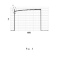
- FIG. 3 is a diagram showing an example of the characteristics of the drain current Ids when the gate is turned on from the pinch-off state in a transmission AMP that is a GaN AMP.
- the horizontal axis shows time
- the vertical axis shows drain current Ids.
- FIG. 4 is an enlarged view of the X portion of FIG. 3.
- FIG. 4 shows the characteristics of Ids when the Vgs setting is changed in four ways.
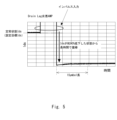
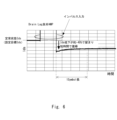
- FIG. 5 shows an example of how the characteristics of the drain current Ids when an impulse is input to a transmitting AMP, which is a GaN AMP with poor drain lag, decreases from the steady setting Ids state value before the impulse is applied. It is a diagram. Further, FIG. 6 is a diagram showing an example of the characteristics of the drain current Ids when an impulse is input to a transmission AMP that is a GaN AMP with a good drain lag. Furthermore, in FIGS. 5 and 6, the horizontal axis represents time, and the vertical axis represents drain current Ids.
- the length of one symbol when Sub Carrier Space is 15kHz is approximately 64 ⁇ sec. Furthermore, in 5G, the length of one symbol when Sub Carrier Space is 30kHz is approximately 36 ⁇ sec, which is approximately half of the length of one symbol of LTE described above.
- the drain current Ids can be returned to the desired Ids within 1 symbol length after inputting the impulse, regardless of whether it is LTE or 5G.
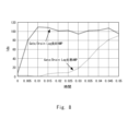
- FIG. 7 is a diagram showing an example of the characteristics of the drain current Ids when a transmission AMP with a good Gate/Drain Lag is a GaN AMP and a transmission AMP with a poor Gate/Drain Lag is turned on.
- the horizontal axis shows time
- the vertical axis shows drain current Ids.
- FIG. 8 is an enlarged view of the X portion of FIG. 7. Note that in FIGS. 7 and 8, no RF modulation signal is input to the transmitting AMP.
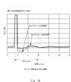
- FIG. 9 is a diagram showing an example of EVM (Error Vector Magnitude) characteristics when the transmitting AMP is turned on in an AAS equipped with a transmitting AMP that is a GaN AMP with poor Gate/Drain Lag.
- FIG. 10 is a diagram showing an example of EVM characteristics when the transmission AMP is turned on in an AAS equipped with a transmission AMP that is a GaN AMP with good Gate/Drain Lag.
- the horizontal axis represents symbols
- the vertical axis represents EVM. Note that in FIGS. 9 and 10, the transmission AMP is turned on and off twice.
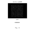
- FIG. 11 is a diagram showing an example of the constellation of Symbol 1 at the beginning of the DL signal immediately after the transmission AMP is turned on in an AAS equipped with a transmission AMP that is a GaN AMP with poor Gate/Drain Lag.
- FIG. 12 is a diagram showing an example of the constellation of the first Symbol 1 of the DL signal immediately after the transmission AMP is turned on in an AAS equipped with a transmission AMP that is a GaN AMP with good Gate/Drain Lag.
- FIG. 13 shows the relationship between SNR (Signal-to-Noise Ratio) and Throughput for each of multiple MCS (Modulation and channel Coding Schemes) in an AAS equipped with a transmission AMP that is a GaN AMP with poor Gate/Drain Lag.
- FIG. 3 is a diagram showing an example of a relationship.
- FIG. 14 is a diagram showing an example of the relationship between SNR and Throughput for each of a plurality of MCSs in an AAS equipped with a transmission AMP that is a GaN AMP with good Gate/Drain Lag.
- the horizontal axis shows SNR
- the vertical axis shows Throughput.
- an object of the present disclosure is to provide a wireless communication device and a wireless communication method that can maintain the communication quality of the leading portion of a transmission signal.
- a wireless communication device includes: a signal processing section; a transmitter provided after the signal processing section; a transmission amplifier provided after the transmitter,
- the signal processing section includes: Detects the presence or absence of a transmitted signal, When the transmitted signal is detected, a stabilizing signal for stabilizing the characteristics of the transmitting amplifier is inserted into a time domain before the time domain of the transmitted signal, so that the transmitted signal can be detected by the transmitter and the transmitter.
- the stabilized signal is passed through the transmitter and the transmit amplifier before passing through the transmit amplifier.
- a wireless communication method includes: A wireless communication method performed by a wireless communication device including a transmitter and a transmission amplifier provided at a stage subsequent to the transmitter, the method comprising: detecting the presence or absence of a transmission signal at a stage before the transmission amplifier; When the transmission signal is detected, a stabilizing signal for stabilizing the characteristics of the transmission amplifier is inserted into a time domain before the time domain of the transmission signal, so that the transmission signal is transmitted to the transmitter and the transmitter. passing the stabilized signal through the transmitter and the transmit amplifier before passing through the transmit amplifier.
- FIG. 3 is a diagram showing an example of the structure of a GaN/AlGaN HEMT.
- FIG. 3 is a diagram showing an example of a band structure of GaN/AlGaN HEMT.
- FIG. 7 is a diagram showing an example of the characteristics of the drain current Ids when the gate is turned on from a pinch-off state in a transmission AMP that is a GaN AMP. 4 is an enlarged view of the X portion of FIG. 3.
- FIG. FIG. 7 is a diagram showing an example of the characteristics of drain current Ids when an impulse is input to a transmission AMP that is a GaN AMP with poor drain lag.
- FIG. 1 is a diagram showing an example of the structure of a GaN/AlGaN HEMT.
- FIG. 3 is a diagram showing an example of a band structure of GaN/AlGaN HEMT.
- FIG. 7 is a diagram showing an example of the characteristics of the drain current Ids when
- FIG. 7 is a diagram showing an example of the characteristics of drain current Ids when an impulse is input to a transmission AMP that is a GaN AMP with good drain lag.
- FIG. 7 is a diagram showing an example of the characteristics of the drain current Ids when a transmission AMP that is a GaN AMP with good Gate/Drain Lag and a transmission AMP that is a GaN AMP with poor Gate/Drain Lag are respectively turned on.
- 8 is an enlarged view of the X portion of FIG. 7.
- FIG. FIG. 7 is a diagram showing an example of EVM characteristics when the transmission AMP is turned on in an AAS equipped with a transmission AMP that is a GaN AMP with poor Gate/Drain Lag.
- FIG. 7 is a diagram showing an example of EVM characteristics when the transmitting AMP is turned on in an AAS equipped with a transmitting AMP that is a GaN AMP with good Gate/Drain Lag.
- an AAS equipped with a transmission AMP that is a GaN AMP with poor Gate/Drain Lag it is a diagram showing an example of the constellation of the first symbol of a DL signal immediately after the transmission AMP is turned on.
- FIG. 3 is a diagram showing an example of a constellation of the first symbol of a DL signal immediately after the transmission AMP is turned on in an AAS equipped with a transmission AMP that is a GaN AMP with good Gate/Drain Lag.
- FIG. 3 is a diagram showing an example of a constellation of the first symbol of a DL signal immediately after the transmission AMP is turned on in an AAS equipped with a transmission AMP that is a GaN AMP with good Gate/Drain Lag.
- FIG. 7 is a diagram illustrating an example of the relationship between SNR and Throughput for each of a plurality of MCSs in an AAS equipped with a transmission AMP that is a GaN AMP with poor Gate/Drain Lag.
- FIG. 7 is a diagram showing an example of the relationship between SNR and Throughput for each of a plurality of MCSs in an AAS equipped with a transmission AMP that is a GaN AMP with good Gate/Drain Lag.
- Characteristics of the drain current Ids in a state where no RF modulation signal is input when the transmission AMP with a GaN AMP with a good Gate/Drain Lag and the transmission AMP with a GaN AMP with a poor Gate/Drain Lag are turned on.
- FIG. 7 is a diagram showing an example of the characteristics of the deviation of drain current Ids when RF modulation signals having different input levels are input after turning on a transmission AMP that is a GaN AMP with poor Gate/Drain Lag.
- FIG. 7 is a diagram showing an example of the arrangement of AMP stabilization signals in the time direction, frequency direction, and power direction.
- FIG. 3 is a diagram showing an example of arrangement of AMP stabilization signals in the frequency direction and power direction.
- FIG. 7 is a diagram showing an example of the arrangement of AMP stabilization signals in the time direction and frequency direction.
- FIG. 3 is a diagram showing an example of a data structure of an AMP stabilization signal.
- FIG. 3 is a diagram showing an example of time arrangement of AMP stabilization signals.
- 7 is a timing chart showing an example of a change in processing start timing due to an interrupt of an AMP stabilization signal in AAS.
- FIG. 2 is a diagram illustrating a configuration example of an AAS according to an embodiment.
- FIG. 7 is a diagram showing an example in which an AMP stabilization signal is inserted into the time domain before the time domain of the DL signal in the AAS according to the embodiment.
- FIG. 3 is a flowchart illustrating a schematic operation example of AAS according to an embodiment.
- FIG. 7 is a diagram showing an example of the amplitude waveform of a DL signal in an AAS equipped with a transmission AMP that is a GaN AMP with poor Gate/Drain Lag and no AMP stabilization signal provided.
- An example of the amplitude waveform of an AMP stabilization signal and a DL signal is shown in an AAS according to an embodiment that is equipped with a transmission AMP that is a GaN AMP with poor Gate/Drain Lag and provides an AMP stabilization signal to the transmission AMP. It is a diagram.
- FIG. 7 is a diagram showing an example of the amplitude waveform of a DL signal in an AAS equipped with a transmission AMP that is a GaN AMP with poor Gate/Drain Lag and provides an AMP stabilization signal to the transmission AMP.
- FIG. 7 is a diagram showing an example of EVM characteristics when the transmitting AMP is turned on in an AAS equipped with a transmitting AMP that is a GaN AMP with poor Gate/Drain Lag and no AMP stabilization signal provided.
- An example of EVM characteristics when the transmission AMP is turned on in an AAS according to an embodiment that is equipped with a transmission AMP that is a GaN AMP with poor Gate/Drain Lag and provides an AMP stabilization signal to the transmission AMP is shown. It is a diagram.
- FIG. 2 is a diagram illustrating an example hardware configuration of a computer that implements some functions of a wireless communication device according to the present disclosure.
- the wireless communication device equipped with the transmission AMP is an AAS that transmits a DL signal as a transmission signal to each UE.
- the inventor of the present disclosure found that even in a transmitting AMP with poor Gate/Drain Lag, inputting an RF modulation signal after inputting an impulse can shorten the time it takes for the characteristics of the transmitting AMP to stabilize. .
- FIG. 15 shows the drain current in a state where no RF modulation signal is input when the transmission AMP with a GaN AMP with a good Gate/Drain Lag and the transmission AMP with a GaN AMP with a poor Gate/Drain Lag are turned on.
- FIG. 3 is a diagram showing an example of characteristics of Ids.
- the horizontal axis shows time
- the vertical axis shows drain current Ids.
- Figure 16 shows the gain when an RF modulation signal is input together with an impulse for a transmitting AMP that is a GaN AMP with good Gate/Drain Lag and a transmitting AMP that is a GaN AMP with poor Gate/Drain Lag.
- FIG. 2 is a diagram showing an example of the characteristics of In FIG. 16, the horizontal axis shows time and the vertical axis shows Gain.
- the drain current Ids rises slowly immediately after the transmission AMP is turned on when no RF modulation signal is input. Therefore, although not shown in FIG. 15, a long time of approximately 80 ⁇ sec is required until the drain current Ids is restored to the desired Ids.
- the length of one symbol when Sub Carrier Space is 30kHz is approximately 36 ⁇ sec. Therefore, the approximately 80 ⁇ sec required for the drain current Ids to recover corresponds to approximately 2 Symbol lengths of the 5G described above.
- the inventor of the present disclosure has found that even in a transmitting AMP with poor Gate/Drain Lag, the characteristics of the transmitting AMP are stabilized when the input level of the RF modulation signal input to the transmitting AMP is higher after the transmitting AMP is turned on. We have found that it is possible to shorten the time it takes.
- FIG. 17 is a diagram showing an example of the characteristics of the deviation of drain current Ids when RF modulation signals with different input levels are input after turning on a transmitting AMP that is a GaN AMP with poor Gate/Drain Lag. .
- the horizontal axis shows time
- the vertical axis shows the deviation of drain current Ids.
- Idq inle current when no signal is set
- Ids 90mA
- Ids equals 90 mA before inputting the transmission signal.
- the drain current Ids is fixed at 90 mA, and the input level of the RF modulation signal is varied within the range of 33.7 dBm to 45.7 dBm.
- each operating CC Component Carrier setting
- the AMP stabilization signal is inserted into the time domain immediately before the time domain of the DL signal.
- the AM-AM/AM-PM characteristics of the transmitting AMP in the first symbol section of the DL signal are already stable, so the first symbol of the DL signal and subsequent Symbols are stably compensated for distortion by the DPD in the TX, which is the transmitter. This also contributes to ensuring the signal quality of the DL signal from the first Symbol.
- TX is provided within TRX, which is a transmitter/receiver.
- FIG. 18 is a diagram showing an example of the arrangement of the AMP stabilization signal in the time direction, frequency direction, and power direction.
- FIG. 19 is a diagram showing an example of arrangement of the AMP stabilization signal in the frequency direction and the power direction.
- FIG. 20 is a diagram showing an example of the arrangement of the AMP stabilization signal in the time direction and frequency direction. Note that in FIGS. 18 to 20, it is assumed that the DL signal is a signal for each slot or a signal for each symbol.
- the AMP stabilization signal is, for example, a signal in OFDM (Orthogonal Frequency Division Multiplexing) Format.
- the AMP stabilized signal is a signal having an amplitude probability density of a Reighley distribution with a PAPR (Peak to Average Power Ratio) of 14 dB.
- the AMP stabilized signal passes through the CFR (Crest Factor Reduction) placed before the DPD in the TX, and then the PAPR of the AMP stabilized signal is soft clipped to the CFR threshold (about 7 to 8 dB). be done.
- CFR Rest Factor Reduction
- the AMP stabilization signal is placed in the time area before the first Symbol of the DL Slot or any Symbol in the DL Slot.
- a transient period called a Tx On Transient period is set as a period for switching TX from Off to On. Therefore, in the situation under TDD system, the AMP stabilization signal will be placed in the time domain within the Tx On Transient period before the DL signal.
- the Tx On Transient period is specified as 10 ⁇ sec. .
- the time width of the signal obtained by adding Ramp Up/Down to the AMP stabilization signal is set to within 10 ⁇ s.
- Ramp Up/Down is a signal inserted to prevent impulse spectrum spreading.
- the time width of the DL signal is approximately 36 ⁇ sec to several DL slots.
- the time width of the DL signal is 140 ⁇ sec when operating in SSB (SS (Synchronization Signal)/PBCH (Physical Broadcast CHannel) Block).
- SSB is a synchronization signal/broadcast channel block composed of SS and PBCH.
- SSB is sent periodically from base stations mainly for terminals to detect cell ID and reception timing when starting communication, but in 5G NR it is also used to measure the reception quality of each cell.
- the frequency bandwidth of the AMP stabilization signal is set to a wide band equivalent to the frequency bandwidth of each Component Carrier used for transmitting the DL signal.
- the frequency bandwidth of each Component Carrier is approximately 20MHz to 100MHz.
- the frequency bandwidth of the DL signal is approximately 7.2 MHz when operating in SSB, and the frequency bandwidth of each Component Carrier under actual DL signals such as PDSCH (Physical Downlink Shared CHannel).
- increasing the input level of the RF modulation signal further promotes early recovery of the characteristics of the transmitting AMP. Therefore, the power level of the AMP stabilization signal is set to a high level at which the output of the transmitting AMP reaches the maximum rated RMS (Root Mean Square) level and the same power level as the DL signal.
- the AMP stabilization signal is Pass the stabilized signal through the transmitting AMP.
- the AM-AM/AM-PM characteristics of the transmitting AMP in the first symbol section of the DL signal are already stable, so the first symbol of the DL signal and subsequent Symbols are stably compensated for distortion by DPD in TX. This also contributes to ensuring the signal quality of the DL signal from the first Symbol.
- the AMP stabilization signal is placed in the time domain within the Tx On Transient period before the DL signal, but in 3GPP NR, the Tx On Transient period is defined as 10 ⁇ sec. Therefore, within 10 ⁇ s of the Tx On Transient period, the nonlinear distortion characteristics such as AM-PM of the transmitting AMP are stabilized, and then the DL signal is subjected to distortion compensation by DPD.
- FIG. 21 is a diagram showing an example of the data structure of the AMP stabilization signal.
- the AMP stabilization signal has a structure in which a CP (Cyclic Prefix) is added to the beginning of the data part, Ramp up and Ramp down are added before and after it, and the last part is null. .
- Ramp up is 188 samples
- CP is 8 samples
- data part is 2048 samples
- Ramp down is 188 samples
- null 128 samples.
- the total of Ramp up, CP, data part, and Ramp down is 2432 samples, and the total including nulls is 2560 samples.
- Transmission speed 245.76MSPS
- Frequency bandwidth Frequency bandwidth of Component Carrier
- Power level Power level at which the output of the transmitting AMP reaches the maximum rated RMS level
- Modulation method QPSK (Quadrature Phase-Shift Keying) ⁇ 256QAM PAPR:14dB. 7-8dB after passing through CFR
- FIG. 22 is a diagram showing an example of the time arrangement of the AMP stabilization signal.
- the AMP stabilization signal is placed, for example, in a time domain within the Tx On Transient period, which is a period for switching TX from Off to On.
- the Tx On Transient period is defined as 10 ⁇ sec in 3GPP NR.
- FIG. 23 is a timing chart showing an example of a change in processing start timing due to an interrupt of an AMP stabilization signal in AAS.
- the AAS interrupts the AMP stabilization signal into the time domain before the time domain of the DL signal. Therefore, assuming that the AMP stabilization signal has a length corresponding to 10 ⁇ sec, the AAS advances the timing of applying the control voltage TX_Enable On for enabling the TX in the TRX to the TX by 10 ⁇ sec. AAS also advances the timing of applying the control voltage AMP On for turning on the transmitting AMP to the transmitting AMP by 10 ⁇ sec.
- Embodiments of a wireless communication device according to the present disclosure will be described below. The following description will be made assuming that the wireless communication device according to the present embodiment is an AAS that transmits a DL signal as a transmission signal to each UE.
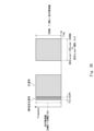
- FIG. 24 is a diagram showing a configuration example of the AAS 10 according to the present embodiment. Note that FIG. 24 shows only the main components of the AAS 10 according to this embodiment, and other components (for example, antennas, etc.) are not shown.
- the AAS 10 includes a signal processing unit 11, a TX 12 that is a transmitter, and a transmission AMP 13 that is a GaN AMP. Further, the signal processing section 11 includes a detection section 111, an IFFT (Inverse Fast Fourier Transform) section 112, a signal storage memory 113, and an adder 114.
- IFFT Inverse Fast Fourier Transform
- the IFFT unit 112 converts the DL signal from a frequency domain signal to a time domain signal.
- the detection section 111 is provided before the IFFT section 112.
- the detection unit 111 autonomously detects the presence or absence of a DL signal in the frequency domain. For example, the detection unit 111 detects the presence or absence of a DL signal by performing threshold determination in the frequency domain.
- the signal storage memory 113 stores an AMP stabilization signal for stabilizing the characteristics of the transmitting AMP 13. Specifically, when the AMP stabilization signal is input to the transmitting AMP 13, it quickly converges the current collapse and Gate/Drain Lag of the transmitting AMP 13, and quickly stabilizes the gain, output, and nonlinear distortion characteristics of the transmitting AMP 13. It is a signal that causes
- the adder 114 stores the DL signal in the signal storage memory 113 in a time domain before the time domain of the DL signal after the DL signal is output from the IFFT unit 112. Add the AMP stabilization signal. In this way, the AMP stabilization signal is inserted into the time domain before the time domain of the DL signal. At this time, the adder 114 calculates back the time at which the DL signal exists, taking into account the processing time of the TX 12 from the radiation time of the DL signal from the antenna, and inserts the AMP stabilization signal at the beginning of that time. .
- the AMP stabilization signal is inserted into the time domain before the time domain of the DL signal.
- the AMP stabilization signal can be passed through the TX 12 and the transmission AMP 13 before the DL signal passes through the TX 12 and the transmission AMP 13.
- the time domain before the time domain of the DL signal is, for example, the Tx On Transient period, which is a period for switching the TX 12 from Off to On. Therefore, the time width of the AMP stabilization signal is set within the time width of Tx On Transient period.
- Tx On Transient period is specified as 10 ⁇ sec in 3GPP NR.
- the frequency bandwidth of the AMP stabilization signal is set to the frequency bandwidth of the Component Carrier used for transmitting the DL signal.
- the power level of the AMP stabilization signal is set to a power level at which the output of the transmitting AMP 13 reaches the maximum rated RMS level, and is set to the same power level as the DL signal.
- the TX 12 is provided after the signal processing unit 11, and converts the DL signal or AMP stabilization signal output from the signal processing unit 11 from an IQ (In-Phase/Quadrature-Phase) signal to an RF signal. , output to the transmitting AMP 13.
- the TX 12 is provided in a TRX (not shown) that is a transmitter/receiver. Further, as described above, the TX 12 includes a DPP, a CFR provided before the DPD, etc., but illustration of these is omitted.
- the transmission AMP 13 is provided after the TX 12, and amplifies and outputs the DL signal or AMP stabilization signal output from the TX 12.
- the DL signal or AMP stabilization signal output from the transmission AMP 13 is transmitted to each UE via an antenna (not shown).
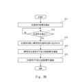
- FIG. 26 is a flowchart showing a schematic example of the operation of the AAS 10 according to the present embodiment.
- the detection unit 111 detects the presence or absence of a DL signal (step S11). If the detection unit 111 detects the DL signal (Yes in step S12), the adder 114 inserts the AMP stabilization signal into the time domain before the time domain of the DL signal (step S13). Therefore, first, the AMP stabilization signal passes through the TX 12 and the transmitting AMP 13 (step S14), thereby stabilizing the gain, output, and nonlinear distortion characteristics of the transmitting AMP 13. After that, the DL signal passes through the TX 12 and the transmission AMP 13 (step S15).
- the signal processing unit 11 when the signal processing unit 11 detects the DL signal, the signal processing unit 11 interrupts the AMP stabilization signal in the time domain before the time domain of the DL signal, so that the DL signal is connected to the TX 12 and Before passing through the transmission AMP 13, the AMP stabilization signal is passed through the TX 12 and the transmission AMP 13.
- the AM-AM/AM-PM characteristics of the transmitting AMP 13 in the first symbol section of the DL signal are already stable, so the first symbol of the DL signal and subsequent Symbols are stably compensated for distortion by the DPD within the TX 12. This also contributes to ensuring the signal quality of the DL signal from the first Symbol.
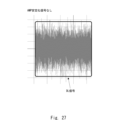
- FIG. 27 is a diagram showing an example of the amplitude waveform of a DL signal in an AAS equipped with a transmission AMP that is a GaN AMP with poor Gate/Drain Lag and no AMP stabilization signal provided.
- FIG. 28 shows the AMP stabilization signal and DL signal in the AAS 10 according to the present embodiment, which is equipped with a transmission AMP 13 that is a GaN AMP with poor Gate/Drain Lag and provides an AMP stabilization signal to the transmission AMP 13.
- FIG. 3 is a diagram showing an example of an amplitude waveform of FIG. In FIGS. 27 and 28, the horizontal axis shows time, and the vertical axis shows amplitude. The difference in amplitude waveforms in FIGS. 27 and 28 appears as a difference in EVM characteristics in FIGS. 29 and 30, which will be described later.
- FIG. 29 is a diagram showing an example of EVM characteristics when the transmitting AMP is turned on in an AAS equipped with a transmitting AMP that is a GaN AMP with poor Gate/Drain Lag and no AMP stabilization signal provided.
- FIG. 30 shows when the transmitting AMP 13 is turned on in the AAS 10 according to the present embodiment, which is equipped with the transmitting AMP 13 which is a GaN AMP with poor Gate/Drain Lag and gives an AMP stabilization signal to the transmitting AMP 13.
- FIG. 3 is a diagram showing an example of EVM characteristics.
- the horizontal axis represents Symbol
- the vertical axis represents EVM. Note that in FIGS. 29 and 30, the transmission AMP is turned on/off only once.
- FIG. 31 shows the DL signal immediately after turning on the transmitting AMP 13 in the AAS 10 according to the present embodiment, which is equipped with the transmitting AMP 13 which is a GaN AMP with poor Gate/Drain Lag and gives an AMP stabilization signal to the transmitting AMP 13.
- FIG. 3 is a diagram showing an example of a constellation of the first Symbol 1 of FIG.
- an example of the constellation of the first Symbol 1 of the DL signal immediately after turning on the transmitting AMP is shown in Figure 11. It is the same as the one above.
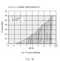
- FIG. 32 shows the SNR and FIG. 3 is a diagram showing an example of the relationship with throughput.
- the horizontal axis shows SNR and the vertical axis shows Throughput.
- an example of the relationship between SNR and Throughput for each of multiple MCSs in an AAS equipped with a transmitting AMP with poor Gate/Drain Lag and no AMP stabilization signal is shown in Figure 13. The same is true.
- the wireless communication device according to the present disclosure is used for AAS, but the present disclosure is not limited to this.
- the wireless communication device according to the present disclosure can be used in any wireless communication device (for example, a wide area base station, a macro base station, etc.) that has a transmission function to transmit a transmission signal.
- FIG. 33 is a diagram illustrating an example of the hardware configuration of the computer 20 that implements some of the functions of the wireless communication device according to the present disclosure. As shown in FIG. 33, the computer 20 includes a processor 21 and a memory 22.
- the processor 21 may be, for example, a microprocessor, a CPU, or an MPU (Micro Processing Unit). Processor 21 may include multiple processors.
- the memory 22 is configured by a combination of volatile memory and nonvolatile memory.
- Memory 22 may include storage located remotely from processor 21.
- the processor 21 may access the memory 22 via an I (Input)/O (Output) interface (not shown).
- a program is stored in the memory 22.
- This program includes a group of instructions (or software code) for causing the computer 20 to perform some of the functions of the AAS 10 according to the embodiment described above when loaded into the computer 20.
- the components of the AAS 10 described above may be realized by the processor 21 reading and executing a program stored in the memory 22. Further, the component having the storage function in the AAS 10 described above may be realized by the memory 22.
- the above-mentioned program may be stored in a non-transitory computer-readable medium or a tangible storage medium.
- computer readable or tangible storage media may include random-access memory (RAM), read-only memory (ROM), flash memory, solid-state drive (SSD) or other memory technology, CD - Including ROM, digital versatile disc (DVD), Blu-ray disc or other optical disc storage, magnetic cassette, magnetic tape, magnetic disc storage or other magnetic storage device.
- the program may be transmitted on a transitory computer-readable medium or a communication medium.
- transitory computer-readable or communication media includes electrical, optical, acoustic, or other forms of propagating signals.
Landscapes
- Engineering & Computer Science (AREA)
- Computer Networks & Wireless Communication (AREA)
- Signal Processing (AREA)
- Transmitters (AREA)
Abstract
Un système actif d'antenne (AAS) (10), selon la présente divulgation, comprend : une unité de traitement de signal (11) ; un émetteur (12) disposé en aval de l'unité de traitement de signal (11) ; et un amplificateur de transmission (13) disposé en aval de l'émetteur (12). L'unité de traitement de signal (11) détecte la présence/l'absence d'un signal de transmission, et si un signal de transmission a été détecté, un signal de stabilisation pour stabiliser les caractéristiques de l'amplificateur de transmission (13) est inséré dans le créneau temporel précédant le créneau temporel du signal de transmission, ce qui permet d'amener le signal de stabilisation à traverser l'émetteur (12) et l'amplificateur de transmission (13) avant que le signal de transmission ne traverse l'émetteur (12) et l'amplificateur de transmission (13).
Priority Applications (1)
| Application Number | Priority Date | Filing Date | Title |
|---|---|---|---|
| PCT/JP2022/016155 WO2023188161A1 (fr) | 2022-03-30 | 2022-03-30 | Dispositif de communication sans fil et procédé de communication sans fil |
Applications Claiming Priority (1)
| Application Number | Priority Date | Filing Date | Title |
|---|---|---|---|
| PCT/JP2022/016155 WO2023188161A1 (fr) | 2022-03-30 | 2022-03-30 | Dispositif de communication sans fil et procédé de communication sans fil |
Publications (1)
| Publication Number | Publication Date |
|---|---|
| WO2023188161A1 true WO2023188161A1 (fr) | 2023-10-05 |
Family
ID=88199714
Family Applications (1)
| Application Number | Title | Priority Date | Filing Date |
|---|---|---|---|
| PCT/JP2022/016155 WO2023188161A1 (fr) | 2022-03-30 | 2022-03-30 | Dispositif de communication sans fil et procédé de communication sans fil |
Country Status (1)
| Country | Link |
|---|---|
| WO (1) | WO2023188161A1 (fr) |
Citations (3)
| Publication number | Priority date | Publication date | Assignee | Title |
|---|---|---|---|---|
| JPH02116769A (ja) * | 1988-10-27 | 1990-05-01 | Tech Res & Dev Inst Of Japan Def Agency | パルス送信装置 |
| WO2012111274A1 (fr) * | 2011-02-14 | 2012-08-23 | パナソニック株式会社 | Amplificateur de puissance à haute fréquence |
| JP2021121054A (ja) * | 2020-01-30 | 2021-08-19 | 国立研究開発法人宇宙航空研究開発機構 | 増幅装置、送受信システム |
-
2022
- 2022-03-30 WO PCT/JP2022/016155 patent/WO2023188161A1/fr unknown
Patent Citations (3)
| Publication number | Priority date | Publication date | Assignee | Title |
|---|---|---|---|---|
| JPH02116769A (ja) * | 1988-10-27 | 1990-05-01 | Tech Res & Dev Inst Of Japan Def Agency | パルス送信装置 |
| WO2012111274A1 (fr) * | 2011-02-14 | 2012-08-23 | パナソニック株式会社 | Amplificateur de puissance à haute fréquence |
| JP2021121054A (ja) * | 2020-01-30 | 2021-08-19 | 国立研究開発法人宇宙航空研究開発機構 | 増幅装置、送受信システム |
Similar Documents
| Publication | Publication Date | Title |
|---|---|---|
| EP2909931B1 (fr) | Amplificateur réparti de suivi d'enveloppe | |
| US11973468B2 (en) | Apparatus and methods for envelope tracking | |
| US11881818B2 (en) | Envelope tracking for Doherty power amplifiers | |
| JP6567655B2 (ja) | 無線周波数(rf)電力増幅器回路とrf電力増幅器バイアス回路 | |
| TWI575866B (zh) | 校正在波封為基追蹤系統中之不變功率放大器負載特性的方法與裝置 | |
| CN102057568B (zh) | 用于ofdm/ofdma系统的agc和dc校准方法和系统 | |
| KR102059138B1 (ko) | 포락선 추적 보정 장치 및 방법 | |
| EP3130075B1 (fr) | Circuits et procédés de polarisation d'un amplificateur de puissance | |
| US10003310B1 (en) | Segmented digital predistortion apparatus and methods | |
| JPWO2010084544A1 (ja) | 高周波増幅器、無線装置及び制御方法 | |
| Saad et al. | The continuum of load modulation ratio from Doherty to traveling-wave amplifiers | |
| US20160227549A1 (en) | Radio device that has function to reduce peak power of multiplexed signal | |
| US11368175B2 (en) | Radio frequency control circuit | |
| EP3309959B1 (fr) | Système d'amplification et enodeb | |
| JP2007522746A (ja) | 減少した消費電力を有する無線送信機 | |
| WO2023188161A1 (fr) | Dispositif de communication sans fil et procédé de communication sans fil | |
| US20140010330A1 (en) | Transmission device and transmission method | |
| Nair et al. | A comparative study on digital predistortion techniques for Doherty amplifier for LTE applications | |
| Singh et al. | Design and performance analysis of broadband Doherty power amplifier for 5G communication system | |
| Shah et al. | Power-efficient LTE MACRO eNodeB: A comprehensive survey | |
| US20240089877A1 (en) | Wireless communication apparatus, wireless communication system, and wireless communication method | |
| Hussaini et al. | Optimum design of Doherty RFPA for mobile WiMAX base stations | |
| US20230126040A1 (en) | Power amplifier linearity control based on power amplifier operating mode or power level | |
| US20230396219A1 (en) | Signal amplification circuitry | |
| US20220360291A1 (en) | Efficient amplifer operation |
Legal Events
| Date | Code | Title | Description |
|---|---|---|---|
| 121 | Ep: the epo has been informed by wipo that ep was designated in this application |
Ref document number: 22935306 Country of ref document: EP Kind code of ref document: A1 |