WO2023182178A1 - 粗化処理銅箔、キャリア付銅箔、銅張積層板及びプリント配線板 - Google Patents
粗化処理銅箔、キャリア付銅箔、銅張積層板及びプリント配線板 Download PDFInfo
- Publication number
- WO2023182178A1 WO2023182178A1 PCT/JP2023/010440 JP2023010440W WO2023182178A1 WO 2023182178 A1 WO2023182178 A1 WO 2023182178A1 JP 2023010440 W JP2023010440 W JP 2023010440W WO 2023182178 A1 WO2023182178 A1 WO 2023182178A1
- Authority
- WO
- WIPO (PCT)
- Prior art keywords
- roughened
- copper foil
- filter
- resin
- particles
- Prior art date
- Legal status (The legal status is an assumption and is not a legal conclusion. Google has not performed a legal analysis and makes no representation as to the accuracy of the status listed.)
- Ceased
Links
Images



Classifications
-
- C—CHEMISTRY; METALLURGY
- C25—ELECTROLYTIC OR ELECTROPHORETIC PROCESSES; APPARATUS THEREFOR
- C25D—PROCESSES FOR THE ELECTROLYTIC OR ELECTROPHORETIC PRODUCTION OF COATINGS; ELECTROFORMING; APPARATUS THEREFOR
- C25D7/00—Electroplating characterised by the article coated
- C25D7/06—Wires; Strips; Foils
- C25D7/0614—Strips or foils
-
- C—CHEMISTRY; METALLURGY
- C25—ELECTROLYTIC OR ELECTROPHORETIC PROCESSES; APPARATUS THEREFOR
- C25D—PROCESSES FOR THE ELECTROLYTIC OR ELECTROPHORETIC PRODUCTION OF COATINGS; ELECTROFORMING; APPARATUS THEREFOR
- C25D1/00—Electroforming
- C25D1/04—Wires; Strips; Foils
-
- C—CHEMISTRY; METALLURGY
- C25—ELECTROLYTIC OR ELECTROPHORETIC PROCESSES; APPARATUS THEREFOR
- C25D—PROCESSES FOR THE ELECTROLYTIC OR ELECTROPHORETIC PRODUCTION OF COATINGS; ELECTROFORMING; APPARATUS THEREFOR
- C25D5/00—Electroplating characterised by the process; Pretreatment or after-treatment of workpieces
- C25D5/16—Electroplating with layers of varying thickness
-
- C—CHEMISTRY; METALLURGY
- C25—ELECTROLYTIC OR ELECTROPHORETIC PROCESSES; APPARATUS THEREFOR
- C25D—PROCESSES FOR THE ELECTROLYTIC OR ELECTROPHORETIC PRODUCTION OF COATINGS; ELECTROFORMING; APPARATUS THEREFOR
- C25D7/00—Electroplating characterised by the article coated
- C25D7/06—Wires; Strips; Foils
-
- H—ELECTRICITY
- H05—ELECTRIC TECHNIQUES NOT OTHERWISE PROVIDED FOR
- H05K—PRINTED CIRCUITS; CASINGS OR CONSTRUCTIONAL DETAILS OF ELECTRIC APPARATUS; MANUFACTURE OF ASSEMBLAGES OF ELECTRICAL COMPONENTS
- H05K1/00—Printed circuits
- H05K1/02—Details
- H05K1/09—Use of materials for the conductive, e.g. metallic pattern
Definitions
- the present invention relates to a roughened copper foil, a copper foil with a carrier, a copper-clad laminate, and a printed wiring board.
- thermoplastic resins with a low dielectric constant such as fluororesins and liquid crystal polymers (LCP) have low chemical activity and therefore have low adhesion to copper foil.
- the roughening particles have a ten-point average roughness Rzjis of 0.6 ⁇ m or more and 1.7 ⁇ m or less, and the half-width in the frequency distribution of the height of the roughening particles.
- a copper foil having a roughened surface having a roughness of 0.9 ⁇ m or less is disclosed. According to such a copper foil, it is possible to exhibit high peel strength even to an insulating resin base material, such as a liquid crystal polymer film, to which chemical adhesion cannot be expected.
- Patent Document 2 International Publication No. 2014/133164 discloses a copper foil having a particle size of 10 nm or more and 250 nm or less (for example, approximately spherical copper particles) attached to the copper foil to make it rough.
- a surface-treated copper foil is disclosed that has a black, roughened surface.
- Copper foils for high frequency applications are required to have finer roughening particles as described above, but such copper foils tend to have poor adhesion to resins (particularly thermoplastic resins).
- existing copper foils are not necessarily sufficient in terms of both high adhesion with thermoplastic resins and excellent high frequency properties, and there is room for improvement.
- the present inventors have recently discovered that by controlling the skewness Ssk and the peak density Sds within predetermined ranges on the surface of a roughened copper foil, the surface has high adhesion to thermoplastic resin and excellent high frequency properties. We found that it is possible to achieve both.
- an object of the present invention is to provide a roughened copper foil that is capable of achieving both high adhesion to a thermoplastic resin and excellent high frequency properties.
- a roughened copper foil having a roughened surface on at least one side has a skewness Ssk greater than 0.35 and a peak density Sds of 1.57 ⁇ m ⁇ 2 or more and 2.64 ⁇ m ⁇ 2 or less
- the Ssk is a value measured in accordance with JIS B0681-2:2018 without cutoff with an S filter and with a cutoff wavelength of 1.0 ⁇ m using an L filter
- the above-mentioned Sds is a value measured in accordance with EUR15178N without cutoff using an S filter and an L filter, and is a roughened copper foil.
- the roughened surface has a plurality of roughened particles, and the volume of the roughened particles per 1 ⁇ m 2 is 0.11 ⁇ m 3 or more and 0.25 ⁇ m 3 or less,
- Treated copper foil [Aspect 3]
- the roughened surface has a kurtosis Sku of 2.70 or more and 4.90 or less, The roughened copper foil according to aspect 1 or 2, wherein the Sku is a value measured in accordance with JIS B0681-2:2018 without cutoff by an S filter and an L filter.
- the roughened surface has a load area ratio Smr1 of 11.2% or more that separates the protruding peak portion and the core portion,
- the Smr1 is a value measured according to JIS B0681-2:2018 without cutoff with an S filter and with a cutoff wavelength of 1.0 ⁇ m using an L filter.
- the roughened copper foil described in .
- a copper-clad laminate comprising the roughened copper foil according to any one of aspects 1 to 5.
- a printed wiring board comprising the roughened copper foil according to any one of aspects 1 to 5.
- FIG. 3 is a diagram for explaining the skewness Ssk measured in accordance with JIS B0681-2:2018, and is a diagram showing the surface and its height distribution when Ssk ⁇ 0.
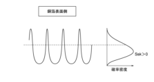
- FIG. 3 is a diagram for explaining the skewness Ssk measured in accordance with JIS B0681-2:2018, and is a diagram showing the surface and its height distribution when Ssk>0.
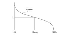
- FIG. 2 is a diagram for explaining a load curve and a load area ratio determined in accordance with JIS B0681-2:2018.
- FIG. 3 is a diagram for explaining the load area ratio Smr1 that separates the protruding peak portion and the core portion, which is measured in accordance with JIS B0681-2:2018. This is a resin replica image after binarization obtained in Example 3.
- FIG. 3 is a diagram for explaining the load area ratio Smr1 that separates the protruding peak portion and the core portion, which is measured in accordance with JIS B0681-2:2018.
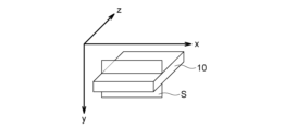
- FIG. 4 is a diagram showing the x-axis, y-axis, z-axis, and slice plane S in FIB-SEM observation and three-dimensional image analysis in relation to the roughened copper foil. It is a slice image of the roughened copper foil of Example 9 after forming markings and a protective film. This is an image for explaining material assignment in three-dimensional image analysis. This is the first inference image generated by machine learning the image in FIG. This is an example of a slice image in which the roughened bottom surface of the roughened copper foil and the roughened particles are continuous. This is an example of a slice image in which the roughened bottom surface of the roughened copper foil and the roughened particles are discontinuous.
- skewness Ssk or “Ssk” is a parameter representing the symmetry of height distribution, measured in accordance with JIS B0681-2:2018.
- this value indicates that the height distribution is vertically symmetrical, in other words, it indicates that bumps (roughening particles, etc.) of uniform size are arranged on the surface.
- FIG. 1A if this value is smaller than 0, it indicates that the surface has many small valleys, or in other words, that thick rounded bumps are lined up on the surface.
- FIG. 1B if this value is greater than 0, it indicates that the surface has many fine mountains, or in other words, that the surface is dotted with elongated bumps.
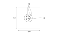
- mountain peak density Sds or “Sds” is a parameter representing the number of peaks per unit area, measured in accordance with EUR15178N.
- Sds a point higher than the eight neighboring points N is regarded as the mountaintop S. The larger this value is, the denser the bumps are (see FIG. 2A). On the other hand, the smaller this value is, the more sparsely the bumps are present (see FIG. 2B).
- surface load curve refers to the height at which the load area ratio is from 0% to 100%, determined in accordance with JIS B0681-2:2018.
- the load area ratio at height c corresponds to Smr(c) in FIG.
- the secant line of the load curve drawn from the load area ratio of 0% along the load curve with the difference in the load area ratio of 40% is moved from the load area ratio of 0%, and the secant line The position where the slope of is the gentlest is called the center of the surface load curve.
- the straight line that minimizes the sum of squares of deviations in the vertical axis direction with respect to this central part is called an equivalent straight line.
- the portion included in the height range of 0% to 100% of the load area ratio of the equivalent straight line is called the core portion.
- the portion higher than the core portion is called a protruding peak portion, and the portion lower than the core portion is called a protruding trough portion.
- load area ratio Smr1 that separates the protruding mountain part and the core part refers to the core part measured in accordance with JIS B0681-2:2018, as shown in FIG. This is a parameter that represents the load area ratio at the intersection of the upper height of the surface and the surface load curve (i.e., the load area ratio that separates the core portion from the protruding peak portion).
- Sku is a parameter representing the sharpness of the height distribution, which is measured in accordance with JIS B0681-2:2018, and is also referred to as kurtosis.
- Sku>3 there are many sharp peaks and valleys on the surface, in other words, there are many fine bumps standing on the surface.
- Sku ⁇ 3 means that the surface is flat, in other words, thick rounded bumps are arranged on the surface.
- Ssk, Sds, Smr1 and Sku can be calculated by measuring the surface profile of a predetermined measurement area (for example, a two-dimensional area of 64.397 ⁇ m x 64.463 ⁇ m) on the roughened surface using a commercially available laser microscope. can.
- a predetermined measurement area for example, a two-dimensional area of 64.397 ⁇ m x 64.463 ⁇ m
- Ssk and Smr1 are measured under conditions of a cutoff wavelength of 1.0 ⁇ m using an L filter and no cutoff using an S filter.
- Sds and Sku are measured under conditions where no cutoff is performed using the S filter and the L filter.
- Other preferable measurement conditions and analysis conditions for the surface profile using a laser microscope will be shown in Examples below.
- volume of roughened particles per 1 ⁇ m 2 is a value calculated by three-dimensional analysis of an image obtained using FIB-SEM of a roughened surface.
- This three-dimensional analysis can be preferably performed by the following procedure using commercially available three-dimensional image processing software (for example, Dragonfly (version 2022.1.0.1259) manufactured by Object Research System).
- (1) Read the slice image of the roughened copper foil obtained by FIB-SEM and perform alignment.
- (2) Perform trimming of the slice image.
- Machine learning is performed to extract the Cu portion originating from the roughened copper foil, and a segmentation model is created.
- Apply the segmentation model to the slice image and extract the Cu portion.
- Trim a predetermined analysis area for example, 4.5 ⁇ m x 4.5 ⁇ m
- the "electrode surface" of the electrolytic copper foil refers to the surface that was in contact with the cathode during manufacture of the electrolytic copper foil.
- the "deposition surface" of an electrolytic copper foil refers to the surface on which electrolytic copper is deposited during production of the electrolytic copper foil, that is, the surface that is not in contact with the cathode.
- the copper foil according to the present invention is a roughened copper foil.
- This roughened copper foil has a roughened surface on at least one side.
- This roughened surface has a skewness Ssk greater than 0.35.
- this roughened surface has a peak density Sds of 1.57 ⁇ m ⁇ 2 or more and 2.64 ⁇ m ⁇ 2 or less.
- thermoplastic resins with a low dielectric constant such as fluororesins and liquid crystal polymers (LCP) have low chemical activity and therefore have low adhesion to copper foil, unlike thermosetting resins.
- copper foil with low roughness which is advantageous in terms of high frequency characteristics, tends to inherently have poor adhesion to resin.
- the roughened copper foil of the present invention it is possible to unexpectedly achieve both high adhesion with the thermoplastic resin and excellent high frequency characteristics (for example, reduction of skin effect).
- the skin effect can be reduced compared to roughening particles that are thick and large in shape (Ssk ⁇ 0).
- the roughened surface with a peak density Sds of 1.57 ⁇ m ⁇ 2 or more and 2.64 ⁇ m ⁇ 2 or less has a moderate density of bumps, and has high adhesion with thermoplastic resin and excellent high frequency characteristics. It can be achieved in a well-balanced manner. That is, the peak density Sds is a parameter representing the number of peaks per unit area as described above, and in other words, it can be said to be a parameter related to the size of the roughened particles on the roughened surface.
- the size of the roughened particles becomes fine, resulting in a surface shape that is effective in reducing the skin effect.
- the peak density Sds of the roughened surface is 2.64 ⁇ m -2 or less, the size of the roughened particles becomes appropriate, and the surface can exhibit a high anchoring effect with the thermoplastic resin base material. It becomes a shape. As a result, it is thought that it becomes possible to achieve both high adhesion with the thermoplastic resin and excellent high frequency properties.
- the Ssk of the roughened surface is greater than 0.35, preferably greater than 0.35 and less than or equal to 0.79, and more preferably greater than or equal to 0.36 and less than or equal to 0.57.
- the roughened copper foil has an Sds of 1.57 ⁇ m ⁇ 2 or more and 2.64 ⁇ m ⁇ 2 or less, preferably 1.57 ⁇ m ⁇ 2 or more and 2.57 ⁇ m ⁇ 2 or less, and more preferably 1. .62 ⁇ m -2 or more and 2.57 ⁇ m -2 or less.
- the roughened copper foil has a plurality of roughened particles on the roughened surface.
- the volume of the roughened particles per 1 ⁇ m 2 of the roughened surface is preferably 0.11 ⁇ m 3 or more and 0.25 ⁇ m 3 or less, more preferably 0.11 ⁇ m 3 or more and 0.18 ⁇ m 3 or less, and even more preferably 0.11 ⁇ m 3 or more and 0.16 ⁇ m 3 or less.
- the surface shape will have fine roughened particles that are effective in reducing the skin effect, and while ensuring high adhesion with the thermoplastic resin, Even better high frequency characteristics can be achieved.
- the roughened copper foil preferably has a Sku of 2.70 or more and 4.90 or less, more preferably 3.00 or more and 4.00 or less, and even more preferably 3.00 or more and 3.60. It is as follows. When Sku is within the above range, high adhesion to the thermoplastic resin and excellent high frequency properties can be achieved in a better balance.
- the roughened copper foil preferably has an Smr1 of 11.2% or more on the roughened surface, more preferably 11.2% or more and 13.4% or less, and even more preferably 11.3% or more and 12.4%. % or less.
- Smr1 is within the above range, high adhesion to the thermoplastic resin and excellent high frequency properties can be achieved in a better balance.
- the thickness of the roughened copper foil is not particularly limited, but is preferably 0.1 ⁇ m or more and 35 ⁇ m or less, more preferably 0.5 ⁇ m or more and 5.0 ⁇ m or less, and even more preferably 1.0 ⁇ m or more and 3.0 ⁇ m or less.
- the roughened copper foil is not limited to one in which the surface of a normal copper foil is roughened, but may be one in which the surface of a copper foil with a carrier is roughened.
- the thickness of the roughened copper foil is the thickness that does not include the height of the roughening particles formed on the surface of the roughened surface (the thickness of the copper foil itself that constitutes the roughened copper foil) It is.
- the roughened copper foil has a roughened surface on at least one side. That is, the roughened copper foil may have a roughened surface on both sides, or may have a roughened surface only on one side. As described above, the roughened surface preferably includes a plurality of roughened particles (preferably vertically elongated roughened particles), and each of these plurality of roughened particles is more preferably made of copper particles.
- the copper particles may be made of metallic copper or may be made of a copper alloy.
- the roughening treatment for forming the roughened surface can be preferably performed by forming roughening particles of copper or copper alloy on the copper foil.
- This roughening treatment is preferably performed according to a plating method that involves a two-step plating process.
- the copper concentration is 5 g/L or more and 9 g/L or less (more preferably 7 g/L or more and 9 g/L or less)
- the sulfuric acid concentration is 100 g/L or more and 150 g/L or less (more preferably 100 g/L or more and 150 g/L or less).
- Electrodeposition is preferably performed using a copper sulfate solution with a tungsten concentration of 5 mg/L or more and 20 mg/L or less (more preferably 10 mg/L or more and 20 mg/L or less). This electrodeposition is carried out at a liquid temperature of 20°C or more and 50°C or less (more preferably 30°C or more and 50°C or less) and a current density of 10 A/ dm2 or more and 40 A/dm2 or less (more preferably 20 A/ dm2 or more and 40 A/dm2 or less) . (below) and an electrical quantity of 50 A ⁇ s to 200 A ⁇ s (more preferably 50 A ⁇ s to 150 A ⁇ s).
- the copper concentration is 40 g/L or more and 70 g/L or less (more preferably 50 g/L or more and 70 g/L or less), and the sulfuric acid concentration is 100 g/L or more and 300 g/L or less (more preferably 150 g/L).
- Electrodeposition is preferably performed using a copper sulfate solution (250 g/L or less).
- This electrodeposition is performed at a liquid temperature of 30°C or more and 60°C or less (more preferably 40°C or more and 50°C or less) and a current density of 10 A/ dm2 or more and 40 A/dm2 or less (more preferably 20 A/dm2 or more and 40 A/dm2 or less) .
- the plating conditions are preferably 10 A ⁇ s or more and 250 A ⁇ s or less (more preferably 10 A ⁇ s or more and 150 A ⁇ s or less).
- the roughened copper foil may be subjected to rust prevention treatment and may have a rust prevention treatment layer formed thereon.
- the rust prevention treatment includes plating treatment using zinc.
- the plating treatment using zinc may be either a zinc plating treatment or a zinc alloy plating treatment, and the zinc alloy plating treatment is particularly preferably a zinc-nickel alloy treatment.
- the zinc-nickel alloy treatment may be a plating treatment that contains at least Ni and Zn, and may further contain other elements such as Sn, Cr, and Co.
- the Ni/Zn adhesion ratio in zinc-nickel alloy plating is preferably 1.2 or more and 10 or less, more preferably 2 or more and 7 or less, and even more preferably 2.7 or more and 4 or less, in terms of mass ratio.
- the rust prevention treatment further includes chromate treatment, and it is more preferable that this chromate treatment is performed on the surface of the plating containing zinc after the plating treatment using zinc.
- a particularly preferred anticorrosion treatment is a combination of zinc-nickel alloy plating treatment followed by chromate treatment.
- the surface of the roughened copper foil may be treated with a silane coupling agent to form a silane coupling agent layer.
- a silane coupling agent layer can be formed by appropriately diluting a silane coupling agent, applying it, and drying it.
- silane coupling agents include epoxy-functional silane coupling agents such as 4-glycidylbutyltrimethoxysilane, 3-glycidoxypropyltrimethoxysilane, or 3-aminopropyltrimethoxysilane, N-(2- aminoethyl)-3-aminopropyltrimethoxysilane, N-3-(4-(3-aminopropoxy)butoxy)propyl-3-aminopropyltrimethoxysilane, N-phenyl-3-aminopropyltrimethoxysilane, etc.
- epoxy-functional silane coupling agents such as 4-glycidylbutyltrimethoxysilane, 3-glycidoxypropyltrimethoxysilane, or 3-aminopropyltrimethoxysilane, N-(2- aminoethyl)-3-aminopropyltrimethoxysilane, N-3-(4-(3-aminopropoxy)but
- Amino-functional silane coupling agents or mercapto-functional silane coupling agents such as 3-mercaptopropyltrimethoxysilane, or olefin-functional silane coupling agents such as vinyltrimethoxysilane, vinylphenyltrimethoxysilane, or 3-methacrylic Examples include acrylic-functional silane coupling agents such as roxypropyltrimethoxysilane, or imidazole-functional silane coupling agents such as imidazole silane, or triazine-functional silane coupling agents such as triazine silane.
- the roughened copper foil further includes a rust prevention treatment layer and/or a silane coupling agent layer on the roughening treatment surface, and more preferably, a rust prevention treatment layer and/or a silane coupling agent layer.
- a rust prevention treatment layer and/or a silane coupling agent layer are formed on the roughening treatment surface, the numerical values of various parameters of the roughening treatment surface in this specification are based on the rust prevention treatment layer and/or the silane coupling agent layer. It means the numerical value obtained by measuring and analyzing the roughened copper foil after the treatment layer has been formed.
- the rust prevention layer and the silane coupling agent layer may be formed not only on the roughened surface side of the roughened copper foil but also on the side where the roughened surface is not formed.
- the roughened copper foil of the present invention may be provided in the form of a copper foil with a carrier. That is, according to a preferred embodiment of the present invention, the method includes a carrier, a release layer provided on the carrier, and the roughened copper foil provided on the release layer with the roughened surface facing outward. A copper foil with a carrier is provided.
- the carrier-attached copper foil may have any known layer structure, except for using the roughened copper foil of the present invention.
- the carrier is a support for supporting the roughened copper foil to improve its handling properties, and a typical carrier includes a metal layer.
- a typical carrier includes a metal layer.
- Examples of such carriers include aluminum foil, copper foil, stainless steel (SUS) foil, resin films whose surfaces are metal-coated with copper or the like, glass, and the like, with copper foil being preferred.
- the copper foil may be either a rolled copper foil or an electrolytic copper foil, but preferably an electrolytic copper foil.
- the thickness of the carrier is typically 250 ⁇ m or less, preferably 9 ⁇ m or more and 200 ⁇ m or less.
- the peeling layer is a layer that has the function of weakening the peeling strength of the carrier, ensuring the stability of this strength, and further suppressing mutual diffusion that may occur between the carrier and the copper foil during press molding at high temperatures.
- the release layer may be either an organic release layer or an inorganic release layer.
- organic components used in the organic release layer include nitrogen-containing organic compounds, sulfur-containing organic compounds, carboxylic acids, and the like.
- nitrogen-containing organic compound include triazole compounds, imidazole compounds, etc. Among them, triazole compounds are preferred because they have easy releasability.
- triazole compounds examples include 1,2,3-benzotriazole, carboxybenzotriazole, N',N'-bis(benzotriazolylmethyl)urea, 1H-1,2,4-triazole and 3-amino- Examples include 1H-1,2,4-triazole.
- sulfur-containing organic compounds examples include mercaptobenzothiazole, thiocyanuric acid, 2-benzimidazolethiol, and the like.
- carboxylic acids include monocarboxylic acids, dicarboxylic acids, and the like.
- examples of inorganic components used in the inorganic release layer include Ni, Mo, Co, Cr, Fe, Ti, W, P, Zn, and a chromate-treated film.
- the release layer may be formed by, for example, bringing a release layer component-containing solution into contact with at least one surface of the carrier to fix the release layer component on the surface of the carrier.
- this contact may be carried out by dipping the carrier in the release layer component-containing solution, spraying the release layer component-containing solution, flowing down the release layer component-containing solution, or the like.
- a method of forming a film with the release layer component by a vapor phase method such as vapor deposition or sputtering.
- the release layer component may be fixed to the carrier surface by adsorption or drying of a solution containing the release layer component, or by electrodeposition of the release layer component in the solution containing the release layer component.
- the thickness of the release layer is typically 1 nm or more and 1 ⁇ m or less, preferably 5 nm or more and 500 nm or less.
- auxiliary metal layers may be provided between the release layer and the carrier and/or the roughened copper foil.
- other functional layers include auxiliary metal layers.
- the auxiliary metal layer consists of nickel and/or cobalt.
- the thickness of the auxiliary metal layer is preferably 0.001 ⁇ m or more and 3 ⁇ m or less.
- the roughened copper foil of the present invention is preferably used for producing a copper-clad laminate for printed wiring boards. That is, according to a preferred embodiment of the present invention, a copper-clad laminate including the roughened copper foil is provided.
- This copper-clad laminate includes the roughened copper foil of the present invention and a resin layer provided in close contact with the roughened surface of the roughened copper foil.
- the roughened copper foil may be provided on one side or both sides of the resin layer.
- the resin layer contains a resin, preferably an insulating resin.
- the resin layer is a prepreg and/or a resin sheet.
- Prepreg is a general term for composite materials in which a base material such as a synthetic resin plate, glass plate, glass woven fabric, glass nonwoven fabric, or paper is impregnated with synthetic resin.
- the resin layer may contain filler particles made of various inorganic particles such as silica and alumina from the viewpoint of improving insulation properties.
- the thickness of the resin layer is not particularly limited, but is preferably 1 ⁇ m or more and 1000 ⁇ m or less, more preferably 2 ⁇ m or more and 400 ⁇ m or less, and even more preferably 3 ⁇ m or more and 200 ⁇ m or less.
- the resin layer may be composed of multiple layers.
- a resin layer such as a prepreg and/or a resin sheet may be provided on the roughened copper foil via a primer resin layer that is previously applied to the surface of the copper foil.
- the resin layer preferably contains a thermoplastic resin, and more preferably most (for example, 50% by weight or more) or most ( For example, 80% by weight or more or 90% by weight or more) is thermoplastic resin.
- thermoplastic resins include polysulfone (PSF), polyethersulfone (PES), amorphous polyarylate (PAR), liquid crystal polymer (LCP), polyetheretherketone (PEEK), and thermoplastic polyimide (PI).
- thermoplastic resins include polysulfone (PSF), polyethersulfone (PES), amorphous polyarylate (PAR), liquid crystal polymer (LCP), and polysulfone.
- thermoplastic resins include liquid crystal polymers (LCP) and/or fluororesins.
- fluororesin include polytetrafluoroethylene (PTFE), tetrafluoroethylene/perfluoroalkyl vinyl ether copolymer (PFA), tetrafluoroethylene/hexafluoropropylene copolymer (FEP), and tetrafluoroethylene-ethylene. copolymers (ETFE), and any combination thereof.
- the insulating resin base material it is preferable to attach to the roughened copper foil by pressing while heating. This softens the thermoplastic resin and allows it to penetrate into the fine irregularities of the roughened surface. can be set. As a result, the adhesion between the copper foil and the resin can be ensured due to the anchor effect caused by the fine irregularities (particularly the vertically elongated roughened particles) biting into the resin.
- the roughened copper foil of the present invention is preferably used for producing printed wiring boards. That is, according to a preferred embodiment of the present invention, a printed wiring board including the roughened copper foil is provided. By using the roughened copper foil of the present invention, it is possible to achieve both excellent high frequency characteristics and high circuit adhesion in the manufacture of printed wiring boards.
- the printed wiring board according to this embodiment includes a layered structure in which a resin layer and a copper layer are laminated.
- the copper layer is a layer derived from the roughened copper foil of the present invention. Further, the resin layer is as described above regarding the copper-clad laminate.
- the printed wiring board may have a known layer structure, except for using the roughened copper foil of the present invention.
- printed wiring boards include single-sided or double-sided printed wiring boards in which the roughened copper foil of the present invention is adhered to one or both sides of prepreg to form a cured laminate, and circuits are formed on the cured laminate, and multilayered versions of these. Examples include multilayer printed wiring boards. Further, other specific examples include flexible printed wiring boards, COF, TAB tapes, etc. in which a circuit is formed by forming the roughened copper foil of the present invention on a resin film. As another specific example, a resin-coated copper foil (RCC) is formed by applying the above-mentioned resin layer to the roughened copper foil of the present invention, and the resin layer is laminated on the above-mentioned printed circuit board as an insulating adhesive layer.
- RRCC resin-coated copper foil
- build-up wiring boards in which circuits are formed using methods such as modified semi-additive method (MSAP) or subtractive method using the roughened copper foil as all or part of the wiring layer, and the roughened copper foil are removed.
- MSAP modified semi-additive method
- Examples include a build-up wiring board in which a circuit is formed using a semi-additive method (SAP), and a direct build-up on wafer in which lamination of resin-coated copper foil and circuit formation are alternately repeated on a semiconductor integrated circuit.
- More advanced examples include antenna elements in which the resin-coated copper foil is laminated onto a base material to form a circuit, electronic materials for panels and displays, and windows in which patterns are formed by laminating the resin-coated copper foil onto glass or resin film via an adhesive layer.
- Examples include electronic materials for glass, electromagnetic shielding films made by applying a conductive adhesive to the roughened copper foil of the present invention, and the like.
- printed wiring boards equipped with the roughened copper foil of the present invention can be used in applications such as automotive antennas, mobile phone base station antennas, high-performance servers, and collision prevention radars used in high frequency bands of signal frequencies of 10 GHz or higher. It is suitably used as a high frequency substrate.
- Examples 1 to 11 The roughened copper foil of the present invention was manufactured as follows.
- the conditions for the roughening treatment at each stage were as follows. - In the first roughening treatment, sulfuric acid, copper sulfate, and optionally sodium tungstate as an inorganic additive (Examples 1 to 6, 8, and 9 Electroplating was carried out using an acidic copper sulfate solution containing ) under the electrodeposition conditions (liquid temperature, current density, and quantity of electricity) shown in Table 1. - In the second roughening treatment, an acidic copper sulfate solution containing sulfuric acid and copper sulfate was used under the electrodeposition conditions (liquid temperature, current Electroplating was carried out at the following density and electrical charge).
- the roughened surface of the electrolytic copper foil was subjected to rust prevention treatment consisting of zinc-nickel alloy plating treatment and chromate treatment.
- a zinc-nickel alloy plating treatment was performed using a solution containing a zinc concentration of 1 g/L, a nickel concentration of 2 g/L, and a potassium pyrophosphate concentration of 80 g/L under conditions of a liquid temperature of 40°C and a current density of 0.5 A/ dm2 . I did it.
- the surface subjected to the zinc-nickel alloy plating treatment was subjected to chromate treatment using an aqueous solution containing 1 g/L of chromic acid under conditions of pH 12 and current density of 1 A/dm 2 .
- Silane coupling agent treatment An aqueous solution of 3-aminopropyltrimethoxysilane with a concentration of 6 g/L is adsorbed on the roughened surface of the electrolytic copper foil, and the water is evaporated with an electric heater to form a silane cup. Ring agent treatment was performed. At this time, the silane coupling agent treatment was not performed on the surface of the electrolytic copper foil that had not been subjected to the roughening treatment.
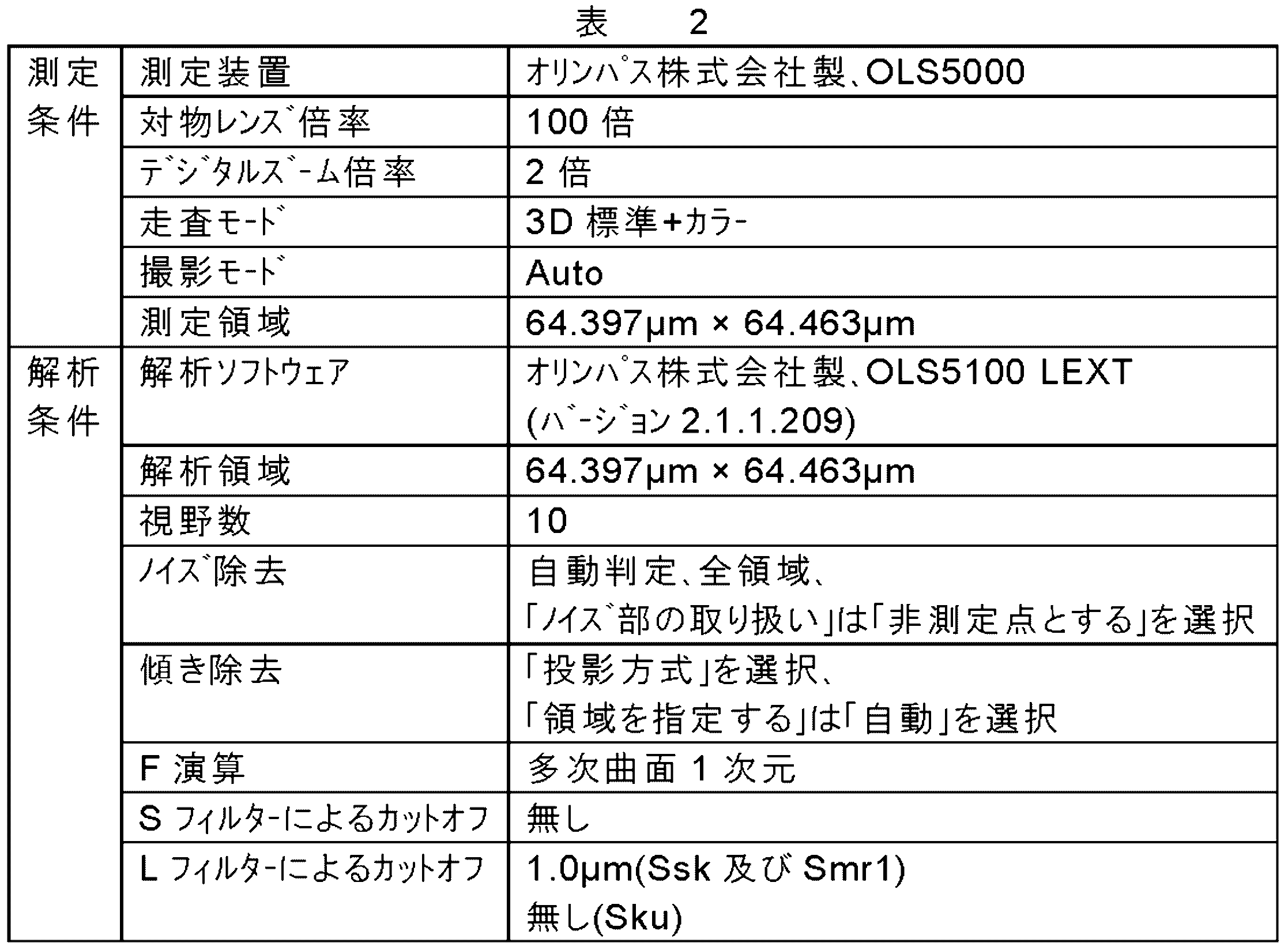
- the roughened surface of the roughened copper foil was measured by surface roughness analysis using a laser microscope in accordance with JIS B0681-2:2018 (Ssk, Sku and Smr1) or EUR15178N (Sds).
- the specific measurement conditions were as shown in Table 2.
- the surface profile of the obtained roughened surface was analyzed according to the conditions shown in Table 2, and Ssk, Sku, and Smr1 were calculated.
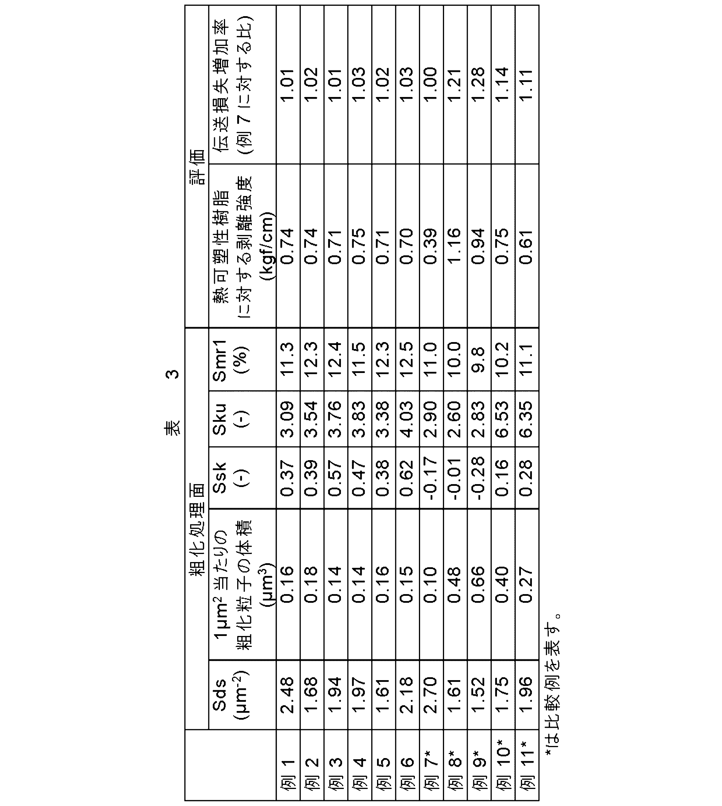
- the above parameters were calculated in 10 different visual fields, and the average value in all the visual fields was adopted as the surface texture parameter of the roughened surface of the sample. The results were as shown in Table 3.
- Sds was calculated as follows. First, the measurement data obtained with the laser microscope described above is loaded into the analysis software (Olympus Corporation, "OLS5100 LEXT (version 2.1.2.215)”), and the unprocessed data is converted to the LEXT file format. Output was performed. This LEXT file was read and analyzed using another analysis software (Digital Surf, "MountainsMap (version 9.0.9878)”) (analysis area: 64.397 ⁇ m x 64.463 ⁇ m). Specifically, the "parameter table” and “default settings” were selected in this order from the analysis target tab to display the parameter analysis screen.
- Root diameter of roughening particles The root diameter of the roughening particles used in the three-dimensional analysis of slice images to be described later was calculated as follows. First, prepreg (manufactured by Panasonic Corporation, R-5670NF, 45 ⁇ m thick x 2 sheets) was prepared as a resin film. The obtained roughened copper foils were laminated so that their roughened surfaces were in contact with the resin film, and using a vacuum press machine, they were pressed at a pressure of 3.0 MPa, a temperature of 190°C, and a pressing time of 90 minutes. Pressing was performed to produce a copper-clad laminate. The roughened copper foil was removed from this copper-clad laminate using a cupric chloride etching solution.
- resin replica a resin film having a surface onto which the surface shape of the roughened surface was transferred was obtained.
- resin replica a resin film having a surface onto which the surface shape of the roughened surface was transferred was obtained.
- FE-SEM Schottky field emission scanning electron microscope
- Image analysis was performed on the obtained resin replica image using image analysis software (manufactured by Nireco Co., Ltd., "LUZEX (version 1.60.8.2)") as follows.
- a binarization process was performed on the resin replica image under the condition of a threshold value of 125.
- the resin replica image after binarization obtained in Example 3 is shown in FIG.
- the area displayed in black was regarded as the root portion R of the transferred roughening particles.
- Slice images were acquired under the following measurement conditions using a FIB-SEM device (Carl Zeiss, Crossbeam 540, SEM and FIB simultaneous control: Atlas Engine v5.5.3).
- FIG. 7 shows an example of a slice image of the roughened copper foil of Example 9 in which the treatment was performed.
- a thermosetting resin 14 epoxy (G-2), manufactured by Gatan, Inc.) was applied to the roughened surface of the roughened copper foil 10 so that the roughened particles 12 were completely buried ( Coating thickness: 2.0 ⁇ m or more and 4.5 ⁇ m or less).
- the thermosetting resin 14 was cured by heating the roughened copper foil 10 coated with the resin at 120° C.
- the roughened copper foil 10 after cooling is put into the above-mentioned FIB-SEM device, and using the deposition function of the FIB, a platinum film 16 (thickness 1 .0 ⁇ m or more and 1.5 ⁇ m or less). Then, using the etching function of the FIB, the surface (xz plane) of the platinum film 16 is etched in the z-axis direction so that the same markings (three wedge shapes) can be visually recognized in each slice image. Processing was performed along the line to form a marking M. At this time, the machining depth in the y-axis direction was set to two-thirds or less of the thickness of the formed platinum film 16.
- a carbon film 18 (about 1 ⁇ m thick) was formed on the surface of the platinum film 16 using the FIB deposition function.
- the platinum film 16 and the carbon film 18 will be collectively referred to as the "protective film 20.”
- ROI means "a partial region of interest in an image” to which filter processing or recognition processing is applied. If there are cavities (uncolored areas) in “Cu”, the roughening particles 12 cannot be extracted accurately, so select the generated “ROI” and select “Fill inner areas: 3D” in “ROI tools”. ” and clicked “Apply” to perform the process of filling the cavity.
- thermoplastic resin liquid crystal polymer
- LCP liquid crystal polymer
- the obtained roughened copper foil was laminated on this thermoplastic resin base material so that its roughened surface was in contact with the resin base material, and using a vacuum press machine, press pressure was 4 MPa, temperature was 330°C, Pressing was performed under conditions of a pressing time of 10 minutes to produce a copper-clad laminate.
- a circuit was formed on this copper-clad laminate by a subtractive method using a cupric chloride etching solution to produce a test board having a linear circuit with a width of 3 mm.
- the formed test board was tested using a tabletop precision universal testing machine (AGS-50NX, manufactured by Shimadzu Corporation) in accordance with JIS C 5016-1994 method A (90° peeling).
- the film was peeled off from the thermoplastic resin base material to measure normal peel strength (kgf/cm). When this peel strength was 0.60 kgf/cm or more, it was determined to be acceptable.
- the results were as shown in Table 3.
- High-frequency base materials (MEGTRON6N, manufactured by Panasonic Corporation, 45 ⁇ m thick x 2 sheets) were prepared as insulating resin base materials.
- the obtained roughened copper foil was laminated on both sides of this insulating resin base material so that the roughened surface was in contact with the insulating resin base material, and a vacuum press was used to press the foil at a pressure of 3 MPa and a temperature of 190°C. Pressing was performed under the conditions of 90 minutes of pressing time to obtain a copper-clad laminate.
- circuit height 18 ⁇ m, circuit width: 300 ⁇ m, circuit length: 300 mm
- circuit length 300 mm
- a substrate for transmission loss measurement was obtained in which a microstrip line was formed so that the characteristic impedance was 50 ⁇ 2 ⁇ .
- the obtained transmission loss measurement board was measured using a network analyzer (manufactured by Keysight Technologies, N5225B) under the following setting conditions, and the transmission loss L 1 (dB) at 50 GHz was measured.
Landscapes
- Chemical & Material Sciences (AREA)
- Engineering & Computer Science (AREA)
- Chemical Kinetics & Catalysis (AREA)
- Electrochemistry (AREA)
- Materials Engineering (AREA)
- Metallurgy (AREA)
- Organic Chemistry (AREA)
- Microelectronics & Electronic Packaging (AREA)
- Laminated Bodies (AREA)
Abstract
Description
[態様1]
少なくとも一方の側に粗化処理面を有する粗化処理銅箔であって、
前記粗化処理面は、スキューネスSskが0.35より大きく、かつ、山頂密度Sdsが1.57μm-2以上2.64μm-2以下であり、
前記Sskは、JIS B0681-2:2018に準拠してSフィルターによるカットオフを行わず、Lフィルターによるカットオフ波長1.0μmの条件で測定される値であり、
前記Sdsは、EUR15178Nに準拠してSフィルター及びLフィルターによるカットオフを行わない条件で測定される値である、粗化処理銅箔。
[態様2]
前記粗化処理面は、複数の粗化粒子を有しており、1μm2当たりの前記粗化粒子の体積が0.11μm3以上0.25μm3以下であり、
前記1μm2当たりの粗化粒子の体積は、前記粗化処理面に対してFIB-SEMを用いて得られる画像を三次元解析することにより算出される値である、態様1に記載の粗化処理銅箔。
[態様3]
前記粗化処理面は、クルトシスSkuが2.70以上4.90以下であり、
前記Skuは、JIS B0681-2:2018に準拠してSフィルター及びLフィルターによるカットオフを行わない条件で測定される値である、態様1又は2に記載の粗化処理銅箔。
[態様4]
前記粗化処理面は、突出山部とコア部を分離する負荷面積率Smr1が11.2%以上であり、
前記Smr1は、JIS B0681-2:2018に準拠してSフィルターによるカットオフを行わず、Lフィルターによるカットオフ波長1.0μmの条件で測定される値である、態様1~3のいずれか一つに記載の粗化処理銅箔。
[態様5]
前記粗化処理面に防錆処理層及び/又はシランカップリング剤層をさらに備えた、態様1~4のいずれか一つに記載の粗化処理銅箔。
[態様6]
キャリアと、該キャリア上に設けられた剥離層と、該剥離層上に前記粗化処理面を外側にして設けられた態様1~5のいずれか一つに記載の粗化処理銅箔とを備えた、キャリア付銅箔。
[態様7]
態様1~5のいずれか一つに記載の粗化処理銅箔を備えた、銅張積層板。
[態様8]
態様1~5のいずれか一つに記載の粗化処理銅箔を備えた、プリント配線板。
本発明を特定するために用いられる用語ないしパラメータの定義を以下に示す。
(1)FIB-SEMにより取得した粗化処理銅箔のスライス画像を読み込み、位置合わせを行う。
(2)スライス画像のトリミングを実施する。
(3)粗化処理銅箔に由来するCu部分を抽出するための機械学習を行い、セグメンテーションモデルを作成する。
(4)セグメンテーションモデルをスライス画像に適用し、Cu部分の抽出を行う。
(5)粗化粒子の根元径に基づき、Cu部分から粗化粒子の抽出を行う。
(6)所定の解析領域(例えば4.5μm×4.5μm)のトリミングを行い、1μm2当たりの粗化粒子の体積を算出する。
本発明による銅箔は粗化処理銅箔である。この粗化処理銅箔は、少なくとも一方の側に粗化処理面を有する。この粗化処理面は、スキューネスSskが0.35より大きい。また、この粗化処理面は山頂密度Sdsが1.57μm-2以上2.64μm-2以下である。このように粗化処理銅箔の表面において、スキューネスSskと、山頂密度Sdsとをそれぞれ所定の範囲内に制御することにより、熱可塑性樹脂との高い密着性と優れた高周波特性とを両立できる。
上述したように、本発明の粗化処理銅箔はキャリア付銅箔の形態で提供されてもよい。すなわち、本発明の好ましい態様によれば、キャリアと、キャリア上に設けられた剥離層と、剥離層上に粗化処理面を外側にして設けられた上記粗化処理銅箔とを備えた、キャリア付銅箔が提供される。もっとも、キャリア付銅箔は、本発明の粗化処理銅箔を用いること以外は、公知の層構成が採用可能である。
本発明の粗化処理銅箔はプリント配線板用銅張積層板の作製に用いられるのが好ましい。すなわち、本発明の好ましい態様によれば、上記粗化処理銅箔を備えた銅張積層板が提供される。本発明の粗化処理銅箔を用いることで、銅張積層板の加工において、熱可塑性樹脂基材との高い密着性と優れた高周波特性とを両立することができる。この銅張積層板は、本発明の粗化処理銅箔と、粗化処理銅箔の粗化処理面に密着して設けられる樹脂層とを備えてなる。粗化処理銅箔は樹脂層の片面に設けられてもよいし、両面に設けられてもよい。樹脂層は、樹脂、好ましくは絶縁性樹脂を含んでなる。樹脂層はプリプレグ及び/又は樹脂シートであるのが好ましい。プリプレグとは、合成樹脂板、ガラス板、ガラス織布、ガラス不織布、紙等の基材に合成樹脂を含浸させた複合材料の総称である。また、樹脂層には絶縁性を向上する等の観点からシリカ、アルミナ等の各種無機粒子からなるフィラー粒子等が含有されていてもよい。樹脂層の厚さは特に限定されないが、1μm以上1000μm以下が好ましく、より好ましくは2μm以上400μm以下であり、さらに好ましくは3μm以上200μm以下である。樹脂層は複数の層で構成されていてよい。プリプレグ及び/又は樹脂シート等の樹脂層は予め銅箔表面に塗布されるプライマー樹脂層を介して粗化処理銅箔に設けられていてもよい。
本発明の粗化処理銅箔はプリント配線板の作製に用いられるのが好ましい。すなわち、本発明の好ましい態様によれば、上記粗化処理銅箔を備えたプリント配線板が提供される。本発明の粗化処理銅箔を用いることで、プリント配線板の製造において、優れた高周波特性と高い回路密着性とを両立することができる。本態様によるプリント配線板は、樹脂層と、銅層とが積層された層構成を含んでなる。銅層は本発明の粗化処理銅箔に由来する層である。また、樹脂層については銅張積層板に関して上述したとおりである。いずれにしても、プリント配線板は、本発明の粗化処理銅箔を用いること以外は、公知の層構成が採用可能である。プリント配線板に関する具体例としては、プリプレグの片面又は両面に本発明の粗化処理銅箔を接着させ硬化した積層体とした上で回路形成した片面又は両面プリント配線板や、これらを多層化した多層プリント配線板等が挙げられる。また、他の具体例としては、樹脂フィルム上に本発明の粗化処理銅箔を形成して回路を形成するフレキシブルプリント配線板、COF、TABテープ等も挙げられる。さらに他の具体例としては、本発明の粗化処理銅箔に上述の樹脂層を塗布した樹脂付銅箔(RCC)を形成し、樹脂層を絶縁接着材層として上述のプリント基板に積層した後、粗化処理銅箔を配線層の全部又は一部としてモディファイド・セミ・アディティブ法(MSAP)、サブトラクティブ法等の手法で回路を形成したビルドアップ配線板や、粗化処理銅箔を除去してセミ・アディティブ法(SAP)で回路を形成したビルドアップ配線板、半導体集積回路上へ樹脂付銅箔の積層と回路形成を交互に繰りかえすダイレクト・ビルドアップ・オン・ウェハー等が挙げられる。より発展的な具体例として、上記樹脂付銅箔を基材に積層し回路形成したアンテナ素子、接着剤層を介してガラスや樹脂フィルムに積層しパターンを形成したパネル・ディスプレイ用電子材料や窓ガラス用電子材料、本発明の粗化処理銅箔に導電性接着剤を塗布した電磁波シールド・フィルム等も挙げられる。とりわけ、本発明の粗化処理銅箔を備えたプリント配線板は、信号周波数10GHz以上の高周波帯域で用いられる自動車用アンテナ、携帯電話基地局アンテナ、高性能サーバー、衝突防止用レーダー等の用途で用いられる高周波基板として好適に用いられる。
本発明の粗化処理銅箔の製造を以下のようにして行った。
銅電解液として以下に示される組成の硫酸酸性硫酸銅溶液を用い、陰極に表面粗さRaが0.20μmのチタン製の電極を用い、陽極にはDSA(寸法安定性陽極)を用いて、溶液温度45℃、電流密度55A/dm2で電解し、厚さ18μmの電解銅箔を得た。
<硫酸酸性硫酸銅溶液の組成>
‐ 銅濃度:80g/L
‐ 硫酸濃度:260g/L
‐ ビス(3-スルホプロピル)ジスルフィド濃度:30mg/L
‐ ジアリルジメチルアンモニウムクロライド重合体濃度:50mg/L
‐ 塩素濃度:40mg/L
得られた電解銅箔の析出面に対して、粗化処理を行った。この粗化処理は、表1に示すとおり、例1~6及び8~11については2段階の粗化処理(第一粗化処理及び第二粗化処理)とし、例7については1段階の粗化処理(第一粗化処理)とした。このとき、酸性硫酸銅溶液の組成、及び電着条件を表1に示されるように適宜変えることで、粗化処理表面の特徴が異なる様々なサンプルを作製した。
‐ 第一粗化処理では、表1に示されるCu濃度、硫酸濃度及びW濃度となるように、硫酸、硫酸銅、及び所望により無機添加剤としてタングステン酸ナトリウム(例1~6、8及び9)を含む酸性硫酸銅溶液を用いて、表1に示される電着条件(液温、電流密度及び電気量)にて電気メッキを実施した。
‐ 第二粗化処理では、表1に示されるCu濃度及び硫酸濃度となるように、硫酸及び硫酸銅を含む酸性硫酸銅溶液を用いて、表1に示される電着条件(液温、電流密度及び電気量)にて電気メッキを実施した。
電解銅箔の粗化処理を行った面に、亜鉛-ニッケル合金めっき処理及びクロメート処理からなる防錆処理を行った。まず、亜鉛濃度1g/L、ニッケル濃度2g/L及びピロリン酸カリウム濃度80g/Lを含む溶液を用い、液温40℃、電流密度0.5A/dm2の条件で、亜鉛-ニッケル合金めっき処理を行った。次いで、クロム酸1g/Lを含む水溶液を用い、pH12、電流密度1A/dm2の条件で、亜鉛-ニッケル合金めっき処理を行った表面にクロメート処理を行った。
3-アミノプロピルトリメトキシシラン濃度が6g/Lの水溶液を電解銅箔の粗化処理を行った面に吸着させ、電熱器により水分を蒸発させることにより、シランカップリング剤処理を行った。このとき、電解銅箔の粗化処理を行っていない面にはシランカップリング剤処理を行わなかった。

例1~11で作製された粗化処理銅箔について、以下に示される各種評価を行った。
レーザー顕微鏡を用いた表面粗さ解析により、粗化処理銅箔の粗化処理面の測定をJIS B0681-2:2018(Ssk、Sku及びSmr1)又はEUR15178N(Sds)に準拠して行った。具体的な測定条件は表2に示されるとおりとした。得られた粗化処理面の表面プロファイルに対して、表2に示される条件に従って解析を行い、Ssk、Sku及びSmr1を算出した。各例につき上記パラメータの算出を異なる10視野にて実施し、全視野における平均値を当該サンプルにおける粗化処理面の表面性状パラメータとしてそれぞれ採用した。結果は表3に示されるとおりであった。
後述するスライス画像の三次元解析の際に用いる粗化粒子の根元径を以下のとおり算出した。まず、樹脂フィルムとしてプリプレグ(パナソニック株式会社製、R-5670NF、45μm厚×2枚)を用意した。得られた粗化処理銅箔をその粗化処理面が樹脂フィルムと当接するように積層し、真空プレス機を使用して、プレス圧3.0MPa、温度190℃、プレス時間90分の条件でプレスを行い、銅張積層板を作製した。この銅張積層板に対して、塩化第二銅エッチング液を用いて、粗化処理銅箔を除去した。こうして、粗化処理面の表面形状が転写された表面を有する樹脂フィルム(以下、「樹脂レプリカ」と称する)を得た。その後、ショットキー電界放出形走査電子顕微鏡(FE-SEM、日本電子株式会社製、JSM-7900F)を用いて、加速電圧5.0kV、観察倍率30000倍の条件で、上記樹脂レプリカの転写表面に対して垂直方向(Tilt:0°)から観察を行い、樹脂レプリカ像(画像サイズ:1280画素×1024画素)を取得した。
(1)スノーボールフィルター DILATE 強度2
(2)ロジカルフィルター SHRINK 強度1
(3)ロジカルフィルター FILLHOLES
(4)ロジカルフィルター THIN 強度1
(5)ロジカルフィルター CIRCLE 強度3
FIB-SEM装置(カールツァイス社製、Crossbeam540、SEM及びFIB同時制御:Atlas Engine v5.5.3)を用いて、下記測定条件にてスライス画像の取得を行った。このスライス画像の取得は、図6に示されるように、x軸及びz軸を粗化処理銅箔10の面内方向とし、かつ、y軸を粗化処理銅箔10の厚さ方向と規定した上で、x-y面と平行なスライス面Sでの粗化処理銅箔10の断面画像を取得し、このスライス面をz軸方向に10nmずつ平行移動させながら断面画像を取得することにより行った。観察領域はx:y:z=19.5μm:19.5μm:9.5μmとした。
‐ 加速電圧:30kV
‐ スライス厚:10nm(スライス面Sの間隔)
(SEM観察条件)
‐ 加速電圧:1.0kV
‐ Working distance:5mm
‐ Tilt:54°(SEM像のTilt補正あり)
‐ 画素サイズ:5nm×5nm
‐ 検出器:INLENSE検出器
三次元画像処理ソフトウェア「Dragonfly(バージョン2022.1.0.1259)」(Object Research System社製)を用いて、FIB-SEMにより取得した粗化処理銅箔のスライス画像データを三次元解析し、1μm2当たりの粗化粒子の体積を算出した。このとき、解析領域はx:z=4.5μm:4.5μmとし、yは任意(粗化粒子の大きさに依存)とした。また、解析視野数は1とした。この三次元解析は、以下に詳述するように、下記(1)~(6)の各工程をこの順に行った。
(1)スライス画像の読み込み及び位置合わせ
(2)スライス画像のトリミング
(3)機械学習によるセグメンテーションモデルの作成
(4)粗化処理銅箔由来のCu部分の抽出
(5)粗化粒子の抽出
(6)解析領域のトリミング及び粗化粒子の体積算出
FIB-SEMにより取得した粗化処理銅箔のスライス画像データを上記三次元画像処理ソフトウェアに読み込んだ。このとき、「Image Spacing(in μm)」にボクセルサイズとして「X:Y:Z=0.005:0.005:0.01」を入力した。
処理時間短縮のため、粗化粒子12の体積算出に不要な保護膜20部分をトリミングにより除去した。このトリミングは、「Modify and Transform」の「Crop...」を選択した後、三次元再構築画像において、表示されるXY断面及びYZ断面の枠を、保護膜20部分が範囲から除外されるように移動することにより行った。「Create new」のチェックボックスを選択し、「Apply」及び「Close」をこの順で選択することにより、不要部分の削除を完了させた。
後述する粗化処理銅箔由来のCu部分の抽出を行うために、以下のとおり機械学習によるセグメンテーションモデルを作成した。なお、後述するとおり、この機械学習によるセグメンテーションモデルの作成は、解析を行うサンプルのうち、代表的なサンプルについて実施すればよい。
トリミング後の画像データ上で「Segmentation Wizard」及び「Continue」を順に選択し、粗化処理銅箔10、粗化粒子12及びその他の部分(熱硬化性樹脂14等)の一部が表示されるようにスライス画像を拡大した。「Add new frame」から、上記拡大表示した画像を機械学習の対象領域として選択した。「Classes and labels」において、材質が銅(粗化処理銅箔10及び粗化粒子12)である領域の名称として「Cu」を入力するとともに、材質が銅以外(例えば樹脂)である領域の名称として「Resin」を入力した。なお、各領域の区別を行いやすくするため「Cu」領域と「Resin」領域の色は異系色(例えば桃色と緑色)を指定した。
各材質の領域を以下のとおり機械学習させた。参考のため、材質の割り当て後の表示画面の一例を図8に示す。まず、「2D view tools」から「Round Brush」を選択した。このとき、「Brush type」は「Full」とした。「Resin」の領域をソフトウェアに認識させるため、熱硬化性樹脂14から逸脱しないように、○印(図8中の「14a」)で大まかに範囲を指定した。次いで、「Cu」の領域をソフトウェアに認識させるため、粗化処理銅箔10又は粗化粒子12から逸脱しないように、○印(図8中の「10a」)で大まかに範囲を指定した。なお、本工程では、各材質の領域から逸脱しないように範囲を指定しさえすれば、「Brush」の太さ(○印の大きさ)は機械学習に影響を及ぼさない。その後、「Train」を選択して、機械学習を開始した。表示された「Model Generation Strategy」において、「High Accuracy」を選択した。画像処理のセグメンテーションモデルは「Random Forest」、「U-net」及び「Sensor 3D」の3種類を選択した。「Continue」を選択して、初回の推論画像生成を行った。なお、初回の推論画像生成において、「U-net」及び「Sensor 3D」はスキップされる。
「Random Forest」で生成された「Cu」及び「Resin」の推論画像を選択した。参考のため、初回の推論画像の一例を図9に示す。この推論画像と元のスライス画像とを比較し、「Cu」領域及び「Resin」領域にずれが生じている箇所について、当該箇所を1pixelが確認できるまで拡大した。そして、領域を手動で補正することで、教師画像を作成した。この補正方法は、上記「Cu」及び「Resin」領域の範囲指定方法と同様であるが、今回は1pixel単位で正確に補正を行った。その後、「Train」を選択し、3種類のセグメンテーションモデル「Random Forest」、「U-net」及び「Sensor 3D」で再度機械学習を行った。
「Models」タブの「Score」を確認し、「Random Forest」、「U-net」及び「Sensor 3D」のうち、最も「Score」の高い推論画像を選択した。この推論画像を元のスライス画像と比較し、「Cu」領域及び「Resin」領域にずれが生じている箇所について、当該箇所を1pixelが確認できるまで拡大した。そして、領域を再度手動で補正することで、新たな教師画像を作成した。その後、別のスライス画像に移動して、粗化処理銅箔10、粗化粒子12及びその他の部分(熱硬化性樹脂14等)の一部が表示されるようにスライス画像を拡大した後、「Add new frame」から、上記拡大表示した画像を機械学習の対象領域として選択した。そして、「Predict」を選択して、上述した新たな教師画像の結果を反映して推論画像を生成した。以上の操作を推論画像の「Score」が0.98以上になるまで繰り返すことで、セグメンテーションモデルを作成した。今回は、図10Aに示すように、粗化処理銅箔10の粗化底面Bと粗化粒子12とが連続的である(繋がっている)スライス画像と、図10Bに示すように、粗化処理銅箔10の粗化底面Bと粗化粒子12とが不連続的である(繋がっていない)スライス画像とを使用して、セグメンテーションモデルを作成した。そして、最終的な推論画像であるセグメンテーションモデルとして、「U-net」及び「Sensor 3D」のうち、「Score」が高いものを採用した。
粗化処理銅箔10及び粗化粒子12に由来する「Cu」領域の抽出を以下のとおり行った。作成したセグメンテーションモデル、及び当該セグメンテーションモデルを反映するスライス画像データを選択した。「Preview」を選択して、生成される画像が「Cu」領域及び「Resin」領域の識別が適切に行われているか確認した。その後、「Segment」から「All Slices」を選択して、全スライス画像データにセグメンテーションモデルを適用した。なお、セグメンテーションモデルが適切な場合には、「Cu」領域と「Resin」領域とが指定した異系色(例えば桃色及び緑色)で着色される。セグメンテーションモデルが不適切な場合は、当該サンプルの画像データに対して上記(3)と同様にしてセグメンテーションモデルを再度作成する。今回は例1、例5、例7及び例11についてセグメンテーションモデルを作成した。
「Cu」内の空洞を埋めた「ROI」を選択した。「Segment」タブ内の「ROI Tools」から「Invert」を選択して、測定対象を「Cu」部分から空間部分に反転させることで、「Air」(「Resin」を除いた「Cu」以外の空間部分)の「ROI」を生成した。生成した「Air」の「ROI」上で「Refine Region of Interest」内の「Fill Connected Pores with a Diameter Smaller Than...」を選択した。表示されたウィンドウ内に、上述した粗化粒子12の根元径を閾値として入力し、粗化処理銅箔10の粗化底面Bと粗化粒子12とを切り分けた。こうして、「Air」を含む粗化粒子12の「ROI」を生成した。なお、上記閾値が大きすぎる場合、粗化処理銅箔10の粗化底面Bを含んだ状態で粗化粒子12が切り分けられてしまい、適切ではない。一方、閾値が小さすぎる場合、切り分ける箇所が粗化粒子12の内部まで入り込んでしまい、適切ではない。このため、上述のとおり、粗化粒子12の根元径として、箱ひげ図における外れ値を除外した最大値を採用した。生成した「Air」を含む粗化粒子12の「ROI」の空洞を埋めるため、「Fill inner areas:3D」の「Apply」を選択した。
(切り分け条件)
‐ Dimensionality:2D(Z)
‐ Shape:Square
‐ Range:未入力
‐ Kernel size:3
なお、上記条件における「2D(Z)」とは、選択した「ROI」をz軸に沿って処理することを意味する。
粗化粒子12部分のみを抽出した「ROI」において、「Modify and Transform」内の「Crop...」を選択した。そして「X」の「Size」が900(=4.5μm)となり、「Z」の「Size」が450(=4.5μm)となるように、「Min」及び「Max」に数値を入力し、解析領域(X:Z=4.5μm:4.5μm)を決定した。このとき、解析領域が端部を含まないように「Min」及び「Max」を設定した。「Create new」のチェックボックスを選択した後、「Apply」を選択して解析領域をトリミングした。そして、「Statistical properties」内の「Volume(Labeled voxels)」に表示される数値(μm3)を粗化粒子の総体積Vとして読み取った。この粗化粒子の総体積Vを解析領域の面積A(=20.25μm2)で除することにより(=V/A)、1μm2当たりの粗化粒子の体積を算出した。結果は表3に示されるとおりであった。
熱可塑性樹脂基材として液晶ポリマー(LCP)フィルム(株式会社クラレ製、ベクスターCT-Q、厚さ50μm×1枚)を用意した。この熱可塑性樹脂基材に、得られた粗化処理銅箔をその粗化処理面が樹脂基材と当接するように積層し、真空プレス機を使用して、プレス圧4MPa、温度330℃、プレス時間10分の条件でプレスを行い、銅張積層板を作製した。この銅張積層板に対して、塩化第二銅エッチング液を用いて、サブトラクティブ法による回路形成を行い、3mm幅の直線回路を備えた試験基板を作製した。作製した試験基板に対して、卓上型精密万能試験機(株式会社島津製作所製、AGS-50NX)を用いて、形成した直線回路をJIS C 5016-1994のA法(90°剥離)に準拠して熱可塑性樹脂基材から引き剥がして、常態剥離強度(kgf/cm)を測定した。この剥離強度が0.60kgf/cm以上である場合に合格と判定した。結果は表3に示されるとおりであった。
絶縁樹脂基材として高周波用基材(パナソニック株式会社製、MEGTRON6N、厚さ45μm×2枚)を用意した。この絶縁樹脂基材の両面に得られた粗化処理銅箔をその粗化処理面が絶縁樹脂基材と当接するように積層し、真空プレス機を使用して、プレス圧3MPa、温度190℃、プレス時間90分の条件でプレスを行い、銅張積層板を得た。その後、銅張積層板に対して、塩化第二銅エッチング液を用いて、サブトラクティブ法による回路形成(回路高さ:18μm、回路幅300μm、回路長:300mm)を行った。こうして、特性インピーダンスが50Ω±2Ωになるようマイクロストリップラインを形成した伝送損失測定用基板を得た。得られた伝送損失測定用基板に対して、ネットワークアナライザー(キーサイト・テクノロジー社製、N5225B)を用いて、以下の設定条件で測定を行い、50GHzにおける伝送損失L1(dB)を計測した。そして、例7(比較例)の50GHzにおける伝送損失L0(dB)に対する、伝送損失L1の増加率(=L1/L0)を算出した。この伝送損失増加率が1.10以下である場合に合格と判定した。結果は表3に示されるとおりであった。
(設定条件)
‐ IF Bandwidth:100Hz
‐ Frequency:10MHz~50GHz
‐ Data points:501point
‐ Average:Off
‐ 校正方法:SOLT(e-cal)
Claims (8)
- 少なくとも一方の側に粗化処理面を有する粗化処理銅箔であって、
前記粗化処理面は、スキューネスSskが0.35より大きく、かつ、山頂密度Sdsが1.57μm-2以上2.64μm-2以下であり、
前記Sskは、JIS B0681-2:2018に準拠してSフィルターによるカットオフを行わず、Lフィルターによるカットオフ波長1.0μmの条件で測定される値であり、
前記Sdsは、EUR15178Nに準拠してSフィルター及びLフィルターによるカットオフを行わない条件で測定される値である、粗化処理銅箔。 - 前記粗化処理面は、複数の粗化粒子を有しており、1μm2当たりの前記粗化粒子の体積が0.11μm3以上0.25μm3以下であり、
前記1μm2当たりの粗化粒子の体積は、前記粗化処理面に対してFIB-SEMを用いて得られる画像を三次元解析することにより算出される値である、請求項1に記載の粗化処理銅箔。 - 前記粗化処理面は、クルトシスSkuが2.70以上4.90以下であり、
前記Skuは、JIS B0681-2:2018に準拠してSフィルター及びLフィルターによるカットオフを行わない条件で測定される値である、請求項1又は2に記載の粗化処理銅箔。 - 前記粗化処理面は、突出山部とコア部を分離する負荷面積率Smr1が11.2%以上であり、
前記Smr1は、JIS B0681-2:2018に準拠してSフィルターによるカットオフを行わず、Lフィルターによるカットオフ波長1.0μmの条件で測定される値である、請求項1又は2に記載の粗化処理銅箔。 - 前記粗化処理面に防錆処理層及び/又はシランカップリング剤層をさらに備えた、請求項1又は2に記載の粗化処理銅箔。
- キャリアと、該キャリア上に設けられた剥離層と、該剥離層上に前記粗化処理面を外側にして設けられた請求項1又は2に記載の粗化処理銅箔とを備えた、キャリア付銅箔。
- 請求項1又は2に記載の粗化処理銅箔を備えた、銅張積層板。
- 請求項1又は2に記載の粗化処理銅箔を備えた、プリント配線板。
Priority Applications (3)
| Application Number | Priority Date | Filing Date | Title |
|---|---|---|---|
| CN202380026029.4A CN118843719A (zh) | 2022-03-24 | 2023-03-16 | 粗糙化处理铜箔、带载体的铜箔、覆铜层叠板及印刷电路板 |
| JP2024510109A JPWO2023182178A1 (ja) | 2022-03-24 | 2023-03-16 | |
| KR1020247029258A KR20240166993A (ko) | 2022-03-24 | 2023-03-16 | 조화 처리 동박, 캐리어 구비 동박, 동장 적층판 및 프린트 배선판 |
Applications Claiming Priority (8)
| Application Number | Priority Date | Filing Date | Title |
|---|---|---|---|
| JP2022-048443 | 2022-03-24 | ||
| JP2022-048445 | 2022-03-24 | ||
| JP2022048444 | 2022-03-24 | ||
| JP2022048443 | 2022-03-24 | ||
| JP2022-048444 | 2022-03-24 | ||
| JP2022048445 | 2022-03-24 | ||
| JP2023017149 | 2023-02-07 | ||
| JP2023-017149 | 2023-02-07 |
Publications (1)
| Publication Number | Publication Date |
|---|---|
| WO2023182178A1 true WO2023182178A1 (ja) | 2023-09-28 |
Family
ID=88100875
Family Applications (3)
| Application Number | Title | Priority Date | Filing Date |
|---|---|---|---|
| PCT/JP2023/010439 Ceased WO2023182177A1 (ja) | 2022-03-24 | 2023-03-16 | 粗化処理銅箔、キャリア付銅箔、銅張積層板及びプリント配線板 |
| PCT/JP2023/010440 Ceased WO2023182178A1 (ja) | 2022-03-24 | 2023-03-16 | 粗化処理銅箔、キャリア付銅箔、銅張積層板及びプリント配線板 |
| PCT/JP2023/010441 Ceased WO2023182179A1 (ja) | 2022-03-24 | 2023-03-16 | 粗化処理銅箔、キャリア付銅箔、銅張積層板及びプリント配線板 |
Family Applications Before (1)
| Application Number | Title | Priority Date | Filing Date |
|---|---|---|---|
| PCT/JP2023/010439 Ceased WO2023182177A1 (ja) | 2022-03-24 | 2023-03-16 | 粗化処理銅箔、キャリア付銅箔、銅張積層板及びプリント配線板 |
Family Applications After (1)
| Application Number | Title | Priority Date | Filing Date |
|---|---|---|---|
| PCT/JP2023/010441 Ceased WO2023182179A1 (ja) | 2022-03-24 | 2023-03-16 | 粗化処理銅箔、キャリア付銅箔、銅張積層板及びプリント配線板 |
Country Status (4)
| Country | Link |
|---|---|
| JP (3) | JPWO2023182179A1 (ja) |
| KR (3) | KR20240166997A (ja) |
| TW (3) | TW202407159A (ja) |
| WO (3) | WO2023182177A1 (ja) |
Families Citing this family (2)
| Publication number | Priority date | Publication date | Assignee | Title |
|---|---|---|---|---|
| TWI883624B (zh) * | 2023-11-01 | 2025-05-11 | 南亞塑膠工業股份有限公司 | 帶載體超薄銅箔及其製造方法 |
| WO2025249062A1 (ja) * | 2024-05-29 | 2025-12-04 | 古河電気工業株式会社 | 表面処理銅箔、銅張積層板、及びプリント配線板 |
Citations (5)
| Publication number | Priority date | Publication date | Assignee | Title |
|---|---|---|---|---|
| JP2011219790A (ja) * | 2010-04-06 | 2011-11-04 | Fukuda Metal Foil & Powder Co Ltd | 銅張積層板用処理銅箔及び該処理銅箔を絶縁性樹脂基材に接着してなる銅張積層板並びに該銅張積層板を用いたプリント配線板。 |
| JP2011219789A (ja) * | 2010-04-06 | 2011-11-04 | Fukuda Metal Foil & Powder Co Ltd | 銅張積層板用処理銅箔及び該処理銅箔を絶縁性樹脂基材に接着してなる銅張積層板並びに該銅張積層板を用いたプリント配線板。 |
| JP2013199082A (ja) * | 2012-03-26 | 2013-10-03 | Jx Nippon Mining & Metals Corp | キャリア付銅箔、キャリア付銅箔の製造方法、プリント配線板用キャリア付銅箔及びプリント配線板 |
| WO2021193246A1 (ja) * | 2020-03-23 | 2021-09-30 | 三井金属鉱業株式会社 | 粗化処理銅箔、銅張積層板及びプリント配線板 |
| WO2022255420A1 (ja) * | 2021-06-03 | 2022-12-08 | 三井金属鉱業株式会社 | 粗化処理銅箔、銅張積層板及びプリント配線板 |
Family Cites Families (2)
| Publication number | Priority date | Publication date | Assignee | Title |
|---|---|---|---|---|
| JP5705381B2 (ja) | 2013-02-28 | 2015-04-22 | 三井金属鉱業株式会社 | 黒色化表面処理銅箔、黒色化表面処理銅箔の製造方法、銅張積層板及びフレキシブルプリント配線板 |
| JP6682516B2 (ja) | 2015-04-28 | 2020-04-15 | 三井金属鉱業株式会社 | 粗化処理銅箔及びプリント配線板 |
-
2023
- 2023-03-16 KR KR1020247030372A patent/KR20240166997A/ko active Pending
- 2023-03-16 KR KR1020247028885A patent/KR20240166990A/ko active Pending
- 2023-03-16 WO PCT/JP2023/010439 patent/WO2023182177A1/ja not_active Ceased
- 2023-03-16 WO PCT/JP2023/010440 patent/WO2023182178A1/ja not_active Ceased
- 2023-03-16 JP JP2024510110A patent/JPWO2023182179A1/ja active Pending
- 2023-03-16 JP JP2024510109A patent/JPWO2023182178A1/ja active Pending
- 2023-03-16 KR KR1020247029258A patent/KR20240166993A/ko active Pending
- 2023-03-16 JP JP2024510108A patent/JPWO2023182177A1/ja active Pending
- 2023-03-16 WO PCT/JP2023/010441 patent/WO2023182179A1/ja not_active Ceased
- 2023-03-23 TW TW112110836A patent/TW202407159A/zh unknown
- 2023-03-23 TW TW112110835A patent/TW202344718A/zh unknown
- 2023-03-23 TW TW112110834A patent/TW202407158A/zh unknown
Patent Citations (5)
| Publication number | Priority date | Publication date | Assignee | Title |
|---|---|---|---|---|
| JP2011219790A (ja) * | 2010-04-06 | 2011-11-04 | Fukuda Metal Foil & Powder Co Ltd | 銅張積層板用処理銅箔及び該処理銅箔を絶縁性樹脂基材に接着してなる銅張積層板並びに該銅張積層板を用いたプリント配線板。 |
| JP2011219789A (ja) * | 2010-04-06 | 2011-11-04 | Fukuda Metal Foil & Powder Co Ltd | 銅張積層板用処理銅箔及び該処理銅箔を絶縁性樹脂基材に接着してなる銅張積層板並びに該銅張積層板を用いたプリント配線板。 |
| JP2013199082A (ja) * | 2012-03-26 | 2013-10-03 | Jx Nippon Mining & Metals Corp | キャリア付銅箔、キャリア付銅箔の製造方法、プリント配線板用キャリア付銅箔及びプリント配線板 |
| WO2021193246A1 (ja) * | 2020-03-23 | 2021-09-30 | 三井金属鉱業株式会社 | 粗化処理銅箔、銅張積層板及びプリント配線板 |
| WO2022255420A1 (ja) * | 2021-06-03 | 2022-12-08 | 三井金属鉱業株式会社 | 粗化処理銅箔、銅張積層板及びプリント配線板 |
Also Published As
| Publication number | Publication date |
|---|---|
| JPWO2023182179A1 (ja) | 2023-09-28 |
| WO2023182177A1 (ja) | 2023-09-28 |
| TW202344718A (zh) | 2023-11-16 |
| WO2023182179A1 (ja) | 2023-09-28 |
| TW202407158A (zh) | 2024-02-16 |
| TW202407159A (zh) | 2024-02-16 |
| JPWO2023182177A1 (ja) | 2023-09-28 |
| KR20240166993A (ko) | 2024-11-26 |
| KR20240166990A (ko) | 2024-11-26 |
| KR20240166997A (ko) | 2024-11-26 |
| JPWO2023182178A1 (ja) | 2023-09-28 |
Similar Documents
| Publication | Publication Date | Title |
|---|---|---|
| JP6682516B2 (ja) | 粗化処理銅箔及びプリント配線板 | |
| WO2023182178A1 (ja) | 粗化処理銅箔、キャリア付銅箔、銅張積層板及びプリント配線板 | |
| WO2022244828A1 (ja) | 粗化処理銅箔、キャリア付銅箔、銅張積層板及びプリント配線板 | |
| JP7834713B2 (ja) | 粗化処理銅箔、キャリア付銅箔、銅張積層板及びプリント配線板 | |
| JP7834714B2 (ja) | 粗化処理銅箔、キャリア付銅箔、銅張積層板及びプリント配線板 | |
| TW202344716A (zh) | 粗化處理銅箔、附載體銅箔、銅箔積層板及印刷配線板 | |
| KR20240009403A (ko) | 조화 처리 구리박, 캐리어 구비 구리박, 동장 적층판 및 프린트 배선판 | |
| CN118843720A (zh) | 粗糙化处理铜箔、带载体的铜箔、覆铜层叠板及印刷电路板 | |
| TW202403110A (zh) | 粗化處理銅箔、附載體銅箔、銅箔積層板及印刷配線板 | |
| WO2023182176A1 (ja) | 粗化処理銅箔、キャリア付銅箔、銅張積層板及びプリント配線板 | |
| JP7789268B2 (ja) | キャリア付銅箔、銅張積層板及びプリント配線板 | |
| KR20240009404A (ko) | 조화 처리 구리박, 캐리어 구비 구리박, 동장 적층판 및 프린트 배선판 | |
| WO2025070176A1 (ja) | キャリア付銅箔、銅張積層板及びプリント配線板 |
Legal Events
| Date | Code | Title | Description |
|---|---|---|---|
| 121 | Ep: the epo has been informed by wipo that ep was designated in this application |
Ref document number: 23774774 Country of ref document: EP Kind code of ref document: A1 |
|
| ENP | Entry into the national phase |
Ref document number: 2024510109 Country of ref document: JP Kind code of ref document: A |
|
| WWE | Wipo information: entry into national phase |
Ref document number: 202380026029.4 Country of ref document: CN |
|
| NENP | Non-entry into the national phase |
Ref country code: DE |
|
| 122 | Ep: pct application non-entry in european phase |
Ref document number: 23774774 Country of ref document: EP Kind code of ref document: A1 |