WO2023176960A1 - Circuit unit, circuit unit production method, circuit unit accommodating structure, and device comprising circuit unit - Google Patents
Circuit unit, circuit unit production method, circuit unit accommodating structure, and device comprising circuit unit Download PDFInfo
- Publication number
- WO2023176960A1 WO2023176960A1 PCT/JP2023/010585 JP2023010585W WO2023176960A1 WO 2023176960 A1 WO2023176960 A1 WO 2023176960A1 JP 2023010585 W JP2023010585 W JP 2023010585W WO 2023176960 A1 WO2023176960 A1 WO 2023176960A1
- Authority
- WO
- WIPO (PCT)
- Prior art keywords
- connector
- housing
- circuit
- circuit unit
- substrate
- Prior art date
Links
Images


Classifications
-
- F—MECHANICAL ENGINEERING; LIGHTING; HEATING; WEAPONS; BLASTING
- F21—LIGHTING
- F21S—NON-PORTABLE LIGHTING DEVICES; SYSTEMS THEREOF; VEHICLE LIGHTING DEVICES SPECIALLY ADAPTED FOR VEHICLE EXTERIORS
- F21S45/00—Arrangements within vehicle lighting devices specially adapted for vehicle exteriors, for purposes other than emission or distribution of light
- F21S45/10—Protection of lighting devices
-
- F—MECHANICAL ENGINEERING; LIGHTING; HEATING; WEAPONS; BLASTING
- F21—LIGHTING
- F21V—FUNCTIONAL FEATURES OR DETAILS OF LIGHTING DEVICES OR SYSTEMS THEREOF; STRUCTURAL COMBINATIONS OF LIGHTING DEVICES WITH OTHER ARTICLES, NOT OTHERWISE PROVIDED FOR
- F21V23/00—Arrangement of electric circuit elements in or on lighting devices
- F21V23/06—Arrangement of electric circuit elements in or on lighting devices the elements being coupling devices, e.g. connectors
-
- H—ELECTRICITY
- H01—ELECTRIC ELEMENTS
- H01R—ELECTRICALLY-CONDUCTIVE CONNECTIONS; STRUCTURAL ASSOCIATIONS OF A PLURALITY OF MUTUALLY-INSULATED ELECTRICAL CONNECTING ELEMENTS; COUPLING DEVICES; CURRENT COLLECTORS
- H01R12/00—Structural associations of a plurality of mutually-insulated electrical connecting elements, specially adapted for printed circuits, e.g. printed circuit boards [PCB], flat or ribbon cables, or like generally planar structures, e.g. terminal strips, terminal blocks; Coupling devices specially adapted for printed circuits, flat or ribbon cables, or like generally planar structures; Terminals specially adapted for contact with, or insertion into, printed circuits, flat or ribbon cables, or like generally planar structures
- H01R12/50—Fixed connections
- H01R12/51—Fixed connections for rigid printed circuits or like structures
- H01R12/55—Fixed connections for rigid printed circuits or like structures characterised by the terminals
- H01R12/58—Fixed connections for rigid printed circuits or like structures characterised by the terminals terminals for insertion into holes
-
- H—ELECTRICITY
- H01—ELECTRIC ELEMENTS
- H01R—ELECTRICALLY-CONDUCTIVE CONNECTIONS; STRUCTURAL ASSOCIATIONS OF A PLURALITY OF MUTUALLY-INSULATED ELECTRICAL CONNECTING ELEMENTS; COUPLING DEVICES; CURRENT COLLECTORS
- H01R13/00—Details of coupling devices of the kinds covered by groups H01R12/70 or H01R24/00 - H01R33/00
- H01R13/46—Bases; Cases
- H01R13/52—Dustproof, splashproof, drip-proof, waterproof, or flameproof cases
-
- H—ELECTRICITY
- H05—ELECTRIC TECHNIQUES NOT OTHERWISE PROVIDED FOR
- H05K—PRINTED CIRCUITS; CASINGS OR CONSTRUCTIONAL DETAILS OF ELECTRIC APPARATUS; MANUFACTURE OF ASSEMBLAGES OF ELECTRICAL COMPONENTS
- H05K5/00—Casings, cabinets or drawers for electric apparatus
- H05K5/02—Details
-
- H—ELECTRICITY
- H05—ELECTRIC TECHNIQUES NOT OTHERWISE PROVIDED FOR
- H05K—PRINTED CIRCUITS; CASINGS OR CONSTRUCTIONAL DETAILS OF ELECTRIC APPARATUS; MANUFACTURE OF ASSEMBLAGES OF ELECTRICAL COMPONENTS
- H05K5/00—Casings, cabinets or drawers for electric apparatus
- H05K5/02—Details
- H05K5/03—Covers
-
- H—ELECTRICITY
- H05—ELECTRIC TECHNIQUES NOT OTHERWISE PROVIDED FOR
- H05K—PRINTED CIRCUITS; CASINGS OR CONSTRUCTIONAL DETAILS OF ELECTRIC APPARATUS; MANUFACTURE OF ASSEMBLAGES OF ELECTRICAL COMPONENTS
- H05K7/00—Constructional details common to different types of electric apparatus
- H05K7/02—Arrangements of circuit components or wiring on supporting structure
- H05K7/12—Resilient or clamping means for holding component to structure
-
- F—MECHANICAL ENGINEERING; LIGHTING; HEATING; WEAPONS; BLASTING
- F21—LIGHTING
- F21Y—INDEXING SCHEME ASSOCIATED WITH SUBCLASSES F21K, F21L, F21S and F21V, RELATING TO THE FORM OR THE KIND OF THE LIGHT SOURCES OR OF THE COLOUR OF THE LIGHT EMITTED
- F21Y2115/00—Light-generating elements of semiconductor light sources
- F21Y2115/10—Light-emitting diodes [LED]
-
- F—MECHANICAL ENGINEERING; LIGHTING; HEATING; WEAPONS; BLASTING
- F21—LIGHTING
- F21Y—INDEXING SCHEME ASSOCIATED WITH SUBCLASSES F21K, F21L, F21S and F21V, RELATING TO THE FORM OR THE KIND OF THE LIGHT SOURCES OR OF THE COLOUR OF THE LIGHT EMITTED
- F21Y2115/00—Light-generating elements of semiconductor light sources
- F21Y2115/20—Electroluminescent [EL] light sources
-
- F—MECHANICAL ENGINEERING; LIGHTING; HEATING; WEAPONS; BLASTING
- F21—LIGHTING
- F21Y—INDEXING SCHEME ASSOCIATED WITH SUBCLASSES F21K, F21L, F21S and F21V, RELATING TO THE FORM OR THE KIND OF THE LIGHT SOURCES OR OF THE COLOUR OF THE LIGHT EMITTED
- F21Y2115/00—Light-generating elements of semiconductor light sources
- F21Y2115/30—Semiconductor lasers
Definitions
- the present disclosure relates to a circuit unit and a method for manufacturing the same.
- the present disclosure also relates to a structure housing the circuit unit.
- the present disclosure also relates to a device including the circuit unit.
- Patent Document 1 discloses a headlamp as an example of a device mounted on a vehicle as an example of a moving object.
- the headlamp includes a circuit unit including a control circuit for controlling the operation of a light source housed in a housing.
- the board on which the control circuit and the inner connector are mounted is housed in a casing equipped with an outer connector. Electrical connections between the control circuit and the inner and outer connectors are made through soldering.
- the casing is arranged on the outer surface of the housing. Electrical connection between the control circuit and the light source is made through the inner connector. Electrical connections between the control circuit and external devices are made through the outer connector.
- circuit units There is a need to reduce the manufacturing costs of circuit units, structures that house the circuit units, and devices equipped with the circuit units.
- a first embodiment provided by the present disclosure is a circuit unit that includes: A board on which the circuit is mounted, a connector mounted on the board; It is equipped with The connector is a conductive terminal electrically connected to the circuit; a connector housing supporting the conductive terminal; It is equipped with The conductive terminal extends in a direction intersecting the substrate, and has a portion that is in elastic contact with an inner wall of a via hole formed in the substrate, The connector housing extends in a direction intersecting the substrate and has a protrusion fitted into a hole formed in the substrate.
- electrical connection with the circuit is ensured by press-fitting the conductive terminal of the connector into the via hole. Since there is no need to additionally use solder, conductive adhesive, screws, etc., it is possible to simplify manufacturing equipment and process control, reduce environmental impact, and reduce the amount of materials used.
- the manufacturing cost of the circuit unit as well as the manufacturing cost of the structure housing the circuit unit and the device using the circuit unit, can be reduced.
- a second example embodiment provided by the present disclosure is a method for manufacturing a circuit unit, comprising: A step of preparing a board on which the circuit is mounted; preparing a connector including a conductive terminal that is electrically connected to the circuit, a connector housing that supports the conductive terminal, and a convex portion formed on the connector housing; By mounting the connector on the substrate so that the conductive terminal and the convex portion extend in a direction intersecting the substrate, the conductive terminal is brought into elastic contact with the inner wall of a via hole formed in the substrate, and the convex portion extends in a direction intersecting the substrate. a step of fitting the part into a hole formed in the substrate; Contains.
- the third embodiment provided by the present disclosure is a housing structure for a circuit unit, comprising: A housing that divides the space, a circuit unit; It contains The circuit unit is a board housed in the space and on which a circuit is mounted; a connector mounted on the board; It is equipped with The connector is a conductive terminal electrically connected to the circuit; a connector housing supporting the conductive terminal; It is equipped with The conductive terminal is a first portion extending in a first direction intersecting the substrate and in elastic contact with an inner wall of a via hole formed in the substrate; a second portion extending in a second direction and accessible from outside the space through an opening formed in the housing; It has The connector housing has a protrusion extending in the first direction and fitted into a hole formed in the substrate.
- a fourth example aspect provided by the present disclosure is an apparatus comprising: a driven element; A housing that divides the space, a circuit unit comprising a circuit electrically connected to the driven element; It is equipped with The circuit unit is a board accommodated in the space and on which the circuit is mounted; a connector mounted on the board; It is equipped with The connector is a conductive terminal electrically connected to the circuit; a connector housing supporting the conductive terminal; It is equipped with The conductive terminal is a first portion extending in a first direction intersecting the substrate and in elastic contact with an inner wall of a via hole formed in the substrate; a second portion extending in a second direction and accessible from outside the space through an opening formed in the housing; It has The connector housing has a protrusion extending in the first direction and fitted into a hole formed in the substrate.
- a fifth aspect example provided by the present disclosure is a housing structure for a circuit unit, comprising: A housing that divides the space, a circuit unit; It contains The circuit unit is a board housed in the space and on which a circuit is mounted; a connector mounted on the board; a cover covering at least a portion of the circuit and engaging the connector; a fastening member fastening the cover to the housing; It is equipped with
- the connector includes a conductive terminal electrically connected to the circuit, The conductive terminal extends in a first direction along the substrate and has a portion that is accessible from outside the space through an opening formed in the housing, The fastening member fastens the cover to the housing at a position closer to an edge farther from the connector than an edge closer to the connector among both edges of the board in the first direction.
- a sixth aspect provided by the present disclosure is an apparatus, the device comprising: a driven element; A housing that divides the space, a circuit unit comprising a circuit electrically connected to the driven element; It is equipped with The circuit unit is a board accommodated in the space and on which the circuit is mounted; a connector mounted on the board; a cover covering at least a portion of the circuit and engaging the connector; a fastening member fastening the cover to the housing; It is equipped with The connector includes a conductive terminal electrically connected to the circuit, The conductive terminal extends in a first direction along the substrate and has a portion that is accessible from outside the space through an opening formed in the housing, The fastening member fastens the cover to the housing at a position closer to an edge farther from the connector than an edge closer to the connector among both edges of the board in the first direction.
- the stress is transmitted to the cover that engages with the connector, and is transmitted to the housing at the fastening position with the housing that is relatively far from the connector. be let go. This makes it difficult for stress applied to the connector to be locally concentrated on the board.
- a seventh aspect provided by the present disclosure is a circuit unit housing structure, comprising: A housing that divides the space, a circuit unit; It contains The circuit unit is a board housed in the space and on which a circuit is mounted; a connector mounted on the board; a cover covering at least a portion of the circuit; It is equipped with The connector includes a conductive terminal electrically connected to the circuit, The conductive terminal extends in a first direction and has a portion that is accessible from outside the space through an opening formed in the housing; The housing has a guide groove extending in the first direction, The cover has a flange disposed in the guide groove.
- An eighth example aspect provided by the present disclosure is an apparatus comprising: a driven element; A housing that divides the space, a circuit unit comprising a circuit electrically connected to the driven element; It is equipped with The circuit unit is a board accommodated in the space and on which the circuit is mounted; a connector mounted on the board; a cover covering at least a portion of the circuit; It is equipped with The connector includes a conductive terminal electrically connected to the circuit, The conductive terminal extends in a first direction and has a portion that is accessible from outside the space through an opening formed in the housing; The housing has a guide groove extending in the first direction, The cover has a flange disposed in the guide groove.
- the circuit unit is slidable along the guide groove extending in the same direction as the portion of the terminal of the connector that is accessed from the outside of the space. By doing so, the corresponding portion of the terminal can be easily made accessible from outside the space. Since the efficiency of mounting the circuit unit in the housing is increased, it is possible to reduce the manufacturing cost of a structure accommodating the circuit unit and a device equipped with the circuit unit.
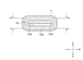
- FIG. 1 illustrates a lighting device including a circuit unit according to an embodiment.
- FIG. 1 is a perspective view illustrating the appearance of a circuit unit according to an embodiment.
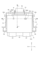
- FIG. 3 is an exploded perspective view illustrating the configuration of the circuit unit in FIG. 2.
- FIG. 2 illustrates an example of the external appearance of the connector viewed from the direction of arrow IV in FIG. 1.
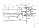
- a cross section taken along line VV in FIG. 4 in the direction of the arrow is illustrated.
- a cross section taken along line VI-VI in FIG. 4 in the direction of the arrow is illustrated.
- a cross section taken along the line VII-VII in FIG. 6 in the direction of the arrow is illustrated.
- a cross section taken along line VIII-VIII in FIG. 6 in the direction of the arrow is illustrated.
- a lighting device including a circuit unit according to another embodiment is illustrated.
- arrow F indicates the forward direction of the illustrated structure.
- Arrow B indicates the rearward direction of the illustrated structure.
- Arrow U indicates the upward direction of the illustrated structure.
- Arrow D indicates the downward direction of the illustrated structure.
- Arrow R indicates the right direction of the illustrated structure.
- Arrow L indicates the left direction of the illustrated structure.
- front-back direction used in this specification means a direction along the above-mentioned front direction and rear direction.
- vertical direction used in this specification means a direction along the above-mentioned upward and downward directions.
- left-right direction used in this specification means a direction along the above-mentioned left direction and right direction.
- extending in the front-back direction includes extending at an angle with respect to the front-back direction, and means extending at an angle closer to the front-back direction than the up-down direction and the left-right direction.
- extending in the vertical direction includes extending at an angle with respect to the up-down direction, and means extending at an inclination closer to the up-down direction than the front-back direction and the left-right direction.
- extending in the left-right direction includes extending at an angle with respect to the left-right direction, and means extending at an inclination closer to the left-right direction than the front-back direction and the up-down direction.
- FIG. 1 schematically illustrates the configuration of a lighting device 10 according to an embodiment.
- the lighting device 10 according to this example is configured to be mounted on a vehicle. There is no limitation on the number of wheels that the vehicle has.
- the vehicle is an example of a moving object.
- the lighting device 10 includes a housing 11 and a transparent cover 12.
- the housing 11 and the light-transmitting cover define a lamp chamber 13.
- the light chamber 13 is an example of a space partitioned by a housing.
- the lighting device 10 includes a lamp unit 14.
- the lamp unit 14 includes a light source 141.
- the light source 141 is configured to emit visible light.
- the light source 141 may be a lamp light source or a semiconductor light emitting device. Examples of semiconductor light emitting devices include light emitting diodes, laser diodes, electroluminescent devices, and the like.
- the light source 141 is configured to emit light including wavelengths in the visible light range. The light emitted from the light source 141 passes through the transparent cover 12 and heads toward the outside of the vehicle.
- the lighting device 10 includes a circuit unit 15.
- the circuit unit 15 includes a board 151 and a connector 152.
- the board 151 is housed within the lamp chamber 13.
- Connector 152 is mounted on board 151.
- the configuration of the circuit unit 15 will be described in detail with reference to FIGS. 2 and 3.
- the circuit unit 15 includes an upper cover 153 and a lower cover 154.
- the upper cover 153 and the lower cover 154 are fastened together by a fastening member 156 so as to sandwich the substrate 151 therebetween.
- the upper cover 153 and the lower cover 154 cover at least a portion of the circuit 155 mounted on the board 151.
- Each of the upper cover 153 and the lower cover 154 is preferably made of metal from the viewpoint of radio wave shielding function for the circuit 155.
- the lower cover 154 may be omitted.
- the circuit unit 15 includes an internal connector 157.
- the circuit 155 is electrically connected to the light source 141 of the lamp unit 14 via an internal connector 157.
- Circuit 155 includes circuit elements for driving light source 141.
- Light source 141 is an example of a driven element.
- FIG. 4 illustrates the configuration seen from the direction of arrow IV in FIG. In the figure, illustration of the back surface 111 is omitted.
- the connector 152 includes a plurality of terminals 152a and a connector housing 152b.
- the connector housing 152b is made of an electrically insulating material.
- the plurality of connector terminals 152a are supported by the connector housing 152b while ensuring mutual electrical insulation.
- the plurality of terminals 152a are arranged in the left-right direction.
- each of the plurality of terminals 152a is made of a conductive material and is electrically connected to the circuit 155.
- all the terminals 152a may be formed of a conductive material and may not be electrically connected to the circuit 155.
- the plurality of terminals 152a may include dummy terminals.
- FIG. 5 schematically illustrates a cross section taken along the line VV in FIG. 4 in the direction of the arrow.
- each terminal 152a has a first portion 152a1.
- the first portion 152a1 extends in the vertical direction.
- the vertical direction is an example of a direction intersecting the substrate 151.
- each via hole 151a has an inner wall covered with a conductive material.
- each via hole 151a is a through hole.
- at least one of the plurality of via holes 151a may be a bottomed hole.
- each terminal 152a is associated with one of the plurality of via holes 151a, and is inserted into the one via hole 151a.
- Each terminal 152a is configured as a press-fit terminal. That is, the first portion 152a1 has a width larger than the width of the corresponding via hole 151a in an initial state, and includes an elastically deformable portion. Therefore, the terminal 152a is inserted into the via hole 151a through press fitting.
- press fitting used in this specification means an operation of inserting a member having a width dimension greater than the width of the hole or recess into a hole or recess.
- the first portion 152a1 is in elastic contact with the inner wall of the via hole 151a. This ensures electrical connection between the terminal 152a and the circuit 155 via the conductive material covering the inner wall of the via hole 151a.
- Each terminal 152a has a second portion 152a2.
- the second portion 152a2 extends in the front-rear direction.
- the front-back direction is an example of a direction along the substrate 151.
- the second portion 152a2 is a portion that is accessible from the outside of the lamp chamber 13 through the opening 112 formed in the housing 11.
- the second portion 152a2 is a portion used for connection with a terminal of a mating connector (not shown).
- the mating connector may be electrically connected to a device located outside the lighting device 10.
- the mating connector may be a jumper connection connector that selectively connects specific terminals to each other.
- the connector housing 152b has a plurality of protrusions 152b1.
- Each convex portion 152b1 extends in the vertical direction. That is, each convex portion 152b1 extends in a direction intersecting the substrate 151. In this example, four convex portions 152b1 are provided. However, one of the protrusions 152b1 may be omitted.
- each fitting hole 151b is a through hole.
- at least one of the plurality of fitting holes 151b may be a bottomed hole.
- each protrusion 152b1 is associated with one of the plurality of fitting holes 151b, and is press-fitted into the one fitting hole 151b.
- the circuit unit 15 can be manufactured by the procedure illustrated below.
- a substrate 151 in which a plurality of via holes 151a and a plurality of fitting holes 151b are formed is prepared.
- the circuit 155 may be mounted on the substrate 151 at this point, or may be mounted in a later process.
- the connector 152 is mounted on the board 151. Specifically, the connector 152 is mounted on the substrate 151 such that the first portion 152a1 of each terminal 152a and each convex portion 152b1 extend in a direction intersecting the substrate 151. As a result, each first portion 152a1 is press-fitted into the corresponding via hole 151a, and each convex portion 152b1 is press-fitted into the corresponding fitting hole 151b at the same time.
- the connector 152 is fixed to the substrate 151 and electrically connected to the circuit 155 by elastic contact of the first portion 152a1 with the inner wall of the via hole 151a and by fitting the convex portion 152b1 into the fitting hole 151b.
- electrical connection with the circuit 155 is ensured by press-fitting the terminal 152a of the connector 152 into the via hole 151a. Since there is no need to additionally use solder, conductive adhesive, screws, etc., it is possible to simplify manufacturing equipment and process control, reduce environmental impact, and reduce the amount of materials used.
- the manufacturing cost of the circuit unit 15 and, by extension, the manufacturing cost of the lighting device 10 including the circuit unit 15 can be reduced.
- the convex portion 152b1 that is press-fitted into the fitting hole 151b formed in the substrate 151 has a circular cross-sectional shape.
- the cross-sectional shape may be any polygonal shape as long as it can be press-fitted into the fitting hole 151b.
- a press-fit terminal having a simple configuration is used as the terminal 152a of the connector 152. This fact can also contribute to reducing the manufacturing cost of the circuit unit 15.
- the configuration of the first portion 152a1 of the terminal 152a press-fitted into the via hole 151a may be changed as appropriate, as long as the electrical connection with the circuit 155 can be ensured by making elastic contact with the inner wall of the via hole 151a.
- the first portion 152a1 may be configured to include a shaft body extending in a direction intersecting the substrate 151, and a movable body biased radially outward of the shaft body by a spring.
- the board 151 of the circuit unit 15 is housed in the housing 11, and the connector 152 is inserted into the opening 112 from the inside of the housing 11. , the circuit unit 15 is mounted on the lighting device 10.
- the lighting device 10 includes a sealing member 16.
- the sealing member 16 is made of an elastic material. The material and shape of the sealing member 16 are determined so as to ensure waterproofness and dustproofness for the lamp chamber 13. Examples of the sealing member 16 include a gasket and an O-ring.
- the sealing member 16 is attached to the connector 152 so as to be disposed between the connector housing 152b and the opening 112.
- the electrical connection between the light source 141 and the circuit unit 15 is made via the internal connector 157.
- the orientation of the conductive terminals included in the internal connector 157 can be determined arbitrarily, it is preferable that the direction corresponds to the direction in which the second portion 152a2 of the terminal 152a in the connector 152 extends.
- the direction in which the connector housing 152b is inserted into the opening 112 of the housing 11 coincides with the direction in which the connector electrically connected to the light source 141 is fitted into the internal connector 157. .
- This improves assembly workability, which can contribute to reducing the manufacturing cost of the lighting device 10.
- FIG. 6 illustrates a cross section taken along the line VI-VI in FIG. 4 in the direction of the arrow.
- the connector housing 152b of the connector 152 has a pair of protrusions 152b2.
- Each convex portion 152b2 extends in the vertical direction.
- a pair of holes 153a are formed in the upper cover 153.
- each protrusion 152b2 engages with one of the corresponding pair of holes 153a.
- the circuit unit 15 includes a fastening member 158.
- the fastening member 158 fixes the circuit unit 15 to the housing 11 by fastening the upper cover 153 to the housing 11.
- the fastening member 158 connects the upper cover 153 to the housing 11 at a position closer to the front edge 151d, which is farther from the connector 152 than the rear edge 151c, which is closer to the connector 152, of both edges in the front-rear direction of the board 151. has concluded.
- the convex portion 152b2 engages with the upper cover 153 at a position closer to the rear edge 151c, which is closer to the connector 152, than the front edge 151d, which is farther from the connector 152, of both edges in the front-rear direction of the board 151. It matches.
- the stress applied to the connector 152 can be released to the upper cover 153 more quickly, so that the local concentration of the stress on the substrate 151 can be easily alleviated.
- FIG. 7 illustrates a cross section taken along line VII-VII in FIG. 6 in the direction of the arrow.
- FIG. 8 illustrates a cross section taken along line VIII-VIII in FIG. 6 in the direction of the arrow.
- the housing 11 has a pair of guide walls 113.
- the pair of guide walls 113 face each other in the left-right direction.
- a guide groove 114 is formed in each guide wall 113.
- the guide groove 114 extends in the front-rear direction. That is, the guide groove 114 extends in the same direction as the direction in which the second portion 152a2 of the terminal 152a of the connector 152 extends.
- the upper cover 153 of the circuit unit 15 has a plurality of collar portions 153b.
- Each collar portion 153b extends in the left-right direction.
- the circuit unit 15 is attached to the housing 11 by being inserted between the pair of guide walls 113 from the front. As illustrated in FIG. 6, the distance between the pair of guide walls 113 in the left-right direction narrows as it approaches the back surface 111. Thereby, the connector 152 is guided to the opening 112 while being positioned in the left-right direction.
- Each guide groove 114 has a pair of inner walls 114a facing each other in the vertical direction. Thereby, the connector 152 is guided to the opening 112 while being positioned in the vertical direction.
- the terminal 152a of the connector 152 can be easily connected to the lamp chamber. It can be made accessible from outside of 13. Since the efficiency of mounting the circuit unit 15 on the housing 11 is increased, the manufacturing cost of the lighting device 10 can be reduced.
- a gap is formed in the vertical direction between the flange 153b of the upper cover 153 and the inner wall 114a of the guide groove 114.
- the up-down direction in this case is an example of a direction intersecting the direction in which the guide groove 114 extends.
- the width of the guide groove 114 in the vertical direction becomes narrower as it approaches the opening 112.
- the pair of inner walls 114a are both formed as inclined surfaces.
- the angle formed by both inclined surfaces may be, for example, 3° to 5°. According to such a configuration, the positioning function of the connector 152 in the above-described vertical direction can be enhanced.
- one of the inner walls 114a may be a flat surface.
- the pair of inner walls 114a face each other in the vertical direction (vertical direction) as in this example, it is preferable that the lower inner wall 114a is a flat surface. According to such a configuration, after the circuit unit 15 is attached to the housing 11, the upper cover 153 can be supported by the lower inner wall 114a, increasing the stability of the structure.
- the pair of protrusions 152b2 formed on the connector housing 152b engage with the upper cover 153 through the pair of holes 153a.
- force can be easily transmitted to the connector 152.
- This configuration is advantageous when the resistance to insertion of the connector 152 is relatively high (eg, when the sealing member 16 is disposed between the connector housing 152b and the opening 112).
- the convex portion 152b2 for releasing external force applied to the connector 152 from the outside to the upper cover 153 is also used to improve the workability of inserting the connector 152 into the opening 112.
- these two functions may be realized by independent engagement structures between the connector 152 and the top cover 153.
- the fastening direction of the upper cover 153 to the housing 11 by the fastening member 158 is arbitrary, it is preferable that the fastening is done along the direction in which the guide groove 114 extends, as illustrated in FIG.
- the direction in which the connector housing 152b is inserted into the opening 112 of the housing 11 coincides with the direction in which the upper cover 153 is fastened to the housing. This increases the efficiency of mounting the circuit unit 15 on the housing 11, which can contribute to reducing the manufacturing cost of the lighting device 10.
- the first portion 152a1 of the terminal 152a in the connector 152 extends in a direction along the substrate 151.
- the attitude of the board 151 and the attitude of the connector 152 can have a relationship as illustrated in FIG. 9 .
- both the first portion 152a1 and the second portion 152a2 of the terminal 152a extend in a direction intersecting the substrate 151.
- the connector 152 of the circuit unit 15 is inserted into the opening 112 formed in the back surface 111 of the housing 11.
- the position of the opening 112 can be determined as appropriate depending on the specifications of the lighting device 10.
- the relationship between the posture of the board 151 and the posture of the connector 152 can also be determined as appropriate.
- the circuit 155 mounted on the board 151 of the circuit unit 15 is electrically connected to the light source 141 of the lamp unit 14.
- the circuit 155 includes a device that dissipates heat generated from the light source 141, a device that changes the direction of light emitted from the light source 141, a device that changes the light distribution pattern formed by the light emitted from the light source 141, etc. may be electrically connected to. These devices are also examples of driven elements.
- the circuit unit 15 does not need to be mounted on the lighting device 10.
- the circuit 155 may control the operation of a sensor housed in a space defined by the housing 11. That is, the circuit unit 15 can be installed in a sensor device for acquiring predetermined information.
- sensors include a LiDAR (Light Detection and Ranging) sensor, a camera, a millimeter wave radar, an ultrasonic sensor, a temperature sensor, and the like. These sensors are also examples of driven elements.
- the lighting device 10 and the sensor device described above may be mounted on a moving object other than a vehicle.
- Examples of other moving objects include aircraft, flying objects, ships, and the like.
- the mobile object may not require a driver.
- the lighting device 10 and the sensor device described above do not need to be mounted on a moving body.
- the lighting device 10 and the sensor device described above can also be applied to a system that is installed in a house, facility, transportation infrastructure, etc. and operates in response to an object that enters a specific area.
- the lighting device 10 can also be applied to a device that temporarily displays predetermined figures, characters, signs, etc. on a specific road surface or wall surface.
- the circuit unit 15 does not need to be electrically connected to a specific driven element.
- the housing 11 having the opening 112 can function as a housing structure for the circuit unit 15. According to the configuration of the present disclosure, the manufacturing cost of the accommodation structure can also be reduced.
- Japanese Patent Application No. 2022-044215 filed on March 18, 2022
- Japanese Patent Application No. 2022-044216 filed on March 18, 2022
- the contents of Japanese Patent Application No. 2022-044217 filed on March 18, 2022 are incorporated.
Abstract
A connector (152) is mounted on a substrate (151) on which a circuit has been mounted. The connector (152) includes a terminal (152a) and a connector housing (152b). The terminal (152a) is electrically connected to the circuit. The connector housing (152b) supports the terminal (152a). The terminal (152a) includes a first portion (152a1) which extends in a direction intersecting the substrate (151) and is in elastic contact with an inner wall of a bore hole (151a) formed in the substrate (151). The connector housing (152b) includes a protrusion (152b1) which extends in the direction intersecting the substrate (151) and which is fitted into a fitting hole (151b) formed in the substrate (151).
Description
本開示は、回路ユニットとその製造方法に関連する。本開示は、当該回路ユニットを収容する構造にも関連する。本開示は、当該回路ユニットを備えた装置にも関連する。
The present disclosure relates to a circuit unit and a method for manufacturing the same. The present disclosure also relates to a structure housing the circuit unit. The present disclosure also relates to a device including the circuit unit.
特許文献1は、移動体の一例としての車両に搭載される装置の一例としてのヘッドランプを開示している。当該ヘッドランプは、ハウジングに収容された光源の動作を制御する制御回路を含む回路ユニットを備えている。当該制御回路と内側コネクタが搭載された基板は、外側コネクタを備えた筐体に収容されている。制御回路と内側コネクタおよび外側コネクタとの電気的接続は、はんだ付けを通じてなされる。筐体は、ハウジングの外側面に配置される。制御回路と光源との電気的接続は、内側コネクタを通じてなされる。制御回路と外部装置との電気的接続は、外側コネクタを通じてなされる。
Patent Document 1 discloses a headlamp as an example of a device mounted on a vehicle as an example of a moving object. The headlamp includes a circuit unit including a control circuit for controlling the operation of a light source housed in a housing. The board on which the control circuit and the inner connector are mounted is housed in a casing equipped with an outer connector. Electrical connections between the control circuit and the inner and outer connectors are made through soldering. The casing is arranged on the outer surface of the housing. Electrical connection between the control circuit and the light source is made through the inner connector. Electrical connections between the control circuit and external devices are made through the outer connector.
回路ユニット、当該回路ユニットを収容する構造、および当該回路ユニットを備えた装置の製造コストを低減することが求められている。
There is a need to reduce the manufacturing costs of circuit units, structures that house the circuit units, and devices equipped with the circuit units.
本開示により提供される第一の態様例は、回路ユニットであって、
回路が搭載されている基板と、
前記基板に搭載されているコネクタと、
を備えており、
前記コネクタは、
前記回路と電気的に接続されている導電端子と、
前記導電端子を支持しているコネクタハウジングと、
を備えており、
前記導電端子は、前記基板と交差する方向に延びており、かつ前記基板に形成されたビアホールの内壁に弾性接触している部分を有しており、
前記コネクタハウジングは、前記基板と交差する方向に延びており、かつ前記基板に形成された穴に嵌入された凸部を有している。 A first embodiment provided by the present disclosure is a circuit unit that includes:
A board on which the circuit is mounted,
a connector mounted on the board;
It is equipped with
The connector is
a conductive terminal electrically connected to the circuit;
a connector housing supporting the conductive terminal;
It is equipped with
The conductive terminal extends in a direction intersecting the substrate, and has a portion that is in elastic contact with an inner wall of a via hole formed in the substrate,
The connector housing extends in a direction intersecting the substrate and has a protrusion fitted into a hole formed in the substrate.
第一の態様例に係る構成によれば、コネクタの導電端子をビアホールに圧入することによって回路との電気的接続が確保される。はんだ、導電性接着剤、スクリュウなどを付加的に使用する必要がないので、製造設備や工程管理の簡略化、環境負荷の軽減、材料の低減などが可能である。
According to the configuration according to the first aspect, electrical connection with the circuit is ensured by press-fitting the conductive terminal of the connector into the via hole. Since there is no need to additionally use solder, conductive adhesive, screws, etc., it is possible to simplify manufacturing equipment and process control, reduce environmental impact, and reduce the amount of materials used.
他方、はんだ、導電性接着剤、スクリュウなどを使用しないことにより、基板による導電端子の支持強度の低下は避けられない。しかしながら、導電端子を支持するコネクタハウジングに設けられた凸部が基板に形成された穴に圧入されるので、支持強度の低下が補われうる。加えて、導電端子と凸部が基板に対して同じ方向かつ同時に圧入されるので、支持強度の低下を補うための別部品、別設備、および別工程の少なくとも一つの追加を不要にできる。
On the other hand, by not using solder, conductive adhesive, screws, etc., a decrease in the support strength of the conductive terminal by the substrate is inevitable. However, since the protrusion provided on the connector housing that supports the conductive terminal is press-fitted into the hole formed in the substrate, the reduction in support strength can be compensated for. In addition, since the conductive terminal and the convex portion are press-fitted into the substrate in the same direction and at the same time, it is possible to eliminate the need for at least one additional part, separate equipment, and separate process to compensate for the reduction in support strength.
結果として、回路ユニットの製造コスト、ひいては当該回路ユニットを収容する構造や当該回路ユニットを装置の製造コストを低減できる。
As a result, the manufacturing cost of the circuit unit, as well as the manufacturing cost of the structure housing the circuit unit and the device using the circuit unit, can be reduced.
したがって、本開示により提供される第二の態様例は、回路ユニットの製造方法であって、
回路が搭載される基板を用意する工程と、
前記回路と電気的に接続される導電端子、当該導電端子を支持するコネクタハウジング、および当該コネクタハウジングに形成された凸部を備えたコネクタを用意する工程と、
前記導電端子と前記凸部が前記基板と交差する向きに延びるように前記コネクタを前記基板に搭載することにより、前記導電端子を前記基板に形成されたビアホールの内壁に弾性接触させるとともに、前記凸部を前記基板に形成された穴に嵌入させる工程と、
を含んでいる。 Therefore, a second example embodiment provided by the present disclosure is a method for manufacturing a circuit unit, comprising:
A step of preparing a board on which the circuit is mounted;
preparing a connector including a conductive terminal that is electrically connected to the circuit, a connector housing that supports the conductive terminal, and a convex portion formed on the connector housing;
By mounting the connector on the substrate so that the conductive terminal and the convex portion extend in a direction intersecting the substrate, the conductive terminal is brought into elastic contact with the inner wall of a via hole formed in the substrate, and the convex portion extends in a direction intersecting the substrate. a step of fitting the part into a hole formed in the substrate;
Contains.
したがって、本開示により提供される第三の態様例は、回路ユニットの収容構造であって、
空間を区画しているハウジングと、
回路ユニットと、
を含んでおり、
前記回路ユニットは、
前記空間に収容されており、回路が搭載されている基板と、
前記基板に搭載されているコネクタと、
を備えており、
前記コネクタは、
前記回路と電気的に接続されている導電端子と、
前記導電端子を支持しているコネクタハウジングと、
を備えており、
前記導電端子は、
前記基板と交差する第一方向に延びており、かつ前記基板に形成されたビアホールの内壁に弾性接触している第一部分と、
第二方向に延びており、かつ前記ハウジングに形成された開口を通じて前記空間の外側からアクセス可能である第二部分と、
を有しており、
前記コネクタハウジングは、前記第一方向に延びており、かつ前記基板に形成された穴に嵌入された凸部を有している。 Therefore, the third embodiment provided by the present disclosure is a housing structure for a circuit unit, comprising:
A housing that divides the space,
a circuit unit;
It contains
The circuit unit is
a board housed in the space and on which a circuit is mounted;
a connector mounted on the board;
It is equipped with
The connector is
a conductive terminal electrically connected to the circuit;
a connector housing supporting the conductive terminal;
It is equipped with
The conductive terminal is
a first portion extending in a first direction intersecting the substrate and in elastic contact with an inner wall of a via hole formed in the substrate;
a second portion extending in a second direction and accessible from outside the space through an opening formed in the housing;
It has
The connector housing has a protrusion extending in the first direction and fitted into a hole formed in the substrate.
したがって、本開示により提供される第四の態様例は、装置であって、
被駆動要素と、
空間を区画しているハウジングと、
前記被駆動要素と電気的に接続された回路を備えている回路ユニットと、
を備えており、
前記回路ユニットは、
前記空間に収容されており、前記回路が搭載されている基板と、
前記基板に搭載されているコネクタと、
を備えており、
前記コネクタは、
前記回路と電気的に接続されている導電端子と、
前記導電端子を支持しているコネクタハウジングと、
を備えており、
前記導電端子は、
前記基板と交差する第一方向に延びており、かつ前記基板に形成されたビアホールの内壁に弾性接触している第一部分と、
第二方向に延びており、かつ前記ハウジングに形成された開口を通じて前記空間の外側からアクセス可能である第二部分と、
を有しており、
前記コネクタハウジングは、前記第一方向に延びており、かつ前記基板に形成された穴に嵌入された凸部を有している。 Accordingly, a fourth example aspect provided by the present disclosure is an apparatus comprising:
a driven element;
A housing that divides the space,
a circuit unit comprising a circuit electrically connected to the driven element;
It is equipped with
The circuit unit is
a board accommodated in the space and on which the circuit is mounted;
a connector mounted on the board;
It is equipped with
The connector is
a conductive terminal electrically connected to the circuit;
a connector housing supporting the conductive terminal;
It is equipped with
The conductive terminal is
a first portion extending in a first direction intersecting the substrate and in elastic contact with an inner wall of a via hole formed in the substrate;
a second portion extending in a second direction and accessible from outside the space through an opening formed in the housing;
It has
The connector housing has a protrusion extending in the first direction and fitted into a hole formed in the substrate.
本開示により提供される第五の態様例は、回路ユニットの収容構造であって、
空間を区画しているハウジングと、
回路ユニットと、
を含んでおり、
前記回路ユニットは、
前記空間に収容されており、回路が搭載されている基板と、
前記基板に搭載されているコネクタと、
前記回路の少なくとも一部を覆い、かつ前記コネクタと係合しているカバーと、
前記カバーを前記ハウジングに締結している締結部材と、
を備えており、
前記コネクタは、前記回路と電気的に接続された導電端子を備えており、
前記導電端子は、前記基板に沿う第一方向に延びており、かつ前記ハウジングに形成された開口を通じて前記空間の外側からアクセス可能である部分を有しており、
前記締結部材は、前記基板の前記第一方向における両端縁のうち、前記コネクタにより近い端縁よりも前記コネクタからより遠い端縁に近い位置において前記カバーを前記ハウジングに締結している。 A fifth aspect example provided by the present disclosure is a housing structure for a circuit unit, comprising:
A housing that divides the space,
a circuit unit;
It contains
The circuit unit is
a board housed in the space and on which a circuit is mounted;
a connector mounted on the board;
a cover covering at least a portion of the circuit and engaging the connector;
a fastening member fastening the cover to the housing;
It is equipped with
The connector includes a conductive terminal electrically connected to the circuit,
The conductive terminal extends in a first direction along the substrate and has a portion that is accessible from outside the space through an opening formed in the housing,
The fastening member fastens the cover to the housing at a position closer to an edge farther from the connector than an edge closer to the connector among both edges of the board in the first direction.
本開示により提供される第六の態様例は、装置であって、
被駆動要素と、
空間を区画しているハウジングと、
前記被駆動要素と電気的に接続された回路を備えている回路ユニットと、
を備えており、
前記回路ユニットは、
前記空間に収容されており、前記回路が搭載されている基板と、
前記基板に搭載されているコネクタと、
前記回路の少なくとも一部を覆い、かつ前記コネクタと係合しているカバーと、
前記カバーを前記ハウジングに締結している締結部材と、
を備えており、
前記コネクタは、前記回路と電気的に接続された導電端子を備えており、
前記導電端子は、前記基板に沿う第一方向に延びており、かつ前記ハウジングに形成された開口を通じて前記空間の外側からアクセス可能である部分を有しており、
前記締結部材は、前記基板の前記第一方向における両端縁のうち、前記コネクタにより近い端縁よりも前記コネクタからより遠い端縁に近い位置において前記カバーを前記ハウジングに締結している。 A sixth aspect provided by the present disclosure is an apparatus, the device comprising:
a driven element;
A housing that divides the space,
a circuit unit comprising a circuit electrically connected to the driven element;
It is equipped with
The circuit unit is
a board accommodated in the space and on which the circuit is mounted;
a connector mounted on the board;
a cover covering at least a portion of the circuit and engaging the connector;
a fastening member fastening the cover to the housing;
It is equipped with
The connector includes a conductive terminal electrically connected to the circuit,
The conductive terminal extends in a first direction along the substrate and has a portion that is accessible from outside the space through an opening formed in the housing,
The fastening member fastens the cover to the housing at a position closer to an edge farther from the connector than an edge closer to the connector among both edges of the board in the first direction.
例えば相手側コネクタとの嵌合時において、コネクタには外部から応力が加わる。第五の態様例および第六の態様例の各々に係る構成によれば、当該応力はコネクタと係合しているカバーに伝達され、コネクタから比較的離れたハウジングとの締結位置においてハウジングへと逃がされる。これにより、コネクタに加えられた応力が基板へ局所的に集中しにくくできる。
For example, when mating with a mating connector, stress is applied to the connector from the outside. According to the configuration according to each of the fifth aspect and the sixth aspect, the stress is transmitted to the cover that engages with the connector, and is transmitted to the housing at the fastening position with the housing that is relatively far from the connector. be let go. This makes it difficult for stress applied to the connector to be locally concentrated on the board.
したがって、コネクタに加わる外部応力から基板に搭載された回路を保護するための別部品、別設備、および別工程の少なくとも一つを不要にできる。結果として、回路ユニットを収容する構造や回路ユニットを備えた装置の製造コストを低減できる。
Therefore, at least one of a separate part, separate equipment, and separate process for protecting the circuit mounted on the board from external stress applied to the connector can be eliminated. As a result, it is possible to reduce the manufacturing cost of a structure accommodating the circuit unit and a device equipped with the circuit unit.
本開示により提供される第七の態様例は、回路ユニットの収容構造であって、
空間を区画しているハウジングと、
回路ユニットと、
を含んでおり、
前記回路ユニットは、
前記空間に収容されており、回路が搭載されている基板と、
前記基板に搭載されているコネクタと、
前記回路の少なくとも一部を覆っているカバーと、
を備えており、
前記コネクタは、前記回路と電気的に接続された導電端子を備えており、
前記導電端子は、第一方向に延びており、かつ前記ハウジングに形成された開口を通じて前記空間の外側からアクセス可能である部分を有しており、
前記ハウジングは、前記第一方向に延びる案内溝を有しており、
前記カバーは、前記案内溝に配置された鍔部を有している。 A seventh aspect provided by the present disclosure is a circuit unit housing structure, comprising:
A housing that divides the space,
a circuit unit;
It contains
The circuit unit is
a board housed in the space and on which a circuit is mounted;
a connector mounted on the board;
a cover covering at least a portion of the circuit;
It is equipped with
The connector includes a conductive terminal electrically connected to the circuit,
The conductive terminal extends in a first direction and has a portion that is accessible from outside the space through an opening formed in the housing;
The housing has a guide groove extending in the first direction,
The cover has a flange disposed in the guide groove.
本開示により提供される第八の態様例は、装置であって、
被駆動要素と、
空間を区画しているハウジングと、
前記被駆動要素と電気的に接続された回路を備えている回路ユニットと、
を備えており、
前記回路ユニットは、
前記空間に収容されており、前記回路が搭載されている基板と、
前記基板に搭載されているコネクタと、
前記回路の少なくとも一部を覆っているカバーと、
を備えており、
前記コネクタは、前記回路と電気的に接続された導電端子を備えており、
前記導電端子は、第一方向に延びており、かつ前記ハウジングに形成された開口を通じて前記空間の外側からアクセス可能である部分を有しており、
前記ハウジングは、前記第一方向に延びる案内溝を有しており、
前記カバーは、前記案内溝に配置された鍔部を有している。 An eighth example aspect provided by the present disclosure is an apparatus comprising:
a driven element;
A housing that divides the space,
a circuit unit comprising a circuit electrically connected to the driven element;
It is equipped with
The circuit unit is
a board accommodated in the space and on which the circuit is mounted;
a connector mounted on the board;
a cover covering at least a portion of the circuit;
It is equipped with
The connector includes a conductive terminal electrically connected to the circuit,
The conductive terminal extends in a first direction and has a portion that is accessible from outside the space through an opening formed in the housing;
The housing has a guide groove extending in the first direction,
The cover has a flange disposed in the guide groove.
第七の態様例および第八の態様例の各々に係る構成によれば、コネクタの端子における空間の外部からのアクセスに供される部分と同じ方向に延びる案内溝に沿って回路ユニットを摺動させることによって、容易に端子の当該部分を空間の外部からアクセス可能な状態にできる。回路ユニットをハウジングに搭載する作業の効率が高まるので、当該回路ユニットを収容する構造、および当該回路ユニットを備えた装置の製造コストを低減できる。
According to the configuration according to each of the seventh aspect and the eighth aspect, the circuit unit is slidable along the guide groove extending in the same direction as the portion of the terminal of the connector that is accessed from the outside of the space. By doing so, the corresponding portion of the terminal can be easily made accessible from outside the space. Since the efficiency of mounting the circuit unit in the housing is increased, it is possible to reduce the manufacturing cost of a structure accommodating the circuit unit and a device equipped with the circuit unit.
添付の図面を参照しつつ、実施形態の例について以下詳細に説明する。以下の説明に用いられる各図面では、各部材を認識可能な大きさとするために、必要に応じて縮尺を変更している。
Examples of embodiments will be described in detail below with reference to the accompanying drawings. In each of the drawings used in the following description, the scale is changed as necessary to make each member recognizable in size.
添付の図面において、矢印Fは、図示された構造の前方向を示している。矢印Bは、図示された構造の後方向を示している。矢印Uは、図示された構造の上方向を示している。矢印Dは、図示された構造の下方向を示している。矢印Rは、図示された構造の右方向を示している。矢印Lは、図示された構造の左方向を示している。これらの方向に係る表現は、説明の便宜のために用いることを意図しており、当該構造の実使用時における姿勢を限定することを意図してはいない。
In the accompanying drawings, arrow F indicates the forward direction of the illustrated structure. Arrow B indicates the rearward direction of the illustrated structure. Arrow U indicates the upward direction of the illustrated structure. Arrow D indicates the downward direction of the illustrated structure. Arrow R indicates the right direction of the illustrated structure. Arrow L indicates the left direction of the illustrated structure. These directional expressions are intended to be used for convenience of explanation, and are not intended to limit the orientation of the structure in actual use.
本明細書で用いられる「前後方向」という語は、上記の前方向と後方向に沿う方向を意味している。本明細書で用いられる「上下方向」という語は、上記の上方向と下方向に沿う方向を意味している。本明細書で用いられる「左右方向」という語は、上記の左方向と右方向に沿う方向を意味している。
The term "front-back direction" used in this specification means a direction along the above-mentioned front direction and rear direction. The term "vertical direction" used in this specification means a direction along the above-mentioned upward and downward directions. The term "left-right direction" used in this specification means a direction along the above-mentioned left direction and right direction.
本明細書で用いられる「前後方向に延びる」という表現は、前後方向に対して傾いて延びることを含み、上下方向および左右方向と比較して前後方向に近い傾きで伸びることを意味する。
The expression "extending in the front-back direction" used in this specification includes extending at an angle with respect to the front-back direction, and means extending at an angle closer to the front-back direction than the up-down direction and the left-right direction.
本明細書で用いられる「上下方向に延びる」という表現は、上下方向に対して傾いて延びることを含み、前後方向および左右方向と比較して上下方向に近い傾きで伸びることを意味する。
The expression "extending in the vertical direction" used in this specification includes extending at an angle with respect to the up-down direction, and means extending at an inclination closer to the up-down direction than the front-back direction and the left-right direction.
本明細書で用いられる「左右方向に延びる」という表現は、左右方向に対して傾いて延びることを含み、前後方向および上下方向と比較して左右方向に近い傾きで伸びることを意味する。
The expression "extending in the left-right direction" used in this specification includes extending at an angle with respect to the left-right direction, and means extending at an inclination closer to the left-right direction than the front-back direction and the up-down direction.
図1は、一実施形態に係る照明装置10の構成を模式的に例示している。本例に係る照明装置10は、車両に搭載されるように構成されている。当該車両が備えている車輪の数についての限定はない。当該車両は、移動体の一例である。
FIG. 1 schematically illustrates the configuration of a lighting device 10 according to an embodiment. The lighting device 10 according to this example is configured to be mounted on a vehicle. There is no limitation on the number of wheels that the vehicle has. The vehicle is an example of a moving object.
照明装置10は、ハウジング11と透光カバー12を備えている。ハウジング11は、透光カバーとともに灯室13を区画している。灯室13は、ハウジングにより区画される空間の一例である。
The lighting device 10 includes a housing 11 and a transparent cover 12. The housing 11 and the light-transmitting cover define a lamp chamber 13. The light chamber 13 is an example of a space partitioned by a housing.
照明装置10は、灯具ユニット14を備えている。灯具ユニット14は、光源141を備えている。光源141は、可視光を出射するように構成されている。光源141は、ランプ光源であってもよいし、半導体発光素子であってもよい。半導体発光素子の例としては、発光ダイオード、レーザダイオード、エレクトロルミネッセンス素子などが挙げられる。光源141は、可視光域の波長を含む光を出射するように構成されている。光源141から出射された光は、透光カバー12を通過して車両の外方へ向かう。
The lighting device 10 includes a lamp unit 14. The lamp unit 14 includes a light source 141. The light source 141 is configured to emit visible light. The light source 141 may be a lamp light source or a semiconductor light emitting device. Examples of semiconductor light emitting devices include light emitting diodes, laser diodes, electroluminescent devices, and the like. The light source 141 is configured to emit light including wavelengths in the visible light range. The light emitted from the light source 141 passes through the transparent cover 12 and heads toward the outside of the vehicle.
照明装置10は、回路ユニット15を備えている。回路ユニット15は、基板151とコネクタ152を備えている。基板151は、灯室13内に収容されている。コネクタ152は、基板151に搭載されている。
The lighting device 10 includes a circuit unit 15. The circuit unit 15 includes a board 151 and a connector 152. The board 151 is housed within the lamp chamber 13. Connector 152 is mounted on board 151.
図2と図3を参照しつつ、回路ユニット15の構成について詳細に説明する。回路ユニット15は、上カバー153と下カバー154を備えている。上カバー153と下カバー154は、締結部材156により基板151を挟むように締結されている。これにより、上カバー153と下カバー154は、基板151に搭載された回路155の少なくとも一部を覆っている。上カバー153と下カバー154の各々は、回路155に対する電波シールド機能の観点から、金属製であることが好ましい。下カバー154は省略されうる。
The configuration of the circuit unit 15 will be described in detail with reference to FIGS. 2 and 3. The circuit unit 15 includes an upper cover 153 and a lower cover 154. The upper cover 153 and the lower cover 154 are fastened together by a fastening member 156 so as to sandwich the substrate 151 therebetween. As a result, the upper cover 153 and the lower cover 154 cover at least a portion of the circuit 155 mounted on the board 151. Each of the upper cover 153 and the lower cover 154 is preferably made of metal from the viewpoint of radio wave shielding function for the circuit 155. The lower cover 154 may be omitted.
回路ユニット15は、内部コネクタ157を備えている。回路155は、内部コネクタ157を介して灯具ユニット14の光源141と電気的に接続されている。回路155は、光源141を駆動するための回路要素を含んでいる。光源141は、被駆動要素の一例である。
The circuit unit 15 includes an internal connector 157. The circuit 155 is electrically connected to the light source 141 of the lamp unit 14 via an internal connector 157. Circuit 155 includes circuit elements for driving light source 141. Light source 141 is an example of a driven element.
図1に例示されるように、ハウジング11の背面111には開口112が形成されている。回路ユニット15のコネクタ152の一部は、開口112内に配置されている。図4は、図1における矢印IV方向から見た構成を例示している。同図においては、背面111の図示は省略されている。
As illustrated in FIG. 1, an opening 112 is formed in the back surface 111 of the housing 11. A portion of the connector 152 of the circuit unit 15 is disposed within the opening 112. FIG. 4 illustrates the configuration seen from the direction of arrow IV in FIG. In the figure, illustration of the back surface 111 is omitted.
コネクタ152は、複数の端子152aとコネクタハウジング152bを備えている。コネクタハウジング152bは、電気的絶縁性を有する材料により形成されている。コネ複数の端子152aは、相互に電気的絶縁性を確保された状態で、コネクタハウジング152bにより支持されている。複数の端子152aは、左右方向に配列されている。
The connector 152 includes a plurality of terminals 152a and a connector housing 152b. The connector housing 152b is made of an electrically insulating material. The plurality of connector terminals 152a are supported by the connector housing 152b while ensuring mutual electrical insulation. The plurality of terminals 152a are arranged in the left-right direction.
本例においては、複数の端子152aの各々は、導電性を有する材料により形成されており、かつ回路155と電気的に接続されている。しかしながら、全ての端子152aが導電性を有する材料により形成され、かつ回路155と電気的に接続されていなくともよい。換言すると、複数の端子152aは、ダミー端子を含みうる。
In this example, each of the plurality of terminals 152a is made of a conductive material and is electrically connected to the circuit 155. However, all the terminals 152a may be formed of a conductive material and may not be electrically connected to the circuit 155. In other words, the plurality of terminals 152a may include dummy terminals.
図5は、図4における線V-Vに沿って矢印方向から見た断面を模式的に例示している。図3と図5に例示されるように、各端子152aは、第一部分152a1を有している。第一部分152a1は、上下方向に延びている。上下方向は、基板151と交差する方向の一例である。
FIG. 5 schematically illustrates a cross section taken along the line VV in FIG. 4 in the direction of the arrow. As illustrated in FIGS. 3 and 5, each terminal 152a has a first portion 152a1. The first portion 152a1 extends in the vertical direction. The vertical direction is an example of a direction intersecting the substrate 151.
基板151には、複数のビアホール151aが形成されている。本例においては、各ビアホール151aは、導電性を有する材料で覆われた内壁を有している。本例においては、各ビアホール151aは、貫通穴である。しかしながら、複数のビアホール151aの少なくとも一つは、有底穴であってもよい。
A plurality of via holes 151a are formed in the substrate 151. In this example, each via hole 151a has an inner wall covered with a conductive material. In this example, each via hole 151a is a through hole. However, at least one of the plurality of via holes 151a may be a bottomed hole.
各端子152aの第一部分152a1は、複数のビアホール151aの一つに対応付けられており、当該一つのビアホール151aに挿入されている。
The first portion 152a1 of each terminal 152a is associated with one of the plurality of via holes 151a, and is inserted into the one via hole 151a.
各端子152aは、プレスフィット端子として構成されている。すなわち、第一部分152a1は、初期状態において対応するビアホール151aの幅寸法よりも大きな幅寸法を有し、かつ弾性変形可能な部分を含んでいる。したがって、端子152aのビアホール151aへの挿入は、圧入を通じてなされる。
Each terminal 152a is configured as a press-fit terminal. That is, the first portion 152a1 has a width larger than the width of the corresponding via hole 151a in an initial state, and includes an elastically deformable portion. Therefore, the terminal 152a is inserted into the via hole 151a through press fitting.
なお、本明細書において用いられる「圧入」という表現は、穴または凹部に対して当該穴または凹部の幅以上の幅寸法を有する部材を挿入する操作を意味する。
Note that the expression "press fitting" used in this specification means an operation of inserting a member having a width dimension greater than the width of the hole or recess into a hole or recess.
結果として、第一部分152a1は、ビアホール151aの内壁に弾性接触している。これにより、ビアホール151aの内壁を覆う導電性材料を介して、端子152aと回路155との電気的接続が確保される。
As a result, the first portion 152a1 is in elastic contact with the inner wall of the via hole 151a. This ensures electrical connection between the terminal 152a and the circuit 155 via the conductive material covering the inner wall of the via hole 151a.
各端子152aは、第二部分152a2を有している。第二部分152a2は、前後方向に延びている。前後方向は、基板151に沿う方向の一例である。第二部分152a2は、ハウジング11に形成された開口112を通じて灯室13の外側からアクセス可能である部分である。
Each terminal 152a has a second portion 152a2. The second portion 152a2 extends in the front-rear direction. The front-back direction is an example of a direction along the substrate 151. The second portion 152a2 is a portion that is accessible from the outside of the lamp chamber 13 through the opening 112 formed in the housing 11.
第二部分152a2は、不図示の相手側コネクタの端子との結合に供される部分である。一例として、相手側コネクタは、照明装置10の外部に位置する装置と電気的に接続されうる。別例として、相手側コネクタは、特定の端子同士を選択的に導通させるジャンパ接続用コネクタでありうる。
The second portion 152a2 is a portion used for connection with a terminal of a mating connector (not shown). As an example, the mating connector may be electrically connected to a device located outside the lighting device 10. As another example, the mating connector may be a jumper connection connector that selectively connects specific terminals to each other.
図3に例示されるように、コネクタハウジング152bは、複数の凸部152b1を有している。各凸部152b1は、上下方向に延びている。すなわち、各凸部152b1は、基板151と交差する向きに延びている。本例においては、四つの凸部152b1が設けられている。しかしながら、いずれか一つの凸部152b1は省略されうる。
As illustrated in FIG. 3, the connector housing 152b has a plurality of protrusions 152b1. Each convex portion 152b1 extends in the vertical direction. That is, each convex portion 152b1 extends in a direction intersecting the substrate 151. In this example, four convex portions 152b1 are provided. However, one of the protrusions 152b1 may be omitted.
他方、基板151には複数の嵌合穴151bが形成されている。本例においては、各嵌合穴151bは、貫通穴である。しかしながら、複数の嵌合穴151bの少なくとも一つは、有底穴であってもよい。
On the other hand, a plurality of fitting holes 151b are formed in the substrate 151. In this example, each fitting hole 151b is a through hole. However, at least one of the plurality of fitting holes 151b may be a bottomed hole.
図5に例示されるように、各凸部152b1は、複数の嵌合穴151bの一つに対応付けられており、当該一つの嵌合穴151bに圧入されている。
As illustrated in FIG. 5, each protrusion 152b1 is associated with one of the plurality of fitting holes 151b, and is press-fitted into the one fitting hole 151b.
上述した構成を有することにより、回路ユニット15は、以下に例示される手順で製造されうる。
By having the above-described configuration, the circuit unit 15 can be manufactured by the procedure illustrated below.
まず、複数のビアホール151aと複数の嵌合穴151bが形成された基板151が用意される。回路155は、この時点で基板151に搭載されていてもよいし、後の工程で搭載されてもよい。
First, a substrate 151 in which a plurality of via holes 151a and a plurality of fitting holes 151b are formed is prepared. The circuit 155 may be mounted on the substrate 151 at this point, or may be mounted in a later process.
続いて、コネクタ152が基板151に搭載される。具体的には、各端子152aの第一部分152a1と各凸部152b1が基板151と交差する向きに延びるように、コネクタ152の基板151への搭載がなされる。これにより、各第一部分152a1の対応するビアホール151aへの圧入と、各凸部152b1の対応する嵌合穴151bへの圧入とが同時になされる。第一部分152a1のビアホール151aの内壁への弾性接触、および凸部152b1の嵌合穴151bへの嵌入により、コネクタ152の基板151への固定と回路155への電気的接続がなされる。
Subsequently, the connector 152 is mounted on the board 151. Specifically, the connector 152 is mounted on the substrate 151 such that the first portion 152a1 of each terminal 152a and each convex portion 152b1 extend in a direction intersecting the substrate 151. As a result, each first portion 152a1 is press-fitted into the corresponding via hole 151a, and each convex portion 152b1 is press-fitted into the corresponding fitting hole 151b at the same time. The connector 152 is fixed to the substrate 151 and electrically connected to the circuit 155 by elastic contact of the first portion 152a1 with the inner wall of the via hole 151a and by fitting the convex portion 152b1 into the fitting hole 151b.
本実施形態に係る構成によれば、コネクタ152の端子152aをビアホール151aに圧入することによって回路155との電気的接続が確保される。はんだ、導電性接着剤、スクリュウなどを付加的に使用する必要がないので、製造設備や工程管理の簡略化、環境負荷の軽減、材料の低減などが可能である。
According to the configuration according to the present embodiment, electrical connection with the circuit 155 is ensured by press-fitting the terminal 152a of the connector 152 into the via hole 151a. Since there is no need to additionally use solder, conductive adhesive, screws, etc., it is possible to simplify manufacturing equipment and process control, reduce environmental impact, and reduce the amount of materials used.
他方、はんだ、導電性接着剤、スクリュウなどを使用しないことにより、基板151による端子152aの支持強度の低下は避けられない。しかしながら、端子152aを支持するコネクタハウジング152bに設けられた凸部152b1が基板151に形成された嵌合穴151bに圧入されるので、支持強度の低下が補われうる。加えて、端子152aと凸部152b1が基板151に対して同じ方向かつ同時に圧入されるので、支持強度の低下を補うための別部品、別設備、および別工程の少なくとも一つの追加を不要にできる。
On the other hand, by not using solder, conductive adhesive, screws, etc., a decrease in the support strength of the terminal 152a by the substrate 151 is unavoidable. However, since the convex portion 152b1 provided on the connector housing 152b that supports the terminal 152a is press-fitted into the fitting hole 151b formed in the substrate 151, the decrease in support strength can be compensated for. In addition, since the terminal 152a and the convex portion 152b1 are press-fitted into the substrate 151 in the same direction and at the same time, it is possible to eliminate the need for at least one additional part, separate equipment, and separate process to compensate for the reduction in support strength. .
結果として、回路ユニット15の製造コスト、ひいては回路ユニット15を備えた照明装置10の製造コストを低減できる。
As a result, the manufacturing cost of the circuit unit 15 and, by extension, the manufacturing cost of the lighting device 10 including the circuit unit 15 can be reduced.
図5に例示されるように、基板151に形成された嵌合穴151bに圧入される凸部152b1は、円形の断面形状を有している。しかしながら、嵌合穴151bに対する圧入が成立するのであれば、断面形状は任意の多角形状でありうる。
As illustrated in FIG. 5, the convex portion 152b1 that is press-fitted into the fitting hole 151b formed in the substrate 151 has a circular cross-sectional shape. However, the cross-sectional shape may be any polygonal shape as long as it can be press-fitted into the fitting hole 151b.
本実施形態においては、コネクタ152の端子152aとして簡易な構成を有するプレスフィット端子が用いられている。この事実もまた回路ユニット15の製造コストの低減に寄与しうる。
In this embodiment, a press-fit terminal having a simple configuration is used as the terminal 152a of the connector 152. This fact can also contribute to reducing the manufacturing cost of the circuit unit 15.
しかしながら、ビアホール151aの内壁に対して弾性接触することによって回路155との電気的接続が確保できるのであれば、ビアホール151aに圧入される端子152aの第一部分152a1の構成は適宜に変更されうる。例えば、第一部分152a1は、基板151と交差する向きに延びる軸体と、当該軸体の径方向外側へばねにより付勢された可動体を含むように構成されうる。第一部分152a1がビアホール151aに圧入されると、当該可動体がばねの付勢力に抗って軸体の径方向内側へ変位し、ビアホール151aの内壁に対して弾性接触する状態が形成される。
However, the configuration of the first portion 152a1 of the terminal 152a press-fitted into the via hole 151a may be changed as appropriate, as long as the electrical connection with the circuit 155 can be ensured by making elastic contact with the inner wall of the via hole 151a. For example, the first portion 152a1 may be configured to include a shaft body extending in a direction intersecting the substrate 151, and a movable body biased radially outward of the shaft body by a spring. When the first portion 152a1 is press-fitted into the via hole 151a, the movable body is displaced radially inward of the shaft body against the urging force of the spring, and a state is formed in which it comes into elastic contact with the inner wall of the via hole 151a.
図1に例示されるように、本実施形態に係る照明装置10においては、回路ユニット15の基板151がハウジング11に収容され、かつコネクタ152がハウジング11の内側から開口112へ挿入されることにより、回路ユニット15の照明装置10への搭載がなされる。
As illustrated in FIG. 1, in the lighting device 10 according to the present embodiment, the board 151 of the circuit unit 15 is housed in the housing 11, and the connector 152 is inserted into the opening 112 from the inside of the housing 11. , the circuit unit 15 is mounted on the lighting device 10.
図5に例示されるように、照明装置10は、封止部材16を備えている。封止部材16は、弾性を有する材料により形成されている。封止部材16の材料や形状は、灯室13に対する防水性や防塵性を確保できるように決定される。封止部材16の例としては、ガスケットやOリングが挙げられる。封止部材16は、コネクタハウジング152bと開口112の間に配置されるように、コネクタ152に装着される。
As illustrated in FIG. 5, the lighting device 10 includes a sealing member 16. The sealing member 16 is made of an elastic material. The material and shape of the sealing member 16 are determined so as to ensure waterproofness and dustproofness for the lamp chamber 13. Examples of the sealing member 16 include a gasket and an O-ring. The sealing member 16 is attached to the connector 152 so as to be disposed between the connector housing 152b and the opening 112.
このような構成によれば、コネクタハウジング152bとハウジング11の開口112の間に封止部材16を配置すれば、灯室13内に配置された灯具ユニット14の光源141に対する防水・防塵性を確保できる。換言すると、ハウジング11に収容されている回路ユニット15と光源141とを電気的に接続する経路に防水・防塵のための構成を設ける必要がない。防水・防塵性を確保するための部品や工程の数を削減できるので、照明装置10の製造コストを低減できる。
According to this configuration, by arranging the sealing member 16 between the connector housing 152b and the opening 112 of the housing 11, waterproof and dustproof properties for the light source 141 of the lamp unit 14 arranged in the lamp chamber 13 can be ensured. can. In other words, there is no need to provide a waterproof/dustproof structure in the path that electrically connects the circuit unit 15 housed in the housing 11 and the light source 141. Since the number of parts and processes for ensuring waterproofness and dustproofness can be reduced, the manufacturing cost of the lighting device 10 can be reduced.
前述の通り、光源141と回路ユニット15との電気的接続は、内部コネクタ157を介してなされる。内部コネクタ157が備える導電端子の向きは任意に定められうるが、コネクタ152における端子152aの第二部分152a2の延びる方向と一致していることが好ましい。
As described above, the electrical connection between the light source 141 and the circuit unit 15 is made via the internal connector 157. Although the orientation of the conductive terminals included in the internal connector 157 can be determined arbitrarily, it is preferable that the direction corresponds to the direction in which the second portion 152a2 of the terminal 152a in the connector 152 extends.
このような構成によれば、コネクタハウジング152bをハウジング11の開口112に挿入する作業の方向と、光源141と電気的に接続されたコネクタを内部コネクタ157と嵌合させる作業の方向とが一致する。これにより、組立て作業性が向上するので、照明装置10の製造コストの低減に寄与しうる。
According to such a configuration, the direction in which the connector housing 152b is inserted into the opening 112 of the housing 11 coincides with the direction in which the connector electrically connected to the light source 141 is fitted into the internal connector 157. . This improves assembly workability, which can contribute to reducing the manufacturing cost of the lighting device 10.
図6は、図4における線VI-VIに沿って矢印方向から見た断面を例示している。図3と図6に例示されるように、コネクタ152のコネクタハウジング152bは、一対の凸部152b2を有している。各凸部152b2は、上下方向に延びている。
FIG. 6 illustrates a cross section taken along the line VI-VI in FIG. 4 in the direction of the arrow. As illustrated in FIGS. 3 and 6, the connector housing 152b of the connector 152 has a pair of protrusions 152b2. Each convex portion 152b2 extends in the vertical direction.
他方、上カバー153には一対の穴153aが形成されている。締結部材156により上カバー153が基板151に締結されると、各凸部152b2は、対応する一対の穴153aの一つと係合する。
On the other hand, a pair of holes 153a are formed in the upper cover 153. When the upper cover 153 is fastened to the substrate 151 by the fastening member 156, each protrusion 152b2 engages with one of the corresponding pair of holes 153a.
図6に例示されるように、回路ユニット15は、締結部材158を備えている。締結部材158は、上カバー153をハウジング11に締結することにより、回路ユニット15をハウジング11に固定している。
As illustrated in FIG. 6, the circuit unit 15 includes a fastening member 158. The fastening member 158 fixes the circuit unit 15 to the housing 11 by fastening the upper cover 153 to the housing 11.
具体的には、締結部材158は、基板151の前後方向における両端縁のうち、コネクタ152により近い後端縁151cよりもコネクタ152からより遠い前端縁151dに近い位置において、上カバー153をハウジング11に締結している。
Specifically, the fastening member 158 connects the upper cover 153 to the housing 11 at a position closer to the front edge 151d, which is farther from the connector 152 than the rear edge 151c, which is closer to the connector 152, of both edges in the front-rear direction of the board 151. has concluded.
例えば相手側コネクタとの嵌合時において、コネクタ152には外部から応力が加わる。上記のような構成によれば、当該応力はコネクタハウジング152bの凸部152b2を通じて上カバー153に伝達され、コネクタ152から比較的離れたハウジング11との締結位置においてハウジング11へと逃がされる。これにより、コネクタ152に加えられた応力が基板151へ局所的に集中しにくくできる。
For example, when mating with a mating connector, stress is applied to the connector 152 from the outside. According to the above configuration, the stress is transmitted to the upper cover 153 through the convex portion 152b2 of the connector housing 152b, and is released to the housing 11 at a fastening position with the housing 11 that is relatively far from the connector 152. This makes it difficult for the stress applied to the connector 152 to be locally concentrated on the board 151.
したがって、コネクタ152に加わる外部応力から基板151に搭載された回路155を保護するための別部品、別設備、および別工程の少なくとも一つを不要にできる。結果として、回路ユニット15を備えた照明装置10の製造コストを低減できる。
Therefore, at least one of a separate part, separate equipment, and separate process for protecting the circuit 155 mounted on the board 151 from external stress applied to the connector 152 can be eliminated. As a result, the manufacturing cost of the lighting device 10 including the circuit unit 15 can be reduced.
本実施形態においては、凸部152b2は、基板151の前後方向における両端縁のうち、コネクタ152からより遠い前端縁151dよりもコネクタ152により近い後端縁151cに近い位置において、上カバー153と係合している。
In this embodiment, the convex portion 152b2 engages with the upper cover 153 at a position closer to the rear edge 151c, which is closer to the connector 152, than the front edge 151d, which is farther from the connector 152, of both edges in the front-rear direction of the board 151. It matches.
このような構成によれば、コネクタ152に加えられた応力をより早期に上カバー153へ逃がすことができるので、当該応力の基板151への局所的集中を緩和しやすくなる。
According to such a configuration, the stress applied to the connector 152 can be released to the upper cover 153 more quickly, so that the local concentration of the stress on the substrate 151 can be easily alleviated.
図7は、図6における線VII-VIIに沿って矢印方向から見た断面を例示している。図8は、図6における線VIII-VIIIに沿って矢印方向から見た断面を例示している。
FIG. 7 illustrates a cross section taken along line VII-VII in FIG. 6 in the direction of the arrow. FIG. 8 illustrates a cross section taken along line VIII-VIII in FIG. 6 in the direction of the arrow.
ハウジング11は、一対の案内壁113を有している。一対の案内壁113は、左右方向について対向している。各案内壁113には、案内溝114が形成されている。案内溝114は、前後方向に延びている。すなわち、案内溝114は、コネクタ152における端子152aの第二部分152a2が延びる方向と同じ向きに延びている。
The housing 11 has a pair of guide walls 113. The pair of guide walls 113 face each other in the left-right direction. A guide groove 114 is formed in each guide wall 113. The guide groove 114 extends in the front-rear direction. That is, the guide groove 114 extends in the same direction as the direction in which the second portion 152a2 of the terminal 152a of the connector 152 extends.
他方、回路ユニット15の上カバー153は、複数の鍔部153bを有している。各鍔部153bは、左右方向に延びている。
On the other hand, the upper cover 153 of the circuit unit 15 has a plurality of collar portions 153b. Each collar portion 153b extends in the left-right direction.
回路ユニット15は、前方から一対の案内壁113の間に挿入されることにより、ハウジング11に装着される。図6に例示されるように、一対の案内壁113の左右方向における間隔は、背面111に近づくにつれて狭まっている。これにより、コネクタ152は、左右方向の位置決めがなされつつ、開口112へ導かれる。
The circuit unit 15 is attached to the housing 11 by being inserted between the pair of guide walls 113 from the front. As illustrated in FIG. 6, the distance between the pair of guide walls 113 in the left-right direction narrows as it approaches the back surface 111. Thereby, the connector 152 is guided to the opening 112 while being positioned in the left-right direction.
このとき、上カバー153の鍔部153bは、対応する案内溝114内に進入する。各案内溝114は、上下方向に対向する一対の内壁114aを有している。これにより、コネクタ152は、上下方向の位置決めがなされつつ、開口112へ導かれる。
At this time, the flange portion 153b of the upper cover 153 enters into the corresponding guide groove 114. Each guide groove 114 has a pair of inner walls 114a facing each other in the vertical direction. Thereby, the connector 152 is guided to the opening 112 while being positioned in the vertical direction.
上記のような構成によれば、コネクタ152における端子152aの第二部分152a2と同じ方向に延びる案内溝114に沿って回路ユニット15を摺動させることによって、容易にコネクタ152の端子152aを灯室13の外部からアクセス可能な状態にできる。回路ユニット15をハウジング11に搭載する作業の効率が高まるので、照明装置10の製造コストを低減できる。
According to the above configuration, by sliding the circuit unit 15 along the guide groove 114 extending in the same direction as the second portion 152a2 of the terminal 152a of the connector 152, the terminal 152a of the connector 152 can be easily connected to the lamp chamber. It can be made accessible from outside of 13. Since the efficiency of mounting the circuit unit 15 on the housing 11 is increased, the manufacturing cost of the lighting device 10 can be reduced.
図8に例示されるように、回路ユニット15がハウジング11に装着された状態においては、上カバー153の鍔部153bと案内溝114の内壁114aの間に上下方向について間隙が形成されている。この場合の上下方向は、案内溝114が延びる方向と交差する向きの一例である。
As illustrated in FIG. 8, when the circuit unit 15 is attached to the housing 11, a gap is formed in the vertical direction between the flange 153b of the upper cover 153 and the inner wall 114a of the guide groove 114. The up-down direction in this case is an example of a direction intersecting the direction in which the guide groove 114 extends.
このような構成によれば、前述のようにコネクタ152に外部から外力が加えられた際に、上カバー153の上下方向への変位が許容される。これにより、コネクタ152から比較的離れたハウジング11との締結位置へ当該外力を逃がしやすくできる。したがって、当該応力を基板151へ局所的に集中しにくくする機能を高めることができる。
According to such a configuration, when an external force is applied to the connector 152 from the outside as described above, displacement of the upper cover 153 in the vertical direction is allowed. Thereby, the external force can be easily released to the fastening position with the housing 11 which is relatively far away from the connector 152. Therefore, the function of making it difficult for the stress to be locally concentrated on the substrate 151 can be enhanced.
図7に例示されるように、案内溝114の上下方向における幅は、開口112に近づくほど狭まっている。具体的には、一対の内壁114aがともに傾斜面として形成されている。両傾斜面がなす角度は、例えば3°から5°とされうる。このような構成によれば、前述した上下方向に係るコネクタ152の位置決め機能を高めることができる。
As illustrated in FIG. 7, the width of the guide groove 114 in the vertical direction becomes narrower as it approaches the opening 112. Specifically, the pair of inner walls 114a are both formed as inclined surfaces. The angle formed by both inclined surfaces may be, for example, 3° to 5°. According to such a configuration, the positioning function of the connector 152 in the above-described vertical direction can be enhanced.
一対の内壁114aがなす角度を確保できるのであれば、一方の内壁114aは平坦面とされうる。本例のように一対の内壁114aが上下方向(鉛直方向)に対向している場合、下方に位置する内壁114aが平坦面とされることが好ましい。このような構成によれば、回路ユニット15のハウジング11への装着後は下方の内壁114aに上カバー153を支持させることができ、構造の安定性が高まる。
If the angle formed by the pair of inner walls 114a can be ensured, one of the inner walls 114a may be a flat surface. When the pair of inner walls 114a face each other in the vertical direction (vertical direction) as in this example, it is preferable that the lower inner wall 114a is a flat surface. According to such a configuration, after the circuit unit 15 is attached to the housing 11, the upper cover 153 can be supported by the lower inner wall 114a, increasing the stability of the structure.
前述のように、コネクタハウジング152bに形成された一対の凸部152b2は、一対の穴153aを介して上カバー153と係合している。これにより、上カバー153を保持しながらコネクタ152をハウジング11の開口112へ挿入する作業が行なわれる際に、力をコネクタ152へ伝達しやすくできる。この構成は、コネクタ152の挿入に対する抵抗が比較的高い場合(例えばコネクタハウジング152bと開口112の間に封止部材16が配置されている場合など)において有利である。
As described above, the pair of protrusions 152b2 formed on the connector housing 152b engage with the upper cover 153 through the pair of holes 153a. Thereby, when the connector 152 is inserted into the opening 112 of the housing 11 while holding the upper cover 153, force can be easily transmitted to the connector 152. This configuration is advantageous when the resistance to insertion of the connector 152 is relatively high (eg, when the sealing member 16 is disposed between the connector housing 152b and the opening 112).
本例においては、コネクタ152に外部から加えられた外力を上カバー153へ逃がすための凸部152b2が、コネクタ152を開口112へ挿入する作業性を高めるためにも使用されている。しかしながら、これら二つの機能は、コネクタ152と上カバー153の間の独立した係合構造によって実現されてもよい。
In this example, the convex portion 152b2 for releasing external force applied to the connector 152 from the outside to the upper cover 153 is also used to improve the workability of inserting the connector 152 into the opening 112. However, these two functions may be realized by independent engagement structures between the connector 152 and the top cover 153.
締結部材158による上カバー153のハウジング11への締結方向は任意であるが、図6に例示されるように、案内溝114の延びる方向に沿って締結がなされることが好ましい。
Although the fastening direction of the upper cover 153 to the housing 11 by the fastening member 158 is arbitrary, it is preferable that the fastening is done along the direction in which the guide groove 114 extends, as illustrated in FIG.
このような構成によれば、コネクタハウジング152bをハウジング11の開口112に挿入する作業の方向と、上カバー153をハウジングに締結する作業の方向とが一致する。これにより、回路ユニット15をハウジング11に装着する作業の効率が高まるので、照明装置10の製造コストの低減に寄与しうる。
According to such a configuration, the direction in which the connector housing 152b is inserted into the opening 112 of the housing 11 coincides with the direction in which the upper cover 153 is fastened to the housing. This increases the efficiency of mounting the circuit unit 15 on the housing 11, which can contribute to reducing the manufacturing cost of the lighting device 10.
上記の実施形態は、本開示の理解を容易にするための例示にすぎない。上記の実施形態に係る構成は、本開示の趣旨を逸脱しなければ、適宜に変更されうる。
The above embodiments are merely illustrative to facilitate understanding of the present disclosure. The configuration according to the embodiments described above may be modified as appropriate without departing from the spirit of the present disclosure.
上記の実施形態においては、コネクタ152における端子152aの第一部分152a1、すなわちハウジング11の開口112を通じて灯室13の外側からアクセス可能である部分は、基板151に沿う向きに延びている。しかしながら、基板151の姿勢とコネクタ152の姿勢は、図9に例示されるような関係をとりうる。本例においては、端子152aの第一部分152a1と第二部分152a2は、ともに基板151と交差する向きに延びている。
In the above embodiment, the first portion 152a1 of the terminal 152a in the connector 152, that is, the portion accessible from the outside of the light chamber 13 through the opening 112 of the housing 11, extends in a direction along the substrate 151. However, the attitude of the board 151 and the attitude of the connector 152 can have a relationship as illustrated in FIG. 9 . In this example, both the first portion 152a1 and the second portion 152a2 of the terminal 152a extend in a direction intersecting the substrate 151.
上記の実施形態においては、回路ユニット15のコネクタ152は、ハウジング11の背面111に形成された開口112に挿入されている。しかしながら、開口112の位置は、照明装置10の仕様に応じて適宜に定められうる。基板151の姿勢とコネクタ152の姿勢の関係もまた適宜に定められうる。
In the above embodiment, the connector 152 of the circuit unit 15 is inserted into the opening 112 formed in the back surface 111 of the housing 11. However, the position of the opening 112 can be determined as appropriate depending on the specifications of the lighting device 10. The relationship between the posture of the board 151 and the posture of the connector 152 can also be determined as appropriate.
上記の実施形態においては、回路ユニット15の基板151に搭載された回路155は、灯具ユニット14の光源141と電気的に接続されている。しかしながら、回路155は、光源141から発生する熱を放散する装置、光源141から出射される光の向きを変更する装置、光源141から出射される光により形成される配光パターンを変更する装置などと電気的に接続されてもよい。これらの装置もまた、被駆動要素の一例である。
In the above embodiment, the circuit 155 mounted on the board 151 of the circuit unit 15 is electrically connected to the light source 141 of the lamp unit 14. However, the circuit 155 includes a device that dissipates heat generated from the light source 141, a device that changes the direction of light emitted from the light source 141, a device that changes the light distribution pattern formed by the light emitted from the light source 141, etc. may be electrically connected to. These devices are also examples of driven elements.
回路ユニット15は、照明装置10に搭載されることを要しない。回路155は、ハウジング11により区画された空間に収容されたセンサの動作を制御するものでありうる。すなわち、回路ユニット15は、所定の情報を取得するためのセンサ装置に搭載されうる。センサの例としては、LiDAR(Light Detection and Ranging)センサ、カメラ、ミリ波レーダ、超音波センサ、温度センサなどが挙げられる。これらのセンサもまた、被駆動要素の一例である。
The circuit unit 15 does not need to be mounted on the lighting device 10. The circuit 155 may control the operation of a sensor housed in a space defined by the housing 11. That is, the circuit unit 15 can be installed in a sensor device for acquiring predetermined information. Examples of sensors include a LiDAR (Light Detection and Ranging) sensor, a camera, a millimeter wave radar, an ultrasonic sensor, a temperature sensor, and the like. These sensors are also examples of driven elements.
照明装置10や上記のセンサ装置は、車両以外の移動体に搭載されてもよい。他の移動体の例としては、航空機、飛行体、船舶などが挙げられる。当該移動体は、運転者を必要としなくてもよい。
The lighting device 10 and the sensor device described above may be mounted on a moving object other than a vehicle. Examples of other moving objects include aircraft, flying objects, ships, and the like. The mobile object may not require a driver.
照明装置10や上記のセンサ装置は、移動体に搭載されることを要しない。例えば、照明装置10や上記のセンサ装置は、住宅、施設、交通インフラなどに設置されて特定の領域内に進入した物体に応答して動作するシステムにも適用可能である。照明装置10は、特定の路面や壁面に所定の図形、文字、標識などを一時的に表示させる装置にも適用可能である。
The lighting device 10 and the sensor device described above do not need to be mounted on a moving body. For example, the lighting device 10 and the sensor device described above can also be applied to a system that is installed in a house, facility, transportation infrastructure, etc. and operates in response to an object that enters a specific area. The lighting device 10 can also be applied to a device that temporarily displays predetermined figures, characters, signs, etc. on a specific road surface or wall surface.
回路ユニット15は、特定の被駆動要素と電気的に接続されることを要しない。この場合、開口112を有するハウジング11は、回路ユニット15の収容構造として機能しうる。本開示の構成によれば、当該収容構造の製造コストも低減できる。
The circuit unit 15 does not need to be electrically connected to a specific driven element. In this case, the housing 11 having the opening 112 can function as a housing structure for the circuit unit 15. According to the configuration of the present disclosure, the manufacturing cost of the accommodation structure can also be reduced.
本開示の一部を構成するものとして、2022年3月18日に提出された日本国特許出願2022-044215号、2022年3月18日に提出された日本国特許出願2022-044216号、および2022年3月18日に提出された日本国特許出願2022-044217号の内容が援用される。
As forming part of this disclosure, Japanese Patent Application No. 2022-044215 filed on March 18, 2022, Japanese Patent Application No. 2022-044216 filed on March 18, 2022, and The contents of Japanese Patent Application No. 2022-044217 filed on March 18, 2022 are incorporated.
Claims (26)
- 回路が搭載されている基板と、
前記基板に搭載されているコネクタと、
を備えており、
前記コネクタは、
前記回路と電気的に接続されている導電端子と、
前記導電端子を支持しているコネクタハウジングと、
を備えており、
前記導電端子は、前記基板と交差する方向に延びており、かつ前記基板に形成されたビアホールの内壁に弾性接触している部分を有しており、
前記コネクタハウジングは、前記基板と交差する方向に延びており、かつ前記基板に形成された穴に嵌入された凸部を有している、
回路ユニット。 A board on which the circuit is mounted,
a connector mounted on the board;
It is equipped with
The connector is
a conductive terminal electrically connected to the circuit;
a connector housing supporting the conductive terminal;
It is equipped with
The conductive terminal extends in a direction intersecting the substrate, and has a portion that is in elastic contact with an inner wall of a via hole formed in the substrate,
The connector housing extends in a direction intersecting the substrate, and has a convex portion fitted into a hole formed in the substrate.
circuit unit. - 前記導電端子は、プレスフィット端子である、
請求項1に記載の回路ユニット。 the conductive terminal is a press-fit terminal;
The circuit unit according to claim 1. - 回路が搭載される基板を用意する工程と、
前記回路と電気的に接続される導電端子、当該導電端子を支持するコネクタハウジング、および当該コネクタハウジングに形成された凸部を備えたコネクタを用意する工程と、
前記導電端子と前記凸部が前記基板と交差する向きに延びるように前記コネクタを前記基板に搭載することにより、前記導電端子を前記基板に形成されたビアホールの内壁に弾性接触させるとともに、前記凸部を前記基板に形成された穴に嵌入させる工程と、
を含んでいる、
回路ユニットの製造方法。 A step of preparing a board on which the circuit is mounted;
preparing a connector including a conductive terminal that is electrically connected to the circuit, a connector housing that supports the conductive terminal, and a convex portion formed on the connector housing;
By mounting the connector on the substrate so that the conductive terminal and the convex portion extend in a direction intersecting the substrate, the conductive terminal is brought into elastic contact with the inner wall of a via hole formed in the substrate, and the convex portion extends in a direction intersecting the substrate. a step of fitting the part into a hole formed in the substrate;
contains,
A method of manufacturing a circuit unit. - 空間を区画しているハウジングと、
回路ユニットと、
を含んでおり、
前記回路ユニットは、
前記空間に収容されており、回路が搭載されている基板と、
前記基板に搭載されているコネクタと、
を備えており、
前記コネクタは、
前記回路と電気的に接続されている導電端子と、
前記導電端子を支持しているコネクタハウジングと、
を備えており、
前記導電端子は、
前記基板と交差する第一方向に延びており、かつ前記基板に形成されたビアホールの内壁に弾性接触している第一部分と、
第二方向に延びており、かつ前記ハウジングに形成された開口を通じて前記空間の外側からアクセス可能である第二部分と、
を有しており、
前記コネクタハウジングは、前記第一方向に延びており、かつ前記基板に形成された穴に嵌入された凸部を有している、
回路ユニットの収容構造。 A housing that divides the space,
a circuit unit;
It contains
The circuit unit is
a board housed in the space and on which a circuit is mounted;
a connector mounted on the board;
It is equipped with
The connector is
a conductive terminal electrically connected to the circuit;
a connector housing supporting the conductive terminal;
It is equipped with
The conductive terminal is
a first portion extending in a first direction intersecting the substrate and in elastic contact with an inner wall of a via hole formed in the substrate;
a second portion extending in a second direction and accessible from outside the space through an opening formed in the housing;
It has
The connector housing extends in the first direction and has a convex portion fitted into a hole formed in the substrate.
Housing structure for circuit units. - 被駆動要素と、
空間を区画しているハウジングと、
前記被駆動要素と電気的に接続された回路を備えている回路ユニットと、
を備えており、
前記回路ユニットは、
前記空間に収容されており、前記回路が搭載されている基板と、
前記基板に搭載されているコネクタと、
を備えており、
前記コネクタは、
前記回路と電気的に接続されている導電端子と、
前記導電端子を支持しているコネクタハウジングと、
を備えており、
前記導電端子は、
前記基板と交差する第一方向に延びており、かつ前記基板に形成されたビアホールの内壁に弾性接触している第一部分と、
第二方向に延びており、かつ前記ハウジングに形成された開口を通じて前記空間の外側からアクセス可能である第二部分と、
を有しており、
前記コネクタハウジングは、前記第一方向に延びており、かつ前記基板に形成された穴に嵌入された凸部を有している、
装置。 a driven element;
A housing that divides the space,
a circuit unit comprising a circuit electrically connected to the driven element;
It is equipped with
The circuit unit is
a board accommodated in the space and on which the circuit is mounted;
a connector mounted on the board;
It is equipped with
The connector is
a conductive terminal electrically connected to the circuit;
a connector housing supporting the conductive terminal;
It is equipped with
The conductive terminal is
a first portion extending in a first direction intersecting the substrate and in elastic contact with an inner wall of a via hole formed in the substrate;
a second portion extending in a second direction and accessible from outside the space through an opening formed in the housing;
It has
The connector housing extends in the first direction and has a protrusion fitted into a hole formed in the substrate.
Device. - 前記コネクタハウジングと前記開口の間に配置されている封止部材を備えている、
請求項5に記載の装置。 a sealing member disposed between the connector housing and the opening;
Apparatus according to claim 5. - 前記第二方向は、前記基板に沿う方向であり、
前記被駆動要素と前記回路ユニットとの電気的接続は、前記第二方向に延びる導電端子を通じてなされている、
請求項5または6に記載の装置。 The second direction is a direction along the substrate,
Electrical connection between the driven element and the circuit unit is made through a conductive terminal extending in the second direction.
Apparatus according to claim 5 or 6. - 前記被駆動要素は、光源である、
請求項5から7のいずれか一項に記載の装置。 the driven element is a light source;
Apparatus according to any one of claims 5 to 7. - 移動体に搭載されるように構成されている、
請求項5から8のいずれか一項に記載の装置。 configured to be mounted on a mobile object,
Apparatus according to any one of claims 5 to 8. - 空間を区画しているハウジングと、
回路ユニットと、
を含んでおり、
前記回路ユニットは、
前記空間に収容されており、回路が搭載されている基板と、
前記基板に搭載されているコネクタと、
前記回路の少なくとも一部を覆い、かつ前記コネクタと係合しているカバーと、
前記カバーを前記ハウジングに締結している締結部材と、
を備えており、
前記コネクタは、前記回路と電気的に接続された導電端子を備えており、
前記導電端子は、前記基板に沿う第一方向に延びており、かつ前記ハウジングに形成された開口を通じて前記空間の外側からアクセス可能である部分を有しており、
前記締結部材は、前記基板の前記第一方向における両端縁のうち、前記コネクタにより近い端縁よりも前記コネクタからより遠い端縁に近い位置において前記カバーを前記ハウジングに締結している、
回路ユニットの収容構造。 A housing that divides the space,
a circuit unit;
It contains
The circuit unit is
a board housed in the space and on which a circuit is mounted;
a connector mounted on the board;
a cover covering at least a portion of the circuit and engaging the connector;
a fastening member fastening the cover to the housing;
It is equipped with
The connector includes a conductive terminal electrically connected to the circuit,
The conductive terminal extends in a first direction along the substrate and has a portion that is accessible from outside the space through an opening formed in the housing,
The fastening member fastens the cover to the housing at a position closer to an edge farther from the connector than an edge closer to the connector among both edges of the board in the first direction.
Housing structure for circuit units. - 被駆動要素と、
空間を区画しているハウジングと、
前記被駆動要素と電気的に接続された回路を備えている回路ユニットと、
を備えており、
前記回路ユニットは、
前記空間に収容されており、前記回路が搭載されている基板と、
前記基板に搭載されているコネクタと、
前記回路の少なくとも一部を覆い、かつ前記コネクタと係合しているカバーと、
前記カバーを前記ハウジングに締結している締結部材と、
を備えており、
前記コネクタは、前記回路と電気的に接続された導電端子を備えており、
前記導電端子は、前記基板に沿う第一方向に延びており、かつ前記ハウジングに形成された開口を通じて前記空間の外側からアクセス可能である部分を有しており、
前記締結部材は、前記基板の前記第一方向における両端縁のうち、前記コネクタにより近い端縁よりも前記コネクタからより遠い端縁に近い位置において前記カバーを前記ハウジングに締結している、
装置。 a driven element;
A housing that divides the space,
a circuit unit comprising a circuit electrically connected to the driven element;
It is equipped with
The circuit unit is
a board accommodated in the space and on which the circuit is mounted;
a connector mounted on the board;
a cover covering at least a portion of the circuit and engaging the connector;
a fastening member fastening the cover to the housing;
It is equipped with
The connector includes a conductive terminal electrically connected to the circuit,
The conductive terminal extends in a first direction along the substrate and has a portion that is accessible from outside the space through an opening formed in the housing,
The fastening member fastens the cover to the housing at a position closer to an edge farther from the connector than an edge closer to the connector among both edges of the board in the first direction.
Device. - 前記コネクタは、前記第一方向と交差する第二方向に延びており、かつ前記両端縁のうち、前記コネクタからより遠い端縁よりも前記コネクタにより近い端縁に近い位置において前記カバーと係合する凸部を有している、
請求項11に記載の装置。 The connector extends in a second direction that intersects with the first direction, and engages with the cover at a position closer to an edge closer to the connector than an edge farther from the connector among the two end edges. It has a convex part that
Apparatus according to claim 11. - 前記ハウジングは、前記第一方向に延びる案内溝を有しており、
前記カバーは、前記案内溝に配置された鍔部を有しており、
前記鍔部と前記案内溝の内壁との間に前記第一方向と交差する第二方向について間隙が形成されている、
請求項11または12に記載の装置。 The housing has a guide groove extending in the first direction,
The cover has a flange disposed in the guide groove,
a gap is formed between the flange and the inner wall of the guide groove in a second direction intersecting the first direction;
Apparatus according to claim 11 or 12. - 前記締結部材は、前記カバーを前記第一方向に沿って前記ハウジングに締結している、
請求項11から13のいずれか一項に記載の装置。 The fastening member fastens the cover to the housing along the first direction.
14. Apparatus according to any one of claims 11 to 13. - 前記コネクタと前記開口の間に配置されている封止部材を備えている、
請求項11から14のいずれか一項に記載の装置。 a sealing member disposed between the connector and the opening;
15. Apparatus according to any one of claims 11 to 14. - 前記被駆動要素は、光源である、
請求項11から15のいずれか一項に記載の装置。 the driven element is a light source;
16. Apparatus according to any one of claims 11 to 15. - 移動体に搭載されるように構成されている、
請求項11から16のいずれか一項に記載の装置。 configured to be mounted on a mobile object,
17. Apparatus according to any one of claims 11 to 16. - 空間を区画しているハウジングと、
回路ユニットと、
を含んでおり、
前記回路ユニットは、
前記空間に収容されており、回路が搭載されている基板と、
前記基板に搭載されているコネクタと、
前記回路の少なくとも一部を覆っているカバーと、
を備えており、
前記コネクタは、前記回路と電気的に接続された導電端子を備えており、
前記導電端子は、第一方向に延びており、かつ前記ハウジングに形成された開口を通じて前記空間の外側からアクセス可能である部分を有しており、
前記ハウジングは、前記第一方向に延びる案内溝を有しており、
前記カバーは、前記案内溝に配置された鍔部を有している、
回路ユニットの収容構造。 A housing that divides the space,
a circuit unit;
It contains
The circuit unit is
a board housed in the space and on which a circuit is mounted;
a connector mounted on the board;
a cover covering at least a portion of the circuit;
It is equipped with
The connector includes a conductive terminal electrically connected to the circuit,
The conductive terminal extends in a first direction and has a portion that is accessible from outside the space through an opening formed in the housing;
The housing has a guide groove extending in the first direction,
The cover has a flange disposed in the guide groove.
Housing structure for circuit units. - 被駆動要素と、
空間を区画しているハウジングと、
前記被駆動要素と電気的に接続された回路を備えている回路ユニットと、
を備えており、
前記回路ユニットは、
前記空間に収容されており、前記回路が搭載されている基板と、
前記基板に搭載されているコネクタと、
前記回路の少なくとも一部を覆っているカバーと、
を備えており、
前記コネクタは、前記回路と電気的に接続された導電端子を備えており、
前記導電端子は、第一方向に延びており、かつ前記ハウジングに形成された開口を通じて前記空間の外側からアクセス可能である部分を有しており、
前記ハウジングは、前記第一方向に延びる案内溝を有しており、
前記カバーは、前記案内溝に配置された鍔部を有している、
装置。 a driven element;
A housing that divides the space,
a circuit unit comprising a circuit electrically connected to the driven element;
It is equipped with
The circuit unit is
a board accommodated in the space and on which the circuit is mounted;
a connector mounted on the board;
a cover covering at least a portion of the circuit;
It is equipped with
The connector includes a conductive terminal electrically connected to the circuit,
The conductive terminal extends in a first direction and has a portion that is accessible from outside the space through an opening formed in the housing;
The housing has a guide groove extending in the first direction,
The cover has a flange disposed in the guide groove.
Device. - 前記コネクタは、前記第一方向と交差する第二方向に延びて前記カバーと係合する凸部を有している、
請求項19に記載の装置。 The connector has a convex portion that extends in a second direction intersecting the first direction and engages with the cover.
20. Apparatus according to claim 19. - 前記案内溝は、前記第一方向と交差する第二方向の幅が前記開口に近づくほど狭まっている、
請求項19または20に記載の装置。 The guide groove has a width in a second direction intersecting the first direction that becomes narrower as it approaches the opening.
Apparatus according to claim 19 or 20. - 前記第二方向は、鉛直方向に対応しており、
前記案内溝は、前記鉛直方向について対向する平坦面と傾斜面を有しており、
前記平坦面は、前記鉛直方向における下方に配置されている、
請求項21に記載の装置。 The second direction corresponds to the vertical direction,
The guide groove has a flat surface and an inclined surface that face each other in the vertical direction,
The flat surface is arranged below in the vertical direction,
22. Apparatus according to claim 21. - 前記カバーを前記第一方向に沿って前記ハウジングに締結する締結部材を備えている、
請求項19から22のいずれか一項に記載の装置。 comprising a fastening member that fastens the cover to the housing along the first direction;
23. Apparatus according to any one of claims 19 to 22. - 前記コネクタと前記開口の間に配置されている封止部材を備えている、
請求項19から23のいずれか一項に記載の装置。 a sealing member disposed between the connector and the opening;
24. Apparatus according to any one of claims 19 to 23. - 前記被駆動要素は、光源である、
請求項19から24のいずれか一項に記載の装置。 the driven element is a light source;
25. Apparatus according to any one of claims 19 to 24. - 移動体に搭載されるように構成されている、
請求項19から25のいずれか一項に記載の装置。 configured to be mounted on a mobile object,
26. Apparatus according to any one of claims 19 to 25.
Applications Claiming Priority (6)
| Application Number | Priority Date | Filing Date | Title |
|---|---|---|---|
| JP2022044217 | 2022-03-18 | ||
| JP2022-044216 | 2022-03-18 | ||
| JP2022044215 | 2022-03-18 | ||
| JP2022-044215 | 2022-03-18 | ||
| JP2022044216 | 2022-03-18 | ||
| JP2022-044217 | 2022-03-18 |
Publications (1)
| Publication Number | Publication Date |
|---|---|
| WO2023176960A1 true WO2023176960A1 (en) | 2023-09-21 |
Family
ID=88023381
Family Applications (1)
| Application Number | Title | Priority Date | Filing Date |
|---|---|---|---|
| PCT/JP2023/010585 WO2023176960A1 (en) | 2022-03-18 | 2023-03-17 | Circuit unit, circuit unit production method, circuit unit accommodating structure, and device comprising circuit unit |
Country Status (1)
| Country | Link |
|---|---|
| WO (1) | WO2023176960A1 (en) |
Citations (7)
| Publication number | Priority date | Publication date | Assignee | Title |
|---|---|---|---|---|
| JP2005129275A (en) * | 2003-10-21 | 2005-05-19 | Fujitsu Ten Ltd | Connector fixing structure |
| JP2008166180A (en) * | 2006-12-28 | 2008-07-17 | Keihin Corp | Connection structure of electronic circuit board and connector |
| JP2009200115A (en) * | 2008-02-19 | 2009-09-03 | Keihin Corp | Holding structure for electronic substrate |
| JP2014211989A (en) * | 2013-04-17 | 2014-11-13 | 株式会社デンソー | Led drive device and attachment structure thereof |
| JP2015230834A (en) * | 2014-06-05 | 2015-12-21 | 株式会社小糸製作所 | Vehicle lamp fitting |
| WO2017163573A1 (en) * | 2016-03-22 | 2017-09-28 | 日立オートモティブシステムズ株式会社 | Electronic control device |
| JP2019016514A (en) * | 2017-07-06 | 2019-01-31 | 株式会社デンソーテン | Connector mounting structure and connector shield |
-
2023
- 2023-03-17 WO PCT/JP2023/010585 patent/WO2023176960A1/en unknown
Patent Citations (7)
| Publication number | Priority date | Publication date | Assignee | Title |
|---|---|---|---|---|
| JP2005129275A (en) * | 2003-10-21 | 2005-05-19 | Fujitsu Ten Ltd | Connector fixing structure |
| JP2008166180A (en) * | 2006-12-28 | 2008-07-17 | Keihin Corp | Connection structure of electronic circuit board and connector |
| JP2009200115A (en) * | 2008-02-19 | 2009-09-03 | Keihin Corp | Holding structure for electronic substrate |
| JP2014211989A (en) * | 2013-04-17 | 2014-11-13 | 株式会社デンソー | Led drive device and attachment structure thereof |
| JP2015230834A (en) * | 2014-06-05 | 2015-12-21 | 株式会社小糸製作所 | Vehicle lamp fitting |
| WO2017163573A1 (en) * | 2016-03-22 | 2017-09-28 | 日立オートモティブシステムズ株式会社 | Electronic control device |
| JP2019016514A (en) * | 2017-07-06 | 2019-01-31 | 株式会社デンソーテン | Connector mounting structure and connector shield |
Similar Documents
| Publication | Publication Date | Title |
|---|---|---|
| US10836320B2 (en) | Light module, light assembly and rear view device for a vehicle | |
| US7701144B2 (en) | Vehicular lamp | |
| CN103328884B (en) | Lighting device | |
| CN106338043B (en) | Light source unit, lighting device, and vehicle | |
| US10036546B2 (en) | Lamp and manufacturing method thereof | |
| KR102417588B1 (en) | Support for an illumination means for a motor vehicle | |
| JP2019145302A (en) | Light source unit for lighting appliance for vehicle and lighting appliance for vehicle | |
| WO2023176960A1 (en) | Circuit unit, circuit unit production method, circuit unit accommodating structure, and device comprising circuit unit | |
| JP2020145120A (en) | Vehicular lighting fixture | |
| JP6889592B2 (en) | Lamp | |
| US10436403B2 (en) | Dual printed circuit board | |
| US20180283672A1 (en) | Lighting assembly for a vehicle interior | |
| JP5580170B2 (en) | Vehicle lighting | |
| KR102512377B1 (en) | Led driver module and car including the same | |
| JP2007253681A (en) | Vehicle lamp body | |
| KR102262690B1 (en) | Light emitting devices for optical sensing devices in automobiles, optical sensing devices and automobiles with specific pre-assembled modules | |
| JP7121574B2 (en) | lamp | |
| JP6681286B2 (en) | Terminal structure for electrical connection | |
| US10969441B2 (en) | Illumination apparatus and headlamp | |
| JP6126836B2 (en) | Electrical connection structure and vehicle lamp | |
| JP2005175137A (en) | Terminal structure of flexible board | |
| KR102322468B1 (en) | Vehicle lamp and method for assembling the same | |
| US20040036417A1 (en) | Lamp housing with integral circuit grid | |
| JP7410873B2 (en) | electronic unit | |
| EP2332778B1 (en) | Rear view mirror assembly with electrical sub assembly |
Legal Events
| Date | Code | Title | Description |
|---|---|---|---|
| 121 | Ep: the epo has been informed by wipo that ep was designated in this application |
Ref document number: 23770912 Country of ref document: EP Kind code of ref document: A1 |