WO2023176643A1 - Multilayer substrate - Google Patents
Multilayer substrate Download PDFInfo
- Publication number
- WO2023176643A1 WO2023176643A1 PCT/JP2023/008894 JP2023008894W WO2023176643A1 WO 2023176643 A1 WO2023176643 A1 WO 2023176643A1 JP 2023008894 W JP2023008894 W JP 2023008894W WO 2023176643 A1 WO2023176643 A1 WO 2023176643A1
- Authority
- WO
- WIPO (PCT)
- Prior art keywords
- inner layer
- laminate
- multilayer substrate
- resin
- conductors
- Prior art date
Links
Images


Classifications
-
- H—ELECTRICITY
- H05—ELECTRIC TECHNIQUES NOT OTHERWISE PROVIDED FOR
- H05K—PRINTED CIRCUITS; CASINGS OR CONSTRUCTIONAL DETAILS OF ELECTRIC APPARATUS; MANUFACTURE OF ASSEMBLAGES OF ELECTRICAL COMPONENTS
- H05K1/00—Printed circuits
- H05K1/02—Details
Definitions
- the present invention relates to a multilayer substrate including a plurality of conductors.
- a multilayer board for high-speed transmission described in Patent Document 1 As an invention related to a conventional multilayer board, for example, a multilayer board for high-speed transmission described in Patent Document 1 is known.
- This multilayer board for high-speed transmission is a board for high-speed transmission using a flex board made of copper foil and an insulating base material made of resin, and has signal wiring for high-speed transmission, surrounded by an air layer.
- an object of the present invention is to provide a multilayer board that can suppress fluctuations in clearance between a plurality of conductors.
- a multilayer substrate includes: A laminate having a plurality of laminated flexible resin layers and having a space inside; a first inner layer resin disposed in the space of the laminate; a plurality of conductors including a signal conductor and arranged in the first inner layer resin; Equipped with At least a portion of the first inner layer resin is separated from the laminate.
- Partially enlarged cross-sectional view showing an example of porous material Partially enlarged cross-sectional view showing another example of porous material
- Vertical cross-sectional view of a multilayer board according to the sixth embodiment A partially enlarged view showing an example of a plurality of second through holes provided in the second inner layer resin
- Vertical cross-sectional view of a multilayer board according to a seventh embodiment A partially enlarged view showing an example of the plurality of third through holes provided in the flexible resin layer.
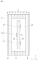
- FIG. 1 is an external perspective view of a multilayer substrate 100.
- FIG. 2 is a top view of each layer of the multilayer substrate 100 when viewed from the thickness direction.
- FIG. 3 is a cross-sectional view of the multilayer substrate 100 after deformation according to the first embodiment.
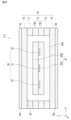
- 4 is a sectional view taken along line AA of the multilayer substrate 100
- FIG. 5 is a sectional view taken along line BB of the multilayer substrate 100.
- direction is defined as follows.
- the X-axis direction corresponds to the substrate stretching direction S of the multilayer substrate 100
- the Y-axis direction corresponds to the width direction W of the multilayer substrate 100
- the Z-axis direction corresponds to the thickness direction T of the multilayer substrate 100.
- the substrate stretching direction S is the direction in which the multilayer substrate 100 extends when viewed in the thickness direction T.
- the width direction W is a direction perpendicular to the direction in which the multilayer substrate 100 extends when viewed in the thickness direction T.
- the thickness direction T is the lamination direction in which at least one flexible resin layer 70 is laminated.
- the thickness direction T, the width direction W, and the substrate stretching direction S are orthogonal to each other. Note that the thickness direction T, width direction W, and substrate stretching direction S in this specification do not have to match the thickness direction, width direction, and signal transmission direction when the multilayer substrate 100 is actually used.
- a and B are electrically connected means that electricity can be conducted between A and B. Therefore, A and B may be in contact with each other, or A and B may not be in contact with each other. For example, when a conductive C is placed between A and B, A and B are electrically connected via C even if A and B are not in contact with each other.
- a and B are in contact means that A and B are connected in a contacting state.
- first and second are used only for descriptive purposes, and are not used to express or imply relative importance or ranking of technical features. Not to be understood.
- Features defined as “first” and “second” are expressly or implied to include one or more such features.
- the structure of the multilayer substrate 100 will be explained with reference to FIG. 1.
- the multilayer substrate 100 is a multilayer substrate for transmitting high frequency signals.
- the multilayer board 100 is, for example, a multilayer board for electrically connecting two circuits in an electronic device such as a smartphone.
- the multilayer substrate 100 has flexibility and can be bent as appropriate.
- the multilayer substrate 100 of the first embodiment has a shape extending in the substrate stretching direction S, as shown in FIG.
- the multilayer substrate 100 includes a laminate 10, a first inner layer resin 25, a plurality of conductors 30, and a conductive shield material 34.
- the laminate 10 has a plate shape with a first main surface 10a and a second main surface 10b separated in the thickness direction T. Specifically, the first main surface 10a and the second main surface 10b are opposed to each other.
- the first principal surface 10a may be referred to as an upper principal surface
- the second principal surface 10b may be referred to as a lower principal surface.
- a space 40 is provided inside the laminate 10.
- the laminate 10 has a plurality of laminated flexible resin layers 70, 71, 72, 73, and 74.
- the flexible resin layers 70, 71, 72, 73, and 74 are laminated along the thickness direction T. Specifically, the flexible resin layers 70, 71, 72, 73, and 74 are laminated in this order in the direction from the first main surface 10a to the second main surface 10b.
- the flexible resin layers 70, 71, 72, 73, and 74 have plate shapes with substantially the same dimensions. In this embodiment, in the thickness direction T, the outer surface of the flexible resin layer 70 forms the first main surface 10a, and the outer surface of the flexible resin layer 74 forms the second main surface 10b. are doing.
- the space 40 can be provided, for example, by removing a portion of the flexible resin layers 71, 72, and 73.
- the flexible resin layers 71, 72, and 73 are provided with holes that form the spaces 40.
- the flexible resin layers 71, 72, 73 are provided with, for example, rectangular holes.
- the flexible resin layers 70 and 74 are not provided with holes and have a continuous shape.
- the plurality of holes provided in the flexible resin layers 71, 72, 73 communicate in the thickness direction T.
- the flexible resin layers 71, 72, 73 are sandwiched between the flexible resin layers 70, 74 in the thickness direction T.
- the flexible resin layer 70 closes the hole openings in the flexible resin layer 71, and the flexible resin layer 74 closes the hole openings in the flexible resin layer 73.
- a space 40 formed by a plurality of consecutive holes is formed inside the laminate 10.
- the space 40 is formed into a rectangular shape when viewed in the thickness direction T. Air exists in the space 40.
- the flexible resin layers 70, 71, 72, 73, and 74 are, for example, flexible dielectric sheets.
- the material of the flexible resin layers 70, 71, 72, 73, and 74 is a thermoplastic resin.
- the thermoplastic resin include liquid crystal polymer, PTFE (polytetrafluoroethylene), and the like.
- the material of the flexible resin layers 70, 71, 72, 73, and 74 may be thermosetting resin or polyimide.
- the thermosetting resin is, for example, polyimide.
- the laminate 10 has an inner surface defining a space 40. More specifically, the laminate 10 includes a first inner wall 10A facing the first main surface 10a, a second inner wall 10B facing the second main surface 10b, and an inner wall 10S connecting them.
- the first inner wall 10A is defined by the flexible resin layer 70. Specifically, the first inner wall 10A is the inner surface of the flexible resin layer 70 on the side connected to the flexible resin layer 71. The first inner wall 10A is formed on the opposite side to the first main surface 10a formed on the flexible resin layer 71.
- the second inner wall 10B is defined by a flexible resin layer 74. Specifically, the second inner wall 10B is the inner surface of the flexible resin layer 74 on the side connected to the flexible resin layer 73. The second inner wall 10B is formed on the opposite side to the second main surface 10b formed on the flexible resin layer 74.
- the inner wall 10S is defined by flexible resin layers 71, 72, and 73. Specifically, the inner wall 10S is formed by a plurality of inner wall surfaces defining holes formed in the flexible resin layers 71, 72, and 73. Although the space 40 is defined by a plurality of inner walls in this embodiment, it may be defined by one inner wall. For example, a spherical inner wall can be mentioned.
- the first inner layer resin 25 is arranged in the space 40 of the laminate 10.
- the first inner layer resin 25 has a sheet shape extending in the substrate stretching direction S of the multilayer substrate 100.
- the first inner layer resin 25 has a third main surface 25a and a fourth main surface 25b that are separated in the thickness direction T.
- the first inner layer resin 25 is made of a flexible resin. Therefore, it can be bent by applying an external force. For example, when force is applied to the outside of the laminate 10, the first inner layer resin 25 deforms to curve within the space 40, as shown in FIG.
- the first inner layer resin 25 extends in the extending direction of the signal conductor 31 and is connected to the laminate 10 in the extending direction.
- the first inner layer resin 25 is connected to the laminate 10 in the substrate stretching direction S of the multilayer substrate 100.
- both ends of the first inner layer resin 25 in the substrate stretching direction S of the multilayer substrate 100 are connected to the inner wall 10S of the laminate 10.
- the first inner layer resin 25 is separated from the laminate 10 within the space 40. Specifically, in the cross section in the direction (Z direction) perpendicular to the direction in which the signal conductor 31 extends, the first inner layer resin 25 in the space 40 covers the first inner wall 10A, the second inner wall 10B, and the inner wall of the laminate 10. 10S and floating from the stacked body 10. That is, in a cross section in a direction (Z direction) perpendicular to the extending direction of the signal conductor 31, a hollow portion 40a is formed inside the laminate 10 to surround the first inner layer resin 25 in an annular shape. For example, the hollow portion 40a is filled with air.
- first inner layer resin 25 may be in contact with the laminate 10.
- a portion of the first inner layer resin 25 may be in contact with the laminate 10 when the multilayer substrate 100 is bent. That is, it is sufficient that at least a portion of the first inner layer resin 25 is separated from the laminate 10 within the space 40 .
- the first inner layer resin 25 is formed integrally with the flexible resin layer 72. Therefore, the first inner resin layer 25 is made of the same resin as the flexible resin layer 72. In other words, the first inner layer resin 25 is constituted by a part of the laminate 10.
- the first inner layer resin 25 may be formed of a separate member from the flexible resin layer 72, or may be formed of a different material from the flexible resin layer 72.
- the plurality of conductors 30 are conductor patterns provided on a portion of the laminate 10 and the first inner layer resin 25, and extend along the substrate stretching direction S. As shown in FIG. 4, the plurality of conductors 30 are provided on the third main surface 25a of the first inner resin layer 25. As shown in FIG.
- the plurality of conductors 30 may be provided on at least one of the third main surface 25a or the fourth main surface 25b of the first inner layer resin 25.
- the plurality of conductors 30 include a signal conductor 31 and a plurality of inner layer ground conductors 32.
- the plurality of conductors 30 are, for example, conductor layers formed by patterning metal foil pasted on the flexible resin layer 70.
- the metal foil is, for example, copper foil.
- the plurality of conductors may be formed by plating.
- the signal conductor 31 is a conductor for transmitting signals. In this embodiment, the signal conductor 31 transmits a high frequency signal.
- the signal conductor 31 is arranged with a gap between the two inner layer ground conductors 32.
- both ends of the signal conductor 31 in the substrate stretching direction S are arranged on a flexible resin layer 72 that defines the laminate 10. Specifically, both ends of the signal conductor 31 in the substrate stretching direction S are arranged in a portion of the flexible resin layer 72 on which the flexible resin layer 71 is laminated. Both ends of the signal conductor 31 in the substrate stretching direction S are connected to interlayer connection conductors 50a provided on the flexible resin layers 70 and 71.
- the interlayer connection conductor 50a is a conductor placed in a through hole provided in the thickness direction of the flexible resin layers 70 and 71.
- the interlayer connection conductor 50a is connected to a lead conductor 52a provided on the first main surface 10a of the flexible resin layer 70.
- the lead conductor 52a is arranged in the conductive shield material 34 arranged on the first main surface 10a of the laminate 10 and in the opening 46a provided in the protective film 11a.
- Each of the plurality of inner layer ground conductors 32 is a conductor connected to a ground potential. As shown in FIG. 2, the plurality of inner layer ground conductors 32 are arranged at intervals with the signal conductor 31 sandwiched therebetween. Both ends of the plurality of inner-layer ground conductors 32 in the substrate stretching direction S are arranged in the flexible resin layer 72 that defines the laminate 10, similarly to the signal conductor 31. Specifically, both ends of the plurality of inner layer ground conductors 32 in the substrate stretching direction S are arranged in the portion of the flexible resin layer 72 on which the flexible resin layer 71 is laminated. Both ends of the plurality of inner layer ground conductors 32 in the substrate stretching direction S are connected to interlayer connection conductors 50b provided on the flexible resin layer 71.
- the interlayer connection conductor 50b is a conductor placed in a through hole provided in the thickness direction of the flexible resin layers 70 and 71.
- the interlayer connection conductor 50b is connected to a lead-out conductor 52b provided on the flexible resin layer 70.
- the lead conductor 52b is arranged in the conductive shield material 34 arranged on the first main surface 10a of the laminate 10 and in the opening 46b provided in the protective film 11a.
- the conductive shield material 34 is provided on the first main surface 10a and the second main surface 10b of the laminate 10.
- the conductive shield material 34 is a film-like conductor that is provided on the flexible resin layers 70 and 74 and covers the main surfaces of the flexible resin layers 70 and 74 in the thickness direction, respectively. It's a pattern.
- the conductive shield material 34 is a conductive layer formed by patterning metal foil pasted on the flexible resin layers 70 and 74.
- the metal foil is, for example, copper foil.
- the conductive shield material 34 includes a first ground conductor 36 and a second ground conductor 38.
- the first ground conductor 36 is arranged on the first main surface 10a of the laminate 10.
- the second ground conductor 38 is arranged on the second main surface 10b of the laminate 10.
- the first ground conductor 36 and the second ground conductor 38 are each conductors connected to the ground potential.
- the first ground conductor 36 and the second ground conductor 38 have the role of suppressing the influence of noise from the outside world on the signal conductor 31, for example.
- Protective films 11a and 11b are arranged on the surface of the conductive shield material 34.
- the protective film 11a is, for example, a protective layer for protecting the first ground conductor 36 disposed on the first main surface 10a of the laminate 10.
- the protective film 11b is, for example, a protective layer for protecting the second ground conductor 38 disposed on the second main surface 10b of the laminate 10.
- the protective films 11a and 11b cover substantially the entire first main surface 10a and second main surface 10b of the stacked body 10, respectively.
- the protective films 11a and 11b are, for example, resin resists applied to the laminate 10. Note that the protective films 11a and 11b may be coverlays that are pasted on the laminate 10.
- the protective film 11a is provided with a plurality of openings 46a and 46b.
- the openings 46a and 46b are provided to connect the plurality of conductors 30 to the outside.
- lead conductors 52a and 52b electrically connected to the plurality of conductors 30 are arranged in the plurality of openings 46a and 46b.
- the first inner layer resin 25 overlaps the space 40 when viewed from the thickness direction T.
- the space 40 is provided at a position sandwiching the first inner layer resin 25 in the thickness direction T and in the width direction W.
- the first inner layer resin 25 is spaced apart from the inner surface of the laminate 10 in the thickness direction and in the width direction W. Specifically, the first inner layer resin 25 is separated from the first inner wall 10A and the second inner wall 10B in the thickness direction T. Further, the first inner layer resin 25 is separated from the inner wall 10S in the width direction W, but is connected to the inner wall 10S in the substrate stretching direction S.
- the plurality of conductors 30 are arranged to face the first ground conductor 36 and the second ground conductor 38 when viewed from the thickness direction T.
- the multilayer substrate 100 it is possible to suppress fluctuations in the clearance between the plurality of conductors 30 due to deformation of the multilayer substrate 100.
- the outer portion of the laminate 10 is curved and deformed, as shown in FIG.
- the plurality of conductors 30 are not arranged in the first inner layer resin 25 and only the conductor pattern is arranged in the space 40, there is a possibility that the degree of deformation of the plurality of conductors 30 will be different. In that case, it is conceivable that the clearance between the plurality of conductors 30 will vary and the signal characteristics will deteriorate.
- the multilayer substrate 100 includes a laminate 10, a first inner layer resin 25, and a plurality of conductors 30.
- the laminate 10 has a plurality of laminated flexible resin layers 70 to 74, and has a space 40 provided therein.
- the first inner layer resin 25 is arranged in the space 40 of the laminate 10 .
- the plurality of conductors 30 include signal conductors and are arranged in the first inner layer resin 25. With such a configuration, the plurality of conductors 30 deform along with the deformation of the first inner layer resin 25, so that the plurality of conductors 30 can easily undergo similar deformation. This makes it difficult for differences in deformation to occur between the plurality of conductors 30. As a result, even if the multilayer substrate 100 is deformed, fluctuations in the clearance between the plurality of conductors 30 can be suppressed.
- the signal conductor 31 is for high frequency signals, and high frequency signals are transmitted. This can be expected to suppress deterioration of signal characteristics by suppressing changes in clearance with the inner layer ground conductor 32. Note that a signal different from the high frequency signal, such as a low frequency signal, may be transmitted to the signal conductor 31.
- interlayer connection conductors 50a, 50b and lead-out conductors 52a, 52b are provided in flexible resin layers 70, 71 on one side and the other side of the laminate 10 in the substrate stretching direction S. did.
- the lead conductors 52a and 52b are arranged in the conductive shield material 34 arranged on the first main surface 10a of the laminate 10 and in the openings 46a and 46b provided in the protective film 11a.
- the interlayer connection conductors 50a, 50b and the lead-out conductors 52a, 52b may be provided in the flexible resin layers 73, 74 on at least one of one side or the other side of the laminate 10 in the substrate stretching direction S.
- openings 46a and 46b may be provided in the conductive shield material 34 and the protective film 11a disposed on the second main surface 10b of the laminate 10.
- the lead conductors 52a and 52b may be arranged in the conductive shield material 34 and the openings 46a and 46b provided in the protective film 11a, which are arranged on the second main surface 10b of the laminate 10.
- FIG. 6 is a longitudinal cross-sectional view of the multilayer substrate 101 according to the first modification.
- the multilayer substrate 101 according to the first modification differs from the multilayer substrate 100 according to the first embodiment in that it does not include the first ground conductor 36 and the second ground conductor 38.
- the multilayer substrate 101 has a structure in which protective films 11a and 11b are laminated on the laminate 10 in the thickness direction T. Specifically, a protective film 11a is laminated on the first main surface 10a of the laminate 10, and a protective film 11b is laminated on the second main surface 10b.
- FIG. 7 is a longitudinal cross-sectional view of a multilayer substrate 102 according to a second modification.
- the multilayer substrate 102 according to the second modification differs from the multilayer substrate 100 according to the first embodiment in the configuration of the plurality of conductors 30.
- the plurality of conductors 30 include one signal conductor 31 and one inner layer ground conductor 32.
- the configuration of the plurality of conductors 30 is not limited to the configurations of the first embodiment and the second modification.
- the plurality of conductors 30 may have any configuration as long as the characteristics are affected by the clearance between the plurality of conductors 30.
- the plurality of conductors 30 may have two signal conductors 31, and the two signal conductors 31 may constitute a differential line. Furthermore, two inner layer ground conductors 32 may be placed at positions sandwiching the differential line therebetween.
- FIG. 8 is a partially enlarged view of the multilayer substrate 103 according to the second embodiment.
- FIG. 8 shows an enlarged view of a part of the first inner resin layer 25 provided with a plurality of conductors 30. As shown in FIG.
- the multilayer substrate 103 according to the second embodiment is different from the multilayer substrate 100 according to the first embodiment in the width of the signal conductor 31 and the width of the inner layer ground conductor 32.
- the signal conductor 31 has a first portion 41 and a second portion 42.
- the width of the first portion 41 is larger than the width of the second portion 42 when viewed from the thickness direction T.
- two second portions 42 are connected to both ends of the first portion 41. That is, the first portion 41 is sandwiched between the two second portions 42.
- the first portion 41 is located in the space 40 of the laminate 10. Specifically, the first portion 41 is located in the first region R1 in which the space 40 is formed within the laminate 10 when viewed from the thickness direction T of the laminate 10.
- the first region R1 is a region defined by the inner wall 10S of the laminate 10 when viewed from the thickness direction T.
- the second portion 42 is not located in the space 40 within the laminate 10.
- the second portion 42 is located in a second region R2 in the laminate 10 in which the space 40 is not formed, when viewed from the thickness direction T of the laminate 10.
- the second region R2 is a region located outside the first region R1 when viewed from the thickness direction T, and is a region where the flexible resin layer 72 is arranged.
- the second region R2 is disposed outside the first region R1 in the substrate stretching direction S when viewed in the thickness direction T. Therefore, the second portion 42 extends from the inside of the laminate 10 toward the space 40 and is connected to the first portion 41 when viewed from the thickness direction T.
- the width of the first portion 41 is 1.1 times or more and 3.0 times or less than the width of the second portion 42.
- the width of the first portion 41 may be the maximum dimension in the width direction W when viewed from the thickness direction T.
- the width of the second portion 42 may be the minimum dimension in the width direction W when viewed from the thickness direction T.
- the inner layer ground conductor 32 has a third portion 43 and a fourth portion 44 that is wider than the third portion 43.
- two fourth portions 44 are connected to both ends of the third portion 43. That is, the third portion 43 is sandwiched between the two fourth portions 44.
- the third portion 43 is located in the space 40 within the laminate 10. Similar to the first portion 41, the third portion 43 is located in the first region R1 when viewed from the thickness direction T of the laminate 10.
- the fourth portion 44 is not located in the space 40 within the laminate 10. Similar to the second portion 42, the fourth portion 44 is located in the second region R2 when viewed from the thickness direction T of the laminate 10. Therefore, the fourth portion 44 extends from the inside of the laminate 10 toward the space 40 and is connected to the third portion 43 when viewed from the thickness direction T.
- the multilayer substrate 103 can be made smaller.
- the width of the fourth portion 44 of the inner layer ground conductor 32 may be larger than the width of the second portion 42 of the signal conductor 31.
- the width of the second portion 42 and the width of the fourth portion 44 refer to dimensions in the width direction W when viewed from the thickness direction T.
- the present invention is not limited to this.
- the width of the inner layer ground conductor 32 may be constant.
- FIG. 9 is a longitudinal cross-sectional view of the multilayer substrate 104 according to the third embodiment.
- the multilayer substrate 104 according to the third embodiment differs from the multilayer substrate 100 according to the first embodiment in the configuration of the laminate 10 and the position of the first inner layer resin 25.
- the laminate 10 further includes a flexible resin layer 75.
- Flexible resin layer 75 is arranged between flexible resin layers 73 and 74.
- the flexible resin layer 75 has the same shape as the flexible resin layer 73, for example.
- the first inner layer resin 25 is unevenly distributed with respect to the multilayer substrate 104 in the thickness direction T of the multilayer substrate 104.
- the first inner resin layer 25 is located closer to the flexible resin layer 70 than the flexible resin layer 74 .
- the first inner layer resin 25 is disposed at a position closer to the first main surface 10a of the laminate 10 than the second main surface 10b in the thickness direction T.
- the distance between the first inner wall 10A of the laminate and the third main surface 25a of the first inner layer resin 25 is the same as the distance between the second inner wall 10B of the laminate 10 and the fourth main surface of the first inner layer resin 25. It is smaller than the distance from the surface 25b.
- the bending stress of the first inner layer resin 25 depends on the distance from the bending neutral line.
- compressive stress is generated on the inner circumferential side of the bent portion, and tensile stress is generated on the outer circumferential side of the bent portion.
- the compressive stress and the tensile stress become smaller toward the inner center in the thickness direction of the first inner layer resin 25, and there is a position where the compressive stress and the tensile stress become zero. This position is called the bending neutral line.
- the bending neutral line When the distance from this bending neutral line is zero, the bending stress is zero, and the farther the distance is, the larger the bending stress becomes. Since the first inner layer resin 25 is located away from the laminate 10 within the space 40, the bending stress can be reduced even if the first inner layer resin 25 is located away from the bending neutral line.
- the first inner layer resin 25 is unevenly distributed in the thickness direction T by adding one flexible resin layer 75 to the laminate 10, but the present invention is not limited to this.
- the first inner layer resin 25 may be unevenly distributed in the thickness direction T by increasing the thickness of the flexible resin layer 73.
- the first inner layer resin 25 may be unevenly distributed in the thickness direction T by adding one or more flexible resin layers 75.
- the flexible resin layer 75 has the same shape as the flexible resin layer 73 has been described, but the present invention is not limited to this.
- the flexible resin layer 75 may have a different shape and thickness from the flexible resin layer 73.
- the first inner layer resin 25 is arranged at a position closer to the flexible resin layer 70 than the flexible resin layer 74 in the thickness direction T, but the present invention is not limited to this.
- the first inner resin layer 25 may be placed closer to the flexible resin layer 74 than the flexible resin layer 70 in the thickness direction T.
- FIG. 10 is a longitudinal cross-sectional view of a multilayer substrate 105 according to the fourth embodiment.
- the multilayer substrate 105 according to the fourth embodiment is different from the multilayer substrate 100 according to the first embodiment in the configuration of the laminate 10 and in that it further includes a plurality of second inner layer resins 26.
- the laminate 10 further includes flexible resin layers 77, 78, 79, and 80.
- Flexible resin layers 77 and 78 are arranged between flexible resin layers 71 and 72.
- Flexible resin layers 79 and 80 are arranged between flexible resin layers 72 and 73.
- the flexible resin layers 77 and 80 have the same shape as the flexible resin layer 72, for example.
- the flexible resin layers 78 and 79 have the same shape as the flexible resin layer 71, for example.
- the multilayer substrate 105 further includes a plurality of second inner layer resins 26.
- the plurality of second inner layer resins 26 have the same shape as the first inner layer resin 25, for example.
- the plurality of second inner layer resins 26 are arranged in the space 40 of the laminate 10. Specifically, in the space 40 of the laminate 10, a plurality of second inner layer resins 26 are arranged at intervals in the thickness direction T of the laminate 10.
- the first inner layer resin 25 is arranged between the plurality of second inner layer resins 26 in the thickness direction T. More specifically, the plurality of second inner layer resins 26 are located between the third main surface 25a of the first inner layer resin 25 and the first inner wall 10A of the laminate 10, and between the fourth main surface of the first inner layer resin 25. 25b and the second inner wall 10B of the laminate 10.
- the plurality of second inner layer resins 26 are each formed integrally with the flexible resin layers 77 and 80. Therefore, the plurality of second inner resin layers 26 are made of the same resin as the flexible resin layers 77 and 80. In other words, the plurality of second inner layer resins 26 are constituted by a part of the laminate 10.
- the plurality of second inner layer resins 26 are connected to the laminate 10 in the substrate stretching direction S of the multilayer substrate 100. Specifically, the plurality of second inner layer resins 26 are separated from the first inner wall 10A and the second inner wall 10B in the thickness direction T. The plurality of second inner layer resins 26 are separated from the inner wall 10S in the width direction W, while being connected to the inner wall 10S in the substrate stretching direction S.
- the multilayer board 105 since the multilayer board 105 includes the plurality of second inner layer resins 26, the first inner layer resin 25 and the plurality of conductors 30 come close to the first ground conductor 36 and the second ground conductor 38. suppress things. For example, when the multilayer substrate 105 is deformed, the first inner layer resin 25 comes into contact with the second inner layer resin 26, so the distance between the plurality of conductors 30 and the first ground conductor 36 and the second ground conductor becomes smaller. can be suppressed. Thereby, fluctuations in impedance of the plurality of conductors 30 can be suppressed.
- the multilayer substrate 105 may include one or more second inner layer resins 26.
- the multilayer substrate 105 may be arranged in a space 40 that becomes a mountain fold side with respect to the first inner layer resin 25 when the multilayer substrate 105 is bent. .
- FIG. 11A is a vertical cross-sectional view of the multilayer substrate 106 according to the fifth embodiment.
- FIG. 11B is a partially enlarged view showing an example of the plurality of first through holes 60 provided in the laminate 10.
- the multilayer substrate 106 according to the fifth embodiment is different from the multilayer substrate 105 according to the fourth embodiment in the structures of the flexible resin layers 70A to 78A, the first inner layer resin 25A, and the second inner layer resin 26A.
- a plurality of first through holes 60 are provided throughout the laminate 10, the first inner layer resin 25A, and the second inner layer resin 26A.
- the laminate 10 has flexible resin layers 70A to 74A and flexible resin layers 77A to 80A.
- the flexible resin layers 70A to 74A and the flexible resin layers 77A to 80A are different from each other, except that the plurality of first through holes 60 are provided.
- Each of the layers 77 to 80 has a similar shape.
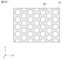
- the plurality of first through holes 60 are regularly provided holes. Specifically, the plurality of first through holes 60 have substantially the same shape and size, and are provided at equal intervals. For example, the plurality of first through holes 60 are provided in a matrix when viewed from the thickness direction T.
- the shape of the plurality of first through holes 60 has, for example, a circular shape when viewed from the thickness direction T.
- the plurality of first through holes 60 have an opening width of, for example, 81 ⁇ m or more and 500 ⁇ m or less.
- the "opening width" refers to the maximum dimension of the first through hole 60.
- the opening width means the maximum diameter of the first through hole 60 when viewed from the thickness direction T.
- the distance between the plurality of first through holes 60 is, for example, 73 ⁇ m or more and 730 ⁇ m or less.
- the flexible resin layers 70A to 74A, the flexible resin layers 77A to 80A, the first inner resin layer 25A, and the second inner resin layer 26A are each made of, for example, a mesh member.
- the plurality of first through holes 60 are provided using, for example, a laser.
- the plurality of first through holes 60 are not holes of interlayer connection conductors such as via conductors. Therefore, air exists inside the first through hole 60.
- the amount of resin included in the multilayer substrate 106 is reduced. This makes the multilayer substrate 106 easier to bend, improving usability.
- a plurality of first through holes 60 may be provided in at least a portion of the laminate 10, the first inner layer resin 25A, or the second inner layer resin 26A.
- the plurality of first through holes 60 may be provided in some parts of the flexible resin layers 70A, 74A of the laminate 10, and the plurality of first through holes 60 may not be provided in other parts. Good too.
- a plurality of first through holes 60 may be provided in a part of the first inner layer resin 25A or the second inner layer resin 26A.
- a plurality of first through holes 60 may be provided at positions overlapping with the signal conductors 31 when viewed in the thickness direction T of the laminate 10. This reduces the dielectric constant and dielectric loss tangent around the signal conductor 31, and improves electrical characteristics.
- the shape of the plurality of first through holes 60 is not limited, and may be, for example, a triangular pyramid shape. Furthermore, the shape when viewed from the thickness direction T is not limited, and may be, for example, an ellipse.
- a plurality of first through holes 60 are provided throughout A of the flexible resin layers 70A to 74A, the flexible resin layers 77A to 80A, the first inner layer resin 25A, and the second inner layer resin 26. Not limited. Further, it is limited that the plurality of first through holes 60 are provided in each of the flexible resin layers 70A to 74A, the flexible resin layers 77A to 80A, the first inner layer resin 25A, and the second inner layer resin 26A. do not.
- the plurality of first through holes 60 do not have to be arranged regularly.
- the plurality of first through holes 60 may be provided randomly.
- the sizes or shapes of the plurality of first through holes 60 may be different.
- the second inner layer resin 26A is not an essential component.
- FIG. 11C is a partially enlarged cross-sectional view showing an example of a porous material.
- the multilayer substrate according to the modification of the fifth embodiment is different from the multilayer substrate 106 according to the fifth embodiment in that the laminate 10, the first inner layer resin 25A, and the second inner layer resin 26A are made of porous materials. differ.
- a porous material is a material that has a porous structure.
- the porous structure is a structure in which a plurality of air bubbles P are dispersed throughout the porous region A.
- the porous region A means a region in which a plurality of air bubbles P are provided in the element body 12 constituting the porous material.
- the porous region A is provided throughout the laminate 10, the first inner layer resin 25A, and the second inner layer resin 26A.
- the porous region A contains a plurality of closed cells.
- the closed cell has a structure in which the entire bubble P is surrounded by the material of the element body 12, so that the gas inside the bubble P cannot leak to the outside of the element body 12. Furthermore, in closed cells, adjacent cells P are not connected to each other.
- the porosity of the porous region A is, for example, 30% or more and 80% or less. The porosity is the ratio of the volume of the bubbles P to the entire volume of the element body 12.
- the present invention is not limited thereto.
- at least a portion of the laminate 10, the first inner layer resin 25A, or the second inner layer resin 26A may be made of a porous material.
- the porous region A may also be provided in at least a portion of the laminate 10, the first inner layer resin 25A, or the second inner layer resin 26A.
- FIG. 11D is a partially enlarged sectional view showing another example of the porous material. As shown in FIG. 11D, a plurality of bubbles Q may be connected and provided in the porous material. Moreover, the shapes and/or sizes of the plurality of bubbles Q may be different.
- FIG. 12A is a vertical cross-sectional view of the multilayer substrate 107 according to the sixth embodiment.
- FIG. 12B is a partially enlarged view showing an example of the plurality of second through holes 53 provided in the second inner layer resin 26B.
- the multilayer substrate 107 according to the sixth embodiment differs from the multilayer substrate 105 according to the fourth embodiment in the structure of the second inner layer resin 26B.
- a plurality of second through holes 53 are provided in the second inner layer resin 26B.
- a plurality of second through holes 53 are provided in each of the two second inner layer resins 26B.
- the plurality of second through holes 53 are provided at positions overlapping with the signal conductor 31 when viewed in the thickness direction T.
- the plurality of second through holes 53 are provided along the direction in which the signal conductor 31 extends, that is, the substrate extension direction S when viewed in the thickness direction T.
- the plurality of second through holes 53 have, for example, a circular shape when viewed in the thickness direction T.
- the length of the second through hole 53 in the width direction W is longer than the length of the signal conductor 31 in the width direction W.
- the second through hole 53 has an opening width of, for example, 1/6 or more and 1/3 or less of the length in the width direction W of the laminate 10.
- the "opening width” refers to the maximum dimension of the second through hole 53 in the width direction W of the laminate 10.
- the opening width means the maximum diameter of the second through hole 53.
- the portion where the second inner layer resin 26B is arranged in the region overlapping with the signal conductor 31 when seen in the thickness direction T can be reduced. Air having a lower dielectric constant than the second inner layer resin 26B exists in the plurality of second through holes 53. Therefore, the signal characteristics of the signal conductor 31 can be improved.
- the length of the second through hole 53 in the width direction W is longer than the length of the signal conductor 31 in the width direction W. With this configuration, the signal characteristics of the signal conductor 31 can be further improved.
- the multilayer substrate 107 includes two second inner layer resins 26B has been described, but the present invention is not limited to this.
- the multilayer substrate 107 may include one or more second inner layer resins 26B.
- second through holes 53 are provided in the second inner layer resin 26B
- the present invention is not limited to this.
- one or more second through holes 53 may be provided in the second inner layer resin 26B.
- one rectangular second through hole 53 may be provided in the second inner layer resin 26B.
- a plurality of second through holes 53 are provided in both of the two second inner layer resins 26B, but the present invention is not limited to this.
- a plurality of second through holes 53 may be provided in at least one of the two second inner layer resins 26B.
- the shape of the second through hole 53 is not limited, and may be, for example, triangular pyramid shape. Further, the shape of the second through hole 53 when viewed from the thickness direction T is not limited, and may be, for example, an ellipse, a rectangle, or a polygon.
- FIG. 13A is a vertical cross-sectional view of the multilayer substrate 108 according to the seventh embodiment.
- FIG. 13B is a partially enlarged view showing an example of the plurality of third through holes 54 provided in the flexible resin layer 70.
- the multilayer substrate 108 according to the seventh embodiment is different from the multilayer substrate 107 according to the sixth embodiment in the structure of the laminate 10.
- a plurality of third through holes 54 are further provided in the flexible resin layers 70 and 74.
- the plurality of third through holes 54 are provided at positions overlapping with the signal conductor 31 when viewed in the thickness direction T. Further, the plurality of third through holes 54 are provided along the direction in which the signal conductor 31 extends, that is, the substrate extension direction S when viewed in the thickness direction T.
- the plurality of third through holes 54 have, for example, a circular shape when viewed in the thickness direction T.
- the length of the through hole 54 in the width direction W is longer than the length of the signal conductor 31 in the width direction W.
- the third through hole 54 has an opening width that is, for example, 1/6 or more and 1/3 or less of the length in the width direction W of the laminate 10.
- the "opening width” refers to the maximum dimension of the third through hole 54 in the width direction W of the laminate 10.
- the opening width means the maximum diameter of the third through hole 54.
- the plurality of third through holes 54 are provided at positions overlapping with the plurality of through holes 53 provided in the second inner layer resin 26B when viewed in the thickness direction T.
- the plurality of third through holes 54 have the same shape, size, and arrangement as the plurality of through holes 53.
- the flexible resin layer 70 by providing the plurality of third through holes 54 in the flexible resin layers 70, 74, the flexible resin layer 70, The portion where 74 is arranged can be reduced. Air having a lower dielectric constant than the flexible resin layers 70 and 74 exists in the plurality of third through holes 54 . Therefore, in the multilayer substrate 108, the signal characteristics of the signal conductor 31 can be improved.
- the plurality of third through holes 54 are provided at positions overlapping with the plurality of through holes 53 provided in the second inner layer resin 26B. With such a configuration, the signal characteristics of the signal conductor 31 can be further improved.
- the length of the through hole 54 in the width direction W is longer than the length of the signal conductor 31 in the width direction W. As a result, the dielectric constant around the signal conductor 31 is reduced, so that the signal characteristics of the signal conductor 31 can be improved.
- a plurality of through holes 54 are provided in the flexible resin layers 70 and 74 , but the present invention is not limited to this.
- a plurality of third through holes 54 may be provided in at least one of the flexible resin layer 70 or 74.
- one or more third through holes 54 may be provided in the flexible resin layer 70 or 74.
- one rectangular third through hole 54 may be provided in the flexible resin layer 70 or 74.
- the plurality of third through holes 54 may have a shape, size, and arrangement different from those of the plurality of through holes 53.
- the shape of the through hole 54 is not limited, and may be, for example, triangular pyramid shape. Further, the shape of the third through hole 54 when viewed from the thickness direction T is not limited, and may be, for example, elliptical, rectangular, or polygonal.
- FIG. 14A is a vertical cross-sectional view of the multilayer substrate 109 according to the eighth embodiment.
- FIG. 14B is a partially enlarged view showing an example of the plurality of first protrusions 27 provided on the first inner layer resin 25.
- FIG. 14A is a vertical cross-sectional view of the multilayer substrate 109 according to the eighth embodiment.
- FIG. 14B is a partially enlarged view showing an example of the plurality of first protrusions 27 provided on the first inner layer resin 25.
- the multilayer substrate 109 according to the eighth embodiment is different from the multilayer substrate 100 according to the first embodiment in the configuration of the laminate 10 and in that it further includes a plurality of first protrusions 27.
- the laminate 10 further includes flexible resin layers 78 and 79.
- Flexible resin layer 78 is arranged between flexible resin layers 71 and 72
- flexible resin layer 79 is arranged between flexible resin layers 72 and 73.
- the flexible resin layers 78 and 79 have the same shape as the flexible resin layer 73, for example.
- the multilayer substrate 109 further includes a first protrusion 27.
- the first inner layer resin 25 has a plurality of first protrusions 27 that protrude in the thickness direction T of the laminate 10 . More specifically, the plurality of first protrusions 27 are provided on both the third main surface 25a and the fourth main surface 25b of the first inner layer resin 25 in the thickness direction T. The plurality of first protrusions 27 are formed with substantially the same shape and dimensions.
- each of the plurality of first protrusions 27 has a rectangular parallelepiped shape.
- the plurality of first protrusions 27 are arranged on the outer side of the plurality of conductors 30 when viewed in the thickness direction T. Specifically, when viewed in the thickness direction T, the plurality of first protrusions 27 are arranged on both outer sides of the plurality of conductors 30 in the width direction W in which the plurality of conductors 30 are lined up.
- the height of the plurality of first protrusions 27 in the thickness direction T is greater than the thickness of the plurality of conductors 30 in the thickness direction T. Further, the height of the plurality of first protrusions 27 in the thickness direction T is smaller than the distance between the first inner wall 10A of the laminate 10 and the third main surface 25a of the first inner layer resin 25 in the thickness direction T.
- the plurality of first protrusions 27 provided on the fourth main surface 25b of the first inner layer resin 25 are provided at positions overlapping with the plurality of first protrusions 27 provided on the third main surface 25a when viewed in the thickness direction T. There is. Further, on the fourth main surface 25b of the first inner layer resin 25, the height of the plurality of first protrusions 27 in the thickness direction T is the same as that of the second inner wall 10B of the laminate 10 in the thickness direction T. It is smaller than the distance between the four main surfaces 25b.
- the plurality of first protrusions 27 are located outside the two inner layer ground conductors 32. Specifically, when viewed in the thickness direction T, the plurality of first protrusions 27 are arranged between the end of the first inner layer resin 25 and the inner layer ground conductor 32 in the width direction W. The plurality of first protrusions 27 are arranged at intervals along the substrate stretching direction S. For example, the plurality of first protrusions 27 are arranged at equal intervals along the substrate stretching direction S.
- the multilayer substrate 109 includes the plurality of first protrusions 27, the first inner layer resin 25 and the plurality of conductors 30 do not approach the first ground conductor 36 and the second ground conductor 38. can be suppressed. Thereby, fluctuations in the impedance of the signal conductor 31 can be suppressed.
- the first inner layer resin 25 may be provided with one or more first protrusions 27 .
- one or more first protrusions 27 may be provided on the third main surface 25a or the fourth main surface 25b of the first inner layer resin 25.
- the plurality of first protrusions 27 may not be provided on both the third main surface 25a and the fourth main surface 25b of the first inner layer resin 25 in the thickness direction T.
- the plurality of first protrusions 27 may be provided on at least one of the third main surface 25a and the fourth main surface 25b of the first inner layer resin 25.
- it may be provided at least on the surface that becomes the mountain fold side when the multilayer substrate 109 is bent.
- the shape of the first protrusion 27 is not limited, and may be, for example, cylindrical or triangular pyramidal. Further, the shape of the cross section of the first protrusion 27 is not limited either.
- the first protrusion 27 may be placed outside the plurality of conductors 30.
- the first protrusion 27 may be arranged between the plurality of conductors 30.
- the width of the first protrusion 27 provided on the third main surface 25a of the first inner layer resin 25 is smaller than the interval between the plurality of conductors 30.
- the distance between the first protrusion 27 and the signal conductor 31 in the width direction W may be shorter than the distance between the inner layer ground conductor 32 and the signal conductor 31.
- the first protrusion 27 is closer to the signal conductor 31 than the inner layer ground conductor 32, so that fluctuations in impedance can be further suppressed.
- first protrusions 27 are arranged at equal intervals along the substrate stretching direction S, but the present invention is not limited to this.
- one continuous first protrusion 27 may be arranged along the substrate stretching direction S.
- the plurality of first protrusions 27 are formed with substantially the same shape and the same dimensions, but the present invention is not limited to this.
- the plurality of first protrusions 27 may be formed with different shapes or dimensions.
- FIG. 15A is a vertical cross-sectional view of the multilayer substrate 110 according to the ninth embodiment.
- FIG. 15B is a partially enlarged view showing an example of the plurality of second protrusions 28 provided on the second inner layer resin 26.
- the multilayer substrate 110 according to the ninth embodiment is different from the multilayer substrate 105 according to the fourth embodiment in the configuration of the laminate 10 and in that it further includes a plurality of second protrusions 28.
- the laminate 10 further includes flexible resin layers 81 and 82.
- Flexible resin layer 81 is arranged between flexible resin layers 71 and 77.
- Flexible resin layer 82 is arranged between flexible resin layers 80 and 73.
- the flexible resin layers 81 and 82 have the same shape as the flexible resin layer 73, for example.
- the multilayer substrate 110 further includes a plurality of second protrusions 28.
- the second inner layer resin 26 has a plurality of second protrusions 28 that protrude in the thickness direction T of the laminate 10.
- the plurality of second protrusions 28 are formed with substantially the same shape and the same dimensions.
- the plurality of second protrusions 28 are arranged at positions that do not overlap the signal conductors 31 when viewed in the thickness direction T.
- the plurality of second protrusions 28 are located between the inner layer ground conductor 32 and the conductive shield material 34.
- the plurality of second protrusions 28 are arranged at positions overlapping with the inner layer ground conductor 32 when viewed in the thickness direction T.
- the plurality of second protrusions 28 are arranged at intervals along the substrate stretching direction S.
- the plurality of second protrusions 28 are arranged at equal intervals along the substrate stretching direction S when viewed in the thickness direction T.
- each of the plurality of second protrusions 28 has a rectangular parallelepiped shape.
- the height of the plurality of second projections 28 in the thickness direction T is equal to the first inner wall 10A of the laminate 10. It is smaller than the distance between the second inner layer resin 26 and the second inner layer resin 26 .
- the height of the plurality of second protrusions 28 in the thickness direction T is determined by the second inner wall of the laminate 10. It is smaller than the distance between 10B and the second inner layer resin 26.
- the multilayer board 110 since the multilayer board 110 includes the plurality of second protrusions 28, the first inner layer resin 25 and the plurality of conductors 30 do not come close to the first ground conductor 36 or the second ground conductor 38. can be suppressed. Thereby, fluctuations in the impedance of the signal conductor 31 can be suppressed.
- the plurality of second protrusions 28 are arranged at positions that do not overlap with the signal conductor 31 when viewed in the thickness direction T. With such a configuration, the dielectric constant and dielectric loss tangent around the signal conductor 31 are reduced, and the electrical characteristics are improved.
- a plurality of second protrusions 28 are provided on each of the two second inner layer resins 26 , but the present invention is not limited to this.
- a plurality of second protrusions 28 may be provided on at least one second inner layer resin 26.
- a plurality of second protrusions 28 may be provided on the surface of the second inner layer resin 26 that becomes the mountain fold side when the multilayer substrate 110 is bent.
- the shape of the second protrusion 28 is not limited, and may be, for example, cylindrical or triangular pyramidal. Further, the cross-sectional shape of the second protrusion 28 is not limited either.
- the plurality of second protrusions 28 are provided at positions overlapping with the inner layer ground conductor 32 when viewed in the thickness direction T, but the present invention is not limited to this.
- the plurality of second protrusions 28 may be provided at positions that do not overlap the inner layer ground conductor 32 when viewed in the thickness direction T.
- the second inner layer resin 26 is provided with a plurality of second protrusions 28 , but the present invention is not limited to this.
- the second inner layer resin 26 may be provided with one or more second protrusions 28 .
- the plurality of second protrusions 28 are formed with substantially the same shape and the same dimensions, but the present invention is not limited to this.
- the plurality of second protrusions 28 may be formed with different shapes or dimensions.
- FIG. 16 is a longitudinal cross-sectional view of the multilayer substrate 111 according to the tenth embodiment.
- FIG. 17 is an exploded top view of the multilayer substrate 111 according to the tenth embodiment.
- FIG. 18 is a cross-sectional view of the multilayer substrate 111 after deformation according to the tenth embodiment.
- the multilayer substrate 111 according to the tenth embodiment is different from the multilayer substrate 100 according to the first embodiment in the configuration of the laminate 10 and in that it further includes a plurality of third protrusions 29.
- the laminate 10 further includes flexible resin layers 83 and 84.
- the flexible resin layer 83 is arranged between the flexible resin layers 70 and 71.
- Flexible resin layer 84 is arranged between flexible resin layers 73 and 74.
- the flexible resin layers 83 and 84 have the same shape as the flexible resin layer 73, for example.
- the multilayer substrate 111 further includes a plurality of third protrusions 29.
- the multilayer substrate 111 has a plurality of third protrusions 29 that protrude in the thickness direction T of the laminate 10 .
- the plurality of third protrusions 29 are provided on the inner surface of the laminate 10.
- the plurality of third protrusions 29 are provided on the first inner wall 10A and the second inner wall 10B of the stacked body 10.
- the plurality of third protrusions 29 provided on the first inner wall 10A of the laminate 10 protrude from the first inner wall 10A toward the third main surface 25a of the first inner layer resin 25 in the thickness direction T.
- the plurality of third protrusions 29 provided on the second inner wall 10B of the laminate 10 protrude from the second inner wall 10B toward the fourth main surface 25b of the first inner layer resin 25.
- the plurality of third protrusions 29 are arranged at positions that do not overlap with the signal conductors 31 when viewed in the thickness direction T.
- the plurality of third protrusions 29 are located between the inner layer ground conductor 32 and the conductive shield material 34.
- the plurality of third protrusions 29 are arranged at positions overlapping with the inner layer ground conductor 32 when viewed in the thickness direction T.
- the plurality of third protrusions 29 are arranged at intervals along the substrate stretching direction S.
- the plurality of third protrusions 29 are arranged at equal intervals along the substrate stretching direction S.
- the plurality of third protrusions 29 are formed with substantially the same shape and the same dimensions.
- each of the plurality of third protrusions 29 has a rectangular parallelepiped shape.
- the height of the plurality of third protrusions 29 in the thickness direction T is smaller than the distance between the inner surface of the laminate 10 and the first inner layer resin 25 in the thickness direction T.
- the height of the plurality of third protrusions 29 provided on the first inner wall 10A of the laminate 10 is smaller than the distance between the first inner wall 10A and the third main surface 25a of the first inner layer resin 25.
- the plurality of third protrusions 29 provided on the second inner wall 10B of the laminate 10 are smaller than the distance between the second inner wall 10B and the fourth main surface 25b of the first inner layer resin 25.
- the outer portion of the laminate 10 is curved and deformed.
- the first inner layer resin 25 and the plurality of conductors 30 deform.
- the plurality of third protrusions 29 protruding from the inner surface of the laminate 10 prevent the first inner layer resin 25 and the plurality of conductors 30 from approaching the first ground conductor 36 and the second ground conductor 38.
- the first inner layer resin 25 comes into contact with the plurality of third protrusions 29, thereby maintaining a state separated from the first ground conductor 36 and the second ground conductor 38.
- the multilayer substrate 111 includes the plurality of third protrusions 29, the first inner layer resin 25 and the plurality of conductors 30 do not approach the first ground conductor 36 and the second ground conductor 38. can be suppressed. Thereby, fluctuations in the impedance of the signal conductor 31 can be suppressed.
- the plurality of third protrusions 29 are arranged at positions that do not overlap with the signal conductor 31 when viewed in the thickness direction T. With such a configuration, the dielectric constant and dielectric loss tangent around the signal conductor 31 are reduced, and the electrical characteristics are improved.
- third protrusions 29 are provided on the inner surface of the laminate 10
- the present invention is not limited to this.
- one or more third protrusions 29 may be provided on the inner surface of the laminate 10.
- a plurality of third protrusions 29 are provided on both the first inner wall 10A and the second inner wall 10B of the laminate 10, but the present invention is not limited to this.
- the plurality of third protrusions 29 may be provided on at least one of the first inner wall 10A and the second inner wall 10B.
- it may be provided on the inner surface of the laminate 10 that becomes the mountain fold side when the multilayer substrate 111 is bent.
- the shape of the third protrusion 29 is not limited, and may be, for example, cylindrical or triangular pyramidal. Further, the shape of the cross section of the third protrusion 29 is not limited either.
- the third protrusion 29 may be arranged at a position that does not overlap the inner layer ground conductor 32 when viewed in the thickness direction T.
- the plurality of third protrusions 29 are formed with substantially the same shape and the same dimensions, but the present invention is not limited to this.
- the plurality of third protrusions 29 may be formed with different shapes or dimensions.
- FIG. 19 is a longitudinal cross-sectional view of the multilayer substrate 112 according to the eleventh embodiment.
- the multilayer board 112 according to the eleventh embodiment has the following advantages in the structure of the laminate 10 and in that the plurality of conductors 30 are provided on the third main surface 25a and the fourth main surface 25b of the first inner layer resin 25. This is different from the multilayer substrate 100 according to the embodiment.
- the laminate 10 includes flexible resin layers 71 to 76.
- Flexible resin layers 71-73 and 75-76 are arranged between flexible resin layers 70 and 74.
- the plurality of conductors 30 are provided on the third main surface 25a and the fourth main surface 25b of the first inner layer resin 25.
- the signal conductor 31 is provided on the third main surface 25a
- the inner layer ground conductor 32 is provided on the fourth main surface 25b.
- the plurality of conductors 30 do not need to be provided on the same surface of the first inner layer resin 25.
- the signal conductor 31 is provided on the third main surface 35a of the first inner layer resin 25, and the inner layer ground conductor 32 is provided on the fourth main surface 25b, but the present invention is not limited to this.
- the signal conductor 31 may be provided on the fourth main surface 25b, and the inner layer ground conductor 32 may be provided on the third main surface 25a.
- FIG. 20 is a longitudinal cross-sectional view of the multilayer substrate 113 according to the twelfth embodiment.
- the multilayer substrate 113 according to the twelfth embodiment is different from the multilayer substrate 100 according to the first embodiment in the structure of the laminate 10 and the plurality of conductors 30 embedded in the first inner layer resin 25.
- the laminate 10 includes flexible resin layers 71 to 74.
- Flexible resin layer 72 includes two flexible resin layers 72B and 72C.
- the flexible resin layer 72B is laminated on the flexible resin layer 72C.
- the flexible resin layers 72B and 72C form the first inner layer resin 25. That is, the first inner layer resin 25 is formed of a part of the flexible resin layers 72B and 72C.
- the first inner layer resin 25 includes an inner layer resin 25B and an inner layer resin 25C.
- the inner layer resin 25B is laminated on the inner layer resin 25C.
- the inner layer resin 25B is formed of a part of the flexible resin layer 72B.
- the inner layer resin 25C is formed of a part of the flexible resin layer 72C.
- a plurality of conductors 30 are embedded in the first inner layer resin 25. Specifically, the plurality of conductors 30 are covered with inner layer resin 25B and inner layer resin 25C.
- the plurality of conductors 30 are embedded in the first inner layer resin 25 and do not need to be exposed from the first inner layer resin 25.
- the quality of the multilayer board 113 can be improved.
- FIG. 21 is a longitudinal cross-sectional view of the multilayer substrate 114 according to the thirteenth embodiment.
- the multilayer substrate 114 according to the thirteenth embodiment is different from the multilayer substrate according to the first embodiment in that the structure of the laminate 10 and the first main surface 10a of the laminate 10 are arranged in contact with the wall surface of the housing 90. This is different from the substrate 100.
- the laminate 10 includes flexible resin layers 71 to 76.
- no ground conductor is provided on the first main surface 10a of the laminate 10, and the wall surface of the casing 90 is provided.
- the housing 90 is made of metal, for example.
- the housing 90 is, for example, a case for a battery pack. Note that the housing 90 may be made of a shielding material.
- the casing 90 may be arranged without providing a ground conductor on the first main surface 10a of the laminate 10. Even in such a configuration, the same effects as the multilayer substrate 100 of the first embodiment can be achieved.
- FIG. 22 is a longitudinal cross-sectional view of the multilayer substrate 115 according to the fourteenth embodiment.
- the multilayer substrate 115 according to the fourteenth embodiment differs from the multilayer substrate 100 according to the first embodiment in the structure of the laminate 10 and in that it includes two inner layer resins 25D and 25E on which a plurality of conductors 30 are provided.
- the laminate 10 includes flexible resin layers 71 to 74.
- the flexible resin layer 72 includes three flexible resin layers 72D, 72E, and 72F.
- the flexible resin layer 72F is laminated on the flexible resin layer 72E, and the flexible resin layer 72D is laminated on the flexible resin layer 72F. That is, the flexible resin layer 72F is provided between the flexible resin layers 72D and 72E.
- the first inner layer resin 25 includes two inner layer resins 25D and 25E.
- the two inner layer resins 25D and 25E are arranged with a space in the stacking direction (Z direction) of the stacked body 10.
- the inner layer resin 25D is formed of a part of the flexible resin layer 72D.
- the inner layer resin 25E is formed of a part of the flexible resin layer 72E.
- the inner layer resin 25D has a sheet shape extending in the substrate stretching direction S of the multilayer substrate 115.
- a plurality of conductors 30A are provided on the surface of the inner layer resin 25D.
- the plurality of conductors 30A include a signal conductor 31 and an inner layer ground conductor 32, and form a coplanar line.
- the inner layer resin 25E has a sheet shape extending in the substrate stretching direction S of the multilayer substrate 115.
- a plurality of conductors 30A are provided on the surface of the inner layer resin 25E.
- the plurality of conductors 30B include a signal conductor 31 and an inner layer ground conductor 32, and form a coplanar line.
- the first inner layer resin 25 has two inner layer resins 25D and 25F arranged with a space in the stacking direction (Z direction) of the laminate 10.
- the two inner layer resins 25D and 25F are provided with a plurality of conductors 30A and 30B, respectively. That is, in the first inner layer resin 25, two coplanar lines provided in the two inner layer resins 25D and 25F run in parallel in the stacking direction (Z direction). Even in such a configuration, the same effects as the multilayer substrate 100 of the first embodiment can be achieved.
- the first inner layer resin 25 includes two inner layer resins 25D and 25F provided with a plurality of conductors 30A and 30B
- the present invention is not limited thereto.
- the first inner layer resin 25 may include two or more inner layer resins, and each of the two or more inner layer resins may be provided with a plurality of conductors 30.
- the conductive shield material 34 may be provided by a conductive paste or a conductive seal. This configuration improves shielding performance.
- a conductive seal may be used as the conductive shield material 34.
- the conductive seal can improve shielding performance while closing the through holes 53 and 54.
- a conductive shielding material 34 such as a conductive paste or a conductive seal may be provided after the multilayer board is bent.
Abstract
A multilayer substrate according to one mode of the present invention comprises: a laminate having a plurality of laminated flexible resin layers, a space being provided inside the laminate; a first inner layer resin disposed in the space within the laminate; and a plurality of conductors, including signal conductors, that are arranged in the first inner layer resin. At least a portion of the first inner layer resin is separated from the laminate inside the space.
Description
本発明は、複数の導体を備える多層基板に関する。
The present invention relates to a multilayer substrate including a plurality of conductors.
従来の多層基板に関する発明としては、例えば、特許文献1に記載の高速伝送用積層基板が知られている。この高速伝送用積層基板は、銅箔と樹脂製絶縁基材からなるフレックス基板を用いた高速伝送用基板で、高速伝送用信号配線を有し、その周囲が空気層からなる構成を有する。
As an invention related to a conventional multilayer board, for example, a multilayer board for high-speed transmission described in Patent Document 1 is known. This multilayer board for high-speed transmission is a board for high-speed transmission using a flex board made of copper foil and an insulating base material made of resin, and has signal wiring for high-speed transmission, surrounded by an air layer.
ところで、特許文献1に記載の多層基板において、多層基板を曲げた場合、信号配線と銅箔とのクリアランスが変動する虞がある。
By the way, in the multilayer board described in Patent Document 1, when the multilayer board is bent, there is a possibility that the clearance between the signal wiring and the copper foil may change.
そこで、本発明の目的は、複数の導体間のクリアランスの変動を抑制できる多層基板を提供することである。
Therefore, an object of the present invention is to provide a multilayer board that can suppress fluctuations in clearance between a plurality of conductors.
本発明の一形態に係る多層基板は、
積層された複数の可撓性樹脂層を有し、内部に空間が設けられた積層体と、
前記積層体の前記空間に配置される第1内層樹脂と、
信号導体を含み、前記第1内層樹脂に配置される複数の導体と、
を備え、
前記第1内層樹脂の少なくとも一部は、前記積層体から離れている。 A multilayer substrate according to one embodiment of the present invention includes:
A laminate having a plurality of laminated flexible resin layers and having a space inside;
a first inner layer resin disposed in the space of the laminate;
a plurality of conductors including a signal conductor and arranged in the first inner layer resin;
Equipped with
At least a portion of the first inner layer resin is separated from the laminate.
本発明に係る多層基板によれば、複数の導体間のクリアランスの変動を抑制できる。
According to the multilayer board according to the present invention, fluctuations in clearance between multiple conductors can be suppressed.
以下に、本発明の実施形態に係る多層基板100の構造について図面を参照しながら説明する。図1は、多層基板100の外観斜視図である。図2は、多層基板100の各層を厚み方向から見た際の上面図である。図3は、第1実施形態に係る多層基板100の変形後の横断面図である。図4は、多層基板100のA-A断面図であり、図5は、多層基板100のB-B断面図である。
The structure of a multilayer substrate 100 according to an embodiment of the present invention will be described below with reference to the drawings. FIG. 1 is an external perspective view of a multilayer substrate 100. FIG. 2 is a top view of each layer of the multilayer substrate 100 when viewed from the thickness direction. FIG. 3 is a cross-sectional view of the multilayer substrate 100 after deformation according to the first embodiment. 4 is a sectional view taken along line AA of the multilayer substrate 100, and FIG. 5 is a sectional view taken along line BB of the multilayer substrate 100.
本明細書において、方向を以下のように定義する。まず、X軸方向は、多層基板100の基板延伸方向Sに対応し、Y軸方向は、多層基板100の幅方向Wに対応し、Z軸方向は、多層基板100の厚み方向Tに対応する。基板延伸方向Sは、厚み方向Tに見て、多層基板100が延びる方向である。幅方向Wは、厚み方向Tに見て、多層基板100が延びる方向に直交する方向である。厚み方向Tは、少なくとも1つの可撓性樹脂層70が積層される積層方向である。厚み方向T、幅方向Wおよび基板延伸方向Sは、互いに直交している。なお、本明細書の厚み方向T、幅方向Wおよび基板延伸方向Sは、多層基板100の実使用時の厚み方向、幅方向および信号伝送方向と一致していなくてもよい。
In this specification, direction is defined as follows. First, the X-axis direction corresponds to the substrate stretching direction S of the multilayer substrate 100, the Y-axis direction corresponds to the width direction W of the multilayer substrate 100, and the Z-axis direction corresponds to the thickness direction T of the multilayer substrate 100. . The substrate stretching direction S is the direction in which the multilayer substrate 100 extends when viewed in the thickness direction T. The width direction W is a direction perpendicular to the direction in which the multilayer substrate 100 extends when viewed in the thickness direction T. The thickness direction T is the lamination direction in which at least one flexible resin layer 70 is laminated. The thickness direction T, the width direction W, and the substrate stretching direction S are orthogonal to each other. Note that the thickness direction T, width direction W, and substrate stretching direction S in this specification do not have to match the thickness direction, width direction, and signal transmission direction when the multilayer substrate 100 is actually used.
以下に、本明細書における用語の定義について説明する。まず、本明細書における部材の位置関係について定義する。本明細書において、「AとBとが電気的に接続される」とは、AとBとの間で電気が導通できることを意味する。従って、AとBとが接触していてもよいし、AとBとが接触していなくてもよい。例えば、AとBの間に導電性を有するCが配置される場合、AとBが接触していなくても、AとBはCを介して電気的に接続される。一方、本明細書において、「AとBとが接触する」とは、AとBとが接触した状態で繋がっていることを意味する。
Definitions of terms used in this specification will be explained below. First, the positional relationships of members in this specification will be defined. In this specification, "A and B are electrically connected" means that electricity can be conducted between A and B. Therefore, A and B may be in contact with each other, or A and B may not be in contact with each other. For example, when a conductive C is placed between A and B, A and B are electrically connected via C even if A and B are not in contact with each other. On the other hand, in this specification, "A and B are in contact" means that A and B are connected in a contacting state.
また、本明細書において、「第1」、「第2」などの用語は、説明のためだけに用いられるものであり、相対的な重要性または技術的特徴の順位を明示または暗示するものとして理解されるべきではない。「第1」と「第2」と限定されている特徴は、1つまたはさらに多くの当該特徴を含むことを明示または暗示するものである。
Furthermore, in this specification, terms such as "first" and "second" are used only for descriptive purposes, and are not used to express or imply relative importance or ranking of technical features. Not to be understood. Features defined as "first" and "second" are expressly or implied to include one or more such features.
図1を参照しながら、多層基板100の構造について説明する。多層基板100は、高周波信号を伝送するための多層基板である。多層基板100は、例えば、スマートフォン等の電子機器において、2つの回路を電気的に接続するための多層基板である。多層基板100は可撓性を有しており、適宜折り曲げることが可能である。
The structure of the multilayer substrate 100 will be explained with reference to FIG. 1. The multilayer substrate 100 is a multilayer substrate for transmitting high frequency signals. The multilayer board 100 is, for example, a multilayer board for electrically connecting two circuits in an electronic device such as a smartphone. The multilayer substrate 100 has flexibility and can be bent as appropriate.
第1実施形態の多層基板100は、図1に示すように、基板延伸方向Sに延びる形状を有している。
The multilayer substrate 100 of the first embodiment has a shape extending in the substrate stretching direction S, as shown in FIG.
次に、多層基板100の具体的な構成要素について説明する。
Next, specific constituent elements of the multilayer substrate 100 will be explained.
図1-図5に示すように、多層基板100は、積層体10と、第1内層樹脂25と、複数の導体30と、導電性シールド材34と、を備えている。
As shown in FIGS. 1 to 5, the multilayer substrate 100 includes a laminate 10, a first inner layer resin 25, a plurality of conductors 30, and a conductive shield material 34.
<積層体>
積層体10は、厚み方向Tに離れた第1主面10aおよび第2主面10bを有する板形状を有している。具体的には、第1主面10aと第2主面10bとは対向している。本明細書では、第1主面10aは上主面と称し、第2主面10bは下主面と称してもよい。 <Laminated body>
Thelaminate 10 has a plate shape with a first main surface 10a and a second main surface 10b separated in the thickness direction T. Specifically, the first main surface 10a and the second main surface 10b are opposed to each other. In this specification, the first principal surface 10a may be referred to as an upper principal surface, and the second principal surface 10b may be referred to as a lower principal surface.
積層体10は、厚み方向Tに離れた第1主面10aおよび第2主面10bを有する板形状を有している。具体的には、第1主面10aと第2主面10bとは対向している。本明細書では、第1主面10aは上主面と称し、第2主面10bは下主面と称してもよい。 <Laminated body>
The
図4及び図5に示すように、積層体10の内部には、空間40が設けられている。
As shown in FIGS. 4 and 5, a space 40 is provided inside the laminate 10.
積層体10は、積層された複数の可撓性樹脂層70,71,72,73,74を有する。可撓性樹脂層70,71,72,73,74は、厚み方向Tに沿って積層されている。具体的には、第1主面10aから第2主面10bに向かう方向に、可撓性樹脂層70,71,72,73,74が、この順で積層されている。可撓性樹脂層70,71,72,73,74は、略同一の寸法の板形状を有している。本実施形態では、厚み方向Tにおいて、可撓性樹脂層70の外側の面が第1主面10aを形成しており、可撓性樹脂層74の外側の面が第2主面10bを形成している。
The laminate 10 has a plurality of laminated flexible resin layers 70, 71, 72, 73, and 74. The flexible resin layers 70, 71, 72, 73, and 74 are laminated along the thickness direction T. Specifically, the flexible resin layers 70, 71, 72, 73, and 74 are laminated in this order in the direction from the first main surface 10a to the second main surface 10b. The flexible resin layers 70, 71, 72, 73, and 74 have plate shapes with substantially the same dimensions. In this embodiment, in the thickness direction T, the outer surface of the flexible resin layer 70 forms the first main surface 10a, and the outer surface of the flexible resin layer 74 forms the second main surface 10b. are doing.
空間40は、例えば、可撓性樹脂層71,72,73の一部を除去して設けることができる。本実施形態では、可撓性樹脂層71,72,73には、空間40を形成する孔が設けられている。厚み方向Tに見て、可撓性樹脂層71,72,73には、例えば、矩形状の孔が設けられている。可撓性樹脂層70、74には、孔が設けられておらず、連続した形状を有する。積層体10において、可撓性樹脂層71,72,73に設けられた複数の孔は、厚み方向Tに連通している。可撓性樹脂層71,72,73は、厚み方向Tにおいて可撓性樹脂層70,74により挟まれている。可撓性樹脂層70は可撓性樹脂層71の孔の開口を塞ぎ、可撓性樹脂層74は可撓性樹脂層73の孔の開口を塞いでいる。これにより、積層体10の内部に、連数する複数の孔によって形成される空間40が形成される。空間40は、厚み方向Tに見て、矩形状に形成されている。空間40には、空気が存在している。
The space 40 can be provided, for example, by removing a portion of the flexible resin layers 71, 72, and 73. In this embodiment, the flexible resin layers 71, 72, and 73 are provided with holes that form the spaces 40. When viewed in the thickness direction T, the flexible resin layers 71, 72, 73 are provided with, for example, rectangular holes. The flexible resin layers 70 and 74 are not provided with holes and have a continuous shape. In the laminate 10, the plurality of holes provided in the flexible resin layers 71, 72, 73 communicate in the thickness direction T. The flexible resin layers 71, 72, 73 are sandwiched between the flexible resin layers 70, 74 in the thickness direction T. The flexible resin layer 70 closes the hole openings in the flexible resin layer 71, and the flexible resin layer 74 closes the hole openings in the flexible resin layer 73. Thereby, a space 40 formed by a plurality of consecutive holes is formed inside the laminate 10. The space 40 is formed into a rectangular shape when viewed in the thickness direction T. Air exists in the space 40.
可撓性樹脂層70,71,72,73,74は、例えば、可撓性を有する誘電体シートである。本実施形態では、可撓性樹脂層70,71,72,73,74の材料は、熱可塑性樹脂である。熱可塑性樹脂は、例えば、液晶ポリマー、PTFE(ポリテトラフロオロエチレン)等である。また、可撓性樹脂層70,71,72,73,74の材料は、熱硬化性樹脂や、ポリイミドであってもよい。熱硬化性樹脂は、例えば、ポリイミドである。
The flexible resin layers 70, 71, 72, 73, and 74 are, for example, flexible dielectric sheets. In this embodiment, the material of the flexible resin layers 70, 71, 72, 73, and 74 is a thermoplastic resin. Examples of the thermoplastic resin include liquid crystal polymer, PTFE (polytetrafluoroethylene), and the like. Moreover, the material of the flexible resin layers 70, 71, 72, 73, and 74 may be thermosetting resin or polyimide. The thermosetting resin is, for example, polyimide.
積層体10は、空間40を画定する内面を有する。より詳細には、積層体10は、第1主面10aに面する第1内壁10Aと、第2主面10bに面する第2内壁10Bと、それらを接続する内側壁10Sを備える。
The laminate 10 has an inner surface defining a space 40. More specifically, the laminate 10 includes a first inner wall 10A facing the first main surface 10a, a second inner wall 10B facing the second main surface 10b, and an inner wall 10S connecting them.
第1内壁10Aは、可撓性樹脂層70により画定される。具体的には、第1内壁10Aは、可撓性樹脂層71と接続される側の可撓性樹脂層70の内面である。第1内壁10Aは、可撓性樹脂層71に形成される第1主面10aと反対側に形成される。
The first inner wall 10A is defined by the flexible resin layer 70. Specifically, the first inner wall 10A is the inner surface of the flexible resin layer 70 on the side connected to the flexible resin layer 71. The first inner wall 10A is formed on the opposite side to the first main surface 10a formed on the flexible resin layer 71.
第2内壁10Bは、可撓性樹脂層74により画定される。具体的には、第2内壁10Bは、可撓性樹脂層73と接続される側の可撓性樹脂層74の内面である。第2内壁10Bは、可撓性樹脂層74に形成される第2主面10bと反対側に形成される。
The second inner wall 10B is defined by a flexible resin layer 74. Specifically, the second inner wall 10B is the inner surface of the flexible resin layer 74 on the side connected to the flexible resin layer 73. The second inner wall 10B is formed on the opposite side to the second main surface 10b formed on the flexible resin layer 74.
内側壁10Sは、可撓性樹脂層71,72,73により画定される。具体的には、内側壁10Sは、可撓性樹脂層71,72,73に形成される孔を画定する複数の内壁面によって形成される。なお、本実施形態では、空間40は複数の内壁によって画定されるが、1つの内壁によって画定されていてもよい。例えば、球状の内壁が挙げられる。
The inner wall 10S is defined by flexible resin layers 71, 72, and 73. Specifically, the inner wall 10S is formed by a plurality of inner wall surfaces defining holes formed in the flexible resin layers 71, 72, and 73. Although the space 40 is defined by a plurality of inner walls in this embodiment, it may be defined by one inner wall. For example, a spherical inner wall can be mentioned.
<第1内層樹脂>
第1内層樹脂25は、積層体10の空間40に配置されている。第1内層樹脂25は、多層基板100の基板延伸方向Sに延びるシート形状を有する。第1内層樹脂25は、厚み方向Tに離れた第3主面25aと第4主面25bを有している。 <First inner layer resin>
The firstinner layer resin 25 is arranged in the space 40 of the laminate 10. The first inner layer resin 25 has a sheet shape extending in the substrate stretching direction S of the multilayer substrate 100. The first inner layer resin 25 has a third main surface 25a and a fourth main surface 25b that are separated in the thickness direction T.
第1内層樹脂25は、積層体10の空間40に配置されている。第1内層樹脂25は、多層基板100の基板延伸方向Sに延びるシート形状を有する。第1内層樹脂25は、厚み方向Tに離れた第3主面25aと第4主面25bを有している。 <First inner layer resin>
The first
第1内層樹脂25は、可撓性を有する樹脂で形成されている。そのため、外部からの力の負荷によって折り曲げることが可能である。例えば、積層体10の外部に力が負荷されたとき、第1内層樹脂25は、図3に示すように、空間40内において湾曲するように変形する。
The first inner layer resin 25 is made of a flexible resin. Therefore, it can be bent by applying an external force. For example, when force is applied to the outside of the laminate 10, the first inner layer resin 25 deforms to curve within the space 40, as shown in FIG.
第1内層樹脂25は、信号導体31の延伸方向に延び、延伸方向において積層体10に接続されている。言い換えると、第1内層樹脂25は、多層基板100の基板延伸方向Sにおいて、積層体10に接続されている。具体的には、多層基板100の基板延伸方向Sにおける第1内層樹脂25の両端部は、積層体10の内側壁10Sに接続されている。
The first inner layer resin 25 extends in the extending direction of the signal conductor 31 and is connected to the laminate 10 in the extending direction. In other words, the first inner layer resin 25 is connected to the laminate 10 in the substrate stretching direction S of the multilayer substrate 100. Specifically, both ends of the first inner layer resin 25 in the substrate stretching direction S of the multilayer substrate 100 are connected to the inner wall 10S of the laminate 10.
第1内層樹脂25は、空間40内において積層体10から離れている。具体的には、信号導体31の延伸方向に垂直な方向(Z方向)の断面において、空間40内における第1内層樹脂25は、積層体10の第1内壁10A、第2内壁10B及び内側壁10Sから離れており、積層体10から浮いている。即ち、信号導体31の延伸方向に垂直な方向(Z方向)の断面において、積層体10内部には、第1内層樹脂25の周りを環状に囲う中空部40aが形成されている。例えば、中空部40aは空気である。
The first inner layer resin 25 is separated from the laminate 10 within the space 40. Specifically, in the cross section in the direction (Z direction) perpendicular to the direction in which the signal conductor 31 extends, the first inner layer resin 25 in the space 40 covers the first inner wall 10A, the second inner wall 10B, and the inner wall of the laminate 10. 10S and floating from the stacked body 10. That is, in a cross section in a direction (Z direction) perpendicular to the extending direction of the signal conductor 31, a hollow portion 40a is formed inside the laminate 10 to surround the first inner layer resin 25 in an annular shape. For example, the hollow portion 40a is filled with air.
なお、空間40内において、第1内層樹脂25の一部が積層体10に接触していてもよい。例えば、多層基板100が折り曲げられた状態で、第1内層樹脂25の一部が積層体10に接触していてもよい。即ち、第1内層樹脂25の少なくとも一部が、空間40内において積層体10から離れていればよい。
Note that within the space 40, a part of the first inner layer resin 25 may be in contact with the laminate 10. For example, a portion of the first inner layer resin 25 may be in contact with the laminate 10 when the multilayer substrate 100 is bent. That is, it is sufficient that at least a portion of the first inner layer resin 25 is separated from the laminate 10 within the space 40 .
本実施形態では、第1内層樹脂25は、可撓性樹脂層72と一体で形成されている。このため、第1内層樹脂25は、可撓性樹脂層72と同じ樹脂で形成されている。言い換えると、第1内層樹脂25は、積層体10の一部で構成されている。
In this embodiment, the first inner layer resin 25 is formed integrally with the flexible resin layer 72. Therefore, the first inner resin layer 25 is made of the same resin as the flexible resin layer 72. In other words, the first inner layer resin 25 is constituted by a part of the laminate 10.
なお、第1内層樹脂25は、可撓性樹脂層72と別部材で形成されていてもよいし、可撓性樹脂層72と異なる材料で形成されていてもよい。
Note that the first inner layer resin 25 may be formed of a separate member from the flexible resin layer 72, or may be formed of a different material from the flexible resin layer 72.
<複数の導体>
図2に示すように、複数の導体30は、積層体10の一部および第1内層樹脂25に設けられた導体パターンであり、基板延伸方向Sに沿って延びる。図4に示すように、複数の導体30は、第1内層樹脂25の第3主面25aに設けられている。 <Multiple conductors>
As shown in FIG. 2, the plurality ofconductors 30 are conductor patterns provided on a portion of the laminate 10 and the first inner layer resin 25, and extend along the substrate stretching direction S. As shown in FIG. 4, the plurality of conductors 30 are provided on the third main surface 25a of the first inner resin layer 25. As shown in FIG.
図2に示すように、複数の導体30は、積層体10の一部および第1内層樹脂25に設けられた導体パターンであり、基板延伸方向Sに沿って延びる。図4に示すように、複数の導体30は、第1内層樹脂25の第3主面25aに設けられている。 <Multiple conductors>
As shown in FIG. 2, the plurality of
なお、複数の導体30は、第1内層樹脂25の第3主面25aまたは第4主面25bの少なくとも一方に設けられていてもよい。
Note that the plurality of conductors 30 may be provided on at least one of the third main surface 25a or the fourth main surface 25b of the first inner layer resin 25.
複数の導体30は、信号導体31と、複数の内層グランド導体32と、を有している。複数の導体30は、例えば、可撓性樹脂層70に張り付けられた金属箔にパターニングが施されることにより形成された導体層である。金属箔は、例えば、銅箔である。あるいは、複数の導体は、めっきにより形成されていてもよい。
The plurality of conductors 30 include a signal conductor 31 and a plurality of inner layer ground conductors 32. The plurality of conductors 30 are, for example, conductor layers formed by patterning metal foil pasted on the flexible resin layer 70. The metal foil is, for example, copper foil. Alternatively, the plurality of conductors may be formed by plating.
信号導体31は、信号を伝送するための導体である。本実施形態では、信号導体31は、高周波信号を伝送する。信号導体31は、2つの内層グランド導体32の間に間隔を有して配置されている。
The signal conductor 31 is a conductor for transmitting signals. In this embodiment, the signal conductor 31 transmits a high frequency signal. The signal conductor 31 is arranged with a gap between the two inner layer ground conductors 32.
図2及び図5に示すように、基板延伸方向Sにおける信号導体31の両端は、積層体10を画定する可撓性樹脂層72に配置されている。具体的には、基板延伸方向Sにおける信号導体31の両端は、可撓性樹脂層71が積層される可撓性樹脂層72の部分に配置されている。基板延伸方向Sにおける信号導体31の両端は、可撓性樹脂層70,71に設けられた層間接続導体50aに接続されている。
As shown in FIGS. 2 and 5, both ends of the signal conductor 31 in the substrate stretching direction S are arranged on a flexible resin layer 72 that defines the laminate 10. Specifically, both ends of the signal conductor 31 in the substrate stretching direction S are arranged in a portion of the flexible resin layer 72 on which the flexible resin layer 71 is laminated. Both ends of the signal conductor 31 in the substrate stretching direction S are connected to interlayer connection conductors 50a provided on the flexible resin layers 70 and 71.
層間接続導体50aは、可撓性樹脂層70,71の厚み方向に設けられた貫通孔に配置された導体である。層間接続導体50aは、可撓性樹脂層70の第1主面10aに設けられた引出導体52aに接続されている。
The interlayer connection conductor 50a is a conductor placed in a through hole provided in the thickness direction of the flexible resin layers 70 and 71. The interlayer connection conductor 50a is connected to a lead conductor 52a provided on the first main surface 10a of the flexible resin layer 70.
引出導体52aは、積層体10の第1主面10aに配置された導電性シールド材34及び保護膜11aに設けられた開口46aに配置される。
The lead conductor 52a is arranged in the conductive shield material 34 arranged on the first main surface 10a of the laminate 10 and in the opening 46a provided in the protective film 11a.
複数の内層グランド導体32は、それぞれグランド電位に接続された導体である。図2に示すように、複数の内層グランド導体32は、信号導体31を間に挟む位置に、間隔を有して配置されている。基板延伸方向Sにおける複数の内層グランド導体32の両端は、信号導体31と同様に、積層体10を画定する可撓性樹脂層72に配置されている。具体的には、基板延伸方向Sにおける複数の内層グランド導体32の両端は、可撓性樹脂層71が積層させる可撓性樹脂層72の部分に配置されている。基板延伸方向Sにおける複数の内層グランド導体32の両端は、可撓性樹脂層71に設けられた層間接続導体50bに接続されている。
Each of the plurality of inner layer ground conductors 32 is a conductor connected to a ground potential. As shown in FIG. 2, the plurality of inner layer ground conductors 32 are arranged at intervals with the signal conductor 31 sandwiched therebetween. Both ends of the plurality of inner-layer ground conductors 32 in the substrate stretching direction S are arranged in the flexible resin layer 72 that defines the laminate 10, similarly to the signal conductor 31. Specifically, both ends of the plurality of inner layer ground conductors 32 in the substrate stretching direction S are arranged in the portion of the flexible resin layer 72 on which the flexible resin layer 71 is laminated. Both ends of the plurality of inner layer ground conductors 32 in the substrate stretching direction S are connected to interlayer connection conductors 50b provided on the flexible resin layer 71.
層間接続導体50bは、可撓性樹脂層70,71の厚み方向に設けられた貫通孔に配置された導体である。層間接続導体50bは、可撓性樹脂層70に設けられた引出導体52bに接続されている。
The interlayer connection conductor 50b is a conductor placed in a through hole provided in the thickness direction of the flexible resin layers 70 and 71. The interlayer connection conductor 50b is connected to a lead-out conductor 52b provided on the flexible resin layer 70.
引出導体52bは、積層体10の第1主面10aに配置された導電性シールド材34及び保護膜11aに設けられた開口46bに配置される。
The lead conductor 52b is arranged in the conductive shield material 34 arranged on the first main surface 10a of the laminate 10 and in the opening 46b provided in the protective film 11a.
<導電性シールド材>
図4に示すように、導電性シールド材34は、積層体10の第1主面10aと第2主面10bとに設けられている。具体的には、導電性シールド材34は、可撓性樹脂層70,74に設けられており、可撓性樹脂層70,74の厚み方向における主面をそれぞれ覆っている、膜状の導体パターンである。導電性シールド材34は、可撓性樹脂層70,74に張り付けられた金属箔にパターニングが施されることにより形成された導体層である。金属箔は、例えば、銅箔である。 <Conductive shielding material>
As shown in FIG. 4, theconductive shield material 34 is provided on the first main surface 10a and the second main surface 10b of the laminate 10. Specifically, the conductive shield material 34 is a film-like conductor that is provided on the flexible resin layers 70 and 74 and covers the main surfaces of the flexible resin layers 70 and 74 in the thickness direction, respectively. It's a pattern. The conductive shield material 34 is a conductive layer formed by patterning metal foil pasted on the flexible resin layers 70 and 74. The metal foil is, for example, copper foil.
図4に示すように、導電性シールド材34は、積層体10の第1主面10aと第2主面10bとに設けられている。具体的には、導電性シールド材34は、可撓性樹脂層70,74に設けられており、可撓性樹脂層70,74の厚み方向における主面をそれぞれ覆っている、膜状の導体パターンである。導電性シールド材34は、可撓性樹脂層70,74に張り付けられた金属箔にパターニングが施されることにより形成された導体層である。金属箔は、例えば、銅箔である。 <Conductive shielding material>
As shown in FIG. 4, the
導電性シールド材34は、第1グランド導体36と、第2グランド導体38と、を備えている。第1グランド導体36は、積層体10の第1主面10aに配置されている。第2グランド導体38は、積層体10の第2主面10bに配置されている。
The conductive shield material 34 includes a first ground conductor 36 and a second ground conductor 38. The first ground conductor 36 is arranged on the first main surface 10a of the laminate 10. The second ground conductor 38 is arranged on the second main surface 10b of the laminate 10.
第1グランド導体36、第2グランド導体38はそれぞれ、グランド電位に接続された導体である。第1グランド導体36および第2グランド導体38は、例えば、信号導体31における外界からのノイズの影響を抑える役割を有する。
The first ground conductor 36 and the second ground conductor 38 are each conductors connected to the ground potential. The first ground conductor 36 and the second ground conductor 38 have the role of suppressing the influence of noise from the outside world on the signal conductor 31, for example.
導電性シールド材34の表面には、保護膜11a,11bが配置されている。
Protective films 11a and 11b are arranged on the surface of the conductive shield material 34.
保護膜11aは、例えば、積層体10の第1主面10aに配置される第1グランド導体36を保護するための保護層である。保護膜11bは、例えば、積層体10の第2主面10bに配置される第2グランド導体38を保護するための保護層である。保護膜11a、11bはそれぞれ、積層体10の第1主面10aおよび第2主面10bの略全面を覆っている。本実施形態では、保護膜11a、11bは、例えば、積層体10に塗布される樹脂製のレジストである。なお、保護膜11a、11bは、積層体10の上に貼り付けられるカバーレイであってもよい。
The protective film 11a is, for example, a protective layer for protecting the first ground conductor 36 disposed on the first main surface 10a of the laminate 10. The protective film 11b is, for example, a protective layer for protecting the second ground conductor 38 disposed on the second main surface 10b of the laminate 10. The protective films 11a and 11b cover substantially the entire first main surface 10a and second main surface 10b of the stacked body 10, respectively. In this embodiment, the protective films 11a and 11b are, for example, resin resists applied to the laminate 10. Note that the protective films 11a and 11b may be coverlays that are pasted on the laminate 10.
図1に示すように、保護膜11aには、複数の開口46a、46bが設けられている。開口46a、46bは、複数の導体30を外部に接続するために設けられた開口である。図1では省略されているが、複数の開口46a、46b内には、複数の導体30と電気的に接続される引出導体52a、52bが配置される。
As shown in FIG. 1, the protective film 11a is provided with a plurality of openings 46a and 46b. The openings 46a and 46b are provided to connect the plurality of conductors 30 to the outside. Although not shown in FIG. 1, lead conductors 52a and 52b electrically connected to the plurality of conductors 30 are arranged in the plurality of openings 46a and 46b.
ここで、図4および図5を用いて、第1内層樹脂25と空間40の位置関係について説明する。
Here, the positional relationship between the first inner layer resin 25 and the space 40 will be explained using FIGS. 4 and 5.
第1内層樹脂25は、厚み方向Tから見て、空間40と重なっている。多層基板100では、空間40は、第1内層樹脂25を、厚み方向Tにおいて、かつ、幅方向Wにおいて挟む位置に設けられている。第1内層樹脂25は、厚み方向において、かつ、幅方向Wにおいて、積層体10の内面と離間している。具体的には、第1内層樹脂25は、厚み方向Tにおいて、第1内壁10A及び第2内壁10Bから離れている。また、第1内層樹脂25は、幅方向Wにおける内側壁10Sから離れている一方、基板延伸方向Sにおける内側壁10Sと接続されている。
The first inner layer resin 25 overlaps the space 40 when viewed from the thickness direction T. In the multilayer substrate 100, the space 40 is provided at a position sandwiching the first inner layer resin 25 in the thickness direction T and in the width direction W. The first inner layer resin 25 is spaced apart from the inner surface of the laminate 10 in the thickness direction and in the width direction W. Specifically, the first inner layer resin 25 is separated from the first inner wall 10A and the second inner wall 10B in the thickness direction T. Further, the first inner layer resin 25 is separated from the inner wall 10S in the width direction W, but is connected to the inner wall 10S in the substrate stretching direction S.
また、図4に示すように、複数の導体30は、厚み方向Tから見て、第1グランド導体36及び第2グランド導体38に対向するように配置される。
Further, as shown in FIG. 4, the plurality of conductors 30 are arranged to face the first ground conductor 36 and the second ground conductor 38 when viewed from the thickness direction T.
このような多層基板100の配置によれば、多層基板100を変形させることによる、複数の導体30の導体間のクリアランスの変動を抑制できる。
According to such an arrangement of the multilayer substrate 100, it is possible to suppress fluctuations in the clearance between the plurality of conductors 30 due to deformation of the multilayer substrate 100.
例えば、多層基板100が厚み方向Tに折り曲げられたとき、図3に示すように、積層体10の外側部分が湾曲して変形する。このとき、もし複数の導体30が、第1内層樹脂25に配置されておらず、導体パターンのみが空間40に配置されていた場合、複数の導体30の変形の程度が異なる虞がある。その場合、複数の導体30どうしのクリアランスが変動し、信号特性が劣化することが考えられる。
For example, when the multilayer substrate 100 is bent in the thickness direction T, the outer portion of the laminate 10 is curved and deformed, as shown in FIG. At this time, if the plurality of conductors 30 are not arranged in the first inner layer resin 25 and only the conductor pattern is arranged in the space 40, there is a possibility that the degree of deformation of the plurality of conductors 30 will be different. In that case, it is conceivable that the clearance between the plurality of conductors 30 will vary and the signal characteristics will deteriorate.
本実施形態に係る多層基板100は、積層体10、第1内層樹脂25及び複数の導体30を備える。積層体10は、積層された複数の可撓性樹脂層70~74を有し、内部に空間40が設けられている。第1内層樹脂25は、積層体10の空間40に配置される。複数の導体30は、信号導体を含み、第1内層樹脂25に配置される。このような構成により、複数の導体30が第1内層樹脂25の変形に沿って変形するため、複数の導体30において同様の変形をしやすくなる。これにより、複数の導体30間において変形の違いが生じにくい。その結果、多層基板100が変形したとしても、複数の導体30間のクリアランスの変動を抑制できる。
The multilayer substrate 100 according to the present embodiment includes a laminate 10, a first inner layer resin 25, and a plurality of conductors 30. The laminate 10 has a plurality of laminated flexible resin layers 70 to 74, and has a space 40 provided therein. The first inner layer resin 25 is arranged in the space 40 of the laminate 10 . The plurality of conductors 30 include signal conductors and are arranged in the first inner layer resin 25. With such a configuration, the plurality of conductors 30 deform along with the deformation of the first inner layer resin 25, so that the plurality of conductors 30 can easily undergo similar deformation. This makes it difficult for differences in deformation to occur between the plurality of conductors 30. As a result, even if the multilayer substrate 100 is deformed, fluctuations in the clearance between the plurality of conductors 30 can be suppressed.
また、本実施形態では、信号導体31は高周波信号用であり、高周波信号が伝送される。これにより、内層グランド導体32とのクリアランスの変化の抑制による、信号特性の劣化の抑制が期待できる。なお、信号導体31には高周波信号とは異なる信号、例えば、低周波信号等が伝送されてもよい。
Furthermore, in this embodiment, the signal conductor 31 is for high frequency signals, and high frequency signals are transmitted. This can be expected to suppress deterioration of signal characteristics by suppressing changes in clearance with the inner layer ground conductor 32. Note that a signal different from the high frequency signal, such as a low frequency signal, may be transmitted to the signal conductor 31.
なお、本実施形態では、基板延伸方向Sにおける積層体10の一方側と他方側において、層間接続導体50a,50b及び引き出し導体52a,52bが可撓性樹脂層70,71に設けられる構成について説明した。この構成においては、引き出し導体52a,52bは、積層体10の第1主面10aに配置された導電性シールド材34及び保護膜11aに設けられた開口46a,46bに配置されている。しかしながら、基板延伸方向Sにおける積層体10の一方側又は他方側の少なくとも一方において、層間接続導体50a,50b及び引き出し導体52a,52bが可撓性樹脂層73,74に設けられてもよい。この構成においては、積層体10の第2主面10bに配置された導電性シールド材34及び保護膜11aに開口46a,46bが設けられてもよい。引き出し導体52a,52bは、積層体10の第2主面10bに配置された導電性シールド材34及び保護膜11aに設けられた開口46a,46bに配置されてもよい。
In this embodiment, a configuration will be described in which interlayer connection conductors 50a, 50b and lead-out conductors 52a, 52b are provided in flexible resin layers 70, 71 on one side and the other side of the laminate 10 in the substrate stretching direction S. did. In this configuration, the lead conductors 52a and 52b are arranged in the conductive shield material 34 arranged on the first main surface 10a of the laminate 10 and in the openings 46a and 46b provided in the protective film 11a. However, the interlayer connection conductors 50a, 50b and the lead-out conductors 52a, 52b may be provided in the flexible resin layers 73, 74 on at least one of one side or the other side of the laminate 10 in the substrate stretching direction S. In this configuration, openings 46a and 46b may be provided in the conductive shield material 34 and the protective film 11a disposed on the second main surface 10b of the laminate 10. The lead conductors 52a and 52b may be arranged in the conductive shield material 34 and the openings 46a and 46b provided in the protective film 11a, which are arranged on the second main surface 10b of the laminate 10.
(第1変形例)
以下に、第1実施形態の第1変形例に係る多層基板について図面を参照しながら説明する。第1実施形態の第1変形例においては、第1実施形態と重複する内容について適宜、説明を省略する。以降の変形例および実施形態でも同様である。 (First modification)
A multilayer substrate according to a first modification of the first embodiment will be described below with reference to the drawings. In the first modification of the first embodiment, descriptions of contents that overlap with those of the first embodiment will be omitted as appropriate. The same applies to subsequent modifications and embodiments.
図6は、第1変形例に係る多層基板101の縦断面図である。
FIG. 6 is a longitudinal cross-sectional view of the multilayer substrate 101 according to the first modification.
第1変形例に係る多層基板101は、第1グランド導体36および第2グランド導体38を備えていない点において、第1実施形態に係る多層基板100と相違する。
The multilayer substrate 101 according to the first modification differs from the multilayer substrate 100 according to the first embodiment in that it does not include the first ground conductor 36 and the second ground conductor 38.
多層基板101は、保護膜11a、11bが厚み方向Tにおいて積層体10に積層された構造を有している。具体的には、積層体10の第1主面10aに保護膜11aが積層され、第2主面10bに保護膜11bが積層されている。
The multilayer substrate 101 has a structure in which protective films 11a and 11b are laminated on the laminate 10 in the thickness direction T. Specifically, a protective film 11a is laminated on the first main surface 10a of the laminate 10, and a protective film 11b is laminated on the second main surface 10b.
上記の構成においても、第1実施形態の多層基板100と同様に、複数の導体30の導体間のクリアランスの変動を抑制できる。
Also in the above configuration, as in the multilayer substrate 100 of the first embodiment, fluctuations in the clearance between the plurality of conductors 30 can be suppressed.
(第2変形例)
以下に、第1実施形態の第2変形例に係る多層基板について図面を参照しながら説明する。 (Second modification)
A multilayer substrate according to a second modification of the first embodiment will be described below with reference to the drawings.
以下に、第1実施形態の第2変形例に係る多層基板について図面を参照しながら説明する。 (Second modification)
A multilayer substrate according to a second modification of the first embodiment will be described below with reference to the drawings.
図7は、第2変形例に係る多層基板102の縦断面図である。
FIG. 7 is a longitudinal cross-sectional view of a multilayer substrate 102 according to a second modification.
第2変形例に係る多層基板102は、複数の導体30の構成において、第1実施形態に係る多層基板100と相違する。
The multilayer substrate 102 according to the second modification differs from the multilayer substrate 100 according to the first embodiment in the configuration of the plurality of conductors 30.
図7に示すように、複数の導体30は、1つの信号導体31と、1つの内層グランド導体32と、を有している。
As shown in FIG. 7, the plurality of conductors 30 include one signal conductor 31 and one inner layer ground conductor 32.
上記の構成においても、第1実施形態の多層基板100と同様に、複数の導体30の導体間のクリアランスの変動を抑制できる。
Also in the above configuration, as in the multilayer substrate 100 of the first embodiment, fluctuations in the clearance between the plurality of conductors 30 can be suppressed.
なお、複数の導体30の構成は、第1実施形態および第2変形例の構成に限定しない。複数の導体30は、複数の導体30の導体間でのクリアランスによって特性に影響が出る組み合わせであれば、いずれの構成でもよい。
Note that the configuration of the plurality of conductors 30 is not limited to the configurations of the first embodiment and the second modification. The plurality of conductors 30 may have any configuration as long as the characteristics are affected by the clearance between the plurality of conductors 30.
例えば、複数の導体30は、2つの信号導体31を有していてもよく、2つの信号導体31が差動線路を構成していてもよい。さらに、その差動線路を間に挟む位置に、2つの内層グランド導体32が配置されていてもよい。
For example, the plurality of conductors 30 may have two signal conductors 31, and the two signal conductors 31 may constitute a differential line. Furthermore, two inner layer ground conductors 32 may be placed at positions sandwiching the differential line therebetween.
(第2実施形態)
以下に、第2実施形態に係る多層基板について図面を参照しながら説明する。 (Second embodiment)
A multilayer substrate according to a second embodiment will be described below with reference to the drawings.
以下に、第2実施形態に係る多層基板について図面を参照しながら説明する。 (Second embodiment)
A multilayer substrate according to a second embodiment will be described below with reference to the drawings.
図8は、第2実施形態に係る多層基板103の部分拡大図である。図8は、複数の導体30が設けられた第1内層樹脂25の一部を拡大した図を示す。
FIG. 8 is a partially enlarged view of the multilayer substrate 103 according to the second embodiment. FIG. 8 shows an enlarged view of a part of the first inner resin layer 25 provided with a plurality of conductors 30. As shown in FIG.
第2実施形態に係る多層基板103は、信号導体31の幅及び内層グランド導体32の幅において、第1実施形態に係る多層基板100と相違する。
The multilayer substrate 103 according to the second embodiment is different from the multilayer substrate 100 according to the first embodiment in the width of the signal conductor 31 and the width of the inner layer ground conductor 32.
信号導体31は、第1部分41と、第2部分42と、を有している。厚み方向Tから見て、第1部分41の幅は、第2部分42の幅より大きい。
The signal conductor 31 has a first portion 41 and a second portion 42. The width of the first portion 41 is larger than the width of the second portion 42 when viewed from the thickness direction T.
多層基板103においては、第1部分41の両端に2つの第2部分42が接続されている。即ち、第1部分41は、2つの第2部分42に挟まれている。
In the multilayer substrate 103, two second portions 42 are connected to both ends of the first portion 41. That is, the first portion 41 is sandwiched between the two second portions 42.
第1部分41は、積層体10の空間40に位置する。具体的には、第1部分41は、積層体10の厚み方向Tから見て、積層体10内において空間40が形成されている第1領域R1に位置する。第1領域R1は、厚み方向Tから見て、積層体10の内側壁10Sによって画定される領域である。
The first portion 41 is located in the space 40 of the laminate 10. Specifically, the first portion 41 is located in the first region R1 in which the space 40 is formed within the laminate 10 when viewed from the thickness direction T of the laminate 10. The first region R1 is a region defined by the inner wall 10S of the laminate 10 when viewed from the thickness direction T.
第2部分42は、積層体10内の空間40に位置していない。第2部分42は、積層体10の厚み方向Tから見て、積層体10内において空間40が形成されていない第2領域R2に位置する。具体的には、第2領域R2は、厚み方向Tから見て、第1領域R1の外側に位置する領域であって、可撓性樹脂層72が配置される領域である。第2領域R2は、厚み方向Tに見て基板延伸方向Sにおける第1領域R1の外側に配置されている。このため、第2部分42は、厚み方向Tから見て、積層体10の内部から空間40に向かって延びて、第1部分41に接続されている。
The second portion 42 is not located in the space 40 within the laminate 10. The second portion 42 is located in a second region R2 in the laminate 10 in which the space 40 is not formed, when viewed from the thickness direction T of the laminate 10. Specifically, the second region R2 is a region located outside the first region R1 when viewed from the thickness direction T, and is a region where the flexible resin layer 72 is arranged. The second region R2 is disposed outside the first region R1 in the substrate stretching direction S when viewed in the thickness direction T. Therefore, the second portion 42 extends from the inside of the laminate 10 toward the space 40 and is connected to the first portion 41 when viewed from the thickness direction T.
例えば、第1部分41の幅は、第2部分42の幅より、1.1倍以上、3.0倍以下である。なお、第1部分41の幅とは、厚み方向Tから見たときの幅方向Wの最大寸法を用いることができる。また、第2部分42の幅とは、厚み方向Tから見たときの幅方向Wの最小寸法を用いることができる。
For example, the width of the first portion 41 is 1.1 times or more and 3.0 times or less than the width of the second portion 42. Note that the width of the first portion 41 may be the maximum dimension in the width direction W when viewed from the thickness direction T. Further, the width of the second portion 42 may be the minimum dimension in the width direction W when viewed from the thickness direction T.
このような構成によれば、信号導体31のインピーダンス整合がとりやすい。誘電率の低い空気を備えている空間40に位置する第1部分41において、信号導体31の幅を第2部分42より広くすることで、インピーダンスの変化が生じにくくなる。
According to such a configuration, it is easy to match the impedance of the signal conductor 31. By making the width of the signal conductor 31 wider than the second portion 42 in the first portion 41 located in the space 40 containing air with a low dielectric constant, changes in impedance are less likely to occur.
また、多層基板103において、内層グランド導体32は、第3部分43と、第3部分43よりも幅が大きい第4部分44と、を有している。多層基板103においては、第3部分43の両端に2つの第4部分44が接続されている。即ち、第3部分43は、2つの第4部分44に挟まれている。
Furthermore, in the multilayer substrate 103, the inner layer ground conductor 32 has a third portion 43 and a fourth portion 44 that is wider than the third portion 43. In the multilayer substrate 103, two fourth portions 44 are connected to both ends of the third portion 43. That is, the third portion 43 is sandwiched between the two fourth portions 44.
第3部分43は、積層体10内の空間40に位置する。第1部分41と同様に、第3部分43は、積層体10の厚み方向Tから見て、第1領域R1に位置する。
The third portion 43 is located in the space 40 within the laminate 10. Similar to the first portion 41, the third portion 43 is located in the first region R1 when viewed from the thickness direction T of the laminate 10.
第4部分44は、積層体10内の空間40に位置していない。第2部分42と同様に、第4部分44は、積層体10の厚み方向Tから見て、第2領域R2に位置する。このため、第4部分44は、厚み方向Tから見て、積層体10の内部から空間40に向かって延びて、第3部分43に接続されている。
The fourth portion 44 is not located in the space 40 within the laminate 10. Similar to the second portion 42, the fourth portion 44 is located in the second region R2 when viewed from the thickness direction T of the laminate 10. Therefore, the fourth portion 44 extends from the inside of the laminate 10 toward the space 40 and is connected to the third portion 43 when viewed from the thickness direction T.
このような構成によれば、厚み方向Tから見て、信号導体31と内層グランド導体32とのクリアランスを一定に確保しやすくなる。これにより、複数の導体30間のクリアランスに差が生じにくいため、信号導体31のインピーダンス整合がとりやすくなる。
According to such a configuration, when viewed from the thickness direction T, it becomes easy to ensure a constant clearance between the signal conductor 31 and the inner layer ground conductor 32. This makes it difficult for differences in the clearances between the plurality of conductors 30 to occur, making it easier to match the impedance of the signal conductors 31.
また、内層グランド導体32の幅を信号導体31の幅に合わせて調整することによって、複数の導体30を配置するスペースを小さくすることが可能となる。これにより、多層基板103の小型化を実現できる。
Furthermore, by adjusting the width of the inner layer ground conductor 32 to match the width of the signal conductor 31, it is possible to reduce the space in which the plurality of conductors 30 are arranged. Thereby, the multilayer substrate 103 can be made smaller.
なお、厚み方向Tから見て、内層グランド導体32の第4部分44の幅は、信号導体31の第2部分42の幅より大きくてもよい。第2部分42の幅及び第4部分44の幅とは、厚み方向Tからみたときの幅方向Wにおける寸法を意味する。
Note that, when viewed from the thickness direction T, the width of the fourth portion 44 of the inner layer ground conductor 32 may be larger than the width of the second portion 42 of the signal conductor 31. The width of the second portion 42 and the width of the fourth portion 44 refer to dimensions in the width direction W when viewed from the thickness direction T.
なお、本実施形態では、内層グランド導体32の幅が異なる例について説明したが、これに限定されない。内層グランド導体32の幅は一定であってもよい。
Note that in this embodiment, an example in which the inner layer ground conductor 32 has different widths has been described, but the present invention is not limited to this. The width of the inner layer ground conductor 32 may be constant.
(第3実施形態)
以下に、第3実施形態に係る多層基板について図面を参照しながら説明する。 (Third embodiment)
A multilayer substrate according to a third embodiment will be described below with reference to the drawings.
以下に、第3実施形態に係る多層基板について図面を参照しながら説明する。 (Third embodiment)
A multilayer substrate according to a third embodiment will be described below with reference to the drawings.
図9は、第3実施形態に係る多層基板104の縦断面図である。
FIG. 9 is a longitudinal cross-sectional view of the multilayer substrate 104 according to the third embodiment.
第3実施形態に係る多層基板104は、積層体10の構成と、第1内層樹脂25の位置において、第1実施形態に係る多層基板100と相違する。
The multilayer substrate 104 according to the third embodiment differs from the multilayer substrate 100 according to the first embodiment in the configuration of the laminate 10 and the position of the first inner layer resin 25.
図9に示すように、積層体10は、可撓性樹脂層75をさらに備えている。可撓性樹脂層75は、可撓性樹脂層73、74の間に配置されている。可撓性樹脂層75は、例えば、可撓性樹脂層73と同様の形状を有する。
As shown in FIG. 9, the laminate 10 further includes a flexible resin layer 75. Flexible resin layer 75 is arranged between flexible resin layers 73 and 74. The flexible resin layer 75 has the same shape as the flexible resin layer 73, for example.
第1内層樹脂25は、多層基板104の厚み方向Tにおいて、多層基板104に対して偏在している。第1内層樹脂25は、可撓性樹脂層74より可撓性樹脂層70に近い位置に配置されている。具体的には、第1内層樹脂25は、厚み方向Tにおいて積層体10の第2主面10bよりも第1主面10aに近い位置に配置されている。言い換えると、厚み方向Tにおいて、積層体の第1内壁10Aと第1内層樹脂25の第3主面25aとの間隔が、積層体10の第2内壁10Bと第1内層樹脂25の第4主面25bとの間隔よりも小さい。
The first inner layer resin 25 is unevenly distributed with respect to the multilayer substrate 104 in the thickness direction T of the multilayer substrate 104. The first inner resin layer 25 is located closer to the flexible resin layer 70 than the flexible resin layer 74 . Specifically, the first inner layer resin 25 is disposed at a position closer to the first main surface 10a of the laminate 10 than the second main surface 10b in the thickness direction T. In other words, in the thickness direction T, the distance between the first inner wall 10A of the laminate and the third main surface 25a of the first inner layer resin 25 is the same as the distance between the second inner wall 10B of the laminate 10 and the fourth main surface of the first inner layer resin 25. It is smaller than the distance from the surface 25b.
第1内層樹脂25の曲げ応力は、曲げ中立線からの距離に依る。第1内層樹脂25を曲げたとき、曲げられた部分の内周側には圧縮応力が発生し、曲げられた部分の外周側には引張応力が発生する。圧縮応力及び引張応力は、第1内層樹脂25の厚み方向において内部中央に向かうにつれて小さくなっていき、圧縮応力と引張応力がゼロとなる位置がある。この位置を曲げ中立線と称する。この曲げ中立線からの距離がゼロの場合は曲げ応力がゼロとなり、距離が離れるほど、曲げ応力が大きくなる。第1内層樹脂25は、空間40内において積層体10から離れているため、曲げ中立線から離れた位置にあっても、曲げ応力を小さくすることができる。
The bending stress of the first inner layer resin 25 depends on the distance from the bending neutral line. When the first inner layer resin 25 is bent, compressive stress is generated on the inner circumferential side of the bent portion, and tensile stress is generated on the outer circumferential side of the bent portion. The compressive stress and the tensile stress become smaller toward the inner center in the thickness direction of the first inner layer resin 25, and there is a position where the compressive stress and the tensile stress become zero. This position is called the bending neutral line. When the distance from this bending neutral line is zero, the bending stress is zero, and the farther the distance is, the larger the bending stress becomes. Since the first inner layer resin 25 is located away from the laminate 10 within the space 40, the bending stress can be reduced even if the first inner layer resin 25 is located away from the bending neutral line.
したがって、多層基板104のような構成においても、複数の導体30の導体間のクリアランスの変動を効果的に抑制できる。
Therefore, even in a configuration like the multilayer substrate 104, fluctuations in the clearance between the plurality of conductors 30 can be effectively suppressed.
なお、本実施形態では、積層体10に1つの可撓性樹脂層75を追加することによって、第1内層樹脂25を厚み方向Tに偏在させる例について説明したが、これに限定されない。例えば、可撓性樹脂層73の厚みを大きくすることによって、第1内層樹脂25を厚み方向Tに偏在させてもよい。あるいは、1つ以上の可撓性樹脂層75を追加することによって、第1内層樹脂25を厚み方向Tに偏在させてもよい。
Note that in this embodiment, an example has been described in which the first inner layer resin 25 is unevenly distributed in the thickness direction T by adding one flexible resin layer 75 to the laminate 10, but the present invention is not limited to this. For example, the first inner layer resin 25 may be unevenly distributed in the thickness direction T by increasing the thickness of the flexible resin layer 73. Alternatively, the first inner layer resin 25 may be unevenly distributed in the thickness direction T by adding one or more flexible resin layers 75.
また、本実施形態では、可撓性樹脂層75が可撓性樹脂層73と同様の形状を有する例について説明したが、これに限定されない。例えば、可撓性樹脂層75は、可撓性樹脂層73と異なる形状及び厚みを有していてもよい。
Furthermore, in this embodiment, an example in which the flexible resin layer 75 has the same shape as the flexible resin layer 73 has been described, but the present invention is not limited to this. For example, the flexible resin layer 75 may have a different shape and thickness from the flexible resin layer 73.
また、本実施形態では、第1内層樹脂25が厚み方向Tにおいて可撓性樹脂層74よりも可撓性樹脂層70に近い位置に配置される例について説明したが、これに限定されない。例えば、第1内層樹脂25は、厚み方向Tにおいて可撓性樹脂層70よりも可撓性樹脂層74に近い位置に配置されてもよい。
Furthermore, in the present embodiment, an example has been described in which the first inner layer resin 25 is arranged at a position closer to the flexible resin layer 70 than the flexible resin layer 74 in the thickness direction T, but the present invention is not limited to this. For example, the first inner resin layer 25 may be placed closer to the flexible resin layer 74 than the flexible resin layer 70 in the thickness direction T.
(第4実施形態)
以下に、第4実施形態に係る多層基板について図面を参照しながら説明する。 (Fourth embodiment)
A multilayer substrate according to a fourth embodiment will be described below with reference to the drawings.
以下に、第4実施形態に係る多層基板について図面を参照しながら説明する。 (Fourth embodiment)
A multilayer substrate according to a fourth embodiment will be described below with reference to the drawings.
図10は、第4実施形態に係る多層基板105の縦断面図である。
FIG. 10 is a longitudinal cross-sectional view of a multilayer substrate 105 according to the fourth embodiment.
第4実施形態に係る多層基板105は、積層体10の構成と、複数の第2内層樹脂26をさらに備える点において、第1実施形態に係る多層基板100と相違する。
The multilayer substrate 105 according to the fourth embodiment is different from the multilayer substrate 100 according to the first embodiment in the configuration of the laminate 10 and in that it further includes a plurality of second inner layer resins 26.
図10に示すように、積層体10は、可撓性樹脂層77,78,79,80をさらに備えている。可撓性樹脂層77,78は、可撓性樹脂層71、72の間に配置されている。可撓性樹脂層79,80は、可撓性樹脂層72,73の間に配置されている。可撓性樹脂層77,80は、例えば、可撓性樹脂層72と同様の形状を有する。可撓性樹脂層78,79は、例えば、可撓性樹脂層71と同様の形状を有する。
As shown in FIG. 10, the laminate 10 further includes flexible resin layers 77, 78, 79, and 80. Flexible resin layers 77 and 78 are arranged between flexible resin layers 71 and 72. Flexible resin layers 79 and 80 are arranged between flexible resin layers 72 and 73. The flexible resin layers 77 and 80 have the same shape as the flexible resin layer 72, for example. The flexible resin layers 78 and 79 have the same shape as the flexible resin layer 71, for example.
また、多層基板105は、複数の第2内層樹脂26をさらに備えている。複数の第2内層樹脂26は、例えば、第1内層樹脂25と同様の形状を有する。複数の第2内層樹脂26は、積層体10の空間40に配置されている。具体的には、積層体10の空間40において、積層体10の厚み方向Tに間隔を有して、複数の第2内層樹脂26が配置されている。第1内層樹脂25は、厚み方向Tにおいて、複数の第2内層樹脂26の間に配置されている。より詳細には、複数の第2内層樹脂26は、第1内層樹脂25の第3主面25aと積層体10の第1内壁10Aとの間、および、第1内層樹脂25の第4主面25bと積層体10の第2内壁10Bとの間に配置される。
Furthermore, the multilayer substrate 105 further includes a plurality of second inner layer resins 26. The plurality of second inner layer resins 26 have the same shape as the first inner layer resin 25, for example. The plurality of second inner layer resins 26 are arranged in the space 40 of the laminate 10. Specifically, in the space 40 of the laminate 10, a plurality of second inner layer resins 26 are arranged at intervals in the thickness direction T of the laminate 10. The first inner layer resin 25 is arranged between the plurality of second inner layer resins 26 in the thickness direction T. More specifically, the plurality of second inner layer resins 26 are located between the third main surface 25a of the first inner layer resin 25 and the first inner wall 10A of the laminate 10, and between the fourth main surface of the first inner layer resin 25. 25b and the second inner wall 10B of the laminate 10.
本実施形態では、複数の第2内層樹脂26は、それぞれ、可撓性樹脂層77,80と一体で形成されている。このため、複数の第2内層樹脂26は、可撓性樹脂層77,80と同じ樹脂で形成されている。言い換えると、複数の第2内層樹脂26は、積層体10の一部で構成されている。
In this embodiment, the plurality of second inner layer resins 26 are each formed integrally with the flexible resin layers 77 and 80. Therefore, the plurality of second inner resin layers 26 are made of the same resin as the flexible resin layers 77 and 80. In other words, the plurality of second inner layer resins 26 are constituted by a part of the laminate 10.
また、複数の第2内層樹脂26は、多層基板100の基板延伸方向Sにおいて、積層体10に接続されている。具体的には、複数の第2内層樹脂26は、厚み方向Tにおいて、第1内壁10A及び第2内壁10Bから離れている。複数の第2内層樹脂26は、幅方向Wにおける内側壁10Sから離れている一方、基板延伸方向Sにおける内側壁10Sと接続されている。
Furthermore, the plurality of second inner layer resins 26 are connected to the laminate 10 in the substrate stretching direction S of the multilayer substrate 100. Specifically, the plurality of second inner layer resins 26 are separated from the first inner wall 10A and the second inner wall 10B in the thickness direction T. The plurality of second inner layer resins 26 are separated from the inner wall 10S in the width direction W, while being connected to the inner wall 10S in the substrate stretching direction S.
このような構成によれば、多層基板105は複数の第2内層樹脂26を備えているため、第1内層樹脂25及び複数の導体30が、第1グランド導体36及び第2グランド導体38と近づくことを抑制する。例えば、多層基板105が変形したときに第1内層樹脂25が第2内層樹脂26に接触するため、複数の導体30と第1グランド導体36及び第2グランド導体との間の距離が小さくなることを抑制できる。これによって、複数の導体30のインピーダンスの変動を抑制できる。
According to such a configuration, since the multilayer board 105 includes the plurality of second inner layer resins 26, the first inner layer resin 25 and the plurality of conductors 30 come close to the first ground conductor 36 and the second ground conductor 38. suppress things. For example, when the multilayer substrate 105 is deformed, the first inner layer resin 25 comes into contact with the second inner layer resin 26, so the distance between the plurality of conductors 30 and the first ground conductor 36 and the second ground conductor becomes smaller. can be suppressed. Thereby, fluctuations in impedance of the plurality of conductors 30 can be suppressed.
なお、本実施形態では、多層基板105が複数の第2内層樹脂26を備える例について説明したが、これに限定されない。多層基板105は、1つ以上の第2内層樹脂26を備えていてもよい。例えば、多層基板105が、1つの第2内層樹脂26を備える場合、多層基板105を曲げたときに、第1内層樹脂25を基準にして山折り側になる空間40に配置されていてもよい。
Note that in this embodiment, an example in which the multilayer substrate 105 includes a plurality of second inner layer resins 26 has been described, but the present invention is not limited to this. The multilayer substrate 105 may include one or more second inner layer resins 26. For example, when the multilayer substrate 105 includes one second inner layer resin 26, the multilayer substrate 105 may be arranged in a space 40 that becomes a mountain fold side with respect to the first inner layer resin 25 when the multilayer substrate 105 is bent. .
(第5実施形態)
以下に、第5実施形態に係る多層基板について図面を参照しながら説明する。 (Fifth embodiment)
A multilayer board according to a fifth embodiment will be described below with reference to the drawings.
以下に、第5実施形態に係る多層基板について図面を参照しながら説明する。 (Fifth embodiment)
A multilayer board according to a fifth embodiment will be described below with reference to the drawings.
図11Aは、第5実施形態に係る多層基板106の縦断面図である。図11Bは、積層体10に設けられた複数の第1貫通孔60の一例を示す部分拡大図である。
FIG. 11A is a vertical cross-sectional view of the multilayer substrate 106 according to the fifth embodiment. FIG. 11B is a partially enlarged view showing an example of the plurality of first through holes 60 provided in the laminate 10.
第5実施形態に係る多層基板106は、可撓性樹脂層70A~78A、第1内層樹脂25Aおよび第2内層樹脂26Aの構造において、第4実施形態に係る多層基板105と相違する。
The multilayer substrate 106 according to the fifth embodiment is different from the multilayer substrate 105 according to the fourth embodiment in the structures of the flexible resin layers 70A to 78A, the first inner layer resin 25A, and the second inner layer resin 26A.
図11A及び図11Bに示すように、多層基板106において、積層体10、第1内層樹脂25A及び第2内層樹脂26Aの全体には、複数の第1貫通孔60が設けられている。
As shown in FIGS. 11A and 11B, in the multilayer substrate 106, a plurality of first through holes 60 are provided throughout the laminate 10, the first inner layer resin 25A, and the second inner layer resin 26A.
積層体10は、可撓性樹脂層70A~74Aと、可撓性樹脂層77A~80Aを有している。
The laminate 10 has flexible resin layers 70A to 74A and flexible resin layers 77A to 80A.
可撓性樹脂層70A~74A及び可撓性樹脂層77A~80Aは、複数の第1貫通孔60が設けられていることを除き、例えば、可撓性樹脂層70~74及び可撓性樹脂層77~80と、それぞれ同様の形状を有する。
For example, the flexible resin layers 70A to 74A and the flexible resin layers 77A to 80A are different from each other, except that the plurality of first through holes 60 are provided. Each of the layers 77 to 80 has a similar shape.
図11Bに示すように、複数の第1貫通孔60は、規則的に設けられた孔である。具体的には、複数の第1貫通孔60は、略同じ形状及び大きさを有し、等間隔で設けられている。例えば、複数の第1貫通孔60は、厚み方向Tから見てマトリクス状に設けられている。
As shown in FIG. 11B, the plurality of first through holes 60 are regularly provided holes. Specifically, the plurality of first through holes 60 have substantially the same shape and size, and are provided at equal intervals. For example, the plurality of first through holes 60 are provided in a matrix when viewed from the thickness direction T.
複数の第1貫通孔60の形状は、例えば、厚み方向Tから見て円形状を有する。複数の第1貫通孔60は、例えば、81μm以上500μm以下の開口幅を有する。本明細書では、「開口幅」は、第1貫通孔60の最大寸法のことである。本実施形態では、開口幅は、厚み方向Tから見た第1貫通孔60の最大径を意味する。複数の第1貫通孔60どうしの間隔は、例えば、73μm以上730μm以下である。
The shape of the plurality of first through holes 60 has, for example, a circular shape when viewed from the thickness direction T. The plurality of first through holes 60 have an opening width of, for example, 81 μm or more and 500 μm or less. In this specification, the "opening width" refers to the maximum dimension of the first through hole 60. In this embodiment, the opening width means the maximum diameter of the first through hole 60 when viewed from the thickness direction T. The distance between the plurality of first through holes 60 is, for example, 73 μm or more and 730 μm or less.
可撓性樹脂層70A~74A、可撓性樹脂層77A~80A、第1内層樹脂25Aおよび第2内層樹脂26Aのそれぞれ例えば、メッシュ部材で構成されている。
The flexible resin layers 70A to 74A, the flexible resin layers 77A to 80A, the first inner resin layer 25A, and the second inner resin layer 26A are each made of, for example, a mesh member.
複数の第1貫通孔60は、例えば、レーザーを用いて設けられる。
The plurality of first through holes 60 are provided using, for example, a laser.
複数の第1貫通孔60は、ビア導体などの層間接続導体の孔ではない。よって、第1貫通孔60内は、空気が存在する。
The plurality of first through holes 60 are not holes of interlayer connection conductors such as via conductors. Therefore, air exists inside the first through hole 60.
このような構成によれば、多層基板106の可撓性を向上させつつ、複数の導体30の導体間のクリアランスの変動を抑制できる。
According to such a configuration, it is possible to improve the flexibility of the multilayer substrate 106 while suppressing fluctuations in the clearance between the plurality of conductors 30.
より詳細には、積層体10、第1内層樹脂25A及び第2内層樹脂26Aの全体に、複数の第1貫通孔60を設けることによって、多層基板106の有する樹脂の量が少なくなる。それにより、多層基板106が折り曲げやすくなり、ユーザビリティが向上する。
More specifically, by providing the plurality of first through holes 60 throughout the laminate 10, the first inner layer resin 25A, and the second inner layer resin 26A, the amount of resin included in the multilayer substrate 106 is reduced. This makes the multilayer substrate 106 easier to bend, improving usability.
なお、本実施形態では、積層体10、第1内層樹脂25A及び第2内層樹脂26Aの全体に複数の第1貫通孔60を設ける例について説明したが、これに限定されない。積層体10、第1内層樹脂25Aまたは第2内層樹脂26Aのうち少なくとも一部に、複数の第1貫通孔60が設けられていてもよい。
Note that in this embodiment, an example has been described in which a plurality of first through holes 60 are provided throughout the laminate 10, the first inner layer resin 25A, and the second inner layer resin 26A, but the present invention is not limited to this. A plurality of first through holes 60 may be provided in at least a portion of the laminate 10, the first inner layer resin 25A, or the second inner layer resin 26A.
例えば、積層体10の可撓性樹脂層70A,74Aの一部に複数の第1貫通孔60が設けられていてもよく、他の部分に複数の第1貫通孔60が設けられていなくてもよい。
For example, the plurality of first through holes 60 may be provided in some parts of the flexible resin layers 70A, 74A of the laminate 10, and the plurality of first through holes 60 may not be provided in other parts. Good too.
例えば、第1内層樹脂25Aまたは第2内層樹脂26Aの一部に、複数の第1貫通孔60が設けられていてもよい。第1内層樹脂25Aまたは第2内層樹脂26Aにおいては、積層体10の厚み方向Tに見て、信号導体31と重なる位置に、複数の第1貫通孔60が設けられていてもよい。これにより、信号導体31の周囲の誘電率や誘電正接が低下し、電気的特性が向上する。
For example, a plurality of first through holes 60 may be provided in a part of the first inner layer resin 25A or the second inner layer resin 26A. In the first inner layer resin 25A or the second inner layer resin 26A, a plurality of first through holes 60 may be provided at positions overlapping with the signal conductors 31 when viewed in the thickness direction T of the laminate 10. This reduces the dielectric constant and dielectric loss tangent around the signal conductor 31, and improves electrical characteristics.
また、複数の第1貫通孔60の形状は限定せず、例えば、三角錐状でもよい。また、厚み方向Tから見た時の形状も限定せず、例えば楕円形でもよい。
Further, the shape of the plurality of first through holes 60 is not limited, and may be, for example, a triangular pyramid shape. Furthermore, the shape when viewed from the thickness direction T is not limited, and may be, for example, an ellipse.
また、可撓性樹脂層70A~74A、可撓性樹脂層77A~80A、第1内層樹脂25Aおよび第2内層樹脂26のA全体に、複数の第1貫通孔60が設けられていることを限定しない。また、可撓性樹脂層70A~74A、可撓性樹脂層77A~80A、第1内層樹脂25Aおよび第2内層樹脂26Aのそれぞれに、複数の第1貫通孔60が設けられていることを限定しない。
Further, it is noted that a plurality of first through holes 60 are provided throughout A of the flexible resin layers 70A to 74A, the flexible resin layers 77A to 80A, the first inner layer resin 25A, and the second inner layer resin 26. Not limited. Further, it is limited that the plurality of first through holes 60 are provided in each of the flexible resin layers 70A to 74A, the flexible resin layers 77A to 80A, the first inner layer resin 25A, and the second inner layer resin 26A. do not.
また、複数の第1貫通孔60は、規則的に並んでいなくともよい。例えば、複数の第1貫通孔60は、ランダムに設けられていてもよい。また、複数の第1貫通孔60の大きさまたは形状は異なっていてもよい。
Furthermore, the plurality of first through holes 60 do not have to be arranged regularly. For example, the plurality of first through holes 60 may be provided randomly. Further, the sizes or shapes of the plurality of first through holes 60 may be different.
また、多層基板106において、第2内層樹脂26Aは、必須の構成ではない。
Furthermore, in the multilayer substrate 106, the second inner layer resin 26A is not an essential component.
(変形例)
以下に、第5実施形態の変形例に係る多層基板について図11Cを用いて説明する。 (Modified example)
A multilayer substrate according to a modification of the fifth embodiment will be described below with reference to FIG. 11C.
以下に、第5実施形態の変形例に係る多層基板について図11Cを用いて説明する。 (Modified example)
A multilayer substrate according to a modification of the fifth embodiment will be described below with reference to FIG. 11C.
図11Cは、多孔質材の一例を示す部分拡大断面図である。
FIG. 11C is a partially enlarged cross-sectional view showing an example of a porous material.
第5実施形態の変形例に係る多層基板は、積層体10、第1内層樹脂25A及び第2内層樹脂26Aが多孔質材により構成されている点で、第5実施形態に係る多層基板106と相違する。
The multilayer substrate according to the modification of the fifth embodiment is different from the multilayer substrate 106 according to the fifth embodiment in that the laminate 10, the first inner layer resin 25A, and the second inner layer resin 26A are made of porous materials. differ.
図11Cに示すように、多孔質材とは、多孔質構造を有する素材である。多孔質構造とは、多孔質領域Aの全体に複数の気泡Pが分散している構造である。多孔質領域Aとは、多孔質材を構成する素体12において複数の気泡Pが設けられている領域を意味する。多孔質領域Aは、積層体10、第1内層樹脂25A及び第2内層樹脂26Aの全体に設けられている。
As shown in FIG. 11C, a porous material is a material that has a porous structure. The porous structure is a structure in which a plurality of air bubbles P are dispersed throughout the porous region A. The porous region A means a region in which a plurality of air bubbles P are provided in the element body 12 constituting the porous material. The porous region A is provided throughout the laminate 10, the first inner layer resin 25A, and the second inner layer resin 26A.
多孔質領域Aは、複数の独立気泡を含んでいる。独立気泡は、気泡Pの全体が素体12の材料により囲まれることにより、気泡P内の気体が素体12の外部に漏れることができない構造を有している。また、独立気泡では、隣り合う気泡P同士がつながっていない。多孔質領域Aの空孔率は、例えば、30%以上80%以下である。空孔率は、素体12の全体の体積に占める気泡Pの体積の割合である。
The porous region A contains a plurality of closed cells. The closed cell has a structure in which the entire bubble P is surrounded by the material of the element body 12, so that the gas inside the bubble P cannot leak to the outside of the element body 12. Furthermore, in closed cells, adjacent cells P are not connected to each other. The porosity of the porous region A is, for example, 30% or more and 80% or less. The porosity is the ratio of the volume of the bubbles P to the entire volume of the element body 12.
このような構成においても、第5実施形態に係る多層基板106と同様の効果を奏することができる。
Even in such a configuration, the same effects as the multilayer substrate 106 according to the fifth embodiment can be achieved.
なお、積層体10、第1内層樹脂25A及び第2内層樹脂26Aの全体が多孔質材により構成されている例について説明したが、これに限定されない。例えば、積層体10、第1内層樹脂25A又は第2内層樹脂26Aの少なくとも一部が多孔質材により構成されていてもよい。また、多孔質領域Aについても積層体10、第1内層樹脂25A又は第2内層樹脂26Aの少なくとも一部に設けられていてもよい。
Although an example has been described in which the laminate 10, the first inner layer resin 25A, and the second inner layer resin 26A are entirely made of a porous material, the present invention is not limited thereto. For example, at least a portion of the laminate 10, the first inner layer resin 25A, or the second inner layer resin 26A may be made of a porous material. Further, the porous region A may also be provided in at least a portion of the laminate 10, the first inner layer resin 25A, or the second inner layer resin 26A.
また、第5実施形態の変形例においては、多孔質材が複数の独立気泡を含んで形成される例について説明したが、これに限定されない。
Furthermore, in the modification of the fifth embodiment, an example in which the porous material is formed including a plurality of closed cells has been described, but the present invention is not limited to this.
図11Dは、多孔質材の別例を示す部分拡大断面図である。図11Dに示すように、多孔質材において、複数の気泡Qが繋がって設けられていてもよい。また、複数の気泡Qの形状及び/又はサイズは異なっていてもよい。
FIG. 11D is a partially enlarged sectional view showing another example of the porous material. As shown in FIG. 11D, a plurality of bubbles Q may be connected and provided in the porous material. Moreover, the shapes and/or sizes of the plurality of bubbles Q may be different.
(第6実施形態)
以下に、第6実施形態に係る多層基板について図面を参照しながら説明する。 (Sixth embodiment)
A multilayer substrate according to a sixth embodiment will be described below with reference to the drawings.
以下に、第6実施形態に係る多層基板について図面を参照しながら説明する。 (Sixth embodiment)
A multilayer substrate according to a sixth embodiment will be described below with reference to the drawings.
図12Aは、第6実施形態に係る多層基板107の縦断面図である。図12Bは、第2内層樹脂26Bに設けられた複数の第2貫通孔53の一例を示す部分拡大図である。
FIG. 12A is a vertical cross-sectional view of the multilayer substrate 107 according to the sixth embodiment. FIG. 12B is a partially enlarged view showing an example of the plurality of second through holes 53 provided in the second inner layer resin 26B.
第6実施形態に係る多層基板107は、第2内層樹脂26Bの構造において、第4実施形態に係る多層基板105と相違する。
The multilayer substrate 107 according to the sixth embodiment differs from the multilayer substrate 105 according to the fourth embodiment in the structure of the second inner layer resin 26B.
図12A及び図12Bに示すように、多層基板107において、第2内層樹脂26Bには複数の第2貫通孔53が設けられている。本実施形態では、2つの第2内層樹脂26Bのそれぞれに複数の第2貫通孔53が設けられている。
As shown in FIGS. 12A and 12B, in the multilayer substrate 107, a plurality of second through holes 53 are provided in the second inner layer resin 26B. In this embodiment, a plurality of second through holes 53 are provided in each of the two second inner layer resins 26B.
図12Bに示すように、複数の第2貫通孔53は、厚み方向Tに見て、信号導体31と重なる位置に設けられている。複数の第2貫通孔53は、厚み方向Tに見て、信号導体31の延びる方向、即ち、基板延伸方向Sに沿って設けられている。
As shown in FIG. 12B, the plurality of second through holes 53 are provided at positions overlapping with the signal conductor 31 when viewed in the thickness direction T. The plurality of second through holes 53 are provided along the direction in which the signal conductor 31 extends, that is, the substrate extension direction S when viewed in the thickness direction T.
複数の第2貫通孔53は、厚み方向Tに見て、例えば、円形状を有する。多層基板107では、第2貫通孔53の幅方向Wにおける長さは、信号導体31の幅方向Wにおける長さより長い。第2貫通孔53は、例えば、積層体10の幅方向Wの長さの1/6以上1/3以下の開口幅を有する。ここで、「開口幅」は、積層体10の幅方向Wにおける第2貫通孔53の最大寸法のことである。本実施形態では、開口幅は第2貫通孔53の最大径を意味する。
The plurality of second through holes 53 have, for example, a circular shape when viewed in the thickness direction T. In the multilayer substrate 107, the length of the second through hole 53 in the width direction W is longer than the length of the signal conductor 31 in the width direction W. The second through hole 53 has an opening width of, for example, 1/6 or more and 1/3 or less of the length in the width direction W of the laminate 10. Here, the "opening width" refers to the maximum dimension of the second through hole 53 in the width direction W of the laminate 10. In this embodiment, the opening width means the maximum diameter of the second through hole 53.
第2内層樹脂26Bに設けられた複数の第2貫通孔53内には、空間40と同様に、空気が存在する。
Similar to the space 40, air exists within the plurality of second through holes 53 provided in the second inner layer resin 26B.
このような構成によれば、第2内層樹脂26Bに複数の第2貫通孔53を設けることによって、厚み方向Tに見て、信号導体31と重なる領域において第2内層樹脂26Bが配置される部分を減らすことができる。複数の第2貫通孔53には、第2内層樹脂26Bよりも誘電率の低い空気が存在する。このため、信号導体31の信号特性を向上できる。
According to such a configuration, by providing the plurality of second through holes 53 in the second inner layer resin 26B, the portion where the second inner layer resin 26B is arranged in the region overlapping with the signal conductor 31 when seen in the thickness direction T can be reduced. Air having a lower dielectric constant than the second inner layer resin 26B exists in the plurality of second through holes 53. Therefore, the signal characteristics of the signal conductor 31 can be improved.
また、第2貫通孔53の幅方向Wにおける長さは、信号導体31の幅方向Wにおける長さより長い。この構成により、信号導体31の信号特性をより向上できる。
Further, the length of the second through hole 53 in the width direction W is longer than the length of the signal conductor 31 in the width direction W. With this configuration, the signal characteristics of the signal conductor 31 can be further improved.
なお、本実施形態では、多層基板107が2つの第2内層樹脂26Bを備える例について説明したが、これに限定されない。例えば、多層基板107は、1つ以上の第2内層樹脂26Bを備えていてもよい。
Note that in this embodiment, an example in which the multilayer substrate 107 includes two second inner layer resins 26B has been described, but the present invention is not limited to this. For example, the multilayer substrate 107 may include one or more second inner layer resins 26B.
また、本実施形態では、第2内層樹脂26Bに複数の第2貫通孔53が設けられる例について説明したが、これに限定されない。例えば、第2内層樹脂26Bに1つ以上の第2貫通孔53が設けられていてもよい。例えば、第2内層樹脂26Bには、1つの矩形状の第2貫通孔53が設けられていてもよい。
Further, in this embodiment, an example in which a plurality of second through holes 53 are provided in the second inner layer resin 26B has been described, but the present invention is not limited to this. For example, one or more second through holes 53 may be provided in the second inner layer resin 26B. For example, one rectangular second through hole 53 may be provided in the second inner layer resin 26B.
また、本実施形態では、2つの第2内層樹脂26Bの両方に複数の第2貫通孔53が設けられる例について説明したが、これに限定されない。例えば、2つの第2内層樹脂26Bのうち少なくとも一方に、複数の第2貫通孔53が設けられていてもよい。
Further, in this embodiment, an example has been described in which a plurality of second through holes 53 are provided in both of the two second inner layer resins 26B, but the present invention is not limited to this. For example, a plurality of second through holes 53 may be provided in at least one of the two second inner layer resins 26B.
また、第2貫通孔53の形状は限定せず、例えば、三角錐状でもよい。また、厚み方向Tから見たときの第2貫通孔53の形状も限定せず、例えば楕円形、矩形又は多角形でもよい。
Further, the shape of the second through hole 53 is not limited, and may be, for example, triangular pyramid shape. Further, the shape of the second through hole 53 when viewed from the thickness direction T is not limited, and may be, for example, an ellipse, a rectangle, or a polygon.
(第7実施形態)
以下に、第7実施形態に係る多層基板について図面を参照しながら説明する。 (Seventh embodiment)
A multilayer substrate according to a seventh embodiment will be described below with reference to the drawings.
以下に、第7実施形態に係る多層基板について図面を参照しながら説明する。 (Seventh embodiment)
A multilayer substrate according to a seventh embodiment will be described below with reference to the drawings.
図13Aは、第7実施形態に係る多層基板108の縦断面図である。図13Bは、可撓性樹脂層70に設けられた複数の第3貫通孔54の一例を示す部分拡大図である。
FIG. 13A is a vertical cross-sectional view of the multilayer substrate 108 according to the seventh embodiment. FIG. 13B is a partially enlarged view showing an example of the plurality of third through holes 54 provided in the flexible resin layer 70.
第7実施形態に係る多層基板108は、積層体10の構造において、第6実施形態に係る多層基板107と相違する。
The multilayer substrate 108 according to the seventh embodiment is different from the multilayer substrate 107 according to the sixth embodiment in the structure of the laminate 10.
図13A及び図13Bに示すように、可撓性樹脂層70,74に、複数の第3貫通孔54がさらに設けられている。
As shown in FIGS. 13A and 13B, a plurality of third through holes 54 are further provided in the flexible resin layers 70 and 74.
図13Bに示すように、複数の第3貫通孔54は、厚み方向Tに見て、信号導体31と重なる位置に設けられている。また、複数の第3貫通孔54は、厚み方向Tに見て、信号導体31の延びる方向、即ち、基板延伸方向Sに沿って設けられている。
As shown in FIG. 13B, the plurality of third through holes 54 are provided at positions overlapping with the signal conductor 31 when viewed in the thickness direction T. Further, the plurality of third through holes 54 are provided along the direction in which the signal conductor 31 extends, that is, the substrate extension direction S when viewed in the thickness direction T.
複数の第3貫通孔54は、厚み方向Tに見て、例えば、円形状を有する。多層基板108では、貫通孔54の幅方向Wにおける長さは、信号導体31の幅方向Wにおける長さより長い。第3貫通孔54は、例えば、積層体10の幅方向Wの長さの1/6以上1/3以下の開口幅を有する。ここで、「開口幅」は、積層体10の幅方向Wにおける、第3貫通孔54の最大寸法のことである。本実施形態では、開口幅は、第3貫通孔54の最大径を意味する。
The plurality of third through holes 54 have, for example, a circular shape when viewed in the thickness direction T. In the multilayer substrate 108, the length of the through hole 54 in the width direction W is longer than the length of the signal conductor 31 in the width direction W. The third through hole 54 has an opening width that is, for example, 1/6 or more and 1/3 or less of the length in the width direction W of the laminate 10. Here, the "opening width" refers to the maximum dimension of the third through hole 54 in the width direction W of the laminate 10. In this embodiment, the opening width means the maximum diameter of the third through hole 54.
本実施形態では、複数の第3貫通孔54は、厚み方向Tに見て、第2内層樹脂26Bに設けられた複数の貫通孔53と重なる位置に設けられている。具体的には、複数の第3貫通孔54は、複数の貫通孔53と同じ形状、寸法及び配置を有する。
In this embodiment, the plurality of third through holes 54 are provided at positions overlapping with the plurality of through holes 53 provided in the second inner layer resin 26B when viewed in the thickness direction T. Specifically, the plurality of third through holes 54 have the same shape, size, and arrangement as the plurality of through holes 53.
複数の貫通孔53内には、空間40と同様に、空気が存在する。
Similar to the space 40, air exists within the plurality of through holes 53.
このような構成によれば、可撓性樹脂層70,74に複数の第3貫通孔54を設けることによって、厚み方向Tに見て、信号導体31と重なる領域において可撓性樹脂層70、74が配置される部分を減らすことができる。複数の第3貫通孔54には、可撓性樹脂層70,74よりも誘電率の低い空気が存在する。このため、多層基板108においては、信号導体31の信号特性を向上できる。
According to such a configuration, by providing the plurality of third through holes 54 in the flexible resin layers 70, 74, the flexible resin layer 70, The portion where 74 is arranged can be reduced. Air having a lower dielectric constant than the flexible resin layers 70 and 74 exists in the plurality of third through holes 54 . Therefore, in the multilayer substrate 108, the signal characteristics of the signal conductor 31 can be improved.
また、厚み方向Tから見て、複数の第3貫通孔54は、第2内層樹脂26Bに設けられる複数の貫通孔53と重なる位置に設けられている。このような構成により、信号導体31の信号特性をより向上できる。
Furthermore, when viewed from the thickness direction T, the plurality of third through holes 54 are provided at positions overlapping with the plurality of through holes 53 provided in the second inner layer resin 26B. With such a configuration, the signal characteristics of the signal conductor 31 can be further improved.
また、貫通孔54の幅方向Wにおける長さは、信号導体31の幅方向Wにおける長さより長い。これによって、信号導体31の周囲の誘電率が低下することで、信号導体31の信号特性を向上できる。
Further, the length of the through hole 54 in the width direction W is longer than the length of the signal conductor 31 in the width direction W. As a result, the dielectric constant around the signal conductor 31 is reduced, so that the signal characteristics of the signal conductor 31 can be improved.
なお、本実施形態では、可撓性樹脂層70,74に複数の貫通孔54が設けられている例について説明したが、これに限定されない。例えば、可撓性樹脂層70または74の少なくとも一方に複数の第3貫通孔54が設けられていてもよい。
Note that in this embodiment, an example in which a plurality of through holes 54 are provided in the flexible resin layers 70 and 74 has been described, but the present invention is not limited to this. For example, a plurality of third through holes 54 may be provided in at least one of the flexible resin layer 70 or 74.
また、可撓性樹脂層70または74には、1つ以上の第3貫通孔54が設けられていてもよい。例えば、可撓性樹脂層70または74には、1つの矩形状の第3貫通孔54が設けられていてもよい。
Furthermore, one or more third through holes 54 may be provided in the flexible resin layer 70 or 74. For example, one rectangular third through hole 54 may be provided in the flexible resin layer 70 or 74.
また、複数の第3貫通孔54は、複数の貫通孔53と異なる形状、寸法及び配置を有していてもよい。
Further, the plurality of third through holes 54 may have a shape, size, and arrangement different from those of the plurality of through holes 53.
また、貫通孔54の形状は限定せず、例えば、三角錐状でもよい。また、厚み方向Tから見たときの第3貫通孔54の形状も限定せず、例えば楕円形、矩形又は多角形でもよい。
Further, the shape of the through hole 54 is not limited, and may be, for example, triangular pyramid shape. Further, the shape of the third through hole 54 when viewed from the thickness direction T is not limited, and may be, for example, elliptical, rectangular, or polygonal.
(第8実施形態)
以下に、第8実施形態に係る多層基板について図面を参照しながら説明する。 (Eighth embodiment)
A multilayer substrate according to an eighth embodiment will be described below with reference to the drawings.
以下に、第8実施形態に係る多層基板について図面を参照しながら説明する。 (Eighth embodiment)
A multilayer substrate according to an eighth embodiment will be described below with reference to the drawings.
図14Aは、第8実施形態に係る多層基板109の縦断面図である。図14Bは、第1内層樹脂25に設けられた複数の第1突起27の一例を示す部分拡大図である。
FIG. 14A is a vertical cross-sectional view of the multilayer substrate 109 according to the eighth embodiment. FIG. 14B is a partially enlarged view showing an example of the plurality of first protrusions 27 provided on the first inner layer resin 25. FIG.
第8実施形態に係る多層基板109は、積層体10の構成と、複数の第1突起27をさらに備える点において、第1実施形態に係る多層基板100と相違する。
The multilayer substrate 109 according to the eighth embodiment is different from the multilayer substrate 100 according to the first embodiment in the configuration of the laminate 10 and in that it further includes a plurality of first protrusions 27.
図14Aに示すように、積層体10は、可撓性樹脂層78,79をさらに備えている。可撓性樹脂層78は可撓性樹脂層71,72の間に配置され、可撓性樹脂層79は可撓性樹脂層72、73の間に配置されている。可撓性樹脂層78,79は、例えば、可撓性樹脂層73と同様の形状を有する。
As shown in FIG. 14A, the laminate 10 further includes flexible resin layers 78 and 79. Flexible resin layer 78 is arranged between flexible resin layers 71 and 72, and flexible resin layer 79 is arranged between flexible resin layers 72 and 73. The flexible resin layers 78 and 79 have the same shape as the flexible resin layer 73, for example.
また、図14A及び図14Bに示すように、多層基板109は、第1突起27をさらに備えている。具体的には、第1内層樹脂25は、積層体10の厚み方向Tに突出する複数の第1突起27を有する。より詳細には、複数の第1突起27は、厚み方向Tにおいて、第1内層樹脂25の第3主面25aと第4主面25bとの両方に設けられている。複数の第1突起27は、略同じ形状及び寸法で形成されている。
Furthermore, as shown in FIGS. 14A and 14B, the multilayer substrate 109 further includes a first protrusion 27. Specifically, the first inner layer resin 25 has a plurality of first protrusions 27 that protrude in the thickness direction T of the laminate 10 . More specifically, the plurality of first protrusions 27 are provided on both the third main surface 25a and the fourth main surface 25b of the first inner layer resin 25 in the thickness direction T. The plurality of first protrusions 27 are formed with substantially the same shape and dimensions.
多層基板109において、複数の第1突起27のそれぞれは直方体状を有する。第1内層樹脂25の第3主面25aにおいて、複数の第1突起27は、厚み方向Tに見て複数の導体30の外側に配置されている。具体的には、厚み方向Tに見て、複数の第1突起27は、複数の導体30が並ぶ幅方向Wにおいて複数の導体30の両外側に配置されている。第1内層樹脂25の第3主面25aにおいて、厚み方向Tにおける複数の第1突起27の高さは、厚み方向Tにおける複数の導体30の厚みより大きい。また、厚み方向Tにおける複数の第1突起27の高さは、厚み方向Tにおける積層体10の第1内壁10Aと第1内層樹脂25の第3主面25aとの間の距離より小さい。
In the multilayer substrate 109, each of the plurality of first protrusions 27 has a rectangular parallelepiped shape. On the third main surface 25a of the first inner layer resin 25, the plurality of first protrusions 27 are arranged on the outer side of the plurality of conductors 30 when viewed in the thickness direction T. Specifically, when viewed in the thickness direction T, the plurality of first protrusions 27 are arranged on both outer sides of the plurality of conductors 30 in the width direction W in which the plurality of conductors 30 are lined up. In the third main surface 25a of the first inner layer resin 25, the height of the plurality of first protrusions 27 in the thickness direction T is greater than the thickness of the plurality of conductors 30 in the thickness direction T. Further, the height of the plurality of first protrusions 27 in the thickness direction T is smaller than the distance between the first inner wall 10A of the laminate 10 and the third main surface 25a of the first inner layer resin 25 in the thickness direction T.
第1内層樹脂25の第4主面25bに設けられる複数の第1突起27は、厚み方向Tに見て、第3主面25aに設けられる複数の第1突起27と重なる位置に設けられている。また、第1内層樹脂25の第4主面25bにおいて、厚み方向Tにおける複数の第1突起27の高さは、厚み方向Tにおける積層体10の第2内壁10Bと第1内層樹脂25の第4主面25bとの間の距離より小さい。
The plurality of first protrusions 27 provided on the fourth main surface 25b of the first inner layer resin 25 are provided at positions overlapping with the plurality of first protrusions 27 provided on the third main surface 25a when viewed in the thickness direction T. There is. Further, on the fourth main surface 25b of the first inner layer resin 25, the height of the plurality of first protrusions 27 in the thickness direction T is the same as that of the second inner wall 10B of the laminate 10 in the thickness direction T. It is smaller than the distance between the four main surfaces 25b.
図14Bに示すように、多層基板109において、複数の第1突起27は、2つの内層グランド導体32の外側に位置する。具体的には、厚み方向Tに見て、複数の第1突起27は、幅方向Wにおける第1内層樹脂25の端部と内層グランド導体32との間に配置されている。複数の第1突起27は、基板延伸方向Sに沿って間隔を有して配置されている。例えば、複数の第1突起27は、基板延伸方向Sに沿って等間隔で配置されている。
As shown in FIG. 14B, in the multilayer substrate 109, the plurality of first protrusions 27 are located outside the two inner layer ground conductors 32. Specifically, when viewed in the thickness direction T, the plurality of first protrusions 27 are arranged between the end of the first inner layer resin 25 and the inner layer ground conductor 32 in the width direction W. The plurality of first protrusions 27 are arranged at intervals along the substrate stretching direction S. For example, the plurality of first protrusions 27 are arranged at equal intervals along the substrate stretching direction S.
このような構成によれば、多層基板109は複数の第1突起27を備えているため、第1内層樹脂25及び複数の導体30が、第1グランド導体36および第2グランド導体38に近づくことを抑制できる。これによって、信号導体31のインピーダンスの変動を抑制できる。
According to such a configuration, since the multilayer substrate 109 includes the plurality of first protrusions 27, the first inner layer resin 25 and the plurality of conductors 30 do not approach the first ground conductor 36 and the second ground conductor 38. can be suppressed. Thereby, fluctuations in the impedance of the signal conductor 31 can be suppressed.
なお、本実施形態では、第1内層樹脂25に複数の第1突起27が設けられる例について説明したが、これに限定されない。第1内層樹脂25には、1つ以上の第1突起27が設けられていてもよい。例えば、第1内層樹脂25の第3主面25aまたは第4主面25bに1つ以上の第1突起27が設けられていてもよい。
Note that in this embodiment, an example in which the first inner layer resin 25 is provided with a plurality of first protrusions 27 has been described, but the present invention is not limited to this. The first inner layer resin 25 may be provided with one or more first protrusions 27 . For example, one or more first protrusions 27 may be provided on the third main surface 25a or the fourth main surface 25b of the first inner layer resin 25.
また、複数の第1突起27は、厚み方向Tにおいて、第1内層樹脂25の第3主面25aと第4主面25bとの両方に設けられていなくともよい。例えば、複数の第1突起27は、第1内層樹脂25の第3主面25aまたは第4主面25bのうち少なくとも一方に設けられていてもよい。例えば、多層基板109を曲げた時に山折り側になる面に、少なくとも設けられていてもよい。
Further, the plurality of first protrusions 27 may not be provided on both the third main surface 25a and the fourth main surface 25b of the first inner layer resin 25 in the thickness direction T. For example, the plurality of first protrusions 27 may be provided on at least one of the third main surface 25a and the fourth main surface 25b of the first inner layer resin 25. For example, it may be provided at least on the surface that becomes the mountain fold side when the multilayer substrate 109 is bent.
また、第1突起27の形状は限定せず、例えば、円柱状でも、三角錐状でもよい。また、第1突起27の断面の形状も、限定しない。
Furthermore, the shape of the first protrusion 27 is not limited, and may be, for example, cylindrical or triangular pyramidal. Further, the shape of the cross section of the first protrusion 27 is not limited either.
また、第1突起27は、複数の導体30の外側以外に配置されてもよい。例えば、第1突起27は、複数の導体30の間に配置されてもよい。この場合、幅方向Wにおいて、第1内層樹脂25の第3主面25aに設けられる第1突起27の幅は、複数の導体30の間隔より小さい。また、幅方向Wにおける第1突起27と信号導体31との間の距離は、内層グランド導体32と信号導体31との距離より短くてもよい。第1突起27は、内層グランド導体32より信号導体31に近いことで、よりインピーダンスの変動を抑制できる。
Furthermore, the first protrusion 27 may be placed outside the plurality of conductors 30. For example, the first protrusion 27 may be arranged between the plurality of conductors 30. In this case, in the width direction W, the width of the first protrusion 27 provided on the third main surface 25a of the first inner layer resin 25 is smaller than the interval between the plurality of conductors 30. Further, the distance between the first protrusion 27 and the signal conductor 31 in the width direction W may be shorter than the distance between the inner layer ground conductor 32 and the signal conductor 31. The first protrusion 27 is closer to the signal conductor 31 than the inner layer ground conductor 32, so that fluctuations in impedance can be further suppressed.
また、本実施形態では、複数の第1突起27が基板延伸方向Sに沿って等間隔で配置される例について説明したが、これに限定されない。例えば、連続した1つの第1突起27が基板延伸方向Sに沿って配置されていてもよい。
Furthermore, in this embodiment, an example has been described in which the plurality of first protrusions 27 are arranged at equal intervals along the substrate stretching direction S, but the present invention is not limited to this. For example, one continuous first protrusion 27 may be arranged along the substrate stretching direction S.
また、本実施形態では、複数の第1突起27が略同じ形状及び同じ寸法で形成される例について説明したが、これに限定されない。例えば、複数の第1突起27は、異なる形状又は寸法で形成されていてもよい。
Furthermore, in this embodiment, an example in which the plurality of first protrusions 27 are formed with substantially the same shape and the same dimensions has been described, but the present invention is not limited to this. For example, the plurality of first protrusions 27 may be formed with different shapes or dimensions.
(第9実施形態)
以下に、第9実施形態に係る多層基板について図面を参照しながら説明する。 (Ninth embodiment)
A multilayer board according to a ninth embodiment will be described below with reference to the drawings.
以下に、第9実施形態に係る多層基板について図面を参照しながら説明する。 (Ninth embodiment)
A multilayer board according to a ninth embodiment will be described below with reference to the drawings.
図15Aは、第9実施形態に係る多層基板110の縦断面図である。図15Bは、第2内層樹脂26に設けられた複数の第2突起28の一例を示す部分拡大図である。
FIG. 15A is a vertical cross-sectional view of the multilayer substrate 110 according to the ninth embodiment. FIG. 15B is a partially enlarged view showing an example of the plurality of second protrusions 28 provided on the second inner layer resin 26.
第9実施形態に係る多層基板110は、積層体10の構成と、複数の第2突起28をさらに備える点において、第4実施形態に係る多層基板105と相違する。
The multilayer substrate 110 according to the ninth embodiment is different from the multilayer substrate 105 according to the fourth embodiment in the configuration of the laminate 10 and in that it further includes a plurality of second protrusions 28.
図15Aに示すように、積層体10は、可撓性樹脂層81,82をさらに備えている。可撓性樹脂層81は、可撓性樹脂層71,77の間に配置されている。可撓性樹脂層82は、可撓性樹脂層80,73の間に配置されている。可撓性樹脂層81,82は、例えば、可撓性樹脂層73と同様の形状を有する。
As shown in FIG. 15A, the laminate 10 further includes flexible resin layers 81 and 82. Flexible resin layer 81 is arranged between flexible resin layers 71 and 77. Flexible resin layer 82 is arranged between flexible resin layers 80 and 73. The flexible resin layers 81 and 82 have the same shape as the flexible resin layer 73, for example.
また、図15A及び図15Bに示すように、多層基板110は、複数の第2突起28をさらに備えている。具体的には、第2内層樹脂26は、積層体10の厚み方向Tに突出する複数の第2突起28を有する。複数の第2突起28は、略同じ形状及び同じ寸法で形成される。
Furthermore, as shown in FIGS. 15A and 15B, the multilayer substrate 110 further includes a plurality of second protrusions 28. Specifically, the second inner layer resin 26 has a plurality of second protrusions 28 that protrude in the thickness direction T of the laminate 10. The plurality of second protrusions 28 are formed with substantially the same shape and the same dimensions.
多層基板110において、複数の第2突起28は、厚み方向Tに見て、信号導体31と重ならない位置に配置されている。複数の第2突起28は、内層グランド導体32と導電性シールド材34との間に位置する。本実施形態では、複数の第2突起28は、厚み方向Tに見て、内層グランド導体32と重なる位置に配置されている。
In the multilayer substrate 110, the plurality of second protrusions 28 are arranged at positions that do not overlap the signal conductors 31 when viewed in the thickness direction T. The plurality of second protrusions 28 are located between the inner layer ground conductor 32 and the conductive shield material 34. In this embodiment, the plurality of second protrusions 28 are arranged at positions overlapping with the inner layer ground conductor 32 when viewed in the thickness direction T.
複数の第2突起28は、基板延伸方向Sに沿って間隔を有して配置されている。例えば、複数の第2突起28は、厚み方向Tに見て、基板延伸方向Sに沿って等間隔で配置されている。
The plurality of second protrusions 28 are arranged at intervals along the substrate stretching direction S. For example, the plurality of second protrusions 28 are arranged at equal intervals along the substrate stretching direction S when viewed in the thickness direction T.
多層基板110において、複数の第2突起28のそれぞれは直方体状を有する。第1内層樹脂25と可撓性樹脂層70との間に配置される第2内層樹脂26において、厚み方向Tにおける複数の第2突起28の高さは、積層体10の第1内壁10Aと第2内層樹脂26との間の距離より小さい。また、第1内層樹脂25と可撓性樹脂層74との間に配置される第2内層樹脂26において、厚み方向Tにおける複数の第2突起28の高さは、積層体10の第2内壁10Bと第2内層樹脂26との間の距離より小さい。
In the multilayer substrate 110, each of the plurality of second protrusions 28 has a rectangular parallelepiped shape. In the second inner layer resin 26 disposed between the first inner layer resin 25 and the flexible resin layer 70, the height of the plurality of second projections 28 in the thickness direction T is equal to the first inner wall 10A of the laminate 10. It is smaller than the distance between the second inner layer resin 26 and the second inner layer resin 26 . Further, in the second inner layer resin 26 disposed between the first inner layer resin 25 and the flexible resin layer 74, the height of the plurality of second protrusions 28 in the thickness direction T is determined by the second inner wall of the laminate 10. It is smaller than the distance between 10B and the second inner layer resin 26.
このような構成によれば、多層基板110は複数の第2突起28を備えているため、第1内層樹脂25及び複数の導体30が、第1グランド導体36や第2グランド導体38と近づくことを抑制できる。これによって、信号導体31のインピーダンスの変動を抑制できる。
According to such a configuration, since the multilayer board 110 includes the plurality of second protrusions 28, the first inner layer resin 25 and the plurality of conductors 30 do not come close to the first ground conductor 36 or the second ground conductor 38. can be suppressed. Thereby, fluctuations in the impedance of the signal conductor 31 can be suppressed.
また、複数の第2突起28は、厚み方向Tに見て、信号導体31と重ならない位置に配置されている。このような構成によって、信号導体31の周囲の誘電率や誘電正接が低下し、電気的特性が向上する。
Further, the plurality of second protrusions 28 are arranged at positions that do not overlap with the signal conductor 31 when viewed in the thickness direction T. With such a configuration, the dielectric constant and dielectric loss tangent around the signal conductor 31 are reduced, and the electrical characteristics are improved.
なお、本実施形態では、2つの第2内層樹脂26のそれぞれに複数の第2突起28を設ける例について説明したが、これに限定されない。例えば、少なくとも1つの第2内層樹脂26に複数の第2突起28が設けられていてもよい。例えば、多層基板110を曲げたときに山折り側になる第2内層樹脂26の面に、複数の第2突起28が設けられていてもよい。
Note that in this embodiment, an example in which a plurality of second protrusions 28 are provided on each of the two second inner layer resins 26 has been described, but the present invention is not limited to this. For example, a plurality of second protrusions 28 may be provided on at least one second inner layer resin 26. For example, a plurality of second protrusions 28 may be provided on the surface of the second inner layer resin 26 that becomes the mountain fold side when the multilayer substrate 110 is bent.
また、第2突起28の形状は限定せず、例えば、円柱状でも、三角錐状でもよい。また、第2突起28の断面の形状も、限定しない。
Furthermore, the shape of the second protrusion 28 is not limited, and may be, for example, cylindrical or triangular pyramidal. Further, the cross-sectional shape of the second protrusion 28 is not limited either.
また、本実施形態では、複数の第2突起28が厚み方向Tに見て、内層グランド導体32と重なる位置に設けられる例について説明したが、これに限定されない。例えば、複数の第2突起28は、厚み方向Tに見て、内層グランド導体32と重ならない位置に設けられてもよい。
Further, in this embodiment, an example has been described in which the plurality of second protrusions 28 are provided at positions overlapping with the inner layer ground conductor 32 when viewed in the thickness direction T, but the present invention is not limited to this. For example, the plurality of second protrusions 28 may be provided at positions that do not overlap the inner layer ground conductor 32 when viewed in the thickness direction T.
また、本実施形態では、第2内層樹脂26に複数の第2突起28が設けられる例について説明したが、これに限定されない。第2内層樹脂26には、1つ以上の第2突起28が設けられていてもよい。
Furthermore, in this embodiment, an example in which the second inner layer resin 26 is provided with a plurality of second protrusions 28 has been described, but the present invention is not limited to this. The second inner layer resin 26 may be provided with one or more second protrusions 28 .
また、本実施形態では、複数の第2突起28が略同じ形状及び同じ寸法で形成される例について説明したが、これに限定されない。例えば、複数の第2突起28は、異なる形状又は寸法で形成されていてもよい。
Furthermore, in this embodiment, an example has been described in which the plurality of second protrusions 28 are formed with substantially the same shape and the same dimensions, but the present invention is not limited to this. For example, the plurality of second protrusions 28 may be formed with different shapes or dimensions.
(第10実施形態)
以下に、第10実施形態に係る多層基板について図面を参照しながら説明する。 (10th embodiment)
A multilayer substrate according to a tenth embodiment will be described below with reference to the drawings.
以下に、第10実施形態に係る多層基板について図面を参照しながら説明する。 (10th embodiment)
A multilayer substrate according to a tenth embodiment will be described below with reference to the drawings.
図16は、第10実施形態に係る多層基板111の縦断面図である。図17は、第10実施形態に係る多層基板111の分解上面図である。図18は、第10実施形態に係る多層基板111の変形後の横断面図である。
FIG. 16 is a longitudinal cross-sectional view of the multilayer substrate 111 according to the tenth embodiment. FIG. 17 is an exploded top view of the multilayer substrate 111 according to the tenth embodiment. FIG. 18 is a cross-sectional view of the multilayer substrate 111 after deformation according to the tenth embodiment.
第10実施形態に係る多層基板111は、積層体10の構成と、複数の第3突起29をさらに備える点において、第1実施形態に係る多層基板100と相違する。
The multilayer substrate 111 according to the tenth embodiment is different from the multilayer substrate 100 according to the first embodiment in the configuration of the laminate 10 and in that it further includes a plurality of third protrusions 29.
図16及び図17に示すように、積層体10は、可撓性樹脂層83,84をさらに備えている。
As shown in FIGS. 16 and 17, the laminate 10 further includes flexible resin layers 83 and 84.
可撓性樹脂層83は、可撓性樹脂層70,71の間に配置されている。可撓性樹脂層84は、可撓性樹脂層73,74の間に配置されている。可撓性樹脂層83,84は、例えば、可撓性樹脂層73と同様の形状を有する。
The flexible resin layer 83 is arranged between the flexible resin layers 70 and 71. Flexible resin layer 84 is arranged between flexible resin layers 73 and 74. The flexible resin layers 83 and 84 have the same shape as the flexible resin layer 73, for example.
また、多層基板111は、複数の第3突起29をさらに備えている。具体的には、多層基板111は、積層体10の厚み方向Tに突出する複数の第3突起29を有する。複数の第3突起29は、積層体10の内面に設けられている。具体的には、複数の第3突起29は、積層体10の第1内壁10A及び第2内壁10Bに設けられている。積層体10の第1内壁10Aに設けられる複数の第3突起29は、厚み方向Tにおいて、第1内壁10Aから第1内層樹脂25の第3主面25aに向かって突出する。積層体10の第2内壁10Bに設けられる複数の第3突起29は、第2内壁10Bから第1内層樹脂25の第4主面25bに向かって突出する。
Furthermore, the multilayer substrate 111 further includes a plurality of third protrusions 29. Specifically, the multilayer substrate 111 has a plurality of third protrusions 29 that protrude in the thickness direction T of the laminate 10 . The plurality of third protrusions 29 are provided on the inner surface of the laminate 10. Specifically, the plurality of third protrusions 29 are provided on the first inner wall 10A and the second inner wall 10B of the stacked body 10. The plurality of third protrusions 29 provided on the first inner wall 10A of the laminate 10 protrude from the first inner wall 10A toward the third main surface 25a of the first inner layer resin 25 in the thickness direction T. The plurality of third protrusions 29 provided on the second inner wall 10B of the laminate 10 protrude from the second inner wall 10B toward the fourth main surface 25b of the first inner layer resin 25.
多層基板111において、複数の第3突起29は、厚み方向Tに見て、信号導体31と重ならない位置に配置されている。複数の第3突起29は、内層グランド導体32と導電性シールド材34との間に位置する。本実施形態では、複数の第3突起29は、厚み方向Tに見て、内層グランド導体32と重なる位置に配置されている。
In the multilayer substrate 111, the plurality of third protrusions 29 are arranged at positions that do not overlap with the signal conductors 31 when viewed in the thickness direction T. The plurality of third protrusions 29 are located between the inner layer ground conductor 32 and the conductive shield material 34. In this embodiment, the plurality of third protrusions 29 are arranged at positions overlapping with the inner layer ground conductor 32 when viewed in the thickness direction T.
複数の第3突起29は、基板延伸方向Sに沿って間隔を有して配置されている。例えば、複数の第3突起29は、基板延伸方向Sに沿って等間隔で配置されている。複数の第3突起29は、略同じ形状及び同じ寸法で形成される。
The plurality of third protrusions 29 are arranged at intervals along the substrate stretching direction S. For example, the plurality of third protrusions 29 are arranged at equal intervals along the substrate stretching direction S. The plurality of third protrusions 29 are formed with substantially the same shape and the same dimensions.
多層基板111において、複数の第3突起29のそれぞれは直方体状を有する。厚み方向Tにおける複数の第3突起29の高さは、厚み方向Tにおける積層体10の内面と第1内層樹脂25との距離より小さい。具体的には、積層体10の第1内壁10Aに設けられる複数の第3突起29の高さは、第1内壁10Aと第1内層樹脂25の第3主面25aとの間の距離より小さい。また、積層体10の第2内壁10Bに設けられる複数の第3突起29は、第2内壁10Bと第1内層樹脂25の第4主面25bとの間の距離より小さい。
In the multilayer substrate 111, each of the plurality of third protrusions 29 has a rectangular parallelepiped shape. The height of the plurality of third protrusions 29 in the thickness direction T is smaller than the distance between the inner surface of the laminate 10 and the first inner layer resin 25 in the thickness direction T. Specifically, the height of the plurality of third protrusions 29 provided on the first inner wall 10A of the laminate 10 is smaller than the distance between the first inner wall 10A and the third main surface 25a of the first inner layer resin 25. . Further, the plurality of third protrusions 29 provided on the second inner wall 10B of the laminate 10 are smaller than the distance between the second inner wall 10B and the fourth main surface 25b of the first inner layer resin 25.
図18に示すように、多層基板111を厚み方向Tに折り曲げた場合、積層体10の外側部分が湾曲して変形する。積層体10の変形に伴い、第1内層樹脂25及び複数の導体30が変形する。このとき、積層体10の内面から突出する複数の第3突起29によって、第1内層樹脂25及び複数の導体30が第1グランド導体36及び第2グランド導体38に近づくことを抑制する。例えば、第1内層樹脂25が変形するとき、第1内層樹脂25が複数の第3突起29と接触することによって、第1グランド導体36及び第2グランド導体38から離れた状態を維持できる。
As shown in FIG. 18, when the multilayer substrate 111 is bent in the thickness direction T, the outer portion of the laminate 10 is curved and deformed. As the laminate 10 deforms, the first inner layer resin 25 and the plurality of conductors 30 deform. At this time, the plurality of third protrusions 29 protruding from the inner surface of the laminate 10 prevent the first inner layer resin 25 and the plurality of conductors 30 from approaching the first ground conductor 36 and the second ground conductor 38. For example, when the first inner layer resin 25 is deformed, the first inner layer resin 25 comes into contact with the plurality of third protrusions 29, thereby maintaining a state separated from the first ground conductor 36 and the second ground conductor 38.
このような構成によれば、多層基板111は複数の第3突起29を備えているため、第1内層樹脂25及び複数の導体30が、第1グランド導体36及び第2グランド導体38に近づくことを抑制できる。これによって、信号導体31のインピーダンスの変動を抑制できる。
According to such a configuration, since the multilayer substrate 111 includes the plurality of third protrusions 29, the first inner layer resin 25 and the plurality of conductors 30 do not approach the first ground conductor 36 and the second ground conductor 38. can be suppressed. Thereby, fluctuations in the impedance of the signal conductor 31 can be suppressed.
また、複数の第3突起29は、厚み方向Tに見て、信号導体31と重ならない位置に配置されている。このような構成によって、信号導体31の周囲の誘電率や誘電正接が低下し、電気的特性が向上する。
Furthermore, the plurality of third protrusions 29 are arranged at positions that do not overlap with the signal conductor 31 when viewed in the thickness direction T. With such a configuration, the dielectric constant and dielectric loss tangent around the signal conductor 31 are reduced, and the electrical characteristics are improved.
なお、本実施形態では、積層体10の内面に複数の第3突起29が設けられている例について説明したが、これに限定されない。例えば、積層体10の内面には、1つ以上の第3突起29が設けられていてもよい。
Note that in this embodiment, an example in which a plurality of third protrusions 29 are provided on the inner surface of the laminate 10 has been described, but the present invention is not limited to this. For example, one or more third protrusions 29 may be provided on the inner surface of the laminate 10.
また、本実施形態では、積層体10の第1内壁10A及び第2内壁10Bとの両方に複数の第3突起29が設けられる例について説明したが、これに限定されない。例えば、複数の第3突起29は、第1内壁10Aまたは第2内壁10Bのうち少なくとも一方に設けられていてもよい。例えば、多層基板111を曲げたときに山折り側になる積層体10の内面に設けられていてもよい。
Further, in this embodiment, an example has been described in which a plurality of third protrusions 29 are provided on both the first inner wall 10A and the second inner wall 10B of the laminate 10, but the present invention is not limited to this. For example, the plurality of third protrusions 29 may be provided on at least one of the first inner wall 10A and the second inner wall 10B. For example, it may be provided on the inner surface of the laminate 10 that becomes the mountain fold side when the multilayer substrate 111 is bent.
また、第3突起29の形状は限定せず、例えば、円柱状でも、三角錐状でもよい。また、第3突起29の断面の形状も、限定しない。
Further, the shape of the third protrusion 29 is not limited, and may be, for example, cylindrical or triangular pyramidal. Further, the shape of the cross section of the third protrusion 29 is not limited either.
また、第3突起29は、厚み方向Tに見て、内層グランド導体32と重ならない位置に配置されてもよい。
Further, the third protrusion 29 may be arranged at a position that does not overlap the inner layer ground conductor 32 when viewed in the thickness direction T.
また、本実施形態では、複数の第3突起29が略同じ形状及び同じ寸法で形成される例について説明したが、これに限定されない。例えば、複数の第3突起29は、異なる形状又は寸法で形成されていてもよい。
Furthermore, in this embodiment, an example has been described in which the plurality of third protrusions 29 are formed with substantially the same shape and the same dimensions, but the present invention is not limited to this. For example, the plurality of third protrusions 29 may be formed with different shapes or dimensions.
(第11実施形態)
以下に、第11実施形態に係る多層基板について図面を参照しながら説明する。 (Eleventh embodiment)
A multilayer substrate according to an eleventh embodiment will be described below with reference to the drawings.
以下に、第11実施形態に係る多層基板について図面を参照しながら説明する。 (Eleventh embodiment)
A multilayer substrate according to an eleventh embodiment will be described below with reference to the drawings.
図19は、第11実施形態に係る多層基板112の縦断面図である。
FIG. 19 is a longitudinal cross-sectional view of the multilayer substrate 112 according to the eleventh embodiment.
第11実施形態に係る多層基板112は、積層体10の構成及び複数の導体30が第1内層樹脂25の第3主面25a及び第4主面に25bに設けられている点において、第1実施形態に係る多層基板100と相違する。
The multilayer board 112 according to the eleventh embodiment has the following advantages in the structure of the laminate 10 and in that the plurality of conductors 30 are provided on the third main surface 25a and the fourth main surface 25b of the first inner layer resin 25. This is different from the multilayer substrate 100 according to the embodiment.
図19に示すように、多層基板112において、積層体10は可撓性樹脂層71~76を備えている。可撓性樹脂層71~73及び75~76は、可撓性樹脂層70,74の間に配置されている。
As shown in FIG. 19, in the multilayer substrate 112, the laminate 10 includes flexible resin layers 71 to 76. Flexible resin layers 71-73 and 75-76 are arranged between flexible resin layers 70 and 74.
また、多層基板112において、複数の導体30は、第1内層樹脂25の第3主面25a及び第4主面25bに設けられている。本実施形態では、第3主面25aに信号導体31が設けられており、第4主面25bに内層グランド導体32が設けられている。
Furthermore, in the multilayer substrate 112, the plurality of conductors 30 are provided on the third main surface 25a and the fourth main surface 25b of the first inner layer resin 25. In this embodiment, the signal conductor 31 is provided on the third main surface 25a, and the inner layer ground conductor 32 is provided on the fourth main surface 25b.
このように、複数の導体30は、第1内層樹脂25において同一面上に設けられていなくてもよい。
In this way, the plurality of conductors 30 do not need to be provided on the same surface of the first inner layer resin 25.
このような構成においても、第1実施形態の多層基板100と同様の効果を奏することができる。
Even in such a configuration, the same effects as the multilayer substrate 100 of the first embodiment can be achieved.
なお、本実施形態では、第1内層樹脂25の第3主面35aに信号導体31が設けられ、第4主面25bに内層グランド導体32が設けられる例について説明したが、これに限定されない。例えば、信号導体31が第4主面25bに設けられてもよいし、内層グランド導体32が第3主面25aに設けられてもよい。
Note that in this embodiment, an example has been described in which the signal conductor 31 is provided on the third main surface 35a of the first inner layer resin 25, and the inner layer ground conductor 32 is provided on the fourth main surface 25b, but the present invention is not limited to this. For example, the signal conductor 31 may be provided on the fourth main surface 25b, and the inner layer ground conductor 32 may be provided on the third main surface 25a.
(第12実施形態)
以下に、第12実施形態に係る多層基板について図面を参照しながら説明する。 (12th embodiment)
A multilayer substrate according to a twelfth embodiment will be described below with reference to the drawings.
以下に、第12実施形態に係る多層基板について図面を参照しながら説明する。 (12th embodiment)
A multilayer substrate according to a twelfth embodiment will be described below with reference to the drawings.
図20は、第12実施形態に係る多層基板113の縦断面図である。
FIG. 20 is a longitudinal cross-sectional view of the multilayer substrate 113 according to the twelfth embodiment.
第12実施形態に係る多層基板113は、積層体10の構成及び複数の導体30が第1内層樹脂25内に埋設されている点において、第1実施形態に係る多層基板100と相違する。
The multilayer substrate 113 according to the twelfth embodiment is different from the multilayer substrate 100 according to the first embodiment in the structure of the laminate 10 and the plurality of conductors 30 embedded in the first inner layer resin 25.
図20に示すように、多層基板113において、積層体10は可撓性樹脂層71~74を備えている。可撓性樹脂層72は、2つの可撓性樹脂層72B,72Cを含む。可撓性樹脂層72Bは、可撓性樹脂層72Cに積層されている。
As shown in FIG. 20, in the multilayer substrate 113, the laminate 10 includes flexible resin layers 71 to 74. Flexible resin layer 72 includes two flexible resin layers 72B and 72C. The flexible resin layer 72B is laminated on the flexible resin layer 72C.
可撓性樹脂層72B,72Cは、第1内層樹脂25を形成している。即ち、第1内層樹脂25は、可撓性樹脂層72B,72Cの一部で形成されている。
The flexible resin layers 72B and 72C form the first inner layer resin 25. That is, the first inner layer resin 25 is formed of a part of the flexible resin layers 72B and 72C.
第1内層樹脂25は、内層樹脂25Bと、内層樹脂25Cと、を含む。内層樹脂25Bは、内層樹脂25Cに積層されている。本実施形態では、内層樹脂25Bは、可撓性樹脂層72Bの一部で形成されている。内層樹脂25Cは、可撓性樹脂層72Cの一部で形成されている。
The first inner layer resin 25 includes an inner layer resin 25B and an inner layer resin 25C. The inner layer resin 25B is laminated on the inner layer resin 25C. In this embodiment, the inner layer resin 25B is formed of a part of the flexible resin layer 72B. The inner layer resin 25C is formed of a part of the flexible resin layer 72C.
第1内層樹脂25には、複数の導体30が埋設されている。具体的には、複数の導体30は、内層樹脂25Bと内層樹脂25Cとによって覆われている。
A plurality of conductors 30 are embedded in the first inner layer resin 25. Specifically, the plurality of conductors 30 are covered with inner layer resin 25B and inner layer resin 25C.
このように、複数の導体30は、第1内層樹脂25に埋設され、第1内層樹脂25から露出していなくてもよい。
In this way, the plurality of conductors 30 are embedded in the first inner layer resin 25 and do not need to be exposed from the first inner layer resin 25.
このような構成においても、第1実施形態の多層基板100と同様の効果を奏することができる。
Even in such a configuration, the same effects as the multilayer substrate 100 of the first embodiment can be achieved.
また、複数の導体30を第1内層樹脂25によって保護することができるため、多層基板113の品質を向上させることができる。
Furthermore, since the plurality of conductors 30 can be protected by the first inner layer resin 25, the quality of the multilayer board 113 can be improved.
(第13実施形態)
以下に、第13実施形態に係る多層基板について図面を参照しながら説明する。 (13th embodiment)
A multilayer substrate according to a thirteenth embodiment will be described below with reference to the drawings.
以下に、第13実施形態に係る多層基板について図面を参照しながら説明する。 (13th embodiment)
A multilayer substrate according to a thirteenth embodiment will be described below with reference to the drawings.
図21は、第13実施形態に係る多層基板114の縦断面図である。
FIG. 21 is a longitudinal cross-sectional view of the multilayer substrate 114 according to the thirteenth embodiment.
第13実施形態に係る多層基板114は、積層体10の構成及び積層体10の第1主面10aが筐体90の壁面に接触して配置されている点において、第1実施形態に係る多層基板100と相違する。
The multilayer substrate 114 according to the thirteenth embodiment is different from the multilayer substrate according to the first embodiment in that the structure of the laminate 10 and the first main surface 10a of the laminate 10 are arranged in contact with the wall surface of the housing 90. This is different from the substrate 100.
図21に示すように、多層基板114において、積層体10は可撓性樹脂層71~76を備えている。
As shown in FIG. 21, in the multilayer substrate 114, the laminate 10 includes flexible resin layers 71 to 76.
また、多層基板114において、積層体10の第1主面10aには、グランド導体が設けられておらず、筐体90の壁面が配置されている。
Furthermore, in the multilayer substrate 114, no ground conductor is provided on the first main surface 10a of the laminate 10, and the wall surface of the casing 90 is provided.
筐体90は、例えば、金属で形成されている。筐体90は、例えば、電池パックのケースである。なお、筐体90はシールド材であってもよい。
The housing 90 is made of metal, for example. The housing 90 is, for example, a case for a battery pack. Note that the housing 90 may be made of a shielding material.
このように、多層基板114においては、積層体10の第1主面10aにグランド導体を設けずに、筐体90を配置してもよい。このような構成においても、第1実施形態の多層基板100と同様の効果を奏することができる。
In this way, in the multilayer substrate 114, the casing 90 may be arranged without providing a ground conductor on the first main surface 10a of the laminate 10. Even in such a configuration, the same effects as the multilayer substrate 100 of the first embodiment can be achieved.
(第14実施形態)
以下に、第14実施形態に係る多層基板について図面を参照しながら説明する。 (14th embodiment)
A multilayer substrate according to a fourteenth embodiment will be described below with reference to the drawings.
以下に、第14実施形態に係る多層基板について図面を参照しながら説明する。 (14th embodiment)
A multilayer substrate according to a fourteenth embodiment will be described below with reference to the drawings.
図22は、第14実施形態に係る多層基板115の縦断面図である。
FIG. 22 is a longitudinal cross-sectional view of the multilayer substrate 115 according to the fourteenth embodiment.
第14実施形態に係る多層基板115は、積層体10の構成及び複数の導体30が設けられた2つの内層樹脂25D,25Eを備える点において、第1実施形態に係る多層基板100と相違する。
The multilayer substrate 115 according to the fourteenth embodiment differs from the multilayer substrate 100 according to the first embodiment in the structure of the laminate 10 and in that it includes two inner layer resins 25D and 25E on which a plurality of conductors 30 are provided.
図22に示すように、多層基板115において、積層体10は可撓性樹脂層71~74を備えている。可撓性樹脂層72は、3つの可撓性樹脂層72D,72E,72Fを備える。可撓性樹脂層72Fは、可撓性樹脂層72Eに積層されており,可撓性樹脂層72Dは可撓性樹脂層72Fに積層されている。即ち、可撓性樹脂層72Fは、可撓性樹脂層72D,72Eの間に設けられている。
As shown in FIG. 22, in the multilayer substrate 115, the laminate 10 includes flexible resin layers 71 to 74. The flexible resin layer 72 includes three flexible resin layers 72D, 72E, and 72F. The flexible resin layer 72F is laminated on the flexible resin layer 72E, and the flexible resin layer 72D is laminated on the flexible resin layer 72F. That is, the flexible resin layer 72F is provided between the flexible resin layers 72D and 72E.
第1内層樹脂25は、2つの内層樹脂25D,25Eを備える。2つの内層樹脂25D,25Eは、積層体10の積層方向(Z方向)に空間を有して配置されている。本実施形態では、内層樹脂25Dは、可撓性樹脂層72Dの一部で形成されている。内層樹脂25Eは、可撓性樹脂層72Eの一部で形成されている。
The first inner layer resin 25 includes two inner layer resins 25D and 25E. The two inner layer resins 25D and 25E are arranged with a space in the stacking direction (Z direction) of the stacked body 10. In this embodiment, the inner layer resin 25D is formed of a part of the flexible resin layer 72D. The inner layer resin 25E is formed of a part of the flexible resin layer 72E.
内層樹脂25Dは、多層基板115の基板延伸方向Sに延びるシート形状を有する。内層樹脂25Dの表面には、複数の導体30Aが設けられている。複数の導体30Aは、信号導体31と、内層グランド導体32と、を含み、コプレーナー線路を形成している。
The inner layer resin 25D has a sheet shape extending in the substrate stretching direction S of the multilayer substrate 115. A plurality of conductors 30A are provided on the surface of the inner layer resin 25D. The plurality of conductors 30A include a signal conductor 31 and an inner layer ground conductor 32, and form a coplanar line.
内層樹脂25Eは、多層基板115の基板延伸方向Sに延びるシート形状を有する。内層樹脂25Eの表面には、複数の導体30Aが設けられている。複数の導体30Bは、信号導体31と、内層グランド導体32と、を含み、コプレーナー線路を形成している。
The inner layer resin 25E has a sheet shape extending in the substrate stretching direction S of the multilayer substrate 115. A plurality of conductors 30A are provided on the surface of the inner layer resin 25E. The plurality of conductors 30B include a signal conductor 31 and an inner layer ground conductor 32, and form a coplanar line.
このように、多層基板115においては、第1内層樹脂25が積層体10の積層方向(Z方向)に空間を有して配置される2つの内層樹脂25D,25Fを有している。2つの内層樹脂25D,25Fには、それぞれ、複数の導体30A,30Bが設けられている。即ち、第1内層樹脂25では、2つの内層樹脂25D,25Fに設けられた2つのコプレーナー線路が積層方向(Z方向)において並走している。このような構成においても、第1実施形態の多層基板100と同様の効果を奏することができる。
In this way, in the multilayer substrate 115, the first inner layer resin 25 has two inner layer resins 25D and 25F arranged with a space in the stacking direction (Z direction) of the laminate 10. The two inner layer resins 25D and 25F are provided with a plurality of conductors 30A and 30B, respectively. That is, in the first inner layer resin 25, two coplanar lines provided in the two inner layer resins 25D and 25F run in parallel in the stacking direction (Z direction). Even in such a configuration, the same effects as the multilayer substrate 100 of the first embodiment can be achieved.
なお、第1内層樹脂25が複数の導体30A,30Bが設けられた2つの内層樹脂25D,25Fを含む例について説明したが、これに限定されない。例えば、第1内層樹脂25は、2つ以上の内層樹脂を含み、2つ以上の内層樹脂のそれぞれに複数の導体30が設けられていてもよい。
Although an example has been described in which the first inner layer resin 25 includes two inner layer resins 25D and 25F provided with a plurality of conductors 30A and 30B, the present invention is not limited thereto. For example, the first inner layer resin 25 may include two or more inner layer resins, and each of the two or more inner layer resins may be provided with a plurality of conductors 30.
(その他)
以上のように、本出願において開示する技術の例示として、上記の実施形態や変形例を説明した。しかしながら、本開示における技術は、これに限定されず、適宜、変更、置き換え、付加、省略などを行った実施形態にも適用可能である。そこで、以下、他の実施形態を例示する。 (others)
As described above, the above embodiments and modifications have been described as examples of the technology disclosed in this application. However, the technology in the present disclosure is not limited to this, and can also be applied to embodiments in which changes, replacements, additions, omissions, etc. are made as appropriate. Therefore, other embodiments will be illustrated below.
導電性シールド材34は、導電ペーストまたは導電シールにより設けられていてもよい。本構成によって、シールド性が高められる。
The conductive shield material 34 may be provided by a conductive paste or a conductive seal. This configuration improves shielding performance.
例えば、積層体10に、貫通孔53、54が設けられている場合は、導電性シールド材34は、導電シールを使用してもよい。導電シールは、貫通孔53,54を塞ぎつつ、シールド性を高めることができる。
For example, if the laminate 10 is provided with through holes 53 and 54, a conductive seal may be used as the conductive shield material 34. The conductive seal can improve shielding performance while closing the through holes 53 and 54.
なお、多層基板を折り曲げる場合、折り曲げた後に導電ペーストや導電シール等の導電性シールド材34を設けてもよい。本製法を用いることで、導電性シールド材34にクラックが生じることを抑制できる。
Note that when the multilayer board is bent, a conductive shielding material 34 such as a conductive paste or a conductive seal may be provided after the multilayer board is bent. By using this manufacturing method, it is possible to suppress the generation of cracks in the conductive shield material 34.
10:積層体
11a,11b:保護膜
25:第1内層樹脂
26,26A,26B:第2内層樹脂
27:第1突起
28:第2突起
29:第3突起
30,30A,30B:複数の導体
31:信号導体
32:内層グランド導体
34:導電性シールド材
36:第1グランド導体
38:第2グランド導体
40:空間
41:第1部分
42:第2部分
43:第3部分
44:第4部分
50:層間接続導体
52:引出導体
53:第2貫通孔
54:第3貫通孔
60:第1貫通孔
70~84:可撓性樹脂層
100~115:多層基板
S:基板延伸方向
T:厚み方向 10: Laminated body 11a, 11b: Protective film 25: First inner layer resin 26, 26A, 26B: Second inner layer resin 27: First protrusion 28: Second protrusion 29: Third protrusion 30, 30A, 30B: Plural conductors 31: Signal conductor 32: Inner layer ground conductor 34: Conductive shield material 36: First ground conductor 38: Second ground conductor 40: Space 41: First part 42: Second part 43: Third part 44: Fourth part 50: Interlayer connection conductor 52: Output conductor 53: Second through hole 54: Third through hole 60: First through hole 70 to 84: Flexible resin layer 100 to 115: Multilayer substrate S: Substrate stretching direction T: Thickness direction
11a,11b:保護膜
25:第1内層樹脂
26,26A,26B:第2内層樹脂
27:第1突起
28:第2突起
29:第3突起
30,30A,30B:複数の導体
31:信号導体
32:内層グランド導体
34:導電性シールド材
36:第1グランド導体
38:第2グランド導体
40:空間
41:第1部分
42:第2部分
43:第3部分
44:第4部分
50:層間接続導体
52:引出導体
53:第2貫通孔
54:第3貫通孔
60:第1貫通孔
70~84:可撓性樹脂層
100~115:多層基板
S:基板延伸方向
T:厚み方向 10:
Claims (19)
- 積層された複数の可撓性樹脂層を有し、内部に空間が設けられた積層体と、
前記積層体の前記空間に配置される第1内層樹脂と、
信号導体を含み、前記第1内層樹脂に配置される複数の導体と、
を備え、
前記第1内層樹脂の少なくとも一部は、前記空間内において、前記積層体から離れている、
多層基板。 A laminate having a plurality of laminated flexible resin layers and having a space inside;
a first inner layer resin disposed in the space of the laminate;
a plurality of conductors including a signal conductor and arranged in the first inner layer resin;
Equipped with
At least a portion of the first inner layer resin is separated from the laminate within the space;
Multilayer board. - 前記積層体又は前記第1内層樹脂のうちの少なくとも一部には、複数の第1貫通孔が設けられている、
請求項1に記載の多層基板。 At least a portion of the laminate or the first inner layer resin is provided with a plurality of first through holes.
The multilayer substrate according to claim 1. - 前記複数の第1貫通孔は、前記第1内層樹脂において、前記積層体の積層方向に見て前記信号導体と重なる位置に設けられている、
請求項2に記載の多層基板。 The plurality of first through holes are provided in the first inner layer resin at positions overlapping with the signal conductor when viewed in the stacking direction of the laminate.
The multilayer substrate according to claim 2. - 前記第1内層樹脂は、前記積層体の積層方向に突出する第1突起を有する、
請求項1から3のいずれか1項に記載の多層基板。 The first inner layer resin has a first protrusion that protrudes in the stacking direction of the laminate.
The multilayer substrate according to any one of claims 1 to 3. - 前記第1突起は、前記複数の導体が並ぶ方向において前記複数の導体の外側に配置される、
請求項4に記載の多層基板。 the first protrusion is arranged outside the plurality of conductors in the direction in which the plurality of conductors are lined up;
The multilayer substrate according to claim 4. - 前記積層体の前記空間において、前記積層体の積層方向に間隔を有して配置される複数の第2内層樹脂をさらに備え、
前記第1内層樹脂は、前記複数の第2内層樹脂の間に配置される、
請求項1から5のいずれか1項に記載の多層基板。 Further comprising a plurality of second inner layer resins arranged at intervals in the stacking direction of the stack in the space of the stack,
The first inner layer resin is arranged between the plurality of second inner layer resins,
The multilayer substrate according to any one of claims 1 to 5. - 前記複数の第2内層樹脂の少なくとも1つは、前記積層方向に突出する第2突起を有する、
請求項6に記載の多層基板。 At least one of the plurality of second inner layer resins has a second protrusion protruding in the lamination direction.
The multilayer substrate according to claim 6. - 前記第2突起は、前記積層体の積層方向に見て、前記信号導体と重ならない位置に配置される、
請求項7に記載の多層基板。 The second protrusion is disposed at a position that does not overlap the signal conductor when viewed in the stacking direction of the laminate.
The multilayer substrate according to claim 7. - 前記積層体は、前記空間を画定する内面と、前記内面から前記積層体の積層方向に突出する第3突起と、を有する、
請求項1から8のいずれか1項に記載の多層基板。 The laminate has an inner surface that defines the space, and a third protrusion that projects from the inner surface in the stacking direction of the laminate.
The multilayer substrate according to any one of claims 1 to 8. - 前記第3突起は、前記積層体の積層方向に見て、前記信号導体と重ならない位置に配置される、
請求項9に記載の多層基板。 The third protrusion is disposed at a position that does not overlap the signal conductor when viewed in the stacking direction of the laminate.
The multilayer substrate according to claim 9. - 前記複数の導体は、複数の内層グランド導体を含み、
前記信号導体は、前記複数の内層グランド導体の間に配置される、
請求項1から10のいずれか1項に記載の多層基板。 The plurality of conductors include a plurality of inner layer ground conductors,
the signal conductor is arranged between the plurality of inner layer ground conductors,
The multilayer substrate according to any one of claims 1 to 10. - 前記積層体は、前記積層体の積層方向において、互いに対向する第1主面および第2主面を有し、
前記多層基板は、前記第1主面および前記第2主面に配置される複数の導電性シールド材をさらに備え、
前記複数の導電性シールド材は、前記積層方向に見て前記信号導体と重なる位置に配置される、
請求項1から5のいずれか1項に記載の多層基板。 The laminate has a first main surface and a second main surface facing each other in the stacking direction of the laminate,
The multilayer substrate further includes a plurality of conductive shielding materials disposed on the first main surface and the second main surface,
The plurality of conductive shielding materials are arranged at positions overlapping with the signal conductor when viewed in the stacking direction.
The multilayer substrate according to any one of claims 1 to 5. - 前記導電性シールド材は、金属箔、導電ペーストまたは導電シールの少なくとも1つを含む、
請求項12に記載の多層基板。 The conductive shielding material includes at least one of metal foil, conductive paste, or conductive seal.
The multilayer substrate according to claim 12. - 前記導電性シールド材は、グランド電位に接続され、
前記複数の導体は、内層グランド導体を含み、
前記多層基板は、前記積層体の前記空間において、前記積層方向に間隔を有し、かつ、前記積層方向に見て前記内層グランド導体と重なる位置に配置される複数の第2内層樹脂をさらに備え、
前記第1内層樹脂は、前記積層方向において前記複数の第2内層樹脂の間に配置される、
請求項12または13に記載の多層基板。 The conductive shielding material is connected to ground potential,
The plurality of conductors include an inner layer ground conductor,
The multilayer board further includes a plurality of second inner layer resins arranged in the space of the laminate at intervals in the stacking direction and at positions overlapping with the inner layer ground conductor when viewed in the stacking direction. ,
The first inner layer resin is arranged between the plurality of second inner layer resins in the lamination direction.
The multilayer substrate according to claim 12 or 13. - 前記複数の第2内層樹脂のうち少なくとも1つには、前記積層方向に見て前記信号導体と重なる位置に、第2貫通孔が設けられている、
請求項14に記載の多層基板。 At least one of the plurality of second inner layer resins is provided with a second through hole at a position overlapping with the signal conductor when viewed in the lamination direction.
The multilayer substrate according to claim 14. - 前記積層体には、前記積層方向に見て前記信号導体と重なる位置に、第3貫通孔が設けられている、
請求項14または15に記載の多層基板。 A third through hole is provided in the laminate at a position overlapping the signal conductor when viewed in the stacking direction.
The multilayer substrate according to claim 14 or 15. - 前記第1内層樹脂は、前記信号導体の延伸方向に延び、
前記第1内層樹脂は、前記延伸方向において前記積層体に接続されている、
請求項1から16のいずれか1項に記載の多層基板。 The first inner layer resin extends in the extending direction of the signal conductor,
the first inner layer resin is connected to the laminate in the stretching direction;
A multilayer substrate according to any one of claims 1 to 16. - 前記信号導体は、前記積層体の積層方向から見て、前記空間に位置する第1部分と、前記積層体内部から延びて前記第1部分に接続される第2部分と、を有し、
前記積層体の積層方向から見て、前記第1部分の幅は、前記第2部分の幅より大きい、
請求項1から17のいずれか1項に記載の多層基板。 The signal conductor has a first part located in the space when viewed from the stacking direction of the laminate, and a second part extending from inside the laminate and connected to the first part,
When viewed from the stacking direction of the laminate, the width of the first portion is greater than the width of the second portion.
A multilayer substrate according to any one of claims 1 to 17. - 前記信号導体の延伸方向に垂直な方向の断面において、前記第1内層樹脂は、前記積層体から浮いている、
請求項1から18のいずれか1項に記載の多層基板。 In a cross section in a direction perpendicular to the extending direction of the signal conductor, the first inner layer resin is floating from the laminate;
A multilayer substrate according to any one of claims 1 to 18.
Applications Claiming Priority (2)
| Application Number | Priority Date | Filing Date | Title |
|---|---|---|---|
| JP2022-042984 | 2022-03-17 | ||
| JP2022042984 | 2022-03-17 |
Publications (2)
| Publication Number | Publication Date |
|---|---|
| WO2023176643A1 true WO2023176643A1 (en) | 2023-09-21 |
| WO2023176643A9 WO2023176643A9 (en) | 2024-01-18 |
Family
ID=88023165
Family Applications (1)
| Application Number | Title | Priority Date | Filing Date |
|---|---|---|---|
| PCT/JP2023/008894 WO2023176643A1 (en) | 2022-03-17 | 2023-03-08 | Multilayer substrate |
Country Status (1)
| Country | Link |
|---|---|
| WO (1) | WO2023176643A1 (en) |
Citations (3)
| Publication number | Priority date | Publication date | Assignee | Title |
|---|---|---|---|---|
| JP2016509391A (en) * | 2012-12-20 | 2016-03-24 | スリーエム イノベイティブ プロパティズ カンパニー | Floating connector shield |
| US20160381786A1 (en) * | 2015-06-24 | 2016-12-29 | Fukui Precision Component (Shenzhen) Co., Ltd. | Flexible circuit board and method for manufacturing same |
| WO2021215216A1 (en) * | 2020-04-24 | 2021-10-28 | 株式会社村田製作所 | Signal transmission line |
-
2023
- 2023-03-08 WO PCT/JP2023/008894 patent/WO2023176643A1/en unknown
Patent Citations (3)
| Publication number | Priority date | Publication date | Assignee | Title |
|---|---|---|---|---|
| JP2016509391A (en) * | 2012-12-20 | 2016-03-24 | スリーエム イノベイティブ プロパティズ カンパニー | Floating connector shield |
| US20160381786A1 (en) * | 2015-06-24 | 2016-12-29 | Fukui Precision Component (Shenzhen) Co., Ltd. | Flexible circuit board and method for manufacturing same |
| WO2021215216A1 (en) * | 2020-04-24 | 2021-10-28 | 株式会社村田製作所 | Signal transmission line |
Also Published As
| Publication number | Publication date |
|---|---|
| WO2023176643A9 (en) | 2024-01-18 |
Similar Documents
| Publication | Publication Date | Title |
|---|---|---|
| US11581622B2 (en) | Transmission line and electronic device | |
| JP5310949B2 (en) | High frequency signal line | |
| JP5754562B1 (en) | High frequency signal lines and electronic equipment | |
| TWI417003B (en) | High frequency signal line | |
| JP5477422B2 (en) | High frequency signal line | |
| JP5741781B1 (en) | High frequency signal transmission line and electronic equipment | |
| US9282632B2 (en) | Multilayer circuit substrate | |
| WO2013190859A1 (en) | Layered multi-core cable | |
| JP6233473B2 (en) | High frequency signal transmission line and electronic equipment | |
| JP2011071403A (en) | Signal line | |
| JP5660123B2 (en) | Structure, wiring board, and method of manufacturing wiring board | |
| JP5472555B2 (en) | High frequency signal transmission line and electronic equipment | |
| WO2014021372A1 (en) | Flat cable | |
| WO2023176643A1 (en) | Multilayer substrate | |
| JP6570788B2 (en) | Connection structure of dielectric waveguide | |
| US20230291086A1 (en) | Transmission line and electronic device | |
| JP5472552B2 (en) | High frequency signal lines and electronic equipment | |
| JP6099135B2 (en) | Electronic device, mounting board, and manufacturing method of mounting board | |
| JP7205667B2 (en) | signal transmission line | |
| JP7283484B2 (en) | multilayer board | |
| KR20200022125A (en) | Inductor | |
| WO2023132309A1 (en) | Transmission line and electronic device provided with same | |
| WO2021251209A1 (en) | Electronic apparatus | |
| JP2022154777A (en) | Coil component | |
| EP3817018A1 (en) | Electronic device |
Legal Events
| Date | Code | Title | Description |
|---|---|---|---|
| 121 | Ep: the epo has been informed by wipo that ep was designated in this application |
Ref document number: 23770599 Country of ref document: EP Kind code of ref document: A1 |