WO2023176643A1 - 多層基板 - Google Patents
多層基板 Download PDFInfo
- Publication number
- WO2023176643A1 WO2023176643A1 PCT/JP2023/008894 JP2023008894W WO2023176643A1 WO 2023176643 A1 WO2023176643 A1 WO 2023176643A1 JP 2023008894 W JP2023008894 W JP 2023008894W WO 2023176643 A1 WO2023176643 A1 WO 2023176643A1
- Authority
- WO
- WIPO (PCT)
- Prior art keywords
- inner layer
- laminate
- multilayer substrate
- resin
- conductors
- Prior art date
- Legal status (The legal status is an assumption and is not a legal conclusion. Google has not performed a legal analysis and makes no representation as to the accuracy of the status listed.)
- Ceased
Links
Images








Classifications
-
- H—ELECTRICITY
- H05—ELECTRIC TECHNIQUES NOT OTHERWISE PROVIDED FOR
- H05K—PRINTED CIRCUITS; CASINGS OR CONSTRUCTIONAL DETAILS OF ELECTRIC APPARATUS; MANUFACTURE OF ASSEMBLAGES OF ELECTRICAL COMPONENTS
- H05K1/00—Printed circuits
- H05K1/02—Details
- H05K1/11—Printed elements for providing electric connections to or between printed circuits
- H05K1/115—Via connections; Lands around holes or via connections
-
- H—ELECTRICITY
- H05—ELECTRIC TECHNIQUES NOT OTHERWISE PROVIDED FOR
- H05K—PRINTED CIRCUITS; CASINGS OR CONSTRUCTIONAL DETAILS OF ELECTRIC APPARATUS; MANUFACTURE OF ASSEMBLAGES OF ELECTRICAL COMPONENTS
- H05K1/00—Printed circuits
- H05K1/02—Details
-
- H—ELECTRICITY
- H05—ELECTRIC TECHNIQUES NOT OTHERWISE PROVIDED FOR
- H05K—PRINTED CIRCUITS; CASINGS OR CONSTRUCTIONAL DETAILS OF ELECTRIC APPARATUS; MANUFACTURE OF ASSEMBLAGES OF ELECTRICAL COMPONENTS
- H05K1/00—Printed circuits
- H05K1/02—Details
- H05K1/0213—Electrical arrangements not otherwise provided for
- H05K1/0216—Reduction of cross-talk, noise or electromagnetic interference
- H05K1/0218—Reduction of cross-talk, noise or electromagnetic interference by printed shielding conductors, ground planes or power plane
-
- H—ELECTRICITY
- H05—ELECTRIC TECHNIQUES NOT OTHERWISE PROVIDED FOR
- H05K—PRINTED CIRCUITS; CASINGS OR CONSTRUCTIONAL DETAILS OF ELECTRIC APPARATUS; MANUFACTURE OF ASSEMBLAGES OF ELECTRICAL COMPONENTS
- H05K1/00—Printed circuits
- H05K1/02—Details
- H05K1/0296—Conductive pattern lay-out details not covered by sub groups H05K1/02 - H05K1/0295
- H05K1/0298—Multilayer circuits
Definitions
- the present invention relates to a multilayer substrate including a plurality of conductors.
- a multilayer board for high-speed transmission described in Patent Document 1 As an invention related to a conventional multilayer board, for example, a multilayer board for high-speed transmission described in Patent Document 1 is known.
- This multilayer board for high-speed transmission is a board for high-speed transmission using a flex board made of copper foil and an insulating base material made of resin, and has signal wiring for high-speed transmission, surrounded by an air layer.
- an object of the present invention is to provide a multilayer board that can suppress fluctuations in clearance between a plurality of conductors.
- a multilayer substrate includes: A laminate having a plurality of laminated flexible resin layers and having a space inside; a first inner layer resin disposed in the space of the laminate; a plurality of conductors including a signal conductor and arranged in the first inner layer resin; Equipped with At least a portion of the first inner layer resin is separated from the laminate.
- Partially enlarged cross-sectional view showing an example of porous material Partially enlarged cross-sectional view showing another example of porous material
- Vertical cross-sectional view of a multilayer board according to the sixth embodiment A partially enlarged view showing an example of a plurality of second through holes provided in the second inner layer resin
- Vertical cross-sectional view of a multilayer board according to a seventh embodiment A partially enlarged view showing an example of the plurality of third through holes provided in the flexible resin layer.
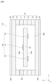
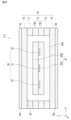
- FIG. 1 is an external perspective view of a multilayer substrate 100.
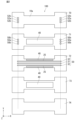
- FIG. 2 is a top view of each layer of the multilayer substrate 100 when viewed from the thickness direction.
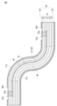
- FIG. 3 is a cross-sectional view of the multilayer substrate 100 after deformation according to the first embodiment.
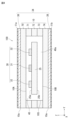
- 4 is a sectional view taken along line AA of the multilayer substrate 100
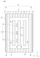
- FIG. 5 is a sectional view taken along line BB of the multilayer substrate 100.
- direction is defined as follows.
- the X-axis direction corresponds to the substrate stretching direction S of the multilayer substrate 100
- the Y-axis direction corresponds to the width direction W of the multilayer substrate 100
- the Z-axis direction corresponds to the thickness direction T of the multilayer substrate 100.
- the substrate stretching direction S is the direction in which the multilayer substrate 100 extends when viewed in the thickness direction T.
- the width direction W is a direction perpendicular to the direction in which the multilayer substrate 100 extends when viewed in the thickness direction T.
- the thickness direction T is the lamination direction in which at least one flexible resin layer 70 is laminated.
- the thickness direction T, the width direction W, and the substrate stretching direction S are orthogonal to each other. Note that the thickness direction T, width direction W, and substrate stretching direction S in this specification do not have to match the thickness direction, width direction, and signal transmission direction when the multilayer substrate 100 is actually used.
- a and B are electrically connected means that electricity can be conducted between A and B. Therefore, A and B may be in contact with each other, or A and B may not be in contact with each other. For example, when a conductive C is placed between A and B, A and B are electrically connected via C even if A and B are not in contact with each other.
- a and B are in contact means that A and B are connected in a contacting state.
- first and second are used only for descriptive purposes, and are not used to express or imply relative importance or ranking of technical features. Not to be understood.
- Features defined as “first” and “second” are expressly or implied to include one or more such features.
- the structure of the multilayer substrate 100 will be explained with reference to FIG. 1.
- the multilayer substrate 100 is a multilayer substrate for transmitting high frequency signals.
- the multilayer board 100 is, for example, a multilayer board for electrically connecting two circuits in an electronic device such as a smartphone.
- the multilayer substrate 100 has flexibility and can be bent as appropriate.
- the multilayer substrate 100 of the first embodiment has a shape extending in the substrate stretching direction S, as shown in FIG.
- the multilayer substrate 100 includes a laminate 10, a first inner layer resin 25, a plurality of conductors 30, and a conductive shield material 34.
- the laminate 10 has a plate shape with a first main surface 10a and a second main surface 10b separated in the thickness direction T. Specifically, the first main surface 10a and the second main surface 10b are opposed to each other.
- the first principal surface 10a may be referred to as an upper principal surface
- the second principal surface 10b may be referred to as a lower principal surface.
- a space 40 is provided inside the laminate 10.
- the laminate 10 has a plurality of laminated flexible resin layers 70, 71, 72, 73, and 74.
- the flexible resin layers 70, 71, 72, 73, and 74 are laminated along the thickness direction T. Specifically, the flexible resin layers 70, 71, 72, 73, and 74 are laminated in this order in the direction from the first main surface 10a to the second main surface 10b.
- the flexible resin layers 70, 71, 72, 73, and 74 have plate shapes with substantially the same dimensions. In this embodiment, in the thickness direction T, the outer surface of the flexible resin layer 70 forms the first main surface 10a, and the outer surface of the flexible resin layer 74 forms the second main surface 10b. are doing.
- the space 40 can be provided, for example, by removing a portion of the flexible resin layers 71, 72, and 73.
- the flexible resin layers 71, 72, and 73 are provided with holes that form the spaces 40.
- the flexible resin layers 71, 72, 73 are provided with, for example, rectangular holes.
- the flexible resin layers 70 and 74 are not provided with holes and have a continuous shape.
- the plurality of holes provided in the flexible resin layers 71, 72, 73 communicate in the thickness direction T.
- the flexible resin layers 71, 72, 73 are sandwiched between the flexible resin layers 70, 74 in the thickness direction T.
- the flexible resin layer 70 closes the hole openings in the flexible resin layer 71, and the flexible resin layer 74 closes the hole openings in the flexible resin layer 73.
- a space 40 formed by a plurality of consecutive holes is formed inside the laminate 10.
- the space 40 is formed into a rectangular shape when viewed in the thickness direction T. Air exists in the space 40.
- the flexible resin layers 70, 71, 72, 73, and 74 are, for example, flexible dielectric sheets.
- the material of the flexible resin layers 70, 71, 72, 73, and 74 is a thermoplastic resin.
- the thermoplastic resin include liquid crystal polymer, PTFE (polytetrafluoroethylene), and the like.
- the material of the flexible resin layers 70, 71, 72, 73, and 74 may be thermosetting resin or polyimide.
- the thermosetting resin is, for example, polyimide.
- the laminate 10 has an inner surface defining a space 40. More specifically, the laminate 10 includes a first inner wall 10A facing the first main surface 10a, a second inner wall 10B facing the second main surface 10b, and an inner wall 10S connecting them.
- the first inner wall 10A is defined by the flexible resin layer 70. Specifically, the first inner wall 10A is the inner surface of the flexible resin layer 70 on the side connected to the flexible resin layer 71. The first inner wall 10A is formed on the opposite side to the first main surface 10a formed on the flexible resin layer 71.
- the second inner wall 10B is defined by a flexible resin layer 74. Specifically, the second inner wall 10B is the inner surface of the flexible resin layer 74 on the side connected to the flexible resin layer 73. The second inner wall 10B is formed on the opposite side to the second main surface 10b formed on the flexible resin layer 74.
- the inner wall 10S is defined by flexible resin layers 71, 72, and 73. Specifically, the inner wall 10S is formed by a plurality of inner wall surfaces defining holes formed in the flexible resin layers 71, 72, and 73. Although the space 40 is defined by a plurality of inner walls in this embodiment, it may be defined by one inner wall. For example, a spherical inner wall can be mentioned.
- the first inner layer resin 25 is arranged in the space 40 of the laminate 10.
- the first inner layer resin 25 has a sheet shape extending in the substrate stretching direction S of the multilayer substrate 100.
- the first inner layer resin 25 has a third main surface 25a and a fourth main surface 25b that are separated in the thickness direction T.
- the first inner layer resin 25 is made of a flexible resin. Therefore, it can be bent by applying an external force. For example, when force is applied to the outside of the laminate 10, the first inner layer resin 25 deforms to curve within the space 40, as shown in FIG.
- the first inner layer resin 25 extends in the extending direction of the signal conductor 31 and is connected to the laminate 10 in the extending direction.
- the first inner layer resin 25 is connected to the laminate 10 in the substrate stretching direction S of the multilayer substrate 100.
- both ends of the first inner layer resin 25 in the substrate stretching direction S of the multilayer substrate 100 are connected to the inner wall 10S of the laminate 10.
- the first inner layer resin 25 is separated from the laminate 10 within the space 40. Specifically, in the cross section in the direction (Z direction) perpendicular to the direction in which the signal conductor 31 extends, the first inner layer resin 25 in the space 40 covers the first inner wall 10A, the second inner wall 10B, and the inner wall of the laminate 10. 10S and floating from the stacked body 10. That is, in a cross section in a direction (Z direction) perpendicular to the extending direction of the signal conductor 31, a hollow portion 40a is formed inside the laminate 10 to surround the first inner layer resin 25 in an annular shape. For example, the hollow portion 40a is filled with air.
- first inner layer resin 25 may be in contact with the laminate 10.
- a portion of the first inner layer resin 25 may be in contact with the laminate 10 when the multilayer substrate 100 is bent. That is, it is sufficient that at least a portion of the first inner layer resin 25 is separated from the laminate 10 within the space 40 .
- the first inner layer resin 25 is formed integrally with the flexible resin layer 72. Therefore, the first inner resin layer 25 is made of the same resin as the flexible resin layer 72. In other words, the first inner layer resin 25 is constituted by a part of the laminate 10.
- the first inner layer resin 25 may be formed of a separate member from the flexible resin layer 72, or may be formed of a different material from the flexible resin layer 72.
- the plurality of conductors 30 are conductor patterns provided on a portion of the laminate 10 and the first inner layer resin 25, and extend along the substrate stretching direction S. As shown in FIG. 4, the plurality of conductors 30 are provided on the third main surface 25a of the first inner resin layer 25. As shown in FIG.
- the plurality of conductors 30 may be provided on at least one of the third main surface 25a or the fourth main surface 25b of the first inner layer resin 25.
- the plurality of conductors 30 include a signal conductor 31 and a plurality of inner layer ground conductors 32.
- the plurality of conductors 30 are, for example, conductor layers formed by patterning metal foil pasted on the flexible resin layer 70.
- the metal foil is, for example, copper foil.
- the plurality of conductors may be formed by plating.
- the signal conductor 31 is a conductor for transmitting signals. In this embodiment, the signal conductor 31 transmits a high frequency signal.
- the signal conductor 31 is arranged with a gap between the two inner layer ground conductors 32.
- both ends of the signal conductor 31 in the substrate stretching direction S are arranged on a flexible resin layer 72 that defines the laminate 10. Specifically, both ends of the signal conductor 31 in the substrate stretching direction S are arranged in a portion of the flexible resin layer 72 on which the flexible resin layer 71 is laminated. Both ends of the signal conductor 31 in the substrate stretching direction S are connected to interlayer connection conductors 50a provided on the flexible resin layers 70 and 71.
- the interlayer connection conductor 50a is a conductor placed in a through hole provided in the thickness direction of the flexible resin layers 70 and 71.
- the interlayer connection conductor 50a is connected to a lead conductor 52a provided on the first main surface 10a of the flexible resin layer 70.
- the lead conductor 52a is arranged in the conductive shield material 34 arranged on the first main surface 10a of the laminate 10 and in the opening 46a provided in the protective film 11a.
- Each of the plurality of inner layer ground conductors 32 is a conductor connected to a ground potential. As shown in FIG. 2, the plurality of inner layer ground conductors 32 are arranged at intervals with the signal conductor 31 sandwiched therebetween. Both ends of the plurality of inner-layer ground conductors 32 in the substrate stretching direction S are arranged in the flexible resin layer 72 that defines the laminate 10, similarly to the signal conductor 31. Specifically, both ends of the plurality of inner layer ground conductors 32 in the substrate stretching direction S are arranged in the portion of the flexible resin layer 72 on which the flexible resin layer 71 is laminated. Both ends of the plurality of inner layer ground conductors 32 in the substrate stretching direction S are connected to interlayer connection conductors 50b provided on the flexible resin layer 71.
- the interlayer connection conductor 50b is a conductor placed in a through hole provided in the thickness direction of the flexible resin layers 70 and 71.
- the interlayer connection conductor 50b is connected to a lead-out conductor 52b provided on the flexible resin layer 70.
- the lead conductor 52b is arranged in the conductive shield material 34 arranged on the first main surface 10a of the laminate 10 and in the opening 46b provided in the protective film 11a.
- the conductive shield material 34 is provided on the first main surface 10a and the second main surface 10b of the laminate 10.
- the conductive shield material 34 is a film-like conductor that is provided on the flexible resin layers 70 and 74 and covers the main surfaces of the flexible resin layers 70 and 74 in the thickness direction, respectively. It's a pattern.
- the conductive shield material 34 is a conductive layer formed by patterning metal foil pasted on the flexible resin layers 70 and 74.
- the metal foil is, for example, copper foil.
- the conductive shield material 34 includes a first ground conductor 36 and a second ground conductor 38.
- the first ground conductor 36 is arranged on the first main surface 10a of the laminate 10.
- the second ground conductor 38 is arranged on the second main surface 10b of the laminate 10.
- the first ground conductor 36 and the second ground conductor 38 are each conductors connected to the ground potential.
- the first ground conductor 36 and the second ground conductor 38 have the role of suppressing the influence of noise from the outside world on the signal conductor 31, for example.
- Protective films 11a and 11b are arranged on the surface of the conductive shield material 34.
- the protective film 11a is, for example, a protective layer for protecting the first ground conductor 36 disposed on the first main surface 10a of the laminate 10.
- the protective film 11b is, for example, a protective layer for protecting the second ground conductor 38 disposed on the second main surface 10b of the laminate 10.
- the protective films 11a and 11b cover substantially the entire first main surface 10a and second main surface 10b of the stacked body 10, respectively.
- the protective films 11a and 11b are, for example, resin resists applied to the laminate 10. Note that the protective films 11a and 11b may be coverlays that are pasted on the laminate 10.
- the protective film 11a is provided with a plurality of openings 46a and 46b.
- the openings 46a and 46b are provided to connect the plurality of conductors 30 to the outside.
- lead conductors 52a and 52b electrically connected to the plurality of conductors 30 are arranged in the plurality of openings 46a and 46b.
- the first inner layer resin 25 overlaps the space 40 when viewed from the thickness direction T.
- the space 40 is provided at a position sandwiching the first inner layer resin 25 in the thickness direction T and in the width direction W.
- the first inner layer resin 25 is spaced apart from the inner surface of the laminate 10 in the thickness direction and in the width direction W. Specifically, the first inner layer resin 25 is separated from the first inner wall 10A and the second inner wall 10B in the thickness direction T. Further, the first inner layer resin 25 is separated from the inner wall 10S in the width direction W, but is connected to the inner wall 10S in the substrate stretching direction S.
- the plurality of conductors 30 are arranged to face the first ground conductor 36 and the second ground conductor 38 when viewed from the thickness direction T.
- the multilayer substrate 100 it is possible to suppress fluctuations in the clearance between the plurality of conductors 30 due to deformation of the multilayer substrate 100.
- the outer portion of the laminate 10 is curved and deformed, as shown in FIG.
- the plurality of conductors 30 are not arranged in the first inner layer resin 25 and only the conductor pattern is arranged in the space 40, there is a possibility that the degree of deformation of the plurality of conductors 30 will be different. In that case, it is conceivable that the clearance between the plurality of conductors 30 will vary and the signal characteristics will deteriorate.
- the multilayer substrate 100 includes a laminate 10, a first inner layer resin 25, and a plurality of conductors 30.
- the laminate 10 has a plurality of laminated flexible resin layers 70 to 74, and has a space 40 provided therein.
- the first inner layer resin 25 is arranged in the space 40 of the laminate 10 .
- the plurality of conductors 30 include signal conductors and are arranged in the first inner layer resin 25. With such a configuration, the plurality of conductors 30 deform along with the deformation of the first inner layer resin 25, so that the plurality of conductors 30 can easily undergo similar deformation. This makes it difficult for differences in deformation to occur between the plurality of conductors 30. As a result, even if the multilayer substrate 100 is deformed, fluctuations in the clearance between the plurality of conductors 30 can be suppressed.
- the signal conductor 31 is for high frequency signals, and high frequency signals are transmitted. This can be expected to suppress deterioration of signal characteristics by suppressing changes in clearance with the inner layer ground conductor 32. Note that a signal different from the high frequency signal, such as a low frequency signal, may be transmitted to the signal conductor 31.
- interlayer connection conductors 50a, 50b and lead-out conductors 52a, 52b are provided in flexible resin layers 70, 71 on one side and the other side of the laminate 10 in the substrate stretching direction S. did.
- the lead conductors 52a and 52b are arranged in the conductive shield material 34 arranged on the first main surface 10a of the laminate 10 and in the openings 46a and 46b provided in the protective film 11a.
- the interlayer connection conductors 50a, 50b and the lead-out conductors 52a, 52b may be provided in the flexible resin layers 73, 74 on at least one of one side or the other side of the laminate 10 in the substrate stretching direction S.
- openings 46a and 46b may be provided in the conductive shield material 34 and the protective film 11a disposed on the second main surface 10b of the laminate 10.
- the lead conductors 52a and 52b may be arranged in the conductive shield material 34 and the openings 46a and 46b provided in the protective film 11a, which are arranged on the second main surface 10b of the laminate 10.
- FIG. 6 is a longitudinal cross-sectional view of the multilayer substrate 101 according to the first modification.
- the multilayer substrate 101 according to the first modification differs from the multilayer substrate 100 according to the first embodiment in that it does not include the first ground conductor 36 and the second ground conductor 38.
- the multilayer substrate 101 has a structure in which protective films 11a and 11b are laminated on the laminate 10 in the thickness direction T. Specifically, a protective film 11a is laminated on the first main surface 10a of the laminate 10, and a protective film 11b is laminated on the second main surface 10b.
- FIG. 7 is a longitudinal cross-sectional view of a multilayer substrate 102 according to a second modification.
- the multilayer substrate 102 according to the second modification differs from the multilayer substrate 100 according to the first embodiment in the configuration of the plurality of conductors 30.
- the plurality of conductors 30 include one signal conductor 31 and one inner layer ground conductor 32.
- the configuration of the plurality of conductors 30 is not limited to the configurations of the first embodiment and the second modification.
- the plurality of conductors 30 may have any configuration as long as the characteristics are affected by the clearance between the plurality of conductors 30.
- the plurality of conductors 30 may have two signal conductors 31, and the two signal conductors 31 may constitute a differential line. Furthermore, two inner layer ground conductors 32 may be placed at positions sandwiching the differential line therebetween.
- FIG. 8 is a partially enlarged view of the multilayer substrate 103 according to the second embodiment.
- FIG. 8 shows an enlarged view of a part of the first inner resin layer 25 provided with a plurality of conductors 30. As shown in FIG.
- the multilayer substrate 103 according to the second embodiment is different from the multilayer substrate 100 according to the first embodiment in the width of the signal conductor 31 and the width of the inner layer ground conductor 32.
- the signal conductor 31 has a first portion 41 and a second portion 42.
- the width of the first portion 41 is larger than the width of the second portion 42 when viewed from the thickness direction T.
- two second portions 42 are connected to both ends of the first portion 41. That is, the first portion 41 is sandwiched between the two second portions 42.
- the first portion 41 is located in the space 40 of the laminate 10. Specifically, the first portion 41 is located in the first region R1 in which the space 40 is formed within the laminate 10 when viewed from the thickness direction T of the laminate 10.
- the first region R1 is a region defined by the inner wall 10S of the laminate 10 when viewed from the thickness direction T.
- the second portion 42 is not located in the space 40 within the laminate 10.
- the second portion 42 is located in a second region R2 in the laminate 10 in which the space 40 is not formed, when viewed from the thickness direction T of the laminate 10.
- the second region R2 is a region located outside the first region R1 when viewed from the thickness direction T, and is a region where the flexible resin layer 72 is arranged.
- the second region R2 is disposed outside the first region R1 in the substrate stretching direction S when viewed in the thickness direction T. Therefore, the second portion 42 extends from the inside of the laminate 10 toward the space 40 and is connected to the first portion 41 when viewed from the thickness direction T.
- the width of the first portion 41 is 1.1 times or more and 3.0 times or less than the width of the second portion 42.
- the width of the first portion 41 may be the maximum dimension in the width direction W when viewed from the thickness direction T.
- the width of the second portion 42 may be the minimum dimension in the width direction W when viewed from the thickness direction T.
- the inner layer ground conductor 32 has a third portion 43 and a fourth portion 44 that is wider than the third portion 43.
- two fourth portions 44 are connected to both ends of the third portion 43. That is, the third portion 43 is sandwiched between the two fourth portions 44.
- the third portion 43 is located in the space 40 within the laminate 10. Similar to the first portion 41, the third portion 43 is located in the first region R1 when viewed from the thickness direction T of the laminate 10.
- the fourth portion 44 is not located in the space 40 within the laminate 10. Similar to the second portion 42, the fourth portion 44 is located in the second region R2 when viewed from the thickness direction T of the laminate 10. Therefore, the fourth portion 44 extends from the inside of the laminate 10 toward the space 40 and is connected to the third portion 43 when viewed from the thickness direction T.
- the multilayer substrate 103 can be made smaller.
- the width of the fourth portion 44 of the inner layer ground conductor 32 may be larger than the width of the second portion 42 of the signal conductor 31.
- the width of the second portion 42 and the width of the fourth portion 44 refer to dimensions in the width direction W when viewed from the thickness direction T.
- the present invention is not limited to this.
- the width of the inner layer ground conductor 32 may be constant.
- FIG. 9 is a longitudinal cross-sectional view of the multilayer substrate 104 according to the third embodiment.
- the multilayer substrate 104 according to the third embodiment differs from the multilayer substrate 100 according to the first embodiment in the configuration of the laminate 10 and the position of the first inner layer resin 25.
- the laminate 10 further includes a flexible resin layer 75.
- Flexible resin layer 75 is arranged between flexible resin layers 73 and 74.
- the flexible resin layer 75 has the same shape as the flexible resin layer 73, for example.
- the first inner layer resin 25 is unevenly distributed with respect to the multilayer substrate 104 in the thickness direction T of the multilayer substrate 104.
- the first inner resin layer 25 is located closer to the flexible resin layer 70 than the flexible resin layer 74 .
- the first inner layer resin 25 is disposed at a position closer to the first main surface 10a of the laminate 10 than the second main surface 10b in the thickness direction T.
- the distance between the first inner wall 10A of the laminate and the third main surface 25a of the first inner layer resin 25 is the same as the distance between the second inner wall 10B of the laminate 10 and the fourth main surface of the first inner layer resin 25. It is smaller than the distance from the surface 25b.
- the bending stress of the first inner layer resin 25 depends on the distance from the bending neutral line.
- compressive stress is generated on the inner circumferential side of the bent portion, and tensile stress is generated on the outer circumferential side of the bent portion.
- the compressive stress and the tensile stress become smaller toward the inner center in the thickness direction of the first inner layer resin 25, and there is a position where the compressive stress and the tensile stress become zero. This position is called the bending neutral line.
- the bending neutral line When the distance from this bending neutral line is zero, the bending stress is zero, and the farther the distance is, the larger the bending stress becomes. Since the first inner layer resin 25 is located away from the laminate 10 within the space 40, the bending stress can be reduced even if the first inner layer resin 25 is located away from the bending neutral line.
- the first inner layer resin 25 is unevenly distributed in the thickness direction T by adding one flexible resin layer 75 to the laminate 10, but the present invention is not limited to this.
- the first inner layer resin 25 may be unevenly distributed in the thickness direction T by increasing the thickness of the flexible resin layer 73.
- the first inner layer resin 25 may be unevenly distributed in the thickness direction T by adding one or more flexible resin layers 75.
- the flexible resin layer 75 has the same shape as the flexible resin layer 73 has been described, but the present invention is not limited to this.
- the flexible resin layer 75 may have a different shape and thickness from the flexible resin layer 73.
- the first inner layer resin 25 is arranged at a position closer to the flexible resin layer 70 than the flexible resin layer 74 in the thickness direction T, but the present invention is not limited to this.
- the first inner resin layer 25 may be placed closer to the flexible resin layer 74 than the flexible resin layer 70 in the thickness direction T.
- FIG. 10 is a longitudinal cross-sectional view of a multilayer substrate 105 according to the fourth embodiment.
- the multilayer substrate 105 according to the fourth embodiment is different from the multilayer substrate 100 according to the first embodiment in the configuration of the laminate 10 and in that it further includes a plurality of second inner layer resins 26.
- the laminate 10 further includes flexible resin layers 77, 78, 79, and 80.
- Flexible resin layers 77 and 78 are arranged between flexible resin layers 71 and 72.
- Flexible resin layers 79 and 80 are arranged between flexible resin layers 72 and 73.
- the flexible resin layers 77 and 80 have the same shape as the flexible resin layer 72, for example.
- the flexible resin layers 78 and 79 have the same shape as the flexible resin layer 71, for example.
- the multilayer substrate 105 further includes a plurality of second inner layer resins 26.
- the plurality of second inner layer resins 26 have the same shape as the first inner layer resin 25, for example.
- the plurality of second inner layer resins 26 are arranged in the space 40 of the laminate 10. Specifically, in the space 40 of the laminate 10, a plurality of second inner layer resins 26 are arranged at intervals in the thickness direction T of the laminate 10.
- the first inner layer resin 25 is arranged between the plurality of second inner layer resins 26 in the thickness direction T. More specifically, the plurality of second inner layer resins 26 are located between the third main surface 25a of the first inner layer resin 25 and the first inner wall 10A of the laminate 10, and between the fourth main surface of the first inner layer resin 25. 25b and the second inner wall 10B of the laminate 10.
- the plurality of second inner layer resins 26 are each formed integrally with the flexible resin layers 77 and 80. Therefore, the plurality of second inner resin layers 26 are made of the same resin as the flexible resin layers 77 and 80. In other words, the plurality of second inner layer resins 26 are constituted by a part of the laminate 10.
- the plurality of second inner layer resins 26 are connected to the laminate 10 in the substrate stretching direction S of the multilayer substrate 100. Specifically, the plurality of second inner layer resins 26 are separated from the first inner wall 10A and the second inner wall 10B in the thickness direction T. The plurality of second inner layer resins 26 are separated from the inner wall 10S in the width direction W, while being connected to the inner wall 10S in the substrate stretching direction S.
- the multilayer board 105 since the multilayer board 105 includes the plurality of second inner layer resins 26, the first inner layer resin 25 and the plurality of conductors 30 come close to the first ground conductor 36 and the second ground conductor 38. suppress things. For example, when the multilayer substrate 105 is deformed, the first inner layer resin 25 comes into contact with the second inner layer resin 26, so the distance between the plurality of conductors 30 and the first ground conductor 36 and the second ground conductor becomes smaller. can be suppressed. Thereby, fluctuations in impedance of the plurality of conductors 30 can be suppressed.
- the multilayer substrate 105 may include one or more second inner layer resins 26.
- the multilayer substrate 105 may be arranged in a space 40 that becomes a mountain fold side with respect to the first inner layer resin 25 when the multilayer substrate 105 is bent. .
- FIG. 11A is a vertical cross-sectional view of the multilayer substrate 106 according to the fifth embodiment.
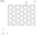
- FIG. 11B is a partially enlarged view showing an example of the plurality of first through holes 60 provided in the laminate 10.
- the multilayer substrate 106 according to the fifth embodiment is different from the multilayer substrate 105 according to the fourth embodiment in the structures of the flexible resin layers 70A to 78A, the first inner layer resin 25A, and the second inner layer resin 26A.
- a plurality of first through holes 60 are provided throughout the laminate 10, the first inner layer resin 25A, and the second inner layer resin 26A.
- the laminate 10 has flexible resin layers 70A to 74A and flexible resin layers 77A to 80A.
- the flexible resin layers 70A to 74A and the flexible resin layers 77A to 80A are different from each other, except that the plurality of first through holes 60 are provided.
- Each of the layers 77 to 80 has a similar shape.
- the plurality of first through holes 60 are regularly provided holes. Specifically, the plurality of first through holes 60 have substantially the same shape and size, and are provided at equal intervals. For example, the plurality of first through holes 60 are provided in a matrix when viewed from the thickness direction T.
- the shape of the plurality of first through holes 60 has, for example, a circular shape when viewed from the thickness direction T.
- the plurality of first through holes 60 have an opening width of, for example, 81 ⁇ m or more and 500 ⁇ m or less.
- the "opening width" refers to the maximum dimension of the first through hole 60.
- the opening width means the maximum diameter of the first through hole 60 when viewed from the thickness direction T.
- the distance between the plurality of first through holes 60 is, for example, 73 ⁇ m or more and 730 ⁇ m or less.
- the flexible resin layers 70A to 74A, the flexible resin layers 77A to 80A, the first inner resin layer 25A, and the second inner resin layer 26A are each made of, for example, a mesh member.
- the plurality of first through holes 60 are provided using, for example, a laser.
- the plurality of first through holes 60 are not holes of interlayer connection conductors such as via conductors. Therefore, air exists inside the first through hole 60.
- the amount of resin included in the multilayer substrate 106 is reduced. This makes the multilayer substrate 106 easier to bend, improving usability.
- a plurality of first through holes 60 may be provided in at least a portion of the laminate 10, the first inner layer resin 25A, or the second inner layer resin 26A.
- the plurality of first through holes 60 may be provided in some parts of the flexible resin layers 70A, 74A of the laminate 10, and the plurality of first through holes 60 may not be provided in other parts. Good too.
- a plurality of first through holes 60 may be provided in a part of the first inner layer resin 25A or the second inner layer resin 26A.
- a plurality of first through holes 60 may be provided at positions overlapping with the signal conductors 31 when viewed in the thickness direction T of the laminate 10. This reduces the dielectric constant and dielectric loss tangent around the signal conductor 31, and improves electrical characteristics.
- the shape of the plurality of first through holes 60 is not limited, and may be, for example, a triangular pyramid shape. Furthermore, the shape when viewed from the thickness direction T is not limited, and may be, for example, an ellipse.
- a plurality of first through holes 60 are provided throughout A of the flexible resin layers 70A to 74A, the flexible resin layers 77A to 80A, the first inner layer resin 25A, and the second inner layer resin 26. Not limited. Further, it is limited that the plurality of first through holes 60 are provided in each of the flexible resin layers 70A to 74A, the flexible resin layers 77A to 80A, the first inner layer resin 25A, and the second inner layer resin 26A. do not.
- the plurality of first through holes 60 do not have to be arranged regularly.
- the plurality of first through holes 60 may be provided randomly.
- the sizes or shapes of the plurality of first through holes 60 may be different.
- the second inner layer resin 26A is not an essential component.
- FIG. 11C is a partially enlarged cross-sectional view showing an example of a porous material.
- the multilayer substrate according to the modification of the fifth embodiment is different from the multilayer substrate 106 according to the fifth embodiment in that the laminate 10, the first inner layer resin 25A, and the second inner layer resin 26A are made of porous materials. differ.
- a porous material is a material that has a porous structure.
- the porous structure is a structure in which a plurality of air bubbles P are dispersed throughout the porous region A.
- the porous region A means a region in which a plurality of air bubbles P are provided in the element body 12 constituting the porous material.
- the porous region A is provided throughout the laminate 10, the first inner layer resin 25A, and the second inner layer resin 26A.
- the porous region A contains a plurality of closed cells.
- the closed cell has a structure in which the entire bubble P is surrounded by the material of the element body 12, so that the gas inside the bubble P cannot leak to the outside of the element body 12. Furthermore, in closed cells, adjacent cells P are not connected to each other.
- the porosity of the porous region A is, for example, 30% or more and 80% or less. The porosity is the ratio of the volume of the bubbles P to the entire volume of the element body 12.
- the present invention is not limited thereto.
- at least a portion of the laminate 10, the first inner layer resin 25A, or the second inner layer resin 26A may be made of a porous material.
- the porous region A may also be provided in at least a portion of the laminate 10, the first inner layer resin 25A, or the second inner layer resin 26A.
- FIG. 11D is a partially enlarged sectional view showing another example of the porous material. As shown in FIG. 11D, a plurality of bubbles Q may be connected and provided in the porous material. Moreover, the shapes and/or sizes of the plurality of bubbles Q may be different.
- FIG. 12A is a vertical cross-sectional view of the multilayer substrate 107 according to the sixth embodiment.
- FIG. 12B is a partially enlarged view showing an example of the plurality of second through holes 53 provided in the second inner layer resin 26B.
- the multilayer substrate 107 according to the sixth embodiment differs from the multilayer substrate 105 according to the fourth embodiment in the structure of the second inner layer resin 26B.
- a plurality of second through holes 53 are provided in the second inner layer resin 26B.
- a plurality of second through holes 53 are provided in each of the two second inner layer resins 26B.
- the plurality of second through holes 53 are provided at positions overlapping with the signal conductor 31 when viewed in the thickness direction T.
- the plurality of second through holes 53 are provided along the direction in which the signal conductor 31 extends, that is, the substrate extension direction S when viewed in the thickness direction T.
- the plurality of second through holes 53 have, for example, a circular shape when viewed in the thickness direction T.
- the length of the second through hole 53 in the width direction W is longer than the length of the signal conductor 31 in the width direction W.
- the second through hole 53 has an opening width of, for example, 1/6 or more and 1/3 or less of the length in the width direction W of the laminate 10.
- the "opening width” refers to the maximum dimension of the second through hole 53 in the width direction W of the laminate 10.
- the opening width means the maximum diameter of the second through hole 53.
- the portion where the second inner layer resin 26B is arranged in the region overlapping with the signal conductor 31 when seen in the thickness direction T can be reduced. Air having a lower dielectric constant than the second inner layer resin 26B exists in the plurality of second through holes 53. Therefore, the signal characteristics of the signal conductor 31 can be improved.
- the length of the second through hole 53 in the width direction W is longer than the length of the signal conductor 31 in the width direction W. With this configuration, the signal characteristics of the signal conductor 31 can be further improved.
- the multilayer substrate 107 includes two second inner layer resins 26B has been described, but the present invention is not limited to this.
- the multilayer substrate 107 may include one or more second inner layer resins 26B.
- second through holes 53 are provided in the second inner layer resin 26B
- the present invention is not limited to this.
- one or more second through holes 53 may be provided in the second inner layer resin 26B.
- one rectangular second through hole 53 may be provided in the second inner layer resin 26B.
- a plurality of second through holes 53 are provided in both of the two second inner layer resins 26B, but the present invention is not limited to this.
- a plurality of second through holes 53 may be provided in at least one of the two second inner layer resins 26B.
- the shape of the second through hole 53 is not limited, and may be, for example, triangular pyramid shape. Further, the shape of the second through hole 53 when viewed from the thickness direction T is not limited, and may be, for example, an ellipse, a rectangle, or a polygon.
- FIG. 13A is a vertical cross-sectional view of the multilayer substrate 108 according to the seventh embodiment.
- FIG. 13B is a partially enlarged view showing an example of the plurality of third through holes 54 provided in the flexible resin layer 70.
- the multilayer substrate 108 according to the seventh embodiment is different from the multilayer substrate 107 according to the sixth embodiment in the structure of the laminate 10.
- a plurality of third through holes 54 are further provided in the flexible resin layers 70 and 74.
- the plurality of third through holes 54 are provided at positions overlapping with the signal conductor 31 when viewed in the thickness direction T. Further, the plurality of third through holes 54 are provided along the direction in which the signal conductor 31 extends, that is, the substrate extension direction S when viewed in the thickness direction T.
- the plurality of third through holes 54 have, for example, a circular shape when viewed in the thickness direction T.
- the length of the through hole 54 in the width direction W is longer than the length of the signal conductor 31 in the width direction W.
- the third through hole 54 has an opening width that is, for example, 1/6 or more and 1/3 or less of the length in the width direction W of the laminate 10.
- the "opening width” refers to the maximum dimension of the third through hole 54 in the width direction W of the laminate 10.
- the opening width means the maximum diameter of the third through hole 54.
- the plurality of third through holes 54 are provided at positions overlapping with the plurality of through holes 53 provided in the second inner layer resin 26B when viewed in the thickness direction T.
- the plurality of third through holes 54 have the same shape, size, and arrangement as the plurality of through holes 53.
- the flexible resin layer 70 by providing the plurality of third through holes 54 in the flexible resin layers 70, 74, the flexible resin layer 70, The portion where 74 is arranged can be reduced. Air having a lower dielectric constant than the flexible resin layers 70 and 74 exists in the plurality of third through holes 54 . Therefore, in the multilayer substrate 108, the signal characteristics of the signal conductor 31 can be improved.
- the plurality of third through holes 54 are provided at positions overlapping with the plurality of through holes 53 provided in the second inner layer resin 26B. With such a configuration, the signal characteristics of the signal conductor 31 can be further improved.
- the length of the through hole 54 in the width direction W is longer than the length of the signal conductor 31 in the width direction W. As a result, the dielectric constant around the signal conductor 31 is reduced, so that the signal characteristics of the signal conductor 31 can be improved.
- a plurality of through holes 54 are provided in the flexible resin layers 70 and 74 , but the present invention is not limited to this.
- a plurality of third through holes 54 may be provided in at least one of the flexible resin layer 70 or 74.
- one or more third through holes 54 may be provided in the flexible resin layer 70 or 74.
- one rectangular third through hole 54 may be provided in the flexible resin layer 70 or 74.
- the plurality of third through holes 54 may have a shape, size, and arrangement different from those of the plurality of through holes 53.
- the shape of the through hole 54 is not limited, and may be, for example, triangular pyramid shape. Further, the shape of the third through hole 54 when viewed from the thickness direction T is not limited, and may be, for example, elliptical, rectangular, or polygonal.
- FIG. 14A is a vertical cross-sectional view of the multilayer substrate 109 according to the eighth embodiment.
- FIG. 14B is a partially enlarged view showing an example of the plurality of first protrusions 27 provided on the first inner layer resin 25.
- FIG. 14A is a vertical cross-sectional view of the multilayer substrate 109 according to the eighth embodiment.
- FIG. 14B is a partially enlarged view showing an example of the plurality of first protrusions 27 provided on the first inner layer resin 25.
- the multilayer substrate 109 according to the eighth embodiment is different from the multilayer substrate 100 according to the first embodiment in the configuration of the laminate 10 and in that it further includes a plurality of first protrusions 27.
- the laminate 10 further includes flexible resin layers 78 and 79.
- Flexible resin layer 78 is arranged between flexible resin layers 71 and 72
- flexible resin layer 79 is arranged between flexible resin layers 72 and 73.
- the flexible resin layers 78 and 79 have the same shape as the flexible resin layer 73, for example.
- the multilayer substrate 109 further includes a first protrusion 27.
- the first inner layer resin 25 has a plurality of first protrusions 27 that protrude in the thickness direction T of the laminate 10 . More specifically, the plurality of first protrusions 27 are provided on both the third main surface 25a and the fourth main surface 25b of the first inner layer resin 25 in the thickness direction T. The plurality of first protrusions 27 are formed with substantially the same shape and dimensions.
- each of the plurality of first protrusions 27 has a rectangular parallelepiped shape.
- the plurality of first protrusions 27 are arranged on the outer side of the plurality of conductors 30 when viewed in the thickness direction T. Specifically, when viewed in the thickness direction T, the plurality of first protrusions 27 are arranged on both outer sides of the plurality of conductors 30 in the width direction W in which the plurality of conductors 30 are lined up.
- the height of the plurality of first protrusions 27 in the thickness direction T is greater than the thickness of the plurality of conductors 30 in the thickness direction T. Further, the height of the plurality of first protrusions 27 in the thickness direction T is smaller than the distance between the first inner wall 10A of the laminate 10 and the third main surface 25a of the first inner layer resin 25 in the thickness direction T.
- the plurality of first protrusions 27 provided on the fourth main surface 25b of the first inner layer resin 25 are provided at positions overlapping with the plurality of first protrusions 27 provided on the third main surface 25a when viewed in the thickness direction T. There is. Further, on the fourth main surface 25b of the first inner layer resin 25, the height of the plurality of first protrusions 27 in the thickness direction T is the same as that of the second inner wall 10B of the laminate 10 in the thickness direction T. It is smaller than the distance between the four main surfaces 25b.
- the plurality of first protrusions 27 are located outside the two inner layer ground conductors 32. Specifically, when viewed in the thickness direction T, the plurality of first protrusions 27 are arranged between the end of the first inner layer resin 25 and the inner layer ground conductor 32 in the width direction W. The plurality of first protrusions 27 are arranged at intervals along the substrate stretching direction S. For example, the plurality of first protrusions 27 are arranged at equal intervals along the substrate stretching direction S.
- the multilayer substrate 109 includes the plurality of first protrusions 27, the first inner layer resin 25 and the plurality of conductors 30 do not approach the first ground conductor 36 and the second ground conductor 38. can be suppressed. Thereby, fluctuations in the impedance of the signal conductor 31 can be suppressed.
- the first inner layer resin 25 may be provided with one or more first protrusions 27 .
- one or more first protrusions 27 may be provided on the third main surface 25a or the fourth main surface 25b of the first inner layer resin 25.
- the plurality of first protrusions 27 may not be provided on both the third main surface 25a and the fourth main surface 25b of the first inner layer resin 25 in the thickness direction T.
- the plurality of first protrusions 27 may be provided on at least one of the third main surface 25a and the fourth main surface 25b of the first inner layer resin 25.
- it may be provided at least on the surface that becomes the mountain fold side when the multilayer substrate 109 is bent.
- the shape of the first protrusion 27 is not limited, and may be, for example, cylindrical or triangular pyramidal. Further, the shape of the cross section of the first protrusion 27 is not limited either.
- the first protrusion 27 may be placed outside the plurality of conductors 30.
- the first protrusion 27 may be arranged between the plurality of conductors 30.
- the width of the first protrusion 27 provided on the third main surface 25a of the first inner layer resin 25 is smaller than the interval between the plurality of conductors 30.
- the distance between the first protrusion 27 and the signal conductor 31 in the width direction W may be shorter than the distance between the inner layer ground conductor 32 and the signal conductor 31.
- the first protrusion 27 is closer to the signal conductor 31 than the inner layer ground conductor 32, so that fluctuations in impedance can be further suppressed.
- first protrusions 27 are arranged at equal intervals along the substrate stretching direction S, but the present invention is not limited to this.
- one continuous first protrusion 27 may be arranged along the substrate stretching direction S.
- the plurality of first protrusions 27 are formed with substantially the same shape and the same dimensions, but the present invention is not limited to this.
- the plurality of first protrusions 27 may be formed with different shapes or dimensions.
- FIG. 15A is a vertical cross-sectional view of the multilayer substrate 110 according to the ninth embodiment.
- FIG. 15B is a partially enlarged view showing an example of the plurality of second protrusions 28 provided on the second inner layer resin 26.
- the multilayer substrate 110 according to the ninth embodiment is different from the multilayer substrate 105 according to the fourth embodiment in the configuration of the laminate 10 and in that it further includes a plurality of second protrusions 28.
- the laminate 10 further includes flexible resin layers 81 and 82.
- Flexible resin layer 81 is arranged between flexible resin layers 71 and 77.
- Flexible resin layer 82 is arranged between flexible resin layers 80 and 73.
- the flexible resin layers 81 and 82 have the same shape as the flexible resin layer 73, for example.
- the multilayer substrate 110 further includes a plurality of second protrusions 28.
- the second inner layer resin 26 has a plurality of second protrusions 28 that protrude in the thickness direction T of the laminate 10.
- the plurality of second protrusions 28 are formed with substantially the same shape and the same dimensions.
- the plurality of second protrusions 28 are arranged at positions that do not overlap the signal conductors 31 when viewed in the thickness direction T.
- the plurality of second protrusions 28 are located between the inner layer ground conductor 32 and the conductive shield material 34.
- the plurality of second protrusions 28 are arranged at positions overlapping with the inner layer ground conductor 32 when viewed in the thickness direction T.
- the plurality of second protrusions 28 are arranged at intervals along the substrate stretching direction S.
- the plurality of second protrusions 28 are arranged at equal intervals along the substrate stretching direction S when viewed in the thickness direction T.
- each of the plurality of second protrusions 28 has a rectangular parallelepiped shape.
- the height of the plurality of second projections 28 in the thickness direction T is equal to the first inner wall 10A of the laminate 10. It is smaller than the distance between the second inner layer resin 26 and the second inner layer resin 26 .
- the height of the plurality of second protrusions 28 in the thickness direction T is determined by the second inner wall of the laminate 10. It is smaller than the distance between 10B and the second inner layer resin 26.
- the multilayer board 110 since the multilayer board 110 includes the plurality of second protrusions 28, the first inner layer resin 25 and the plurality of conductors 30 do not come close to the first ground conductor 36 or the second ground conductor 38. can be suppressed. Thereby, fluctuations in the impedance of the signal conductor 31 can be suppressed.
- the plurality of second protrusions 28 are arranged at positions that do not overlap with the signal conductor 31 when viewed in the thickness direction T. With such a configuration, the dielectric constant and dielectric loss tangent around the signal conductor 31 are reduced, and the electrical characteristics are improved.
- a plurality of second protrusions 28 are provided on each of the two second inner layer resins 26 , but the present invention is not limited to this.
- a plurality of second protrusions 28 may be provided on at least one second inner layer resin 26.
- a plurality of second protrusions 28 may be provided on the surface of the second inner layer resin 26 that becomes the mountain fold side when the multilayer substrate 110 is bent.
- the shape of the second protrusion 28 is not limited, and may be, for example, cylindrical or triangular pyramidal. Further, the cross-sectional shape of the second protrusion 28 is not limited either.
- the plurality of second protrusions 28 are provided at positions overlapping with the inner layer ground conductor 32 when viewed in the thickness direction T, but the present invention is not limited to this.
- the plurality of second protrusions 28 may be provided at positions that do not overlap the inner layer ground conductor 32 when viewed in the thickness direction T.
- the second inner layer resin 26 is provided with a plurality of second protrusions 28 , but the present invention is not limited to this.
- the second inner layer resin 26 may be provided with one or more second protrusions 28 .
- the plurality of second protrusions 28 are formed with substantially the same shape and the same dimensions, but the present invention is not limited to this.
- the plurality of second protrusions 28 may be formed with different shapes or dimensions.
- FIG. 16 is a longitudinal cross-sectional view of the multilayer substrate 111 according to the tenth embodiment.
- FIG. 17 is an exploded top view of the multilayer substrate 111 according to the tenth embodiment.
- FIG. 18 is a cross-sectional view of the multilayer substrate 111 after deformation according to the tenth embodiment.
- the multilayer substrate 111 according to the tenth embodiment is different from the multilayer substrate 100 according to the first embodiment in the configuration of the laminate 10 and in that it further includes a plurality of third protrusions 29.
- the laminate 10 further includes flexible resin layers 83 and 84.
- the flexible resin layer 83 is arranged between the flexible resin layers 70 and 71.
- Flexible resin layer 84 is arranged between flexible resin layers 73 and 74.
- the flexible resin layers 83 and 84 have the same shape as the flexible resin layer 73, for example.
- the multilayer substrate 111 further includes a plurality of third protrusions 29.
- the multilayer substrate 111 has a plurality of third protrusions 29 that protrude in the thickness direction T of the laminate 10 .
- the plurality of third protrusions 29 are provided on the inner surface of the laminate 10.
- the plurality of third protrusions 29 are provided on the first inner wall 10A and the second inner wall 10B of the stacked body 10.
- the plurality of third protrusions 29 provided on the first inner wall 10A of the laminate 10 protrude from the first inner wall 10A toward the third main surface 25a of the first inner layer resin 25 in the thickness direction T.
- the plurality of third protrusions 29 provided on the second inner wall 10B of the laminate 10 protrude from the second inner wall 10B toward the fourth main surface 25b of the first inner layer resin 25.
- the plurality of third protrusions 29 are arranged at positions that do not overlap with the signal conductors 31 when viewed in the thickness direction T.
- the plurality of third protrusions 29 are located between the inner layer ground conductor 32 and the conductive shield material 34.
- the plurality of third protrusions 29 are arranged at positions overlapping with the inner layer ground conductor 32 when viewed in the thickness direction T.
- the plurality of third protrusions 29 are arranged at intervals along the substrate stretching direction S.
- the plurality of third protrusions 29 are arranged at equal intervals along the substrate stretching direction S.
- the plurality of third protrusions 29 are formed with substantially the same shape and the same dimensions.
- each of the plurality of third protrusions 29 has a rectangular parallelepiped shape.
- the height of the plurality of third protrusions 29 in the thickness direction T is smaller than the distance between the inner surface of the laminate 10 and the first inner layer resin 25 in the thickness direction T.
- the height of the plurality of third protrusions 29 provided on the first inner wall 10A of the laminate 10 is smaller than the distance between the first inner wall 10A and the third main surface 25a of the first inner layer resin 25.
- the plurality of third protrusions 29 provided on the second inner wall 10B of the laminate 10 are smaller than the distance between the second inner wall 10B and the fourth main surface 25b of the first inner layer resin 25.
- the outer portion of the laminate 10 is curved and deformed.
- the first inner layer resin 25 and the plurality of conductors 30 deform.
- the plurality of third protrusions 29 protruding from the inner surface of the laminate 10 prevent the first inner layer resin 25 and the plurality of conductors 30 from approaching the first ground conductor 36 and the second ground conductor 38.
- the first inner layer resin 25 comes into contact with the plurality of third protrusions 29, thereby maintaining a state separated from the first ground conductor 36 and the second ground conductor 38.
- the multilayer substrate 111 includes the plurality of third protrusions 29, the first inner layer resin 25 and the plurality of conductors 30 do not approach the first ground conductor 36 and the second ground conductor 38. can be suppressed. Thereby, fluctuations in the impedance of the signal conductor 31 can be suppressed.
- the plurality of third protrusions 29 are arranged at positions that do not overlap with the signal conductor 31 when viewed in the thickness direction T. With such a configuration, the dielectric constant and dielectric loss tangent around the signal conductor 31 are reduced, and the electrical characteristics are improved.
- third protrusions 29 are provided on the inner surface of the laminate 10
- the present invention is not limited to this.
- one or more third protrusions 29 may be provided on the inner surface of the laminate 10.
- a plurality of third protrusions 29 are provided on both the first inner wall 10A and the second inner wall 10B of the laminate 10, but the present invention is not limited to this.
- the plurality of third protrusions 29 may be provided on at least one of the first inner wall 10A and the second inner wall 10B.
- it may be provided on the inner surface of the laminate 10 that becomes the mountain fold side when the multilayer substrate 111 is bent.
- the shape of the third protrusion 29 is not limited, and may be, for example, cylindrical or triangular pyramidal. Further, the shape of the cross section of the third protrusion 29 is not limited either.
- the third protrusion 29 may be arranged at a position that does not overlap the inner layer ground conductor 32 when viewed in the thickness direction T.
- the plurality of third protrusions 29 are formed with substantially the same shape and the same dimensions, but the present invention is not limited to this.
- the plurality of third protrusions 29 may be formed with different shapes or dimensions.
- FIG. 19 is a longitudinal cross-sectional view of the multilayer substrate 112 according to the eleventh embodiment.
- the multilayer board 112 according to the eleventh embodiment has the following advantages in the structure of the laminate 10 and in that the plurality of conductors 30 are provided on the third main surface 25a and the fourth main surface 25b of the first inner layer resin 25. This is different from the multilayer substrate 100 according to the embodiment.
- the laminate 10 includes flexible resin layers 71 to 76.
- Flexible resin layers 71-73 and 75-76 are arranged between flexible resin layers 70 and 74.
- the plurality of conductors 30 are provided on the third main surface 25a and the fourth main surface 25b of the first inner layer resin 25.
- the signal conductor 31 is provided on the third main surface 25a
- the inner layer ground conductor 32 is provided on the fourth main surface 25b.
- the plurality of conductors 30 do not need to be provided on the same surface of the first inner layer resin 25.
- the signal conductor 31 is provided on the third main surface 35a of the first inner layer resin 25, and the inner layer ground conductor 32 is provided on the fourth main surface 25b, but the present invention is not limited to this.
- the signal conductor 31 may be provided on the fourth main surface 25b, and the inner layer ground conductor 32 may be provided on the third main surface 25a.
- FIG. 20 is a longitudinal cross-sectional view of the multilayer substrate 113 according to the twelfth embodiment.
- the multilayer substrate 113 according to the twelfth embodiment is different from the multilayer substrate 100 according to the first embodiment in the structure of the laminate 10 and the plurality of conductors 30 embedded in the first inner layer resin 25.
- the laminate 10 includes flexible resin layers 71 to 74.
- Flexible resin layer 72 includes two flexible resin layers 72B and 72C.
- the flexible resin layer 72B is laminated on the flexible resin layer 72C.
- the flexible resin layers 72B and 72C form the first inner layer resin 25. That is, the first inner layer resin 25 is formed of a part of the flexible resin layers 72B and 72C.
- the first inner layer resin 25 includes an inner layer resin 25B and an inner layer resin 25C.
- the inner layer resin 25B is laminated on the inner layer resin 25C.
- the inner layer resin 25B is formed of a part of the flexible resin layer 72B.
- the inner layer resin 25C is formed of a part of the flexible resin layer 72C.
- a plurality of conductors 30 are embedded in the first inner layer resin 25. Specifically, the plurality of conductors 30 are covered with inner layer resin 25B and inner layer resin 25C.
- the plurality of conductors 30 are embedded in the first inner layer resin 25 and do not need to be exposed from the first inner layer resin 25.
- the quality of the multilayer board 113 can be improved.
- FIG. 21 is a longitudinal cross-sectional view of the multilayer substrate 114 according to the thirteenth embodiment.
- the multilayer substrate 114 according to the thirteenth embodiment is different from the multilayer substrate according to the first embodiment in that the structure of the laminate 10 and the first main surface 10a of the laminate 10 are arranged in contact with the wall surface of the housing 90. This is different from the substrate 100.
- the laminate 10 includes flexible resin layers 71 to 76.
- no ground conductor is provided on the first main surface 10a of the laminate 10, and the wall surface of the casing 90 is provided.
- the housing 90 is made of metal, for example.
- the housing 90 is, for example, a case for a battery pack. Note that the housing 90 may be made of a shielding material.
- the casing 90 may be arranged without providing a ground conductor on the first main surface 10a of the laminate 10. Even in such a configuration, the same effects as the multilayer substrate 100 of the first embodiment can be achieved.
- FIG. 22 is a longitudinal cross-sectional view of the multilayer substrate 115 according to the fourteenth embodiment.
- the multilayer substrate 115 according to the fourteenth embodiment differs from the multilayer substrate 100 according to the first embodiment in the structure of the laminate 10 and in that it includes two inner layer resins 25D and 25E on which a plurality of conductors 30 are provided.
- the laminate 10 includes flexible resin layers 71 to 74.
- the flexible resin layer 72 includes three flexible resin layers 72D, 72E, and 72F.
- the flexible resin layer 72F is laminated on the flexible resin layer 72E, and the flexible resin layer 72D is laminated on the flexible resin layer 72F. That is, the flexible resin layer 72F is provided between the flexible resin layers 72D and 72E.
- the first inner layer resin 25 includes two inner layer resins 25D and 25E.
- the two inner layer resins 25D and 25E are arranged with a space in the stacking direction (Z direction) of the stacked body 10.
- the inner layer resin 25D is formed of a part of the flexible resin layer 72D.
- the inner layer resin 25E is formed of a part of the flexible resin layer 72E.
- the inner layer resin 25D has a sheet shape extending in the substrate stretching direction S of the multilayer substrate 115.
- a plurality of conductors 30A are provided on the surface of the inner layer resin 25D.
- the plurality of conductors 30A include a signal conductor 31 and an inner layer ground conductor 32, and form a coplanar line.
- the inner layer resin 25E has a sheet shape extending in the substrate stretching direction S of the multilayer substrate 115.
- a plurality of conductors 30A are provided on the surface of the inner layer resin 25E.
- the plurality of conductors 30B include a signal conductor 31 and an inner layer ground conductor 32, and form a coplanar line.
- the first inner layer resin 25 has two inner layer resins 25D and 25F arranged with a space in the stacking direction (Z direction) of the laminate 10.
- the two inner layer resins 25D and 25F are provided with a plurality of conductors 30A and 30B, respectively. That is, in the first inner layer resin 25, two coplanar lines provided in the two inner layer resins 25D and 25F run in parallel in the stacking direction (Z direction). Even in such a configuration, the same effects as the multilayer substrate 100 of the first embodiment can be achieved.
- the first inner layer resin 25 includes two inner layer resins 25D and 25F provided with a plurality of conductors 30A and 30B
- the present invention is not limited thereto.
- the first inner layer resin 25 may include two or more inner layer resins, and each of the two or more inner layer resins may be provided with a plurality of conductors 30.
- the conductive shield material 34 may be provided by a conductive paste or a conductive seal. This configuration improves shielding performance.
- a conductive seal may be used as the conductive shield material 34.
- the conductive seal can improve shielding performance while closing the through holes 53 and 54.
- a conductive shielding material 34 such as a conductive paste or a conductive seal may be provided after the multilayer board is bent.
Landscapes
- Engineering & Computer Science (AREA)
- Microelectronics & Electronic Packaging (AREA)
- Physics & Mathematics (AREA)
- Electromagnetism (AREA)
- Production Of Multi-Layered Print Wiring Board (AREA)
- Structure Of Printed Boards (AREA)
Abstract
Description
積層された複数の可撓性樹脂層を有し、内部に空間が設けられた積層体と、
前記積層体の前記空間に配置される第1内層樹脂と、
信号導体を含み、前記第1内層樹脂に配置される複数の導体と、
を備え、
前記第1内層樹脂の少なくとも一部は、前記積層体から離れている。
積層体10は、厚み方向Tに離れた第1主面10aおよび第2主面10bを有する板形状を有している。具体的には、第1主面10aと第2主面10bとは対向している。本明細書では、第1主面10aは上主面と称し、第2主面10bは下主面と称してもよい。
第1内層樹脂25は、積層体10の空間40に配置されている。第1内層樹脂25は、多層基板100の基板延伸方向Sに延びるシート形状を有する。第1内層樹脂25は、厚み方向Tに離れた第3主面25aと第4主面25bを有している。
図2に示すように、複数の導体30は、積層体10の一部および第1内層樹脂25に設けられた導体パターンであり、基板延伸方向Sに沿って延びる。図4に示すように、複数の導体30は、第1内層樹脂25の第3主面25aに設けられている。
図4に示すように、導電性シールド材34は、積層体10の第1主面10aと第2主面10bとに設けられている。具体的には、導電性シールド材34は、可撓性樹脂層70,74に設けられており、可撓性樹脂層70,74の厚み方向における主面をそれぞれ覆っている、膜状の導体パターンである。導電性シールド材34は、可撓性樹脂層70,74に張り付けられた金属箔にパターニングが施されることにより形成された導体層である。金属箔は、例えば、銅箔である。
以下に、第1実施形態の第1変形例に係る多層基板について図面を参照しながら説明する。第1実施形態の第1変形例においては、第1実施形態と重複する内容について適宜、説明を省略する。以降の変形例および実施形態でも同様である。
以下に、第1実施形態の第2変形例に係る多層基板について図面を参照しながら説明する。
以下に、第2実施形態に係る多層基板について図面を参照しながら説明する。
以下に、第3実施形態に係る多層基板について図面を参照しながら説明する。
以下に、第4実施形態に係る多層基板について図面を参照しながら説明する。
以下に、第5実施形態に係る多層基板について図面を参照しながら説明する。
以下に、第5実施形態の変形例に係る多層基板について図11Cを用いて説明する。
以下に、第6実施形態に係る多層基板について図面を参照しながら説明する。
以下に、第7実施形態に係る多層基板について図面を参照しながら説明する。
以下に、第8実施形態に係る多層基板について図面を参照しながら説明する。
以下に、第9実施形態に係る多層基板について図面を参照しながら説明する。
以下に、第10実施形態に係る多層基板について図面を参照しながら説明する。
以下に、第11実施形態に係る多層基板について図面を参照しながら説明する。
以下に、第12実施形態に係る多層基板について図面を参照しながら説明する。
以下に、第13実施形態に係る多層基板について図面を参照しながら説明する。
以下に、第14実施形態に係る多層基板について図面を参照しながら説明する。
以上のように、本出願において開示する技術の例示として、上記の実施形態や変形例を説明した。しかしながら、本開示における技術は、これに限定されず、適宜、変更、置き換え、付加、省略などを行った実施形態にも適用可能である。そこで、以下、他の実施形態を例示する。
11a,11b:保護膜
25:第1内層樹脂
26,26A,26B:第2内層樹脂
27:第1突起
28:第2突起
29:第3突起
30,30A,30B:複数の導体
31:信号導体
32:内層グランド導体
34:導電性シールド材
36:第1グランド導体
38:第2グランド導体
40:空間
41:第1部分
42:第2部分
43:第3部分
44:第4部分
50:層間接続導体
52:引出導体
53:第2貫通孔
54:第3貫通孔
60:第1貫通孔
70~84:可撓性樹脂層
100~115:多層基板
S:基板延伸方向
T:厚み方向
Claims (19)
- 積層された複数の可撓性樹脂層を有し、内部に空間が設けられた積層体と、
前記積層体の前記空間に配置される第1内層樹脂と、
信号導体を含み、前記第1内層樹脂に配置される複数の導体と、
を備え、
前記第1内層樹脂の少なくとも一部は、前記空間内において、前記積層体から離れている、
多層基板。 - 前記積層体又は前記第1内層樹脂のうちの少なくとも一部には、複数の第1貫通孔が設けられている、
請求項1に記載の多層基板。 - 前記複数の第1貫通孔は、前記第1内層樹脂において、前記積層体の積層方向に見て前記信号導体と重なる位置に設けられている、
請求項2に記載の多層基板。 - 前記第1内層樹脂は、前記積層体の積層方向に突出する第1突起を有する、
請求項1から3のいずれか1項に記載の多層基板。 - 前記第1突起は、前記複数の導体が並ぶ方向において前記複数の導体の外側に配置される、
請求項4に記載の多層基板。 - 前記積層体の前記空間において、前記積層体の積層方向に間隔を有して配置される複数の第2内層樹脂をさらに備え、
前記第1内層樹脂は、前記複数の第2内層樹脂の間に配置される、
請求項1から5のいずれか1項に記載の多層基板。 - 前記複数の第2内層樹脂の少なくとも1つは、前記積層方向に突出する第2突起を有する、
請求項6に記載の多層基板。 - 前記第2突起は、前記積層体の積層方向に見て、前記信号導体と重ならない位置に配置される、
請求項7に記載の多層基板。 - 前記積層体は、前記空間を画定する内面と、前記内面から前記積層体の積層方向に突出する第3突起と、を有する、
請求項1から8のいずれか1項に記載の多層基板。 - 前記第3突起は、前記積層体の積層方向に見て、前記信号導体と重ならない位置に配置される、
請求項9に記載の多層基板。 - 前記複数の導体は、複数の内層グランド導体を含み、
前記信号導体は、前記複数の内層グランド導体の間に配置される、
請求項1から10のいずれか1項に記載の多層基板。 - 前記積層体は、前記積層体の積層方向において、互いに対向する第1主面および第2主面を有し、
前記多層基板は、前記第1主面および前記第2主面に配置される複数の導電性シールド材をさらに備え、
前記複数の導電性シールド材は、前記積層方向に見て前記信号導体と重なる位置に配置される、
請求項1から5のいずれか1項に記載の多層基板。 - 前記導電性シールド材は、金属箔、導電ペーストまたは導電シールの少なくとも1つを含む、
請求項12に記載の多層基板。 - 前記導電性シールド材は、グランド電位に接続され、
前記複数の導体は、内層グランド導体を含み、
前記多層基板は、前記積層体の前記空間において、前記積層方向に間隔を有し、かつ、前記積層方向に見て前記内層グランド導体と重なる位置に配置される複数の第2内層樹脂をさらに備え、
前記第1内層樹脂は、前記積層方向において前記複数の第2内層樹脂の間に配置される、
請求項12または13に記載の多層基板。 - 前記複数の第2内層樹脂のうち少なくとも1つには、前記積層方向に見て前記信号導体と重なる位置に、第2貫通孔が設けられている、
請求項14に記載の多層基板。 - 前記積層体には、前記積層方向に見て前記信号導体と重なる位置に、第3貫通孔が設けられている、
請求項14または15に記載の多層基板。 - 前記第1内層樹脂は、前記信号導体の延伸方向に延び、
前記第1内層樹脂は、前記延伸方向において前記積層体に接続されている、
請求項1から16のいずれか1項に記載の多層基板。 - 前記信号導体は、前記積層体の積層方向から見て、前記空間に位置する第1部分と、前記積層体内部から延びて前記第1部分に接続される第2部分と、を有し、
前記積層体の積層方向から見て、前記第1部分の幅は、前記第2部分の幅より大きい、
請求項1から17のいずれか1項に記載の多層基板。 - 前記信号導体の延伸方向に垂直な方向の断面において、前記第1内層樹脂は、前記積層体から浮いている、
請求項1から18のいずれか1項に記載の多層基板。
Priority Applications (3)
| Application Number | Priority Date | Filing Date | Title |
|---|---|---|---|
| CN202390000242.3U CN223261692U (zh) | 2022-03-17 | 2023-03-08 | 多层基板 |
| JP2024507811A JPWO2023176643A1 (ja) | 2022-03-17 | 2023-03-08 | |
| US18/773,667 US20240373549A1 (en) | 2022-03-17 | 2024-07-16 | Multilayer substrate |
Applications Claiming Priority (2)
| Application Number | Priority Date | Filing Date | Title |
|---|---|---|---|
| JP2022042984 | 2022-03-17 | ||
| JP2022-042984 | 2022-03-17 |
Related Child Applications (1)
| Application Number | Title | Priority Date | Filing Date |
|---|---|---|---|
| US18/773,667 Continuation US20240373549A1 (en) | 2022-03-17 | 2024-07-16 | Multilayer substrate |
Publications (2)
| Publication Number | Publication Date |
|---|---|
| WO2023176643A1 true WO2023176643A1 (ja) | 2023-09-21 |
| WO2023176643A9 WO2023176643A9 (ja) | 2024-01-18 |
Family
ID=88023165
Family Applications (1)
| Application Number | Title | Priority Date | Filing Date |
|---|---|---|---|
| PCT/JP2023/008894 Ceased WO2023176643A1 (ja) | 2022-03-17 | 2023-03-08 | 多層基板 |
Country Status (4)
| Country | Link |
|---|---|
| US (1) | US20240373549A1 (ja) |
| JP (1) | JPWO2023176643A1 (ja) |
| CN (1) | CN223261692U (ja) |
| WO (1) | WO2023176643A1 (ja) |
Cited By (1)
| Publication number | Priority date | Publication date | Assignee | Title |
|---|---|---|---|---|
| WO2025121093A1 (ja) * | 2023-12-07 | 2025-06-12 | 日東電工株式会社 | フレキシブル多層回路基板 |
Citations (3)
| Publication number | Priority date | Publication date | Assignee | Title |
|---|---|---|---|---|
| JP2016509391A (ja) * | 2012-12-20 | 2016-03-24 | スリーエム イノベイティブ プロパティズ カンパニー | フローティングコネクタシールド |
| US20160381786A1 (en) * | 2015-06-24 | 2016-12-29 | Fukui Precision Component (Shenzhen) Co., Ltd. | Flexible circuit board and method for manufacturing same |
| WO2021215216A1 (ja) * | 2020-04-24 | 2021-10-28 | 株式会社村田製作所 | 信号伝送線路 |
Family Cites Families (5)
| Publication number | Priority date | Publication date | Assignee | Title |
|---|---|---|---|---|
| US5712607A (en) * | 1996-04-12 | 1998-01-27 | Dittmer; Timothy W. | Air-dielectric stripline |
| JP5050797B2 (ja) * | 2007-11-16 | 2012-10-17 | 日立電線株式会社 | フレキシブルプリント配線板 |
| JP2011066086A (ja) * | 2009-09-15 | 2011-03-31 | Toshiba Corp | フレキシブル配線板アレイとその製造方法及びフレキシブル配線装置 |
| JP5704144B2 (ja) * | 2012-10-10 | 2015-04-22 | 株式会社村田製作所 | 高周波信号線路及びその製造方法 |
| JP6362444B2 (ja) * | 2014-06-16 | 2018-07-25 | 日本メクトロン株式会社 | フレキシブルプリント基板およびフレキシブルプリント基板の製造方法 |
-
2023
- 2023-03-08 CN CN202390000242.3U patent/CN223261692U/zh active Active
- 2023-03-08 WO PCT/JP2023/008894 patent/WO2023176643A1/ja not_active Ceased
- 2023-03-08 JP JP2024507811A patent/JPWO2023176643A1/ja active Pending
-
2024
- 2024-07-16 US US18/773,667 patent/US20240373549A1/en active Pending
Patent Citations (3)
| Publication number | Priority date | Publication date | Assignee | Title |
|---|---|---|---|---|
| JP2016509391A (ja) * | 2012-12-20 | 2016-03-24 | スリーエム イノベイティブ プロパティズ カンパニー | フローティングコネクタシールド |
| US20160381786A1 (en) * | 2015-06-24 | 2016-12-29 | Fukui Precision Component (Shenzhen) Co., Ltd. | Flexible circuit board and method for manufacturing same |
| WO2021215216A1 (ja) * | 2020-04-24 | 2021-10-28 | 株式会社村田製作所 | 信号伝送線路 |
Cited By (3)
| Publication number | Priority date | Publication date | Assignee | Title |
|---|---|---|---|---|
| WO2025121093A1 (ja) * | 2023-12-07 | 2025-06-12 | 日東電工株式会社 | フレキシブル多層回路基板 |
| JPWO2025121093A1 (ja) * | 2023-12-07 | 2025-06-12 | ||
| JP7775535B2 (ja) | 2023-12-07 | 2025-11-25 | 日東電工株式会社 | フレキシブル多層回路基板 |
Also Published As
| Publication number | Publication date |
|---|---|
| JPWO2023176643A1 (ja) | 2023-09-21 |
| CN223261692U (zh) | 2025-08-22 |
| US20240373549A1 (en) | 2024-11-07 |
| WO2023176643A9 (ja) | 2024-01-18 |
Similar Documents
| Publication | Publication Date | Title |
|---|---|---|
| JP5310949B2 (ja) | 高周波信号線路 | |
| TWI417003B (zh) | High frequency signal line | |
| JP5754562B1 (ja) | 高周波信号線路及び電子機器 | |
| JP5741781B1 (ja) | 高周波信号伝送線路及び電子機器 | |
| CN102473994B (zh) | 在多层板中垂直设计的谐振元件和基于这些元件的滤波器 | |
| US9282632B2 (en) | Multilayer circuit substrate | |
| JP5660123B2 (ja) | 構造体、配線基板および配線基板の製造方法 | |
| JP6233473B2 (ja) | 高周波信号伝送線路及び電子機器 | |
| WO2013190859A1 (ja) | 積層型多芯ケーブル | |
| JP2011071403A (ja) | 信号線路 | |
| WO2013114975A1 (ja) | 高周波信号伝送線路及び電子機器 | |
| WO2023176643A1 (ja) | 多層基板 | |
| JP5472552B2 (ja) | 高周波信号線路及び電子機器 | |
| JPWO2023176643A5 (ja) | ||
| KR20200022125A (ko) | 인덕터 | |
| WO2025121069A1 (ja) | 高周波信号伝送線路及び電子機器 | |
| JP6099135B2 (ja) | 電子機器、実装基板、及び実装基板の製造方法 | |
| JP7283484B2 (ja) | 多層基板 | |
| JP7205667B2 (ja) | 信号伝送線路 | |
| CN218941409U (zh) | 电子设备 | |
| US20250239378A1 (en) | Power electronic system with conductor having damping function | |
| WO2025253847A1 (ja) | 差動伝送線路及び電子機器 | |
| WO2023132309A1 (ja) | 伝送線路およびそれを備える電子機器 | |
| WO2026048599A1 (ja) | 多層基板及び電子機器 | |
| JP2022154777A (ja) | コイル部品 |
Legal Events
| Date | Code | Title | Description |
|---|---|---|---|
| 121 | Ep: the epo has been informed by wipo that ep was designated in this application |
Ref document number: 23770599 Country of ref document: EP Kind code of ref document: A1 |
|
| ENP | Entry into the national phase |
Ref document number: 2024507811 Country of ref document: JP Kind code of ref document: A |
|
| WWE | Wipo information: entry into national phase |
Ref document number: 202390000242.3 Country of ref document: CN |
|
| NENP | Non-entry into the national phase |
Ref country code: DE |
|
| 122 | Ep: pct application non-entry in european phase |
Ref document number: 23770599 Country of ref document: EP Kind code of ref document: A1 |
|
| WWP | Wipo information: published in national office |
Ref document number: 202390000242.3 Country of ref document: CN |