WO2023176263A1 - イオン発生器、イオン発生器用の放電ユニット、及び、イオン発生器の製造方法 - Google Patents
イオン発生器、イオン発生器用の放電ユニット、及び、イオン発生器の製造方法 Download PDFInfo
- Publication number
- WO2023176263A1 WO2023176263A1 PCT/JP2023/005222 JP2023005222W WO2023176263A1 WO 2023176263 A1 WO2023176263 A1 WO 2023176263A1 JP 2023005222 W JP2023005222 W JP 2023005222W WO 2023176263 A1 WO2023176263 A1 WO 2023176263A1
- Authority
- WO
- WIPO (PCT)
- Prior art keywords
- ceramic layer
- unsintered
- ceramic
- thickness direction
- discharge electrode
- Prior art date
- Legal status (The legal status is an assumption and is not a legal conclusion. Google has not performed a legal analysis and makes no representation as to the accuracy of the status listed.)
- Ceased
Links
Images























Classifications
-
- H—ELECTRICITY
- H01—ELECTRIC ELEMENTS
- H01T—SPARK GAPS; OVERVOLTAGE ARRESTERS USING SPARK GAPS; SPARKING PLUGS; CORONA DEVICES; GENERATING IONS TO BE INTRODUCED INTO NON-ENCLOSED GASES
- H01T19/00—Devices providing for corona discharge
-
- H—ELECTRICITY
- H01—ELECTRIC ELEMENTS
- H01T—SPARK GAPS; OVERVOLTAGE ARRESTERS USING SPARK GAPS; SPARKING PLUGS; CORONA DEVICES; GENERATING IONS TO BE INTRODUCED INTO NON-ENCLOSED GASES
- H01T23/00—Apparatus for generating ions to be introduced into non-enclosed gases, e.g. into the atmosphere
Definitions
- the present invention relates to an ion generator, a discharge unit for an ion generator, and a method for manufacturing an ion generator.
- Patent Document 1 discloses an insulating substrate, a plurality of discharge electrodes arranged in parallel on the insulating substrate, a common electrode provided at a constant interval from the discharge electrodes, and a plurality of discharge electrodes.
- a resistor is provided between the common electrode and the resistor to electrically connect the two, the discharge electrode is removably attached to the insulating substrate, and the discharge electrode and the resistor are pressed against each other.
- An ion generator is disclosed.
- the present invention was made in order to solve the above problems, and an object of the present invention is to provide an ion generator in which discharge electrodes are arranged with high precision. Another object of the present invention is to provide a discharge unit for the above-mentioned ion generator. A further object of the present invention is to provide a method for manufacturing the above-mentioned ion generator.
- the ion generator of the present invention includes an insulating substrate including a plurality of ceramic layers laminated in the thickness direction, a discharge electrode provided on the insulating substrate, and a discharge electrode provided at a position facing the discharge electrode in the thickness direction.
- a current collecting electrode provided with a space between the electrode and the plurality of ceramic layers, the plurality of ceramic layers including at least a first ceramic layer and a second ceramic layer adjacent to the first ceramic layer in the thickness direction;
- the insulating substrate is provided with a plurality of first through holes that penetrate at least the first ceramic layer and the second ceramic layer in the thickness direction, and the discharge electrode is arranged in the first ceramic layer in the thickness direction. It is characterized in that it is provided between the ceramic layer and the second ceramic layer and is exposed from the inner wall surface of the plurality of first through holes.
- a discharge unit for an ion generator includes an insulating substrate including a plurality of ceramic layers laminated in the thickness direction, and a discharge electrode provided on the insulating substrate, and the plurality of ceramic layers are arranged in a first the insulating substrate includes at least a ceramic layer and a second ceramic layer adjacent to the first ceramic layer in the thickness direction; a plurality of first through-holes are provided, the discharge electrode is provided between the first ceramic layer and the second ceramic layer in the thickness direction, and the discharge electrode is provided between the first ceramic layer and the second ceramic layer in the thickness direction; It is characterized by being exposed from
- the method for manufacturing an ion generator of the present invention includes: an insulating substrate including a plurality of ceramic layers stacked in the thickness direction; a discharge electrode provided on the insulating substrate; , a method for manufacturing an ion generator comprising: a current collector electrode provided with a space between the discharge electrode and the discharge electrode; a step of preparing a sintered ceramic layer; a step of forming an unsintered discharge electrode layer to become the discharge electrode on one main surface of the first unsintered ceramic layer; forming a plurality of through holes penetrating the layer in the thickness direction; and sintering the unsintered ceramic layer in each of the plurality of through holes formed in the first unsintered ceramic layer.
- the present invention is characterized by comprising the steps of: producing a composite laminate at which the sintered discharge electrode layer reaches; and firing the composite laminate at a temperature at which the unsintered ceramic layer is sintered. do.
- the present invention it is possible to provide an ion generator in which discharge electrodes are arranged with high accuracy. Moreover, according to the present invention, a discharge unit for the above-mentioned ion generator can be provided. Furthermore, according to the present invention, a method for manufacturing the above-mentioned ion generator can be provided.
- FIG. 1 is a schematic cross-sectional view showing an example of an ion generator according to Embodiment 1 of the present invention.
- FIG. 2 is a schematic plan view showing an example of the ion generator shown in FIG. 1 viewed from the discharge electrode side in the thickness direction.
- FIG. 3 is a schematic cross-sectional view showing an example of a step of preparing a first unsintered ceramic layer in an example of the method for manufacturing an ion generator according to Embodiment 1 of the present invention.
- FIG. 4 is a schematic cross-sectional view showing an example of a step of forming an unsintered discharge electrode layer in an example of the method for manufacturing an ion generator according to Embodiment 1 of the present invention.
- FIG. 1 is a schematic cross-sectional view showing an example of an ion generator according to Embodiment 1 of the present invention.
- FIG. 2 is a schematic plan view showing an example of the ion generator shown in FIG. 1 viewed from the discharge electrode side in the thickness direction
- FIG. 5 is a schematic cross-sectional view showing an example of a step of forming a through hole in the first unsintered ceramic layer in an example of the method for manufacturing an ion generator according to the first embodiment of the present invention.
- FIG. 6 is a schematic cross-sectional view showing an example of the process of forming the first unsintered ceramic restraint part in an example of the method for manufacturing the ion generator according to Embodiment 1 of the present invention.
- FIG. 7 is a schematic cross-sectional view showing an example of a step of preparing a second unsintered ceramic layer in an example of the method for manufacturing an ion generator according to Embodiment 1 of the present invention.
- FIG. 8 is a schematic cross-sectional view showing an example of the step of forming a through hole in the second unsintered ceramic layer in an example of the method for manufacturing the ion generator according to the first embodiment of the present invention.
- FIG. 9 is a schematic cross-sectional view showing an example of the process of forming the second unsintered ceramic restraint part in an example of the method for manufacturing the ion generator according to the first embodiment of the present invention.
- FIG. 10 is a schematic cross-sectional view showing an example of a process for manufacturing a composite laminate in an example of the method for manufacturing an ion generator according to Embodiment 1 of the present invention.
- FIG. 11 is a schematic cross-sectional view showing a modification of the ion generator of Embodiment 1 of the present invention.
- FIG. 12 is a schematic cross-sectional view showing an example of an ion generator according to Embodiment 2 of the present invention.
- FIG. 13 is a schematic plan view showing an example of the ion generator shown in FIG. 12 viewed from the discharge electrode side in the thickness direction.
- FIG. 14 is a schematic plan view showing an example of the state in which the ion generator shown in FIG. 12 is viewed from the current collecting electrode side in the thickness direction.
- FIG. 15 is a schematic cross-sectional view showing an example of a step of preparing a first unsintered ceramic layer in an example of the method for manufacturing an ion generator according to Embodiment 2 of the present invention.
- FIG. 13 is a schematic plan view showing an example of the ion generator shown in FIG. 12 viewed from the discharge electrode side in the thickness direction.
- FIG. 14 is a schematic plan view showing an example of the state in which the ion generator shown in FIG. 12 is viewed from the current collecting electrode side in the thickness direction.
- FIG. 16 is a schematic cross-sectional view showing an example of a step of forming an unsintered discharge electrode layer in an example of the method for manufacturing an ion generator according to Embodiment 2 of the present invention.
- FIG. 17 is a schematic cross-sectional view showing an example of the step of forming a through hole in the first unsintered ceramic layer in an example of the method for manufacturing an ion generator according to Embodiment 2 of the present invention.
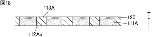
- FIG. 18 is a schematic cross-sectional view showing an example of the process of forming the first unsintered ceramic restraint part in an example of the method for manufacturing an ion generator according to Embodiment 2 of the present invention.
- FIG. 19 is a schematic cross-sectional view showing an example of a step of preparing a second unsintered ceramic layer in an example of the method for manufacturing an ion generator according to Embodiment 2 of the present invention.
- FIG. 20 is a schematic cross-sectional view showing an example of a step of forming a through hole in the second unsintered ceramic layer in an example of the method for manufacturing an ion generator according to Embodiment 2 of the present invention.
- FIG. 21 is a schematic cross-sectional view showing an example of a step of forming a second unsintered ceramic restraint part in an example of the method for manufacturing an ion generator according to Embodiment 2 of the present invention.
- FIG. 22 is a schematic cross-sectional view showing an example of a step of preparing a third unsintered ceramic restraint part in an example of the method for manufacturing an ion generator according to Embodiment 2 of the present invention.
- FIG. 23 is a schematic cross-sectional view showing an example of the step of forming a through hole in the third unsintered ceramic restraint part in an example of the method for manufacturing an ion generator according to Embodiment 2 of the present invention.
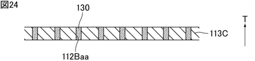
- FIG. 24 is a schematic cross-sectional view showing an example of a step of forming an unsintered current collecting electrode layer in an example of the method for manufacturing an ion generator according to Embodiment 2 of the present invention.
- FIG. 23 is a schematic cross-sectional view showing an example of the step of forming a through hole in the third unsintered ceramic restraint part in an example of the method for manufacturing an ion generator according to Embodiment 2 of the present invention.
- FIG. 24 is a schematic cross-sectional
- FIG. 25 is a schematic cross-sectional view showing an example of a step of partially removing the third unsintered ceramic restraint part in an example of the method for manufacturing an ion generator according to Embodiment 2 of the present invention.
- FIG. 26 is a schematic cross-sectional view showing an example of a step of preparing a third unsintered ceramic layer in an example of the method for manufacturing an ion generator according to Embodiment 2 of the present invention.
- FIG. 27 is a schematic cross-sectional view showing an example of a step of forming a through hole in the third unsintered ceramic layer in an example of the method for manufacturing an ion generator according to Embodiment 2 of the present invention.
- FIG. 28 shows an example of a step of forming a third unsintered ceramic restraining portion and an unsintered current collecting electrode layer on the third unsintered ceramic layer in an example of the method for manufacturing an ion generator according to Embodiment 2 of the present invention.
- FIG. FIG. 29 is a schematic cross-sectional view showing an example of a step of preparing a fourth unsintered ceramic layer in an example of the method for manufacturing an ion generator according to Embodiment 2 of the present invention.
- FIG. 30 is a schematic cross-sectional view showing an example of a step of forming a through hole in the fourth unsintered ceramic layer in an example of the method for manufacturing an ion generator according to Embodiment 2 of the present invention.
- FIG. 29 is a schematic cross-sectional view showing an example of a step of forming a through hole in the fourth unsintered ceramic layer in an example of the method for manufacturing an ion generator according to Embodiment 2 of the present invention.
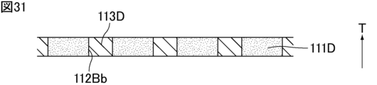
- FIG. 31 is a schematic cross-sectional view showing an example of the process of forming the fourth unsintered ceramic restraint part in an example of the method for manufacturing an ion generator according to Embodiment 2 of the present invention.
- FIG. 32 is a schematic cross-sectional view showing an example of a step of preparing a first unsintered ceramic constraining layer in an example of the method for manufacturing an ion generator according to Embodiment 2 of the present invention.
- FIG. 33 is a schematic cross-sectional view showing an example of a step of preparing a second unsintered ceramic constraining layer in an example of the method for manufacturing an ion generator according to Embodiment 2 of the present invention.
- FIG. 32 is a schematic cross-sectional view showing an example of a step of preparing a first unsintered ceramic constraining layer in an example of the method for manufacturing an ion generator according to Embodiment 2 of the present invention.
- FIG. 33 is a schematic cross-sectional view showing an example of a step
- FIG. 34 is a schematic cross-sectional view showing an example of a step of preparing a third unsintered ceramic constraining layer in an example of the method for manufacturing an ion generator according to Embodiment 2 of the present invention.
- FIG. 35 is a schematic cross-sectional view showing an example of a step of preparing a fourth unsintered ceramic constraining layer in an example of the method for manufacturing an ion generator according to Embodiment 2 of the present invention.
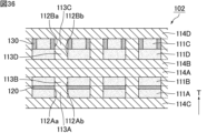
- FIG. 36 is a schematic cross-sectional view showing an example of a process for manufacturing a composite laminate in an example of the method for manufacturing an ion generator according to Embodiment 2 of the present invention.
- FIG. 37 is a schematic cross-sectional view showing a modification of the ion generator of Embodiment 2 of the present invention.
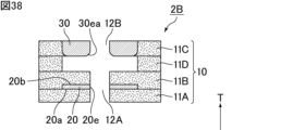
- FIG. 38 is a schematic cross-sectional view showing another modification of the ion generator of Embodiment 2 of the present invention.
- the ion generator of the present invention the discharge unit for the ion generator of the present invention, and the manufacturing method of the ion generator of the present invention will be explained.
- the present invention is not limited to the following configuration, and may be modified as appropriate without departing from the gist of the present invention.
- the present invention also includes a combination of a plurality of individual preferred configurations described below.
- the ion generator of the present invention includes an insulating substrate including a plurality of ceramic layers laminated in the thickness direction, a discharge electrode provided on the insulated substrate, and a space between the discharge electrode and the discharge electrode at a position facing the discharge electrode in the thickness direction.
- the plurality of ceramic layers include at least a first ceramic layer and a second ceramic layer adjacent to the first ceramic layer in the thickness direction
- the insulating substrate includes: A plurality of first through holes are provided that penetrate at least the first ceramic layer and the second ceramic layer in the thickness direction, and the discharge electrode is provided between the first ceramic layer and the second ceramic layer in the thickness direction, and , is exposed from the inner wall surface of the plurality of first through holes.
- Embodiment 1 of the present invention will be explained.
- the discharge electrode is provided on the insulated substrate, whereas the current collection electrode is not provided on the insulated substrate. More specifically, the ion generator of Embodiment 1 of the present invention includes a discharge unit having a discharge electrode provided on an insulated substrate, and a current collection unit having a current collection electrode not provided on the insulated substrate. We are prepared. A discharge unit for such an ion generator is also an aspect of the invention.
- a discharge unit for an ion generator includes an insulating substrate including a plurality of ceramic layers laminated in the thickness direction, and a discharge electrode provided on the insulating substrate, wherein the plurality of ceramic layers is a first ceramic layer. and a second ceramic layer adjacent to the first ceramic layer in the thickness direction, and the insulating substrate has a plurality of first through holes that penetrate at least the first ceramic layer and the second ceramic layer in the thickness direction.
- the discharge electrode is provided between the first ceramic layer and the second ceramic layer in the thickness direction, and is exposed from the inner wall surface of the plurality of first through holes.
- FIG. 1 is a schematic cross-sectional view showing an example of an ion generator according to Embodiment 1 of the present invention.
- FIG. 2 is a schematic plan view showing an example of the ion generator shown in FIG. 1 viewed from the discharge electrode side in the thickness direction. Note that, in order to focus on the discharge electrode, FIG. 2 shows the ion generator shown in FIG. 1 seen through from the discharge electrode side in the thickness direction.
- the ion generator 1 shown in FIG. 1 includes a discharge unit U1 and a current collection unit U2.
- the current collection unit U2 is attached to the discharge unit U1.
- one of the discharge unit U1 and the current collection unit U2 may be provided with a positioning pin, and the other may be provided with a positioning hole. By fitting these positioning pins and holes, the current collection unit U2 is attached to the discharge unit U1.
- the discharge unit U1 has an insulating substrate 10 and a discharge electrode (emitter electrode) 20.
- the insulating substrate 10 includes a plurality of ceramic layers stacked in the thickness direction T. More specifically, as shown in FIG. 1, the plurality of ceramic layers constituting the insulating substrate 10 include at least a first ceramic layer 11A and a second ceramic layer 11B stacked in the thickness direction T. I'm here.
- the second ceramic layer 11B is adjacent to the first ceramic layer 11A in the thickness direction T.
- the second ceramic layer 11B is adjacent to the first ceramic layer 11A on the discharge electrode 20 side in the thickness direction T.
- At least one ceramic layer may be further provided on the opposite side of the first ceramic layer 11A from the discharge electrode 20 so as to be adjacent to the first ceramic layer 11A in the thickness direction T.
- At least one ceramic layer may be further provided on the opposite side of the second ceramic layer 11B from the discharge electrode 20 so as to be adjacent to the second ceramic layer 11B in the thickness direction T.
- the plurality of ceramic layers constituting the insulating substrate 10 further include a ceramic layer 11X in addition to the first ceramic layer 11A and the second ceramic layer 11B.
- the ceramic layer 11X is provided adjacent to the second ceramic layer 11B in the thickness direction T on the opposite side of the second ceramic layer 11B from the discharge electrode 20.
- the constituent material of the ceramic layer is preferably a low-temperature sintered ceramic material.
- the ceramic layers such as the first ceramic layer 11A constituting the insulating substrate 10 are, for example, layers made of a ceramic material obtained by laminating and sintering green sheets.
- materials constituting such a ceramic layer include alumina, aluminum nitride, and low temperature sintered ceramic (LTCC) materials. In particular, low temperature sintered ceramic materials are preferred.
- a low-temperature sintered ceramic material means a ceramic material that can be sintered at a firing temperature of 1000° C. or lower. Low temperature sintered ceramic materials can be co-fired with copper, silver, etc.
- low-temperature sintered ceramic materials include glass composite low-temperature sintered ceramic materials containing ceramic materials such as quartz, alumina, and forsterite and borosilicate glass, and ZnO--MgO--Al 2 O 3 --SiO 2- based crystals.
- Non-crystalline glass-based low-temperature sintered ceramic materials including ceramicized glass, BaO-Al 2 O 3 -SiO 2- based ceramic materials, Al 2 O 3 -CaO-SiO 2 -MgO-B 2 O 3 -based ceramic materials, etc. Examples include glass-based low-temperature sintered ceramic materials.
- the insulating substrate 10 is provided with a plurality of first through holes 12A that penetrate at least the first ceramic layer 11A and the second ceramic layer 11B in the thickness direction T.
- a plurality of first through holes 12A are provided so as to penetrate in the thickness direction T through the first ceramic layer 11A and the second ceramic layer 11B.
- Each of the plurality of first through holes 12A functions as an intake port.
- the cross-sectional shapes of the plurality of first through-holes 12A when viewed from the direction perpendicular to the thickness direction T are the same. Note that the cross-sectional shapes of the plurality of first through holes 12A may be different from each other, or may be partially different.
- the cross-sectional shape of the plurality of first through-holes 12A when viewed from the direction perpendicular to the thickness direction T may independently be a tapered shape different from that in FIG. 1.
- planar shapes of the plurality of first through holes 12A when viewed from the thickness direction T are preferably the same. Note that the planar shapes of the plurality of first through holes 12A may be different from each other, or may be partially different.
- the planar shape of the plurality of first through holes 12A when viewed from the thickness direction T includes a circular shape, an elliptical shape, a polygonal shape, etc. as shown in FIG.
- the plurality of first through holes 12A are preferably arranged regularly. Note that the plurality of first through holes 12A may be arranged randomly.
- the intervals between the plurality of first through holes 12A are preferably the same. Note that the intervals between the plurality of first through holes 12A may be different from each other, or may be different in some parts.
- the discharge electrode 20 is provided on the insulating substrate 10. More specifically, as shown in FIG. 1, the discharge electrode 20 is provided between the first ceramic layer 11A and the second ceramic layer 11B in the thickness direction T.
- the discharge electrode 20 has a first main surface 20a and a second main surface 20b facing each other in the thickness direction T, and in the example shown in FIG.
- the second ceramic layer 11B is in contact with the second main surface 20b of the discharge electrode 20.
- the entire first main surface 20a of the discharge electrode 20 is not exposed from the first ceramic layer 11A. Note that a portion of the first main surface 20a of the discharge electrode 20 may be exposed from the first ceramic layer 11A.
- the entire second main surface 20b of the discharge electrode 20 is not exposed from the second ceramic layer 11B. Note that a part of the second main surface 20b of the discharge electrode 20 may be exposed from the second ceramic layer 11B.
- the discharge electrode 20 is provided between the first ceramic layer 11A and the second ceramic layer 11B in the thickness direction T, the main surface of the insulating substrate 10 (for example, the opposite side of the discharge electrode 20 in the second ceramic layer 11B)
- the discharge electrode 20 is arranged with high precision with respect to the side main surface 11Ba).
- the discharge electrode 20 is formed in a state in which it is restrained by the first unsintered ceramic restraint part 113A or the second unsintered ceramic restraint part 113B ( (See Figure 10).
- the first unsintered ceramic restraint part 113A and the second unsintered ceramic restraint part 113B are not sintered during firing, that is, the first unsintered ceramic restraint part 113A and the second unsintered ceramic restraint part 113B does not shrink during firing. Therefore, in the obtained ion generator 1, undesired deformation of the insulating substrate 10 and the discharge electrode 20 is suppressed.
- the discharge electrode 20 is accurately arranged on the main surface of the insulating substrate 10 (for example, the main surface 11Ba of the second ceramic layer 11B on the opposite side to the discharge electrode 20).
- the discharge electrode preferably has a flat plate shape extending in a direction perpendicular to the thickness direction.
- the discharge electrode 20 preferably has a flat plate shape extending in a direction perpendicular to the thickness direction T. In this case, it becomes easy to form the discharge electrode 20, and it also becomes easy to arrange the discharge electrode 20 with high precision.
- the flat plate shape means a shape in which the dimension in the thickness direction is 1/10 or less of the minimum dimension in the direction orthogonal to the thickness direction.
- the constituent material of the discharge electrode 20 various conductive materials can be mentioned.
- the conductive material constituting the discharge electrode 20 may include copper, silver, or at least one of these metals. Examples include alloys that In the discharge electrode 20, the above-mentioned conductive material may be coated with a corrosion-resistant metal material such as gold, chromium, platinum, nickel, tungsten, or molybdenum by plating, sputtering, or the like.
- the discharge electrode 20 is exposed from the inner wall surface of the plurality of first through holes 12A. More specifically, as shown in FIG. 1, the ends of the discharge electrode 20 in the direction perpendicular to the thickness direction T are exposed from the inner wall surfaces of the plurality of first through holes 12A as a plurality of exposed portions 20e. .
- the plurality of exposed parts 20e of the discharge electrode 20 function as a plurality of discharge parts, a configuration having a plurality of discharge parts can be realized without providing a plurality of discharge electrodes 20. Therefore, in the ion generator 1, the amount of ions generated can be increased by having a configuration including a plurality of discharge parts.
- the exposed portion 20e of the discharge electrode 20, which functions as a discharge portion is provided so as to be in contact with the first through hole 12A, which functions as an intake port. Ions are efficiently released.
- the discharge electrode 20 is exposed from the inner wall surface of a plurality of first through holes 12A among all the first through holes 12A provided in the insulating substrate 10; It is particularly preferable that it be exposed from the inner wall surface of the first through hole 12A.
- the discharge electrode is preferably exposed over the entire circumference of the inner wall surface of at least one first through hole.
- the discharge electrode 20 is preferably exposed over the entire circumference of the inner wall surface of at least one first through hole 12A.
- the discharge electrode 20 is exposed over the entire circumference of the inner wall surface of the plurality of first through holes 12A. In this case, the amount of ions generated by the discharge electrode 20 tends to increase.
- the discharge electrode 20 only needs to be exposed from the inner wall surface of the plurality of first through holes 12A among all the first through holes 12A provided in the insulating substrate 10.
- the discharge electrode 20 is exposed over the entire circumference of the inner wall surface of at least one first through hole 12A, and all the first through holes It is more preferable that the discharge electrode 20 is exposed over the entire circumference of the inner wall surface 12A.
- the discharge electrode 20 and the first through hole 12A do not overlap when viewed from the thickness direction T.
- the end (outer edge) of the discharge electrode 20 on the opposite side to the first through hole 12A is Preferably, it is not exposed from the first ceramic layer 11A and the second ceramic layer 11B.
- the end of the discharge electrode 20 opposite to the first through hole 12A may be covered with at least one of the first ceramic layer 11A and the second ceramic layer 11B, or may be covered with an insulating member other than the ceramic layer. It may be sealed.
- the discharge electrode 20 may be divided into a plurality of parts within a plane along a direction perpendicular to the thickness direction T.
- the discharge electrode 20 When the discharge electrode 20 is divided into a plurality of parts, it is preferable that all the divided discharge electrodes 20 are exposed from the inner wall surface of the plurality of first through holes 12A.
- the discharge electrode 20 When the discharge electrode 20 is divided into a plurality of parts, the plurality of divided discharge electrodes 20 may be connected to each other via a conductive part such as wiring.
- the cross-sectional shapes of the plurality of divided discharge electrodes 20 when viewed from a direction perpendicular to the thickness direction T are the same. Note that the cross-sectional shapes of the plurality of divided discharge electrodes 20 may be different from each other, or may be partially different.
- the planar shape of the plurality of divided discharge electrodes 20 when viewed from the thickness direction T is the same. Note that the planar shapes of the plurality of divided discharge electrodes 20 may be different from each other, or may be partially different.
- one main surface of the insulating substrate is located at a higher position in the thickness direction than the main surface of the second ceramic layer, in addition to the main surface of the second ceramic layer on the opposite side to the discharge electrode. It may include the main surface of the ceramic layer.
- one main surface 10a of the insulating substrate 10 is thicker than the main surface 11Ba of the second ceramic layer 11B in addition to the main surface 11Ba of the second ceramic layer 11B opposite to the discharge electrode 20.
- the main surface 11Xa of the ceramic layer 11X located at a high position in T may be included.
- the main surface 11Xa of the ceramic layer 11X in the discharge unit U1 can be used as a reference surface for attaching the current collection unit U2.
- one ceramic layer 11X is provided on the opposite side of the second ceramic layer 11B from the discharge electrode 20 so as to be adjacent to the second ceramic layer 11B in the thickness direction T.
- Two or more ceramic layers may be provided.
- the dimension in the thickness direction T of the ceramic layer 11X may be the same as or different from the dimension in the thickness direction T of the first ceramic layer 11A and the second ceramic layer 11B.
- the ceramic layer 11X may not be provided.
- the main surface 11Ba of the second ceramic layer 11B in the discharge unit U1 can be used as a reference surface for attaching the current collecting unit U2.
- the current collecting unit U2 has a current collecting electrode 30 (collector electrode).
- the current collecting electrode 30 is provided at a position facing the discharge electrode 20 in the thickness direction T, with a space separated from the discharge electrode 20. That is, the current collecting electrode 30 is exposed in a common space between the discharge electrode 20 and the current collecting electrode 30.
- the exposed location of the current collecting electrode 30 is not particularly limited as long as it is exposed in a common space between the discharge electrode 20 and the current collecting electrode 30.
- the discharge electrode 20 is exposed from the inner wall surface of the plurality of first through holes 12A, so that it is exposed in the common space between the discharge electrode 20 and the current collecting electrode 30. ing.
- the ion generator 1 since the discharge electrode 20 and the current collection electrode 30 are exposed in a common space as shown in FIG. 1, ion generation by corona discharge can be realized.
- the ion generator 1 not only generates ions, but also functions as an ion wind generator that generates ion wind. More specifically, first, when a positive or negative high voltage is applied to the discharge electrode 20 by a high voltage power supply (not shown) connected to the discharge electrode 20, the discharge electrode 20 and the current collecting electrode 30 are connected to each other. A strong electric field is formed during this period, and a large potential gradient is generated around the exposed portion 20e of the discharge electrode 20.
- ions generated by corona discharge are generated by a potential difference between a discharge electrode 20 connected to a high voltage power source (not shown) and a current collecting electrode 30 connected to a ground (not shown). Drift by. At this time, when the surrounding air is drawn in by the ion drift, an air flow called ion wind is generated. In this way, the ion generator 1 not only generates ions, but also functions as an ion wind generator that generates ion wind. When the ion generator 1 functions as an ion wind generator, the amount of ion wind increases as the amount of generated ions increases due to the configuration having a plurality of discharge parts.
- the current collecting electrode 30 is preferably provided with a plurality of third through holes 12C that penetrate in the thickness direction T.
- Each of the plurality of third through holes 12C functions as an exhaust port.
- Examples of the current collecting electrode 30 provided with the plurality of third through holes 12C include a punched mesh containing a conductive material.
- Examples of the conductive material constituting such a punched mesh include stainless steel, aluminum, titanium, and copper.
- the above-mentioned conductive material may be coated with a metal material having corrosion resistance such as gold, chromium, platinum, nickel, tungsten, molybdenum, etc. by a plating method, a sputtering method, or the like.
- the plurality of third through holes 12C communicate with the plurality of first through holes 12A.
- an air flow path is formed.
- the plurality of third through holes 12C communicate with the plurality of first through holes 12A via the space between the plurality of first through holes 12A and the plurality of third through holes 12C. ing. More specifically, the plurality of first through holes 12A and the plurality of third through holes 12C communicate with each other via a common space extending in a direction perpendicular to the thickness direction T.
- the cross-sectional shapes of the plurality of third through holes 12C when viewed from the direction perpendicular to the thickness direction T are preferably the same. Note that the cross-sectional shapes of the plurality of third through holes 12C may be different from each other, or may be partially different.
- the cross-sectional shape of the plurality of third through holes 12C when viewed from the direction perpendicular to the thickness direction T may be independently tapered, which is different from that in FIG. 1.
- planar shapes of the plurality of third through holes 12C when viewed from the thickness direction T are the same. Note that the planar shapes of the plurality of third through holes 12C may be different from each other, or may be partially different.
- the planar shape of the plurality of third through holes 12C when viewed from the thickness direction T includes a circular shape, an elliptical shape, a polygonal shape, etc.
- the plurality of third through holes 12C are arranged regularly. Note that the plurality of third through holes 12C may be randomly arranged.
- intervals between the plurality of third through holes 12C are the same. Note that the intervals between the plurality of third through holes 12C may be different from each other, or may be different in some parts.
- the ion generator 1 functions as an ion wind generator, the speed of the ion wind is likely to increase.
- At least one of the plurality of first through holes 12A and the plurality of third through holes 12C does not need to overlap when viewed from the thickness direction T.
- the center of the first through hole 12A and the center of the third through hole 12C when viewed from the thickness direction are the same. It is preferable that the
- the center of the first through hole 12A and the center of the third through hole 12C when viewed from the thickness direction are , do not have to match.
- the number of first through holes 12A and the number of third through holes 12C are preferably the same. In this case, there will be a plurality of pairs consisting of one first through hole 12A and one third through hole 12C, but in all the pairs, the first through hole 12A and the third through hole 12C are It is preferable that they overlap when viewed from the thickness direction T. Note that in some sets, the first through hole 12A and the third through hole 12C may overlap when viewed from the thickness direction T.
- first through holes 12A and the number of third through holes 12C may be different.
- the current collecting electrode has a proximate exposed portion exposed to space in the lower half region on the discharge electrode side in the thickness direction; It is preferable that twice the minimum radius of curvature is larger than the dimension in the thickness direction of the discharge electrode.
- the current collecting electrode 30 preferably has a proximate exposed portion 30ea exposed to space in the lower half region R on the discharge electrode 20 side in the thickness direction T.
- the lower half region R on the discharge electrode 20 side in the thickness direction T is the region of the current collecting electrode 30 on the discharge electrode 20 side, as shown by the region surrounded by the dotted line in FIG. This is a region whose dimension in the thickness direction T corresponds to half of the dimension in the thickness direction T of the current collecting electrode 30 . That is, the proximal exposed portion 30ea of the current collecting electrode 30 is located near the discharge electrode 20 in the thickness direction T, and is exposed in the space separating the discharge electrode 20 and the current collecting electrode 30.
- the corners be rounded, for example.
- twice the minimum radius of curvature of the proximal exposed portion 30ea of the current collecting electrode 30 is preferably larger than the dimension in the thickness direction T of the discharge electrode 20. In this case, it can be said that the adjacent exposed portion 30ea of the current collecting electrode 30 does not have a sharper portion than the exposed portion 20e of the discharge electrode 20.
- the adjacent exposed portion 30ea of the current collecting electrode 30 does not have a sharper portion than the exposed portion 20e of the discharging electrode 20, even if a strong electric field is formed between the discharging electrode 20 and the current collecting electrode 30, , electric field concentration does not occur at the proximal exposed portion 30ea of the current collecting electrode 30, and as a result, corona discharge is less likely to occur from the proximal exposed portion 30ea of the current collecting electrode 30.
- proximal exposed portion 30ea of the current collecting electrode 30 has a sharper portion than the exposed portion 20e of the discharging electrode 20, a corona discharge with a polarity opposite to that of the discharging electrode 20 is generated from the proximate exposed portion 30ea of the current collecting electrode 30. becomes more likely to occur.
- the current collecting electrode 30 has an exposed portion exposed to space also in the upper half region on the opposite side to the discharge electrode 20 in the thickness direction T, that is, in a region other than the region R. .
- Corona discharge is less likely to occur in the exposed portions of the current collecting electrode 30 that are present in areas other than the area R, even if sharp portions are present. Therefore, as shown in FIG. 1, twice the minimum radius of curvature at the exposed portion of the current collecting electrode 30 other than the region R, for example, at the corner of the current collecting electrode 30 on the opposite side from the discharge electrode 20, is It may be smaller than the dimension in the thickness direction T of the discharge electrode 20.
- the size of the current collecting electrode in the thickness direction is preferably larger than the size of the discharge electrode in the thickness direction.
- the size of the current collecting electrode 30 in the thickness direction T is preferably larger than the size of the discharge electrode 20 in the thickness direction T. Further, the dimension of the exposed portion of the current collecting electrode 30 in the thickness direction T is preferably larger than the dimension of the exposed portion of the discharge electrode 20 in the thickness direction T.
- the dimension in the thickness direction T of the current collecting electrode 30 is smaller than the dimension in the thickness direction T of the discharge electrode 20. Since the corona discharge of the opposite polarity to the discharge electrode is suppressed by the current collecting electrode 30, the ions of the opposite polarity generated from the discharge electrode 20 and the current collecting electrode 30 are neutralized, and as a result, the ions This suppresses a decrease in the amount of generation. Further, when the ion generator 1 functions as an ion wind generator, the amount of ion wind increases.
- the ion generator 1 may further include a spacer 40 provided between the discharge unit U1 and the current collection unit U2 in the thickness direction T. Thereby, the space between the discharge unit U1 and the current collection unit U2, that is, the space between the discharge electrode 20 and the current collection electrode 30, is easily secured.
- Examples of the constituent material of the spacer 40 include insulating materials such as resin, ceramic, and glass.
- the spacer 40 may be integrated with the current collecting unit U2.
- the current collecting electrode 30 may be provided on the spacer 40.
- the method for manufacturing an ion generator of the present invention includes an insulating substrate including a plurality of ceramic layers laminated in the thickness direction, a discharge electrode provided on the insulated substrate, and a discharge electrode at a position facing the discharge electrode in the thickness direction.
- a method for manufacturing an ion generator comprising: a first unsintered ceramic layer included in a plurality of unsintered ceramic layers to be a plurality of ceramic layers; a step of preparing, a step of forming an unsintered discharge electrode layer to become a discharge electrode on one main surface of the first unsintered ceramic layer, and a step of penetrating the first unsintered ceramic layer in the thickness direction.
- FIG. 3 is a schematic cross-sectional view showing an example of a step of preparing a first unsintered ceramic layer in an example of the method for manufacturing an ion generator according to Embodiment 1 of the present invention.
- a first unsintered ceramic layer 111A is prepared.
- the first unsintered ceramic layer 111A is to become the first ceramic layer 11A among the plurality of ceramic layers included in the insulating substrate 10 in the ion generator 1 obtained later.
- the first unsintered ceramic layer 111A for example, a ceramic green sheet containing an unsintered ceramic material is prepared.
- Such a ceramic green sheet is produced, for example, by the following method.
- a ceramic slurry is prepared by mixing a ceramic material such as a low-temperature sintered ceramic material, a binder, a solvent, etc. in a predetermined ratio.
- additives such as a dispersant and a plasticizer may be added.
- a ceramic green sheet is produced by forming the obtained ceramic slurry into a sheet shape using a doctor blade method or the like.
- FIG. 4 is a schematic cross-sectional view showing an example of a step of forming an unsintered discharge electrode layer in an example of the method for manufacturing an ion generator according to Embodiment 1 of the present invention.
- an unsintered discharge electrode layer 120 is formed on one main surface of the first unsintered ceramic layer 111A.
- the unsintered discharge electrode layer 120 is to become the discharge electrode 20 in the ion generator 1 obtained later.
- the unsintered discharge electrode layer 120 for example, when using a low-temperature sintered ceramic material as the ceramic material included in the unsintered ceramic layer, a conductive paste containing a conductive material such as copper or silver is used. It is coated on one main surface of the first unsintered ceramic layer 111A using a screen printing method or the like.
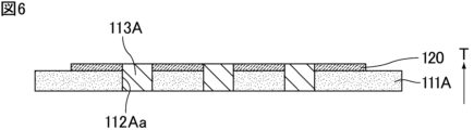
- FIG. 5 is a schematic cross-sectional view showing an example of a step of forming a through hole in the first unsintered ceramic layer in an example of the method for manufacturing an ion generator according to the first embodiment of the present invention.
- a plurality of through holes 112Aa penetrating in the thickness direction T are formed in the first unsintered ceramic layer 111A.
- a plurality of through holes 112Aa penetrating in the thickness direction T are formed in the first unsintered ceramic layer 111A on the main surface of which the unsintered discharge electrode layer 120 is formed.
- Each of the plurality of through holes 112Aa should become a part of the first through hole 12A in the ion generator 1 obtained later.
- the first unsintered ceramic layer 111A may be irradiated with a laser beam or punched out, for example.
- the "step of forming a through hole in the first unsintered ceramic layer” (see FIG. 5) is performed. ) has been described, but these steps may be performed in the reverse order.
- an unsintered discharge electrode is placed on one main surface of the first unsintered ceramic layer 111A in which the plurality of through holes 112Aa are formed.
- a layer 120 may also be formed.
- FIG. 6 is a schematic cross-sectional view showing an example of the process of forming the first unsintered ceramic restraint part in an example of the method for manufacturing the ion generator according to Embodiment 1 of the present invention.
- a first unsintered ceramic restraining portion 113A is formed inside each of the plurality of through holes 112Aa formed in the first unsintered ceramic layer 111A.
- the first unsintered ceramic restraining portion 113A is not sintered at a temperature at which unsintered ceramic layers such as the first unsintered ceramic layer 111A are sintered. That is, the sintering temperature of the first unsintered ceramic constraint portion 113A is higher than the sintering temperature of the unsintered ceramic layer.
- a ceramic slurry containing a ceramic material that does not sinter at a temperature at which the ceramic material included in the unsintered ceramic layer sinters is applied to each of the plurality of through holes 112Aa. It may be filled inside.
- a ceramic green sheet may be produced by forming a similar ceramic slurry into a sheet shape, and then the ceramic green sheet may be placed inside each of the plurality of through holes 112Aa.
- the ceramic material contained in the first unsintered ceramic restraining portion 113A may be, for example, alumina, zirconium oxide, aluminum nitride, boron nitride. , mullite, magnesium oxide, silicon carbide, etc. can be used. Among them, alumina is preferred.
- FIG. 7 is a schematic cross-sectional view showing an example of a step of preparing a second unsintered ceramic layer in an example of the method for manufacturing an ion generator according to Embodiment 1 of the present invention.
- a second unsintered ceramic layer 111B is prepared.
- the second unsintered ceramic layer 111B is to become the second ceramic layer 11B among the plurality of ceramic layers included in the insulating substrate 10 in the ion generator 1 obtained later.
- the second unsintered ceramic layer 111B is prepared in the same manner as the first unsintered ceramic layer 111A, for example.
- FIG. 8 is a schematic cross-sectional view showing an example of the step of forming a through hole in the second unsintered ceramic layer in an example of the method for manufacturing the ion generator according to the first embodiment of the present invention.
- a plurality of through holes 112Ab penetrating in the thickness direction T are formed in the second unsintered ceramic layer 111B.
- Each of the plurality of through holes 112Ab should become a part of the first through hole 12A in the ion generator 1 obtained later.
- the plurality of through holes 112Ab are formed in the second unsintered ceramic layer 111B, for example, in the same manner as the plurality of through holes 112Aa.
- FIG. 9 is a schematic cross-sectional view showing an example of the process of forming the second unsintered ceramic restraint part in an example of the method for manufacturing the ion generator according to the first embodiment of the present invention.
- a second unsintered ceramic restraining portion 113B is formed inside each of the plurality of through holes 112Ab formed in the second unsintered ceramic layer 111B.
- the second unsintered ceramic restraining portion 113B is not sintered at a temperature at which unsintered ceramic layers such as the first unsintered ceramic layer 111A are sintered. That is, the sintering temperature of the second unsintered ceramic constraint portion 113B is higher than the sintering temperature of the unsintered ceramic layer.
- the second unsintered ceramic restraint part 113B is formed inside each of the plurality of through holes 112Ab, for example, in the same manner as the first unsintered ceramic restraint part 113A.
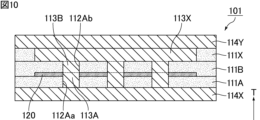
- FIG. 10 is a schematic cross-sectional view showing an example of a process for manufacturing a composite laminate in an example of the method for manufacturing an ion generator according to Embodiment 1 of the present invention.
- a first unsintered ceramic layer 111A is provided with an unsintered discharge electrode layer 120 and a first unsintered ceramic restraint part 113A, and a second unsintered ceramic restraint part 113B is provided.
- the composite laminate 101 is produced by laminating the second unsintered ceramic layer 111B in the thickness direction T.
- the unsintered ceramic restraint part 113B is formed using the same method as the second unsintered ceramic layer 111B provided with the second unsintered ceramic restraint part 113B.
- An unsintered ceramic layer 111X provided with an unsintered ceramic layer 113X is prepared in advance.
- a composite laminate 101 is produced.
- an unsintered A bound ceramic constraining layer 114X may be further laminated.
- an unsintered ceramic restraining layer 114Y may be further laminated on the side opposite to the unsintered discharge electrode layer 120 with respect to the unsintered ceramic layer 111X provided with the unsintered ceramic restraining portion 113X.
- the ceramic layer 111A and the second unsintered ceramic layer 111B are laminated in the thickness direction T with the unsintered discharge electrode layer 120 interposed therebetween.
- the plurality of through-holes 112Aa in which the first unsintered ceramic restraint parts 113A are formed and the plurality of through-holes 112Ab in which the second unsintered ceramic restraint parts 113B are formed respectively.
- a composite laminate 101 is manufactured in which an unsintered discharge electrode layer 120 is provided so as to reach the inner wall surfaces of a plurality of composite through holes formed in communication in the thickness direction T.
- the composite laminate 101 shown in FIG. 10 is fired at a temperature at which the green ceramic layer is sintered. More specifically, the temperature is such that the unsintered ceramic layers such as the first unsintered ceramic layer 111A are sintered, and the unsintered ceramic restraint parts such as the first unsintered ceramic restraint part 113A are sintered. The composite laminate 101 is fired at a temperature that does not exceed 100 degrees.
- the first unsintered ceramic layer 111A, the second unsintered ceramic layer 111B, and the unsintered ceramic layer 111X become the first ceramic layer 11A and the second ceramic layer, respectively. 11B and a ceramic layer 11X.
- the unsintered discharge electrode layer 120 becomes the discharge electrode 20.
- the first unsintered ceramic restraint part 113A, the second unsintered ceramic restraint part 113B, and the unsintered ceramic restraint part 113X are made non-sintered without being sintered. It becomes a knot.
- the unsintered ceramic restraining portion that is not sintered at the firing temperature does not shrink. Therefore, undesirable deformation of the obtained insulating substrate 10 and discharge electrode 20 can be suppressed. As a result, the discharge electrode 20 can be arranged with high precision on the one principal surface 10a of the insulating substrate 10.
- the non-sintered portion is brittle, the non-sintered portion can be removed after firing the composite laminate 101.
- the plurality of through holes 112Aa and the plurality of through holes 112Ab are communicated one by one in the thickness direction T to become a plurality of first through holes 12A.
- Examples of methods for removing the non-sintered portion include wet blasting, sandblasting, brushing, and ultrasonic cleaning.
- the ion generator 1 shown in FIGS. 1 and 2 is manufactured by attaching the current collecting unit U2 to the discharge unit U1 via the spacer 40. .
- the current collecting electrode 30 constituting the current collecting unit U2 is assumed to be a punched mesh containing a conductive material, but the current collecting electrode 30 is a wire containing a conductive material. It may be a mesh, a printed circuit board on which a conductive pattern is arranged, a resin structure whose surface is plated with a metal pattern, or the like.
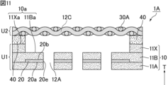
- FIG. 11 is a schematic cross-sectional view showing a modification of the ion generator of Embodiment 1 of the present invention.
- the current collecting electrode 30A that constitutes the current collecting unit U2 is a wire mesh.
- the gaps between the woven wires function as third through holes 12C.
- the conductive material constituting the wire mesh examples include stainless steel, aluminum, titanium, copper, and the like.
- the above-mentioned conductive material may be coated with a corrosion-resistant metal material such as gold, chromium, platinum, nickel, tungsten, molybdenum, etc. by plating, sputtering, or the like.
- the diameter of the wire constituting the wire mesh that is the current collecting electrode 30A is preferably larger than the dimension in the thickness direction T of the discharge electrode 20.
- the size of the current collecting electrode 30A in the thickness direction T is larger than the size of the discharge electrode 20 in the thickness direction T.
- FIG. 12 is a schematic cross-sectional view showing an example of an ion generator according to Embodiment 2 of the present invention.
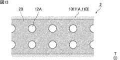
- FIG. 13 is a schematic plan view showing an example of the ion generator shown in FIG. 12 viewed from the discharge electrode side in the thickness direction. Note that, in order to focus on the discharge electrode, FIG. 13 shows the ion generator shown in FIG. 12 seen through from the discharge electrode side in the thickness direction.
- FIG. 14 is a schematic plan view showing an example of the state in which the ion generator shown in FIG. 12 is viewed from the current collecting electrode side in the thickness direction.
- the ion generator 2 shown in FIG. 12 includes an insulating substrate 10, a discharge electrode 20, and a current collection electrode 30.
- the insulating substrate 10 includes a plurality of ceramic layers stacked in the thickness direction T. More specifically, as shown in FIG. 12, the plurality of ceramic layers constituting the insulating substrate 10 include at least a first ceramic layer 11A and a second ceramic layer 11B stacked in the thickness direction T. I'm here.
- the second ceramic layer 11B is adjacent to the first ceramic layer 11A in the thickness direction T.
- the second ceramic layer 11B is adjacent to the first ceramic layer 11A on the collector electrode 30 side in the thickness direction T.
- At least one ceramic layer is further provided on the opposite side of the first ceramic layer 11A from the current collecting electrode 30 so as to be adjacent to the first ceramic layer 11A in the thickness direction T. Good too.
- At least one ceramic layer may be further provided on the current collecting electrode 30 side of the second ceramic layer 11B so as to be adjacent to the second ceramic layer 11B in the thickness direction T. .
- the insulating substrate 10 is provided with a plurality of first through holes 12A that penetrate at least the first ceramic layer 11A and the second ceramic layer 11B in the thickness direction T.
- a plurality of first through holes 12A are provided so as to penetrate in the thickness direction T through the first ceramic layer 11A and the second ceramic layer 11B.
- the discharge electrode 20 is provided on the insulating substrate 10. More specifically, as shown in FIG. 12, the discharge electrode 20 is provided between the first ceramic layer 11A and the second ceramic layer 11B in the thickness direction T.
- the discharge electrode 20 has a first main surface 20a and a second main surface 20b facing each other in the thickness direction T, and in the example shown in FIG.
- the second ceramic layer 11B is in contact with the second main surface 20b of the discharge electrode 20.
- the entire first main surface 20a of the discharge electrode 20 is not exposed from the first ceramic layer 11A. Note that a portion of the first main surface 20a of the discharge electrode 20 may be exposed from the first ceramic layer 11A.
- the entire second main surface 20b of the discharge electrode 20 is not exposed from the second ceramic layer 11B. Note that a part of the second main surface 20b of the discharge electrode 20 may be exposed from the second ceramic layer 11B.
- the discharge electrode 20 By providing the discharge electrode 20 between the first ceramic layer 11A and the second ceramic layer 11B in the thickness direction T, the main surface of the insulating substrate 10 (for example, the opposite side of the discharge electrode 20 in the first ceramic layer 11A)
- the discharge electrode 20 is arranged with high precision with respect to the main surface of the side.
- the discharge electrode 20 is formed in a state where it is restrained by the first unsintered ceramic restraint part 113A or the second unsintered ceramic restraint part 113B ( (See Figure 36).
- the first unsintered ceramic restraint part 113A and the second unsintered ceramic restraint part 113B are not sintered during firing, that is, the first unsintered ceramic restraint part 113A and the second unsintered ceramic restraint part 113B does not shrink during firing. Therefore, in the obtained ion generator 2, undesired deformation of the insulating substrate 10 and the discharge electrode 20 is suppressed.
- the discharge electrode 20 is accurately arranged on the main surface of the insulating substrate 10 (for example, the main surface on the opposite side to the discharge electrode 20 in the first ceramic layer 11A).
- the discharge electrode 20 is exposed from the inner wall surface of the plurality of first through holes 12A. More specifically, as shown in FIG. 12, the ends of the discharge electrode 20 in the direction perpendicular to the thickness direction T are exposed from the inner wall surfaces of the plurality of first through holes 12A as a plurality of exposed parts 20e. .
- the plurality of exposed parts 20e of the discharge electrode 20 function as a plurality of discharge parts, a configuration having a plurality of discharge parts can be realized without providing a plurality of discharge electrodes 20. Therefore, in the ion generator 2, the amount of ions generated can be increased by having a configuration including a plurality of discharge parts.
- the exposed portion 20e of the discharge electrode 20, which functions as a discharge portion is provided so as to be in contact with the first through hole 12A, which functions as an intake port, the Ions are efficiently released.
- the discharge electrode 20 is exposed from the inner wall surface of a plurality of first through holes 12A among all the first through holes 12A provided in the insulating substrate 10; It is particularly preferable that it be exposed from the inner wall surface of the first through hole 12A.
- the current collecting electrode 30 extends planarly in the thickness direction T.
- the current collecting electrode 30 is provided at a position facing the discharge electrode 20 in the thickness direction T, with a space between the discharge electrode 20 and the discharge electrode 20. That is, the current collecting electrode 30 is exposed in a common space between the discharge electrode 20 and the current collecting electrode 30.
- the discharge electrode 20 is exposed from the inner wall surface of the plurality of first through holes 12A, so that it is exposed in the common space between the discharge electrode 20 and the current collecting electrode 30. ing.
- the discharge electrode 20 and the current collection electrode 30 are exposed in a common space as shown in FIG. 12, ion generation by corona discharge can be realized. More specifically, similarly to the ion generator 1, by connecting a high voltage power source (not shown) to the discharge electrode 20 and connecting a ground (not shown) to the current collecting electrode 30, the discharge electrode 20 Corona discharge occurs from the exposed portion of the discharge electrode 20, and ions are generated in the air around the exposed portion of the discharge electrode 20.
- the ion generator 2 not only generates ions, but also functions as an ion wind generator that generates ion wind.
- the constituent material of the current collecting electrode 30 various conductive materials can be mentioned.
- the conductive material constituting the current collecting electrode 30 may include copper, silver, or at least one of these metals. Containing alloys, etc. can be mentioned.
- the above-mentioned conductive material may be coated with a metal material having corrosion resistance such as gold, chromium, platinum, nickel, tungsten, molybdenum, etc. by a plating method, a sputtering method, or the like.
- the constituent material of the current collecting electrode 30 may be the same as the constituent material of the discharge electrode 20, or may be different.
- the plurality of ceramic layers may further include a third ceramic layer provided on the opposite side of the discharge electrode with respect to the second ceramic layer in the thickness direction, and the current collecting electrode is Preferably, it is provided in the third ceramic layer and a portion thereof is exposed from the third ceramic layer.
- the plurality of ceramic layers constituting the insulating substrate 10 further include a third ceramic layer 11C provided on the opposite side of the discharge electrode 20 with respect to the second ceramic layer 11B in the thickness direction T. You can stay there.
- the current collecting electrode 30 is provided on the third ceramic layer 11C and a portion thereof is exposed from the third ceramic layer 11C.
- At least one ceramic layer may be further provided on the side of the third ceramic layer 11C opposite to the discharge electrode 20 so as to be adjacent to the third ceramic layer 11C in the thickness direction T. good.
- the plurality of ceramic layers constituting the insulating substrate 10 may further include a fourth ceramic layer 11D adjacent in the thickness direction T to the third ceramic layer 11C.
- the fourth ceramic layer 11D is adjacent to the third ceramic layer 11C on the discharge electrode 20 side in the thickness direction T.
- At least one ceramic layer may be further provided on the discharge electrode 20 side of the fourth ceramic layer 11D so as to be adjacent to the fourth ceramic layer 11D in the thickness direction T.
- the second ceramic layer 11B and the fourth ceramic layer 11D are connected in the thickness direction T in a predetermined region.
- the insulating substrate is provided with a plurality of second through holes that penetrate at least the third ceramic layer in the thickness direction.
- the insulating substrate 10 is preferably provided with a plurality of second through holes 12B that penetrate at least the third ceramic layer 11C in the thickness direction T.
- a plurality of second through holes 12B are provided so as to penetrate in the thickness direction T through the third ceramic layer 11C and the fourth ceramic layer 11D.
- Each of the plurality of second through holes 12B functions as an exhaust port.
- the plurality of second through holes 12B communicate with the plurality of first through holes 12A. As a result, an air flow path (ion wind flow path) is formed.
- the plurality of second through holes 12B connect to the plurality of first through holes 12A via a common space between the plurality of first through holes 12A and the plurality of second through holes 12B. It's communicating. More specifically, the plurality of first through holes 12A and the plurality of second through holes 12B communicate with each other via a common space extending in a direction perpendicular to the thickness direction T.
- the cross-sectional shapes of the plurality of second through-holes 12B when viewed from the direction perpendicular to the thickness direction T are the same. Note that the cross-sectional shapes of the plurality of second through holes 12B may be different from each other, or may be partially different.
- the cross-sectional shape of the plurality of second through-holes 12B when viewed from the direction perpendicular to the thickness direction T may independently be a tapered shape different from that in FIG. 12.
- planar shapes of the plurality of second through holes 12B when viewed from the thickness direction T are preferably the same. Note that the planar shapes of the plurality of second through holes 12B may be different from each other, or may be partially different.
- the planar shape of the plurality of second through holes 12B when viewed from the thickness direction T includes a circular shape, an elliptical shape, a polygonal shape, etc. as shown in FIG.
- the plurality of second through holes 12B are preferably arranged regularly. Note that the plurality of second through holes 12B may be randomly arranged.
- the intervals between the plurality of second through holes 12B are preferably the same. Note that the intervals between the plurality of second through holes 12B may be different from each other, or may be different in some parts.
- the current collecting electrode is exposed from the inner wall surface of the plurality of second through holes.
- the current collecting electrode 30 is preferably exposed from the inner wall surface of the plurality of second through holes 12B.
- the end of the current collecting electrode 30 in the direction perpendicular to the thickness direction T is exposed from the inner wall surface of the plurality of second through holes 12B.
- the current collecting electrode 30 is exposed from the inner wall surface of a plurality of second through holes 12B among all the second through holes 12B provided in the insulating substrate 10. Particularly preferably, it is exposed from the inner wall surface.
- the current collecting electrode when the current collecting electrode is exposed from the inner wall surface of the plurality of second through holes, the current collecting electrode is exposed over the entire circumference of the inner wall surface of at least one second through hole.
- the current collecting electrode is exposed over the entire circumference of the inner wall surface of at least one second through hole.
- the current collecting electrode 30 is preferably exposed over the entire circumference of the inner wall surface of at least one second through hole 12B.
- the current collecting electrode 30 is exposed over the entire circumference of the inner wall surface of the plurality of second through holes 12B.
- the current collecting electrode 30 is provided in a ring shape over the entire circumference of the inner wall surface of the plurality of second through holes 12B.
- the current collecting electrode 30 is preferably exposed from the inner wall surface of a plurality of second through holes 12B among all the second through holes 12B provided in the insulating substrate 10.
- the plurality of second through holes 12B in which the electrode 30 is exposed from the inner wall surface it is preferable that the current collecting electrode 30 is exposed over the entire circumference of the inner wall surface of at least one second through hole 12B. More preferably, the current collecting electrode 30 is exposed over the entire circumference of the inner wall surface of the second through hole 12B.
- the current collecting electrode 30 is exposed not only from the inner wall surface of the second through hole 12B but also from the main surface of the third ceramic layer 11C on the opposite side to the discharge electrode 20. Note that the current collecting electrode 30 does not need to be exposed from the main surface of the third ceramic layer 11C on the opposite side to the discharge electrode 20.
- the current collecting electrode 30 and the second through hole 12B do not overlap when viewed from the thickness direction T.
- a plurality of current collecting electrodes 30 are provided.
- the plurality of current collecting electrodes 30 may be connected to each other via a conductive part such as wiring.
- the cross-sectional shapes of the plurality of current collecting electrodes 30 are the same when viewed from a direction perpendicular to the thickness direction T. . Note that the cross-sectional shapes of the plurality of current collecting electrodes 30 may be different from each other, or may be partially different.
- planar shape of the plurality of current collecting electrodes 30 when viewed from the thickness direction T is preferably the same. Note that the planar shapes of the plurality of current collecting electrodes 30 may be different from each other, or may be partially different.
- the plurality of first through holes and the plurality of second through holes are provided in the insulating substrate, the plurality of first through holes and the plurality of second through holes are at least one It is preferable that they overlap when viewed from the thickness direction.
- At least one of the plurality of first through holes 12A and the plurality of second through holes 12B overlap when viewed from the thickness direction T. is preferred.
- the resistance of the airflow passing through the first through hole 12A and the second through hole 12B, which overlap when viewed from the thickness direction T, is suppressed, so that ions generated during discharge by the discharge electrode 20 are efficiently discharged.
- At least one of the plurality of first through-holes 12A and the plurality of second through-holes 12B does not need to overlap when viewed from the thickness direction T.
- the center of the first through hole 12A and the center of the second through hole 12B when viewed from the thickness direction are the same. It is preferable that the
- the center of the first through hole 12A and the center of the second through hole 12B when viewed from the thickness direction are , do not have to match.
- the number of first through holes 12A and the number of second through holes 12B are preferably the same. In this case, there will be a plurality of pairs consisting of one first through hole 12A and one second through hole 12B, but in all the pairs, the first through hole 12A and the second through hole 12B are It is preferable that they overlap when viewed from the thickness direction T. Note that in some sets, the first through hole 12A and the second through hole 12B do not need to overlap when viewed from the thickness direction T.
- first through holes 12A and the number of second through holes 12B may be different.
- the nearest exposed portion of the current collecting electrode closest to the exposed portion of the discharge electrode is the third ceramic layer. It is preferable that the third ceramic layer is provided at the interface between the third ceramic layer and the ceramic layer adjacent to the discharge electrode side in the thickness direction.
- the nearest exposed portion 30eb of the current collecting electrode 30 closest to the exposed portion 20e of the discharge electrode 20 is located on the discharge electrode 20 side of the third ceramic layer 11C in the thickness direction T. It is preferable that the ceramic layer be provided at the interface between the ceramic layer and the adjacent ceramic layer.
- the fourth ceramic layer 11D is provided as a ceramic layer adjacent to the discharge electrode 20 side of the third ceramic layer 11C in the thickness direction T, and is the closest current collector to the exposed portion 20e of the discharge electrode 20.
- the nearest exposed portion 30eb of the electrode 30 is provided at the interface between the third ceramic layer 11C and the fourth ceramic layer 11D.
- the position of the nearest exposed portion 30eb of the current collecting electrode 30 closest to the exposed portion 20e of the discharge electrode 20 is set to the third ceramic layer 11C and the fourth ceramic layer 11D. can be matched to the position of the interface.
- the current collecting electrode 30 is arranged with high accuracy on the main surface of the insulating substrate 10 (for example, the main surface on the opposite side to the discharge electrode 20 in the third ceramic layer 11C). Therefore, as described above, the distance between the exposed portion 20e of the discharge electrode 20 and the current collecting electrode 30 is the closest distance between the exposed portion 20e of the discharge electrode 20 and the current collecting electrode.
- the discharge electrode 20 and the current collection electrode 30 are arranged so that the distance between the discharge electrode 20 and the nearest exposed portion 30eb of the electrode 30 becomes accurate. As a result, variations in the discharge starting voltage for each exposed portion 20e of the discharge electrode 20 are less likely to occur, so that accelerated deterioration of the discharge electrode 20 is prevented.
- the ceramic layer adjacent to the discharge electrode 20 side of the third ceramic layer 11C in the thickness direction T may be the second ceramic layer 11B. That is, the plurality of ceramic layers that constitute the insulating substrate 10 do not need to include the fourth ceramic layer 11D.
- the discharge electrode 20 and the current collection electrode 30 at least partially overlap each other when viewed from the thickness direction T.
- FIG. 15 is a schematic cross-sectional view showing an example of a step of preparing a first unsintered ceramic layer in an example of the method for manufacturing an ion generator according to Embodiment 2 of the present invention.
- a first unsintered ceramic layer 111A is prepared.
- the first unsintered ceramic layer 111A is to become the first ceramic layer 11A among the plurality of ceramic layers included in the insulating substrate 10 in the ion generator 2 obtained later.
- the first unsintered ceramic layer 111A for example, a ceramic green sheet containing an unsintered ceramic material is prepared.
- Such a ceramic green sheet is produced, for example, by the following method.
- a ceramic slurry is prepared by mixing a ceramic material such as a low-temperature sintered ceramic material, a binder, a solvent, etc. in a predetermined ratio.
- additives such as a dispersant and a plasticizer may be added.
- a ceramic green sheet is produced by forming the obtained ceramic slurry into a sheet shape using a doctor blade method or the like.
- FIG. 16 is a schematic cross-sectional view showing an example of a step of forming an unsintered discharge electrode layer in an example of the method for manufacturing an ion generator according to Embodiment 2 of the present invention.
- an unsintered discharge electrode layer 120 is formed on one main surface of the first unsintered ceramic layer 111A.
- the unsintered discharge electrode layer 120 is to become the discharge electrode 20 in the ion generator 2 obtained later.
- the unsintered discharge electrode layer 120 for example, when using a low-temperature sintered ceramic material as the ceramic material included in the unsintered ceramic layer, a conductive paste containing a conductive material such as copper or silver is used. It is coated on one main surface of the first unsintered ceramic layer 111A using a screen printing method or the like.
- FIG. 17 is a schematic cross-sectional view showing an example of the step of forming a through hole in the first unsintered ceramic layer in an example of the method for manufacturing an ion generator according to Embodiment 2 of the present invention.
- a plurality of through holes 112Aa penetrating in the thickness direction T are formed in the first unsintered ceramic layer 111A.
- a plurality of through holes 112Aa penetrating in the thickness direction T are formed in the first unsintered ceramic layer 111A on the main surface of which the unsintered discharge electrode layer 120 is formed.
- Each of the plurality of through holes 112Aa should become a part of the first through hole 12A in the ion generator 2 obtained later.
- the first unsintered ceramic layer 111A may be irradiated with a laser beam or punched out, for example.
- the "step of forming a through hole in the first unsintered ceramic layer” (see FIG. 17) is performed. ) has been described, but these steps may be performed in the reverse order.
- an unsintered discharge electrode is placed on one main surface of the first unsintered ceramic layer 111A in which the plurality of through holes 112Aa are formed.
- a layer 120 may also be formed.
- FIG. 18 is a schematic cross-sectional view showing an example of the process of forming the first unsintered ceramic restraint part in an example of the method for manufacturing an ion generator according to Embodiment 2 of the present invention.
- a first unsintered ceramic restraining portion 113A is formed inside each of the plurality of through holes 112Aa formed in the first unsintered ceramic layer 111A.
- the first unsintered ceramic restraining portion 113A is not sintered at a temperature at which unsintered ceramic layers such as the first unsintered ceramic layer 111A are sintered. That is, the sintering temperature of the first unsintered ceramic constraint portion 113A is higher than the sintering temperature of the unsintered ceramic layer.
- a ceramic slurry containing a ceramic material that does not sinter at a temperature at which the ceramic material included in the unsintered ceramic layer sinters is applied to each of the plurality of through holes 112Aa. It may be filled inside.
- a ceramic green sheet may be produced by forming a similar ceramic slurry into a sheet shape, and then the ceramic green sheet may be placed inside each of the plurality of through holes 112Aa.
- the ceramic material contained in the first unsintered ceramic restraining portion 113A may be, for example, alumina, zirconium oxide, aluminum nitride, boron nitride. , mullite, magnesium oxide, silicon carbide, etc. can be used. Among them, alumina is preferred.
- FIG. 19 is a schematic cross-sectional view showing an example of a step of preparing a second unsintered ceramic layer in an example of the method for manufacturing an ion generator according to Embodiment 2 of the present invention.
- a second unsintered ceramic layer 111B is prepared.
- the second unsintered ceramic layer 111B is to become the second ceramic layer 11B among the plurality of ceramic layers included in the insulating substrate 10 in the ion generator 2 obtained later.
- the second unsintered ceramic layer 111B is prepared in the same manner as the first unsintered ceramic layer 111A, for example.
- FIG. 20 is a schematic cross-sectional view showing an example of a step of forming a through hole in the second unsintered ceramic layer in an example of the method for manufacturing an ion generator according to Embodiment 2 of the present invention.
- a plurality of through holes 112Ab penetrating in the thickness direction T are formed in the second unsintered ceramic layer 111B.
- Each of the plurality of through holes 112Ab should become a part of the first through hole 12A in the ion generator 2 obtained later.
- the plurality of through holes 112Ab are formed in the second unsintered ceramic layer 111B, for example, in the same manner as the plurality of through holes 112Aa.
- FIG. 21 is a schematic cross-sectional view showing an example of a step of forming a second unsintered ceramic restraint part in an example of the method for manufacturing an ion generator according to Embodiment 2 of the present invention.
- a second unsintered ceramic restraining portion 113B is formed inside each of the plurality of through holes 112Ab formed in the second unsintered ceramic layer 111B.
- the second unsintered ceramic restraining portion 113B is not sintered at a temperature at which unsintered ceramic layers such as the first unsintered ceramic layer 111A are sintered. That is, the sintering temperature of the second unsintered ceramic constraint portion 113B is higher than the sintering temperature of the unsintered ceramic layer.
- the second unsintered ceramic restraint part 113B is formed inside each of the plurality of through holes 112Ab, for example, in the same manner as the first unsintered ceramic restraint part 113A.
- the method for manufacturing an ion generator of the present invention includes a step of preparing a third unsintered ceramic layer included in a plurality of unsintered ceramic layers, and a step of preparing a third unsintered ceramic layer included in the plurality of unsintered ceramic layers; Preferably, the method further includes a step of forming an unsintered current collecting electrode layer to be a current collecting electrode so as to be exposed from the cemented ceramic layer.
- the unsintered current collecting electrode layer is provided with the unsintered discharge electrode layer and the first unsintered ceramic constraint at a position facing the unsintered discharge electrode layer in the thickness direction.
- a third unsintered ceramic layer is provided in the laminate of the first green ceramic layer and the second green ceramic layer so as to be separated from the green ceramic restraint portion including the first green ceramic layer and the second green ceramic restraint portion. It is preferable to laminate ceramic layers.
- the method for manufacturing an ion generator of the present invention includes a step of forming a plurality of through holes penetrating the third unsintered ceramic layer in the thickness direction, and a plurality of through holes formed in the third unsintered ceramic layer.
- the method further includes the step of forming a third green ceramic restraining portion that does not sinter at a temperature at which the green ceramic layer sinters, inside each of the green ceramic layers.
- a composite laminate is produced in which the unsintered current collector electrode layer is provided so as to reach the inner wall surface of the plurality of through holes in which the third unsintered ceramic restraining portion is formed. It is preferable to do so.
- FIG. 22 is a schematic cross-sectional view showing an example of a step of preparing a third unsintered ceramic restraint part in an example of the method for manufacturing an ion generator according to Embodiment 2 of the present invention.
- a third unsintered ceramic restraining portion 113C is prepared.
- the third unsintered ceramic restraining portion 113C is not sintered at a temperature at which unsintered ceramic layers such as the first unsintered ceramic layer 111A are sintered. That is, the sintering temperature of the third unsintered ceramic constraint portion 113C is higher than the sintering temperature of the unsintered ceramic layer.
- the third unsintered ceramic restraint part 113C is prepared as a ceramic green sheet, for example, in the same manner as the first unsintered ceramic restraint part 113A.
- FIG. 23 is a schematic cross-sectional view showing an example of the step of forming a through hole in the third unsintered ceramic restraint part in an example of the method for manufacturing an ion generator according to Embodiment 2 of the present invention.
- a plurality of through holes 112Baa penetrating in the thickness direction T are formed in the third unsintered ceramic restraining portion 113C.
- the plurality of through holes 112Baa are formed in an annular shape when viewed from the thickness direction T.
- the plurality of through holes 112Baa are formed in the third unsintered ceramic restraining portion 113C, for example, in the same manner as the plurality of through holes 112Aa.
- the plurality of through holes 112Baa may be formed with the third unsintered ceramic restraining portion 113C placed on a support film such as a polyethylene terephthalate (PET) film.
- PET polyethylene terephthalate
- FIG. 24 is a schematic cross-sectional view showing an example of a step of forming an unsintered current collecting electrode layer in an example of the method for manufacturing an ion generator according to Embodiment 2 of the present invention.
- an unsintered current collecting electrode layer 130 is formed inside each of the plurality of through holes 112Baa formed in the third unsintered ceramic restraint part 113C. Thereby, the unsintered current collecting electrode layer 130 is formed in an annular shape similar to the through hole 112Baa. The unsintered current collecting electrode layer 130 is to become the current collecting electrode 30 in the ion generator 2 obtained later.
- each of the plurality of through holes 112Baa formed in the third unsintered ceramic restraint part 113C is filled with a conductive paste containing copper, silver, etc. .
- FIG. 25 is a schematic cross-sectional view showing an example of a step of partially removing the third unsintered ceramic restraint part in an example of the method for manufacturing an ion generator according to Embodiment 2 of the present invention.
- the third unsintered ceramic restraining portion 113C is partially removed. More specifically, the portion of the third unsintered ceramic restraining portion 113C other than the portion surrounded by the unsintered current collecting electrode layer 130 when viewed from the thickness direction T is removed. As a result, a composite body of the third unsintered ceramic restraining portion 113C and the unsintered current collecting electrode layer 130 is produced. In this composite, the outer wall surface of the unsintered current collecting electrode layer 130 is exposed from the third unsintered ceramic restraining portion 113C in a direction perpendicular to the thickness direction T.
- FIG. 26 is a schematic cross-sectional view showing an example of a step of preparing a third unsintered ceramic layer in an example of the method for manufacturing an ion generator according to Embodiment 2 of the present invention.
- a third unsintered ceramic layer 111C is prepared.
- the third unsintered ceramic layer 111C is to become the third ceramic layer 11C among the plurality of ceramic layers included in the insulating substrate 10 in the ion generator 2 obtained later.
- the third unsintered ceramic layer 111C is prepared in the same manner as the first unsintered ceramic layer 111A, for example.
- FIG. 27 is a schematic cross-sectional view showing an example of a step of forming a through hole in the third unsintered ceramic layer in an example of the method for manufacturing an ion generator according to Embodiment 2 of the present invention.
- each of the plurality of through holes 112Bab be formed to have a slightly larger outer diameter than the through hole 112Baa.
- the plurality of through holes 112Bab are formed in the third unsintered ceramic layer 111C, for example, in the same manner as the plurality of through holes 112Aa.
- FIG. 28 shows an example of a step of forming a third unsintered ceramic restraining portion and an unsintered current collecting electrode layer on the third unsintered ceramic layer in an example of the method for manufacturing an ion generator according to Embodiment 2 of the present invention.
- FIG. 28 shows an example of a step of forming a third unsintered ceramic restraining portion and an unsintered current collecting electrode layer on the third unsintered ceramic layer in an example of the method for manufacturing an ion generator according to Embodiment 2 of the present invention.
- a third unsintered ceramic restraining portion 113C and an unsintered current collecting electrode layer 130 are formed on the third unsintered ceramic layer 111C. More specifically, a composite body of the third unsintered ceramic restraining portion 113C and the unsintered current collecting electrode layer 130 shown in FIG. Fit it into the through hole 112Bab.
- a portion of the third unsintered ceramic layer 111C is inside each of the plurality of through holes 112Bab formed in the third unsintered ceramic layer 111C.
- An unsintered current collecting electrode layer 130 is formed so as to be exposed from the surface.
- a third unsintered ceramic restraining portion 113C is formed inside each of the plurality of through holes 112Bab formed in the third unsintered ceramic layer 111C. It can also be said that the third unsintered ceramic restraining portion 113C is formed inside the through hole 112Ba included in each of the plurality of through holes 112Bab. Each of the plurality of through holes 112Ba should become a part of the second through hole 12B in the ion generator 2 obtained later.
- a third unsintered ceramic restraining portion 113C which is not sintered at the temperature at which the unsintered ceramic layer is sintered is provided. The forming process is performed at the same time.
- step of forming the unsintered current collecting electrode layer 130 on the third unsintered ceramic layer 111C and the step of forming the third unsintered ceramic restraining portion 113C on the third unsintered ceramic layer 111C are different. You can do it at your own timing. When both steps are performed at different timings, the order of these steps is not particularly limited.
- the method for manufacturing an ion generator of the present invention includes the step of preparing a fourth unsintered ceramic layer included in the plurality of unsintered ceramic layers, and the step of preparing a fourth unsintered ceramic layer included in the plurality of unsintered ceramic layers; forming a through hole, and a fourth unsintered ceramic constraint that does not sinter at a temperature at which the unsintered ceramic layer sinters inside each of the plurality of through holes formed in the fourth unsintered ceramic layer.
- the method may further include a step of forming a section.
- FIG. 29 is a schematic cross-sectional view showing an example of a step of preparing a fourth unsintered ceramic layer in an example of the method for manufacturing an ion generator according to Embodiment 2 of the present invention.
- a fourth unsintered ceramic layer 111D is prepared.
- the fourth unsintered ceramic layer 111D is to become the fourth ceramic layer 11D among the plurality of ceramic layers included in the insulating substrate 10 in the ion generator 2 obtained later.
- the fourth unsintered ceramic layer 111D is prepared in the same manner as the first unsintered ceramic layer 111A, for example.
- FIG. 30 is a schematic cross-sectional view showing an example of a step of forming a through hole in the fourth unsintered ceramic layer in an example of the method for manufacturing an ion generator according to Embodiment 2 of the present invention.
- a plurality of through holes 112Bb penetrating in the thickness direction T are formed in the fourth unsintered ceramic layer 111D.
- Each of the plurality of through holes 112Bb is to become a part of the second through hole 12B in the ion generator 2 obtained later.
- the plurality of through holes 112Bb are formed in the fourth unsintered ceramic layer 111D, for example, in the same manner as the plurality of through holes 112Aa.
- FIG. 31 is a schematic cross-sectional view showing an example of the process of forming the fourth unsintered ceramic restraint part in an example of the method for manufacturing an ion generator according to Embodiment 2 of the present invention.
- a fourth unsintered ceramic restraining portion 113D is formed inside each of the plurality of through holes 112Bb formed in the fourth unsintered ceramic layer 111D.
- the fourth unsintered ceramic restraining portion 113D is not sintered at a temperature at which unsintered ceramic layers such as the first unsintered ceramic layer 111A are sintered. That is, the sintering temperature of the fourth unsintered ceramic constraint portion 113D is higher than the sintering temperature of the unsintered ceramic layer.
- the fourth unsintered ceramic restraint part 113D is formed inside each of the plurality of through holes 112Bb, for example, in the same manner as the first unsintered ceramic restraint part 113A.
- the method for manufacturing an ion generator of the present invention may further include the step of preparing at least one unsintered ceramic constraining layer.
- a first unsintered ceramic restraint layer, a second unsintered ceramic restraint layer, a third unsintered ceramic restraint layer, and a fourth unsintered ceramic restraint layer are described. The process of preparing each is shown below.
- FIG. 32 is a schematic cross-sectional view showing an example of a step of preparing a first unsintered ceramic constraining layer in an example of the method for manufacturing an ion generator according to Embodiment 2 of the present invention.
- a first unsintered ceramic constraining layer 114A is prepared.
- the first unsintered ceramic constraint layer 114A is prepared as a ceramic green sheet, for example, in the same manner as the first unsintered ceramic constraint part 113A. Although not shown, the first unsintered ceramic constraining layer 114A includes an unsintered ceramic layer shown in FIG. 10 for connecting the upper and lower unsintered ceramic layers in the composite laminate 102 to be obtained later. A green ceramic layer such as 111X is provided.
- FIG. 33 is a schematic cross-sectional view showing an example of a step of preparing a second unsintered ceramic constraining layer in an example of the method for manufacturing an ion generator according to Embodiment 2 of the present invention.
- a second unsintered ceramic constraining layer 114B is prepared.
- the second unsintered ceramic constraint layer 114B is prepared as a ceramic green sheet, for example, in the same manner as the first unsintered ceramic constraint part 113A. Although not shown, the second unsintered ceramic constraining layer 114B includes an unsintered ceramic layer shown in FIG. 10 for connecting the upper and lower unsintered ceramic layers in the composite laminate 102 to be obtained later. A green ceramic layer such as 111X is provided.
- FIG. 34 is a schematic cross-sectional view showing an example of a step of preparing a third unsintered ceramic constraining layer in an example of the method for manufacturing an ion generator according to Embodiment 2 of the present invention.
- a third unsintered ceramic constraining layer 114C is prepared.
- the third unsintered ceramic constraint layer 114C is prepared as a ceramic green sheet, for example, in the same manner as the first unsintered ceramic constraint part 113A.
- FIG. 35 is a schematic cross-sectional view showing an example of a step of preparing a fourth unsintered ceramic constraining layer in an example of the method for manufacturing an ion generator according to Embodiment 2 of the present invention.
- a fourth unsintered ceramic constraining layer 114D is prepared.
- the fourth unsintered ceramic constraint layer 114D is prepared as a ceramic green sheet, for example, in the same manner as the first unsintered ceramic constraint part 113A.
- FIG. 36 is a schematic cross-sectional view showing an example of a process for manufacturing a composite laminate in an example of the method for manufacturing an ion generator according to Embodiment 2 of the present invention.
- the third unsintered ceramic constraint layer 114C, the first unsintered ceramic layer 111A, the second unsintered ceramic layer 111B, the first unsintered ceramic constraint layer 114A, and the first unsintered ceramic constraint layer 114A By sequentially stacking the second unsintered ceramic constraining layer 114B, the fourth unsintered ceramic layer 111D, the third unsintered ceramic layer 111C, and the fourth unsintered ceramic constraining layer 114D in the thickness direction T. , a composite laminate 102 is produced.
- a third unsintered ceramic constraint layer 114C a third unsintered ceramic constraint layer 114C, a first unsintered ceramic layer 111A provided with an unsintered discharge electrode layer 120 and a first unsintered ceramic constraint part 113A, and a second A second green ceramic layer 111B provided with a green ceramic constraint portion 113B, a first green ceramic constraint layer 114A, a second green ceramic constraint layer 114B, and a fourth green ceramic constraint.
- the ceramic layer 111A and the second unsintered ceramic layer 111B are laminated in the thickness direction T with the unsintered discharge electrode layer 120 interposed therebetween.
- the plurality of through-holes 112Aa in which the first unsintered ceramic restraint parts 113A are formed and the plurality of through-holes 112Ab in which the second unsintered ceramic restraint parts 113B are formed respectively.
- a composite laminate 102 is produced in which an unsintered discharge electrode layer 120 is provided so as to reach the inner wall surfaces of a plurality of composite through holes formed in communication in the thickness direction T.
- the unsintered discharge electrode layer 120 and the unsintered current collecting electrode layer 130 are stacked in the thickness direction T.
- unsintered ceramic restraint parts such as the first unsintered ceramic restraint part 113A, and further unsintered ceramic restraint layers such as the first unsintered ceramic restraint layer 114A are provided. .
- the unsintered current collecting electrode layer 130 is made to reach the inner wall surface of the plurality of through holes 112Ba in which the third unsintered ceramic restraining portion 113C is formed.
- a composite laminate 102 provided in the laminate 102 is manufactured.
- the composite laminate 102 shown in FIG. 36 is fired at a temperature at which the green ceramic layer is sintered. More specifically, it is a temperature at which unsintered ceramic layers such as the first unsintered ceramic layer 111A are sintered, and the unsintered ceramic restraint portions such as the first unsintered ceramic restraint portion 113A, and furthermore, , the composite laminate 102 is fired at a temperature at which unsintered ceramic constraint layers such as the first unsintered ceramic constraint layer 114A do not sinter.
- the first unsintered ceramic layer 111A, the second unsintered ceramic layer 111B, the third unsintered ceramic layer 111C, and the fourth unsintered ceramic layer 111D are formed.
- a first ceramic layer 11A, a second ceramic layer 11B, a third ceramic layer 11C, and a fourth ceramic layer 11D are formed.
- the unsintered discharge electrode layer 120 and the unsintered current collector electrode layer 130 become the discharge electrode 20 and the current collector electrode 30, respectively.
- the first unsintered ceramic restraint part 113A, the second unsintered ceramic restraint part 113B, the third unsintered ceramic restraint part 113C, and the fourth unsintered ceramic restraint part are formed.
- 113D is not sintered and becomes a non-sintered part.
- the first green ceramic constraint layer 114A, the second green ceramic constraint layer 114B, the third green ceramic constraint layer 114C, and the fourth green ceramic constraint layer are formed.
- Each of the constraining layers 114D is not sintered and becomes a non-sintered layer.
- the unsintered ceramic restraining portion and the unsintered ceramic restraining layer that are not sintered at the firing temperature do not shrink. Therefore, undesirable deformation of the obtained insulating substrate 10, discharge electrode 20, and current collecting electrode 30 can be suppressed. As a result, the closest distance between the exposed portion 20e of the discharge electrode 20 and the current collecting electrode 30, that is, the distance between the exposed portion 20e of the discharge electrode 20 and the closest exposed portion 30eb of the current collecting electrode 30 becomes more accurate.
- the discharge electrode 20 and the current collection electrode 30 can be arranged as shown in FIG.
- the non-sintered part and the non-sintered layer are brittle, the non-sintered part and the non-sintered layer can be removed after the composite laminate 102 is fired.
- the plurality of through holes 112Aa and the plurality of through holes 112Ab are connected one by one in the thickness direction T to become the plurality of first through holes 12A
- the plurality of through holes 112Ba and the plurality of through holes 112Bb are connected one by one in the thickness direction T to form a plurality of second through holes 12B.
- the region where the non-sintered portion and the non-sintered layer were present includes a plurality of first through-holes 12A and a plurality of second through-holes 12B, and the discharge electrode 20 and the current collection electrode 30 are A separating space appears.
- Examples of methods for removing the non-sintered part and the non-sintered layer include wet blasting, sandblasting, brushing, and ultrasonic cleaning.
- the ion generator 2 shown in FIGS. 12, 13, and 14 is manufactured.
- the plurality of first through holes 12A and the plurality of second through holes 12B communicate through a common space extending in a direction perpendicular to the thickness direction T.
- the first through hole 12A and the plurality of second through holes 12B may each directly communicate with each other.
- FIG. 37 is a schematic cross-sectional view showing a modification of the ion generator of Embodiment 2 of the present invention.
- a schematic plan view showing an example of the state in which the ion generator shown in FIG. 37 is viewed (through) from the discharge electrode side in the thickness direction is the same as FIG. 13.
- a schematic plan view showing an example of the state in which the ion generator shown in FIG. 37 is viewed from the current collecting electrode side in the thickness direction is the same as FIG. 14 .
- the plurality of first through holes 12A and the plurality of second through holes 12B are each in direct communication. More specifically, the plurality of first through holes 12A and the plurality of second through holes 12B are in direct communication in the thickness direction T one by one.
- the air flow paths (ion wind flow paths) passing through the plurality of first through holes 12A and the plurality of second through holes 12B are separated into a plurality. There is. This prevents friction, interference, etc. of the air (ionic wind) between adjacent channels, and as a result, the flow velocity of the air (ionic wind) increases.
- the insulating substrate 10 further includes a fifth ceramic layer 11E and a sixth ceramic layer 11F between the second ceramic layer 11B and the fourth ceramic layer 11D. More specifically, the fifth ceramic layer 11E is adjacent to the second ceramic layer 11B on the collector electrode 30 side in the thickness direction T, and is adjacent to the discharge electrode 20 side of the sixth ceramic layer 11F in the thickness direction T. Matching. Further, the sixth ceramic layer 11F is adjacent to the fourth ceramic layer 11D on the discharge electrode 20 side in the thickness direction T, and is adjacent to the fifth ceramic layer 11E on the collector electrode 30 side in the thickness direction T.
- a plurality of through holes are provided that penetrate the fifth ceramic layer 11E in the thickness direction T, and a plurality of through holes are provided that penetrate the sixth ceramic layer 11F in the thickness direction T.
- the plurality of through holes provided in the fifth ceramic layer 11E and the plurality of through holes provided in the sixth ceramic layer 11F are in direct communication in the thickness direction T one by one.
- the areas of the first through hole 12A and the second through hole 12B when viewed from the thickness direction T may be the same or different.
- planar shapes of the first through hole 12A and the second through hole 12B when viewed from the thickness direction T may be the same or different from each other.
- the positions of the first through hole 12A and the second through hole 12B when viewed from the thickness direction T may completely overlap each other or may be shifted from each other.
- the first ceramic layer 11A provided with the discharge electrode 20 As described above, in the example shown in FIG. 37, the first ceramic layer 11A provided with the discharge electrode 20, the second ceramic layer 11B, the fifth ceramic layer 11E, the sixth ceramic layer 11F, and the fourth ceramic layer 11D.
- a plurality of flow paths are separated by a flow path wall formed of a laminate of a third ceramic layer 11C and a third ceramic layer 11C provided with a current collecting electrode 30.
- the plurality of channels may not be completely separated, and may be connected at some portions.
- the ion generator 2A shown in FIG. 37 at least one of the fifth ceramic layer 11E and the sixth ceramic layer 11F may not be provided.
- the ion generator 2A shown in FIG. 37 when both the fifth ceramic layer 11E and the sixth ceramic layer 11F are not provided, in the ion generator 2 shown in FIG. 11D may not be provided.
- the insulating substrate 10 has two ceramic layers, a fifth ceramic layer 11E and a sixth ceramic layer 11F, between the second ceramic layer 11B and the fourth ceramic layer 11D.
- the insulating substrate 10 may include three or more ceramic layers between the second ceramic layer 11B and the fourth ceramic layer 11D.
- the ion generator 2A shown in FIG. 37 uses, for example, an unsintered ceramic layer that is to become the fifth ceramic layer 11E with a through hole in place of the first unsintered ceramic constraint layer 114A, and further
- the ion generator 2 shown in FIG. 12 is the same as the ion generator 2 shown in FIG. 12 except that a through hole is provided in the unsintered ceramic layer that is to become the sixth ceramic layer 11F instead of the second unsintered ceramic constraint layer 114B. It is manufactured in the same way.
- the surface (lower surface) of the current collecting electrode 30 on the discharge electrode 20 side in the thickness direction T is not exposed to space, but the surface of the current collecting electrode 30 on the discharge electrode 20 side in the thickness direction T is not exposed to the space.
- the surface (lower surface) may be exposed to space.
- FIG. 38 is a schematic cross-sectional view showing another modification of the ion generator of Embodiment 2 of the present invention.
- the surface (lower surface) of the current collecting electrode 30 on the discharge electrode 20 side in the thickness direction T is exposed to space.
- the current collecting electrode 30 has a proximal exposed portion 30ea exposed to space in the lower half region on the discharge electrode 20 side in the thickness direction T.
- twice the minimum radius of curvature of the proximal exposed portion 30ea of the current collecting electrode 30 is preferably larger than the dimension in the thickness direction T of the discharge electrode 20.
- the adjacent exposed portion 30ea of the current collecting electrode 30 does not have a sharper portion than the exposed portion 20e of the discharge electrode 20, and the adjacent exposed portion 30ea of the current collecting electrode 30 is opposite to the discharge electrode 20. Polar corona discharge is less likely to occur.
- the ion generator of the present invention is not limited to the above embodiments, and various applications and modifications can be made within the scope of the present invention regarding the configuration, manufacturing conditions, etc. of the ion generator.
Landscapes
- Physics & Mathematics (AREA)
- Engineering & Computer Science (AREA)
- Plasma & Fusion (AREA)
- Disinfection, Sterilisation Or Deodorisation Of Air (AREA)
Abstract
イオン発生器1は、厚み方向Tに積層された複数のセラミック層を含む絶縁基板10と、絶縁基板10に設けられた放電電極20と、厚み方向Tにおいて放電電極20と対向する位置に、放電電極20と空間を隔てて設けられた集電電極30と、を備え、複数のセラミック層は、第1セラミック層11Aと、第1セラミック層11Aと厚み方向Tに隣り合う第2セラミック層11Bと、を少なくとも含み、絶縁基板10には、少なくとも第1セラミック層11A及び第2セラミック層11Bを厚み方向Tに貫通する複数の第1貫通孔12Aが設けられ、放電電極20は、厚み方向Tにおいて第1セラミック層11Aと第2セラミック層11Bとの間に設けられ、かつ、複数の第1貫通孔12Aの内壁面から露出している。
Description
本発明は、イオン発生器、イオン発生器用の放電ユニット、及び、イオン発生器の製造方法に関する。
コロナ放電によるイオン発生器として、特許文献1には、絶縁基板と、絶縁基板上に並置された複数の放電電極と、放電電極と一定の間隔を隔てて設けられた共通電極と、放電電極と共通電極との間に両者を電気的に接続するように設けられた抵抗体と、を備え、放電電極は絶縁基板上に着脱可能に取り付けられており、放電電極と抵抗体とは互いに圧接されていること、を特徴とするイオン発生器が開示されている。
イオン発生器においては、イオンの発生量を増やすために、放電部として機能する放電電極の数を多くすることが考えられる。しかしながら、特許文献1に記載のイオン発生器のように放電電極の数を多くすると、放電電極を配置する精度にばらつきが生じやすくなる。その結果、イオン発生器においては、放電電極と、特許文献1には記載されていない、集電部として機能する集電電極との間の距離にばらつきが生じやすくなる。イオン発生器においては、このように放電電極と集電電極との間の距離にばらつきが生じると、放電電極毎の放電開始電圧にばらつきが生じるおそれがある。放電電極毎の放電開始電圧にばらつきが生じると、すべての放電電極で放電を開始するために充分な電圧を印加したときに、一部の放電電極での放電量が大きくなるため、その一部の放電電極の劣化が早まるおそれがある。
本発明は、上記の問題を解決するためになされたものであり、放電電極が精度良く配置されたイオン発生器を提供することを目的とするものである。また、本発明は、上記イオン発生器用の放電ユニットを提供することを目的とするものである。更に、本発明は、上記イオン発生器の製造方法を提供することを目的とするものである。
本発明のイオン発生器は、厚み方向に積層された複数のセラミック層を含む絶縁基板と、上記絶縁基板に設けられた放電電極と、上記厚み方向において上記放電電極と対向する位置に、上記放電電極と空間を隔てて設けられた集電電極と、を備え、複数の上記セラミック層は、第1セラミック層と、上記第1セラミック層と上記厚み方向に隣り合う第2セラミック層と、を少なくとも含み、上記絶縁基板には、少なくとも上記第1セラミック層及び上記第2セラミック層を上記厚み方向に貫通する複数の第1貫通孔が設けられ、上記放電電極は、上記厚み方向において上記第1セラミック層と上記第2セラミック層との間に設けられ、かつ、複数の上記第1貫通孔の内壁面から露出している、ことを特徴とする。
本発明のイオン発生器用の放電ユニットは、厚み方向に積層された複数のセラミック層を含む絶縁基板と、上記絶縁基板に設けられた放電電極と、を備え、複数の上記セラミック層は、第1セラミック層と、上記第1セラミック層と上記厚み方向に隣り合う第2セラミック層と、を少なくとも含み、上記絶縁基板には、少なくとも上記第1セラミック層及び上記第2セラミック層を上記厚み方向に貫通する複数の第1貫通孔が設けられ、上記放電電極は、上記厚み方向において上記第1セラミック層と上記第2セラミック層との間に設けられ、かつ、複数の上記第1貫通孔の内壁面から露出している、ことを特徴とする。
本発明のイオン発生器の製造方法は、厚み方向に積層された複数のセラミック層を含む絶縁基板と、上記絶縁基板に設けられた放電電極と、上記厚み方向において上記放電電極と対向する位置に、上記放電電極と空間を隔てて設けられた集電電極と、を備えるイオン発生器の製造方法であって、複数の上記セラミック層となるべき複数の未焼結セラミック層に含まれる第1未焼結セラミック層を準備する工程と、上記第1未焼結セラミック層の一方主面上に、上記放電電極となるべき未焼結放電電極層を形成する工程と、上記第1未焼結セラミック層に、上記厚み方向に貫通する複数の貫通孔を形成する工程と、上記第1未焼結セラミック層に形成された複数の貫通孔の各々の内部に、上記未焼結セラミック層が焼結する温度では焼結しない第1未焼結セラミック拘束部を形成する工程と、複数の上記未焼結セラミック層に含まれる第2未焼結セラミック層を準備する工程と、上記第2未焼結セラミック層に、上記厚み方向に貫通する複数の貫通孔を形成する工程と、上記第2未焼結セラミック層に形成された複数の貫通孔の各々の内部に、上記未焼結セラミック層が焼結する温度では焼結しない第2未焼結セラミック拘束部を形成する工程と、上記第1未焼結セラミック拘束部と上記第2未焼結セラミック拘束部とが上記厚み方向に重なるように、上記第1未焼結セラミック層と上記第2未焼結セラミック層とを、上記未焼結放電電極層を間に挟んで上記厚み方向に積層することにより、上記第1未焼結セラミック拘束部が形成された複数の貫通孔と上記第2未焼結セラミック拘束部が形成された複数の貫通孔とが各々上記厚み方向に連通して形成される複数の複合貫通孔の内壁面に上記未焼結放電電極層が達するように設けられた複合積層体を作製する工程と、上記未焼結セラミック層が焼結する温度で上記複合積層体を焼成する工程と、を備える、ことを特徴とする。
本発明によれば、放電電極が精度良く配置されたイオン発生器を提供できる。また、本発明によれば、上記イオン発生器用の放電ユニットを提供できる。更に、本発明によれば、上記イオン発生器の製造方法を提供できる。
以下、本発明のイオン発生器と、本発明のイオン発生器用の放電ユニットと、本発明のイオン発生器の製造方法とについて説明する。なお、本発明は、以下の構成に限定されるものではなく、本発明の要旨を逸脱しない範囲において適宜変更されてもよい。また、以下において記載する個々の好ましい構成を複数組み合わせたものもまた本発明である。
以下に示す各実施形態は例示であり、異なる実施形態で示す構成の部分的な置換又は組み合わせが可能であることは言うまでもない。実施形態2以降では、実施形態1と共通の事項についての記載は省略し、異なる点を主に説明する。特に、同様の構成による同様の作用効果については、実施形態毎に逐次言及しない。
以下の説明において、各実施形態を特に区別しない場合、単に、「本発明のイオン発生器」と言う。
以下に示す図面は模式図であり、その寸法、縦横比の縮尺等は実際の製品と異なる場合がある。
[実施形態1]
本発明のイオン発生器は、厚み方向に積層された複数のセラミック層を含む絶縁基板と、絶縁基板に設けられた放電電極と、厚み方向において放電電極と対向する位置に、放電電極と空間を隔てて設けられた集電電極と、を備え、複数のセラミック層は、第1セラミック層と、第1セラミック層と厚み方向に隣り合う第2セラミック層と、を少なくとも含み、絶縁基板には、少なくとも第1セラミック層及び第2セラミック層を厚み方向に貫通する複数の第1貫通孔が設けられ、放電電極は、厚み方向において第1セラミック層と第2セラミック層との間に設けられ、かつ、複数の第1貫通孔の内壁面から露出している、ことを特徴とする。
本発明のイオン発生器は、厚み方向に積層された複数のセラミック層を含む絶縁基板と、絶縁基板に設けられた放電電極と、厚み方向において放電電極と対向する位置に、放電電極と空間を隔てて設けられた集電電極と、を備え、複数のセラミック層は、第1セラミック層と、第1セラミック層と厚み方向に隣り合う第2セラミック層と、を少なくとも含み、絶縁基板には、少なくとも第1セラミック層及び第2セラミック層を厚み方向に貫通する複数の第1貫通孔が設けられ、放電電極は、厚み方向において第1セラミック層と第2セラミック層との間に設けられ、かつ、複数の第1貫通孔の内壁面から露出している、ことを特徴とする。
以下では、本発明の実施形態1のイオン発生器について説明する。
本発明の実施形態1のイオン発生器では、放電電極が絶縁基板に設けられているのに対して、集電電極が絶縁基板に設けられていない。より具体的には、本発明の実施形態1のイオン発生器は、絶縁基板に設けられた放電電極を有する放電ユニットと、絶縁基板に設けられていない集電電極を有する集電ユニットと、を備えている。このようなイオン発生器用の放電ユニットもまた本発明である。
本発明のイオン発生器用の放電ユニットは、厚み方向に積層された複数のセラミック層を含む絶縁基板と、絶縁基板に設けられた放電電極と、を備え、複数のセラミック層は、第1セラミック層と、第1セラミック層と厚み方向に隣り合う第2セラミック層と、を少なくとも含み、絶縁基板には、少なくとも第1セラミック層及び第2セラミック層を厚み方向に貫通する複数の第1貫通孔が設けられ、放電電極は、厚み方向において第1セラミック層と第2セラミック層との間に設けられ、かつ、複数の第1貫通孔の内壁面から露出している、ことを特徴とする。
図1は、本発明の実施形態1のイオン発生器の一例を示す断面模式図である。図2は、図1に示すイオン発生器を厚み方向において放電電極側から見た状態の一例を示す平面模式図である。なお、図2では、放電電極に着目するため、図1に示すイオン発生器を厚み方向において放電電極側から透視した状態を示している。
図1に示すイオン発生器1は、放電ユニットU1と、集電ユニットU2と、を有している。
集電ユニットU2は、放電ユニットU1に取り付けられている。例えば、放電ユニットU1及び集電ユニットU2のうち、一方に位置決め用のピンが設けられ、他方に位置決め用の穴が設けられていてもよい。これらの位置決め用のピン及び穴が嵌合することにより、集電ユニットU2が放電ユニットU1に取り付けられる。
放電ユニットU1は、絶縁基板10と、放電電極(エミッタ電極)20と、を有している。
図1に示すように、絶縁基板10は、厚み方向Tに積層された複数のセラミック層を含んでいる。より具体的には、図1に示すように、絶縁基板10を構成する複数のセラミック層は、厚み方向Tに積層された、第1セラミック層11Aと、第2セラミック層11Bと、を少なくとも含んでいる。
図1に示すように、第2セラミック層11Bは、第1セラミック層11Aと厚み方向Tに隣り合っている。図1に示す例では、第2セラミック層11Bが、厚み方向Tにおいて第1セラミック層11Aの放電電極20側に隣り合っている。
第1セラミック層11Aの放電電極20と反対側には、第1セラミック層11Aと厚み方向Tに隣り合うように、少なくとも1層のセラミック層が更に設けられていてもよい。
第2セラミック層11Bの放電電極20と反対側には、第2セラミック層11Bと厚み方向Tに隣り合うように、少なくとも1層のセラミック層が更に設けられていてもよい。図1に示す例では、絶縁基板10を構成する複数のセラミック層が、第1セラミック層11A及び第2セラミック層11Bに加えて、セラミック層11Xを更に含んでいる。セラミック層11Xは、第2セラミック層11Bの放電電極20と反対側で、第2セラミック層11Bと厚み方向Tに隣り合うように設けられている。
本発明のイオン発生器において、セラミック層の構成材料は、低温焼結セラミック材料であることが好ましい。
絶縁基板10を構成する第1セラミック層11A等のセラミック層は、例えば、グリーンシートを積層して焼結させることで得られる、セラミック材料で構成される層である。このようなセラミック層の構成材料としては、例えば、アルミナ、窒化アルミニウム、低温焼結セラミック(LTCC)材料等が挙げられる。特に、低温焼結セラミック材料が好ましい。
本明細書中、低温焼結セラミック材料は、セラミック材料のうち、1000℃以下の焼成温度で焼結可能なセラミック材料を意味する。低温焼結セラミック材料は、銅、銀等との同時焼成が可能である。
低温焼結セラミック材料としては、例えば、クオーツ、アルミナ、フォルステライト等のセラミック材料とホウ珪酸ガラスとを含むガラス複合系低温焼結セラミック材料、ZnO-MgO-Al2O3-SiO2系の結晶化ガラスを含む結晶化ガラス系低温焼結セラミック材料、BaO-Al2O3-SiO2系セラミック材料、Al2O3-CaO-SiO2-MgO-B2O3系セラミック材料等を含む非ガラス系低温焼結セラミック材料、等が挙げられる。
図1に示すように、絶縁基板10には、少なくとも第1セラミック層11A及び第2セラミック層11Bを厚み方向Tに貫通する複数の第1貫通孔12Aが設けられている。図1に示す例では、複数の第1貫通孔12Aが、第1セラミック層11A及び第2セラミック層11Bを厚み方向Tに貫通するように設けられている。
複数の第1貫通孔12Aは、各々、吸気口として機能する。
図1に示すように、厚み方向Tに直交する方向から見たときの複数の第1貫通孔12Aの断面形状は、互いに同じであることが好ましい。なお、複数の第1貫通孔12Aの断面形状は、互いに異なっていてもよいし、一部で異なっていてもよい。
厚み方向Tに直交する方向から見たときの複数の第1貫通孔12Aの断面形状は、各々独立して、図1と異なるテーパー状であってもよい。
図2に示すように、厚み方向Tから見たときの複数の第1貫通孔12Aの平面形状は、互いに同じであることが好ましい。なお、複数の第1貫通孔12Aの平面形状は、互いに異なっていてもよいし、一部で異なっていてもよい。
厚み方向Tから見たときの複数の第1貫通孔12Aの平面形状としては、図2に示すような円形状、楕円形状、多角形状等が挙げられる。
図2に示すように、複数の第1貫通孔12Aは、規則的に配置されていることが好ましい。なお、複数の第1貫通孔12Aは、ランダムに配置されていてもよい。
図1及び図2に示すように、複数の第1貫通孔12Aの間隔は、互いに同じであることが好ましい。なお、複数の第1貫通孔12Aの間隔は、互いに異なっていてもよいし、一部で異なっていてもよい。
図1に示すように、放電電極20は、絶縁基板10に設けられている。より具体的には、図1に示すように、放電電極20は、厚み方向Tにおいて第1セラミック層11Aと第2セラミック層11Bとの間に設けられている。放電電極20は、厚み方向Tに相対する第1主面20a及び第2主面20bを有しており、図1に示す例では、第1セラミック層11Aが放電電極20の第1主面20aに接しており、第2セラミック層11Bが放電電極20の第2主面20bに接している。
図1に示す例では、放電電極20の第1主面20aの全体が、第1セラミック層11Aから露出していない。なお、放電電極20の第1主面20aの一部は、第1セラミック層11Aから露出していてもよい。
図1に示す例では、放電電極20の第2主面20bの全体が、第2セラミック層11Bから露出していない。なお、放電電極20の第2主面20bの一部は、第2セラミック層11Bから露出していてもよい。
放電電極20が厚み方向Tにおいて第1セラミック層11Aと第2セラミック層11Bとの間に設けられていることにより、絶縁基板10の主面(例えば、第2セラミック層11Bにおける放電電極20と反対側の主面11Ba)に対して、放電電極20が精度良く配置される。
また、イオン発生器1が後述する方法により製造される場合、放電電極20は、第1未焼結セラミック拘束部113A又は第2未焼結セラミック拘束部113Bに拘束された状態で形成される(図10参照)。ここで、第1未焼結セラミック拘束部113A及び第2未焼結セラミック拘束部113Bは焼成時に焼結しない、つまり、第1未焼結セラミック拘束部113A及び第2未焼結セラミック拘束部113Bは焼成時に収縮しない。そのため、得られるイオン発生器1では、絶縁基板10及び放電電極20の不所望な変形が抑制される。その結果、イオン発生器1では、絶縁基板10の主面(例えば、第2セラミック層11Bにおける放電電極20と反対側の主面11Ba)に対して、放電電極20が精度良く配置される。
本発明のイオン発生器において、放電電極は、厚み方向に直交する方向に沿う平板状であることが好ましい。
図1及び図2に示すように、放電電極20は、厚み方向Tに直交する方向に沿う平板状であることが好ましい。この場合、放電電極20の形成が容易になるとともに、放電電極20が精度良く配置されやすくなる。
本明細書中、平板状とは、厚み方向における寸法が、厚み方向に直交する方向における最小寸法の1/10以下である形状を意味する。
放電電極20の構成材料としては、種々の導電材料が挙げられる。例えば、絶縁基板10を構成するセラミック層が、低温焼結セラミック材料で構成される層である場合、放電電極20を構成する導電材料としては、銅、銀、これらの金属の少なくとも1種を含有する合金等が挙げられる。放電電極20において、上述した導電材料は、めっき法、スパッタリング法等により、金、クロム、白金、ニッケル、タングステン、モリブデン等の耐食性を有する金属材料で被覆されていてもよい。
図1に示すように、放電電極20は、複数の第1貫通孔12Aの内壁面から露出している。より具体的には、図1に示すように、厚み方向Tに直交する方向における放電電極20の端部は、複数の露出部20eとして複数の第1貫通孔12Aの内壁面から露出している。イオン発生器1では、放電電極20の複数の露出部20eが複数の放電部として機能するため、放電電極20を複数設けなくても、複数の放電部を有する構成を実現できる。したがって、イオン発生器1では、複数の放電部を有する構成により、イオンの発生量を増やすことができる。
更に、イオン発生器1では、放電部として機能する放電電極20の露出部20eが、吸気口として機能する第1貫通孔12Aに接するように設けられているため、放電電極20による放電時に発生するイオンが効率よく放出される。
イオン発生器1では、放電電極20が、絶縁基板10に設けられたすべての第1貫通孔12Aのうち、複数の第1貫通孔12Aの内壁面から露出していればよいが、すべての第1貫通孔12Aの内壁面から露出していることが特に好ましい。
本発明のイオン発生器において、放電電極は、少なくとも1つの第1貫通孔の内壁面の全周にわたって露出していることが好ましい。
図2に示すように、放電電極20は、少なくとも1つの第1貫通孔12Aの内壁面の全周にわたって露出していることが好ましい。図2に示す例では、放電電極20が、複数の第1貫通孔12Aの内壁面の全周にわたって露出している。この場合、放電電極20によるイオンの発生量が多くなりやすくなる。
上述したように、放電電極20は、絶縁基板10に設けられたすべての第1貫通孔12Aのうち、複数の第1貫通孔12Aの内壁面から露出していればよいが、放電電極20が内壁面から露出している複数の第1貫通孔12Aのうち、少なくとも1つの第1貫通孔12Aの内壁面の全周にわたって放電電極20が露出していることが好ましく、すべての第1貫通孔12Aの内壁面の全周にわたって放電電極20が露出していることがより好ましい。
図1に示すように、放電電極20と第1貫通孔12Aとは、厚み方向Tから見たときに重なっていないことが好ましい。
放電電極20による放電箇所を放電電極20の露出部20eに集中させるため、図1及び図2に示すように、放電電極20における第1貫通孔12Aと反対側の端部(外縁部)は、第1セラミック層11A及び第2セラミック層11Bから露出していないことが好ましい。この場合、放電電極20における第1貫通孔12Aと反対側の端部は、第1セラミック層11A及び第2セラミック層11Bの少なくとも一方で覆われていてもよいし、セラミック層以外の絶縁部材で封止されていてもよい。
図2に示す例では、放電電極20が1つのみ設けられているが、放電電極20は、厚み方向Tに直交する方向に沿う面内で複数に分割されて設けられていてもよい。
放電電極20が複数に分割されて設けられている場合、分割されたすべての放電電極20が複数の第1貫通孔12Aの内壁面から露出していることが好ましい。
放電電極20が複数に分割されて設けられている場合、分割された複数の放電電極20は、配線等の導電部を介して互いに接続されていてもよい。
放電電極20が複数に分割されて設けられている場合、厚み方向Tに直交する方向から見たときの分割された複数の放電電極20の断面形状は、互いに同じであることが好ましい。なお、分割された複数の放電電極20の断面形状は、互いに異なっていてもよいし、一部で異なっていてもよい。
放電電極20が複数に分割されて設けられている場合、厚み方向Tから見たときの分割された複数の放電電極20の平面形状は、互いに同じであることが好ましい。なお、分割された複数の放電電極20の平面形状は、互いに異なっていてもよいし、一部で異なっていてもよい。
本発明のイオン発生器において、絶縁基板の一方主面は、第2セラミック層における放電電極と反対側の主面に加えて、第2セラミック層の主面よりも厚み方向において高い位置に存在するセラミック層の主面を含んでいてもよい。
図1に示すように、絶縁基板10の一方主面10aは、第2セラミック層11Bにおける放電電極20と反対側の主面11Baに加えて、第2セラミック層11Bの主面11Baよりも厚み方向Tにおいて高い位置に存在するセラミック層11Xの主面11Xaを含んでいてもよい。この場合、放電ユニットU1におけるセラミック層11Xの主面11Xaを、集電ユニットU2の取り付けのための基準面とすることができる。
図1に示す例において、第2セラミック層11Bの放電電極20と反対側には、第2セラミック層11Bと厚み方向Tに隣り合うように、1層のセラミック層11Xが設けられているが、2層以上のセラミック層が設けられていてもよい。
セラミック層11Xの厚み方向Tにおける寸法は、第1セラミック層11A及び第2セラミック層11Bの厚み方向Tにおける寸法と同じであってもよいし、異なっていてもよい。
なお、イオン発生器1において、セラミック層11Xは設けられていなくてもよい。この場合、放電ユニットU1における第2セラミック層11Bの主面11Baを、集電ユニットU2の取り付けのための基準面とすることができる。
集電ユニットU2は、集電電極30(コレクタ電極)を有している。
図1に示すように、集電電極30は、厚み方向Tにおいて放電電極20と対向する位置に、放電電極20と空間を隔てて設けられている。つまり、集電電極30は、放電電極20と集電電極30との間の共通の空間に露出している。集電電極30は、放電電極20と集電電極30との間の共通の空間に露出していれば、その露出場所は特に限定されない。
一方、図1に示すように、放電電極20は、複数の第1貫通孔12Aの内壁面から露出していることにより、放電電極20と集電電極30との間の共通の空間に露出している。
イオン発生器1では、放電電極20及び集電電極30が図1に示すように共通の空間に露出していることにより、コロナ放電によるイオン発生を実現できる。イオン発生器1は、イオンを発生させるだけではなく、イオン風を発生させるイオン風発生器としても機能できる。より具体的には、まず、放電電極20に接続された高電圧電源(図示せず)により、放電電極20にプラス又はマイナスの高電圧が印加されると、放電電極20と集電電極30との間に強電界が形成され、放電電極20の露出部20eの周囲に大きな電位勾配が生じる。そして、放電電極20の露出部20eの周囲に大きな電位勾配が生じることにより、放電電極20の露出部20eの周囲に存在する空気に絶縁破壊が生じる。その結果、放電電極20の露出部20eからコロナ放電が生じ、放電電極20の露出部20eの周囲の空気中にイオンが発生する。
イオン発生器1において、コロナ放電により発生したイオンは、高電圧電源(図示せず)に接続された放電電極20と、グランド(図示せず)に接続された集電電極30との間の電位差によってドリフトする。この際、イオンのドリフトに誘起されて周囲の空気が巻き込まれると、イオン風と呼ばれる空気の流れが生じる。このように、イオン発生器1は、イオンを発生させるだけではなく、イオン風を発生させるイオン風発生器としても機能できる。イオン発生器1がイオン風発生器として機能する場合、複数の放電部を有する構成により、イオンの発生量が増えることに伴ってイオン風の風量が多くなる。
図1に示すように、集電電極30には、厚み方向Tに貫通する複数の第3貫通孔12Cが設けられていることが好ましい。
複数の第3貫通孔12Cは、各々、排気口として機能する。
複数の第3貫通孔12Cが設けられた集電電極30としては、例えば、導電材料を含有するパンチングメッシュ等が挙げられる。このようなパンチングメッシュを構成する導電材料としては、例えば、ステンレス、アルミニウム、チタン、銅等が挙げられる。このようなパンチングメッシュにおいて、上述した導電材料は、めっき法、スパッタリング法等により、金、クロム、白金、ニッケル、タングステン、モリブデン等の耐食性を有する金属材料で被覆されていてもよい。
複数の第3貫通孔12Cは、複数の第1貫通孔12Aに連通している。これにより、空気の流路(イオン風の流路)が形成される。図1に示す例では、複数の第3貫通孔12Cが、複数の第1貫通孔12Aと複数の第3貫通孔12Cとの間の空間を介して、複数の第1貫通孔12Aに連通している。より具体的には、複数の第1貫通孔12Aと複数の第3貫通孔12Cとが、厚み方向Tに直交する方向に延びる共通の空間を介して連通している。
図1に示すように、厚み方向Tに直交する方向から見たときの複数の第3貫通孔12Cの断面形状は、互いに同じであることが好ましい。なお、複数の第3貫通孔12Cの断面形状は、互いに異なっていてもよいし、一部で異なっていてもよい。
厚み方向Tに直交する方向から見たときの複数の第3貫通孔12Cの断面形状は、各々独立して、図1と異なるテーパー状であってもよい。
厚み方向Tから見たときの複数の第3貫通孔12Cの平面形状は、互いに同じであることが好ましい。なお、複数の第3貫通孔12Cの平面形状は、互いに異なっていてもよいし、一部で異なっていてもよい。
厚み方向Tから見たときの複数の第3貫通孔12Cの平面形状としては、円形状、楕円形状、多角形状等が挙げられる。
複数の第3貫通孔12Cは、規則的に配置されていることが好ましい。なお、複数の第3貫通孔12Cは、ランダムに配置されていてもよい。
複数の第3貫通孔12Cの間隔は、互いに同じであることが好ましい。なお、複数の第3貫通孔12Cの間隔は、互いに異なっていてもよいし、一部で異なっていてもよい。
図1に示すように、複数の第1貫通孔12Aと複数の第3貫通孔12Cとは、少なくとも1つ同士が厚み方向Tから見たときに重なっていることが好ましい。この場合、厚み方向Tから見たときに重なっている第1貫通孔12A及び第3貫通孔12Cを通る気流の抵抗が抑制されるため、放電電極20による放電時に発生するイオンが効率よく放出される。また、イオン発生器1がイオン風発生器として機能する場合、イオン風の風速が向上しやすくなる。
なお、複数の第1貫通孔12Aと複数の第3貫通孔12Cとは、少なくとも1つ同士が厚み方向Tから見たときに重なっていなくてもよい。
厚み方向Tから見たときに重なっている第1貫通孔12A及び第3貫通孔12Cについて、厚み方向から見たときの第1貫通孔12Aの中心と第3貫通孔12Cの中心とは、一致していることが好ましい。
なお、厚み方向Tから見たときに重なっている第1貫通孔12A及び第3貫通孔12Cについて、厚み方向から見たときの第1貫通孔12Aの中心と第3貫通孔12Cの中心とは、一致していなくてもよい。
第1貫通孔12Aの個数と第3貫通孔12Cの個数とは、同じであることが好ましい。この場合、1つの第1貫通孔12Aと1つの第3貫通孔12Cとからなる組が複数存在することになるが、すべての組において、第1貫通孔12Aと第3貫通孔12Cとが、厚み方向Tから見たときに重なっていることが好ましい。なお、一部の組において、第1貫通孔12Aと第3貫通孔12Cとが、厚み方向Tから見たときに重なっていてもよい。
なお、第1貫通孔12Aの個数と第3貫通孔12Cの個数とは、異なっていてもよい。
本発明のイオン発生器において、集電電極は、厚み方向における放電電極側の下半分の領域において、空間に露出した近接露出部を有していることが好ましく、集電電極の近接露出部における最小曲率半径の2倍は、放電電極の厚み方向における寸法よりも大きいことが好ましい。
図1に示すように、集電電極30は、厚み方向Tにおける放電電極20側の下半分の領域Rにおいて、空間に露出した近接露出部30eaを有していることが好ましい。
集電電極30について、厚み方向Tにおける放電電極20側の下半分の領域Rは、図1中の点線で囲まれた領域で示されるように、集電電極30における放電電極20側の領域であって、厚み方向Tにおける寸法が、集電電極30の厚み方向Tにおける寸法の半分に相当する領域である。つまり、集電電極30の近接露出部30eaは、厚み方向Tにおいて放電電極20の近くに位置し、放電電極20と集電電極30とを隔てる空間に露出している。
集電電極30の近接露出部30eaにおいて、例えば、角部には丸みが付けられていることが好ましい。
図1に示すように、集電電極30の近接露出部30eaにおける最小曲率半径の2倍は、放電電極20の厚み方向Tにおける寸法よりも大きいことが好ましい。この場合、集電電極30の近接露出部30eaには、放電電極20の露出部20eよりも尖った部分が存在していない、と言える。集電電極30の近接露出部30eaに、放電電極20の露出部20eよりも尖った部分が存在していないことにより、放電電極20と集電電極30との間に強電界が形成されても、集電電極30の近接露出部30eaに電界集中が生じず、結果的に、集電電極30の近接露出部30eaからコロナ放電が生じにくくなる。
集電電極30の近接露出部30eaに、放電電極20の露出部20eよりも尖った部分が存在している場合、集電電極30の近接露出部30eaから、放電電極20と逆極性のコロナ放電が生じやすくなる。
放電電極20に正の高電圧を印加し、集電電極30をグランドに接続したとき、集電電極30の近接露出部30eaから生じる負のコロナ放電から発生する陰イオンは、放電電極20の露出部20eから生じる正のコロナ放電から発生する陽イオンを中和するため、イオン発生器1によるイオンの発生量が少なくなるおそれがある。また、イオン発生器1がイオン風発生器として機能する場合に、逆方向のイオン風が生じることになるため、イオン風が打ち消し合って、結果的に、イオン風の風量が少なくなるおそれがある。
放電電極20に負の高電圧を印加し、集電電極30をグランドに接続したとき、集電電極30の近接露出部30eaから生じる正のコロナ放電から発生する陽イオンは、放電電極20の露出部20eから生じる負のコロナ放電から発生する陰イオンを中和するため、イオン発生器1によるイオンの発生量が少なくなるおそれがある。また、イオン発生器1がイオン風発生器として機能する場合に、逆方向のイオン風が生じることになるため、イオン風が打ち消し合って、結果的に、イオン風の風量が少なくなるおそれがある。
図1に示す例において、集電電極30は、厚み方向Tにおける放電電極20と反対側の上半分の領域、すなわち、領域R以外の領域においても、空間に露出した露出部を有している。集電電極30の領域R以外の領域に存在する露出部では、尖った部分が存在していてもコロナ放電が生じにくい。そのため、図1に示すように、集電電極30の領域R以外の領域に存在する露出部、例えば、集電電極30の放電電極20と反対側の角部における最小曲率半径の2倍は、放電電極20の厚み方向Tにおける寸法以下であってもよい。
本発明のイオン発生器において、集電電極の厚み方向における寸法は、放電電極の厚み方向における寸法よりも大きいことが好ましい。
図1に示すように、集電電極30の厚み方向Tにおける寸法は、放電電極20の厚み方向Tにおける寸法よりも大きいことが好ましい。更に、集電電極30の露出部の厚み方向Tにおける寸法は、放電電極20の露出部の厚み方向Tにおける寸法よりも大きいことが好ましい。
集電電極30の近接露出部30eaに放電電極20の露出部20eよりも尖った部分が存在せず、更に、集電電極30の厚み方向Tにおける寸法が放電電極20の厚み方向Tにおける寸法よりも大きいことにより、集電電極30による、放電電極と逆極性のコロナ放電が抑制されるため、放電電極20及び集電電極30から発生する逆極性のイオンが中和し、結果的に、イオンの発生量が少なくなることが抑制される。また、イオン発生器1がイオン風発生器として機能する場合に、イオン風の風量が多くなる。
図1に示すように、イオン発生器1は、厚み方向Tにおいて放電ユニットU1と集電ユニットU2との間に設けられたスペーサー40を更に有していてもよい。これにより、放電ユニットU1と集電ユニットU2との間の空間、すなわち、放電電極20と集電電極30との間の空間が確保されやすくなる。
スペーサー40の構成材料としては、例えば、樹脂、セラミック、ガラス等の絶縁材料が挙げられる。
スペーサー40は、集電ユニットU2と一体化されていてもよい。例えば、集電電極30は、スペーサー40に設けられていてもよい。
本発明のイオン発生器の製造方法は、厚み方向に積層された複数のセラミック層を含む絶縁基板と、絶縁基板に設けられた放電電極と、厚み方向において放電電極と対向する位置に、放電電極と空間を隔てて設けられた集電電極と、を備えるイオン発生器の製造方法であって、複数のセラミック層となるべき複数の未焼結セラミック層に含まれる第1未焼結セラミック層を準備する工程と、第1未焼結セラミック層の一方主面上に、放電電極となるべき未焼結放電電極層を形成する工程と、第1未焼結セラミック層に、厚み方向に貫通する複数の貫通孔を形成する工程と、第1未焼結セラミック層に形成された複数の貫通孔の各々の内部に、未焼結セラミック層が焼結する温度では焼結しない第1未焼結セラミック拘束部を形成する工程と、複数の未焼結セラミック層に含まれる第2未焼結セラミック層を準備する工程と、第2未焼結セラミック層に、厚み方向に貫通する複数の貫通孔を形成する工程と、第2未焼結セラミック層に形成された複数の貫通孔の各々の内部に、未焼結セラミック層が焼結する温度では焼結しない第2未焼結セラミック拘束部を形成する工程と、第1未焼結セラミック拘束部と第2未焼結セラミック拘束部とが厚み方向に重なるように、第1未焼結セラミック層と第2未焼結セラミック層とを、未焼結放電電極層を間に挟んで厚み方向に積層することにより、第1未焼結セラミック拘束部が形成された複数の貫通孔と第2未焼結セラミック拘束部が形成された複数の貫通孔とが各々厚み方向に連通して形成される複数の複合貫通孔の内壁面に未焼結放電電極層が達するように設けられた複合積層体を作製する工程と、未焼結セラミック層が焼結する温度で複合積層体を焼成する工程と、を備える、ことを特徴とする。
以下では、本発明の実施形態1のイオン発生器の製造方法の一例として、図1及び図2に示すイオン発生器1の製造方法の一例について説明する。
(第1未焼結セラミック層を準備する工程)
図3は、本発明の実施形態1のイオン発生器の製造方法の一例について、第1未焼結セラミック層を準備する工程の一例を示す断面模式図である。
図3は、本発明の実施形態1のイオン発生器の製造方法の一例について、第1未焼結セラミック層を準備する工程の一例を示す断面模式図である。
図3に示すように、第1未焼結セラミック層111Aを準備する。第1未焼結セラミック層111Aは、後に得られるイオン発生器1において、絶縁基板10に含まれる複数のセラミック層のうちの第1セラミック層11Aとなるべきものである。
第1未焼結セラミック層111Aとしては、例えば、未焼結のセラミック材料を含むセラミックグリーンシートを準備する。
このようなセラミックグリーンシートは、例えば、以下の方法で作製される。まず、低温焼結セラミック材料等のセラミック材料、バインダー、溶剤等を所定の比率で混合することにより、セラミックスラリーを調製する。セラミックスラリーを調製する際、分散剤、可塑剤等の添加剤を添加してもよい。そして、得られたセラミックスラリーをドクターブレード法等でシート状に成形することにより、セラミックグリーンシートを作製する。
(未焼結放電電極層を形成する工程)
図4は、本発明の実施形態1のイオン発生器の製造方法の一例について、未焼結放電電極層を形成する工程の一例を示す断面模式図である。
図4は、本発明の実施形態1のイオン発生器の製造方法の一例について、未焼結放電電極層を形成する工程の一例を示す断面模式図である。
図4に示すように、第1未焼結セラミック層111Aの一方主面上に、未焼結放電電極層120を形成する。未焼結放電電極層120は、後に得られるイオン発生器1において、放電電極20となるべきものである。
未焼結放電電極層120を形成する際、例えば、未焼結セラミック層に含まれるセラミック材料として低温焼結セラミック材料を用いる場合には、銅、銀等の導電材料を含む導電性ペーストを、スクリーン印刷法等で第1未焼結セラミック層111Aの一方主面上に塗工する。
(第1未焼結セラミック層に貫通孔を形成する工程)
図5は、本発明の実施形態1のイオン発生器の製造方法の一例について、第1未焼結セラミック層に貫通孔を形成する工程の一例を示す断面模式図である。
図5は、本発明の実施形態1のイオン発生器の製造方法の一例について、第1未焼結セラミック層に貫通孔を形成する工程の一例を示す断面模式図である。
図5に示すように、第1未焼結セラミック層111Aに、厚み方向Tに貫通する複数の貫通孔112Aaを形成する。図5に示す例では、未焼結放電電極層120が主面上に形成された第1未焼結セラミック層111Aに、厚み方向Tに貫通する複数の貫通孔112Aaを形成する。複数の貫通孔112Aaは、各々、後に得られるイオン発生器1において、第1貫通孔12Aの一部となるべきものである。
複数の貫通孔112Aaを形成する際、第1未焼結セラミック層111Aに対して、例えば、レーザー光を照射してもよいし、パンチで打ち抜いてもよい。
なお、本実施形態では、「未焼結放電電極層を形成する工程」(図4参照)を行った後で、「第1未焼結セラミック層に貫通孔を形成する工程」(図5参照)を行う態様を説明したが、これらの工程を逆の順番で行ってもよい。例えば、第1未焼結セラミック層111Aに複数の貫通孔112Aaを形成した後、複数の貫通孔112Aaが形成された第1未焼結セラミック層111Aの一方主面上に、未焼結放電電極層120を形成してもよい。
(第1未焼結セラミック拘束部を形成する工程)
図6は、本発明の実施形態1のイオン発生器の製造方法の一例について、第1未焼結セラミック拘束部を形成する工程の一例を示す断面模式図である。
図6は、本発明の実施形態1のイオン発生器の製造方法の一例について、第1未焼結セラミック拘束部を形成する工程の一例を示す断面模式図である。
図6に示すように、第1未焼結セラミック層111Aに形成された複数の貫通孔112Aaの各々の内部に、第1未焼結セラミック拘束部113Aを形成する。第1未焼結セラミック拘束部113Aは、第1未焼結セラミック層111A等の未焼結セラミック層が焼結する温度では焼結しないものである。つまり、第1未焼結セラミック拘束部113Aの焼結温度は、未焼結セラミック層の焼結温度よりも高い。
第1未焼結セラミック拘束部113Aを形成する際、例えば、未焼結セラミック層に含まれるセラミック材料が焼結する温度では焼結しないセラミック材料を含むセラミックスラリーを、複数の貫通孔112Aaの各々の内部に充填してもよい。あるいは、同様のセラミックスラリーをシート状に成形することでセラミックグリーンシートを作製した上で、そのセラミックグリーンシートを複数の貫通孔112Aaの各々の内部に配置してもよい。
未焼結セラミック層に含まれるセラミック材料として低温焼結セラミック材料を用いる場合には、第1未焼結セラミック拘束部113Aに含まれるセラミック材料として、例えば、アルミナ、酸化ジルコニウム、窒化アルミニウム、窒化ホウ素、ムライト、酸化マグネシウム、炭化ケイ素等を用いることができる。中でも、アルミナが好ましい。
(第2未焼結セラミック層を準備する工程)
図7は、本発明の実施形態1のイオン発生器の製造方法の一例について、第2未焼結セラミック層を準備する工程の一例を示す断面模式図である。
図7は、本発明の実施形態1のイオン発生器の製造方法の一例について、第2未焼結セラミック層を準備する工程の一例を示す断面模式図である。
図7に示すように、第2未焼結セラミック層111Bを準備する。第2未焼結セラミック層111Bは、後に得られるイオン発生器1において、絶縁基板10に含まれる複数のセラミック層のうちの第2セラミック層11Bとなるべきものである。
第2未焼結セラミック層111Bは、例えば、第1未焼結セラミック層111Aと同様に準備される。
(第2未焼結セラミック層に貫通孔を形成する工程)
図8は、本発明の実施形態1のイオン発生器の製造方法の一例について、第2未焼結セラミック層に貫通孔を形成する工程の一例を示す断面模式図である。
図8は、本発明の実施形態1のイオン発生器の製造方法の一例について、第2未焼結セラミック層に貫通孔を形成する工程の一例を示す断面模式図である。
図8に示すように、第2未焼結セラミック層111Bに、厚み方向Tに貫通する複数の貫通孔112Abを形成する。複数の貫通孔112Abは、各々、後に得られるイオン発生器1において、第1貫通孔12Aの一部となるべきものである。
複数の貫通孔112Abは、例えば、複数の貫通孔112Aaと同様の方法で、第2未焼結セラミック層111Bに形成される。
(第2未焼結セラミック拘束部を形成する工程)
図9は、本発明の実施形態1のイオン発生器の製造方法の一例について、第2未焼結セラミック拘束部を形成する工程の一例を示す断面模式図である。
図9は、本発明の実施形態1のイオン発生器の製造方法の一例について、第2未焼結セラミック拘束部を形成する工程の一例を示す断面模式図である。
図9に示すように、第2未焼結セラミック層111Bに形成された複数の貫通孔112Abの各々の内部に、第2未焼結セラミック拘束部113Bを形成する。第2未焼結セラミック拘束部113Bは、第1未焼結セラミック層111A等の未焼結セラミック層が焼結する温度では焼結しないものである。つまり、第2未焼結セラミック拘束部113Bの焼結温度は、未焼結セラミック層の焼結温度よりも高い。
第2未焼結セラミック拘束部113Bは、例えば、第1未焼結セラミック拘束部113Aと同様の方法で、複数の貫通孔112Abの各々の内部に形成される。
(複合積層体を作製する工程)
図10は、本発明の実施形態1のイオン発生器の製造方法の一例について、複合積層体を作製する工程の一例を示す断面模式図である。
図10は、本発明の実施形態1のイオン発生器の製造方法の一例について、複合積層体を作製する工程の一例を示す断面模式図である。
図10に示すように、未焼結放電電極層120及び第1未焼結セラミック拘束部113Aが設けられた第1未焼結セラミック層111Aと、第2未焼結セラミック拘束部113Bが設けられた第2未焼結セラミック層111Bとを厚み方向Tに積層することにより、複合積層体101を作製する。図10に示す例では、複合積層体101を作製する前に、第2未焼結セラミック拘束部113Bが設けられた第2未焼結セラミック層111Bと同様の方法で、未焼結セラミック拘束部113Xが設けられた未焼結セラミック層111Xを作製しておき、未焼結放電電極層120及び第1未焼結セラミック拘束部113Aが設けられた第1未焼結セラミック層111Aと、第2未焼結セラミック拘束部113Bが設けられた第2未焼結セラミック層111Bと、未焼結セラミック拘束部113Xが設けられた未焼結セラミック層111Xとを厚み方向Tに順に積層することにより、複合積層体101を作製する。この際、未焼結放電電極層120及び第1未焼結セラミック拘束部113Aが設けられた第1未焼結セラミック層111Aに対して、未焼結放電電極層120と反対側に、未焼結セラミック拘束層114Xを更に積層してもよい。また、未焼結セラミック拘束部113Xが設けられた未焼結セラミック層111Xに対して、未焼結放電電極層120と反対側に、未焼結セラミック拘束層114Yを更に積層してもよい。
複合積層体101を作製する際、図10に示すように、第1未焼結セラミック拘束部113Aと第2未焼結セラミック拘束部113Bとが厚み方向Tに重なるように、第1未焼結セラミック層111Aと第2未焼結セラミック層111Bとを、未焼結放電電極層120を間に挟んで厚み方向Tに積層する。これにより、図10に示すように、第1未焼結セラミック拘束部113Aが形成された複数の貫通孔112Aaと第2未焼結セラミック拘束部113Bが形成された複数の貫通孔112Abとが各々厚み方向Tに連通して形成される複数の複合貫通孔の内壁面に、未焼結放電電極層120が達するように設けられた複合積層体101を作製する。
(複合積層体を焼成する工程)
未焼結セラミック層が焼結する温度で、図10に示す複合積層体101を焼成する。より具体的には、第1未焼結セラミック層111A等の未焼結セラミック層が焼結する温度であって、第1未焼結セラミック拘束部113A等の未焼結セラミック拘束部が焼結しない温度で、複合積層体101を焼成する。
未焼結セラミック層が焼結する温度で、図10に示す複合積層体101を焼成する。より具体的には、第1未焼結セラミック層111A等の未焼結セラミック層が焼結する温度であって、第1未焼結セラミック拘束部113A等の未焼結セラミック拘束部が焼結しない温度で、複合積層体101を焼成する。
複合積層体101を焼成することにより、第1未焼結セラミック層111A、第2未焼結セラミック層111B、及び、未焼結セラミック層111Xは、各々、第1セラミック層11A、第2セラミック層11B、及び、セラミック層11Xとなる。
複合積層体101を焼成することにより、未焼結放電電極層120は、放電電極20となる。
複合積層体101を焼成することにより、第1未焼結セラミック拘束部113A、第2未焼結セラミック拘束部113B、及び、未焼結セラミック拘束部113Xは、各々、焼結せずに非焼結部となる。つまり、複合積層体101を焼成する際には、その焼成温度で焼結しない未焼結セラミック拘束部が収縮しない。そのため、得られる絶縁基板10及び放電電極20の不所望な変形を抑制できる。その結果、絶縁基板10の一方主面10aに対して、放電電極20を精度良く配置できる。
一方、非焼結部は脆いため、複合積層体101を焼成した後に、非焼結部を除去できる。これにより、非焼結部が存在していた領域において、複数の貫通孔112Aa及び複数の貫通孔112Abが1つずつ厚み方向Tに連通して複数の第1貫通孔12Aとなる。
複合積層体101を焼成した後、残存する非焼結部を除去することが好ましい。
非焼結部を除去する方法としては、例えば、ウェットブラスト、サンドブラスト、ブラッシング、超音波洗浄等が挙げられる。
以上により、図1に示す放電ユニットU1が作製される。
その後、図1に示す集電ユニットU2を準備した上で、集電ユニットU2を、スペーサー40を介して放電ユニットU1に取り付けることにより、図1及び図2に示すイオン発生器1が製造される。
図1に示すイオン発生器1では、集電ユニットU2を構成する集電電極30として、導電材料を含有するパンチングメッシュ等を想定しているが、集電電極30は、導電材料を含有するワイヤーメッシュ、導電パターンが配置されたプリント基板、金属パターンが表面にめっきされた樹脂構造物等であってもよい。
図11は、本発明の実施形態1のイオン発生器の変形例を示す断面模式図である。
図11に示すイオン発生器1Aにおいて、集電ユニットU2を構成する集電電極30Aは、ワイヤーメッシュである。ワイヤーメッシュにおいて、編み込まれたワイヤー同士の隙間は、第3貫通孔12Cとして機能する。
ワイヤーメッシュを構成する導電材料としては、例えば、ステンレス、アルミニウム、チタン、銅等が挙げられる。このようなワイヤーメッシュにおいて、上述した導電材料は、めっき法、スパッタリング法等により、金、クロム、白金、ニッケル、タングステン、モリブデン等の耐食性を有する金属材料で被覆されていてもよい。
図11に示すように、集電電極30Aであるワイヤーメッシュを構成するワイヤーの直径は、放電電極20の厚み方向Tにおける寸法よりも大きいことが好ましい。この場合、集電電極30Aの厚み方向Tにおける寸法は、放電電極20の厚み方向Tにおける寸法よりも大きくなる。
[実施形態2]
本発明の実施形態2のイオン発生器では、放電電極及び集電電極の両方が絶縁基板に設けられている。
本発明の実施形態2のイオン発生器では、放電電極及び集電電極の両方が絶縁基板に設けられている。
図12は、本発明の実施形態2のイオン発生器の一例を示す断面模式図である。図13は、図12に示すイオン発生器を厚み方向において放電電極側から見た状態の一例を示す平面模式図である。なお、図13では、放電電極に着目するため、図12に示すイオン発生器を厚み方向において放電電極側から透視した状態を示している。図14は、図12に示すイオン発生器を厚み方向において集電電極側から見た状態の一例を示す平面模式図である。
図12に示すイオン発生器2は、絶縁基板10と、放電電極20と、集電電極30と、を有している。
図12に示すように、絶縁基板10は、厚み方向Tに積層された複数のセラミック層を含んでいる。より具体的には、図12に示すように、絶縁基板10を構成する複数のセラミック層は、厚み方向Tに積層された、第1セラミック層11Aと、第2セラミック層11Bと、を少なくとも含んでいる。
図12に示すように、第2セラミック層11Bは、第1セラミック層11Aと厚み方向Tに隣り合っている。図12に示す例では、第2セラミック層11Bが、厚み方向Tにおいて第1セラミック層11Aの集電電極30側に隣り合っている。
図12に示す例において、第1セラミック層11Aの集電電極30と反対側には、第1セラミック層11Aと厚み方向Tに隣り合うように、少なくとも1層のセラミック層が更に設けられていてもよい。
図12に示す例において、第2セラミック層11Bの集電電極30側には、第2セラミック層11Bと厚み方向Tに隣り合うように、少なくとも1層のセラミック層が更に設けられていてもよい。
図12に示すように、絶縁基板10には、少なくとも第1セラミック層11A及び第2セラミック層11Bを厚み方向Tに貫通する複数の第1貫通孔12Aが設けられている。図12に示す例では、複数の第1貫通孔12Aが、第1セラミック層11A及び第2セラミック層11Bを厚み方向Tに貫通するように設けられている。
図12に示すように、放電電極20は、絶縁基板10に設けられている。より具体的には、図12に示すように、放電電極20は、厚み方向Tにおいて第1セラミック層11Aと第2セラミック層11Bとの間に設けられている。放電電極20は、厚み方向Tに相対する第1主面20a及び第2主面20bを有しており、図12に示す例では、第1セラミック層11Aが放電電極20の第1主面20aに接しており、第2セラミック層11Bが放電電極20の第2主面20bに接している。
図12に示す例では、放電電極20の第1主面20aの全体が、第1セラミック層11Aから露出していない。なお、放電電極20の第1主面20aの一部は、第1セラミック層11Aから露出していてもよい。
図12に示す例では、放電電極20の第2主面20bの全体が、第2セラミック層11Bから露出していない。なお、放電電極20の第2主面20bの一部は、第2セラミック層11Bから露出していてもよい。
放電電極20が厚み方向Tにおいて第1セラミック層11Aと第2セラミック層11Bとの間に設けられていることにより、絶縁基板10の主面(例えば、第1セラミック層11Aにおける放電電極20と反対側の主面)に対して、放電電極20が精度良く配置される。
また、イオン発生器2が後述する方法により製造される場合、放電電極20は、第1未焼結セラミック拘束部113A又は第2未焼結セラミック拘束部113Bに拘束された状態で形成される(図36参照)。ここで、第1未焼結セラミック拘束部113A及び第2未焼結セラミック拘束部113Bは焼成時に焼結しない、つまり、第1未焼結セラミック拘束部113A及び第2未焼結セラミック拘束部113Bは焼成時に収縮しない。そのため、得られるイオン発生器2では、絶縁基板10及び放電電極20の不所望な変形が抑制される。その結果、イオン発生器2では、絶縁基板10の主面(例えば、第1セラミック層11Aにおける放電電極20と反対側の主面)に対して、放電電極20が精度良く配置される。
図12に示すように、放電電極20は、複数の第1貫通孔12Aの内壁面から露出している。より具体的には、図12に示すように、厚み方向Tに直交する方向における放電電極20の端部は、複数の露出部20eとして複数の第1貫通孔12Aの内壁面から露出している。イオン発生器2では、放電電極20の複数の露出部20eが複数の放電部として機能するため、放電電極20を複数設けなくても、複数の放電部を有する構成を実現できる。したがって、イオン発生器2では、複数の放電部を有する構成により、イオンの発生量を増やすことができる。
更に、イオン発生器2では、放電部として機能する放電電極20の露出部20eが、吸気口として機能する第1貫通孔12Aに接するように設けられているため、放電電極20による放電時に発生するイオンが効率よく放出される。
イオン発生器2では、放電電極20が、絶縁基板10に設けられたすべての第1貫通孔12Aのうち、複数の第1貫通孔12Aの内壁面から露出していればよいが、すべての第1貫通孔12Aの内壁面から露出していることが特に好ましい。
図12に示すように、集電電極30は、厚み方向Tにおいて平面的に延びている。
図12に示すように、集電電極30は、厚み方向Tにおいて放電電極20と対向する位置に、放電電極20と空間を隔てて設けられている。つまり、集電電極30は、放電電極20と集電電極30との間の共通の空間に露出している。
一方、図12に示すように、放電電極20は、複数の第1貫通孔12Aの内壁面から露出していることにより、放電電極20と集電電極30との間の共通の空間に露出している。
イオン発生器2では、放電電極20及び集電電極30が図12に示すように共通の空間に露出していることにより、コロナ放電によるイオン発生を実現できる。より具体的には、イオン発生器1と同様に、放電電極20に高電圧電源(図示せず)を接続し、集電電極30にグランド(図示せず)を接続することにより、放電電極20の露出部からコロナ放電が生じ、放電電極20の露出部の周囲の空気中にイオンが発生する。
イオン発生器2は、イオンを発生させるだけではなく、イオン風を発生させるイオン風発生器としても機能できる。
集電電極30の構成材料としては、種々の導電材料が挙げられる。例えば、絶縁基板10を構成するセラミック層が、低温焼結セラミック材料で構成される層である場合、集電電極30を構成する導電材料としては、銅、銀、これらの金属の少なくとも1種を含有する合金等が挙げられる。集電電極30において、上述した導電材料は、めっき法、スパッタリング法等により、金、クロム、白金、ニッケル、タングステン、モリブデン等の耐食性を有する金属材料で被覆されていてもよい。
集電電極30の構成材料は、放電電極20の構成材料と同じであってもよいし、異なっていてもよい。
本発明のイオン発生器において、複数のセラミック層は、厚み方向において第2セラミック層に対して放電電極と反対側に設けられた第3セラミック層を更に含んでいてもよく、集電電極は、第3セラミック層に設けられ、かつ、一部が第3セラミック層から露出していることが好ましい。
図12に示すように、絶縁基板10を構成する複数のセラミック層は、厚み方向Tにおいて第2セラミック層11Bに対して放電電極20と反対側に設けられた第3セラミック層11Cを更に含んでいてもよい。この場合、図12に示すように、集電電極30は、第3セラミック層11Cに設けられ、かつ、一部が第3セラミック層11Cから露出していることが好ましい。
図12に示す例において、第3セラミック層11Cの放電電極20と反対側には、第3セラミック層11Cと厚み方向Tに隣り合うように、少なくとも1層のセラミック層が更に設けられていてもよい。
図12に示すように、絶縁基板10を構成する複数のセラミック層は、第3セラミック層11Cと厚み方向Tに隣り合う第4セラミック層11Dを更に含んでいてもよい。図12に示す例では、第4セラミック層11Dが、厚み方向Tにおいて第3セラミック層11Cの放電電極20側に隣り合っている。
図12に示す例において、第4セラミック層11Dの放電電極20側には、第4セラミック層11Dと厚み方向Tに隣り合うように、少なくとも1層のセラミック層が更に設けられていてもよい。
なお、図示していないが、絶縁基板10において、第2セラミック層11Bと第4セラミック層11Dとは、所定の領域で厚み方向Tに接続されている。
本発明のイオン発生器において、絶縁基板には、少なくとも第3セラミック層を厚み方向に貫通する複数の第2貫通孔が設けられていることが好ましい。
図12に示すように、絶縁基板10には、少なくとも第3セラミック層11Cを厚み方向Tに貫通する複数の第2貫通孔12Bが設けられていることが好ましい。図12に示す例では、複数の第2貫通孔12Bが、第3セラミック層11C及び第4セラミック層11Dを厚み方向Tに貫通するように設けられている。
複数の第2貫通孔12Bは、各々、排気口として機能する。
複数の第2貫通孔12Bは、複数の第1貫通孔12Aに連通している。これにより、空気の流路(イオン風の流路)が形成される。図12に示す例では、複数の第2貫通孔12Bが、複数の第1貫通孔12Aと複数の第2貫通孔12Bとの間の共通の空間を介して、複数の第1貫通孔12Aに連通している。より具体的には、複数の第1貫通孔12Aと複数の第2貫通孔12Bとは、厚み方向Tに直交する方向に延びる共通の空間を介して連通している。
図12に示すように、厚み方向Tに直交する方向から見たときの複数の第2貫通孔12Bの断面形状は、互いに同じであることが好ましい。なお、複数の第2貫通孔12Bの断面形状は、互いに異なっていてもよいし、一部で異なっていてもよい。
厚み方向Tに直交する方向から見たときの複数の第2貫通孔12Bの断面形状は、各々独立して、図12と異なるテーパー状であってもよい。
図14に示すように、厚み方向Tから見たときの複数の第2貫通孔12Bの平面形状は、互いに同じであることが好ましい。なお、複数の第2貫通孔12Bの平面形状は、互いに異なっていてもよいし、一部で異なっていてもよい。
厚み方向Tから見たときの複数の第2貫通孔12Bの平面形状としては、図14に示すような円形状、楕円形状、多角形状等が挙げられる。
図14に示すように、複数の第2貫通孔12Bは、規則的に配置されていることが好ましい。なお、複数の第2貫通孔12Bは、ランダムに配置されていてもよい。
図12及び図14に示すように、複数の第2貫通孔12Bの間隔は、互いに同じであることが好ましい。なお、複数の第2貫通孔12Bの間隔は、互いに異なっていてもよいし、一部で異なっていてもよい。
本発明のイオン発生器において、絶縁基板に複数の第2貫通孔が設けられている場合、集電電極は、複数の第2貫通孔の内壁面から露出していることが好ましい。
図12に示すように、集電電極30は、複数の第2貫通孔12Bの内壁面から露出していることが好ましい。図12に示す例では、厚み方向Tに直交する方向における集電電極30の端部が、複数の第2貫通孔12Bの内壁面から露出している。
集電電極30は、絶縁基板10に設けられたすべての第2貫通孔12Bのうち、複数の第2貫通孔12Bの内壁面から露出していることが好ましく、すべての第2貫通孔12Bの内壁面から露出していることが特に好ましい。
本発明のイオン発生器において、集電電極が複数の第2貫通孔の内壁面から露出している場合、集電電極は、少なくとも1つの第2貫通孔の内壁面の全周にわたって露出していることが好ましい。
図14に示すように、集電電極30は、少なくとも1つの第2貫通孔12Bの内壁面の全周にわたって露出していることが好ましい。図14に示す例では、集電電極30が、複数の第2貫通孔12Bの内壁面の全周にわたって露出している。また、図14に示す例では、集電電極30が、複数の第2貫通孔12Bの内壁面の全周にわたってリング状に設けられている。
上述したように、集電電極30は、絶縁基板10に設けられたすべての第2貫通孔12Bのうち、複数の第2貫通孔12Bの内壁面から露出していることが好ましいが、集電電極30が内壁面から露出している複数の第2貫通孔12Bのうち、少なくとも1つの第2貫通孔12Bの内壁面の全周にわたって集電電極30が露出していることが好ましく、すべての第2貫通孔12Bの内壁面の全周にわたって集電電極30が露出していることがより好ましい。
図12に示す例では、集電電極30が、第2貫通孔12Bの内壁面以外に、第3セラミック層11Cにおける放電電極20と反対側の主面からも露出している。なお、集電電極30は、第3セラミック層11Cにおける放電電極20と反対側の主面から露出していなくてもよい。
図12に示すように、集電電極30と第2貫通孔12Bとは、厚み方向Tから見たときに重なっていないことが好ましい。
図14に示す例では、集電電極30が複数設けられている。
複数の集電電極30が設けられている場合、すべての集電電極30が複数の第2貫通孔12Bの内壁面から露出していることが好ましい。
複数の集電電極30が設けられている場合、複数の集電電極30は、配線等の導電部を介して互いに接続されていてもよい。
複数の集電電極30が設けられている場合、図12に示すように、厚み方向Tに直交する方向から見たときの複数の集電電極30の断面形状は、互いに同じであることが好ましい。なお、複数の集電電極30の断面形状は、互いに異なっていてもよいし、一部で異なっていてもよい。
複数の集電電極30が設けられている場合、図14に示すように、厚み方向Tから見たときの複数の集電電極30の平面形状は、互いに同じであることが好ましい。なお、複数の集電電極30の平面形状は、互いに異なっていてもよいし、一部で異なっていてもよい。
なお、集電電極30は、1つのみ設けられていてもよい。
本発明のイオン発生器において、絶縁基板に複数の第1貫通孔及び複数の第2貫通孔が設けられている場合、複数の第1貫通孔と複数の第2貫通孔とは、少なくとも1つ同士が厚み方向から見たときに重なっていることが好ましい。
図12、図13、及び、図14に示すように、複数の第1貫通孔12Aと複数の第2貫通孔12Bとは、少なくとも1つ同士が厚み方向Tから見たときに重なっていることが好ましい。この場合、厚み方向Tから見たときに重なっている第1貫通孔12A及び第2貫通孔12Bを通る気流の抵抗が抑制されるため、放電電極20による放電時に発生するイオンが効率よく排出される。
なお、複数の第1貫通孔12Aと複数の第2貫通孔12Bとは、少なくとも1つ同士が厚み方向Tから見たときに重なっていなくてもよい。
厚み方向Tから見たときに重なっている第1貫通孔12A及び第2貫通孔12Bについて、厚み方向から見たときの第1貫通孔12Aの中心と第2貫通孔12Bの中心とは、一致していることが好ましい。
なお、厚み方向Tから見たときに重なっている第1貫通孔12A及び第2貫通孔12Bについて、厚み方向から見たときの第1貫通孔12Aの中心と第2貫通孔12Bの中心とは、一致していなくてもよい。
第1貫通孔12Aの個数と第2貫通孔12Bの個数とは、同じであることが好ましい。この場合、1つの第1貫通孔12Aと1つの第2貫通孔12Bとからなる組が複数存在することになるが、すべての組において、第1貫通孔12Aと第2貫通孔12Bとが、厚み方向Tから見たときに重なっていることが好ましい。なお、一部の組において、第1貫通孔12Aと第2貫通孔12Bとが、厚み方向Tから見たときに重なっていなくてもよい。
なお、第1貫通孔12Aの個数と第2貫通孔12Bの個数とは、異なっていてもよい。
本発明のイオン発生器において、絶縁基板を構成する複数のセラミック層が第3セラミック層を含んでいる場合、放電電極の露出部に最も近い集電電極の最近接露出部は、第3セラミック層と、厚み方向において第3セラミック層の放電電極側に隣り合うセラミック層との界面の位置に設けられていることが好ましい。
図12に示すように、放電電極20の露出部20eに最も近い集電電極30の最近接露出部30ebは、第3セラミック層11Cと、厚み方向Tにおいて第3セラミック層11Cの放電電極20側に隣り合うセラミック層との界面の位置に設けられていることが好ましい。図12に示す例では、厚み方向Tにおいて第3セラミック層11Cの放電電極20側に隣り合うセラミック層として第4セラミック層11Dが設けられており、放電電極20の露出部20eに最も近い集電電極30の最近接露出部30ebが、第3セラミック層11Cと第4セラミック層11Dとの界面の位置に設けられている。
イオン発生器2が後述する方法により製造される場合、放電電極20の露出部20eに最も近い集電電極30の最近接露出部30ebの位置を、第3セラミック層11Cと第4セラミック層11Dとの界面の位置に一致させることができる。これにより、絶縁基板10の主面(例えば、第3セラミック層11Cにおける放電電極20と反対側の主面)に対して、集電電極30が精度良く配置される。そのため、上述したように放電電極20が精度良く配置されることも相まって、放電電極20の露出部20eと集電電極30との最近接距離、すなわち、放電電極20の露出部20eと集電電極30の最近接露出部30ebとの間の距離が精度良くなるように、放電電極20及び集電電極30が配置される。その結果、放電電極20の露出部20e毎の放電開始電圧にばらつきが生じにくくなるため、放電電極20の劣化が早まることが防止される。
図12等では、説明の便宜上、第3セラミック層11Cと第4セラミック層11Dとの界面が明瞭に示されているが、このようなセラミック層の界面は明瞭に現れていないこともある。
厚み方向Tにおいて第3セラミック層11Cの放電電極20側に隣り合うセラミック層は、第2セラミック層11Bであってもよい。つまり、絶縁基板10を構成する複数のセラミック層は、第4セラミック層11Dを含んでいなくてもよい。
図12、図13、及び、図14に示すように、放電電極20と集電電極30とは、少なくとも一部同士が厚み方向Tから見たときに重なっていることが好ましい。
以下では、本発明の実施形態2のイオン発生器の製造方法の一例として、図12、図13、及び、図14に示すイオン発生器2の製造方法の一例について説明する。
(第1未焼結セラミック層を準備する工程)
図15は、本発明の実施形態2のイオン発生器の製造方法の一例について、第1未焼結セラミック層を準備する工程の一例を示す断面模式図である。
図15は、本発明の実施形態2のイオン発生器の製造方法の一例について、第1未焼結セラミック層を準備する工程の一例を示す断面模式図である。
図15に示すように、第1未焼結セラミック層111Aを準備する。第1未焼結セラミック層111Aは、後に得られるイオン発生器2において、絶縁基板10に含まれる複数のセラミック層のうちの第1セラミック層11Aとなるべきものである。
第1未焼結セラミック層111Aとしては、例えば、未焼結のセラミック材料を含むセラミックグリーンシートを準備する。
このようなセラミックグリーンシートは、例えば、以下の方法で作製される。まず、低温焼結セラミック材料等のセラミック材料、バインダー、溶剤等を所定の比率で混合することにより、セラミックスラリーを調製する。セラミックスラリーを調製する際、分散剤、可塑剤等の添加剤を添加してもよい。そして、得られたセラミックスラリーをドクターブレード法等でシート状に成形することにより、セラミックグリーンシートを作製する。
(未焼結放電電極層を形成する工程)
図16は、本発明の実施形態2のイオン発生器の製造方法の一例について、未焼結放電電極層を形成する工程の一例を示す断面模式図である。
図16は、本発明の実施形態2のイオン発生器の製造方法の一例について、未焼結放電電極層を形成する工程の一例を示す断面模式図である。
図16に示すように、第1未焼結セラミック層111Aの一方主面上に、未焼結放電電極層120を形成する。未焼結放電電極層120は、後に得られるイオン発生器2において、放電電極20となるべきものである。
未焼結放電電極層120を形成する際、例えば、未焼結セラミック層に含まれるセラミック材料として低温焼結セラミック材料を用いる場合には、銅、銀等の導電材料を含む導電性ペーストを、スクリーン印刷法等で第1未焼結セラミック層111Aの一方主面上に塗工する。
(第1未焼結セラミック層に貫通孔を形成する工程)
図17は、本発明の実施形態2のイオン発生器の製造方法の一例について、第1未焼結セラミック層に貫通孔を形成する工程の一例を示す断面模式図である。
図17は、本発明の実施形態2のイオン発生器の製造方法の一例について、第1未焼結セラミック層に貫通孔を形成する工程の一例を示す断面模式図である。
図17に示すように、第1未焼結セラミック層111Aに、厚み方向Tに貫通する複数の貫通孔112Aaを形成する。図17に示す例では、未焼結放電電極層120が主面上に形成された第1未焼結セラミック層111Aに、厚み方向Tに貫通する複数の貫通孔112Aaを形成する。複数の貫通孔112Aaは、各々、後に得られるイオン発生器2において、第1貫通孔12Aの一部となるべきものである。
複数の貫通孔112Aaを形成する際、第1未焼結セラミック層111Aに対して、例えば、レーザー光を照射してもよいし、パンチで打ち抜いてもよい。
なお、本実施形態では、「未焼結放電電極層を形成する工程」(図16参照)を行った後で、「第1未焼結セラミック層に貫通孔を形成する工程」(図17参照)を行う態様を説明したが、これらの工程を逆の順番で行ってもよい。例えば、第1未焼結セラミック層111Aに複数の貫通孔112Aaを形成した後、複数の貫通孔112Aaが形成された第1未焼結セラミック層111Aの一方主面上に、未焼結放電電極層120を形成してもよい。
(第1未焼結セラミック拘束部を形成する工程)
図18は、本発明の実施形態2のイオン発生器の製造方法の一例について、第1未焼結セラミック拘束部を形成する工程の一例を示す断面模式図である。
図18は、本発明の実施形態2のイオン発生器の製造方法の一例について、第1未焼結セラミック拘束部を形成する工程の一例を示す断面模式図である。
図18に示すように、第1未焼結セラミック層111Aに形成された複数の貫通孔112Aaの各々の内部に、第1未焼結セラミック拘束部113Aを形成する。第1未焼結セラミック拘束部113Aは、第1未焼結セラミック層111A等の未焼結セラミック層が焼結する温度では焼結しないものである。つまり、第1未焼結セラミック拘束部113Aの焼結温度は、未焼結セラミック層の焼結温度よりも高い。
第1未焼結セラミック拘束部113Aを形成する際、例えば、未焼結セラミック層に含まれるセラミック材料が焼結する温度では焼結しないセラミック材料を含むセラミックスラリーを、複数の貫通孔112Aaの各々の内部に充填してもよい。あるいは、同様のセラミックスラリーをシート状に成形することでセラミックグリーンシートを作製した上で、そのセラミックグリーンシートを複数の貫通孔112Aaの各々の内部に配置してもよい。
未焼結セラミック層に含まれるセラミック材料として低温焼結セラミック材料を用いる場合には、第1未焼結セラミック拘束部113Aに含まれるセラミック材料として、例えば、アルミナ、酸化ジルコニウム、窒化アルミニウム、窒化ホウ素、ムライト、酸化マグネシウム、炭化ケイ素等を用いることができる。中でも、アルミナが好ましい。
(第2未焼結セラミック層を準備する工程)
図19は、本発明の実施形態2のイオン発生器の製造方法の一例について、第2未焼結セラミック層を準備する工程の一例を示す断面模式図である。
図19は、本発明の実施形態2のイオン発生器の製造方法の一例について、第2未焼結セラミック層を準備する工程の一例を示す断面模式図である。
図19に示すように、第2未焼結セラミック層111Bを準備する。第2未焼結セラミック層111Bは、後に得られるイオン発生器2において、絶縁基板10に含まれる複数のセラミック層のうちの第2セラミック層11Bとなるべきものである。
第2未焼結セラミック層111Bは、例えば、第1未焼結セラミック層111Aと同様に準備される。
(第2未焼結セラミック層に貫通孔を形成する工程)
図20は、本発明の実施形態2のイオン発生器の製造方法の一例について、第2未焼結セラミック層に貫通孔を形成する工程の一例を示す断面模式図である。
図20は、本発明の実施形態2のイオン発生器の製造方法の一例について、第2未焼結セラミック層に貫通孔を形成する工程の一例を示す断面模式図である。
図20に示すように、第2未焼結セラミック層111Bに、厚み方向Tに貫通する複数の貫通孔112Abを形成する。複数の貫通孔112Abは、各々、後に得られるイオン発生器2において、第1貫通孔12Aの一部となるべきものである。
複数の貫通孔112Abは、例えば、複数の貫通孔112Aaと同様の方法で、第2未焼結セラミック層111Bに形成される。
(第2未焼結セラミック拘束部を形成する工程)
図21は、本発明の実施形態2のイオン発生器の製造方法の一例について、第2未焼結セラミック拘束部を形成する工程の一例を示す断面模式図である。
図21は、本発明の実施形態2のイオン発生器の製造方法の一例について、第2未焼結セラミック拘束部を形成する工程の一例を示す断面模式図である。
図21に示すように、第2未焼結セラミック層111Bに形成された複数の貫通孔112Abの各々の内部に、第2未焼結セラミック拘束部113Bを形成する。第2未焼結セラミック拘束部113Bは、第1未焼結セラミック層111A等の未焼結セラミック層が焼結する温度では焼結しないものである。つまり、第2未焼結セラミック拘束部113Bの焼結温度は、未焼結セラミック層の焼結温度よりも高い。
第2未焼結セラミック拘束部113Bは、例えば、第1未焼結セラミック拘束部113Aと同様の方法で、複数の貫通孔112Abの各々の内部に形成される。
本発明のイオン発生器の製造方法は、複数の未焼結セラミック層に含まれる第3未焼結セラミック層を準備する工程と、第3未焼結セラミック層に、一部が第3未焼結セラミック層から露出するように、集電電極となるべき未焼結集電電極層を形成する工程と、を更に備えることが好ましい。この場合、複合積層体を作製する工程では、未焼結集電電極層が、厚み方向において未焼結放電電極層と対向する位置に、未焼結放電電極層と、第1未焼結セラミック拘束部及び第2未焼結セラミック拘束部を含む未焼結セラミック拘束部を隔てて設けられるように、第1未焼結セラミック層及び第2未焼結セラミック層の積層体に第3未焼結セラミック層を積層することが好ましい。
本発明のイオン発生器の製造方法は、第3未焼結セラミック層に、厚み方向に貫通する複数の貫通孔を形成する工程と、第3未焼結セラミック層に形成された複数の貫通孔の各々の内部に、未焼結セラミック層が焼結する温度では焼結しない第3未焼結セラミック拘束部を形成する工程と、を更に備えることが好ましい。この場合、複合積層体を作製する工程では、第3未焼結セラミック拘束部が形成された複数の貫通孔の内壁面に未焼結集電電極層が達するように設けられた複合積層体を作製することが好ましい。
(第3未焼結セラミック拘束部を準備する工程)
図22は、本発明の実施形態2のイオン発生器の製造方法の一例について、第3未焼結セラミック拘束部を準備する工程の一例を示す断面模式図である。
図22は、本発明の実施形態2のイオン発生器の製造方法の一例について、第3未焼結セラミック拘束部を準備する工程の一例を示す断面模式図である。
図22に示すように、第3未焼結セラミック拘束部113Cを準備する。第3未焼結セラミック拘束部113Cは、第1未焼結セラミック層111A等の未焼結セラミック層が焼結する温度では焼結しないものである。つまり、第3未焼結セラミック拘束部113Cの焼結温度は、未焼結セラミック層の焼結温度よりも高い。
第3未焼結セラミック拘束部113Cは、例えば、第1未焼結セラミック拘束部113Aと同様の方法で、セラミックグリーンシートとして準備される。
(第3未焼結セラミック拘束部に貫通孔を形成する工程)
図23は、本発明の実施形態2のイオン発生器の製造方法の一例について、第3未焼結セラミック拘束部に貫通孔を形成する工程の一例を示す断面模式図である。
図23は、本発明の実施形態2のイオン発生器の製造方法の一例について、第3未焼結セラミック拘束部に貫通孔を形成する工程の一例を示す断面模式図である。
図23に示すように、第3未焼結セラミック拘束部113Cに、厚み方向Tに貫通する複数の貫通孔112Baaを形成する。複数の貫通孔112Baaは、厚み方向Tから見たときに環状に形成される。
複数の貫通孔112Baaは、例えば、複数の貫通孔112Aaと同様の方法で、第3未焼結セラミック拘束部113Cに形成される。この際、第3未焼結セラミック拘束部113Cをポリエチレンテレフタレート(PET)フィルム等の支持フィルム上に載せた状態で、複数の貫通孔112Baaを形成してもよい。
(未焼結集電電極層を形成する工程)
図24は、本発明の実施形態2のイオン発生器の製造方法の一例について、未焼結集電電極層を形成する工程の一例を示す断面模式図である。
図24は、本発明の実施形態2のイオン発生器の製造方法の一例について、未焼結集電電極層を形成する工程の一例を示す断面模式図である。
図24に示すように、第3未焼結セラミック拘束部113Cに形成された複数の貫通孔112Baaの各々の内部に、未焼結集電電極層130を形成する。これにより、未焼結集電電極層130は、貫通孔112Baaと同様に環状に形成される。未焼結集電電極層130は、後に得られるイオン発生器2において、集電電極30となるべきものである。
未焼結集電電極層130を形成する際、例えば、第3未焼結セラミック拘束部113Cに形成された複数の貫通孔112Baaの各々の内部に、銅、銀等を含む導電性ペーストを充填する。
(第3未焼結セラミック拘束部を部分的に除去する工程)
図25は、本発明の実施形態2のイオン発生器の製造方法の一例について、第3未焼結セラミック拘束部を部分的に除去する工程の一例を示す断面模式図である。
図25は、本発明の実施形態2のイオン発生器の製造方法の一例について、第3未焼結セラミック拘束部を部分的に除去する工程の一例を示す断面模式図である。
図25に示すように、第3未焼結セラミック拘束部113Cを部分的に除去する。より具体的には、第3未焼結セラミック拘束部113Cのうち、厚み方向Tから見たときに未焼結集電電極層130に囲まれた部分以外を除去する。これにより、第3未焼結セラミック拘束部113C及び未焼結集電電極層130の複合体を作製する。この複合体では、未焼結集電電極層130の外壁面が、厚み方向Tに直交する方向において、第3未焼結セラミック拘束部113Cから露出している。
(第3未焼結セラミック層を準備する工程)
図26は、本発明の実施形態2のイオン発生器の製造方法の一例について、第3未焼結セラミック層を準備する工程の一例を示す断面模式図である。
図26は、本発明の実施形態2のイオン発生器の製造方法の一例について、第3未焼結セラミック層を準備する工程の一例を示す断面模式図である。
図26に示すように、第3未焼結セラミック層111Cを準備する。第3未焼結セラミック層111Cは、後に得られるイオン発生器2において、絶縁基板10に含まれる複数のセラミック層のうちの第3セラミック層11Cとなるべきものである。
第3未焼結セラミック層111Cは、例えば、第1未焼結セラミック層111Aと同様に準備される。
(第3未焼結セラミック層に貫通孔を形成する工程)
図27は、本発明の実施形態2のイオン発生器の製造方法の一例について、第3未焼結セラミック層に貫通孔を形成する工程の一例を示す断面模式図である。
図27は、本発明の実施形態2のイオン発生器の製造方法の一例について、第3未焼結セラミック層に貫通孔を形成する工程の一例を示す断面模式図である。
図27に示すように、第3未焼結セラミック層111Cに、厚み方向Tに貫通する複数の貫通孔112Babを形成する。複数の貫通孔112Babは、各々、貫通孔112Baaの外径よりも若干大きく形成されることが好ましい。
複数の貫通孔112Babは、例えば、複数の貫通孔112Aaと同様の方法で、第3未焼結セラミック層111Cに形成される。
(第3未焼結セラミック層に第3未焼結セラミック拘束部及び未焼結集電電極層を形成する工程)
図28は、本発明の実施形態2のイオン発生器の製造方法の一例について、第3未焼結セラミック層に第3未焼結セラミック拘束部及び未焼結集電電極層を形成する工程の一例を示す断面模式図である。
図28は、本発明の実施形態2のイオン発生器の製造方法の一例について、第3未焼結セラミック層に第3未焼結セラミック拘束部及び未焼結集電電極層を形成する工程の一例を示す断面模式図である。
図28に示すように、第3未焼結セラミック層111Cに、第3未焼結セラミック拘束部113C及び未焼結集電電極層130を形成する。より具体的には、図25に示す第3未焼結セラミック拘束部113C及び未焼結集電電極層130の複合体を、図27に示す第3未焼結セラミック層111Cに形成された複数の貫通孔112Babにはめ込む。
これにより、第3未焼結セラミック層111Cに、ここでは、第3未焼結セラミック層111Cに形成された複数の貫通孔112Babの各々の内部に、一部が第3未焼結セラミック層111Cから露出するように、未焼結集電電極層130が形成される。
また、第3未焼結セラミック層111Cに形成された複数の貫通孔112Babの各々の内部に、第3未焼結セラミック拘束部113Cが形成される。第3未焼結セラミック拘束部113Cは、複数の貫通孔112Babの各々に含まれる貫通孔112Baの内部に形成される、とも言える。複数の貫通孔112Baは、各々、後に得られるイオン発生器2において、第2貫通孔12Bの一部となるべきものである。
以上のように、本実施形態では、「第3未焼結セラミック層に第3未焼結セラミック拘束部及び未焼結集電電極層を形成する工程」(図28参照)を行うことにより、第3未焼結セラミック層111Cに、一部が第3未焼結セラミック層111Cから露出するように、集電電極30となるべき未焼結集電電極層130を形成する工程と、第3未焼結セラミック層111Cに形成された複数の貫通孔112Ba(複数の貫通孔112Bab)の各々の内部に、未焼結セラミック層が焼結する温度では焼結しない第3未焼結セラミック拘束部113Cを形成する工程とを、同時に行っている。なお、第3未焼結セラミック層111Cに未焼結集電電極層130を形成する工程と、第3未焼結セラミック層111Cに第3未焼結セラミック拘束部113Cを形成する工程とを、異なるタイミングで行ってもよい。両工程を異なるタイミングで行う場合、これらの工程順は特に限定されない。
本発明のイオン発生器の製造方法は、複数の未焼結セラミック層に含まれる第4未焼結セラミック層を準備する工程と、第4未焼結セラミック層に、厚み方向に貫通する複数の貫通孔を形成する工程と、第4未焼結セラミック層に形成された複数の貫通孔の各々の内部に、未焼結セラミック層が焼結する温度では焼結しない第4未焼結セラミック拘束部を形成する工程と、を更に備えていてもよい。
(第4未焼結セラミック層を準備する工程)
図29は、本発明の実施形態2のイオン発生器の製造方法の一例について、第4未焼結セラミック層を準備する工程の一例を示す断面模式図である。
図29は、本発明の実施形態2のイオン発生器の製造方法の一例について、第4未焼結セラミック層を準備する工程の一例を示す断面模式図である。
図29に示すように、第4未焼結セラミック層111Dを準備する。第4未焼結セラミック層111Dは、後に得られるイオン発生器2において、絶縁基板10に含まれる複数のセラミック層のうちの第4セラミック層11Dとなるべきものである。
第4未焼結セラミック層111Dは、例えば、第1未焼結セラミック層111Aと同様に準備される。
(第4未焼結セラミック層に貫通孔を形成する工程)
図30は、本発明の実施形態2のイオン発生器の製造方法の一例について、第4未焼結セラミック層に貫通孔を形成する工程の一例を示す断面模式図である。
図30は、本発明の実施形態2のイオン発生器の製造方法の一例について、第4未焼結セラミック層に貫通孔を形成する工程の一例を示す断面模式図である。
図30に示すように、第4未焼結セラミック層111Dに、厚み方向Tに貫通する複数の貫通孔112Bbを形成する。複数の貫通孔112Bbは、各々、後に得られるイオン発生器2において、第2貫通孔12Bの一部となるべきものである。
複数の貫通孔112Bbは、例えば、複数の貫通孔112Aaと同様の方法で、第4未焼結セラミック層111Dに形成される。
(第4未焼結セラミック拘束部を形成する工程)
図31は、本発明の実施形態2のイオン発生器の製造方法の一例について、第4未焼結セラミック拘束部を形成する工程の一例を示す断面模式図である。
図31は、本発明の実施形態2のイオン発生器の製造方法の一例について、第4未焼結セラミック拘束部を形成する工程の一例を示す断面模式図である。
図31に示すように、第4未焼結セラミック層111Dに形成された複数の貫通孔112Bbの各々の内部に、第4未焼結セラミック拘束部113Dを形成する。第4未焼結セラミック拘束部113Dは、第1未焼結セラミック層111A等の未焼結セラミック層が焼結する温度では焼結しないものである。つまり、第4未焼結セラミック拘束部113Dの焼結温度は、未焼結セラミック層の焼結温度よりも高い。
第4未焼結セラミック拘束部113Dは、例えば、第1未焼結セラミック拘束部113Aと同様の方法で、複数の貫通孔112Bbの各々の内部に形成される。
本発明のイオン発生器の製造方法は、少なくとも1層の未焼結セラミック拘束層を準備する工程を更に備えていてもよい。本実施形態では、このような工程の一例として、第1未焼結セラミック拘束層、第2未焼結セラミック拘束層、第3未焼結セラミック拘束層、及び、第4未焼結セラミック拘束層を各々準備する工程を示す。
(第1未焼結セラミック拘束層を準備する工程)
図32は、本発明の実施形態2のイオン発生器の製造方法の一例について、第1未焼結セラミック拘束層を準備する工程の一例を示す断面模式図である。
図32は、本発明の実施形態2のイオン発生器の製造方法の一例について、第1未焼結セラミック拘束層を準備する工程の一例を示す断面模式図である。
図32に示すように、第1未焼結セラミック拘束層114Aを準備する。
第1未焼結セラミック拘束層114Aは、例えば、第1未焼結セラミック拘束部113Aと同様の方法で、セラミックグリーンシートとして準備される。なお、図示していないが、第1未焼結セラミック拘束層114Aには、後に得られる複合積層体102において上下の未焼結セラミック層を接続するための、図10に示す未焼結セラミック層111Xのような未焼結セラミック層が設けられている。
(第2未焼結セラミック拘束層を準備する工程)
図33は、本発明の実施形態2のイオン発生器の製造方法の一例について、第2未焼結セラミック拘束層を準備する工程の一例を示す断面模式図である。
図33は、本発明の実施形態2のイオン発生器の製造方法の一例について、第2未焼結セラミック拘束層を準備する工程の一例を示す断面模式図である。
図33に示すように、第2未焼結セラミック拘束層114Bを準備する。
第2未焼結セラミック拘束層114Bは、例えば、第1未焼結セラミック拘束部113Aと同様の方法で、セラミックグリーンシートとして準備される。なお、図示していないが、第2未焼結セラミック拘束層114Bには、後に得られる複合積層体102において上下の未焼結セラミック層を接続するための、図10に示す未焼結セラミック層111Xのような未焼結セラミック層が設けられている。
(第3未焼結セラミック拘束層を準備する工程)
図34は、本発明の実施形態2のイオン発生器の製造方法の一例について、第3未焼結セラミック拘束層を準備する工程の一例を示す断面模式図である。
図34は、本発明の実施形態2のイオン発生器の製造方法の一例について、第3未焼結セラミック拘束層を準備する工程の一例を示す断面模式図である。
図34に示すように、第3未焼結セラミック拘束層114Cを準備する。
第3未焼結セラミック拘束層114Cは、例えば、第1未焼結セラミック拘束部113Aと同様の方法で、セラミックグリーンシートとして準備される。
(第4未焼結セラミック拘束層を準備する工程)
図35は、本発明の実施形態2のイオン発生器の製造方法の一例について、第4未焼結セラミック拘束層を準備する工程の一例を示す断面模式図である。
図35は、本発明の実施形態2のイオン発生器の製造方法の一例について、第4未焼結セラミック拘束層を準備する工程の一例を示す断面模式図である。
図35に示すように、第4未焼結セラミック拘束層114Dを準備する。
第4未焼結セラミック拘束層114Dは、例えば、第1未焼結セラミック拘束部113Aと同様の方法で、セラミックグリーンシートとして準備される。
(複合積層体を作製する工程)
図36は、本発明の実施形態2のイオン発生器の製造方法の一例について、複合積層体を作製する工程の一例を示す断面模式図である。
図36は、本発明の実施形態2のイオン発生器の製造方法の一例について、複合積層体を作製する工程の一例を示す断面模式図である。
図36に示すように、第3未焼結セラミック拘束層114Cと、第1未焼結セラミック層111Aと、第2未焼結セラミック層111Bと、第1未焼結セラミック拘束層114Aと、第2未焼結セラミック拘束層114Bと、第4未焼結セラミック層111Dと、第3未焼結セラミック層111Cと、第4未焼結セラミック拘束層114Dとを厚み方向Tに順に積層することにより、複合積層体102を作製する。より具体的には、第3未焼結セラミック拘束層114Cと、未焼結放電電極層120及び第1未焼結セラミック拘束部113Aが設けられた第1未焼結セラミック層111Aと、第2未焼結セラミック拘束部113Bが設けられた第2未焼結セラミック層111Bと、第1未焼結セラミック拘束層114Aと、第2未焼結セラミック拘束層114Bと、第4未焼結セラミック拘束部113Dが設けられた第4未焼結セラミック層111Dと、未焼結集電電極層130及び第3未焼結セラミック拘束部113Cが設けられた第3未焼結セラミック層111Cと、第4未焼結セラミック拘束層114Dとを厚み方向Tに順に積層することにより、複合積層体102を作製する。
複合積層体102を作製する際、図36に示すように、第1未焼結セラミック拘束部113Aと第2未焼結セラミック拘束部113Bとが厚み方向Tに重なるように、第1未焼結セラミック層111Aと第2未焼結セラミック層111Bとを、未焼結放電電極層120を間に挟んで厚み方向Tに積層する。これにより、図36に示すように、第1未焼結セラミック拘束部113Aが形成された複数の貫通孔112Aaと第2未焼結セラミック拘束部113Bが形成された複数の貫通孔112Abとが各々厚み方向Tに連通して形成される複数の複合貫通孔の内壁面に未焼結放電電極層120が達するように設けられた複合積層体102を作製する。
また、複合積層体102を作製する際、図36に示すように、未焼結集電電極層130が、厚み方向Tにおいて未焼結放電電極層120と対向する位置に、未焼結放電電極層120と、第1未焼結セラミック拘束部113A及び第2未焼結セラミック拘束部113Bを含む未焼結セラミック拘束部を隔てて設けられるように、第1未焼結セラミック層111A及び第2未焼結セラミック層111Bの積層体に第3未焼結セラミック層111Cを積層する。図36に示す例では、第1未焼結セラミック層111Aと、第2未焼結セラミック層111Bと、第1未焼結セラミック拘束層114Aと、第2未焼結セラミック拘束層114Bと、第4未焼結セラミック層111Dと、第3未焼結セラミック層111Cとを厚み方向Tに順に積層することにより、未焼結放電電極層120と未焼結集電電極層130とが、厚み方向Tにおいて互いに対向する位置で、第1未焼結セラミック拘束部113A等の未焼結セラミック拘束部、更には、第1未焼結セラミック拘束層114A等の未焼結セラミック拘束層を隔てて設けられる。
更に、複合積層体102を作製する際、図36に示すように、第3未焼結セラミック拘束部113Cが形成された複数の貫通孔112Baの内壁面に未焼結集電電極層130が達するように設けられた複合積層体102を作製する。
(複合積層体を焼成する工程)
未焼結セラミック層が焼結する温度で、図36に示す複合積層体102を焼成する。より具体的には、第1未焼結セラミック層111A等の未焼結セラミック層が焼結する温度であって、第1未焼結セラミック拘束部113A等の未焼結セラミック拘束部、更には、第1未焼結セラミック拘束層114A等の未焼結セラミック拘束層が焼結しない温度で、複合積層体102を焼成する。
未焼結セラミック層が焼結する温度で、図36に示す複合積層体102を焼成する。より具体的には、第1未焼結セラミック層111A等の未焼結セラミック層が焼結する温度であって、第1未焼結セラミック拘束部113A等の未焼結セラミック拘束部、更には、第1未焼結セラミック拘束層114A等の未焼結セラミック拘束層が焼結しない温度で、複合積層体102を焼成する。
複合積層体102を焼成することにより、第1未焼結セラミック層111A、第2未焼結セラミック層111B、第3未焼結セラミック層111C、及び、第4未焼結セラミック層111Dは、各々、第1セラミック層11A、第2セラミック層11B、第3セラミック層11C、及び、第4セラミック層11Dとなる。
複合積層体102を焼成することにより、未焼結放電電極層120及び未焼結集電電極層130は、各々、放電電極20及び集電電極30となる。
複合積層体102を焼成することにより、第1未焼結セラミック拘束部113A、第2未焼結セラミック拘束部113B、第3未焼結セラミック拘束部113C、及び、第4未焼結セラミック拘束部113Dは、各々、焼結せずに非焼結部となる。また、複合積層体102を焼成することにより、第1未焼結セラミック拘束層114A、第2未焼結セラミック拘束層114B、第3未焼結セラミック拘束層114C、及び、第4未焼結セラミック拘束層114Dは、各々、焼結せずに非焼結層となる。つまり、複合積層体102を焼成する際には、その焼成温度で焼結しない未焼結セラミック拘束部及び未焼結セラミック拘束層が収縮しない。そのため、得られる絶縁基板10、放電電極20、及び、集電電極30の不所望な変形を抑制できる。その結果、放電電極20の露出部20eと集電電極30との最近接距離、すなわち、放電電極20の露出部20eと集電電極30の最近接露出部30ebとの間の距離が精度良くなるように、放電電極20及び集電電極30を配置できる。
一方、非焼結部及び非焼結層は脆いため、複合積層体102を焼成した後に、非焼結部及び非焼結層を除去できる。これにより、非焼結部が存在していた領域において、複数の貫通孔112Aa及び複数の貫通孔112Abが1つずつ厚み方向Tに連通して複数の第1貫通孔12Aとなり、複数の貫通孔112Ba及び複数の貫通孔112Bbが1つずつ厚み方向Tに連通して複数の第2貫通孔12Bとなる。その結果、非焼結部及び非焼結層が存在していた領域において、複数の第1貫通孔12A及び複数の第2貫通孔12Bを含み、かつ、放電電極20と集電電極30とを隔てる空間が現れる。
放電電極20と集電電極30とを隔てる空間を確保する観点から、複合積層体102を焼成した後、残存する非焼結部及び非焼結層を除去することが好ましい。
非焼結部及び非焼結層を除去する方法としては、例えば、ウェットブラスト、サンドブラスト、ブラッシング、超音波洗浄等が挙げられる。
以上の工程により、図12、図13、及び、図14に示すイオン発生器2が製造される。
図12に示すイオン発生器2では、複数の第1貫通孔12Aと複数の第2貫通孔12Bとが、厚み方向Tに直交する方向に延びる共通の空間を介して連通しているが、複数の第1貫通孔12Aと複数の第2貫通孔12Bとは、各々直に連通していてもよい。
図37は、本発明の実施形態2のイオン発生器の変形例を示す断面模式図である。なお、図37に示すイオン発生器を厚み方向において放電電極側から見た(透視した)状態の一例を示す平面模式図は、図13と同様である。また、図37に示すイオン発生器を厚み方向において集電電極側から見た状態の一例を示す平面模式図は、図14と同様である。
図37に示すイオン発生器2Aにおいて、複数の第1貫通孔12Aと複数の第2貫通孔12Bとは、各々直に連通している。より具体的には、複数の第1貫通孔12Aと複数の第2貫通孔12Bとは、1つずつ厚み方向Tに直に連通している。つまり、イオン発生器2Aでは、図37に示すように、複数の第1貫通孔12A及び複数の第2貫通孔12Bを通る空気の流路(イオン風の流路)が、複数に離隔されている。これにより、隣り合う流路間での空気(イオン風)の摩擦、干渉等が防止され、結果的に、空気(イオン風)の流速が大きくなる。
図37に示す例では、絶縁基板10が、第2セラミック層11Bと第4セラミック層11Dとの間に、第5セラミック層11E及び第6セラミック層11Fを更に含んでいる。より具体的には、第5セラミック層11Eは、厚み方向Tにおいて第2セラミック層11Bの集電電極30側に隣り合い、かつ、厚み方向Tにおいて第6セラミック層11Fの放電電極20側に隣り合っている。また、第6セラミック層11Fは、厚み方向Tにおいて第4セラミック層11Dの放電電極20側に隣り合い、かつ、厚み方向Tにおいて第5セラミック層11Eの集電電極30側に隣り合っている。
図37に示す例では、第5セラミック層11Eを厚み方向Tに貫通する複数の貫通孔が設けられ、かつ、第6セラミック層11Fを厚み方向Tに貫通する複数の貫通孔が設けられており、第5セラミック層11Eに設けられた複数の貫通孔と、第6セラミック層11Fに設けられた複数の貫通孔とが、1つずつ厚み方向Tに直に連通している。
厚み方向Tから見たときの第1貫通孔12A及び第2貫通孔12Bの面積は、互いに同じであってもよいし、互いに異なっていてもよい。
厚み方向Tから見たときの第1貫通孔12A及び第2貫通孔12Bの平面形状は、互いに同じであってもよいし、互いに異なっていてもよい。
厚み方向Tから見たときの第1貫通孔12A及び第2貫通孔12Bの位置は、互いに完全に重なっていてもよいし、互いにずれていてもよい。
以上により、図37に示す例では、放電電極20が設けられた第1セラミック層11Aと、第2セラミック層11Bと、第5セラミック層11Eと、第6セラミック層11Fと、第4セラミック層11Dと、集電電極30が設けられた第3セラミック層11Cとの積層体で構成される流路壁によって、複数の流路が離隔されている。
なお、複数の流路は、完全に離隔されていなくてもよく、一部で接続されていてもよい。
なお、図37に示すイオン発生器2Aにおいて、第5セラミック層11E及び第6セラミック層11Fの少なくとも一方は設けられていなくてもよい。図37に示すイオン発生器2Aにおいて、第5セラミック層11E及び第6セラミック層11Fの両方が設けられていない場合、図12に示すイオン発生器2において、第2セラミック層11Bと第4セラミック層11Dとの間の空間が設けられていない構成となっていてもよい。
なお、図37に示すイオン発生器2Aでは、絶縁基板10が、第2セラミック層11Bと第4セラミック層11Dとの間に、第5セラミック層11E及び第6セラミック層11Fという2層のセラミック層を含んでいるが、絶縁基板10は、第2セラミック層11Bと第4セラミック層11Dとの間に、3層以上のセラミック層を含んでいてもよい。
図37に示すイオン発生器2Aは、例えば、第1未焼結セラミック拘束層114Aに代えて、第5セラミック層11Eとなるべき未焼結セラミック層に貫通孔が設けられたものを用い、更には、第2未焼結セラミック拘束層114Bに代えて、第6セラミック層11Fとなるべき未焼結セラミック層に貫通孔が設けられたものを用いること以外、図12に示すイオン発生器2と同様にして製造される。
図12に示すイオン発生器2では、厚み方向Tにおける集電電極30の放電電極20側の面(下面)が空間に露出していないが、厚み方向Tにおける集電電極30の放電電極20側の面(下面)は、空間に露出していてもよい。
図38は、本発明の実施形態2のイオン発生器の別の変形例を示す断面模式図である。
図38に示すイオン発生器2Bにおいて、厚み方向Tにおける集電電極30の放電電極20側の面(下面)は、空間に露出している。
図38に示す例では、集電電極30が、厚み方向Tにおける放電電極20側の下半分の領域において、空間に露出した近接露出部30eaを有している。図38に示すように、集電電極30の近接露出部30eaにおける最小曲率半径の2倍は、放電電極20の厚み方向Tにおける寸法よりも大きいことが好ましい。この場合、集電電極30の近接露出部30eaには、放電電極20の露出部20eよりも尖った部分が存在しておらず、集電電極30の近接露出部30eaから、放電電極20と逆極性のコロナ放電が生じにくい。
本発明のイオン発生器は、上記実施形態に限定されるものではなく、イオン発生器の構成、製造条件等に関し、本発明の範囲内において、種々の応用、変形を加えることが可能である。
1、1A、2、2A、2B イオン発生器
10 絶縁基板
10a 絶縁基板の一方主面
11A 第1セラミック層
11B 第2セラミック層
11Ba 第2セラミック層の主面
11C 第3セラミック層
11D 第4セラミック層
11E 第5セラミック層
11F 第6セラミック層
11X セラミック層
11Xa セラミック層の主面
12A 第1貫通孔
12B 第2貫通孔
12C 第3貫通孔
20 放電電極(エミッタ電極)
20a 放電電極の第1主面
20b 放電電極の第2主面
20e 放電電極の露出部
30、30A 集電電極(コレクタ電極)
30ea 集電電極の近接露出部
30eb 集電電極の最近接露出部
40 スペーサー
101、102 複合積層体
111A 第1未焼結セラミック層
111B 第2未焼結セラミック層
111C 第3未焼結セラミック層
111D 第4未焼結セラミック層
111X 未焼結セラミック層
112Aa、112Ab、112Ba、112Baa、112Bab、112Bb 貫通孔
113A 第1未焼結セラミック拘束部
113B 第2未焼結セラミック拘束部
113C 第3未焼結セラミック拘束部
113D 第4未焼結セラミック拘束部
113X 未焼結セラミック拘束部
114A 第1未焼結セラミック拘束層
114B 第2未焼結セラミック拘束層
114C 第3未焼結セラミック拘束層
114D 第4未焼結セラミック拘束層
114X、114Y 未焼結セラミック拘束層
120 未焼結放電電極層
130 未焼結集電電極層
R 領域
T 厚み方向
U1 放電ユニット
U2 集電ユニット
10 絶縁基板
10a 絶縁基板の一方主面
11A 第1セラミック層
11B 第2セラミック層
11Ba 第2セラミック層の主面
11C 第3セラミック層
11D 第4セラミック層
11E 第5セラミック層
11F 第6セラミック層
11X セラミック層
11Xa セラミック層の主面
12A 第1貫通孔
12B 第2貫通孔
12C 第3貫通孔
20 放電電極(エミッタ電極)
20a 放電電極の第1主面
20b 放電電極の第2主面
20e 放電電極の露出部
30、30A 集電電極(コレクタ電極)
30ea 集電電極の近接露出部
30eb 集電電極の最近接露出部
40 スペーサー
101、102 複合積層体
111A 第1未焼結セラミック層
111B 第2未焼結セラミック層
111C 第3未焼結セラミック層
111D 第4未焼結セラミック層
111X 未焼結セラミック層
112Aa、112Ab、112Ba、112Baa、112Bab、112Bb 貫通孔
113A 第1未焼結セラミック拘束部
113B 第2未焼結セラミック拘束部
113C 第3未焼結セラミック拘束部
113D 第4未焼結セラミック拘束部
113X 未焼結セラミック拘束部
114A 第1未焼結セラミック拘束層
114B 第2未焼結セラミック拘束層
114C 第3未焼結セラミック拘束層
114D 第4未焼結セラミック拘束層
114X、114Y 未焼結セラミック拘束層
120 未焼結放電電極層
130 未焼結集電電極層
R 領域
T 厚み方向
U1 放電ユニット
U2 集電ユニット
Claims (17)
- 厚み方向に積層された複数のセラミック層を含む絶縁基板と、
前記絶縁基板に設けられた放電電極と、
前記厚み方向において前記放電電極と対向する位置に、前記放電電極と空間を隔てて設けられた集電電極と、を備え、
複数の前記セラミック層は、第1セラミック層と、前記第1セラミック層と前記厚み方向に隣り合う第2セラミック層と、を少なくとも含み、
前記絶縁基板には、少なくとも前記第1セラミック層及び前記第2セラミック層を前記厚み方向に貫通する複数の第1貫通孔が設けられ、
前記放電電極は、前記厚み方向において前記第1セラミック層と前記第2セラミック層との間に設けられ、かつ、複数の前記第1貫通孔の内壁面から露出している、ことを特徴とするイオン発生器。 - 前記放電電極は、前記厚み方向に直交する方向に沿う平板状である、請求項1に記載のイオン発生器。
- 前記放電電極は、少なくとも1つの前記第1貫通孔の内壁面の全周にわたって露出している、請求項1又は2に記載のイオン発生器。
- 前記集電電極は、前記厚み方向における前記放電電極側の下半分の領域において、前記空間に露出した近接露出部を有し、
前記集電電極の前記近接露出部における最小曲率半径の2倍は、前記放電電極の前記厚み方向における寸法よりも大きい、請求項1~3のいずれかに記載のイオン発生器。 - 前記集電電極の前記厚み方向における寸法は、前記放電電極の前記厚み方向における寸法よりも大きい、請求項4に記載のイオン発生器。
- 前記絶縁基板の一方主面は、前記第2セラミック層における前記放電電極と反対側の主面に加えて、前記第2セラミック層の前記主面よりも前記厚み方向において高い位置に存在するセラミック層の主面を含む、請求項1~5のいずれかに記載のイオン発生器。
- 複数の前記セラミック層は、前記厚み方向において前記第2セラミック層に対して前記放電電極と反対側に設けられた第3セラミック層を更に含み、
前記集電電極は、前記第3セラミック層に設けられ、かつ、一部が前記第3セラミック層から露出している、請求項1~5のいずれかに記載のイオン発生器。 - 前記絶縁基板には、少なくとも前記第3セラミック層を前記厚み方向に貫通する複数の第2貫通孔が設けられている、請求項7に記載のイオン発生器。
- 前記集電電極は、複数の前記第2貫通孔の内壁面から露出している、請求項8に記載のイオン発生器。
- 前記集電電極は、少なくとも1つの前記第2貫通孔の内壁面の全周にわたって露出している、請求項9に記載のイオン発生器。
- 複数の前記第1貫通孔と複数の前記第2貫通孔とは、少なくとも1つ同士が前記厚み方向から見たときに重なっている、請求項8~10のいずれかに記載のイオン発生器。
- 前記放電電極の露出部に最も近い前記集電電極の最近接露出部は、前記第3セラミック層と、前記厚み方向において前記第3セラミック層の前記放電電極側に隣り合うセラミック層との界面の位置に設けられている、請求項7~11のいずれかに記載のイオン発生器。
- 前記セラミック層の構成材料は、低温焼結セラミック材料である、請求項1~12のいずれかに記載のイオン発生器。
- 厚み方向に積層された複数のセラミック層を含む絶縁基板と、
前記絶縁基板に設けられた放電電極と、を備え、
複数の前記セラミック層は、第1セラミック層と、前記第1セラミック層と前記厚み方向に隣り合う第2セラミック層と、を少なくとも含み、
前記絶縁基板には、少なくとも前記第1セラミック層及び前記第2セラミック層を前記厚み方向に貫通する複数の第1貫通孔が設けられ、
前記放電電極は、前記厚み方向において前記第1セラミック層と前記第2セラミック層との間に設けられ、かつ、複数の前記第1貫通孔の内壁面から露出している、ことを特徴とするイオン発生器用の放電ユニット。 - 厚み方向に積層された複数のセラミック層を含む絶縁基板と、前記絶縁基板に設けられた放電電極と、前記厚み方向において前記放電電極と対向する位置に、前記放電電極と空間を隔てて設けられた集電電極と、を備えるイオン発生器の製造方法であって、
複数の前記セラミック層となるべき複数の未焼結セラミック層に含まれる第1未焼結セラミック層を準備する工程と、
前記第1未焼結セラミック層の一方主面上に、前記放電電極となるべき未焼結放電電極層を形成する工程と、
前記第1未焼結セラミック層に、前記厚み方向に貫通する複数の貫通孔を形成する工程と、
前記第1未焼結セラミック層に形成された複数の貫通孔の各々の内部に、前記未焼結セラミック層が焼結する温度では焼結しない第1未焼結セラミック拘束部を形成する工程と、
複数の前記未焼結セラミック層に含まれる第2未焼結セラミック層を準備する工程と、
前記第2未焼結セラミック層に、前記厚み方向に貫通する複数の貫通孔を形成する工程と、
前記第2未焼結セラミック層に形成された複数の貫通孔の各々の内部に、前記未焼結セラミック層が焼結する温度では焼結しない第2未焼結セラミック拘束部を形成する工程と、
前記第1未焼結セラミック拘束部と前記第2未焼結セラミック拘束部とが前記厚み方向に重なるように、前記第1未焼結セラミック層と前記第2未焼結セラミック層とを、前記未焼結放電電極層を間に挟んで前記厚み方向に積層することにより、前記第1未焼結セラミック拘束部が形成された複数の貫通孔と前記第2未焼結セラミック拘束部が形成された複数の貫通孔とが各々前記厚み方向に連通して形成される複数の複合貫通孔の内壁面に前記未焼結放電電極層が達するように設けられた複合積層体を作製する工程と、
前記未焼結セラミック層が焼結する温度で前記複合積層体を焼成する工程と、を備える、ことを特徴とするイオン発生器の製造方法。 - 複数の前記未焼結セラミック層に含まれる第3未焼結セラミック層を準備する工程と、
前記第3未焼結セラミック層に、一部が前記第3未焼結セラミック層から露出するように、前記集電電極となるべき未焼結集電電極層を形成する工程と、を更に備え、
前記複合積層体を作製する工程では、前記未焼結集電電極層が、前記厚み方向において前記未焼結放電電極層と対向する位置に、前記未焼結放電電極層と、前記第1未焼結セラミック拘束部及び前記第2未焼結セラミック拘束部を含む未焼結セラミック拘束部を隔てて設けられるように、前記第1未焼結セラミック層及び前記第2未焼結セラミック層の積層体に前記第3未焼結セラミック層を積層する、請求項15に記載のイオン発生器の製造方法。 - 前記第3未焼結セラミック層に、前記厚み方向に貫通する複数の貫通孔を形成する工程と、
前記第3未焼結セラミック層に形成された複数の貫通孔の各々の内部に、前記未焼結セラミック層が焼結する温度では焼結しない第3未焼結セラミック拘束部を形成する工程と、を更に備え、
前記複合積層体を作製する工程では、前記第3未焼結セラミック拘束部が形成された複数の貫通孔の内壁面に前記未焼結集電電極層が達するように設けられた前記複合積層体を作製する、請求項16に記載のイオン発生器の製造方法。
Priority Applications (1)
| Application Number | Priority Date | Filing Date | Title |
|---|---|---|---|
| JP2024507603A JPWO2023176263A1 (ja) | 2022-03-16 | 2023-02-15 |
Applications Claiming Priority (2)
| Application Number | Priority Date | Filing Date | Title |
|---|---|---|---|
| JP2022-041383 | 2022-03-16 | ||
| JP2022041383 | 2022-03-16 |
Publications (1)
| Publication Number | Publication Date |
|---|---|
| WO2023176263A1 true WO2023176263A1 (ja) | 2023-09-21 |
Family
ID=88022900
Family Applications (1)
| Application Number | Title | Priority Date | Filing Date |
|---|---|---|---|
| PCT/JP2023/005222 Ceased WO2023176263A1 (ja) | 2022-03-16 | 2023-02-15 | イオン発生器、イオン発生器用の放電ユニット、及び、イオン発生器の製造方法 |
Country Status (2)
| Country | Link |
|---|---|
| JP (1) | JPWO2023176263A1 (ja) |
| WO (1) | WO2023176263A1 (ja) |
Citations (5)
| Publication number | Priority date | Publication date | Assignee | Title |
|---|---|---|---|---|
| JPH08137212A (ja) * | 1994-11-08 | 1996-05-31 | Olympus Optical Co Ltd | イオン発生装置の製造方法 |
| JP2004349192A (ja) * | 2003-05-26 | 2004-12-09 | Kyocera Corp | 放電素子 |
| JP2009245646A (ja) * | 2008-03-28 | 2009-10-22 | Ngk Insulators Ltd | マイクロプラズマジェット反応器、及びマイクロプラズマジェット発生装置 |
| JP2010050106A (ja) * | 2003-05-27 | 2010-03-04 | Panasonic Electric Works Co Ltd | プラズマ処理装置及びプラズマ処理方法 |
| WO2013031800A1 (ja) * | 2011-08-29 | 2013-03-07 | 京セラ株式会社 | プラズマ発生体及びプラズマ発生装置 |
-
2023
- 2023-02-15 JP JP2024507603A patent/JPWO2023176263A1/ja active Pending
- 2023-02-15 WO PCT/JP2023/005222 patent/WO2023176263A1/ja not_active Ceased
Patent Citations (5)
| Publication number | Priority date | Publication date | Assignee | Title |
|---|---|---|---|---|
| JPH08137212A (ja) * | 1994-11-08 | 1996-05-31 | Olympus Optical Co Ltd | イオン発生装置の製造方法 |
| JP2004349192A (ja) * | 2003-05-26 | 2004-12-09 | Kyocera Corp | 放電素子 |
| JP2010050106A (ja) * | 2003-05-27 | 2010-03-04 | Panasonic Electric Works Co Ltd | プラズマ処理装置及びプラズマ処理方法 |
| JP2009245646A (ja) * | 2008-03-28 | 2009-10-22 | Ngk Insulators Ltd | マイクロプラズマジェット反応器、及びマイクロプラズマジェット発生装置 |
| WO2013031800A1 (ja) * | 2011-08-29 | 2013-03-07 | 京セラ株式会社 | プラズマ発生体及びプラズマ発生装置 |
Also Published As
| Publication number | Publication date |
|---|---|
| JPWO2023176263A1 (ja) | 2023-09-21 |
Similar Documents
| Publication | Publication Date | Title |
|---|---|---|
| US20130283886A1 (en) | Particulate matter detection element and method of manufacturing same | |
| CN103891425B (zh) | 多层布线基板、探针卡以及多层布线基板的制造方法 | |
| TW200947485A (en) | Ceramic electronic component, method of manufacturing the same, and collective component | |
| JP5795065B2 (ja) | プラズマ発生体及びプラズマ発生装置 | |
| JP5141046B2 (ja) | 積層型圧電素子 | |
| WO2023176263A1 (ja) | イオン発生器、イオン発生器用の放電ユニット、及び、イオン発生器の製造方法 | |
| EP2608329A1 (en) | Ionic wind generating body and ionic wind generating device | |
| JP2005322743A (ja) | 積層コイル部品の製造方法 | |
| JP5864368B2 (ja) | 粒子状物質検出素子並びにその製造方法 | |
| JP6164377B2 (ja) | Esd保護装置およびその製造方法 | |
| JP5218219B2 (ja) | 積層セラミック電子部品の製造方法 | |
| JP2020185648A (ja) | 切断刃および電子部品の製造方法 | |
| JP7131628B2 (ja) | セラミック電子部品 | |
| JP7548456B2 (ja) | イオン発生器、イオン発生器用の放電ユニット、及び、イオン発生器の製造方法 | |
| EP4589646A1 (en) | Attractive-adhesion substrate | |
| JP4692539B2 (ja) | 積層型電子部品の製造方法 | |
| CN103515093A (zh) | 一种具有内部互连结构的片式电容及其制备方法 | |
| JPH06283371A (ja) | 積層セラミック電子部品の製造方法 | |
| JP2016206128A (ja) | 粒子状物質検出センサ | |
| JP2006351954A (ja) | 積層型コモンモードフィルタ | |
| JP5200331B2 (ja) | 積層型圧電素子 | |
| JP5184924B2 (ja) | 多層セラミック基板及びその製造方法 | |
| JP2009170752A (ja) | 電子部品 | |
| JP5668867B2 (ja) | 多層配線基板、プローブカード及び多層配線基板の製造方法 | |
| JP4426065B2 (ja) | ガスセンサ素子及びこれを備えるガスセンサ |
Legal Events
| Date | Code | Title | Description |
|---|---|---|---|
| 121 | Ep: the epo has been informed by wipo that ep was designated in this application |
Ref document number: 23770223 Country of ref document: EP Kind code of ref document: A1 |
|
| WWE | Wipo information: entry into national phase |
Ref document number: 2024507603 Country of ref document: JP |
|
| NENP | Non-entry into the national phase |
Ref country code: DE |
|
| 122 | Ep: pct application non-entry in european phase |
Ref document number: 23770223 Country of ref document: EP Kind code of ref document: A1 |