WO2023167034A1 - 弾性波素子、弾性波フィルタ、分波器、および通信装置 - Google Patents
弾性波素子、弾性波フィルタ、分波器、および通信装置 Download PDFInfo
- Publication number
- WO2023167034A1 WO2023167034A1 PCT/JP2023/005970 JP2023005970W WO2023167034A1 WO 2023167034 A1 WO2023167034 A1 WO 2023167034A1 JP 2023005970 W JP2023005970 W JP 2023005970W WO 2023167034 A1 WO2023167034 A1 WO 2023167034A1
- Authority
- WO
- WIPO (PCT)
- Prior art keywords
- filter
- elastic wave
- electrode
- acoustic wave
- film
- Prior art date
- Legal status (The legal status is an assumption and is not a legal conclusion. Google has not performed a legal analysis and makes no representation as to the accuracy of the status listed.)
- Ceased
Links
Images





Classifications
-
- H—ELECTRICITY
- H03—ELECTRONIC CIRCUITRY
- H03H—IMPEDANCE NETWORKS, e.g. RESONANT CIRCUITS; RESONATORS
- H03H9/00—Networks comprising electromechanical or electro-acoustic elements; Electromechanical resonators
- H03H9/02—Details
- H03H9/125—Driving means, e.g. electrodes, coils
- H03H9/145—Driving means, e.g. electrodes, coils for networks using surface acoustic waves
-
- H—ELECTRICITY
- H03—ELECTRONIC CIRCUITRY
- H03H—IMPEDANCE NETWORKS, e.g. RESONANT CIRCUITS; RESONATORS
- H03H9/00—Networks comprising electromechanical or electro-acoustic elements; Electromechanical resonators
- H03H9/25—Constructional features of resonators using surface acoustic waves
Definitions
- One aspect of the present disclosure relates to an acoustic wave device.
- Patent Document 1 discloses a configuration example of an acoustic wave device.
- an acoustic wave device includes a piezoelectric film, an IDT electrode positioned on the piezoelectric film, a low sound velocity film having a sound velocity lower than the sound velocity of the elastic wave propagating through the piezoelectric film, and a support substrate having a sound velocity faster than the sound velocity of the elastic wave, where p is the electrode finger pitch of the IDT electrode, Tp is the thickness of the piezoelectric film, and Ti is the thickness of the low-temperature velocity film.
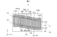
- FIG. 1 is a plan view showing one configuration example of an acoustic wave device according to Embodiment 1.
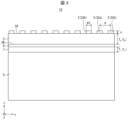
- FIG. FIG. 2 is a diagram schematically showing the laminated structure of the acoustic wave device according to Embodiment 1; It is a figure which shows another structural example of an elastic wave element.
- FIG. 4 is a contour diagram showing the relationship between tp and ti and MaxPhase obtained as a result of simulation, and showing regions REG1A and REG1B.
- FIG. 4 is a contour diagram showing the relationship between tp and ti and MaxPhase obtained as a result of simulation, and showing regions REG2A and REG2B.
- FIG. 10 is a diagram showing a configuration example of an acoustic wave filter according to Embodiment 2;
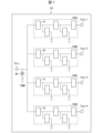
- FIG. 11 is a diagram showing a configuration example of a branching filter according to Embodiment 3;
- FIG. 5 is a diagram showing an example of frequency characteristics of first to fourth acoustic wave elements as oblique resonators;
- FIG. 4 is a diagram showing an example of frequency characteristics of a normal resonator; It is a figure which shows an example of the frequency characteristic of an oblique resonator.
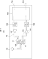
- FIG. 12 is a diagram illustrating a schematic configuration of a communication device according to Embodiment 4;
- Embodiment 1 The elastic wave device 1 of Embodiment 1 will be described below.
- members having the same functions as the members explained in the first embodiment are denoted by the same reference numerals in the subsequent embodiments, and the explanation thereof will not be repeated.
- descriptions of well-known technical matters are also omitted as appropriate.
- Each configuration and each numerical value described in this specification are merely examples unless otherwise specified. Therefore, unless otherwise specified, the positional relationship of each member is not limited to the examples in each figure. Also, each member is not necessarily illustrated to scale.
- FIG. 1 is a plan view showing a configuration example of an acoustic wave device 1.
- FIG. FIG. 1 shows a SAW (Surface Acoustic Wave) element as an example of an acoustic wave element.
- the orthogonal coordinate system (xyz coordinate system) shown in FIG. 1 is introduced for convenience.
- the x direction in the example of Embodiment 1 is the propagation direction of the elastic wave propagating through the piezoelectric film 2 of the elastic wave element 1 .
- the y-direction is an example of a direction crossing the x-direction in the plan view.
- FIG. 2 is a diagram schematically showing the laminated structure of the acoustic wave device 1.
- the z-direction in the example of Embodiment 1 is the thickness direction of each member of the acoustic wave device 1 .
- the term upper surface is used with the positive direction of the z-direction being the upper side.
- the term lower surface is used, with the negative direction of the z-direction defined as downward.
- the elastic wave according to one aspect of the present disclosure is not limited to SAW.
- the elastic wave may be a wave whose propagation direction can be considered.
- the elastic wave may be BAW (Bulk Acoustic Wave), for example. Therefore, another example of the acoustic wave device according to one aspect of the present disclosure is a BAW device. Therefore, the elastic wave filter according to one aspect of the present disclosure may be a SAW filter or a BAW filter.
- the acoustic wave element 1 includes (i) a piezoelectric film 2, (ii) an IDT (Interdigital Transducer) electrode 3 located on the upper surface 2A of the piezoelectric film 2, (iii) a low-frequency sound velocity film 7, and (iv) a support substrate. 5 and .
- the IDT electrodes are also called excitation electrodes.
- the IDT electrode 3 is located between two ports (terminals) P1 and P2. Ports P1 and P2 may be input and output ports, respectively.
- the acoustic wave device 1 may have a pair of reflectors 4A and 4B corresponding to the IDT electrodes 3.
- Each of reflectors 4A and 4B is also generically referred to as reflector 4 in this specification.
- the reflectors 4 may be positioned so as to sandwich the IDT electrodes 3 in the x-direction.
- the piezoelectric film 2 may be made of a single crystal material having piezoelectric properties.
- the material of the piezoelectric film 2 may be lithium tantalate (also called LiTaO 3 :LT) or lithium niobate (also called LiNbO 3 :LN).
- the piezoelectric film 2 may be an LT film.
- the support substrate 5 supports each part of the acoustic wave device 1 . Therefore, as shown in FIG. 2, the support substrate 5 may be positioned on the lower surface 2B side of the piezoelectric film 2 .
- the support substrate 5 may be configured such that the acoustic velocity of the elastic wave propagating through the support substrate 5 is higher than the acoustic velocity of the elastic wave propagating through the piezoelectric film 2 .
- Examples of materials for the support substrate 5 include Si, sapphire, crystal, and AlN.
- the support substrate 5 may be a Si substrate.
- the low sound velocity film 7 may be interposed between the piezoelectric film 2 and the support substrate 5 . As shown in FIG. 2 , the sound velocity film 7 may be positioned below the piezoelectric film 2 and above the support substrate 5 . The piezoelectric film 2 and the support substrate 5 may be bonded via the low-temperature film 7 . The low acoustic velocity film 7 may be configured such that the acoustic velocity of the acoustic wave propagating through the low acoustic velocity membrane 7 is lower than the acoustic velocity of the acoustic wave propagating through the piezoelectric membrane 2 . Silicon oxide (SiO x ) can be given as an example of the material of the low sound velocity film 7 . As an example, the low sound velocity film 7 may be a SiO2 film.
- sound velocity in this specification means the sound velocity of a bulk wave that is slower than the sound velocity of a bulk wave propagating through the piezoelectric film 2.
- high sonic speed means a bulk wave that is faster than the bulk wave propagating through the piezoelectric film 2 .
- Bulk wave speeds of sound may be compared relative to any one of longitudinal, fast shear, and slow shear waves.
- the thickness of the IDT electrode 3 is represented by s, the electrode finger pitch of the IDT electrode 3 by p, the thickness of the piezoelectric film 2 by Tp, and the thickness of the low-frequency film 7 by Ti.
- p is, for example, the pitch (repetition interval) in the x direction between the centers of a plurality of electrode fingers 32 (described later) of the IDT electrode 3 .
- the IDT electrode 3 may have a first comb-teeth electrode 30a (comb-teeth electrode on the port P1 side) and a second comb-teeth electrode 30b (comb-teeth electrode on the port P2 side).
- the first comb-teeth electrode 30 a and the second comb-teeth electrode 30 b are also collectively referred to as the comb-teeth electrode 30 .
- each member corresponding to the first comb-teeth electrode is appropriately suffixed with a
- each member corresponding to the second comb-teeth electrode is appropriately suffixed with b.
- Generic names corresponding to the comb-teeth electrodes 30 are used appropriately for these members as well.
- the comb-teeth electrode 30 may have two busbars 31 (a first busbar 31a and a second busbar 31b) facing each other in the y direction.
- Bus bar 31 may be formed in an elongated shape that has a substantially constant width and extends linearly. However, the width of the busbar 31 may not necessarily be constant.
- the comb-teeth electrode 30 includes a plurality of electrode fingers 32 extending in the y direction from one busbar 31 (eg, first busbar 31a) to the other busbar 31 (eg, second busbar 31b).
- the first electrode fingers 32a and the second electrode fingers 32b may be alternately and repeatedly positioned on the upper surface 2A of the piezoelectric film 2 so as to have substantially constant intervals in the x direction.
- the first electrode finger 32a may be connected to the first bus bar 31a.
- the second electrode finger 32b is connected to the second bus bar 31b and may be interposed with each of the plurality of first electrode fingers 32a.
- the comb-teeth electrode 30 extends from one busbar 31 (eg, first busbar 31a) to the other busbar 31 (eg, second busbar 31b) in the y-direction, and the other busbar 31 (eg, second busbar 31b) It may have a plurality of dummy electrode fingers 35 facing the tips of the electrode fingers 32 extending from the bus bar 31 .
- the pitch of the dummy electrode fingers 35 may be set equal to the pitch of the electrode fingers 32 . Therefore, the first dummy electrode fingers 35a may be connected to the first bus bar 31a and face the tips of the plurality of second electrode fingers 32b.
- the second dummy electrode fingers 35b are connected to the second bus bar 31b and may face the tips of the plurality of first electrode fingers 32a.
- the direction connecting the tips of the plurality of first electrode fingers 32a may be inclined with respect to the x direction.
- the virtual line L1 connecting the tips of the plurality of first electrode fingers 32a may be inclined with respect to the x direction.
- the virtual line L1 may form an inclination angle A1 (first inclination angle) with respect to the x-axis.
- the direction connecting the tips of the plurality of second electrode fingers 32b may be inclined with respect to the x direction.
- the virtual line L2 connecting the tips of the plurality of second electrode fingers 32b may be inclined with respect to the x direction.
- the virtual line L2 may form an inclination angle B1 (second inclination angle) with respect to the x-axis.
- the first tilt angle and the second tilt angle may be set to be equal to each other, or may be set to be different from each other.
- FIG. 1 illustrates a case where the first tilt angle and the second tilt angle are equal.
- the absolute values of each of the first tilt angle and the second tilt angle may be, for example, greater than 2° and less than or equal to 10°.
- the elastic wave device 1 having a non-zero first tilt angle and a non-zero second tilt angle is referred to as an oblique acoustic wave device (oblique resonator).
- oblique acoustic wave element According to the oblique acoustic wave element, lateral mode spurious (lateral mode ripple) in the acoustic wave element can be reduced (see Patent Document 1).
- the elastic wave element 1 is not limited to an oblique elastic wave element.
- the acoustic wave device 1 may be a normal acoustic wave device.
- the normal acoustic wave device means the acoustic wave device 1 in which both the first tilt angle and the second tilt angle are zero.
- a normal acoustic wave device may also be referred to as a normal resonator.
- the area where the first electrode finger 32a and the second electrode finger 32b intersect is referred to as an intersecting area.
- the shape of the intersection area may be defined by (i) virtual lines L1 and L2 and (ii) the electrode fingers 32 located on the reflector 4 side.
- the shape of the intersection region in the example of FIG. 1 is a parallelogram. Accordingly, FIG. 1 illustrates the IDT electrode 3 having a parallelogram-shaped outer shape.
- the length of the electrode fingers 32 in the x direction is referred to as the width of the electrode fingers 32.
- the width w1 (see FIG. 2) of each electrode finger 32 may be appropriately set according to, for example, electrical characteristics required of the acoustic wave device 1. As shown in FIG. As an example, w1 may be set according to p (electrode finger pitch). In this specification, the ratio of the width of the electrode finger to the pitch of the electrode finger, that is, w1/p is referred to as the duty of the electrode finger. w1 may be approximately constant. However, w1 does not necessarily have to be constant in one electrode finger 32 over the entire y direction. In the following description, w1 indicates, for example, the width of the electrode fingers 32 in the central portion of the intersecting region.
- the width w2 of the second dummy electrode fingers 35b may be set larger than the width w1 of the electrode fingers 32 in at least part of the intersection region.
- the width w3 of the first dummy electrode fingers 35a may also be set larger than the width w1 of the electrode fingers 32 in at least part of the intersection region.
- w2 and w3 are set equal to each other.
- w2 and w3 may be set larger than the width w1 of the electrode fingers 32 (eg, the width of the first electrode finger and the width of the second electrode finger) in at least part of the intersection region. According to this configuration, transverse mode spurious in the acoustic wave device 1 can be further reduced. As an example, w2 and w3 may be set larger than the average value of the widths w1 of the plurality of electrode fingers 32 in the intersecting regions.
- the area closer to the first bus bar 31a than the imaginary line L3 connecting the tips of the plurality of first dummy electrode fingers 35a is referred to as the first dummy area.
- a region closer to the second bus bar 31b than the imaginary line L4 connecting the tips of the plurality of second dummy electrode fingers 35b is referred to as a second dummy region.
- the width of the first electrode finger 32a located on the first dummy electrode finger side may be set larger than w1.
- the width of the second electrode finger 32b located on the side of the second dummy electrode finger may also be set larger than w1.
- the width of the electrode finger 32 is set to a value equal to w2.
- the root portion of the electrode finger 32 may be formed wider than the other portions of the electrode finger. According to this configuration, transverse mode ripples in the acoustic wave device 1 can be effectively reduced (see Patent Document 1).
- the duty of the first dummy electrode finger 35a (referred to as Dutyd1 for convenience) and the duty of the second dummy electrode finger 35b (referred to as Dutyd2 for convenience) are: It may be set larger than the Duty of the first electrode fingers 32a (referred to as Duty1 for convenience) and the Duty of the second electrode fingers 32b (referred to as Duty2 for convenience) in the central portion of the intersecting region. According to this configuration, transverse mode spurious in the acoustic wave device 1 can be further reduced.
- Dutyd1 and Dutyd2 may be set larger than Duty1 and Duty2 in the entire intersection area. According to this configuration, the transverse mode ripple in the acoustic wave device 1 can be further reduced.
- s when the elastic wave element 1 is an oblique elastic wave element, s may be 0.065 ⁇ or less (that is, 0.13p or less). According to this configuration, it is possible to improve the loss characteristics of the acoustic wave filter including the acoustic wave element 1 .
- FIG. 3 is a diagram showing another configuration example of the acoustic wave device 1 (referred to as an acoustic wave device 1V for convenience).
- FIG. 3 is a diagram paired with FIG.
- the acoustic wave device 1V may have a high acoustic velocity film 9 .
- the high acoustic velocity film 9 may be configured such that the acoustic velocity of the elastic wave propagating through the high acoustic velocity membrane 9 is higher than the acoustic velocity of the elastic wave propagating through the piezoelectric membrane 2 .
- the material of the high acoustic velocity film 9 include Al 2 O 3 and the like. Therefore, the high acoustic velocity film 9 may be an Al 2 O 3 film.
- the high acoustic velocity film 9 may be interposed between the piezoelectric film 2 and the low acoustic velocity film 7 . That is, the high acoustic velocity film 9 may be positioned below the piezoelectric film 2 and above the low acoustic velocity film 7 .
- the position of the high acoustic velocity film 9 is not limited to the example shown in FIG.
- the high acoustic velocity film 9 may be interposed between the low acoustic velocity film 7 and the support substrate 5 . That is, the high acoustic velocity film 9 may be positioned below the low acoustic velocity film 7 and above the support substrate 5 .
- the inventors of the present application performed simulations by FEM (Finite Element Method) and evaluated the characteristics of the acoustic wave device according to one aspect of the present disclosure. Specifically, the inventors performed the simulation and examined the relationship between tp and ti and the maximum phase value (MaxPhase) of the impedance of the acoustic wave device.
- the phase of impedance is simply referred to as phase.
- FIG. 4 and 5 are contour diagrams showing the relationship between tp and ti and MaxPhase obtained as a result of simulation. 4 and 5, the horizontal and vertical axes represent tp and ti (unit: ⁇ ), respectively. Also, the height axis indicates MaxPhase (unit: degree).
- FIG. 4 shows regions REG1A and REG1B, which will be described below.
- FIG. 5 shows regions REG2A and REG2B, which will be described below. The point Px shown in FIG. 5 will be described in a third embodiment below.
- the inventors set the piezoelectric film 2 as an LT film and the low-temperature film 7 as an SiO 2 film.
- the inventors varied tp and ti by varying Tp and Ti.
- the inventors derived MaxPhase corresponding to each pair of tp and ti by simulation.
- MaxPhase is one of the indicators of the performance of acoustic wave devices.
- the ideal maximum value of MaxPhase is 90°. It is known that the higher the MaxPhase (that is, the closer the MaxPhase is to 90°), the smaller the resonance loss in the acoustic wave device.
- tp and ti may be located within region REG1A shown in FIG.
- the region REG1A is a region in the tp-ti plane that satisfies the condition MaxPhase ⁇ 89.2° in the simulation result.
- tp and ti may satisfy the above formula (1).
- tp and ti may be located within region REG1B shown in FIG. Equation (1) is an ellipse representing region REG1B in the tp-ti plane. Most of region REG1B is located within region REG1A. Therefore, the loss characteristics of the acoustic wave device can be improved also by selecting tp and ti that satisfy equation (1).
- tp and ti may be located within region REG2A shown in FIG.
- the region REG2A is a region in the tp-ti plane that satisfies the condition MaxPhase ⁇ 89.3° in the simulation result.
- the region REG2A is a partial region of the region REG1A.
- tp and ti are represented by formula (4) below, ...(4) may be satisfied.
- tp and ti may be located within region REG2B shown in FIG. Equation (4) is an ellipse representing the region REG2B in the tp-ti plane.
- the region REG2B is a partial region of the region REG1B.
- Most of region REG2B is located within region REG2A. Therefore, by selecting tp and ti that satisfy equation (4), the loss characteristics of the acoustic wave device can be further improved.
- FIG. 6 is a diagram showing a configuration example of the elastic wave filter 100 according to the second embodiment.
- the elastic wave filter 100 may be configured as a ladder-type filter in which a plurality of elastic wave elements 1 are arranged in a ladder shape.
- the elastic wave filter 100 in the example of FIG. 6 has a plurality of (eg, three) series resonators 1S and a plurality of (eg, two) parallel resonators 1P as the plurality of acoustic wave elements 1. good.
- a plurality of (eg, three) series resonators 1S and a plurality of (eg, two) parallel resonators 1P as the plurality of acoustic wave elements 1. good.
- each of the three series resonators 1S when distinguished, they are denoted as series resonators 1S-1 to 1S-3.
- parallel resonators 1P-1 to 1P-2 are denoted as parallel resonators 1P-1 to 1P-2, respectively.
- the elastic wave filter 100 may be connected to the input terminal Tin and the output terminal Tout.
- the input terminal Tin is simply abbreviated as Tin as appropriate.
- the acoustic wave filter 100 may be configured as a frequency filter that filters an electrical signal input to Tin and outputs the filtered electrical signal to Tout.
- the acoustic wave filter 100 may have a series wiring SL connecting the plurality of series resonators 1S and a plurality of parallel wirings PL connecting the plurality of parallel resonators 1P. Acoustic wave filter 100 may be connected to a plurality of ground terminals TGND corresponding to each of a plurality of PLs. In the example of FIG. 6, the acoustic wave filter 100 has two PLs. Therefore, acoustic wave filter 100 is connected to two TGNDs. When distinguishing between the two PLs, they are denoted as PL-1 to PL-2. Also, when distinguishing between the two TGNDs, they are denoted as TGND-1 to TGND-2.
- series resonators 1S-1 to 1S-3 may be connected to Tin and Tout through SL, respectively.
- series resonator 1S-1 is the closest series resonator to Tin.
- the series resonator 1S-3 is the closest to Tout (in other words, the farthest from Tin).
- the parallel resonator 1P-1 is the parallel resonator closest to Tin.
- the parallel resonator 1P-2 is the parallel resonator closest to Tout.
- PL-1 branches from SL between series resonators 1S-1 and 1S-2 and is connected to TGND-1.
- PL-2 branches from SL between series resonators 1S-2 and 1S-3 and is connected to TGND-2.
- parallel resonators 1P-1 to 1P-2 may be connected to TGND-1 to TGND-2 via PL-1 to PL-2, respectively.
- the electrical signal can be filtered by releasing unnecessary components contained in the electrical signal to TGND via the parallel resonator 1P.
- the elastic wave filter 100 may be a frequency filter having a plurality of elastic wave elements 1 . Accordingly, as will be apparent to those skilled in the art, acoustic wave filter 100 may be configured as a multimode filter.
- FIG. 7 is a diagram showing a configuration example of the branching filter 101 according to the third embodiment.
- a duplexer is also called a multiplexer.
- the demultiplexer 101 may have a plurality of acoustic wave filters 100.
- FIG. In the example of FIG. 7, the demultiplexer 101 has four acoustic wave filters 100 (eg ladder filters).
- a duplexer 101 in FIG. 7 is an example of a quadplexer.
- the four elastic wave filters 100 are respectively called first filter 100A, second filter 100B, third filter 100C, and fourth filter 100D.
- the first filter 100A to fourth filter 100D may be connected to a common input terminal TCin.
- TCin may be an antenna terminal (see also Embodiment 4 below).
- TCin may be connected to TGND via reactor 99 .
- Each of the first filter 100A to fourth filter 100D may be connected to an individual output terminal.
- the first filter 100A to fourth filter 100D may be connected to output terminals Tout-1 to Tout-4, respectively.
- the first filter 100A to fourth filter 100D may be located on the same chip.
- the plurality of acoustic wave elements 1 can have a common support substrate 5 between the first filter 100A to the fourth filter 100D. Therefore, the thickness of the support substrate 5 can be common among the plurality of acoustic wave devices 1 .
- the plurality of acoustic wave elements 1 may have a common piezoelectric film 2 and sound velocity film 7 . Therefore, Tp and Ti can be common to the plurality of acoustic wave devices 1 .
- the plurality of acoustic wave elements 1 can be formed by, for example, a common film formation process. Therefore, s can be common to the plurality of acoustic wave devices 1 .
- the case where the first filter 100A to the fourth filter 100D are located on the same chip that is, the case where each thickness described above is common will be exemplified.
- the first filter 100A to the fourth filter 100D may each have different frequency characteristics.
- the passband of the first filter 100A may be located on the lower frequency side than the passband of the second filter 100B (see also FIG. 8 described below).
- the passband of the first filter 100A may be positioned on the lowest frequency side among all the passbands of the multiple (eg, four) elastic wave filters in the demultiplexer 101.
- the passband of the first filter 100A may be Band66Tx.
- the passband of the second filter 100B may be Band25Tx
- the passband of the third filter 100C may be Band25Rx
- the passband of the fourth filter 100D may be Band66Tx.
- the inventors have studied the frequency characteristics of each acoustic wave element in the branching filter 101 .
- one elastic wave element included in the first filter 100A, the second filter 100B, the third filter 100C, and the fourth filter 100D will be referred to as the first elastic wave element 1A, the second elastic wave element 1B, They are called a third elastic wave element 1C and a fourth elastic wave element 1D, respectively.
- FIG. 8 shows an example of frequency characteristics of the first elastic wave element 1A to the fourth elastic wave element 1D.
- All of the first elastic wave element 1A to the fourth elastic wave element 1D in the example of FIG. 8 are oblique resonators (oblique elastic wave elements).
- the first elastic wave element 1A corresponds to Band66Tx
- the second elastic wave element 1B corresponds to Band25Tx
- the third elastic wave element 1C corresponds to Band25Rx
- the fourth elastic wave element 1D corresponds to Band66Tx.
- FIG. 8 shows the frequency characteristics for different s (the thickness of the IDT electrode).
- each graph in FIG. 8 indicates frequency (unit: MHz).
- the graph denoted by reference numeral 8000A shows measured values of the impedance characteristics of the first elastic wave element 1A to the fourth elastic wave element 1D.
- the vertical axis in the graph indicates the absolute value (magnitude) of impedance (unit: ⁇ ).
- the graph 8000B in the example of FIG. 8 shows the measured values of the phase characteristics of the first elastic wave element 1A to the fourth elastic wave element 1D.
- the vertical axis in the graph indicates the phase (unit: degree).
- the graph 8000C shows phase characteristics of the first elastic wave element 1A to the fourth elastic wave element 1D derived by the simulation described in the first embodiment.
- the area around 90° on the vertical axis is shown enlarged.
- the point Px is positioned within the regions REG2A and REG2B and also within the regions REG1A and REG1B.
- MaxPhase increases as s decreases.
- resonance loss decreases as s decreases. Therefore, as an example, s may be set to 0.065 ⁇ or less in the first elastic wave element 1A to the fourth elastic wave element 1D. According to this configuration, it is possible to realize an oblique resonator with less resonance loss. As a result, it is possible to improve the loss characteristics of the acoustic wave filter including the oblique resonator.
- the passband of the first filter 100A may be located on the lower frequency side than the passband of the second filter 100B. According to this configuration, the resonance loss of the first elastic wave element 1A can be made smaller than the resonance loss of the second elastic wave element 1B. As a result, the loss characteristic of the first filter 100A can be further improved.
- the passband of the first filter 100A may be located on the lowest frequency side among the passbands of all the elastic wave filters in the demultiplexer 101. According to this configuration, the resonance loss of the first elastic wave element 1 ⁇ /b>A is the smallest among all the resonance losses of the oblique elastic waves in the branching filter 101 . As a result, the loss characteristics of the first filter 100A can be further improved.
- the inventors examined the frequency characteristics of the normal resonator and the oblique resonator. Specifically, the inventors studied the frequency characteristics of one acoustic wave element (eg, third acoustic wave element 1C) included in one frequency filter (eg, third filter 100C) in branching filter 101. did
- FIG. 9 shows an example of frequency characteristics of the normal resonator 1CN.
- the graph denoted by reference numeral 9000A shows measured values of the impedance characteristics of the normal resonator 1CN.
- a graph denoted by reference numeral 9000B shows measured values of the phase characteristics of the normal resonator 1CN.
- a graph denoted by reference numeral 9000C shows phase characteristics of the normal resonator 1CN derived by the simulation described in the first embodiment.
- the inventors examined the frequency characteristics of the third acoustic wave element 1C (for convenience, called the oblique resonator 1CS) as an oblique resonator.
- the inventors set the first tilt angle (A1) and the second tilt angle (B1) to ⁇ 6° in the oblique resonator 1CS.
- the inventors determined that w2 (the width of the second dummy electrode finger 35b) and w3 (the width of the first dummy electrode finger 35a) are the width w1 was set to a common value greater than the average value of
- FIG. 10 shows an example of frequency characteristics of the oblique resonator 1CS.
- FIG. 10 is a diagram paired with FIG. In FIG. 10, the graph denoted by reference numeral 10000A shows the measured values of the impedance characteristics of the oblique resonator 1CS. A graph denoted by reference numeral 10000B shows measured values of the phase characteristics of the oblique resonator 1CS. A graph denoted by reference numeral 10000C shows phase characteristics of the oblique resonator 1CS derived by the simulation described in the first embodiment.
- s may be set to 0.065 ⁇ or less. As shown in FIG. 10, according to this configuration, it is possible to achieve both loss improvement and spurious reduction in the acoustic wave device.
- FIG. 11 is a diagram illustrating a schematic configuration of the communication device 151 according to the fourth embodiment.
- the communication device 151 is an application example of an elastic wave filter according to an aspect of the present disclosure, and performs wireless communication using radio waves.
- the communication device 151 may include an acoustic wave filter according to one aspect of the present disclosure.
- the communication device 151 may include the demultiplexer 101 configured by the elastic wave filter.
- the communication device 151 in the example of FIG. 11 may include one branching filter 101 as the transmission filter 109 and another branching filter 101 as the reception filter 111 .
- a transmission information signal TIS including information to be transmitted is modulated and frequency-increased (converted into a high-frequency signal having a carrier frequency) by an RF-IC (Radio Frequency-Integrated Circuit) 153, and the transmission signal may be converted to TS.
- the bandpass filter 155 may remove unnecessary components other than the passband for transmission from the TS.
- the TS from which unnecessary components have been removed may be amplified by amplifier 157 and input to transmission filter 109 .
- the transmission filter 109 may remove unnecessary components outside the transmission passband from the input transmission signal TS.
- the transmission filter 109 may output the TS from which unnecessary components have been removed to the antenna 159 via an antenna terminal (eg, TCin described above).
- the antenna 159 may convert the TS, which is an electric signal input to itself, into radio waves as radio signals, and transmit the radio waves to the outside of the communication device 151 .
- the antenna 159 may convert a received radio wave from the outside into a reception signal RS, which is an electric signal, and input the RS to the reception filter 111 via the antenna terminal.
- the reception filter 111 may remove unnecessary components outside the reception passband from the input RS.
- the receive filter 111 may output to the amplifier 161 the receive signal RS from which the unnecessary components have been removed.
- the output RS may be amplified by amplifier 161 .
- the bandpass filter 163 may remove unnecessary components other than the reception passband from the amplified RS.
- the RF-IC 153 may frequency-reduce and demodulate the RS from which unnecessary components have been removed, and convert it into a received information signal RIS.
- the TIS and RIS may be low frequency signals (baseband signals) containing appropriate information.
- the TIS and RIS may be analog audio signals or digitized audio signals.
- the pass band of the radio signal may be set appropriately and may conform to various known standards.
Landscapes
- Physics & Mathematics (AREA)
- Acoustics & Sound (AREA)
- Surface Acoustic Wave Elements And Circuit Networks Thereof (AREA)
Priority Applications (1)
| Application Number | Priority Date | Filing Date | Title |
|---|---|---|---|
| JP2024504622A JPWO2023167034A1 (https=) | 2022-03-03 | 2023-02-20 |
Applications Claiming Priority (2)
| Application Number | Priority Date | Filing Date | Title |
|---|---|---|---|
| JP2022032852 | 2022-03-03 | ||
| JP2022-032852 | 2022-03-03 |
Publications (1)
| Publication Number | Publication Date |
|---|---|
| WO2023167034A1 true WO2023167034A1 (ja) | 2023-09-07 |
Family
ID=87883496
Family Applications (1)
| Application Number | Title | Priority Date | Filing Date |
|---|---|---|---|
| PCT/JP2023/005970 Ceased WO2023167034A1 (ja) | 2022-03-03 | 2023-02-20 | 弾性波素子、弾性波フィルタ、分波器、および通信装置 |
Country Status (2)
| Country | Link |
|---|---|
| JP (1) | JPWO2023167034A1 (https=) |
| WO (1) | WO2023167034A1 (https=) |
Citations (4)
| Publication number | Priority date | Publication date | Assignee | Title |
|---|---|---|---|---|
| WO2016208446A1 (ja) * | 2015-06-24 | 2016-12-29 | 株式会社村田製作所 | フィルタ装置 |
| JP2020102662A (ja) * | 2018-12-19 | 2020-07-02 | 京セラ株式会社 | 弾性波素子 |
| WO2020204036A1 (ja) * | 2019-04-04 | 2020-10-08 | 株式会社村田製作所 | 弾性波装置 |
| JP2021100280A (ja) * | 2018-11-14 | 2021-07-01 | 京セラ株式会社 | 弾性波装置、分波器および通信装置 |
-
2023
- 2023-02-20 JP JP2024504622A patent/JPWO2023167034A1/ja active Pending
- 2023-02-20 WO PCT/JP2023/005970 patent/WO2023167034A1/ja not_active Ceased
Patent Citations (4)
| Publication number | Priority date | Publication date | Assignee | Title |
|---|---|---|---|---|
| WO2016208446A1 (ja) * | 2015-06-24 | 2016-12-29 | 株式会社村田製作所 | フィルタ装置 |
| JP2021100280A (ja) * | 2018-11-14 | 2021-07-01 | 京セラ株式会社 | 弾性波装置、分波器および通信装置 |
| JP2020102662A (ja) * | 2018-12-19 | 2020-07-02 | 京セラ株式会社 | 弾性波素子 |
| WO2020204036A1 (ja) * | 2019-04-04 | 2020-10-08 | 株式会社村田製作所 | 弾性波装置 |
Also Published As
| Publication number | Publication date |
|---|---|
| JPWO2023167034A1 (https=) | 2023-09-07 |
Similar Documents
| Publication | Publication Date | Title |
|---|---|---|
| JP7169083B2 (ja) | 弾性波デバイスおよびマルチプレクサ | |
| US12324355B2 (en) | Acoustic wave device | |
| CN107210730B (zh) | 滤波器、分波器以及通信装置 | |
| CN102405596B (zh) | 天线共用器 | |
| CN107636961A (zh) | 弹性波滤波器装置 | |
| KR20180009354A (ko) | 멀티플렉서, 고주파 프론트 엔드 회로 및 통신 장치 | |
| CN107615661A (zh) | 弹性波装置以及通信装置 | |
| CN110892640A (zh) | 多工器、高频前端电路以及通信装置 | |
| CN111512548A (zh) | 弹性波滤波器、多工器、高频前端电路以及通信装置 | |
| CN111527699A (zh) | 弹性波滤波器 | |
| WO2017115870A1 (ja) | 弾性波フィルタ装置およびデュプレクサ | |
| JP6935220B2 (ja) | 弾性波素子、フィルタおよびマルチプレクサ | |
| CN110809858B (zh) | 多工器 | |
| CN111466083B (zh) | 弹性波滤波器、分波器以及通信装置 | |
| JP7117880B2 (ja) | 弾性波フィルタ、分波器および通信装置 | |
| CN211830723U (zh) | 弹性波滤波器装置以及复合滤波器装置 | |
| JP2021150893A (ja) | フィルタ、分波器及び通信装置 | |
| WO2018117060A1 (ja) | 弾性波共振器、フィルタ装置およびマルチプレクサ | |
| WO2023167034A1 (ja) | 弾性波素子、弾性波フィルタ、分波器、および通信装置 | |
| JP2025038204A (ja) | 弾性波装置、フィルタ、分波器及び通信装置 | |
| CN114080753A (zh) | 弹性波滤波器、分波器以及通信装置 | |
| JP7714113B2 (ja) | 弾性波素子、モジュール及び通信装置 | |
| CN113519121A (zh) | 弹性波滤波器装置以及多工器 | |
| JP7692109B2 (ja) | 弾性波フィルタ、分波器、および通信装置 | |
| JP2008283425A (ja) | 縦結合多重モード共振子型弾性表面波フィルタ |
Legal Events
| Date | Code | Title | Description |
|---|---|---|---|
| 121 | Ep: the epo has been informed by wipo that ep was designated in this application |
Ref document number: 23763293 Country of ref document: EP Kind code of ref document: A1 |
|
| ENP | Entry into the national phase |
Ref document number: 2024504622 Country of ref document: JP Kind code of ref document: A |
|
| NENP | Non-entry into the national phase |
Ref country code: DE |
|
| 122 | Ep: pct application non-entry in european phase |
Ref document number: 23763293 Country of ref document: EP Kind code of ref document: A1 |