WO2023162736A1 - 発振回路、及びバッファ回路 - Google Patents
発振回路、及びバッファ回路 Download PDFInfo
- Publication number
- WO2023162736A1 WO2023162736A1 PCT/JP2023/004668 JP2023004668W WO2023162736A1 WO 2023162736 A1 WO2023162736 A1 WO 2023162736A1 JP 2023004668 W JP2023004668 W JP 2023004668W WO 2023162736 A1 WO2023162736 A1 WO 2023162736A1
- Authority
- WO
- WIPO (PCT)
- Prior art keywords
- node
- circuit
- inverter
- voltage
- mos transistor
- Prior art date
- Legal status (The legal status is an assumption and is not a legal conclusion. Google has not performed a legal analysis and makes no representation as to the accuracy of the status listed.)
- Ceased
Links
Images





Classifications
-
- H—ELECTRICITY
- H03—ELECTRONIC CIRCUITRY
- H03B—GENERATION OF OSCILLATIONS, DIRECTLY OR BY FREQUENCY-CHANGING, BY CIRCUITS EMPLOYING ACTIVE ELEMENTS WHICH OPERATE IN A NON-SWITCHING MANNER; GENERATION OF NOISE BY SUCH CIRCUITS
- H03B5/00—Generation of oscillations using amplifier with regenerative feedback from output to input
- H03B5/30—Generation of oscillations using amplifier with regenerative feedback from output to input with frequency-determining element being electromechanical resonator
- H03B5/32—Generation of oscillations using amplifier with regenerative feedback from output to input with frequency-determining element being electromechanical resonator being a piezoelectric resonator
- H03B5/36—Generation of oscillations using amplifier with regenerative feedback from output to input with frequency-determining element being electromechanical resonator being a piezoelectric resonator active element in amplifier being semiconductor device
- H03B5/364—Generation of oscillations using amplifier with regenerative feedback from output to input with frequency-determining element being electromechanical resonator being a piezoelectric resonator active element in amplifier being semiconductor device the amplifier comprising field effect transistors
-
- H—ELECTRICITY
- H03—ELECTRONIC CIRCUITRY
- H03B—GENERATION OF OSCILLATIONS, DIRECTLY OR BY FREQUENCY-CHANGING, BY CIRCUITS EMPLOYING ACTIVE ELEMENTS WHICH OPERATE IN A NON-SWITCHING MANNER; GENERATION OF NOISE BY SUCH CIRCUITS
- H03B5/00—Generation of oscillations using amplifier with regenerative feedback from output to input
- H03B5/02—Details
- H03B5/04—Modifications of generator to compensate for variations in physical values, e.g. power supply, load, temperature
-
- H—ELECTRICITY
- H03—ELECTRONIC CIRCUITRY
- H03B—GENERATION OF OSCILLATIONS, DIRECTLY OR BY FREQUENCY-CHANGING, BY CIRCUITS EMPLOYING ACTIVE ELEMENTS WHICH OPERATE IN A NON-SWITCHING MANNER; GENERATION OF NOISE BY SUCH CIRCUITS
- H03B5/00—Generation of oscillations using amplifier with regenerative feedback from output to input
- H03B5/20—Generation of oscillations using amplifier with regenerative feedback from output to input with frequency-determining element comprising resistance and either capacitance or inductance, e.g. phase-shift oscillator
- H03B5/24—Generation of oscillations using amplifier with regenerative feedback from output to input with frequency-determining element comprising resistance and either capacitance or inductance, e.g. phase-shift oscillator active element in amplifier being semiconductor device
-
- H—ELECTRICITY
- H03—ELECTRONIC CIRCUITRY
- H03B—GENERATION OF OSCILLATIONS, DIRECTLY OR BY FREQUENCY-CHANGING, BY CIRCUITS EMPLOYING ACTIVE ELEMENTS WHICH OPERATE IN A NON-SWITCHING MANNER; GENERATION OF NOISE BY SUCH CIRCUITS
- H03B5/00—Generation of oscillations using amplifier with regenerative feedback from output to input
- H03B5/30—Generation of oscillations using amplifier with regenerative feedback from output to input with frequency-determining element being electromechanical resonator
- H03B5/32—Generation of oscillations using amplifier with regenerative feedback from output to input with frequency-determining element being electromechanical resonator being a piezoelectric resonator
-
- H—ELECTRICITY
- H03—ELECTRONIC CIRCUITRY
- H03B—GENERATION OF OSCILLATIONS, DIRECTLY OR BY FREQUENCY-CHANGING, BY CIRCUITS EMPLOYING ACTIVE ELEMENTS WHICH OPERATE IN A NON-SWITCHING MANNER; GENERATION OF NOISE BY SUCH CIRCUITS
- H03B5/00—Generation of oscillations using amplifier with regenerative feedback from output to input
- H03B5/30—Generation of oscillations using amplifier with regenerative feedback from output to input with frequency-determining element being electromechanical resonator
- H03B5/32—Generation of oscillations using amplifier with regenerative feedback from output to input with frequency-determining element being electromechanical resonator being a piezoelectric resonator
- H03B5/36—Generation of oscillations using amplifier with regenerative feedback from output to input with frequency-determining element being electromechanical resonator being a piezoelectric resonator active element in amplifier being semiconductor device
-
- H—ELECTRICITY
- H03—ELECTRONIC CIRCUITRY
- H03F—AMPLIFIERS
- H03F1/00—Details of amplifiers with only discharge tubes, only semiconductor devices or only unspecified devices as amplifying elements
- H03F1/02—Modifications of amplifiers to raise the efficiency, e.g. gliding Class A stages, use of an auxiliary oscillation
-
- H—ELECTRICITY
- H03—ELECTRONIC CIRCUITRY
- H03B—GENERATION OF OSCILLATIONS, DIRECTLY OR BY FREQUENCY-CHANGING, BY CIRCUITS EMPLOYING ACTIVE ELEMENTS WHICH OPERATE IN A NON-SWITCHING MANNER; GENERATION OF NOISE BY SUCH CIRCUITS
- H03B2200/00—Indexing scheme relating to details of oscillators covered by H03B
- H03B2200/003—Circuit elements of oscillators
- H03B2200/0034—Circuit elements of oscillators including a buffer amplifier
Definitions
- the present disclosure relates to oscillator circuits and buffer circuits.
- Oscillation circuits that use oscillators such as crystals invert and amplify the minute voltage generated by the oscillator when it is activated by an amplifier circuit composed of an inverter or the like, and feed back the amplified voltage to the oscillator repeatedly. A steady oscillation state is reached. At the time of start-up and steady oscillation, the oscillation circuit is required to oscillate in a stable manner and to be driven with low power consumption. In order to satisfy this demand, a configuration has been proposed in which the drain current of a P-type MOS transistor that constitutes an inverter included in an amplifier circuit is controlled according to the amplitude voltage of the oscillation signal (Patent Document 1).
- a three-stage inverter provided in an amplifier circuit, two second-stage inverters are connected in parallel, and one of the inverters has a resistor connected between the ground VSS and an N-type MOS transistor.
- the inverter output is connected to the gate of the P-type MOS transistor of the third stage inverter, the other inverter is connected to a resistor between the power supply voltage VDD and the P-type MOS transistor, and the inverter output is connected to the N-type of the third stage inverter.
- Patent Document 2 A configuration has been proposed in which the through current of the third-stage inverter is suppressed by connecting it to the gate of the MOS transistor
- An object of the present invention is to provide an oscillator circuit or the like that can be driven by electric power.
- an oscillation circuit includes an oscillator and an amplifier circuit that amplifies a voltage of the oscillator, wherein the amplifier circuit receives a first input A first inverter that outputs a signal to a first node and a second node, and a second inverter that receives the signals of the first node and the second node and outputs an output signal to a third node. and an inverter of , the amplifier circuit further having a variable resistor connected between the first node and the second node and controlled by a control signal.
- the oscillation circuit by controlling the variable resistor provided in the inverter with a control signal at startup and during steady oscillation, stable oscillation operation from startup to steady oscillation and during steady operation It is possible to suppress the power consumption caused by the through current.
- variable resistance by setting the variable resistance by the on-resistance of the transistor, it is possible to suppress the area increase.
- the optimum delay time can be set for the node Np or the node Nn, and the oscillation circuit can be used for general purposes. It becomes possible.
- multistage means that it is three or more stages.
- the through current of the inverter is suppressed and the power supply voltage fluctuation at the time of logic transition is suppressed. and deterioration of EMI characteristics can be suppressed.
- the supply current to the vibrator is suppressed, and the margin of the excitation level can be expanded.
- the amplifier circuit when used as a buffer circuit, it is possible to reduce power consumption, improve power supply voltage fluctuations, and improve EMI characteristics.
- FIG. 1 is a circuit diagram showing the configuration of an oscillation circuit according to the first embodiment of the present disclosure.
- FIG. 2 is a circuit diagram showing the variable resistor of FIG. 1;
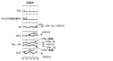
- FIG. 3A is a waveform diagram at startup of the oscillation circuit according to the first embodiment of the present disclosure.
- 3B is a waveform diagram during steady oscillation of the oscillation circuit according to the first embodiment of the present disclosure;
- FIG. 4 is a circuit diagram showing Modification 1 of the variable resistor in FIG.
- FIG. 5 is a circuit diagram showing Modification 2 of the variable resistor in FIG.
- FIG. 6 is a circuit diagram showing Modification 1 of the buffer circuit of FIG.
- FIG. 7 is a circuit diagram showing Modification 3 of the variable resistor in FIG.
- FIG. 1 is a circuit diagram showing the configuration of an oscillation circuit according to the first embodiment of the present disclosure.
- FIG. 2 is a circuit diagram showing the variable resistor of FIG. 1
- FIG. 3A is a waveform diagram at startup of the
- FIG. 8 is a circuit diagram showing a buffer circuit in Modification 3 of the variable resistor in FIG.
- FIG. 9 is a waveform diagram showing the operation of Modification 1 of the buffer circuit of FIG.
- FIG. 10 is a circuit diagram showing Modification 4 of the variable resistor in FIG.
- FIG. 1 is a circuit diagram showing the configuration of an oscillation circuit 100 of the present disclosure
- 101 is a vibrator
- C101 and C102 are load capacitances connected to both ends of the vibrator 101
- A1 amplifies the voltage generated by the vibrator 101.
- SIG is a control signal for controlling the amplifier circuit A1.
- the oscillation circuit 100 includes an oscillator 101 and an amplifier circuit A1.
- the amplifier circuit A1 has an input terminal IN, an output terminal OUT, and a control terminal PN for inputting a control signal SIG. and a feedback resistor R101 for feedback.
- the voltage VOUT is fed back to set VIN_dc, which is the DC voltage of the inverter INV101 (hereinafter, the DC voltage of the inverter input is referred to as DC bias).
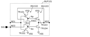
- the buffer circuit BUF101 has an input node ND1, an output node ND2, and a node ND3 to which the control signal SIG is applied via the control terminal PN.
- the buffer circuit BUF101 includes an inverter INV102 and an inverter INV103.
- the inverter INV102 is an example of a first inverter that outputs a first input signal to the node Np and the node Nn.
- Node Np is an example of a first node
- node Nn is an example of a second node.
- the inverter INV102 further includes a P-type MOS transistor TR101 and an N-type MOS transistor TR102 having the node ND1 as an input, and a variable resistor R102 connected between the nodes Np and Nn and controlled by a control signal.
- the variable resistor R102 is a variable resistor with a resistance value Rn provided between the P-type MOS transistor TR101 and the N-type MOS transistor TR102.
- the inverter INV103 is an example of a second inverter that receives signals from the nodes Np and Nn and outputs an output signal to the node ND2.
- Node ND2 is an example of a third node.
- Inverter INV103 connects P-type MOS transistor TR103 connected to node Np, which is the output node of P-type MOS transistor TR101, and N-type MOS transistor TR104, which is connected to node Nn which is the output node of N-type MOS transistor TR102. Prepare.
- FIG. 2 is a circuit diagram showing the variable resistor R102.
- R103 is a resistor having a resistance value Rc
- SW1 is a switch composed of a P-type MOS transistor TR105 and an N-type MOS transistor TR106
- INV104 is an inverter for outputting an inverted logic signal of the control signal SIG.
- the variable resistor R102 has a resistor R103 and a switch SW1.
- the resistor R103 is an example of a first resistor.
- the switch SW1 is an example of a switch that short-circuits the first resistor (that is, the resistor R103).
- the resistance value Rc of the resistor R103 and the resistance value Ron of the switch SW1 are designed so that the resistance value Rc>the resistance value Ron.
- the resistance value of the variable resistor R102 is switched by the control signal between when the oscillator circuit 100 starts up and when it oscillates normally. More specifically, the resistance value of the variable resistor R102 is switched by the control signal so as to be lower than that during steady oscillation of the oscillation circuit 100 when the oscillation circuit 100 is started.
- the resistance value Ron of the variable resistor R102 is changed to a high resistance value Rc (hereinafter referred to as high resistance Rc) and a low resistance value Ron (hereinafter referred to as low resistance Ron). described).
- the resistance value of the switch SW1 is determined by the ON resistance of the transistor.
- FIGS. 3A and 3B are waveform diagrams during start-up and steady oscillation of the oscillation circuit 100 according to Embodiment 1 of the present disclosure, respectively.
- the operation of the oscillation circuit 100 shown in FIGS. 1 and 2 will be described using the waveform diagrams of FIGS. 3A and 3B.
- ⁇ i is the amplitude of the voltage generated by the vibrator 101, i is counted each time the output voltage VOUT is fed back from the amplifier circuit A1 to the vibrator 101, and the initial value is 1, and then a natural number. To increase. Also, ⁇ t indicates the phase.
- the control signal SIG is set to "L”.
- the P-type MOS transistor TR105 and the N-type MOS transistor TR106 of the variable resistor R102 are turned on, and the resistance value Rn between the node Np and the node Nn is set to the low resistance Ron of the switch SW1.
- the DC bias VIN_dc of the inverter INV101 connected to the input terminal IN becomes approximately (VDD/2) by feedback of the voltage VOUT of the output terminal OUT via the feedback resistor R101.
- K1 is the voltage amplification factor of the inverter INV101
- .theta.1 is the delay component which is a positive value when the logic of the inverter INV101 is inverted.
- the voltage VND1 of the node ND1 is input to the P-type MOS transistor TR101 and the N-type MOS transistor TR102 of the inverter INV102.
- the ON resistance of the P-type MOS transistor TR101 is RPinv
- the ON resistance of the N-type MOS transistor TR102 is RNinv
- the DC voltage levels at the nodes Np and Nn are as follows.
- VNp_dc VDD ⁇ [(Ron+RNinv)/(RPinv+Ron+RNinv)]
- VNn_dc VDD ⁇ [(RNinv)/(RPinv+Ron+RNinv)] (4)
- K2 is the voltage amplification of the inverter INV102
- ⁇ 2 is the positive value delay component at the time of logical inversion of the inverter INV102
- Ron the resistance value of the variable resistor R102
- the gate-source voltage Vgs of the P-type MOS transistor TR103 and the N-type MOS transistor TR104 of the inverter INV103 with VNp or VNn as the input is set to It becomes possible to set the voltage to Vgs, and it becomes possible to drive the inverter INV103.
- Vgs can be set to be even larger. Therefore, it can be seen that the transistor can be turned on even with a minute voltage generated by the vibrator at the time of start-up.
- the voltage VNp and the voltage VNn of the node Np and the node Nn are applied to the P-type MOS transistor TR103 and the N-type MOS transistor TR104 of the inverter INV103, respectively.
- K3 is the voltage amplification factor of the inverter INV103
- .theta.3 is a positive value delay component at the time of logic inversion of the inverter INV103.
- the output voltage VOUT obtained by inverting and amplifying the voltage VIN of the input terminal IN by the amplifier circuit A1 is output to the output terminal OUT.
- the vibrator 101 When the output voltage VOUT is fed back to the vibrator 101, the vibrator 101 generates a minute voltage ⁇ 2 ⁇ sin( ⁇ t).
- sin( ⁇ t) ⁇ 0 ⁇ 2> ⁇ 1
- the vibrator When the output voltage VOUT is fed back to the vibrator 101, the vibrator generates a minute amplitude ⁇ 3 ⁇ sin( ⁇ t).
- the operation is the same as [time T1 to T2], and the oscillation operation is repeated while the voltage generated by the vibrator 101 is amplified.
- the output voltage VOUT of the output terminal OUT becomes an oscillation signal with an amplitude voltage VDD as shown in FIG. 3A.
- a steady oscillation state is established, and thereafter the amplitude voltage ⁇ n in the generated voltage of the vibrator 101 becomes constant.
- the oscillation operation can be performed by setting the resistance value Rn of the variable resistor R102 forming the inverter INV102 to the low resistance value Ron at the time of startup by the control signal SIG.
- the inverter INV102 may include a P-type MOS transistor TR101, an N-type MOS transistor TR102, and a variable resistor R102. Even if the inverter INV102 includes other devices, the resistance value Rpd between VDD and node Np and the resistance value Rnd between VSS and node Nn are given by equation (11). Ron ⁇ Rdp and Ron ⁇ Rdn (12) is satisfied.
- the voltages VNp and VNn of the nodes Np and Nn that satisfy the equation (12) and Ron that satisfies the equations (9) and (10) showing the relationship with each transistor of the inverter INV103 may be set. .
- the control signal SIG is "L"
- the resistance value Rn of the variable resistor R102 is set to the low resistance Ron of the switch SW1.
- the DC bias VIN_dc of the inverter INV101 connected to the input terminal IN becomes approximately (VDD/2) by feedback of the voltage VOUT of the output terminal OUT via the feedback resistor R101.
- the amplitude voltage ⁇ n ⁇ K1 of the voltage VND1 is ( ⁇ n ⁇ K1)>>(VDD ⁇ VSS).
- ⁇ n is a positive value delay component when the logic of the inverter INV101 is inverted.
- the output voltage VOUT is fed back to the oscillator 101, and the oscillator 101 generates ⁇ n ⁇ sin( ⁇ t).
- ⁇ t 180° to 360°.
- Inverters INV102 and INV103 perform the same operation as [time T1 to T2], and the output voltage VOUT obtained by inverting and amplifying the voltage VIN of the input terminal IN by the amplifier circuit A1 is output to the output terminal OUT.
- the oscillator 101 By feeding back the output voltage VOUT to the oscillator 101, the oscillator 101 generates a minute voltage ⁇ n ⁇ sin( ⁇ t). Here, 360° ⁇ t ⁇ 540°.
- the state becomes the same as that at time [T1], and the above operation is repeated.
- an oscillation signal of amplitude voltage VDD is steadily output from the output terminal OUT.
- the P-type MOS transistor TR101 When the P-type MOS transistor TR101 is turned on, the voltage VNp of the node Np first transitions from VSS to VDD, and the P-type MOS transistor TR103 of the inverter INV103 is turned off. On the other hand, the voltage VNn of the node Nn transitions from VSS to VDD through the variable resistor R102 set to the high resistance value Rc. As a result, the N-type MOS transistor TR104 of the inverter INV103 is turned on, and the voltage VOUT of the output terminal OUT transitions from VDD to VSS.
- the transition time of the voltage VNn of the node Nn is delayed by the time set by the time constant ⁇ r, it is possible to suppress the through current from the P-type MOS transistor TR103 to the N-type MOS transistor TR104 of the inverter INV103.
- the N-type MOS transistor TR102 By turning on the N-type MOS transistor TR102, the voltage VNn of the node Nn first transitions from VDD to VSS, and the N-type MOS transistor TR104 of the inverter INV103 is turned off. On the other hand, the voltage VNp of the node Np transitions from VDD to VSS via the variable resistor R102 set to the high resistance value Rc. As a result, the P-type MOS transistor TR103 of the inverter INV103 is turned on with a delay with respect to the transition time of the N-type MOS transistor TR104, and the voltage VOUT of the output terminal OUT transitions from VSS to VDD.
- the transition time of the voltage VNp of the node Np is delayed by the time set by the time constant ⁇ f, it is possible to suppress the through current from the P-type MOS transistor TR103 to the N-type MOS transistor TR104 of the inverter INV103.
- the time constant ⁇ f Rc ⁇ Cp (Cp is the gate capacitance of the P-type MOS transistor TR103 of the inverter INV103, etc.).
- the MOS transistor TR104 can be set to an off-off state, and wasteful current consumption due to through current can be suppressed.
- control signal SIG switches the resistance value Rn of the variable resistor R102 provided between the P-type MOS transistor TR101 and the N-type MOS transistor TR102 of the inverter INV102 to a low resistance Ron at startup and a high resistance Rc at steady oscillation. This enables stable oscillation operation from start-up to steady-state oscillation and low power consumption drive during steady-state operation.
- the timing of switching the resistance value Rn of the variable resistor R102 from the low resistance Ron to the high resistance Rc by the control signal SIG may be any timing as long as the oscillation circuit 100 reaches steady oscillation from the start-up.
- the switching may be performed after a certain period of time has elapsed, or may be switched at an arbitrary timing to drive the oscillation circuit 100 with low power consumption.
- the vibrator may be a piezoelectric vibrator such as crystal or ceramic.
- the amplifier circuit A1 only needs to include the buffer circuit BUF101, and the number of inverter stages and the configuration of the inverter INV101 are not limited to this as long as the amplifier circuit A1 is configured to invert and amplify.
- another element such as a DC cut capacitor or a damping resistor may be provided between the vibrator 101 and the input terminal IN or between the vibrator 101 and the output terminal OUT.
- the buffer circuit BUF101 is a potential difference generation circuit that generates a potential difference between the first node and the second node, and may include a potential difference generation circuit that switches the potential difference by a control signal.
- the differential voltage (VNp_dc ⁇ VNn_dc) between the DC biases VNp_dc and VNn_dc of the input voltages VNp and VNn of the 2-input inverter INV103 provided as an output stage is adjusted in two or more stages according to the control signal.
- Any configuration using a switchable potential difference generating circuit may be used.
- the potential difference generating circuit may include a variable resistor consisting of a resistor and a switch that shorts the resistor, and switch the switch in response to a control signal.
- the potential difference generating circuit may be configured by a diode or a diode-connected transistor and a switch as the variable resistor R102 of the inverter INV102.
- the potential difference generation circuit is composed of a resistance circuit including both or one of a resistor and a transistor, and the inverter INV102 is provided with a current adjustment circuit capable of setting a plurality of currents, and switches the current adjustment circuit according to the control signal. good too.
- the potential difference generation circuit includes a current source or a current adjustment circuit that can set a plurality of current values for the inverter INV102, and switches the current amount at the time of logic transition of the inverter INV102 according to the control signal, thereby switching the node Nn and the node Np. It may be configured to switch the potential difference generated in a resistance circuit composed of resistors, transistors, diodes, etc., provided between and, and is not limited to this as long as a similar function can be realized in this way. Also, the switch of the variable resistor R102 may be composed of a P-type MOS transistor or an N-type MOS transistor.
- FIG. 4 shows Modification 1 of the variable resistor R102 according to the first embodiment of the present disclosure, in which the switch SW1 in FIG. 2 is replaced with a series connection of a switch SW2a and a switch SW2b.
- the control signal SIG consists of a control signal SIGA and a control signal SIGB
- INV201 is an inverter for logically inverting the control signal SIGA
- INV202 is an inverter for logically inverting the control signal SIGB
- SW2a is a P-type MOS transistor TR201 and an N-type MOS transistor TR202.
- SW2b is a switch composed of a P-type MOS transistor TR203 and an N-type MOS transistor TR204
- R201 and R202 are resistors
- Nr is a node between the resistors R201 and R202.
- the resistance value Rn1 is set by switching between the resistance value Rc1 of the resistor R201 and the resistance value Ron1 of the switch SW2a by the control signal SIGA.
- a resistance value Ron1 is a combined resistance when both the P-type MOS transistor TR201 and the N-type MOS transistor TR202 are turned on, and is lower than the resistance value Rc1.
- the resistance value Rn2 is set by switching between the resistance value Rc2 of the resistor R202 and the resistance value Ron2 of the switch SW2b by the control signal SIGB.
- a resistance value Ron2 is a combined resistance when both the P-type MOS transistor TR203 and the N-type MOS transistor TR204 are turned on, and is lower than the resistance value Rc2.
- the resistance value Rn between the node Np and the node Nn can be switched in multiple steps to (Rc1+Rc2), (Rc1+Ron2), (Ron1+Rc2), and (Ron1+Ron2). It becomes possible. That is, the resistance value of the variable resistor R102 can be switched in multiple stages. This makes it possible to set the time constants ⁇ r and ⁇ f described in the first embodiment in multiple stages.
- FIG. 5 shows a second modification of the variable resistor R102 according to the first embodiment of the present disclosure, in which the switch SW1 in FIG. 2 is replaced with a switch SW3a and the resistor R103 is replaced with a switch SW3b.
- the control signal SIG consists of the control signal SIGA and the control signal SIGB
- INV301 is an inverter that logically inverts the control signal SIGA
- INV302 is an inverter that logically inverts the control signal SIGB
- SW3a is a P-type MOS transistor TR301 and an N-type MOS transistor TR302.
- SW3b is a switch composed of a P-type MOS transistor TR303 and an N-type MOS transistor TR304.
- the resistance value Ron2 of the switch SW3b is increased by setting the channel width/channel length (that is, gate width/gate length) of the P-type MOS transistor TR303 and the N-type MOS transistor TR304 to be small. is preferably set to a higher resistance than the resistance value Ron1 of the switch SW3a.
- the variable resistor R102 includes a plurality of transistors having different ratios of gate width to gate length, which are transistor size ratios.
- the time constants ⁇ r and ⁇ f can be switched in multiple stages, even when the oscillation frequency of the oscillation circuit 100 is different, the optimum delay time can be set for the node Np or the node Nn, and the through current of the inverter INV103 can be reduced. Therefore, it is possible to drive with low power consumption. Moreover, since the time constants ⁇ r and ⁇ f are set by the on-resistance of the transistors, it is possible to reduce the circuit area of the variable resistor R102.
- variable resistor R102 by configuring the variable resistor R102 by combining a plurality of transistors and controlling the resistance value with a control signal, stable oscillation at startup and low power consumption drive at steady oscillation are possible. Furthermore, the layout area can be reduced by realizing the resistance by the on-resistance of the transistor.
- the number of parallel transistors is not limited to this, and the transistors may be connected in series to provide a switch.
- FIG. 6 shows a first modification of the buffer circuit BUF101 according to the first embodiment of the present disclosure. , is replaced by Here, it is assumed that the node ND2 and the output terminal OUT are at the same potential, the voltage is VOUT, and the resistance value of the variable resistor R401 is Rm.
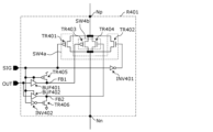
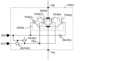
- FIG. 7 shows the configuration of the variable resistor R401, which shows a third modification of the variable resistor R102 in FIG.
- the switch SW1 of FIG. 2 is replaced by the switch SW4a composed of the P-type MOS transistor TR401 and the N-type MOS transistor TR402, and the resistor R103 is switched by the control signal SIG and the voltage VOUT of the output terminal OUT to switch the P-type MOS transistor TR403 and the N-type MOS transistor TR404. It is replaced with a switch SW4b that is used by switching.
- the resistance values in the on state of the switches SW4a and SW4b are assumed to be resistance values Ron4 and Ron4, respectively.
- RPon4 and RNon4 be the on-state resistance values of the P-type MOS transistor TR403 and the N-type MOS transistor TR404 of the switch SW4b, respectively, and let
- BUF401 and BUF402 are buffer circuits that logically output Hiz or voltage VOUT to node FB1 or node FB2 according to control signal SIG and voltage VOUT of output terminal OUT.
- INV401 and INV402 are inverters for inverting the logic of the control signal SIG.
- FIG. 8 is a circuit diagram of the buffer circuits BUF401 and BUF402.
- the buffer circuits BUF401 and BUF402 receive the control signal SIG and the voltage VOUT of the output terminal OUT, and logically output to the node FB1 or FB2.
- BUF501 is a buffer circuit
- TR501 and TR502 are a P-type MOS transistor and an N-type MOS transistor for controlling the power supply of the buffer circuit BUF501
- INV501 is an inverter for logically inverting a control signal.
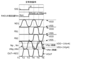
- FIG. 9 shows operation waveforms of the buffer circuit BUF101 during steady oscillation in the oscillation circuit 100.
- FIG. The operation of the buffer circuit BUF101 and the variable resistor R401 will be described using the operation waveforms of FIG. 9 and FIGS. 1 and 6 to 8.
- FIG. 9 shows operation waveforms of the buffer circuit BUF101 during steady oscillation in the oscillation circuit 100.
- FIG. 9 The operation of the buffer circuit BUF101 and the variable resistor R401 will be described using the operation waveforms of FIG. 9 and FIGS. 1 and 6 to 8.
- the P-type MOS transistor TR403 of the variable resistor R401 has its drain grounded, so it acts as a clamp circuit, and the voltage VNp extends from VDD to VSS+
- the P-type MOS transistor TR103 is turned on weakly, and the voltage VOUT of the output terminal OUT (node ND2) transitions from "VSS" to "VDD".
- the output terminal OUT transitions from "VSS" to "VDD", so that the P-type MOS transistor TR403 is turned off, the N-type MOS transistor TR404 is turned on, and the voltage VNp becomes VSS+.
- to VSS with the time constant ⁇ f set by the resistance value Rm the P-type MOS transistor TR103 of the inverter INV103 is turned on.
- the voltage VOUT of the output terminal OUT (node ND2) transitions to "VDD".
- the time constant ⁇ f is set by the resistance value RPon4 of the P-type MOS transistor TR403 in the first stage and by the resistance value RNon4 of the N-type MOS transistor TR404 in the second stage.
- the gate voltage of the P-type MOS transistor TR103 of the inverter INV103 is transitioned in two stages using the voltage clamping characteristics of the variable resistor R401, whereby the through current from the P-type MOS transistor TR103 to the N-type MOS transistor.
- the supply current to the vibrator 101 is suppressed, and the margin of the excitation level can be expanded.
- the logic transition of the voltage VNn of the node Nn in two stages is as follows.
- the N-type MOS transistor TR404 of the variable resistor R401 has its drain grounded, so it acts as a clamp circuit, and the voltage VNn is changed from VSS to VDD-
- the output terminal OUT transitions from "VDD” to "VSS", thereby turning off the N-type MOS transistor TR404 and turning on the P-type MOS transistor TR403, so that the voltage VNn becomes VDD.
- the N-type MOS transistor TR104 of the inverter INV103 is turned on.
- the voltage VOUT of the output terminal OUT transitions to "VSS".
- the time constant ⁇ r is set by the resistance value RNon4 of the N-type MOS transistor TR404 in the first stage and by the resistance value RPon4 of the P-type MOS transistor TR403 in the second stage.
- the buffer circuit BUF101 of the oscillation circuit 100 is connected between the node Np and the node Nn, and according to the control signal and the output of the inverter INV103 at the stage after the inverter INV102, A resistance circuit is provided for logically transitioning the voltage of the node Np or the node Nn in two stages.
- the resistor circuit has a clamp circuit and a switch that short-circuits the clamp circuit.
- a clamp circuit is generated by the source follower voltage of the transistor.
- the input voltage of the inverter INV103 is logically transitioned in two stages, thereby suppressing the current consumption due to the through current of the inverter INV103 and the power supply voltage VDD generated at the time of the logic transition of the inverter INV103. variation and deterioration of EMI characteristics can be suppressed. Furthermore, the supply current to the vibrator 101 is suppressed, and the margin of the excitation level can be expanded.
- clamp circuit of the variable resistor R401 shown in FIG. 7 need not be limited to grounding the drain of the transistor, and a parallel connection of a diode and a transistor or the like may be used to realize a similar function.
- the clamp circuit of the variable resistor R401 can be controlled by connecting the gate of the P-type MOS transistor TR403 and the gate of the N-type MOS transistor TR404 in common, as shown in FIG. can.
- variable resistor R102 including resistors and switches between the nodes Np and Nn shown in FIG.
- the oscillator circuit of the present disclosure achieves good start-up characteristics, current consumption, low EMI, and operational stability of the oscillation operation, and is useful for extending the battery life of mobile phones and battery-driven equipment.
- Oscillator circuit 101 Oscillator C101, C102 Load capacitance A1 Amplifier circuit SIG Control signals INV101, INV102, INV103 Inverter BUF101 Buffer circuit R101 Feedback resistor R102 Variable resistor R103 Resistor SW1 Switch TR101, TR103, TR105 P-type MOS transistor TR102, TR104, TR106 N-type MOS transistor INV104 Inverters SW2a, SW2b, SW3a, SW3b Switches TR201, TR203, TR301, TR303 P-type MOS transistors TR202, TR204, TR302, TR304 N-type MOS transistor R401 Variable resistors SW4a, SW4b Switches TR401, TR403, TR405, TR501 P-type MOS transistors TR402, TR404, TR406, TR502 N-type MOS transistors BUF401, BUF402 Buffer circuit BUF501 Buffer circuit
Landscapes
- Engineering & Computer Science (AREA)
- Power Engineering (AREA)
- Oscillators With Electromechanical Resonators (AREA)
Abstract
Description
図3Aを用いて、起動時の発振回路100の動作を説明する。
時間T1において、制御信号SIGを『L』に設定する。これにより、可変抵抗R102のP型MOSトランジスタTR105及びN型MOSトランジスタTR106がオン状態となり、ノードNpとノードNnとの間の抵抗値RnはスイッチSW1の低抵抗Ronに設定される。また入力端子INに接続されたインバータINV101のDCバイアスVIN_dcは、出力端子OUTの電圧VOUTが帰還抵抗R101を介してフィードバックされることで、おおよそ(VDD/2)となる。
入力端子INの電圧VINは、振動子101が生成した微弱電圧α1・sin(ωt)と入力端子INのDCバイアスVIN_dcとにより、VIN=(VDD/2+α1×sin(ωt))・・・(1)となる。ここで、α1は数μVから数十μVの振幅電圧、ωt=0°から180°間の値とし、sin(ωt)≧0とする。
VNp_dc=VDD×[(Ron+RNinv)/(RPinv+Ron+RNinv)]・・・(3)
VNn_dc=VDD×[(RNinv)/(RPinv+Ron+RNinv)]・・・(4)
VNp=VNp_dc+α1×K1×K2×sin(ωt-(θ1+θ2))・・・(5)
VNn=VNn_dc+α1×K1×K2×sin(ωt-(θ1+θ2))・・・(6)
となる。
VNp=2v+α1×K1×K2×sin(ωt-(θ1+θ2))・・・(7)
VNn=1v+α1×K1×K2×sin(ωt-(θ1+θ2))・・・(8)
となる。ここで、式(7)と式(8)とにより、VNpあるいはVNnを入力とするインバータINV103のP型MOSトランジスタTR103及びN型MOSトランジスタTR104のゲート-ソース間電圧Vgsを、それぞれ1vを中心にしたVgsに設定することが可能となり、インバータINV103を駆動することが可能となる。低抵抗Ronを小さくすることで、更にVgsを大きく設定できる。したがって、振動子が生成する起動時の微小電圧においても、トランジスタをオン状態に出来ることが分かる。
|VDD-VNp|>|Vtp1|・・・(9)
VNn>Vtn1・・・(10)
Ron≦RPinv、かつ、Ron≦RNinv・・・(11)
とすることが望ましいが、式(9)と式(10)とを満たすRonに設定されていれば良い。
振動子101が生成した微小電圧α2×sin(ωt)と入力端子INのDCバイアスVIN_dcにより、入力端子INの電圧VINは、VIN=(VDD/2+α2×sin(ωt))となる。これにより、増幅回路A1は、[時間T1~T2]と同様の動作を繰り返し、出力端子OUTに出力電圧VOUTとして、VOUT=(VDD/2―α2×K1×K2×K3×sin(ωt-(θ1+θ2+θ3)))を出力する。出力電圧VOUTが振動子101にフィードバックされることで、振動子は微小振幅α3×sin(ωt)を生成する。ここで、α3>α2、360°≦ωt≦~540°とする。
Ron≦Rdp、かつ、Ron≦Rdn・・・(12)
が満足されていれば良い。式(12)を満足するノードNp及びノードNnのそれぞれの電圧VNp及びVNn、並びに、インバータINV103の各トランジスタとの関係を示す式(9)と(10)を満たすRonに設定されていれば良い。
次に図3Bを用いて、定常発振時の発振回路100の回路動作を説明する。
制御信号SIGは『L』であり、可変抵抗R102の抵抗値RnはスイッチSW1の低抵抗Ronに設定されている。また入力端子INに接続されたインバータINV101のDCバイアスVIN_dcは、出力端子OUTの電圧VOUTが帰還抵抗R101を介してフィードバックされることで、おおよそ(VDD/2)となる。
まず、入力端子INの電圧VINは、振動子101が生成した電圧αn×sin(ωt)と入力端子INのDCバイアスVIN_dcにより、VIN=(VDD/2+αn×sin(ωt))となる。インバータINV101は、電圧VINを入力とし、ノードND1に電圧VND1として、VND1=VDD/2-αn×K1・sin(ωt-θn)、を出力する。ここで、電圧VND1の振幅電圧αn×K1は、(αn×K1)>>(VDD-VSS)であるとする。これにより、電圧VND1は電源電圧VDD-グランドVSS間で振幅する。よって、ノードND1の電圧VND1は、VND1=VSSとなる。なお、θnはインバータINV101の論理反転時の正の値の遅延成分である。
入力端子INの電圧VINは、振動子101が生成した電圧αn×sin(ωt)と入力端子INのDCバイアスVIN_dcにより、VIN=(VDD/2+αn・sin(ωt))となる。インバータINV101にはVINが入力され、インバータINV101はノードND1に電圧VND1=VDD/2-αn×K1×sin(ωt-θn)、を出力する。ここで、電圧VND1は電源電圧VDD-グランドVSS間で振幅するため、ノードND1の電圧VND1は、VND1=VDDとなる。
時間T5において、制御信号SIGを『L』から『H』に変更する。これにより、可変抵抗R102のP型MOSトランジスタTR105とN型MOSトランジスタTR106とがオフ状態となり、可変抵抗R102の抵抗値Rnは低抵抗値Ronから抵抗R103の高抵抗Rcに切り替わる。これ以降、制御信号SIGが『L』から『H』に制御されることによって回路動作が切り替わるバッファ回路BUF101の動作について説明する。
ノードND1の電圧VND1がVDDからVSSに遷移し、インバータINV102に入力される。これによってインバータINV102のN型MOSトランジスタTR102はオフ状態、P型MOSトランジスタTR101がオン状態となる。
時間T6~T7において、ノードND1の電圧VND1がVSSからVDDに遷移し、インバータINV102に入力される。これによってインバータINV102のP型MOSトランジスタTR101はオフ状態、N型MOSトランジスタTR102がオン状態となる。
図4は本開示の第1の実施の形態の可変抵抗R102の変形例1を示すものであり、図2のスイッチSW1をスイッチSW2aとスイッチSW2bとの直列接続に置き換えたものである。制御信号SIGは制御信号SIGAと制御信号SIGBとから成り、INV201は制御信号SIGAを論理反転するインバータ、INV202は制御信号SIGBを論理反転するインバータ、SW2aはP型MOSトランジスタTR201とN型MOSトランジスタTR202とから成るスイッチ、SW2bはP型MOSトランジスタTR203とN型MOSトランジスタTR204とから成るスイッチ、R201とR202とは抵抗、Nrは抵抗R201とR202間のノードである。
制御信号SIGA=Lの時、P型MOSトランジスタTR201とN型MOSトランジスタTR202とはオン状態となり、ノードNpとノードNrとの間の抵抗値Rn1はスイッチSW2aの抵抗値Ron1となる。一方、制御信号SIGA=Hの時、抵抗値Rn1は抵抗値Rc1となる。
制御信号SIGB=Lの時、P型MOSトランジスタTR203とN型MOSトランジスタTR204とはオン状態となり、ノードNrとノードNnとの間の抵抗値Rn2はスイッチSW2bの抵抗値Ron2となる。一方、制御信号SIGB=Hの時、抵抗値Rn2は抵抗値Rc2となる。
図5は本開示の第1の実施の形態の可変抵抗R102の変形例2を示すものであり、図2のスイッチSW1をスイッチSW3a、抵抗R103をスイッチSW3b、に置き換えている。制御信号SIGは制御信号SIGAと制御信号SIGBから成り、INV301は制御信号SIGAを論理反転するインバータ、INV302は制御信号SIGBを論理反転するインバータ、SW3aはP型MOSトランジスタTR301とN型MOSトランジスタTR302とから成るスイッチ、SW3bはP型MOSトランジスタTR303とN型MOSトランジスタTR304とから成るスイッチ、である。
制御信号SIGA=Lの時、P型MOSトランジスタTR301とN型MOSトランジスタTR302とはオン状態となり、スイッチSW3aの抵抗値はRon1となる。ここで、抵抗値Ron1はP型MOSトランジスタTR301とN型MOSトランジスタTR302との合成オン抵抗である。制御信号SIGA=Hの時、スイッチSW3aはオフ状態となる。
制御信号SIGB=Lの時、P型MOSトランジスタTR303とN型MOSトランジスタTR304とはオン状態となり、スイッチSW3bの抵抗値はRon2となる。ここで、抵抗値Ron2はP型MOSトランジスタTR303とN型MOSトランジスタTR304の合成オン抵抗である。制御信号SIGB=Hの時、スイッチSW3bはオフ状態となる。
図6は本開示の第1の実施の形態のバッファ回路BUF101の変形例1を示すものであり、図1の可変抵抗R102を、制御信号SIGとノードND2の電圧VOUTによって制御される可変抵抗R401、に置き換えている。ここで、ノードND2と出力端子OUTは同電位であり電圧VOUT、可変抵抗R401は抵抗値Rmであるとする。
制御信号SIG=Lにおいて、P型MOSトランジスタTR401とN型MOSトランジスタTR402とはオン状態となる。一方、ノードFB1はP型MOSトランジスタTR405によりVDD、ノードFB2はN型MOSトランジスタTR406によりVSSとなり、P型MOSトランジスタTR403とN型MOSトランジスタTR404とはオフ状態となる。これより、可変抵抗R401の抵抗値RmはスイッチSW4aの抵抗値Ron4となる。抵抗値Ron4が式(11)または式(12)を満足することで、発振回路100は安定的に発振動作を行う。
制御信号SIGが『L』から『H』に遷移する。これにより、可変抵抗R401のP型MOSトランジスタTR401とN型MOSトランジスタTR402とはオフ状態となる。一方、バッファ回路BUF401及びBUF402は出力端子OUTの電圧VOUT=VSSをノードFB1及びFB2に出力し、P型MOSトランジスタTR403はオン状態、N型MOSトランジスタTR404はオフ状態となり、可変抵抗R401の抵抗値Rmは抵抗値RPon4となる。
ノードND1の電圧VND1がVSSからVDDに遷移し、インバータINV102のP型MOSトランジスタTR101がオフ状態、N型MOSトランジスタTR102がオン状態となる。これによりノードNnがVDDからVSSに遷移し、N型MOSトランジスタTR104がオフ状態となる。一方、ノードNpの電圧VNpは、可変抵抗R401の抵抗値Rmで設定された時定数τfでVDDからVSSへ遷移すると共に、2段階で論理遷移することで、P型MOSトランジスタTR103をオン状態とする。
ノードND1の電圧VND1がVDDからVSSに遷移し、インバータINV102のP型MOSトランジスタTR101がオン状態、N型MOSトランジスタTR102がオフ状態となる。これによりノードNpがVSSからVDDに遷移し、P型MOSトランジスタTR103がオフ状態となる。一方、ノードNnの電圧VNnは、可変抵抗R401の抵抗値Rmで設定された時定数τrでVSSからVDDへ遷移すると共に、2段階で論理遷移することで、N型MOSトランジスタTR104をオン状態とする。
101 振動子
C101、C102 負荷容量
A1 増幅回路
SIG 制御信号
INV101、INV102、INV103 インバータ
BUF101 バッファ回路
R101 帰還抵抗
R102 可変抵抗
R103 抵抗
SW1 スイッチ
TR101、TR103、TR105 P型MOSトランジスタ
TR102、TR104、TR106 N型MOSトランジスタ
INV104 インバータ
SW2a、SW2b、SW3a、SW3b スイッチ
TR201、TR203、TR301、TR303 P型MOSトランジスタ
TR202、TR204、TR302、TR304 N型MOSトランジスタ
R401 可変抵抗
SW4a、SW4b スイッチ
TR401、TR403、TR405、TR501 P型MOSトランジスタ
TR402、TR404、TR406、TR502 N型MOSトランジスタ
BUF401、BUF402 バッファ回路
BUF501 バッファ回路
Claims (15)
- 振動子と、
前記振動子の電圧を増幅する増幅回路と、
を備える発振回路であって、
前記増幅回路は、
第1の入力信号を第1のノードと第2のノードとに出力する第1のインバータと、
前記第1のノードと前記第2のノードとの信号を入力として、第3のノードに出力信号を出力する第2のインバータと、
を備え、
前記増幅回路は、更に、
前記第1のノードと前記第2のノードとの間に接続され、制御信号によって制御される可変抵抗を有する
ことを特徴とする発振回路。 - 前記可変抵抗は、
第1の抵抗と、
前記第1の抵抗を短絡するスイッチと、
を有することを特徴とする請求項1に記載の発振回路。 - 前記可変抵抗は、
トランジスタのサイズ比であるゲート長に対するゲート幅の比が異なる複数のトランジスタを含む
ことを特徴とする請求項1に記載の発振回路。 - 前記可変抵抗の抵抗値は、多段階で切り替え可能である
ことを特徴とする請求項1から請求項3のいずれか1項に記載の発振回路。 - 前記可変抵抗の抵抗値は、前記制御信号によって、前記発振回路の起動時と定常発振時とで、切り替えられる
ことを特徴とする請求項1から請求項4のいずれか1項に記載の発振回路。 - 前記可変抵抗の抵抗値は、前記制御信号によって、
前記発振回路の起動時において、前記発振回路の定常発振時より低くなるように切り替えられる
ことを特徴とする請求項1から請求項5のいずれか1項に記載の発振回路。 - 振動子と
前記振動子の電圧を増幅する増幅回路と、
を備える発振回路であって、
前記増幅回路は、
第1の入力信号を第1のノードと第2のノードとに出力する第1のインバータと、
前記第1のノードと前記第2のノードとの信号を入力として、第3のノードに出力信号を出力する第2のインバータと
を備え、
前記増幅回路は、更に、
前記第1のノードと前記第2のノードとの間に電位差を生成する電位差生成回路であって、制御信号によって前記電位差が切り替えられる電位差生成回路を有する
ことを特徴とする発振回路。 - 前記電位差生成回路が、
抵抗及び前記抵抗を短絡するスイッチから成る可変抵抗を含み、
前記制御信号に応じて、前記スイッチを切り替える
ことを特徴とする請求項7に記載の発振回路。 - 前記電位差生成回路が、
トランジスタのサイズ比であるゲート長に対するゲート幅の比が異なる複数のトランジスタを含み、
前記制御信号に応じて、前記複数のトランジスタを切り替える
ことを特徴とする請求項7に記載の発振回路。 - 前記電位差生成回路は、
抵抗及びトランジスタの両方あるいは一方を含む抵抗回路から成り、
前記第1のインバータは、
複数の電流を設定可能な電流調整回路を備え、
前記制御信号に応じて、前記電流調整回路を切り替える
ことを特徴とする請求項7に記載の発振回路。 - 振動子と
前記振動子の電圧を増幅する増幅回路と、
を備える発振回路であって、
前記増幅回路は、
第1の入力信号を第1のノードと第2のノードとに出力する第1のインバータと、
前記第1のノードと前記第2のノードとの信号を入力として、第3のノードに出力信号を出力する第2のインバータと、
を備え、
前記増幅回路は、更に、
前記第1のノードと前記第2のノードとの間に接続され、制御信号と、前記第1のインバータより後段のインバータの出力と、に応じて、前記第1のノードまたは前記第2のノードの電圧を2段階で論理遷移させる抵抗回路を備える
ことを特徴とする発振回路。 - 前記抵抗回路は、
クランプ回路と、
前記クランプ回路を短絡するスイッチと、
を有することを特徴とする請求項11に記載の発振回路。 - クランプ回路は、トランジスタのソースフォロワー電圧により生成される
ことを特徴とする請求項12に記載の発振回路。 - 第1の入力信号を第1のノードと第2のノードとに出力する第1のインバータと、
前記第1のノードと前記第2のノードとの信号を入力として、第3のノードに出力信号を出力する第2のインバータと、
を備え、
更に、
前記第1のノードと前記第2のノードとの間に電位差を生成する電位差生成回路であって、制御信号によって、前記電位差が切り替えられる電位差生成回路を有する
ことを特徴とするバッファ回路。 - 第1の入力信号を第1のノードと第2のノードとに出力する第1のインバータと、
前記第1のノードと前記第2のノードとの信号を入力として、第3のノードに出力信号を出力する第2のインバータと、
を備え、更に、
前記第1のノードと前記第2のノードとの間に接続され、制御信号と、前記第1のインバータより後段のインバータの出力と、に応じて、前記第1のノードまたは前記第2のノードの電圧を、2段階で論理遷移させる抵抗回路を備える
ことを特徴とする発振回路。
Priority Applications (3)
| Application Number | Priority Date | Filing Date | Title |
|---|---|---|---|
| CN202380022008.5A CN118715710A (zh) | 2022-02-24 | 2023-02-10 | 振荡电路及缓冲电路 |
| JP2024503026A JPWO2023162736A1 (ja) | 2022-02-24 | 2023-02-10 | |
| US18/807,346 US12476591B2 (en) | 2022-02-24 | 2024-08-16 | Oscillator circuit and buffer circuit |
Applications Claiming Priority (2)
| Application Number | Priority Date | Filing Date | Title |
|---|---|---|---|
| JP2022-027099 | 2022-02-24 | ||
| JP2022027099 | 2022-02-24 |
Related Child Applications (1)
| Application Number | Title | Priority Date | Filing Date |
|---|---|---|---|
| US18/807,346 Continuation US12476591B2 (en) | 2022-02-24 | 2024-08-16 | Oscillator circuit and buffer circuit |
Publications (1)
| Publication Number | Publication Date |
|---|---|
| WO2023162736A1 true WO2023162736A1 (ja) | 2023-08-31 |
Family
ID=87765842
Family Applications (1)
| Application Number | Title | Priority Date | Filing Date |
|---|---|---|---|
| PCT/JP2023/004668 Ceased WO2023162736A1 (ja) | 2022-02-24 | 2023-02-10 | 発振回路、及びバッファ回路 |
Country Status (5)
| Country | Link |
|---|---|
| US (1) | US12476591B2 (ja) |
| JP (1) | JPWO2023162736A1 (ja) |
| CN (1) | CN118715710A (ja) |
| TW (1) | TW202341641A (ja) |
| WO (1) | WO2023162736A1 (ja) |
Citations (5)
| Publication number | Priority date | Publication date | Assignee | Title |
|---|---|---|---|---|
| JPH0470101A (ja) * | 1990-07-10 | 1992-03-05 | Fujitsu Ltd | 半導体集積回路装置 |
| JPH05145341A (ja) * | 1991-11-20 | 1993-06-11 | Citizen Watch Co Ltd | 水晶発振器 |
| JP2005210403A (ja) * | 2004-01-22 | 2005-08-04 | Asahi Kasei Microsystems Kk | 出力バッファ回路 |
| US20080116952A1 (en) * | 2006-11-17 | 2008-05-22 | Kiyoshi Kase | Latching input buffer circuit with variable hysteresis |
| JP2012205141A (ja) * | 2011-03-25 | 2012-10-22 | Toshiba Corp | スイッチング回路 |
Family Cites Families (2)
| Publication number | Priority date | Publication date | Assignee | Title |
|---|---|---|---|---|
| JP6111085B2 (ja) | 2013-02-13 | 2017-04-05 | セイコーNpc株式会社 | 発振用集積回路 |
| US11329608B1 (en) * | 2020-10-23 | 2022-05-10 | Infineon Technologies Ag | Oscillator circuit with negative resistance margin testing |
-
2023
- 2023-02-10 TW TW112104774A patent/TW202341641A/zh unknown
- 2023-02-10 WO PCT/JP2023/004668 patent/WO2023162736A1/ja not_active Ceased
- 2023-02-10 CN CN202380022008.5A patent/CN118715710A/zh active Pending
- 2023-02-10 JP JP2024503026A patent/JPWO2023162736A1/ja active Pending
-
2024
- 2024-08-16 US US18/807,346 patent/US12476591B2/en active Active
Patent Citations (5)
| Publication number | Priority date | Publication date | Assignee | Title |
|---|---|---|---|---|
| JPH0470101A (ja) * | 1990-07-10 | 1992-03-05 | Fujitsu Ltd | 半導体集積回路装置 |
| JPH05145341A (ja) * | 1991-11-20 | 1993-06-11 | Citizen Watch Co Ltd | 水晶発振器 |
| JP2005210403A (ja) * | 2004-01-22 | 2005-08-04 | Asahi Kasei Microsystems Kk | 出力バッファ回路 |
| US20080116952A1 (en) * | 2006-11-17 | 2008-05-22 | Kiyoshi Kase | Latching input buffer circuit with variable hysteresis |
| JP2012205141A (ja) * | 2011-03-25 | 2012-10-22 | Toshiba Corp | スイッチング回路 |
Also Published As
| Publication number | Publication date |
|---|---|
| US12476591B2 (en) | 2025-11-18 |
| US20240405720A1 (en) | 2024-12-05 |
| JPWO2023162736A1 (ja) | 2023-08-31 |
| CN118715710A (zh) | 2024-09-27 |
| TW202341641A (zh) | 2023-10-16 |
Similar Documents
| Publication | Publication Date | Title |
|---|---|---|
| US7915966B2 (en) | Oscillator for controlling voltage | |
| US20110057736A1 (en) | Linear, Voltage-Controlled Ring Oscillator With Current-Mode, Digital Frequency And Gain Control | |
| US20120075025A1 (en) | Oscillating circuit | |
| US5469116A (en) | Clock generator circuit with low current frequency divider | |
| KR20090034360A (ko) | 다기능 및 콤팩트 dc―결합 cml 버퍼 | |
| JP7751271B2 (ja) | 発振回路および電子機器 | |
| KR100996386B1 (ko) | 반도체 회로 | |
| US9634608B2 (en) | Crystal oscillation circuit and electronic timepiece | |
| US20080238561A1 (en) | Piezoelectric oscillator | |
| US6611177B2 (en) | Voltage controlled oscillator including fluctuation transmitter for transmitting potential fluctuation by noise | |
| US6211699B1 (en) | High performance CML to CMOS converter | |
| US20070052459A1 (en) | Multiphased triangular wave oscillating circuit and switching regulator using it | |
| EP1488516B1 (en) | CMOS inverter circuit | |
| WO2023162736A1 (ja) | 発振回路、及びバッファ回路 | |
| US7511584B2 (en) | Voltage controlled oscillator capable of operating in a wide frequency range | |
| US7679465B2 (en) | Oscillator circuit | |
| JPH1098356A (ja) | 電圧制御発振器 | |
| US20060232346A1 (en) | Integrated circuit including a ring oscillator circuit | |
| US7321270B2 (en) | Current-controlled CMOS ring oscillator circuit | |
| US6828868B2 (en) | Semiconductor device having an oscillating circuit | |
| JPWO2023162736A5 (ja) | ||
| JP2007053746A (ja) | 集積回路 | |
| CN113612447B (zh) | 一种振荡电路 | |
| US20240333214A1 (en) | Oscillation circuit and semiconductor integrated circuit | |
| WO2010126487A1 (en) | Linear, voltage-controlled ring oscillator with current-mode, digital frequency and gain control |
Legal Events
| Date | Code | Title | Description |
|---|---|---|---|
| 121 | Ep: the epo has been informed by wipo that ep was designated in this application |
Ref document number: 23759740 Country of ref document: EP Kind code of ref document: A1 |
|
| ENP | Entry into the national phase |
Ref document number: 2024503026 Country of ref document: JP Kind code of ref document: A |
|
| WWE | Wipo information: entry into national phase |
Ref document number: 202380022008.5 Country of ref document: CN |
|
| NENP | Non-entry into the national phase |
Ref country code: DE |
|
| 122 | Ep: pct application non-entry in european phase |
Ref document number: 23759740 Country of ref document: EP Kind code of ref document: A1 |