WO2023157136A1 - 配線基板の製造方法、配線基板、レチクル、及び、露光描画データ構造 - Google Patents
配線基板の製造方法、配線基板、レチクル、及び、露光描画データ構造 Download PDFInfo
- Publication number
- WO2023157136A1 WO2023157136A1 PCT/JP2022/006209 JP2022006209W WO2023157136A1 WO 2023157136 A1 WO2023157136 A1 WO 2023157136A1 JP 2022006209 W JP2022006209 W JP 2022006209W WO 2023157136 A1 WO2023157136 A1 WO 2023157136A1
- Authority
- WO
- WIPO (PCT)
- Prior art keywords
- wiring
- exposure pattern
- dummy
- metal
- resist layer
- Prior art date
- Legal status (The legal status is an assumption and is not a legal conclusion. Google has not performed a legal analysis and makes no representation as to the accuracy of the status listed.)
- Ceased
Links
Images





Classifications
-
- H—ELECTRICITY
- H05—ELECTRIC TECHNIQUES NOT OTHERWISE PROVIDED FOR
- H05K—PRINTED CIRCUITS; CASINGS OR CONSTRUCTIONAL DETAILS OF ELECTRIC APPARATUS; MANUFACTURE OF ASSEMBLAGES OF ELECTRICAL COMPONENTS
- H05K1/00—Printed circuits
- H05K1/02—Details
- H05K1/0296—Conductive pattern lay-out details not covered by sub groups H05K1/02 - H05K1/0295
-
- G—PHYSICS
- G03—PHOTOGRAPHY; CINEMATOGRAPHY; ANALOGOUS TECHNIQUES USING WAVES OTHER THAN OPTICAL WAVES; ELECTROGRAPHY; HOLOGRAPHY
- G03F—PHOTOMECHANICAL PRODUCTION OF TEXTURED OR PATTERNED SURFACES, e.g. FOR PRINTING, FOR PROCESSING OF SEMICONDUCTOR DEVICES; MATERIALS THEREFOR; ORIGINALS THEREFOR; APPARATUS SPECIALLY ADAPTED THEREFOR
- G03F1/00—Originals for photomechanical production of textured or patterned surfaces, e.g., masks, photo-masks, reticles; Mask blanks or pellicles therefor; Containers specially adapted therefor; Preparation thereof
- G03F1/38—Masks having auxiliary features, e.g. special coatings or marks for alignment or testing; Preparation thereof
-
- H—ELECTRICITY
- H05—ELECTRIC TECHNIQUES NOT OTHERWISE PROVIDED FOR
- H05K—PRINTED CIRCUITS; CASINGS OR CONSTRUCTIONAL DETAILS OF ELECTRIC APPARATUS; MANUFACTURE OF ASSEMBLAGES OF ELECTRICAL COMPONENTS
- H05K3/00—Apparatus or processes for manufacturing printed circuits
-
- H—ELECTRICITY
- H05—ELECTRIC TECHNIQUES NOT OTHERWISE PROVIDED FOR
- H05K—PRINTED CIRCUITS; CASINGS OR CONSTRUCTIONAL DETAILS OF ELECTRIC APPARATUS; MANUFACTURE OF ASSEMBLAGES OF ELECTRICAL COMPONENTS
- H05K3/00—Apparatus or processes for manufacturing printed circuits
- H05K3/02—Apparatus or processes for manufacturing printed circuits in which the conductive material is applied to the surface of the insulating support and is thereafter removed from such areas of the surface which are not intended for current conducting or shielding
- H05K3/06—Apparatus or processes for manufacturing printed circuits in which the conductive material is applied to the surface of the insulating support and is thereafter removed from such areas of the surface which are not intended for current conducting or shielding the conductive material being removed chemically or electrolytically, e.g. by photo-etch process
-
- H—ELECTRICITY
- H05—ELECTRIC TECHNIQUES NOT OTHERWISE PROVIDED FOR
- H05K—PRINTED CIRCUITS; CASINGS OR CONSTRUCTIONAL DETAILS OF ELECTRIC APPARATUS; MANUFACTURE OF ASSEMBLAGES OF ELECTRICAL COMPONENTS
- H05K3/00—Apparatus or processes for manufacturing printed circuits
- H05K3/10—Apparatus or processes for manufacturing printed circuits in which conductive material is applied to the insulating support in such a manner as to form the desired conductive pattern
- H05K3/18—Apparatus or processes for manufacturing printed circuits in which conductive material is applied to the insulating support in such a manner as to form the desired conductive pattern using precipitation techniques to apply the conductive material
-
- H—ELECTRICITY
- H05—ELECTRIC TECHNIQUES NOT OTHERWISE PROVIDED FOR
- H05K—PRINTED CIRCUITS; CASINGS OR CONSTRUCTIONAL DETAILS OF ELECTRIC APPARATUS; MANUFACTURE OF ASSEMBLAGES OF ELECTRICAL COMPONENTS
- H05K3/00—Apparatus or processes for manufacturing printed circuits
- H05K3/10—Apparatus or processes for manufacturing printed circuits in which conductive material is applied to the insulating support in such a manner as to form the desired conductive pattern
- H05K3/18—Apparatus or processes for manufacturing printed circuits in which conductive material is applied to the insulating support in such a manner as to form the desired conductive pattern using precipitation techniques to apply the conductive material
- H05K3/188—Apparatus or processes for manufacturing printed circuits in which conductive material is applied to the insulating support in such a manner as to form the desired conductive pattern using precipitation techniques to apply the conductive material by direct electroplating
-
- H—ELECTRICITY
- H05—ELECTRIC TECHNIQUES NOT OTHERWISE PROVIDED FOR
- H05K—PRINTED CIRCUITS; CASINGS OR CONSTRUCTIONAL DETAILS OF ELECTRIC APPARATUS; MANUFACTURE OF ASSEMBLAGES OF ELECTRICAL COMPONENTS
- H05K2201/00—Indexing scheme relating to printed circuits covered by H05K1/00
- H05K2201/09—Shape and layout
- H05K2201/09209—Shape and layout details of conductors
- H05K2201/09654—Shape and layout details of conductors covering at least two types of conductors provided for in H05K2201/09218 - H05K2201/095
- H05K2201/09781—Dummy conductors, i.e. not used for normal transport of current; Dummy electrodes of components
-
- H—ELECTRICITY
- H05—ELECTRIC TECHNIQUES NOT OTHERWISE PROVIDED FOR
- H05K—PRINTED CIRCUITS; CASINGS OR CONSTRUCTIONAL DETAILS OF ELECTRIC APPARATUS; MANUFACTURE OF ASSEMBLAGES OF ELECTRICAL COMPONENTS
- H05K2203/00—Indexing scheme relating to apparatus or processes for manufacturing printed circuits covered by H05K3/00
- H05K2203/01—Tools for processing; Objects used during processing
- H05K2203/0104—Tools for processing; Objects used during processing for patterning or coating
- H05K2203/0121—Patterning, e.g. plating or etching by moving electrode
-
- H—ELECTRICITY
- H05—ELECTRIC TECHNIQUES NOT OTHERWISE PROVIDED FOR
- H05K—PRINTED CIRCUITS; CASINGS OR CONSTRUCTIONAL DETAILS OF ELECTRIC APPARATUS; MANUFACTURE OF ASSEMBLAGES OF ELECTRICAL COMPONENTS
- H05K2203/00—Indexing scheme relating to apparatus or processes for manufacturing printed circuits covered by H05K3/00
- H05K2203/05—Patterning and lithography; Masks; Details of resist
- H05K2203/0562—Details of resist
- H05K2203/0582—Coating by resist, i.e. resist used as mask for application of insulating coating or of second resist
-
- H—ELECTRICITY
- H05—ELECTRIC TECHNIQUES NOT OTHERWISE PROVIDED FOR
- H05K—PRINTED CIRCUITS; CASINGS OR CONSTRUCTIONAL DETAILS OF ELECTRIC APPARATUS; MANUFACTURE OF ASSEMBLAGES OF ELECTRICAL COMPONENTS
- H05K2203/00—Indexing scheme relating to apparatus or processes for manufacturing printed circuits covered by H05K3/00
- H05K2203/07—Treatments involving liquids, e.g. plating, rinsing
- H05K2203/0703—Plating
- H05K2203/0723—Electroplating, e.g. finish plating
Definitions
- the present disclosure relates to a wiring board manufacturing method, a wiring board, a reticle, and an exposure drawing data structure.
- a semi-additive (SAP) method and a modified semi-additive (MSAP) method are widely used as methods for forming a wiring having a very small width (see, for example, Patent Document 1). These methods generally involve forming a copper plating layer on a metal layer by electroplating, the SAP method using an electroless copper plating layer for the metal layer, and the MSAP method using a copper foil.
- An object of the present disclosure is to provide a method of manufacturing a wiring board, a wiring board, a reticle, and an exposure drawing data structure that can suppress yield reduction due to collapse of metal wiring.
- One aspect of the present disclosure relates to a method for manufacturing a wiring board.
- This method of manufacturing a wiring board includes the steps of forming a resist layer on a support, exposing the resist layer, developing the exposed resist layer to form an opening in the resist layer, and forming an opening in the opening.
- the method includes a step of forming metal wiring and a step of removing the resist layer after the metal wiring is formed.
- the wiring exposure pattern corresponding to the metal wiring and the dummy exposure pattern not corresponding to the metal wiring are exposed to the resist layer. At least part of the dummy exposure pattern is positioned within 200 ⁇ m from the edge of the wiring exposure pattern.
- a dummy exposure pattern which does not constitute the wiring etc. of the wiring board is formed in a region within 200 ⁇ m from the end of the wiring exposure pattern corresponding to the metal wiring constituting the wiring etc. of the wiring board. at least partially located.
- a dummy metal structure is provided in the region exposed by the dummy exposure pattern, or the resist layer in the region is divided into small pieces by providing the dummy exposure pattern, so that the area exposed by the wiring exposure pattern is reduced.
- the stress from the resist to the metal wiring provided in the region can be reduced.
- the adjacent dummy exposure pattern can prevent the metal wiring from collapsing due to the stress of the resist during the manufacturing process of the wiring board.
- the metal wiring referred to herein includes, for example, wiring electrodes formed for horizontal electrical connection in a chip or substrate, or terminal electrodes or projecting electrodes formed for vertical electrical connection. is included.
- the resist layer in the step of forming the resist layer, the resist layer is formed on the metal layer provided on the support, and in the step of forming the opening, the metal layer is exposed from the opening, and the metal layer is exposed from the opening.
- finer wiring electrodes can be easily formed by forming metal wiring by SAP method, MSAP method, or the like. Therefore, according to this wiring board manufacturing method, it is possible to realize miniaturization or a reduction in the diameter of wiring electrodes and the like.
- the dummy exposure pattern may surround at least part of the wiring exposure pattern. Also, the dummy exposure pattern may surround the entire wiring exposure pattern.
- the outer side tends to collapse due to the peeling of the resist, but the arrangement of the dummy exposure pattern more reliably suppresses the collapse of the metal wirings, thereby increasing the yield. Decrease can be suppressed.
- the dummy exposure pattern may include a mesh shape in which a plurality of lines are arranged in a grid.
- the dummy exposure pattern can more reliably suppress collapse of the metal wiring such as the wiring electrode due to peeling of the resist, thereby suppressing a decrease in yield.
- the width or diameter of the formed metal wiring in the lateral direction may be 20 ⁇ m or less.
- metal wiring such as wiring electrodes can be made finer or finer, and even when fine or fine metal wiring is provided, it is possible to suppress the falling of the metal wiring and suppress the decrease in yield. can be done.
- the resist layer may be formed of a negative resist, and the resist has a swelling rate of 30 wt. % or less.
- the resist may have a swelling rate of 5% by weight or more, or 10% by weight or more and 20% by weight or less after being immersed in a 10-fold diluted stripping solution at 22° C. for 1 minute.
- the stripping liquid can be a general-purpose stripping liquid.
- the dummy exposure pattern may have a linear portion, and the width of the linear portion may be equal to or less than the resolution of the resist forming the resist layer.
- the exposed resist layer is divided into small pieces, so that it is possible to prevent the metal wiring from falling down when the resist is stripped. Thereby, according to this manufacturing method, it is possible to suppress a decrease in yield.
- this manufacturing method since it is difficult to form a dummy metal structure based on a dummy exposure pattern, it is not necessary to leave unnecessary portions in the manufactured wiring board.
- the resist layer in the step of exposing the resist layer, may be exposed using a reticle including a wiring exposure pattern and a dummy exposure pattern.
- drawing may be performed based on exposure drawing data including the wiring exposure pattern and the dummy exposure pattern, and the resist layer may be exposed.
- a member such as a reticle becomes unnecessary, so the manufacturing cost can be reduced accordingly.
- the exposure drawing data can be easily created or corrected.
- a beam of a laser or an electron gun can be used for exposure.
- the wiring board includes a support, a plurality of metal wires provided on the support, and at least one dummy metal structure surrounding at least a portion of the plurality of metal wires.
- the width or diameter of the metal wiring in the lateral direction is 20 ⁇ m or less, and at least part of the dummy metal structure is located within 200 ⁇ m from the metal wiring closest to the dummy metal structure among the plurality of metal wirings.
- the dummy metal structure is located within 200 ⁇ m from the metal wiring closest to the dummy metal structure among the plurality of metal wirings constituting the wiring of the wiring board.
- the adjacent dummy metal structure can prevent the metal wiring from collapsing due to stress due to expansion of the resist during the manufacturing process of the wiring board. As a result, according to this wiring board, the collapse of the metal wiring is suppressed.
- the dummy metal structures include a mesh-shaped dummy metal structure in which a plurality of lines are arranged in a grid pattern, an inner dummy metal structure positioned between the plurality of metal lines, and a plurality of metal lines arranged in a line. and a dummy metal structure having a plurality of dot-shaped electrodes surrounding at least a portion of the plurality of metal wires.
- the planar shape of the dot-shaped electrodes may have, for example, geometric patterns such as circles, triangles, squares, cross marks, and combinations thereof.
- the present disclosure provides a reticle for exposing a resist.
- This reticle includes a wiring exposure pattern and a dummy exposure pattern at least a part of which is located within 200 ⁇ m from the end of the wiring exposure pattern.
- the wiring etc. in the wiring board are not formed in the area within 200 ⁇ m from the end of the wiring exposure pattern corresponding to the metal wiring constituting the wiring etc. in the wiring board.
- At least part of the dummy exposure pattern can be located.
- the adjacent dummy exposure pattern prevents the metal wiring from collapsing due to the stress caused by the expansion of the resist during the manufacturing process of the wiring board, thereby suppressing the yield reduction of the wiring board. be able to.
- the dummy exposure pattern may be formed so as to surround at least part of the wiring exposure pattern. In this case, such arrangement of the dummy exposure pattern can more reliably suppress the collapse of the metal wiring, thereby suppressing a decrease in the yield of the wiring board.
- the present disclosure provides an exposure drawing data structure for an exposure apparatus for exposing a resist layer.
- This exposure drawing data structure includes wiring exposure data that causes the exposure device to draw a wiring exposure pattern and dummy exposure data that causes the exposure device to draw a dummy exposure pattern. and dummy exposure data located within 200 ⁇ m from the end of the pattern.
- wiring electrodes, etc., on the wiring board are configured within 200 ⁇ m from the end of the wiring exposure pattern corresponding to the metal wiring that constitutes the wiring, etc. on the wiring board.
- At least a portion of the dummy exposure pattern may be positioned that is not intended to be used. As a result, it is possible to prevent the metal wiring from falling down during the manufacturing process of the wiring board by means of the adjacent dummy exposure pattern, thereby suppressing a decrease in the yield of the wiring board.
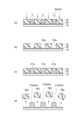
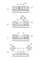
- FIG. 1 is a cross-sectional view showing an example of a method for manufacturing a wiring board according to one embodiment of the present invention.
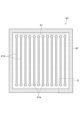
- FIG. 2 is a plan view showing an example of a pattern exposed in the exposure step in the wiring board manufacturing method shown in FIG.
- FIG. 3 is an enlarged plan view showing an enlarged corner S of the exposure pattern shown in FIG.
- FIG. 4 is a cross-sectional view showing an example of exposure and development of a region corresponding to a dummy exposure pattern, showing an example in which the line width of the dummy exposure pattern is equal to or greater than the resolution of the resist.
- FIG. 1 is a cross-sectional view showing an example of a method for manufacturing a wiring board according to one embodiment of the present invention.
- FIG. 2 is a plan view showing an example of a pattern exposed in the exposure step in the wiring board manufacturing method shown in FIG.
- FIG. 3 is an enlarged plan view showing an enlarged corner S of the exposure pattern shown in FIG.
- FIG. 4 is a cross-
- FIG. 5 is a cross-sectional view showing an example of exposure and development of a region corresponding to a dummy exposure pattern, showing an example in which the line width of the dummy exposure pattern is smaller than the resolution of the resist.
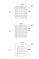
- FIGS. 6A and 6B are diagrams showing examples of exposure patterns with different dummy exposure patterns.
- (a) to (c) of FIG. 7 are diagrams showing examples of exposure patterns with further different dummy exposure patterns.
- FIG. 8 is a diagram showing an exposure pattern according to Example 1.
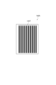
- FIG. FIG. 9 is a diagram showing an exposure pattern according to Comparative Example 1.
- FIG. 10 is a photograph showing wiring electrodes of a wiring board according to Comparative Example 1.
- FIG. FIG. 11 is a cross-sectional view showing a state in which a wiring electrode is tilted due to expansion of a resist in a wiring board manufacturing method.
- the term “layer” includes not only a shape structure formed over the entire surface but also a shape structure formed partially when observed as a plan view.
- the term “process” includes not only an independent process, but also when the intended action of the process is achieved even if it cannot be clearly distinguished from other processes. .
- the numerical range indicated using “-" indicates the range including the numerical values before and after “-" as the minimum and maximum values, respectively.
- the upper limit value or lower limit value of the numerical range at one step may be replaced with the upper limit value or lower limit value of the numerical range at another step.
- the upper or lower limits of the numerical ranges may be replaced with the values shown in the examples.
- (meth)acrylic acid means at least one of “acrylic acid” and “methacrylic acid” corresponding thereto, and the same applies to other similar expressions such as (meth)acrylate.
- FIG. 1 is a diagram showing an example of a wiring board manufacturing method according to an embodiment of the present invention.
- FIG. 2 is a plan view showing an example of a pattern exposed in the exposure step in the wiring board manufacturing method shown in FIG.
- the method for manufacturing the wiring board shown in FIG. 1 includes a step A of forming a metal layer on a support, a step B of forming a resist layer on the metal layer on the support, a step C of exposing the resist layer, A step D of developing the exposed resist layer to form an opening in the resist layer, a step E of forming a metal wiring in the opening, a step F of removing the resist layer after the metal wiring is formed, and a metal wiring. and a step G of removing metal layers other than the above.
- a metal layer 20 is formed on the main surface 10a of a plate-like support 10.
- the outermost layer of the support 10 on which the metal layer 20 is provided is, for example, an insulating layer.
- the insulating layer provided as the outermost layer of the support 10 may be, for example, an insulating resin layer such as a buildup layer.
- the support 10 may include wiring connected to wiring electrodes 2 (see (f) in FIG. 1), which will be described later.
- the metal layer 20 is a layer that functions as a seed layer for electrolytic plating.
- the metal layer 20 may be, for example, a metal plating layer formed by electroless plating, a metal foil such as copper foil, a layer formed by vapor deposition such as sputtering, or a sintered metal layer.
- the sintered metal layer is a layer formed by heating a coating film containing metal particles to sinter the metal particles.
- Metal layer 20 may contain, for example, at least one metal selected from the group consisting of copper, gold, silver, tungsten, molybdenum, tin, cobalt, chromium, iron, titanium, and zinc.
- the metal layer 20 may be a single layer, or may be composed of two or more layers.
- the thickness of the metal layer 20 may be, for example, 0.1-10.0 ⁇ m.
- a resist layer 30 is formed on the metal layer 20 on the support 10, as shown in FIG. 1(b).
- the resist layer 30 can be formed of a photosensitive resist material commonly used for forming wiring.
- the resist material forming the resist layer 30 may be a negative resist material, such as a material containing an acrylic polymer containing carboxylic acid.
- the thickness of the resist layer 30 may be, for example, 5 to 200 ⁇ m.
- a resist material for forming the resist layer 30 may be, for example, a photosensitive resin composition containing a binder polymer, a photopolymerizable compound having an ethylenically unsaturated bond, and a photopolymerization initiator.
- the binder polymer may be, for example, a copolymer containing benzyl (meth)acrylate or its derivative, styrene or a styrene derivative, (meth)acrylic acid alkyl ester, and (meth)acrylic acid as monomer units.
- benzyl (meth)acrylate derivatives constituting the binder polymer include 4-methylbenzyl (meth)acrylate, 4-ethylbenzyl (meth)acrylate, 4-tertbutylbenzyl (meth)acrylate, 4-methoxybenzyl ( meth)acrylate, 4-ethoxybenzyl (meth)acrylate, 4-hydroxybenzyl (meth)acrylate, and 4-chlorobenzyl (meth)acrylate.
- styrene derivatives that make up the binder polymer include vinyltoluene, p-methylstyrene, and p-chlorostyrene.
- the (meth)acrylic acid alkyl ester that constitutes the binder polymer may be an ester compound formed from (meth)acrylic acid and a linear or branched aliphatic alcohol having 1 to 12 carbon atoms.
- the aliphatic alcohol may have 1-8 or 1-4 carbon atoms.
- (meth) acrylic acid alkyl esters include methyl (meth) acrylate, ethyl (meth) acrylate, propyl (meth) acrylate, isopropyl (meth) acrylate, butyl (meth) acrylate, (meth) ) tert-butyl acrylate, pentyl (meth)acrylate, hexyl (meth)acrylate, heptyl (meth)acrylate, octyl (meth)acrylate, and 2-ethylhexyl (meth)acrylate.
- the ratio of monomer units derived from benzyl (meth)acrylate or derivatives thereof in the binder polymer is 50 to 80% by mass, 50 to 75% by mass, 50 to 70% by mass, or 50 to 65% by mass based on the mass of the binder polymer. %.
- the proportion of monomer units derived from styrene or styrene derivatives in the binder polymer may be 5 to 40% by weight, or 5 to 35% by weight based on the weight of the binder polymer.
- the ratio of monomer units derived from (meth)acrylic acid alkyl ester in the binder polymer is 1 to 20% by mass, 1 to 15% by mass, 1 to 10% by mass, or 1 to 5% by mass based on the mass of the binder polymer.
- the proportion of monomer units derived from (meth)acrylic acid in the binder polymer may be 5 to 30% by weight, 5 to 25% by weight, or 10 to 25% by weight based on the weight of the binder polymer.
- the weight average molecular weight (Mw) of the binder polymer may be 20,000 to 150,000, 30,000 to 100,000, 40,000 to 80,000, or 40,000 to 60,000.
- a weight average molecular weight here means a standard polystyrene conversion value calculated
- the acid value (mgKOH/g) of the binder polymer may be 13-78, 39-65, or 52-62.
- the acid value here means the amount (mg) of potassium hydroxide required to neutralize 1 g of the binder polymer.
- photopolymerizable compounds having an ethylenically unsaturated bond include bisphenol A (meth)acrylate compounds, hydrogenated bisphenol A (meth)acrylate compounds, polyalkylene glycol (meth)acrylates, urethane monomers, and pentaerythritol. (meth)acrylates and trimethylolpropane (meth)acrylates. These are used alone or in combination of two or more.
- the bisphenol A-based di(meth)acrylate compound may be, for example, a compound represented by the following general formula (1).
- each R independently represents a hydrogen atom or a methyl group.
- EO and PO represent oxyethylene and oxypropylene groups, respectively.
- m 1 , m 2 , n 1 and n 2 each independently represent 0-40, m 1 +m 2 is 1-40, and n 1 +n 2 is 0-20.
- Either EO or PO may be on the phenolic hydroxyl group side.
- m 1 , m 2 , n 1 and n 2 respectively indicate the number of EOs or POs.
- a compound having m 1 +m 2 of 5 or less on average and a compound having m 1 +m 2 of 6 to 40 on average may be combined.
- the polyalkylene glycol (meth)acrylate may be a compound represented by the following formula (2).
- a bisphenol A-based di(meth)acrylate compound and a compound represented by the following formula (2) may be combined as the photopolymerizable compound having an ethylenically unsaturated bond.
- R 14 and R 15 each independently represent a hydrogen atom or a methyl group
- EO and PO are as defined above
- s 1 represents 1 to 30
- r 1 and r 2 are each 0 ⁇ 30
- r 1 +r 2 is 1-30.
- Commercially available examples of the compound represented by formula ( 2 ) include a vinyl compound ( Showa Denko Materials Co., Ltd., trade name: FA-023M).
- photopolymerization initiators include benzophenone, N,N'-tetramethyl-4,4'-diaminobenzophenone (Michler's ketone), N,N'-tetraethyl-4,4'-diaminobenzophenone, 4-methoxy- 4′-dimethylaminobenzophenone, 2-benzyl-2-dimethylamino-1-(4-morpholinophenyl)-butanone-1,2-methyl-1-[4-(methylthio)phenyl]-2-morpholino-propanone- Aromatic ketones such as 1; 2-ethylanthraquinone, phenanthrenequinone, 2-tert-butylanthraquinone, octamethylanthraquinone, 1,2-benzanthraquinone, 2,3-benzanthraquinone, 2-phenylanthraquinone, 2,3-diphenyl quinones such as an
- the content of the binder polymer in the photosensitive resin composition is 40 to 80 parts by mass, 45 to 75 parts by mass, or 50 to 70 parts by mass with respect to 100 parts by mass as the total amount of the binder polymer and the photopolymerizable compound.
- the content of the photopolymerization initiator in the photosensitive resin composition is 0.01 to 5 parts by mass, 0.1 to 4.5 parts by mass with respect to 100 parts by mass of the total amount of the binder polymer and the photopolymerizable compound, Alternatively, it may be 1 to 4 parts by mass.
- the photosensitive resin composition may contain other components as necessary.
- other components include a photopolymerizable compound having a cationic polymerizable cyclic ether group, a cationic polymerization initiator, a sensitizer, dyes such as malachite green, tribromomethylphenylsulfone, and photocoloring such as leuco crystal violet.
- agents, anti-thermal coloring agents, plasticizers such as p-toluenesulfonamide, pigments, fillers, antifoaming agents, flame retardants, stabilizers, adhesion imparting agents, leveling agents, release accelerators, antioxidants, fragrances, Imaging agents, and thermal cross-linking agents are included.
- the content of other components may be about 0.01 to 20 parts by mass, respectively, with respect to 100 parts by mass of the total amount of the binder polymer and the photopolymerizable compound.
- the total content of the binder polymer, the photopolymerizable compound and the photopolymerization initiator in the photosensitive resin composition is 90 to 100% by mass, or It may be 95 to 100% by mass.
- a resist film containing a photosensitive resin composition may be laminated on the metal layer 20, or a photosensitive resin composition containing a solvent may be applied to the metal layer 20 and removed from the coating film. Solvent may be removed.
- the resist material (dry resist) forming such a resist layer 30 may swell when stripped with a stripping solution.
- a resist material may have a swelling rate of 30% by weight or less after being immersed in a 10-fold diluted stripping solution at 22° C. for 1 minute.
- the resist material may have a swelling rate of 5% by weight or more after being immersed in a 10-fold diluted stripping solution at 22° C. for 1 minute, or may be 10% by weight or more and 20% by weight or less.
- the stripping liquid may be a general-purpose stripping liquid.
- the swelling rate of such a resist material can be measured using the QCM (Quartz Crystal Microbalance) method. Specifically, for example, it can be measured using a QCM (IPN 603800 Rww.K, manufactured by INFICON) with a natural frequency of 5 MHz.
- QCM Quadrat Crystal Microbalance
- a resist material which is a photosensitive film, is laminated on the QCM under the same conditions as in the actual wiring formation process. After that, light irradiation is performed under the same conditions as the actual wiring forming process.
- the sample resist material (thickness: 25 ⁇ m) after light irradiation is set on the QCM sensor and immersed in a beaker containing the stripping solution described below.
- the weight change rate ⁇ m/m (initial resist weight) after one minute from the start of measurement is taken as the swelling rate (%).
- dry resist A (trade name: RD1225, manufactured by Showa Denko Materials Co., Ltd.) has a swelling rate of 20%
- dry resist B (trade name: RY5125, manufactured by Showa Denko Materials Co., Ltd.) has a swelling rate of 20%.
- the swelling rate is 15%.
- a dry resist having a swelling ratio of about 10% can also be provided as appropriate.
- step C after the formation of the resist layer 30 is completed, the resist layer 30 is exposed.
- a reticle also called a photomask
- the resist layer 30 is formed into a wiring exposure pattern 41 (wiring exposure pattern) corresponding to the wiring electrode 2 (metal wiring) and a dummy exposure pattern 42 not corresponding to the wiring electrode, as shown in FIG. and is exposed to
- FIG. 1B shows the resist portion 31 exposed by the wiring exposure pattern 41 and the resist portion 32 exposed by the dummy exposure pattern 42 .
- the wiring exposure pattern 41 is a portion having a large number of shielding portions 41 a corresponding to the large number of wiring electrodes 2 .
- the shielding portion 41a is an area for shielding the irradiated light when exposed to light of a predetermined wavelength so as not to expose the corresponding area in the resist layer 30 .
- Exposure can be carried out by conventional methods known to those skilled in the art.
- the resist layer 30 is formed of a negative resist, the exposed areas become less soluble in the developer, and the exposed areas remain after development. That is, the area where exposure is shielded by the shielding portion 41a is dissolved by the developer.
- the dummy exposure pattern 42 is an exposure pattern formed so as to surround the entire wiring exposure pattern 41, and is formed including a mesh shape in which a plurality of lines are arranged in a grid.
- the resist layer 30 outside the wiring exposure pattern 41 can be divided into fine portions. As a result, it is possible to reduce the size of the peeled pieces in the resist peeling process described later, and to speed up the peeling of the resist.
- the dummy exposure pattern 42 is not limited to the configuration shown in FIG. 2, and various forms can be adopted as described later.
- the dummy exposure pattern 42 is arranged in the vicinity of the outer edge 41b of the wiring exposure pattern 41, and is located close to the outer edge of the wiring exposure pattern 41. It is formed so that the distance D between 41b and the dummy exposure pattern 42 (rear inner peripheral portion) is within 200 ⁇ m. In other words, at least part of the dummy exposure pattern 42 is positioned within 200 ⁇ m from the end 41 b of the wiring exposure pattern 41 .
- the distance D between the wiring exposure pattern 41 and the dummy exposure pattern 42 may be, for example, 150 ⁇ m or less, 100 ⁇ m or less, or 50 ⁇ m or less. As an example, the distance D is 70-80 ⁇ m.
- a separation distance A between the linear portions 42a forming the mesh of the dummy exposure pattern 42 may be, for example, 1 ⁇ m or more and 100 ⁇ m or less, or 1 ⁇ m or more and 75 ⁇ m or less. It may be 1 ⁇ m or more and 50 ⁇ m or less. As an example, the separation distance A is 50 ⁇ m.
- the line width W of each linear portion 42a may be 1 ⁇ m or more and 20 ⁇ m or less, 1 ⁇ m or more and 10 ⁇ m or less, or 1 ⁇ m or more and 5 ⁇ m or less. As an example, the line width W is 5 ⁇ m.
- the exposure in this embodiment may be exposure using a reticle, which is a photomask, as described above.
- An exposure pattern may be drawn on the resist layer 30 by a beam such as a laser or an electron gun of an exposure device based on exposure data (exposure drawing data structure) including exposure data.
- step D the exposed resist layer 30 is developed to form a plurality of openings 35 and 35a in the resist layer 30, as shown in FIG. 1(c).
- the opening 35 is a portion corresponding to the wiring electrode 2 on the wiring substrate 1
- the opening 35 a is a portion corresponding to the dummy metal structure 2 a on the wiring substrate 1 .
- the resist layer 30 is left for a predetermined time (for example, 30 minutes), the protective film of the resist film is peeled off, and a developing solution such as a 1.0% sodium carbonate aqueous solution is used. development processing. As a result, the unexposed portions are dissolved to form openings 35 and 35a.
- the metal layer 20, which serves as a seed layer for plating is exposed in the openings 35, 35a.
- the openings 35 and 35a are, for example, recesses with a width of about 5 ⁇ m in the lateral direction, and extend in a direction perpendicular to the plane of the paper.
- the opening 35 and the opening 35 a may have the same size, the width or diameter of the opening 35 a may be larger than that of the opening 35 , or the width or diameter of the opening 35 a may be smaller than that of the opening 35 .
- the resist layer 30 including the openings 35 and 35a where the metal layer 20 is exposed is formed.
- Development can be carried out by conventional methods known to those skilled in the art.
- the developer for development may be an alkaline aqueous solution such as an aqueous sodium carbonate solution.
- the openings 35a formed by development are not perfect and the metal layer 20 is not exposed in the openings 35a.
- the solution permeates from the linear portion of the dummy exposure pattern 42 which is not exposed during the peeling step, and the resist is formed at the boundary of the dummy portion.
- the layer 30 will be in a state where it is likely to be fragmented. That is, the portion corresponding to the opening 35a becomes the resist portion which is likely to be fragmented in the next peeling process.
- the resist is separated into individual pieces at the time of peeling, the stress applied to the wiring is reduced, and the yield can be improved even if the dummy metal structure is not formed.
- the presence of the dummy pattern speeds up penetration of the solution, which leads to shortening of the peeling process time.
- step E metal layers 21 and 21a are formed by electroplating using the metal layer 20 exposed in the plurality of openings 35 and 35a as a seed layer.
- a wiring electrode 2 and a dummy metal structure 2a are formed within 35a.
- the openings 35 and 35a are filled with copper plating, for example.
- the method of forming the metal layer 21 may be electrolytic plating, electroless plating, injection and sintering of a metal-containing paste, and combinations thereof.
- the metal forming the metal layer 21 contains, for example, at least one metal selected from the group consisting of copper, gold, silver, nickel, tin, titanium, tungsten, molybdenum, cobalt, chromium, iron, and zinc. good too.
- the metal layers 21 and 21a may be single layers, or may be composed of two or more layers.
- the thickness of the metal layers 21, 21a may be, for example, 0.1 to 10.0 ⁇ m, or may be 1 to 150 ⁇ m.
- the metal layers 21 and 21a may include linear portions, and their width may be 1 to 20 ⁇ m.
- the line/space (L/S) of the wiring electrode 2 and the dummy metal structure 2a including the metal layers 21 and 21a may be 1 ⁇ m/1 ⁇ m to 20 ⁇ m/20 ⁇ m. According to the method of the present embodiment, since the exposure pattern including the dummy exposure pattern 42 is exposed, defects such as peeling and collapse of the wiring may occur even with such fine wiring. is small.
- the metal layers 21 and 21a may include a circular portion, may have a diameter of 5 to 100 ⁇ m, or may have a diameter of 20 ⁇ m or less. According to the method of the present embodiment, since the exposure pattern including the dummy exposure pattern 42 is exposed, defects such as peeling and collapse of the wiring may occur even with such fine wiring. is small. As described above, when the line width of the dummy exposure pattern 42 is equal to or less than the resolution of the resist and the opening 35a is not completely formed, neither the metal layer 21a nor the dummy metal structure 2a are formed.
- step F after the metal layers 21 and 21a are formed in the openings 35 and 35a, the resist layer 30 is removed from the metal layer 20 as shown in FIG. 1(e). Such peeling is performed using a commonly used peeling liquid. Examples of general-purpose stripping solutions are as described above.
- step G As shown in FIG. 1(f), the portion of the metal layer 20 exposed by the peeling of the resist layer 30, that is, the portion other than the regions bonded to the metal layers 21 and 21a is removed by etching or the like. removed by the method of As a result, the wiring electrode 2 composed of the metal layer 20 and the metal layer 21 remaining on the support 10 is formed, and the dummy metal structure 2a composed of the metal layer 20 and the metal layer 21a is formed. . Since the dummy metal structure 2a is a member for preventing the wiring electrode 2 from collapsing due to the resist, it is electrically connected to other electrodes (for example, the wiring electrode 2 or the electrodes in the support 10). It is preferably insulated.
- a wiring substrate 1 having a support 10, a plurality of wiring electrodes 2 provided on the support 10, and a plurality of dummy metal structures 2a is manufactured.
- the dummy metal structure 2a is formed to surround the plurality of wiring electrodes 2 similarly to the dummy exposure pattern 42, and at least part of the dummy metal structure 2a is the dummy metal structure 2a among the plurality of wiring electrodes 2. located within 200 ⁇ m from the wiring electrode closest to the Moreover, the wiring substrate 1 may have a configuration in which the dummy metal structure 2a manufactured based on the dummy exposure pattern 42 is not formed. This will be explained below.
- FIG. 4 is a cross-sectional view showing an example of exposure and development of a region corresponding to a dummy exposure pattern, showing an example in which the width of the dummy exposure pattern is equal to or greater than the resolution of the resist.
- the method of FIG. 4 is similar to the method described above.
- FIG. 5 is a cross-sectional view showing an example of exposure and development of a region corresponding to the dummy exposure pattern, showing an example in which the width of the dummy exposure pattern is smaller than the resolution of the resist.
- the manufacturing method for the exposed portion by the dummy exposure pattern 42 will be mainly described, and the manufacturing method for the exposed portion by the wiring exposure pattern 41 is the same as described above, and the description thereof will be omitted.
- the resist layer 30 is exposed (step C). Thereafter, as shown in FIGS. 4(b) and 4(c), a development process of process D and an electrode forming process of process E are performed to form a metal layer 21a for the dummy metal structure 2a.
- the resist layer 30 outside the metal layer 21a for the dummy metal structure 2a is removed in the resist removal step of process F. During this peeling, the resist layer 30 is peeled off as fine resist pieces 30a. In this case, the wiring electrode 2 adjacent to the dummy metal structure 2a is protected by the dummy metal structure 2a from stress due to expansion of the resist of the resist layer 30, and is prevented from tilting or falling. In addition, since the resist layer 30 itself becomes a small piece, the stress due to the expansion of the resist is reduced, and in this respect as well, the wiring electrode 2 is suppressed from being tilted or overturned.
- the width of the dummy exposure pattern 42 is smaller than the resolution of the resist forming the resist layer 30, following the steps A and B, as shown in FIG. is used to expose the resist layer 30 (step C). Thereafter, as shown in FIG. 5(b), the development process of process D is performed. At this time, since the width of the dummy exposure pattern 42 is smaller than the resolution of the resist, the opening 35a formed by developing with the developer is not perfect, and the metal layer 20 is not exposed in the opening 35a. In addition, since the metal layer 20 is not exposed, no dummy metal structure is formed in the electrode forming step in step E, as shown in FIG. 5(c).
- the resist layer 30 is stripped in the resist stripping step of process F. During this peeling, the resist layer 30 is peeled off as fine resist pieces 30a. In this case, since the resist layer 30 becomes a small piece of the wiring electrode 2 adjacent to the dummy region 42a formed by the dummy exposure pattern 42, the stress due to expansion of the resist is reduced, and the dummy metal structure 2a is not provided. This prevents the wiring electrode 2 from being tilted or overturned.
- the metal layer 20 is not exposed in the dummy region 42a, since the curing of the dummy region 42a is weaker than that of the exposed portion, the peeling solution easily permeates the corresponding portion, and the resist is peeled off while being broken into small pieces. A sufficient stress relaxation effect can be obtained. Further, when the metal layer 20 is not exposed in the dummy region 42a, plating is not deposited on the dummy region 42a, and the wiring electrodes 2 can be formed by depositing plating only on the wiring portions required for the wiring substrate. becomes. That is, in this case, it is possible to obtain a wiring substrate without the dummy metal structure 2a shown in FIG. 1(f).
- the wiring electrodes 2 are formed in a region within 200 ⁇ m from the end portion 41 b of the wiring exposure pattern 41 corresponding to the wiring electrodes 2 constituting the wiring and the like on the wiring board 1 . At least a portion of the dummy exposure pattern 42 that is not intended to be exposed is located. In this case, the dummy metal structure 2a is provided in the region exposed by the dummy exposure pattern 42, or the resist layer 30 in the region is divided into small pieces by providing the dummy exposure pattern 42, so that the wiring electrode 2 is formed. stress from the resist can be reduced.
- the adjacent dummy exposure pattern 42 (or the dummy metal structure 2a) can prevent the wiring electrode 2 from collapsing due to the stress of the resist during the manufacturing process of the wiring substrate 1.
- FIG. Therefore, according to this wiring board manufacturing method, it is possible to suppress a decrease in yield.
- the metal wiring is formed by the SAP method, the MSAP method, or the like, and the finer wiring electrode 2 can be easily formed. Therefore, according to this method of manufacturing a wiring board, it is possible to achieve miniaturization or a reduction in diameter of the metal wiring.
- the dummy exposure pattern 42 surrounds the whole or part of the wiring exposure pattern.
- the outer portion of the wiring electrode 2 tends to collapse due to the peeling of the resist, by arranging the dummy exposure pattern 42 in this way, the wiring electrode 2 can be more reliably prevented from collapsing, thereby suppressing a decrease in yield. be able to.
- the dummy exposure pattern 42 includes a mesh shape in which a plurality of lines are arranged in a grid. In this case, it is possible to more reliably suppress the collapse of wiring electrodes and the like due to resist peeling by the dummy exposure pattern, thereby suppressing a decrease in yield.
- the width or diameter of the wiring electrode 2 in the lateral direction may be 20 ⁇ m or less.
- the wiring electrodes 2 and the like can be made finer or finer, and even when fine or fine wiring electrodes are provided, it is possible to suppress the collapse of the wiring electrodes, thereby suppressing a decrease in yield. .
- the resist layer 30 in the step of exposing the resist layer 30, the resist layer 30 is exposed using a reticle including the wiring exposure pattern 41 and the dummy exposure pattern 42.
- the time required for each exposure process can be reduced, the manufacturing efficiency of the wiring board 1 can be improved.
- the deviation between each exposure process can be reduced, the manufacturing yield of the wiring board 1 can be improved.
- the step of exposing the resist layer 30 drawing is performed based on the exposure drawing data including the wiring exposure pattern 41 and the dummy exposure pattern 42, and the resist layer 30 is exposed. may be exposed. In this case, a member such as a reticle becomes unnecessary, so the manufacturing cost can be reduced accordingly. Also, by creating or correcting the exposure drawing data, the exposure pattern can be easily created or corrected.
- the dummy exposure pattern 42 may have a linear portion, and the width of the linear portion may be equal to or less than the resolution of the resist forming the resist layer 30. .
- the exposed resist layer 30 is easily divided into small pieces, so that the wiring electrode 2 may be knocked down when the resist is removed. can be suppressed.
- this manufacturing method since it is difficult to form a dummy metal structure based on the dummy exposure pattern 42, it is not necessary to leave unnecessary portions in the manufactured wiring board 1.
- the exposure pattern 40 may be an exposure pattern configured as shown in FIGS. As shown in (a) of FIG. 6, the exposure pattern includes a dummy exposure pattern 42A surrounding a part (three directions in the example shown) of the wiring exposure pattern 41A corresponding to the linear wiring electrode 2. 40A may be used.
- the dummy exposure pattern 42A may have a mesh shape.
- the dummy exposure pattern 42A is positioned within 200 ⁇ m from the end of the wiring exposure pattern 41A corresponding to the wiring electrode 2, thereby suppressing the wiring electrode 2 from collapsing.
- the exposure pattern includes a dummy exposure pattern 42B surrounding a part (three directions in the example shown) of the wiring exposure pattern 41A corresponding to the linear wiring electrode 2.
- An exposure pattern 40B may also be used.
- the dummy exposure pattern 42B is formed so as to partially cover the wiring exposure pattern 41A by providing a large number of dot-shaped light shielding portions.
- the dot-shaped light shielding portions may have geometric patterns such as circles, triangles, squares, crosses, and combinations thereof in plan view.
- various patterns can be used as the dummy exposure pattern, and various patterns can be used as long as they are structured so that the resist of the resist layer 30 can be peeled off quickly and the peeled pieces can be made small. can.
- the wiring electrodes 2 here are, for example, wiring electrodes formed for horizontal electrical connection in a chip or a substrate in the same manner as described above.
- a dummy exposure pattern 42C is provided so as to surround the entire terminal exposure pattern 41C (wiring exposure pattern) corresponding to the circular terminal electrode 3 (metal wiring). It may be the exposure pattern 40C.
- the dummy exposure pattern 42C is configured to doubly surround the terminal exposure pattern 41C.
- the inner dummy exposure pattern 42D (corresponding to the inner dummy metal structure) is further added between the terminal electrodes 3. ) may be used. In this case, the pitch between the terminal electrodes 3 may be widened.
- FIG. 7A a dummy exposure pattern 42C is provided so as to surround the entire terminal exposure pattern 41C (wiring exposure pattern) corresponding to the circular terminal electrode 3 (metal wiring). It may be the exposure pattern 40C.
- the dummy exposure pattern 42C is configured to doubly surround the terminal exposure pattern 41C.
- the inner dummy exposure pattern 42D (corresponding to the inner dummy metal structure) is further added between the terminal electrodes 3. ) may be used. In this case, the pitch between the terminal electrode
- a dummy exposure pattern 42E is provided so as to surround the entire terminal exposure pattern 41C corresponding to the terminal electrode 3 in a single layer (linearly).
- a pattern 40E may also be used.
- the terminal electrode 3 here is, for example, a terminal electrode formed for electrical connection in the vertical direction.
- the terminal electrode 3 may be, for example, a protruding electrode formed for vertical electrical connection.
- a reticle 40F having a Cr shield was prepared (see FIG. 8).
- wiring exposure pattern 41F was designed to have a dummy wiring with a line width of 30 ⁇ m outside the fine wiring (dummy exposure pattern 42F).
- the closest distance D was 20 ⁇ m.
- [Formation of Wiring Layer] A negative resist film (Showa (manufactured by Denko Materials Co., Ltd., thickness 25 ⁇ m) was laminated. The lamination temperature was 110° C., the lamination speed was 1.4 m/min, and the lamination pressure was 0.5 MPa. After lamination, the film was allowed to stand for 30 minutes, and the resist film was exposed using an i-line stepper (manufactured by Therma Precision, S6Ck) and a negative photomask. The illuminance was 33 mW/cm 2 and the exposure amount was 120 mJ/cm 2 . The negative photomask used was the one described above. The resist film used had a swelling ratio of 15% by weight or less after being immersed in a 10-fold diluted stripping solution (described later) at 22° C. for 1 minute.
- a line/space (L/S) 5 ⁇ m/5 ⁇ m linear shape exposing the seed layer was developed using a 1.0% sodium carbonate aqueous solution.
- Development was carried out by spraying a developing solution for 260 seconds and then spraying pure water as a rinsing solution for 100 seconds using an ultra-high pressure spin developing device (manufactured by Blue Ocean Technology).
- the development temperature was 30° C.
- the number of revolutions was 500 rpm
- the spray pressure was 0.18 MPa
- the moving distance of the spray nozzle head was 7.2 cm
- the moving speed of the spray nozzle head was 10 cm/s.
- the substrate on which the seed layer and the resist layer were formed was immersed in a 100 mL/L aqueous solution of an acidic cleaner (PB-242D manufactured by JCU) at 45° C. for 5 minutes. After that, the substrate on which the seed layer and the resist layer were formed was immersed in pure water at 50° C. for 1 minute, in pure water at 25° C. for 1 minute, and in 10% sulfuric acid aqueous solution at 25° C. for 1 minute.
- an acidic cleaner PB-242D manufactured by JCU
- Electrolytic copper plating solution 120 g/L of copper sulfate pentahydrate, 7.3 L of aqueous solution of 96% sulfuric acid 220 g/L, 0.26 mL of hydrochloric acid, 92 mL of Top Lucina NSV-1 (trade name, manufactured by Okuno Chemical Industry Co., Ltd.), and Top Lucina.
- NSV-2 trade name, manufactured by Okuno Chemical Industry
- Top Lucina NSV-3 (trade name, manufactured by Okuno Chemical Industry) was used.
- a substrate having a copper wiring was formed by peeling off the resist layer present on the substrate after electroplating.
- the stripping was carried out by spraying a stripping solution for 300 seconds and then spraying pure water as a rinsing solution for 30 seconds using a photolithographic developing device AD-3000 (manufactured by Takizawa Sangyo Co., Ltd.).
- the stripping temperature was 50° C.
- the number of revolutions was 500 rpm
- the spray pressure was 0.18 MPa
- the moving distance of the spray nozzle head was 7.2 cm
- the moving speed of the spray nozzle head was 10 cm/s.
- a mixture of 150 mL/L of A-06A (trade name, manufactured by Kao Corporation) and 80 mL/L of A-06B (trade name, manufactured by Kao Corporation) was used as the stripping solution.
- Comparative example 1 [Preparing a mask]
- a reticle 140A having a Cr shielding portion was prepared.
- No dummy pattern was formed in the reticle 140A shown in FIG. 2. Formation of wiring layer
- SYMBOLS 1 Wiring board, 2... Wiring electrode, 2a... Dummy metal structure, 3... Terminal electrode, 10... Support, 20... Metal layer, 30... Resist layer, 35, 35a... Opening, 40, 40A, 40B, 40C , 40D, 40E... exposure pattern, 40F... reticle, 41, 41A... wiring exposure pattern, 41C... terminal exposure pattern, 41b... edge, 42, 42A, 42B, 42C, 42D, 42E... dummy exposure pattern.
Landscapes
- Engineering & Computer Science (AREA)
- Microelectronics & Electronic Packaging (AREA)
- Manufacturing & Machinery (AREA)
- Physics & Mathematics (AREA)
- General Physics & Mathematics (AREA)
- Exposure And Positioning Against Photoresist Photosensitive Materials (AREA)
- Manufacturing Of Printed Circuit Boards (AREA)
Abstract
配線基板の製造方法は、支持体上にレジスト層を形成する工程と、レジスト層を露光する工程と、露光されたレジスト層を現像してレジスト層に開口を形成する工程と、開口内に金属配線を形成する工程と、金属配線が形成された後にレジスト層を除去する工程と、を備える。レジスト層を露光する工程では、金属配線に対応する配線用露光パターンと金属配線に対応しないダミー露光パターンとをレジスト層に露光する。ダミー露光パターンの少なくとも一部は、配線用露光パターンの端部から200μm以内の領域に位置する。
Description
本開示は、配線基板の製造方法、配線基板、レチクル、及び、露光描画データ構造に関する。
電子機器を構成する配線基板は、電子機器の小型化、軽量化、高速化の要求に対応するために、微小な幅を有する配線を有することが必要とされる。微小な幅を有する配線を形成する方法として、セミアディティブ(SAP)法、及びモディファイドセミアディティブ(MSAP)法が広く利用されている(例えば、特許文献1を参照)。これらの方法は、一般に、金属層上に電解めっきによって銅めっき層を形成する工程を含み、SAP法では、金属層に無電解銅めっき層を使用し、MSAP法では、銅箔を使用する。
近年、半導体パッケージの高密度化に伴い、配線の微細化、バンプおよびビア等の端子電極の小径化などが進められている。パッケージの水平面方向においては上述したSAP法等により配線等の微細化及び小型化が進む一方で、電気抵抗の観点で配線等の断面積をある一定以上に保つために垂直方向の配線等の高さは比較的高いままである。そのため、金属配線のアスペクト比は高くなる傾向にあり、配線基板の製造工程中に金属配線が倒れてしまい、歩留まりを低下させてしまうことがある。一方、金属配線を形成する場合に広く使用されるドライフィルムレジスト130の一部は、図11に示すように、めっきによって金属配線121を開口135に形成した後のレジスト剥離工程において、図11の(c)及び(d)に示すように、膨潤しながら剥離することが知られている。この剥離の際の膨潤によって上記のような高アスペクトの金属配線121に応力がかかり、金属配線の倒れが更に促進されてしまう。
本開示は、金属配線の倒れによる歩留まり低下を抑制することができる、配線基板の製造方法、配線基板、レチクル、及び、露光描画データ構造を提供することを目的とする。
本開示は、一側面として、配線基板の製造方法に関する。この配線基板の製造方法は、支持体上にレジスト層を形成する工程と、レジスト層を露光する工程と、露光されたレジスト層を現像してレジスト層に開口を形成する工程と、開口内に金属配線を形成する工程と、金属配線が形成された後にレジスト層を除去する工程と、を備える。レジスト層を露光する工程では、金属配線に対応する配線用露光パターンと金属配線に対応しないダミー露光パターンとをレジスト層に露光する。ダミー露光パターンの少なくとも一部は、配線用露光パターンの端部から200μm以内の領域に位置する。
この配線基板の製造方法では、配線基板における配線等を構成する金属配線に対応する配線用露光パターンの端部から200μm以内の領域に、配線基板における配線等を構成するものではないダミー露光パターンの少なくとも一部が位置するようになっている。この場合、ダミー露光パターンによって露光された領域にダミー金属構造物を設けたり、又は、ダミー露光パターンを設けることでその領域におけるレジスト層を小片化したりすることで、配線用露光パターンによって露光された領域に設けた金属配線へのレジストからの応力を低下させることができる。これにより、配線基板の製造工程中にレジストの応力によって金属配線が倒れてしまうことを、隣接するダミー露光パターンによって防止することができる。よって、この配線基板の製造方法によれば、歩留まりの低下を抑制することができる。なお、ここでいう金属配線には、例えば、チップ若しくは基板における水平方向の電気的接続のために形成される配線電極、又は、垂直方向の電気的接続のために形成される端子電極若しくは突起電極が含まれる。
上記の配線基板の製造方法において、レジスト層を形成する工程では、支持体上に設けられた金属層上にレジスト層を形成し、開口を形成する工程では、金属層が開口から露出し、金属配線を形成する工程では、開口内に露出した金属層上に電解めっきを析出させて金属配線を形成することが好ましい。この場合、SAP法又はMSAP法等により金属配線を形成して、より微細な配線電極等を容易に形成することができる。よって、この配線基板の製造方法によれば、配線電極等の微細化又は小径化を実現することが可能となる。
上記の配線基板の製造方法において、ダミー露光パターンは、配線用露光パターンの少なくとも一部を取り囲んでもよい。また、ダミー露光パターンは、配線用露光パターンの全体を取り囲んでもよい。配線電極等の複数並んで形成された金属配線のうち外側がレジスト剥離によって倒れやすい傾向にあるが、ダミー露光パターンのこのような配置により、金属配線の倒れをより確実に抑制して、歩留まりの低下を抑制することができる。
上記の配線基板の製造方法において、ダミー露光パターンは、複数の線を格子状に配置したメッシュ形状を含んでもよい。この場合、配線電極等の金属配線のレジスト剥離による倒れをダミー露光パターンでより確実に抑制して、歩留まりの低下を抑制することができる。
上記の配線基板の製造方法において、形成された金属配線の短手方向の幅又は直径が20μm以下であってもよい。この場合、配線電極等の金属配線をより微細又は微小にすることができ、微細又は微小な金属配線を設けた場合であっても、金属配線の倒れを抑制して歩留まりの低下を抑制することができる。
上記の配線基板の製造法方法において、レジスト層は、ネガ型のレジストから形成されてもよく、レジストは、10倍に希釈した剥離液に22℃で1分間浸漬した後の膨潤率が30重量%以下であってもよい。レジストは、10倍に希釈した剥離液に22℃で1分間浸漬した後の膨潤率が5重量%以上であってもよく、10重量%以上20重量%以下であってもよい。剥離液は、汎用の剥離液とすることができる。
上記の配線基板の製造方法において、ダミー露光パターンは、線状の部分を有し、線状の部分の幅がレジスト層を構成するレジストの解像度以下であってもよい。この場合、ダミー露光パターンに基づいてダミー金属構造物が形成されないものの、露光されたレジスト層が分割されて小片化するため、レジスト剥離の際に金属配線を倒してしまうといったことを抑制できる。これにより、この製造方法によれば、歩留まりの低下を抑制することができる。また、この製造方法では、ダミー露光パターンに基づいてダミー金属構造物が形成されづらいため、作製された配線基板では不要となる部分を残した構成としなくてよくなる。
上記の配線基板の製造方法において、レジスト層を露光する工程では、配線用露光パターンとダミー露光パターンとを含むレチクルを用いて、レジスト層を露光してもよい。
上記の配線基板の製造方法において、レジスト層を露光する工程では、配線用露光パターンとダミー露光パターンとを含む露光描画データに基づいて描画を行い、レジスト層を露光してもよい。この場合、レチクル等の部材が不要となるため、その分の製造コストを低減することができる。また、露光描画データを作成又は修正することで、露光パターンの作成又は修正を容易に行うことができる。なお、露光描画データを用いて露光する場合、例えば、レーザ又は電子銃のビーム等を用いて露光することができる。
本開示は、別の側面として、配線基板に関する。この配線基板は、支持体と、支持体上に設けられた複数の金属配線と、複数の金属配線の少なくとも一部を取り囲む少なくとも1つのダミー金属構造物と、を備える。金属配線の短手方向の幅または直径は20μm以下であり、ダミー金属構造物の少なくとも一部は、複数の金属配線のうちダミー金属構造物に最も近い金属配線から200μm以内の領域に位置する。
この配線基板では、ダミー金属構造物の少なくとも一部が、配線基板の配線等を構成する複数の金属配線のうち当該ダミー金属構造物に最も近い金属配線から200μm以内の領域に位置している。この場合、配線基板の製造工程中にレジストの膨張による応力により金属配線が倒れてしまうことを、隣接するダミー金属構造物によって防止することができる。これにより、この配線基板によれば、金属配線の倒れが抑制される。
上記の配線基板において、ダミー金属構造物は、複数の線を格子状に配置したメッシュ形状のダミー金属構造物、複数の金属配線の間に位置する内側ダミー金属構造物、複数の金属配線を線状に取り囲むダミー金属構造物、及び、複数のドット状の電極を複数の金属配線の少なくとも一部を取り囲むように配置したダミー金属構造物、の少なくとも1つを含んでもよい。ドット状の電極の平面形状は、例えば、丸、三角、四角、バツ印(Cross Mark)などの幾何学的なパターン及びそれらの組み合わせを呈してもよい。このようなダミー金属構造物により、金属配線の倒れをより確実に抑制することができる。
本開示は、更に別の側面として、レジストを露光するためのレチクルを提供する。このレチクルは、配線用露光パターンと、配線用露光パターンの端部に対して少なくとも一部が200μm以内に位置するダミー露光パターンと、を備える。このようなレチクルを用いて露光することにより、配線基板における配線等を構成する金属配線に対応する配線用露光パターンの端部から200μm以内の領域に、配線基板における配線等を構成するものではないダミー露光パターンの少なくとも一部を位置させることができる。これにより、配線基板の製造工程中に金属配線がレジストの膨張による応力によって倒れてしまうことを、隣接するダミー露光パターン(ダミー金属構造物)によって防止して、配線基板の歩留まりの低下を抑制することができる。
上記のレチクルにおいて、ダミー露光パターンは、配線用露光パターンの少なくとも一部を取り囲むように形成されていてもよい。この場合、ダミー露光パターンのこのような配置により、金属配線の倒れをより確実に抑制して、配線基板の歩留まりの低下を抑制することができる。
本開示は、更に別の側面として、レジスト層を露光するための露光装置用の露光描画データ構造を提供する。この露光描画データ構造は、露光装置に配線用露光パターンを描画させる配線用露光データと、露光装置にダミー露光パターンを描画させるダミー露光データであって、ダミー露光パターンの少なくとも一部が配線用露光パターンの端部から200μm以内に位置する、ダミー露光データと、により構成される。このような露光描画データ構造を用いて露光することにより、配線基板における配線等を構成する金属配線に対応する配線用露光パターンの端部から200μm以内の領域に、配線基板における配線電極等を構成するものではないダミー露光パターンの少なくとも一部を位置させることができる。これにより、配線基板の製造工程中に金属配線が倒れてしまうことを、隣接するダミー露光パターンによって防止して、配線基板の歩留まりの低下を抑制することができる。
本開示によれば、配線電極等の金属配線の倒れによる歩留まり低下を抑制することができる。
以下、図面を参照しながら本発明に係る実施形態について詳細に説明する。以下の説明では、同一又は相当部分には同一の符号を付し、重複する説明は省略する。また、上下左右等の位置関係は、特に断らない限り、図面に示す位置関係に基づくものとする。更に、図面の寸法比率は図示の比率に限られるものではない。
本明細書において「層」との語は、平面図として観察したときに、全面に形成されている形状の構造に加え、一部に形成されている形状の構造も包含される。本明細書において「工程」との語は、独立した工程だけではなく、他の工程と明確に区別できない場合であってもその工程の所期の作用が達成されれば、本用語に含まれる。
本明細書において「~」を用いて示された数値範囲は、「~」の前後に記載される数値をそれぞれ最小値及び最大値として含む範囲を示す。本明細書中に段階的に記載されている数値範囲において、ある段階の数値範囲の上限値又は下限値は、他の段階の数値範囲の上限値又は下限値に置き換えてもよい。本明細書中に記載されている数値範囲において、その数値範囲の上限値又は下限値は、実施例に示されている値に置き換えてもよい。
本明細書において、「(メタ)アクリル酸」とは、「アクリル酸」及びそれに対応する「メタクリル酸」の少なくとも一方を意味し、(メタ)アクリレート等の他の類似表現についても同様である。
図1は、本発明の一実施形態に係る配線基板の製造方法の一例を示す図である。図2は、図1に示す配線基板の製造方法での露光工程で露光されるパターンの一例を示す平面図である。図1に示す配線基板の製造方法は、支持体上に金属層を形成する工程Aと、支持体上の金属層上にレジスト層を形成する工程Bと、レジスト層を露光する工程Cと、露光されたレジスト層を現像してレジスト層に開口を形成する工程Dと、開口内に金属配線を形成する工程Eと、金属配線が形成された後にレジスト層を除去する工程Fと、金属配線以外の金属層を除去する工程Gと、を備えている。
[工程A]
工程Aでは、図1の(a)に示すように、板状の支持体10の主面10a上に金属層20を形成する。支持体10の金属層20が設けられる側の最表層は、例えば絶縁層である。支持体10の最表層として設けられる絶縁層が、例えばビルドアップ層のような絶縁樹脂層であってもよい。支持体10は、後述する配線電極2(図1の(f)を参照)に接続される配線を含んでいてもよい。
工程Aでは、図1の(a)に示すように、板状の支持体10の主面10a上に金属層20を形成する。支持体10の金属層20が設けられる側の最表層は、例えば絶縁層である。支持体10の最表層として設けられる絶縁層が、例えばビルドアップ層のような絶縁樹脂層であってもよい。支持体10は、後述する配線電極2(図1の(f)を参照)に接続される配線を含んでいてもよい。
金属層20は、電解めっきのためのシード層として機能する層である。金属層20は、例えば、無電解めっきによって形成された金属めっき層、銅箔等の金属箔、スパッタ等の蒸着によって形成された層、又は、金属焼結層であってもよい。金属焼結層は、金属粒子を含有する塗膜を加熱し、金属粒子を焼結させることによって形成される層である。金属層20は、例えば、銅、金、銀、タングステン、モリブデン、スズ、コバルト、クロム、鉄、チタン、及び亜鉛からなる群より選ばれる少なくとも1種の金属を含んでいてもよい。金属層20は単層であってもよく、2層以上から構成されていてもよい。金属層20の厚さは、例えば0.1~10.0μmであってもよい。
[工程B]
工程Bでは、図1の(b)に示すように、支持体10上の金属層20上にレジスト層30を形成する。レジスト層30は、配線を形成するために通常用いられている感光性のレジスト材料によって形成することができる。レジスト層30を構成するレジスト材料は、ネガ型のレジスト材料であってもよく、例えば、カルボン酸を含有するアクリルポリマーを含む材料であってもよい。また、レジスト層30の厚さは、例えば5~200μmであってもよい。
工程Bでは、図1の(b)に示すように、支持体10上の金属層20上にレジスト層30を形成する。レジスト層30は、配線を形成するために通常用いられている感光性のレジスト材料によって形成することができる。レジスト層30を構成するレジスト材料は、ネガ型のレジスト材料であってもよく、例えば、カルボン酸を含有するアクリルポリマーを含む材料であってもよい。また、レジスト層30の厚さは、例えば5~200μmであってもよい。
レジスト層30を形成するためのレジスト材料は、例えば、バインダーポリマー、エチレン性不飽和結合を有する光重合性化合物、及び光重合開始剤を含む感光性樹脂組成物であってもよい。
バインダーポリマーは、例えば、ベンジル(メタ)アクリレート又はその誘導体、スチレン又はスチレン誘導体、(メタ)アクリル酸アルキルエステル、及び(メタ)アクリル酸をモノマー単位として含む共重合体であってもよい。
バインダーポリマーを構成するベンジル(メタ)アクリレート誘導体の具体例としては、4-メチルベンジル(メタ)アクリレート、4-エチルベンジル(メタ)アクリレート、4-tertブチルベンジル(メタ)アクリレート、4-メトキシベンジル(メタ)アクリレート、4-エトキシベンジル(メタ)アクリレート、4-ヒドロキシルベンジル(メタ)アクリレート、及び4-クロロベンジル(メタ)アクリレートが挙げられる。
バインダーポリマーを構成するスチレン誘導体の具体例としては、ビニルトルエン、p-メチルスチレン、及びp-クロロスチレンが挙げられる。
バインダーポリマーを構成する(メタ)アクリル酸アルキルエステルは、(メタ)アクリル酸と、直鎖状又は分岐状の炭素数1~12の脂肪族アルコールとで形成されたエステル化合物であってもよい。脂肪族アルコールの炭素数は1~8又は1~4であってもよい。(メタ)アクリル酸アルキルエステルの具体例としては、(メタ)アクリル酸メチル、(メタ)アクリル酸エチル、(メタ)アクリル酸プロピル、(メタ)アクリル酸イソプロピル、(メタ)アクリル酸ブチル、(メタ)アクリル酸tert-ブチル、(メタ)アクリル酸ペンチル、(メタ)アクリル酸ヘキシル、(メタ)アクリル酸ヘプチル、(メタ)アクリル酸オクチル、及び(メタ)アクリル酸2-エチルヘキシルが挙げられる。
バインダーポリマーにおけるベンジル(メタ)アクリレート又はその誘導体に由来するモノマー単位の割合は、バインダーポリマーの質量を基準として50~80質量%、50~75質量%、50~70質量%、又は50~65質量%であってもよい。バインダーポリマーにおけるスチレン又はスチレン誘導体に由来するモノマー単位の割合は、バインダーポリマーの質量を基準として5~40質量%、又は5~35質量%であってもよい。バインダーポリマーにおける(メタ)アクリル酸アルキルエステルに由来するモノマー単位の割合は、バインダーポリマーの質量を基準として1~20質量%、1~15質量%、1~10質量%、又は1~5質量%であってもよい。バインダーポリマーにおける(メタ)アクリル酸に由来するモノマー単位の割合は、バインダーポリマーの質量を基準として5~30質量%、5~25質量%、又は10~25質量%であってもよい。
バインダーポリマーの重量平均分子量(Mw)は20000~150000、30000~100000、40000~80000、又は40000~60000であってもよい。ここでの重量平均分子量は、ゲルパーミエーションクロマトグラフィー(GPC)によって求められる標準ポリスチレン換算値を意味する。
バインダーポリマーの酸価(mgKOH/g)は、13~78、39~65、又は52~62であってもよい。ここでの酸価は、バインダーポリマー1gの中和に要する水酸化カリウムの量(mg)を意味する。
エチレン性不飽和結合を有する光重合性化合物の具体例としては、ビスフェノールA系(メタ)アクリレート化合物、水添ビスフェノールA系(メタ)アクリレート化合物、ポリアルキレングリコール(メタ)アクリレート、ウレタンモノマー、ペンタエリスリトール(メタ)アクリレート、及びトリメチロールプロパン(メタ)アクリレートが挙げられる。これらは単独で又は2種以上を組み合わせて使用される。ビスフェノールA系ジ(メタ)アクリレート化合物は、例えば、下記一般式(1)で表される化合物であってもよい。

式(1)中、Rはそれぞれ独立に、水素原子又はメチル基を示す。EO及びPOはそれぞれ、オキシエチレン基及びオキシプロピレン基を示す。m1、m2、n1、n2はそれぞれ独立に0~40を示し、m1+m2は1~40であり、n1+n2は0~20である。EO、POのうちどちらがフェノール性水酸基側にあってもよい。m1、m2、n1及びn2はそれぞれ、EO又はPOの数を示す。m1+m2が平均で5以下である化合物と、m1+m2が平均で6~40である化合物とを組み合わせてもよい。
ポリアルキレングリコール(メタ)アクリレートは、下記式(2)で表される化合物であってもよい。エチレン性不飽和結合を有する光重合性化合物として、ビスフェノールA系ジ(メタ)アクリレート化合物と、下記式(2)で表される化合物とを組み合わせてもよい。
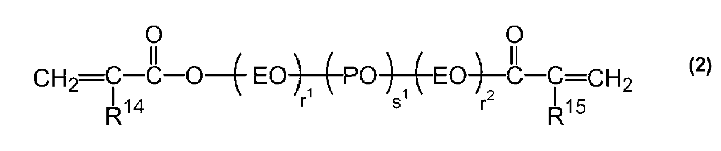
式(2)中、R14及びR15はそれぞれ独立に水素原子又はメチル基を示し、EO及びPOは上記と同義であり、s1は1~30を示し、r1及びr2はそれぞれ0~30を示し、r1+r2は1~30である。式(2)で表される化合物の市販品の例としては、R14及びR15がメチル基、r1+r2=4(平均値)、s1=12(平均値)であるビニル化合物(昭和電工マテリアルズ株式会社製、商品名:FA-023M)が挙げられる。
光重合開始剤の具体例としては、ベンゾフェノン、N,N’-テトラメチル-4,4’-ジアミノベンゾフェノン(ミヒラーケトン)、N,N’-テトラエチル-4,4’-ジアミノベンゾフェノン、4-メトキシ-4’-ジメチルアミノベンゾフェノン、2-ベンジル-2-ジメチルアミノ-1-(4-モルホリノフェニル)-ブタノン-1、2-メチル-1-[4-(メチルチオ)フェニル]-2-モルフォリノ-プロパノン-1等の芳香族ケトン;2-エチルアントラキノン、フェナントレンキノン、2-tert-ブチルアントラキノン、オクタメチルアントラキノン、1,2-ベンズアントラキノン、2,3-ベンズアントラキノン、2-フェニルアントラキノン、2,3-ジフェニルアントラキノン、1-クロロアントラキノン、2-メチルアントラキノン、1,4-ナフトキノン、9,10-フェナンタラキノン、2-メチル1,4-ナフトキノン、2,3-ジメチルアントラキノン等のキノン類;ベンゾインメチルエーテル、ベンゾインエチルエーテル、ベンゾインフェニルエーテル等のベンゾインエーテル化合物、ベンゾイン、メチルベンゾイン、エチルベンゾイン等のベンゾイン化合物;ベンジルジメチルケタール等のベンジル誘導体、2-(o-クロロフェニル)-4,5-ジフェニルイミダゾール二量体、2-(o-クロロフェニル)-4,5-ジ(メトキシフェニル)イミダゾール二量体、2-(o-フルオロフェニル)-4,5-ジフェニルイミダゾール二量体、2-(o-メトキシフェニル)-4,5-ジフェニルイミダゾール二量体、2-(p-メトキシフェニル)-4,5-ジフェニルイミダゾール二量体等の2,4,5-トリアリールイミダゾール二量体;9-フェニルアクリジン、1,7-ビス(9,9’-アクリジニル)ヘプタン等のアクリジン誘導体、N-フェニルグリシン、N-フェニルグリシン誘導体、クマリン系化合物が挙げられる。これらは、単独で又は2種類以上を組み合わせて使用される。光重合開始剤が、2,4,5-トリアリールイミダゾール二量体、特に2-(O-クロロフェニル)-4,5-ジフェニルイミダゾール二量体を含んでもよい。
感光性樹脂組成物におけるバインダーポリマーの含有量は、バインダーポリマー及び光重合性化合物の合計量100質量部に対して、40~80質量部、45~75質量部、又は50~70質量部であってもよい。感光性樹脂組成物における光重合開始剤の含有量は、バインダーポリマー及び光重合性化合物の合計量100質量部に対して、0.01~5質量部、0.1~4.5質量部、又は1~4質量部であってもよい。
感光性樹脂組成物には、必要に応じてその他の成分を含んでもよい。その他の成分の例としては、カチオン重合可能な環状エーテル基を有する光重合性化合物、カチオン重合開始剤、増感剤、マラカイトグリーン等の染料、トリブロモメチルフェニルスルホン、ロイコクリスタルバイオレット等の光発色剤、熱発色防止剤、p-トルエンスルホンアミド等の可塑剤、顔料、充填剤、消泡剤、難燃剤、安定剤、密着性付与剤、レベリング剤、剥離促進剤、酸化防止剤、香料、イメージング剤、及び熱架橋剤が挙げられる。その他の成分の含有量は、バインダーポリマー及び光重合性化合物の合計量100質量部に対して、それぞれ0.01~20質量部程度であってもよい。
感光性樹脂組成物におけるバインダーポリマー、光重合性化合物及び光重合開始剤の合計の含有量は、感光性樹脂組成物のうち溶剤以外の成分の合計質量に対して、90~100質量%、又は95~100質量%であってもよい。
レジスト層30を形成するために、感光性樹脂組成物を含むレジストフィルムを金属層20上に積層してもよいし、溶剤を含む感光性樹脂組成物を金属層20に塗布し、塗膜から溶剤を除去してもよい。
このようなレジスト層30を形成するレジスト材料(ドライレジスト)は、剥離液によって剥離する際に膨潤することがある。例えば、このようなレジスト材料は、10倍に希釈した剥離液に22℃で1分間浸漬した後の膨潤率が30重量%以下であってもよい。また、このレジスト材料は、10倍に希釈した剥離液に22℃で1分間浸漬した後の膨潤率が5重量%以上であってもよく、10重量%以上20重量%以下であってもよい。なお、剥離液は、汎用の剥離液とすることができる。
このようなレジスト材料の膨潤率は、QCM(Quartz Crystal Microbalance)法を用いて測定することができる。具体的には、例えば、固有振動数5MHzのQCM(IPN 603800 Rww.K、INFICON社製)を用いて測定することができる。まず、QCMの上に感光性フィルムであるレジスト材料を実際の配線形成工程と同様の条件でラミネートする。その後、実際の配線形成工程と同様の条件で光照射を行う。光照射後の上記サンプルのレジスト材料(膜厚25μm)をQCMセンサーにセットし、下記の剥離液の入ったビーカーに浸漬させる。
剥離液:一般的な汎用剥離液(例えば、R-100S 15vol%+R-101 8vol%(三菱ガス化学製)を10倍に希釈した溶液
測定温度:22℃
レジスト膨潤に応じてQCMクリスタルの振動数が低くなるため、測定データとしては含浸時間に対する振動数変化Δfが得られる。そして、下記のSauebreyの式(1)に基づいて、重量変化(Δm)を算出する。
Δf=Cf×Δm・・・(1)
Cfは使用するクリスタルの感度因子(sensitivity factor of crystal)であり、単位は(Hz/ng/cm2)である。5MHzのクリスタルを用いた場合、Cf=0.056である。本実施形態では、測定開始から1分後の重量変化率Δm/m(初期のレジスト重量)を膨潤率(%)としている。なお、例えば、ドライレジストA(商品名:RD1225、昭和電工マテリアルズ株式会社製)の上記膨潤率は20%であり、ドライレジストB(商品名:RY5125、昭和電工マテリアルズ株式会社製)の上記膨潤率は15%である。上記の膨潤率を10%程度にしたドライレジストも適宜提供可能である。
剥離液:一般的な汎用剥離液(例えば、R-100S 15vol%+R-101 8vol%(三菱ガス化学製)を10倍に希釈した溶液
測定温度:22℃
レジスト膨潤に応じてQCMクリスタルの振動数が低くなるため、測定データとしては含浸時間に対する振動数変化Δfが得られる。そして、下記のSauebreyの式(1)に基づいて、重量変化(Δm)を算出する。
Δf=Cf×Δm・・・(1)
Cfは使用するクリスタルの感度因子(sensitivity factor of crystal)であり、単位は(Hz/ng/cm2)である。5MHzのクリスタルを用いた場合、Cf=0.056である。本実施形態では、測定開始から1分後の重量変化率Δm/m(初期のレジスト重量)を膨潤率(%)としている。なお、例えば、ドライレジストA(商品名:RD1225、昭和電工マテリアルズ株式会社製)の上記膨潤率は20%であり、ドライレジストB(商品名:RY5125、昭和電工マテリアルズ株式会社製)の上記膨潤率は15%である。上記の膨潤率を10%程度にしたドライレジストも適宜提供可能である。
[工程C]
工程Cでは、レジスト層30の形成が終了すると、レジスト層30を露光する。工程Cでは、例えば、図2に示す構成の露光パターン40となるように、レチクル(フォトマスクとも言う)をレジスト層30の上方に配置して所定の露光を行う。このような露光により、レジスト層30は、図2に示すように、配線電極2(金属配線)に対応する配線用露光パターン41(配線用露光パターン)と、配線電極に対応しないダミー露光パターン42とに露光される。なお、図1の(b)には、配線用露光パターン41によって露光されるレジスト部分31と、ダミー露光パターン42によって露光されるレジスト部分32とを示している。
工程Cでは、レジスト層30の形成が終了すると、レジスト層30を露光する。工程Cでは、例えば、図2に示す構成の露光パターン40となるように、レチクル(フォトマスクとも言う)をレジスト層30の上方に配置して所定の露光を行う。このような露光により、レジスト層30は、図2に示すように、配線電極2(金属配線)に対応する配線用露光パターン41(配線用露光パターン)と、配線電極に対応しないダミー露光パターン42とに露光される。なお、図1の(b)には、配線用露光パターン41によって露光されるレジスト部分31と、ダミー露光パターン42によって露光されるレジスト部分32とを示している。
配線用露光パターン41は、多数の配線電極2のそれぞれに対応する遮蔽部41aを多数有する部分である。遮蔽部41aは、所定波長の光で露光された場合に照射された光を遮蔽して、レジスト層30において対応する領域の露光をさせないための領域である。レジスト層30の一部をこのように露光することで、反応が一部進行したレジスト層30が形成される。露光は、当業者に知られる通常の方法によって行うことができる。レジスト層30がネガ型レジストから形成される場合、露光された箇所が現像液に対して溶解性が低下し、現像によって露光した領域が残ることになる。即ち、露光が遮蔽部41aによって遮蔽された領域が、現像液によって溶解されることになる。
ダミー露光パターン42は、配線用露光パターン41の全体を取り囲むように形成される露光パターンであり、複数の線を格子状に配置したメッシュ形状を含んで形成されている。このようなメッシュ形状のダミー露光パターン42を配線用露光パターン41の外側に設けることにより、配線用露光パターン41の外側のレジスト層30を細かい部分に分けることができる。これにより、後述するレジストの剥離工程における剥離片を小さくすることができ、また、レジストの剥離を早めることが可能となる。なお、ダミー露光パターン42は、図2に示す構成に限定されず、後述するように、各種の形態を採用し得る。
ダミー露光パターン42は、より詳細には、図3に示すように、配線用露光パターン41の外周側の端部41bに近接して配置されており、配線用露光パターン41の外周側の端部41bとダミー露光パターン42(再内周部分)との間の距離Dが200μm以内となるように形成されている。言い換えると、ダミー露光パターン42の少なくとも一部は、配線用露光パターン41の端部41bから200μm以内の領域に位置する。この配線用露光パターン41とダミー露光パターン42との間の距離Dは、例えば150μm以下であってもよく、100μm以下であってもよく、50μm以下であってもよい。一例として、距離Dは、70~80μmである。
ダミー露光パターン42のメッシュを形成する線状の部分42a,42a同士の離隔距離A(双方の中心線の間の距離)は、例えば、1μm以上100μm以下であってもよく、1μm以上75μm以下であってもよく、1μm以上50μm以下であってもよい。一例として、離隔距離Aは、50μmである。また、各線状の部分42aの線幅Wは、1μm以上20μm以下であってもよく、1μm以上10μm以下であってもよく、1μm以上5μm以下であってもよい。一例として、線幅Wは5μmである。
本実施形態における露光は、上述したように、フォトマスクであるレチクルを用いた露光であってもよいが、配線用露光パターン41に対応する配線用露光データと、ダミー露光パターン42に対応するダミー露光データとを備えた露光データ(露光描画データ構造)に基づいて、露光装置のレーザ又は電子銃等のビームにより露光パターンをレジスト層30に描画するようにしてもよい。
[工程D]
工程Dでは、図1の(c)に示すように、露光されたレジスト層30を現像してレジスト層30に複数の開口35,35aを形成する。開口35は、配線基板1における配線電極2に対応する部分であり、開口35aは、配線基板1におけるダミー金属構造物2aに対応する部分である。現像工程では、工程Cでの露光後、所定時間(例えば30分)、レジスト層30を放置し、レジストフィルムの保護フィルムをはく離し、例えば、1.0%炭酸ナトリウム水溶液等の現像液を用いて現像処理を行う。これにより、露光されていない部分が溶解して、開口35,35aが形成される。開口35,35aが形成される場合、めっき処理の際のシード層となる金属層20が開口35,35a内に露出する。開口35,35aは、例えば、短手方向の幅が5μm程度の凹部であり、紙面に直交する方向に延在する。開口35及び開口35aは、同じ大きさであってもよいし、開口35aの幅又は径が開口35より大きくてもよく、開口35aの幅又は径が開口35より小さくてもよい。
工程Dでは、図1の(c)に示すように、露光されたレジスト層30を現像してレジスト層30に複数の開口35,35aを形成する。開口35は、配線基板1における配線電極2に対応する部分であり、開口35aは、配線基板1におけるダミー金属構造物2aに対応する部分である。現像工程では、工程Cでの露光後、所定時間(例えば30分)、レジスト層30を放置し、レジストフィルムの保護フィルムをはく離し、例えば、1.0%炭酸ナトリウム水溶液等の現像液を用いて現像処理を行う。これにより、露光されていない部分が溶解して、開口35,35aが形成される。開口35,35aが形成される場合、めっき処理の際のシード層となる金属層20が開口35,35a内に露出する。開口35,35aは、例えば、短手方向の幅が5μm程度の凹部であり、紙面に直交する方向に延在する。開口35及び開口35aは、同じ大きさであってもよいし、開口35aの幅又は径が開口35より大きくてもよく、開口35aの幅又は径が開口35より小さくてもよい。
露光後のレジスト層30を上述したように現像することにより、金属層20が露出した開口35,35aを含むレジスト層30が形成される。現像は、当業者に知られる通常の方法によって行うことができる。現像のための現像液は、炭酸ナトリウム水溶液のようなアルカリ水溶液であってもよい。
なお、後述するように、ダミー露光パターン42の線幅がレジストの解像度以下の場合、現像によって形成される開口35aが完全ではなく、金属層20が開口35a内に露出しない。この場合、後の工程で35aに該当する箇所にダミー金属構造物2aが形成されないものの、剥離工程時に未露光であるダミー露光パターン42の線状部分から溶液が浸透し、ダミー部分を境としてレジスト層30が小片化しやすい状態となる。つまり、開口35aに対応する部分が、次の剥離工程の際に小片化されやすい状態のレジスト部分となる。これにより、剥離時にレジストが個片化し配線にかかる応力が小さくなり、ダミー金属構造物が形成されなくとも歩留まりを向上させることができる。加えて、ダミーパターンを有することで溶液の浸透が速くなるため、剥離工程時間の短縮にもつながる。
[工程E]
工程Eでは、図1の(d)に示すように、複数の開口35,35a内に露出した金属層20をシード層として電解めっきによって金属層21,21aを形成して、複数の開口35,35a内に配線電極2及びダミー金属構造物2aを形成する。この工程では、例えば、銅めっきにより開口35,35aが充填される。金属層21の形成方法は、電解めっき、無電解めっき、金属含有ペーストの注入および焼結、およびこれらの組み合わせであってもよい。
工程Eでは、図1の(d)に示すように、複数の開口35,35a内に露出した金属層20をシード層として電解めっきによって金属層21,21aを形成して、複数の開口35,35a内に配線電極2及びダミー金属構造物2aを形成する。この工程では、例えば、銅めっきにより開口35,35aが充填される。金属層21の形成方法は、電解めっき、無電解めっき、金属含有ペーストの注入および焼結、およびこれらの組み合わせであってもよい。
金属層21を形成する金属は、例えば、銅、金、銀、ニッケル、スズ、チタン、タングステン、モリブデン、コバルト、クロム、鉄、及び亜鉛からなる群より選ばれる少なくとも1種の金属を含んでいてもよい。金属層21,21aは単層であってもよいし、2層以上から構成されていてもよい。金属層21,21aの厚さは、例えば0.1~10.0μmであってもよく、1~150μmであってもよい。
金属層21,21aは、線状部を含んでいてもよく、その幅が1~20μmであってもよい。言い換えると、金属層21,21aを含んで構成される配線電極2及びダミー金属構造物2aのライン/スペース(L/S)は、1μm/1μm~20μm/20μmであってもよい。本実施形態に係る方法によれば、ダミー露光パターン42を含んで露光パターンで露光しているため、このような微細な配線であっても、配線の剥離及び倒れのような欠陥が生じる可能性が小さい。
金属層21,21aは、円状部を含んでいてもよく、直径が5~100μmであってもよく、直径が20μm以下であってもよい。本実施形態に係る方法によれば、ダミー露光パターン42を含んで露光パターンで露光しているため、このような微細な配線であっても、配線の剥離及び倒れのような欠陥が生じる可能性が小さい。なお、上述したように、ダミー露光パターン42の線幅がレジストの解像度以下であり、開口35aが完全に形成されない場合、金属層21a及びダミー金属構造物2aも形成されない。
[工程F]
工程Fでは、開口35,35aへの金属層21,21aの形成が終了すると、図1の(e)に示すように、レジスト層30を金属層20から剥離する。このような剥離は、一般的に用いられている剥離液を用いて行う。汎用的な剥離液の例については、上述した通りである。
工程Fでは、開口35,35aへの金属層21,21aの形成が終了すると、図1の(e)に示すように、レジスト層30を金属層20から剥離する。このような剥離は、一般的に用いられている剥離液を用いて行う。汎用的な剥離液の例については、上述した通りである。
[工程G]
工程Gでは、図1の(f)に示すように、レジスト層30の剥離により露出した部分の金属層20、即ち、金属層21,21aに結合している領域を除いた部分を、エッチング等の方法によって除去する。これにより、支持体10上に残った金属層20と金属層21とから構成される配線電極2が形成され、金属層20と金属層21aとから構成されるダミー金属構造物2aが形成される。なお、ダミー金属構造物2aは、配線電極2のレジストによる倒れを防止するための部材であるため、電気的には他の電極(例えば配線電極2又は支持体10中の電極等)に対して絶縁されていることが好ましい。
工程Gでは、図1の(f)に示すように、レジスト層30の剥離により露出した部分の金属層20、即ち、金属層21,21aに結合している領域を除いた部分を、エッチング等の方法によって除去する。これにより、支持体10上に残った金属層20と金属層21とから構成される配線電極2が形成され、金属層20と金属層21aとから構成されるダミー金属構造物2aが形成される。なお、ダミー金属構造物2aは、配線電極2のレジストによる倒れを防止するための部材であるため、電気的には他の電極(例えば配線電極2又は支持体10中の電極等)に対して絶縁されていることが好ましい。
以上の工程により、図1の(f)に示すように、支持体10と、支持体10上に設けられた複数の配線電極2と、複数のダミー金属構造物2aとを備えた配線基板1を得ることができる。ダミー金属構造物2aは、ダミー露光パターン42と同様に、複数の配線電極2を取り囲むように形成され、ダミー金属構造物2aの少なくとも一部は、複数の配線電極2のうちダミー金属構造物2aに最も近い配線電極から200μm以内の領域に位置する。また、配線基板1は、ダミー露光パターン42に基づいて作製されるダミー金属構造物2aが形成されない構成であってもよい。以下、説明する。
図4及び図5を参照して、工程Cの露光工程~工程Eの電極形成工程について、更に詳細に説明する。図4は、ダミー露光パターンに対応する領域の露光及び現像の例を示す断面図であり、ダミー露光パターンの幅がレジストの解像度以上の場合の例を示す。図4の方法は、上述した方法と同様である。図5は、ダミー露光パターンに対応する領域の露光及び現像の例を示す断面図であり、ダミー露光パターンの幅がレジストの解像度よりも小さい場合の例を示す。なお、以下では、ダミー露光パターン42による露光部分での製造方法について主に説明し、配線用露光パターン41による露光部分での製造方法は上述したものと同様であり、説明を省略する。
ダミー露光パターン42の幅がレジスト層30を形成するレジストの解像度以上の場合、工程A及び工程Bに続いて、まずは図4の(a)に示すように、幅広のダミー露光パターン42を用いて、レジスト層30を露光する(工程C)。その後、図4の(b)及び(c)に示すように、工程Dの現像工程、工程Eの電極の形成工程を行い、ダミー金属構造物2a用の金属層21aを形成する。
その後、図4の(d)に示すように、工程Fのレジスト剥離工程にて、ダミー金属構造物2a用の金属層21aの外側にあるレジスト層30を剥離する。この剥離の際、レジスト層30は細かなレジスト片30aとなって剥離される。この場合、ダミー金属構造物2aに近接する配線電極2は、レジスト層30のレジストが膨張することによる応力からダミー金属構造物2aによって保護され、傾いたり又は倒されたりすることが抑制される。また、レジスト層30自体が小片となるため、レジストの膨張による応力が低下され、この点でも、配線電極2は傾いたり又は倒されたりすることが抑制される。
一方、ダミー露光パターン42の幅がレジスト層30を形成するレジストの解像度より小さい場合、工程A及び工程Bに続いて、まずは図5の(a)に示すように、幅狭のダミー露光パターン42を用いて、レジスト層30を露光する(工程C)。その後、図5の(b)に示すように、工程Dの現像工程を行う。この際、ダミー露光パターン42の幅がレジストの解像度よりも小さいため、現像液による現像によって形成される開口35aが完全ではなく、金属層20が開口35a内に露出しない。また、金属層20が露出しないため、図5の(c)に示すように、工程Eでの電極形成工程においてダミー金属構造物が形成されない。
その後、図5の(d)に示すように、工程Fのレジスト剥離工程にて、レジスト層30を剥離する。この剥離の際、レジスト層30は細かなレジスト片30aとなって剥離される。この場合、ダミー露光パターン42によって形成されるダミー領域42aに近接する配線電極2は、レジスト層30が小片となるため、レジストの膨張による応力が低下され、ダミー金属構造物2aを設けなくても配線電極2が傾いたり又は倒されたりすることが抑制される。ダミー領域42aにおいて金属層20が露出していなくても、露光部分に比べてダミー領域42aは硬化が弱いため、剥離液が該当部に浸透しやすく、レジストが小片化しながら剥離するため上述した剥離時の応力緩和効果を十分に得ることができる。また、ダミー領域42aにおいて金属層20が露出しない場合、ダミー領域42aにめっきが析出することがなく、配線基板に必要となる配線部のみにめっきを析出して配線電極2を形成することが可能となる。つまり、この場合、図1の(f)に示すダミー金属構造物2aを有しない配線基板を得ることできる。
以上、本実施形態に係る配線基板の製造方法では、配線基板1における配線等を構成する配線電極2に対応する配線用露光パターン41の端部41bから200μm以内の領域に、配線電極2を構成するものではないダミー露光パターン42の少なくとも一部が位置する。この場合、ダミー露光パターン42によって露光された領域にダミー金属構造物2aを設けたり、又は、ダミー露光パターン42を設けることでその領域におけるレジスト層30を小片化したりすることにより、配線電極2へのレジストからの応力を低下させることができる。これにより、配線基板1の製造工程中にレジストの応力によって配線電極2が倒れてしまうことを、隣接するダミー露光パターン42(又はダミー金属構造物2a)によって防止することができる。よって、この配線基板の製造方法によれば、歩留まりの低下を抑制することができる。
また、本実施形態に係る配線基板の製造方法では、レジスト層30を形成する工程において、支持体10上に設けられた金属層20上にレジスト層30を形成し、開口を形成する工程では、金属層20が開口35から露出し、配線を形成する工程では、開口35内に露出した金属層20上に電解めっきを析出させて配線電極2を形成している。この場合、SAP法又はMSAP法等により金属配線を形成して、より微細な配線電極2を容易に形成することができる。よって、この配線基板の製造方法によれば、金属配線の微細化、又は、小径化等を実現することが可能となる。
また、本実施形態に係る配線基板の製造方法では、ダミー露光パターン42は、配線用露光パターンの全体若しくは一部を取り囲んでいる。配線電極2の外側部分がレジスト剥離によって倒れやすい傾向にあるが、ダミー露光パターン42をこのような配置にすることにより、配線電極2の倒れをより確実に抑制して、歩留まりの低下を抑制することができる。
また、本実施形態に係る配線基板の製造方法では、ダミー露光パターン42は、複数の線を格子状に配置したメッシュ形状を含んでいる。この場合、配線電極等のレジスト剥離による倒れをダミー露光パターンでより確実に抑制して、歩留まりの低下を抑制することができる。
また、本実施形態に係る配線基板の製造方法では、配線電極2の短手方向の幅または直径が20μm以下であってもよい。この場合、配線電極2等をより微細又は微小にすることができ、微細又は微小な配線電極を設けた場合であっても、配線電極の倒れを抑制して歩留まりの低下を抑制することができる。
また、本実施形態に係る配線基板の製造方法では、レジスト層30を露光する工程では、配線用露光パターン41とダミー露光パターン42とを含むレチクルを用いて、レジスト層30を露光している。この場合、各露光工程の時間を低減できるため、配線基板1の製造効率を向上することができる。また、各露光工程間でのズレを低減することができるため、配線基板1の製造歩留まりを向上することができる。
また、本実施形態に係る配線基板の製造方法では、レジスト層30を露光する工程では、配線用露光パターン41とダミー露光パターン42とを含む露光描画データに基づいて描画を行い、レジスト層30を露光してもよい。この場合、レチクル等の部材が不要となるため、その分の製造コストを低減することができる。また、露光描画データを作成又は修正することで、露光パターンの作成又は修正を容易に行うことができる。
また、本実施形態に係る配線基板の製造方法では、ダミー露光パターン42は、線状の部分を有し、線状の部分の幅がレジスト層30を構成するレジストの解像度以下であってもよい。この場合、ダミー露光パターン42に基づいてダミー金属構造物が形成されないものの、露光されたレジスト層30が分割されて小片化しやくなるため、レジスト剥離の際に配線電極2を倒してしまうといったことを抑制できる。これにより、この製造方法によれば、歩留まりの低下を抑制することができる。また、この製造方法では、ダミー露光パターン42に基づいてダミー金属構造物が形成されづらいため、作製された配線基板1では不要となる部分を残した構成としなくてよくなる。
以上、本開示の実施形態について説明したが、本発明は上述した実施形態に限定されるものではなく、その趣旨を逸脱しない範囲で適宜変更を行ってもよい。例えば、露光パターン40は、図6及び図7に示す構成の露光パターンであってもよい。図6の(a)に示すように、露光パターンとして、線状の配線電極2に対応する配線用露光パターン41Aの一部(図の例では三方向)を取り囲むダミー露光パターン42Aを有する露光パターン40Aを用いてもよい。このダミー露光パターン42Aは、メッシュ形状であってもよい。この場合も、配線電極2に対応する配線用露光パターン41Aの端部から200μm以内の領域に、ダミー露光パターン42Aの少なくとも一部が位置しており、配線電極2の倒れを抑制する。以下の変形例でも同様である。
また、図6の(b)に示すように、露光パターンとして、線状の配線電極2に対応する配線用露光パターン41Aの一部(図の例では三方向)を取り囲むダミー露光パターン42Bを有する露光パターン40Bを用いてもよい。このダミー露光パターン42Bは、ドット形状の遮光部を多数設けて、配線用露光パターン41Aの一部を覆うように形成されている。ドット形状の遮光部は、平面視で、丸、三角、四角、バツ印などの幾何学的なパターン及びそれらの組み合わせを呈してもよい。このように、ダミー露光パターンとしては各種のパターンを用いることができ、レジスト層30のレジストの剥離を早めたり、剥離片を小さくすることができる構成であれば、各種のパターンを採用することができる。なお、ここでいう配線電極2は、上記同様に、例えば、チップ若しくは基板における水平方向の電気的接続のために形成される配線電極である。
また、図7の(a)に示すように、円形の端子電極3(金属配線)に対応する端子用露光パターン41C(配線用露光パターン)の全体を取り囲むように、ダミー露光パターン42Cを設けた露光パターン40Cであってもよい。ダミー露光パターン42Cでは、端子用露光パターン41Cを二重に取り囲むように構成されている。また、図7の(b)に示すように、露光パターンとして、ダミー露光パターン42Cの構成に加えて、更に、複数の端子電極3の間に内側ダミー露光パターン42D(内側ダミー金属構造物に対応)が位置する構成の露光パターン40Dを用いてもよい。この場合、端子電極3間のピッチが広くなっていてもよい。また、図7の(c)に示すように、露光パターンとして、端子電極3に対応する端子用露光パターン41Cの全体を一重で(線状に)取り囲むように、ダミー露光パターン42Eを設けた露光パターン40Eを用いてもよい。なお、ここでいう端子電極3は、例えば、垂直方向の電気的接続のために形成される端子電極である。端子電極3は、例えば、垂直方向の電気的接続のために形成される突起電極であってもよい。
以下、実施例を挙げて本発明についてさらに具体的に説明する。ただし、本発明はこれら実施例に限定されるものではない。
[マスクの用意]
実施例1として、Cr遮蔽部を有するレチクル40Fを用意した(図8を参照)。レチクルのデザインパターンとしては、ライン/スペース(L/S)=5μm/5μmの線状の配線構造を有するものであった(配線用露光パターン41F)。加えて、上記微細配線の外側にライン幅30μmのダミー配線を有するデザインとした(ダミー露光パターン42F)。ダミー露光パターン42Fと配線用露光パターン41Fとの最も近い距離D(図3を参照)は、20μmであった。
実施例1として、Cr遮蔽部を有するレチクル40Fを用意した(図8を参照)。レチクルのデザインパターンとしては、ライン/スペース(L/S)=5μm/5μmの線状の配線構造を有するものであった(配線用露光パターン41F)。加えて、上記微細配線の外側にライン幅30μmのダミー配線を有するデザインとした(ダミー露光パターン42F)。ダミー露光パターン42Fと配線用露光パターン41Fとの最も近い距離D(図3を参照)は、20μmであった。
[配線層の形成]
[レジスト層の形成]
150mm角、厚み0.81mmのプリント配線板用の銅張積層板(昭和電工マテリアルズ株式会社)上に、ラミネーター(ラミーコーポレーション社製、GK-13DX)を用いて、ネガ型のレジストフィルム(昭和電工マテリアルズ社製、厚み25μm)をラミネートした。ラミネート温度は110℃、ラミネート速度は1.4m/分、ラミネート圧力は0.5MPaとした。ラミネート後、30分放置し、レジストフィルムをi線ステッパー(サーマプレシジョン社製、S6Ck)、及びネガ型フォトマスクを用いて露光した。照度は33mW/cm2、露光量は120mJ/cm2とした。ネガ型フォトマスクは上述したものを用いた。また、使用したレジストフィルムは、10倍に希釈した剥離液(後述)に22℃で1分間浸漬した後の膨潤率が15重量%以下のものを用いた。
[レジスト層の形成]
150mm角、厚み0.81mmのプリント配線板用の銅張積層板(昭和電工マテリアルズ株式会社)上に、ラミネーター(ラミーコーポレーション社製、GK-13DX)を用いて、ネガ型のレジストフィルム(昭和電工マテリアルズ社製、厚み25μm)をラミネートした。ラミネート温度は110℃、ラミネート速度は1.4m/分、ラミネート圧力は0.5MPaとした。ラミネート後、30分放置し、レジストフィルムをi線ステッパー(サーマプレシジョン社製、S6Ck)、及びネガ型フォトマスクを用いて露光した。照度は33mW/cm2、露光量は120mJ/cm2とした。ネガ型フォトマスクは上述したものを用いた。また、使用したレジストフィルムは、10倍に希釈した剥離液(後述)に22℃で1分間浸漬した後の膨潤率が15重量%以下のものを用いた。
露光後、60分放置し、レジストフィルムの保護フィルムをはく離し、1.0%炭酸ナトリウム水溶液を用いた現像により、シード層が露出するライン/スペース(L/S)=5μm/5μmの線状パターンおよび上記微細配線の外側にライン幅30μmのダミー線状パターンを有するレジスト層を形成した。現像は、超高圧スピン現像装置(ブルーオーシャンテクノロジー社製)を用いて、現像液を260秒間スプレーし、次いでリンス液として純水を100秒間スプレーすることによって行った。現像温度は30℃、回転数は500rpm、スプレー圧は0.18MPa、スプレーノズルヘッドの移動距離は7.2cm、スプレーノズルヘッドの移動速度は10cm/sであった。
[クリーナー前処理]
シード層及びレジスト層が形成された基板を、酸性クリーナー(JCU社製、PB-242D)の100mL/L水溶液に45℃で5分間浸漬した。その後、シード層及びレジスト層が形成された基板を、50℃の純水に1分間、25℃の純水に1分間、25℃の10%硫酸水溶液に1分間の順に浸漬した。
シード層及びレジスト層が形成された基板を、酸性クリーナー(JCU社製、PB-242D)の100mL/L水溶液に45℃で5分間浸漬した。その後、シード層及びレジスト層が形成された基板を、50℃の純水に1分間、25℃の純水に1分間、25℃の10%硫酸水溶液に1分間の順に浸漬した。
[Cu電解めっき]
その後、酸洗浄処理後のレジスト層付き銅張積層板を電解銅めっき液に浸漬し、25℃で10分間電解銅めっきをおこなった。電解銅めっき液として、硫酸銅5水和物の120g/L、96%硫酸220g/Lの水溶液7.3L、塩酸0.26mL、トップルチナNSV-1(商品名、奥野製薬工業製)92mL、トップルチナNSV-2(商品名、奥野製薬工業製)11.5mL、及びトップルチナNSV-3(商品名、奥野製薬工業製)23mLの混合液を用いた。
その後、酸洗浄処理後のレジスト層付き銅張積層板を電解銅めっき液に浸漬し、25℃で10分間電解銅めっきをおこなった。電解銅めっき液として、硫酸銅5水和物の120g/L、96%硫酸220g/Lの水溶液7.3L、塩酸0.26mL、トップルチナNSV-1(商品名、奥野製薬工業製)92mL、トップルチナNSV-2(商品名、奥野製薬工業製)11.5mL、及びトップルチナNSV-3(商品名、奥野製薬工業製)23mLの混合液を用いた。
[レジスト剥離]
電解めっき処理後の基板上に存在するレジスト層を剥離することにより、銅配線を有する基板を形成した。剥離は、フォトリソ用現像装置AD-3000(滝沢産業株式会社製)を用いて、剥離液を300秒間スプレーし、次いでリンス液として純水を30秒間スプレーすることによって行った。剥離温度は50℃、回転数は500rpm、スプレー圧は0.18MPa、スプレーノズルヘッドの移動距離は7.2cm、スプレーノズルヘッドの移動速度は10cm/sであった。剥離液として、A-06A(商品名、花王製)150mL/L、A-06B(商品名、花王製)80mL/Lの混合液を用いた。
電解めっき処理後の基板上に存在するレジスト層を剥離することにより、銅配線を有する基板を形成した。剥離は、フォトリソ用現像装置AD-3000(滝沢産業株式会社製)を用いて、剥離液を300秒間スプレーし、次いでリンス液として純水を30秒間スプレーすることによって行った。剥離温度は50℃、回転数は500rpm、スプレー圧は0.18MPa、スプレーノズルヘッドの移動距離は7.2cm、スプレーノズルヘッドの移動速度は10cm/sであった。剥離液として、A-06A(商品名、花王製)150mL/L、A-06B(商品名、花王製)80mL/Lの混合液を用いた。
(比較例1)
[マスクの用意]
比較例1では、Cr遮蔽部を有するレチクル140Aを用意した。デザインとしては、図9に示すように、ライン/スペース(L/S)=5μm/5μmの線状の配線構造を有するものであった(配線用露光パターン141F)。図9に示すレチクル140Aでは、ダミーパターンは形成されていなかった。
2.配線層の形成
[マスクの用意]
比較例1では、Cr遮蔽部を有するレチクル140Aを用意した。デザインとしては、図9に示すように、ライン/スペース(L/S)=5μm/5μmの線状の配線構造を有するものであった(配線用露光パターン141F)。図9に示すレチクル140Aでは、ダミーパターンは形成されていなかった。
2.配線層の形成
用いたレチクルのデザインが異なる以外は、実施例1と同様の条件で、レジスト層の形成、クリーナー前処理、Cu電解めっきの形成、レジスト剥離を行った。
[倒れの観察の評価]
形成された銅配線を、光学顕微鏡を用いて観察した。倒れが観察された配線の数およびデザインされた配線本数に対する倒れた配線の割合を表1にまとめた。また、図10に、比較例1による配線電極の写真を示す。
形成された銅配線を、光学顕微鏡を用いて観察した。倒れが観察された配線の数およびデザインされた配線本数に対する倒れた配線の割合を表1にまとめた。また、図10に、比較例1による配線電極の写真を示す。

以上、表1に示されるように、露光デザインパターンにおいて、配線用露光パターンに隣接してダミー露光パターンを含めることで、高アスペクトのめっきパターンの倒れを抑制でき、歩留まりを向上できることが確認された。
1…配線基板、2…配線電極、2a…ダミー金属構造物、3…端子電極、10…支持体、20…金属層、30…レジスト層、35,35a…開口、40,40A,40B,40C,40D,40E…露光パターン、40F…レチクル、41,41A……配線用露光パターン、41C…端子用露光パターン、41b…端部、42,42A,42B,42C,42D,42E…ダミー露光パターン。
Claims (15)
- 支持体上にレジスト層を形成する工程と、
前記レジスト層を露光する工程と、
前記露光された前記レジスト層を現像して前記レジスト層に開口を形成する工程と、
前記開口内に金属配線を形成する工程と、
前記金属配線が形成された後に前記レジスト層を除去する工程と、を備え、
前記レジスト層を露光する工程では、前記金属配線に対応する配線用露光パターンと前記金属配線に対応しないダミー露光パターンとを前記レジスト層に露光し、
前記ダミー露光パターンの少なくとも一部は、前記配線用露光パターンの端部から200μm以内の領域に位置する、配線基板の製造方法。 - 前記レジスト層を形成する工程では、前記支持体上に設けられた金属層上に前記レジスト層を形成し、
前記開口を形成する工程では、前記金属層が前記開口から露出し、
前記金属配線を形成する工程では、前記開口内に露出した前記金属層上に電解めっきを析出させて前記金属配線を形成する、
請求項1に記載の配線基板の製造方法。 - 前記ダミー露光パターンは、前記配線用露光パターンの少なくとも一部を取り囲む、
請求項1又は2に記載の配線基板の製造方法。 - 前記ダミー露光パターンは、前記配線用露光パターンの全体を取り囲む、
請求項3に記載の配線基板の製造方法。 - 前記ダミー露光パターンは、複数の線を格子状に配置したメッシュ形状を含む、
請求項1~4の何れか一項に記載の配線基板の製造方法。 - 前記金属配線の短手方向の幅が20μm以下である、
請求項1~5の何れか一項に記載の配線基板の製造方法。 - 前記レジスト層は、ネガ型のレジストから形成され、
前記レジストは、10倍に希釈した剥離液に22℃で1分間浸漬した後の膨潤率が30重量%以下である、
請求項1~6の何れか一項に記載の配線基板の製造方法。 - 前記ダミー露光パターンは、線状の部分を有し、
前記線状の部分の幅が前記レジスト層を構成するレジストの解像度以下である、
請求項1~7の何れか一項に記載の配線基板の製造方法。 - 前記レジスト層を露光する工程では、前記配線用露光パターンと前記ダミー露光パターンとを含むレチクルを用いて、前記レジスト層を露光する、
請求項1~8の何れか一項に記載の配線基板の製造方法。 - 前記レジスト層を露光する工程では、前記配線用露光パターンと前記ダミー露光パターンとを含む露光描画データに基づいて描画を行い、前記レジスト層を露光する、
請求項1~8の何れか一項に記載の配線基板の製造方法。 - 支持体と、前記支持体上に設けられた複数の金属配線と、前記複数の金属配線の少なくとも一部を取り囲む少なくとも1つのダミー金属構造物と、を備え、
前記金属配線の短手方向の幅は20μm以下であり、
前記ダミー金属構造物の少なくとも一部は、前記複数の金属配線のうち前記ダミー金属構造物に最も近い配線電極から200μm以内の領域に位置する、配線基板。 - 前記ダミー金属構造物は、複数の線を格子状に配置したメッシュ形状のダミー金属構造物、前記複数の金属配線の間に位置する内側ダミー金属構造物、前記複数の金属配線を線状に取り囲むダミー金属構造物、及び、複数のドット状の電極を前記複数の金属配線の少なくとも一部を取り囲むように配置したダミー金属構造物、の少なくとも1つを含む、
請求項11に記載の配線基板。 - レジストを露光するためのレチクルであって、
配線用露光パターンと、前記配線用露光パターンの端部に対して少なくとも一部が200μm以内に位置するダミー露光パターンとを備える、レチクル。 - 前記ダミー露光パターンは、前記配線用露光パターンの少なくとも一部を取り囲むように形成されている、
請求項13に記載のレチクル。 - レジスト層を露光するための露光装置用の露光描画データ構造であって、
前記露光装置に配線用露光パターンを描画させる配線用露光データと、
前記露光装置にダミー露光パターンを描画させるダミー露光データであって、前記ダミー露光パターンの少なくとも一部が前記配線用露光パターンの端部から200μm以内に位置する、ダミー露光データと、
により構成される露光描画データ構造。
Priority Applications (6)
| Application Number | Priority Date | Filing Date | Title |
|---|---|---|---|
| PCT/JP2022/006209 WO2023157136A1 (ja) | 2022-02-16 | 2022-02-16 | 配線基板の製造方法、配線基板、レチクル、及び、露光描画データ構造 |
| CN202380033082.7A CN119156891A (zh) | 2022-02-16 | 2023-02-15 | 配线基板的制造方法、配线基板、光掩模及曝光描绘数据结构 |
| TW112105364A TW202335543A (zh) | 2022-02-16 | 2023-02-15 | 配線基板之製造方法、配線基板、光掩模及曝光描繪資料結構 |
| PCT/JP2023/005191 WO2023157868A1 (ja) | 2022-02-16 | 2023-02-15 | 配線基板の製造方法、配線基板、レチクル、及び、露光描画データ構造 |
| US18/837,891 US20250142731A1 (en) | 2022-02-16 | 2023-02-15 | Wiring substrate production method, wiring substrate, reticle, and exposure pattern-rendering data structure |
| JP2024501400A JPWO2023157868A1 (ja) | 2022-02-16 | 2023-02-15 |
Applications Claiming Priority (1)
| Application Number | Priority Date | Filing Date | Title |
|---|---|---|---|
| PCT/JP2022/006209 WO2023157136A1 (ja) | 2022-02-16 | 2022-02-16 | 配線基板の製造方法、配線基板、レチクル、及び、露光描画データ構造 |
Publications (1)
| Publication Number | Publication Date |
|---|---|
| WO2023157136A1 true WO2023157136A1 (ja) | 2023-08-24 |
Family
ID=87577872
Family Applications (2)
| Application Number | Title | Priority Date | Filing Date |
|---|---|---|---|
| PCT/JP2022/006209 Ceased WO2023157136A1 (ja) | 2022-02-16 | 2022-02-16 | 配線基板の製造方法、配線基板、レチクル、及び、露光描画データ構造 |
| PCT/JP2023/005191 Ceased WO2023157868A1 (ja) | 2022-02-16 | 2023-02-15 | 配線基板の製造方法、配線基板、レチクル、及び、露光描画データ構造 |
Family Applications After (1)
| Application Number | Title | Priority Date | Filing Date |
|---|---|---|---|
| PCT/JP2023/005191 Ceased WO2023157868A1 (ja) | 2022-02-16 | 2023-02-15 | 配線基板の製造方法、配線基板、レチクル、及び、露光描画データ構造 |
Country Status (5)
| Country | Link |
|---|---|
| US (1) | US20250142731A1 (ja) |
| JP (1) | JPWO2023157868A1 (ja) |
| CN (1) | CN119156891A (ja) |
| TW (1) | TW202335543A (ja) |
| WO (2) | WO2023157136A1 (ja) |
Citations (2)
| Publication number | Priority date | Publication date | Assignee | Title |
|---|---|---|---|---|
| JPH08124745A (ja) * | 1994-10-24 | 1996-05-17 | Alps Electric Co Ltd | 薄膜回路およびその製造方法 |
| JP2016138918A (ja) * | 2015-01-26 | 2016-08-04 | 株式会社ソシオネクスト | 半導体装置の製造方法およびフォトマスク |
Family Cites Families (2)
| Publication number | Priority date | Publication date | Assignee | Title |
|---|---|---|---|---|
| JP2728665B2 (ja) * | 1987-07-02 | 1998-03-18 | 日立化成工業 株式会社 | 感光性樹脂組成物 |
| JP2015206949A (ja) * | 2014-04-22 | 2015-11-19 | 住友電工プリントサーキット株式会社 | フォトマスク及び電子部品の製造方法並びにプリント配線板 |
-
2022
- 2022-02-16 WO PCT/JP2022/006209 patent/WO2023157136A1/ja not_active Ceased
-
2023
- 2023-02-15 WO PCT/JP2023/005191 patent/WO2023157868A1/ja not_active Ceased
- 2023-02-15 US US18/837,891 patent/US20250142731A1/en active Pending
- 2023-02-15 CN CN202380033082.7A patent/CN119156891A/zh active Pending
- 2023-02-15 TW TW112105364A patent/TW202335543A/zh unknown
- 2023-02-15 JP JP2024501400A patent/JPWO2023157868A1/ja active Pending
Patent Citations (2)
| Publication number | Priority date | Publication date | Assignee | Title |
|---|---|---|---|---|
| JPH08124745A (ja) * | 1994-10-24 | 1996-05-17 | Alps Electric Co Ltd | 薄膜回路およびその製造方法 |
| JP2016138918A (ja) * | 2015-01-26 | 2016-08-04 | 株式会社ソシオネクスト | 半導体装置の製造方法およびフォトマスク |
Also Published As
| Publication number | Publication date |
|---|---|
| JPWO2023157868A1 (ja) | 2023-08-24 |
| CN119156891A (zh) | 2024-12-17 |
| WO2023157868A1 (ja) | 2023-08-24 |
| US20250142731A1 (en) | 2025-05-01 |
| TW202335543A (zh) | 2023-09-01 |
Similar Documents
| Publication | Publication Date | Title |
|---|---|---|
| TWI472876B (zh) | 感光性導電糊 | |
| JP6052440B2 (ja) | 感光性樹脂組成物、感光性エレメント、レジストパターンの形成方法、プリント配線板の製造方法 | |
| TW201120572A (en) | Photosensitive resin composition for resist material, and photosensitive resin laminate | |
| JP4318946B2 (ja) | 厚膜用化学増幅型ポジ型ホトレジスト組成物、厚膜ホトレジスト積層体、厚膜レジストパターンの製造方法及び接続端子の製造方法 | |
| WO2022054873A1 (ja) | 配線基板を製造する方法、及び配線基板 | |
| JP2004309776A (ja) | 厚膜用化学増幅型ポジ型ホトレジスト組成物、厚膜ホトレジスト積層体、厚膜レジストパターンの製造方法及び接続端子の製造方法 | |
| JP4318944B2 (ja) | 厚膜用化学増幅型ポジ型ホトレジスト組成物、厚膜ホトレジスト積層体、厚膜レジストパターンの製造方法及び接続端子の製造方法 | |
| WO2023157136A1 (ja) | 配線基板の製造方法、配線基板、レチクル、及び、露光描画データ構造 | |
| WO2023013556A1 (ja) | 配線基板を製造する方法、及び配線基板 | |
| JP6425259B1 (ja) | 感光性樹脂組成物、エッチング方法及びめっき方法 | |
| JP4267356B2 (ja) | 厚膜用化学増幅型ポジ型ホトレジスト組成物、厚膜ホトレジスト積層体、厚膜レジストパターンの製造方法及び接続端子の製造方法 | |
| JP5231863B2 (ja) | 導電層を有する三次元構造物及び三次元金属構造物の製造方法 | |
| KR100846418B1 (ko) | 패턴 형성 방법 | |
| JP2004093836A (ja) | 厚膜用化学増幅型ホトレジスト組成物、厚膜ホトレジスト積層体、厚膜レジストパターンの製造方法及び接続端子の製造方法 | |
| TW201804259A (zh) | 積層圖案形成基材及觸控面板之製造方法 | |
| JP2023059827A (ja) | 感光性樹脂組成物及びめっき方法 | |
| TWI323251B (en) | New compound, acid genelator, chemically amplified photoresist composition, resist laminate, and process for forming resist pattern | |
| WO2024034645A1 (ja) | 配線基板を製造する方法、レジスト層又は配線基板を評価する方法、及び配線基板 | |
| JP6275627B2 (ja) | めっき用感光性樹脂組成物 | |
| JP2004347950A (ja) | 化学増幅型ホトレジスト層積層体、ホトレジスト層積層体製造方法、ホトレジストパターンの製造方法及び接続端子の製造方法 | |
| JP6656027B2 (ja) | ソルダーレジストパターンの形成方法 | |
| WO2025154262A1 (ja) | 配線基板を製造する方法 | |
| JP5520140B2 (ja) | ドライフィルムレジストの薄膜化処理方法 | |
| TW201800850A (zh) | 感光性導電糊及附有導電圖案之基板的製造方法 | |
| JP2007114359A (ja) | 化学増幅型ホトレジスト組成物、レジスト層積層体およびレジストパタ−ン形成方法 |
Legal Events
| Date | Code | Title | Description |
|---|---|---|---|
| 121 | Ep: the epo has been informed by wipo that ep was designated in this application |
Ref document number: 22927039 Country of ref document: EP Kind code of ref document: A1 |
|
| NENP | Non-entry into the national phase |
Ref country code: DE |
|
| 32PN | Ep: public notification in the ep bulletin as address of the adressee cannot be established |
Free format text: NOTING OF LOSS OF RIGHTS PURSUANT TO RULE 112(1) EPC (EPO FORM 1205A DATED 21/11/2024) |
|
| NENP | Non-entry into the national phase |
Ref country code: JP |
|
| 122 | Ep: pct application non-entry in european phase |
Ref document number: 22927039 Country of ref document: EP Kind code of ref document: A1 |