WO2023153330A1 - Élément électroluminescent à semi-conducteur à base de nitrure - Google Patents
Élément électroluminescent à semi-conducteur à base de nitrure Download PDFInfo
- Publication number
- WO2023153330A1 WO2023153330A1 PCT/JP2023/003577 JP2023003577W WO2023153330A1 WO 2023153330 A1 WO2023153330 A1 WO 2023153330A1 JP 2023003577 W JP2023003577 W JP 2023003577W WO 2023153330 A1 WO2023153330 A1 WO 2023153330A1
- Authority
- WO
- WIPO (PCT)
- Prior art keywords
- layer
- side guide
- guide layer
- nitride
- emitting device
- Prior art date
Links
Images


Classifications
-
- H—ELECTRICITY
- H01—ELECTRIC ELEMENTS
- H01S—DEVICES USING THE PROCESS OF LIGHT AMPLIFICATION BY STIMULATED EMISSION OF RADIATION [LASER] TO AMPLIFY OR GENERATE LIGHT; DEVICES USING STIMULATED EMISSION OF ELECTROMAGNETIC RADIATION IN WAVE RANGES OTHER THAN OPTICAL
- H01S5/00—Semiconductor lasers
- H01S5/20—Structure or shape of the semiconductor body to guide the optical wave ; Confining structures perpendicular to the optical axis, e.g. index or gain guiding, stripe geometry, broad area lasers, gain tailoring, transverse or lateral reflectors, special cladding structures, MQW barrier reflection layers
-
- H—ELECTRICITY
- H01—ELECTRIC ELEMENTS
- H01S—DEVICES USING THE PROCESS OF LIGHT AMPLIFICATION BY STIMULATED EMISSION OF RADIATION [LASER] TO AMPLIFY OR GENERATE LIGHT; DEVICES USING STIMULATED EMISSION OF ELECTROMAGNETIC RADIATION IN WAVE RANGES OTHER THAN OPTICAL
- H01S5/00—Semiconductor lasers
- H01S5/30—Structure or shape of the active region; Materials used for the active region
- H01S5/34—Structure or shape of the active region; Materials used for the active region comprising quantum well or superlattice structures, e.g. single quantum well [SQW] lasers, multiple quantum well [MQW] lasers or graded index separate confinement heterostructure [GRINSCH] lasers
- H01S5/343—Structure or shape of the active region; Materials used for the active region comprising quantum well or superlattice structures, e.g. single quantum well [SQW] lasers, multiple quantum well [MQW] lasers or graded index separate confinement heterostructure [GRINSCH] lasers in AIIIBV compounds, e.g. AlGaAs-laser, InP-based laser
Definitions
- the present disclosure relates to a nitride-based semiconductor light-emitting device.
- nitride-based semiconductor light-emitting devices that emit blue light are known, but there is a demand for high-output nitride-based semiconductor light-emitting devices that emit ultraviolet light with a shorter wavelength (for example, Patent Document 1, etc.). reference).
- a nitride-based semiconductor light-emitting device can realize a watt-class ultraviolet laser light source, it can be used as a light source for exposure, a light source for processing, and the like.
- An active layer having a quantum well structure is used as a light-emitting layer of a nitride-based semiconductor light-emitting device that emits ultraviolet light.
- Such active layers include one or more well layers and multiple barrier layers. Since ultraviolet light has a shorter wavelength (that is, higher energy) than visible light, the bandgap energy of the well layer that emits ultraviolet light is greater than the bandgap energy of the well layer that emits visible light. Therefore, the difference between the conduction band potential energy of the barrier layer and the electron quantum level energy becomes small. In this case, since electrons tend to leak from the well layer to the P-side guide layer over the barrier layer, the operating carrier density in the well layer (that is, the carrier density during operation of the nitride-based semiconductor light emitting device) increases.
- the nitride-based semiconductor light emitting device is a laser device having a ridge that is a current injection region
- the amplification gain in the current injection region of the well layer increases as the operating carrier density increases.
- the relationship between the real part and the imaginary part of the complex refractive index in the current injection region of the well layer corresponding to the Kramers-Kronig relationship
- the higher the amplification gain in the well layer the lower the refractive index of the well layer. do.
- the refractive index in the current injection region of the well layer decreases due to the plasma effect.
- the refractive index of the current injection region of the well layer can be lower than the refractive index outside the current injection region of the well layer.
- the waveguide mechanism of the laser light propagating through the waveguide including the ridge of the laser element is a refractive index anti-guiding gain waveguide mechanism.
- the present disclosure aims to solve such problems, and aims to provide a nitride-based semiconductor light-emitting device with excellent temperature characteristics.
- one aspect of the nitride-based semiconductor light emitting device includes an N-type clad layer, an N-side guide layer disposed above the N-type clad layer, and the N-side guide layer.
- the average bandgap energy of the second P-side guide layer is the above
- the average bandgap energy of the P-type cladding layer is larger than the average bandgap energy of the first P-side guide layer and smaller than the average bandgap energy of the electron barrier layer.
- FIG. 1 is a schematic plan view showing the overall configuration of a nitride-based semiconductor light-emitting device according to Embodiment 1.
- FIG. 2A is a schematic cross-sectional view showing the overall configuration of the nitride-based semiconductor light-emitting device according to Embodiment 1.
- FIG. 2B is a schematic cross-sectional view showing the configuration of an active layer included in the nitride-based semiconductor light-emitting device according to Embodiment 1.
- FIG. FIG. 3 is a graph showing the distribution of the bandgap energy and refractive index in the stacking direction in the well layer and barrier layer of a 405 nm band semiconductor light emitting device.
- FIG. 1 is a schematic plan view showing the overall configuration of a nitride-based semiconductor light-emitting device according to Embodiment 1.
- FIG. 2A is a schematic cross-sectional view showing the overall configuration of the nitride-based semiconductor light-emitting device according to
- FIG. 4 is a graph showing the distribution of the bandgap energy and the refractive index in the stacking direction in the well layer and the barrier layer of the 375 nm band semiconductor light emitting device.
- FIG. 5 is a graph showing distributions of effective refractive index and gain in the horizontal direction of a 375 nm band semiconductor light emitting device.
- FIG. 6 is a diagram showing a far-field pattern in the horizontal direction of a conventional ultraviolet semiconductor light-emitting device.
- FIG. 7 is a graph schematically showing the bandgap energy distribution and the light intensity distribution in the stacking direction of the semiconductor stack according to Comparative Example 1.
- FIG. FIG. 8 is a graph schematically showing the bandgap energy distribution and the light intensity distribution in the stacking direction of the semiconductor stack according to Comparative Example 2.
- FIG. FIG. 9 is a graph schematically showing bandgap energy distribution and light intensity distribution of the semiconductor laminate according to the first embodiment.
- FIG. 10 is a diagram showing the main configuration of Examples E01 to E03 and Comparative Examples C01 to C06 and the results of characteristic calculations.
- FIG. 11 is a diagram showing the main configuration of Examples E04 to E06 and Comparative Examples C11 to C16, and the results of characteristic calculations.
- FIG. 12 is a diagram showing the main configuration and characteristic calculation results of Comparative Examples C02, C12, and C21 to C26.
- 13 is a graph showing coordinates of positions in the stacking direction of the nitride-based semiconductor light-emitting device according to Embodiment 1.
- FIG. 14 is a graph showing the relationship between the operating voltage of the nitride-based semiconductor light emitting device according to Embodiment 1 and the film thickness of the first P-side guide layer when operated at 200 mA.
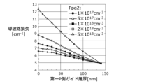
- FIG. 15 is a graph showing the relationship between the waveguide loss of the nitride-based semiconductor light emitting device according to Embodiment 1 and the film thickness of the first P-side guide layer.
- 16 is a graph showing the relationship between the effective refractive index difference ⁇ N of the nitride-based semiconductor light emitting device according to Embodiment 1 and the film thickness of the first P-side guide layer.
- FIG. 17 is a graph showing the relationship between the light confinement coefficient of the nitride-based semiconductor light emitting device according to Embodiment 1 and the film thickness of the first P-side guide layer.
- FIG. FIG. 18 is a graph schematically showing the bandgap energy distribution and the light intensity distribution in the stacking direction of the semiconductor stack of Example E02.
- FIG. 19 is a graph schematically showing the bandgap energy distribution and the light intensity distribution in the stacking direction of the semiconductor stack of Example E07.
- FIG. 20 is a graph showing the relationship between the bandgap energy in the AlxGa1 -xyInyN layer and the bandgap energy in the AlzGa1 -zN layer.
- FIG. 21 is a schematic side view showing warping of the substrate and the semiconductor laminate that occur when the semiconductor laminate is laminated on the substrate according to the first embodiment.
- FIG. 22 is a graph showing the relationship between the position in the lamination direction of the semiconductor laminate of Example E11 and the bandgap energy.
- FIG. 23 is a graph showing the relationship between the stress and the position in the stacking direction of the semiconductor stack of Example E11.
- FIG. 24 is a graph showing the relationship between the position in the stacking direction of the semiconductor laminate of Example E11 and the integrated stress.
- FIG. 25 is a graph showing the relationship between the position in the lamination direction of the semiconductor laminate of Example E12 and the bandgap energy.
- FIG. 26 is a graph showing the relationship between the stress and the position in the stacking direction of the semiconductor stack of Example E12.
- FIG. 27 is a graph showing the relationship between the position in the lamination direction of the semiconductor laminate of Example E12 and the integrated stress.
- FIG. 28 is a graph for explaining the composition required for the well layer of Example E13.
- FIG. 29 is a graph showing the relationship between the In composition ratio of the well layer and the lattice mismatch with respect to GaN.
- FIG. 30 is a graph schematically showing the bandgap energy distribution in the stacking direction of the semiconductor stack of Example E14.
- FIG. 31 is a graph schematically showing the bandgap energy distribution in the stacking direction of the semiconductor stack of Example E15.
- 32 is a schematic cross-sectional view showing the overall configuration of a nitride-based semiconductor light-emitting device according to Embodiment 2.
- FIG. 33 is a schematic cross-sectional view showing the overall configuration of a nitride-based semiconductor light-emitting device according to Embodiment 3.
- FIG. 33 is a schematic cross-sectional view showing the overall
- each figure is a schematic diagram and is not necessarily strictly illustrated. Therefore, the scales and the like are not always the same in each drawing.
- symbol is attached
- the terms “upper” and “lower” do not refer to vertical upper and vertical lower in absolute spatial recognition, but are defined by relative positional relationships based on the stacking order in the stacking structure. used as a term Also, the terms “above” and “below” are used not only when two components are spaced apart from each other and there is another component between the two components, but also when two components are spaced apart from each other. It also applies when they are arranged in contact with each other.
- Embodiment 1 A nitride-based semiconductor light-emitting device according to Embodiment 1 will be described.
- FIGS. 1, 2A and 2B are a schematic plan view and a cross-sectional view, respectively, showing the overall configuration of a nitride-based semiconductor light-emitting device 100 according to this embodiment.
- FIG. 2A shows a cross-section along line II-II of FIG.
- FIG. 2B is a schematic cross-sectional view showing the configuration of the active layer 104 included in the nitride-based semiconductor light emitting device 100 according to this embodiment.
- Each figure shows an X-axis, a Y-axis, and a Z-axis that are orthogonal to each other.
- the X, Y, and Z axes are a right-handed Cartesian coordinate system.
- the stacking direction of the nitride-based semiconductor light emitting device 100 is parallel to the Z-axis direction, and the main emission direction of light (laser light) is parallel to the Y-axis direction.
- the nitride-based semiconductor light-emitting device 100 includes a semiconductor laminate 100S including nitride-based semiconductor layers. Light is emitted from the end face 100F (see FIG. 1).
- the nitride-based semiconductor light-emitting device 100 is a semiconductor laser device having two facets 100F and 100R forming a resonator.
- the end surface 100F is a front end surface that emits laser light
- the end surface 100R is a rear end surface having a higher reflectance than the end surface 100F.
- the nitride-based semiconductor light emitting device 100 has a waveguide formed between the facet 100F and the facet 100R.
- the reflectances of the end faces 100F and 100R are 16% and 95%, respectively.
- the cavity length of nitride-based semiconductor light-emitting device 100 according to the present embodiment (that is, the distance between facet 100F and facet 100R) is about 1200 ⁇ m.
- the nitride-based semiconductor light emitting device 100 emits ultraviolet light having a peak wavelength in the 375 nm band, for example.
- Nitride-based semiconductor light emitting device 100 may emit ultraviolet light having a peak wavelength in a band other than the 375 nm band, or may emit light having a peak wavelength in a wavelength band other than ultraviolet light.
- the nitride-based semiconductor light emitting device 100 includes a substrate 101, a semiconductor laminate 100S, a current blocking layer 110, a P-side electrode 111, and an N-side electrode 112.
- the semiconductor laminate 100S includes an N-type cladding layer 102, an N-side guide layer 103, an active layer 104, a first P-side guide layer 105, an electron barrier layer 106, a second P-side guide layer 107, a P It has a mold cladding layer 108 and a contact layer 109 .
- the substrate 101 is a plate-like member that serves as a base for the nitride-based semiconductor light emitting device 100 .
- the substrate 101 is arranged below the N-type cladding layer 102 and is made of N-type GaN. More specifically, the substrate 101 is an 8500 nm thick GaN substrate doped with Si at a concentration of 1 ⁇ 10 18 cm ⁇ 3 .
- the N-type clad layer 102 is an N-type nitride semiconductor layer arranged above the substrate 101 .
- the N-type cladding layer 102 is a layer having a lower refractive index and a higher average bandgap energy than the active layer 104 .
- the N-type cladding layer 102 contains Al.
- the average Al composition ratio of the N-type cladding layer 102 is less than or equal to the average Al composition ratio of the P-type cladding layer 108 .
- the N-type cladding layer 102 is doped with Si at a concentration of 5 ⁇ 10 17 cm ⁇ 3 as an impurity.
- the average bandgap energy of a layer means the magnitude of the bandgap energy at a certain position in the stacking direction of the layer, from the position of the interface on the substrate side in the stacking direction of the layer to the substrate. It is the value of the bandgap energy integrated in the stacking direction up to the position of the interface on the far side and divided by the layer thickness (the distance between the interface on the substrate side and the interface on the far side from the substrate).
- the average refractive index of a layer is the magnitude of the refractive index at a certain position in the stacking direction of that layer, from the position of the interface on the side of the substrate in the stacking direction of that layer to the position of the interface on the far side from the substrate in the stacking direction. , and divided by the film thickness of the layer (the distance between the interface on the substrate side and the interface on the far side from the substrate).
- the average Al composition ratio of a layer means the magnitude of the Al composition ratio at a certain position in the lamination direction of the layer, from the position of the interface on the substrate side in the lamination direction of the layer to the position of the interface on the far side from the substrate. It is the value of the Al composition ratio integrated in the stacking direction and divided by the film thickness of the layer (the distance between the interface on the substrate side and the interface on the far side from the substrate).
- the average impurity concentration of a layer is the magnitude of the impurity concentration at a certain position in the stacking direction of that layer, from the position of the interface on the side of the substrate in the stacking direction of that layer to the position of the interface on the far side from the substrate in the stacking direction. , and divided by the layer thickness (the distance between the interface on the substrate side and the interface on the far side from the substrate).
- An impurity means an impurity doped to obtain an N-type conductivity in an N-type semiconductor layer, and an impurity doped to obtain a P-type conductivity in a P-type semiconductor layer.
- the N-side guide layer 103 is an optical guide layer arranged above the N-type cladding layer 102 and made of a nitride-based semiconductor.
- the N-side guide layer 103 has a higher refractive index and a lower bandgap energy than the N-type cladding layer 102 .
- the average bandgap energy of the N-side guide layer 103 is larger than the average bandgap energy of the first P-side guide layer 105 and smaller than the average bandgap energy of the second P-side guide layer 107 .
- the N-side guide layer 103 contains Al.
- the N-side guide layer 103 is an undoped nitride-based semiconductor layer.
- the average N-type impurity concentration of the N-side guide layer 103 is less than 1 ⁇ 10 18 cm ⁇ 3 .
- the N-type impurity concentration in each layer on the N-side and the P-type impurity concentration in each layer on the P-side are also simply referred to as impurity concentrations.
- the active layer 104 is arranged above the N-side guide layer 103 and is a light-emitting layer made of a nitride-based semiconductor.
- the active layer 104 has a quantum well structure and emits ultraviolet light.
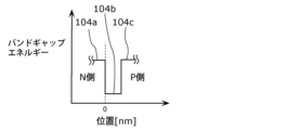
- the active layer 104 includes two barrier layers 104a and 104c and a well layer 104b disposed between the two barrier layers 104a and 104c.
- the configuration of the active layer 104 is not limited to this.
- active layer 104 may have a multiple quantum well structure.
- the active layer 104 may have three or more barrier layers and two or more well layers.
- Each of the barrier layers 104a and 104c is a nitride-based semiconductor layer arranged above the N-side guide layer 103 and functioning as a barrier for the quantum well structure.
- Barrier layer 104c is disposed above barrier layer 104a.
- the bandgap energy of each of the barrier layers 104a and 104c is equal to the bandgap energy of the well layer 104b, the average bandgap energy of the first P-side guide layer 105, and the average bandgap energy of the N-side guide layer 103. greater than the gap energy and less than the average bandgap energy of the electron barrier layer 106;
- the well layer 104b is a nitride-based semiconductor layer arranged above the barrier layer 104a and functioning as a well of a quantum well structure.
- the first P-side guide layer 105 is an optical guide layer arranged above the active layer 104 and made of a nitride-based semiconductor.
- the first P-side guide layer 105 has a higher refractive index and a lower bandgap energy than the P-type clad layer 108 .
- the first P-side guide layer 105 contains Al.
- the first P-side guide layer 105 is an undoped nitride semiconductor layer. In other words, the average impurity concentration of the first P-side guide layer 105 is less than 1 ⁇ 10 18 cm ⁇ 3 .
- the thickness of the first P-side guide layer 105 is thicker than the thickness of each of the two barrier layers 104a and 104c.
- the thickness of the first P-side guide layer 105 is thinner than the thickness of the second P-side guide layer 107 . Also, the average bandgap energy of the first P-side guide layer 105 is smaller than the bandgap energies of the barrier layers 104a and 104c.
- the electron barrier layer 106 is a nitride-based semiconductor layer arranged above the first P-side guide layer 105 .
- the bandgap energy of electron barrier layer 106 is greater than the bandgap energy of barrier layer 104c. This can suppress leakage of electrons from the active layer 104 to the P-type cladding layer 108 .
- the bandgap energy of the electron barrier layer 106 is greater than the bandgap energy of the P-type cladding layer 108 .
- the second P-side guide layer 107 is an optical guide layer arranged above the electron barrier layer 106 and made of a nitride-based semiconductor.
- the second P-side guide layer 107 has a higher refractive index and a lower bandgap energy than the P-type clad layer 108 .
- the average bandgap energy of the second P-side guide layer 107 is greater than the bandgap energy of the first P-side guide layer 105 .
- the second P-side guide layer 107 contains Al.
- the second P-side guide layer 107 is doped with impurities. In other words, the average impurity concentration of the second P-side guide layer 107 is 1 ⁇ 10 18 cm ⁇ 3 or more.
- the P-type clad layer 108 is arranged above the second P-side guide layer 107 and is a clad layer made of a P-type nitride semiconductor.
- the P-type clad layer 108 has a lower refractive index and a higher average bandgap energy than the active layer 104 .
- the average bandgap energy of the P-type cladding layer 108 is less than the average bandgap energy of the electron barrier layer 106 .
- the P-type cladding layer 108 contains Al.
- the P-type clad layer 108 is doped with Mg as an impurity.
- the impurity concentration at the end portion of the P-type cladding layer 108 closer to the active layer 104 is lower than the impurity concentration at the end portion farther from the active layer 104 .
- the P-type cladding layer 108 is an AlGaN layer with a thickness of 450 nm, and a P-type cladding layer with a thickness of 150 nm doped with Mg at a concentration of 2 ⁇ 10 18 cm ⁇ 3 located on the side closer to the active layer 104 . and a P-type AlGaN layer with a thickness of 300 nm doped with Mg at a concentration of 1 ⁇ 10 19 cm ⁇ 3 and disposed on the far side from the active layer 104 .
- a ridge 108R is formed in the P-type cladding layer 108 .
- the P-type cladding layer 108 is formed with two grooves 108T arranged along the ridge 108R and extending in the Y-axis direction.
- the ridge width W is approximately 30 ⁇ m.
- the distance between the lower end of the ridge 108R (that is, the bottom of the trench 108T) and the active layer 104 is dp.
- the distance between the lower end of the ridge 108R and the electron barrier layer 106) is dc.
- the contact layer 109 is a nitride-based semiconductor layer arranged above the P-type cladding layer 108 and in ohmic contact with the P-side electrode 111 .
- the contact layer 109 is a P-type GaN layer with a thickness of 60 nm.
- the contact layer 109 is doped with Mg at a concentration of 1 ⁇ 10 20 cm ⁇ 3 as an impurity.
- the current blocking layer 110 is an insulating layer arranged above the P-type cladding layer 108 and having transparency to light from the active layer 104 .
- the current blocking layer 110 is arranged in a region of the top surfaces of the P-type cladding layer 108 and the contact layer 109 other than the top surface of the ridge 108R.
- the current blocking layer 110 may also be arranged on a partial region of the upper surface of the ridge 108R.
- current blocking layer 110 may be disposed in the edge region of the top surface of ridge 108R.
- the current blocking layer 110 is a SiO2 layer.
- the P-side electrode 111 is a conductive layer arranged above the contact layer 109 .
- the P-side electrode 111 is arranged above the contact layer 109 and the current blocking layer 110 .
- the P-side electrode 111 is, for example, a single layer film or a multilayer film made of at least one of Cr, Ti, Ni, Pd, Pt, Ag and Au.
- Ag which has a low refractive index with respect to light with a wavelength of 375 nm, for at least a part of the P-side electrode 111 on the contact layer 109, leakage of light propagating through the waveguide to the P-side electrode 111 is suppressed. Since it can be made small, the waveguide loss generated at the P-side electrode 111 can be reduced.
- Ag has a refractive index of 0.5 or less in the wavelength range of 325 nm to 1500 nm, and a refractive index of 0.2 or less in the wavelength range of 360 nm to 950 nm.
- the effective refractive index of the inner region of the ridge 108R must be larger than the effective refractive index of the outer region. It is necessary to form the effective refractive index difference ( ⁇ N) so that Specifically, it is necessary to form SiO 2 having a refractive index lower than that of the P-type cladding layer 108 on the side wall of the ridge 108R to reduce the effective refractive index of the outer region of the ridge 108R.
- the film thickness of the P-type cladding layer 108 should be 0.15 ⁇ m or more.
- the N-side electrode 112 is a conductive layer arranged below the substrate 101 (that is, on the main surface opposite to the main surface on which the N-type cladding layer 102 and the like of the substrate 101 are arranged).
- the N-side electrode 112 is, for example, a single layer film or a multilayer film made of at least one of Cr, Ti, Ni, Pd, Pt and Au.
- the nitride-based semiconductor light emitting device 100 has a gap between the inner portion of the ridge 108R and the outer portion of the ridge 108R (the groove 108T portion), as shown in FIG. 2A.
- An effective refractive index difference ⁇ N is produced.
- the light generated in the portion of the active layer 104 below the ridge 108R can be confined in the horizontal direction (that is, in the X-axis direction).
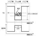
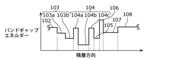
- FIG. 3 is a graph showing the distribution of the bandgap energy (Eg) and the refractive index in the stacking direction in the well layer and the barrier layer of a semiconductor light emitting device with a wavelength of 405 nm, which is longer than ultraviolet light.
- Eg bandgap energy
- FIG. 4 is a graph showing the distribution of the bandgap energy (Eg) and the refractive index in the stacking direction in the well layer and the barrier layer of a semiconductor light emitting device in the 375 nm band, which is an ultraviolet region.
- FIG. 5 is a graph showing distributions of effective refractive index and gain in the horizontal direction (corresponding to the X-axis direction in FIGS. 1 to 2B) of a 375 nm band semiconductor light emitting device.
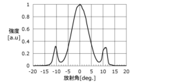
- FIG. 6 is a diagram showing a far-field pattern in the horizontal direction of a conventional ultraviolet semiconductor light-emitting device. The horizontal axis of FIG. 6 indicates the radiation angle in the horizontal direction, and the vertical axis indicates the light intensity.
- the difference ⁇ Ec between the conduction band potential energy and the electron quantum level energy of the barrier layer is relatively large. value (198 meV).
- the Fermi energy Ef of electrons is sufficiently smaller than the conduction band potential energy of the barrier layer, electrons can be prevented from leaking from the well layer to the P-side semiconductor layer over the barrier layer.
- the bandgap energy of the well layer is relatively large, so the difference ⁇ Ec between the conduction band potential energy and the electron quantum level energy of the barrier layer is small ( 67 meV).
- the Fermi energy Ef of electrons can be larger than the conduction band potential energy of the barrier layer, electrons easily leak from the well layer to the P-side semiconductor layer over the barrier layer.
- the number of carriers that cannot contribute to light emission in the well layer increases, so that the operating carrier density in the well layer increases.
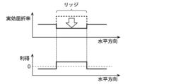
- the refractive index of the well layer decreases as the amplification gain in the well layer increases. Furthermore, as the carrier density in the current injection region of the well layer increases, the refractive index in the current injection region of the well layer decreases due to the plasma effect. Therefore, the refractive index of the current injection region of the well layer can be lower than the refractive index outside the current injection region of the well layer. For example, when the semiconductor light emitting device is a laser device having a ridge and current is injected into the ridge, as shown in FIG. obtain.
- the waveguide mechanism of the laser light propagating through the waveguide corresponding to the ridge of the semiconductor light emitting device becomes a refractive index anti-guiding gain waveguide mechanism.
- a portion of the laser light that propagates outside the current injection region (the region located below the ridge) in the well layer increases in proportion. A peak occurs, as shown.
- the oscillation threshold current value of the semiconductor light emitting device increases, and the heat saturation level decreases. In other words, the temperature characteristics of the laser element are degraded.
- kink a nonlinearly bent portion (so-called kink) may occur in a graph showing current-light output (IL) characteristics of a semiconductor light emitting device. In other words, the stability of light output from the semiconductor light emitting device is lowered.
- the nitride-based semiconductor light-emitting device 100 solves such problems of ultraviolet semiconductor light-emitting devices.
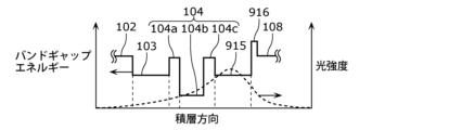
- FIGS. 7 to 9 are graphs schematically showing bandgap energy distributions and light intensity distributions in the lamination direction of semiconductor laminates according to Comparative Examples 1 and 2, respectively.
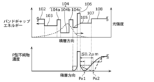
- FIG. 9 is a graph schematically showing the bandgap energy distribution and light intensity distribution of the semiconductor laminate 100S according to the present embodiment. 8 and 9 also show P-type impurity concentration distributions in the stacking direction of the semiconductor stacks according to Comparative Example 2 and the present embodiment, respectively.
- the semiconductor laminate according to Comparative Example 1 differs from the semiconductor laminate 100S according to the present embodiment in the configuration of the P-side guide layer 915.
- the electron barrier layer 916 is arranged between the P-side guide layer 915 and the P-type cladding layer 108 .
- the P-type cladding layer 108 has N
- the refractive index is larger than that of the mold cladding layer 102 .
- Mg which is a P-type impurity
- Si which is an N-type impurity.
- the P-type layer which forms the level, absorbs more light and has a higher refractive index. Therefore, as shown in FIG. 7, the peak position of the light intensity distribution is biased toward the P-type cladding layer 108 from the active layer 104 .
- the light confinement coefficient to the active layer 104 is reduced, and the operating carrier density is increased. Therefore, the refractive index of the well layer 104b is lowered.
- the semiconductor laminate according to Comparative Example 1 does not include the second P-side guide layer 107, in order to position the peak position of the light intensity distribution in the vertical direction in the vicinity of the active layer 104, It is necessary to increase the film thickness of the P-side guide layer 915 having a high refractive index. Therefore, the distance dp in the semiconductor laminate according to Comparative Example 1 is thicker than the distance dp according to the present embodiment. Therefore, the effective refractive index difference ⁇ N of the semiconductor laminate according to Comparative Example 1 is smaller than the effective refractive index difference ⁇ N according to the present embodiment. As a result, in the semiconductor laminate according to Comparative Example 1, the stability of the transverse mode of the laser light during operation is lowered.
- the semiconductor laminate according to Comparative Example 2 differs from the semiconductor laminate according to Comparative Example 1 in the arrangement of the electron barrier layer 926 and the P-side guide layer 925 .
- the positions of the electron barrier layer 926 and the P-side guide layer 925 in the lamination direction are the same as those of the electron barrier layer 916 and the P-side guide layer 925 in the semiconductor laminate according to Comparative Example 1.
- the position in the stacking direction with the side guide layer 915 is switched.
- a first P having a small bandgap energy (that is, having a large refractive index) is placed between the active layer 104 and the electron barrier layer 106.
- a side guide layer 105 is provided. Furthermore, the average bandgap energy of the first P-side guide layer 105 is smaller than the average bandgap energy of the second P-side guide layer 107, and the average refractive index of the first P-side guide layer 105 is lower than that of the second P-side guide layer 105. larger than layer 107.
- the peak position of the light intensity distribution can be brought closer to the active layer 104 than in the semiconductor laminates according to the first and second comparative examples.
- the first P-side guide layer 105 is a nitride-based semiconductor layer with an average impurity concentration of less than 1 ⁇ 10 18 cm ⁇ 3 , specifically 7 ⁇ 10 17 cm ⁇ 3 (see FIG. 9), Free carrier loss in one P-side guide layer 105 can be reduced. Therefore, in the present embodiment, in the light intensity distribution in the stacking direction, the proportion of the light distribution existing in the undoped region near the active layer 104 and in the first P-side guide layer 105 having a low impurity concentration increases, resulting in free carrier loss.
- FIG. 9 shows the case where the impurity concentration of the first P-side guide layer 105 is constant in the stacking direction, but the impurity concentration may monotonically increase with increasing distance from the active layer 104 in the stacking direction. .
- the impurity concentration in the region near the active layer 104 where the light intensity is high can be made relatively lower than the impurity concentration in the region far from the active layer 104. Free carrier loss can be reduced while suppressing an increase in series resistance of the light emitting element 100 .
- the second P-side guide layer 107 of the semiconductor stacked body 100S is doped with impurities. As a result, the electric resistance of the semiconductor stacked body 100S can be reduced, so that the operating voltage of the nitride-based semiconductor light emitting device 100 can be reduced. In addition, since the second P-side guide layer 107 is farther from the active layer 104 than the first P-side guide layer 105, the light distribution intensity in the vertical direction is reduced, and the average impurity concentration of the second P-side guide layer 107 is is higher than the average impurity concentration of the first P-side guide layer 105, the free carrier loss in the second P-side guide layer 107 can be suppressed.
- the film thickness of the first P-side guide layer 105 is made thinner than the film thickness of the second P-side guide layer 107, thereby reducing the distance dp. Therefore, in this embodiment, the effective refractive index difference ⁇ N can be increased. Therefore, the light confinement factor to the waveguide of the nitride-based semiconductor light emitting device 100 can be increased. As a result, in the nitride-based semiconductor light-emitting device 100, the horizontal transverse mode of the laser light can be stably confined in the waveguide, so that the occurrence of kinks in the current-optical output characteristics can be suppressed.
- the total thickness of the first P-side guide layer 105 and the second P-side guide layer 107 is equal to or greater than the thickness of the N-side guide layer 103 . This makes it possible to further increase the distance dc, so that it is possible to further increase the effective refractive index difference ⁇ N and the light confinement coefficient.
- the average Al composition ratio of the second P-side guide layer 107 is made larger than the average Al composition ratio of the first P-side guide layer 105, so that the average band of the second P-side guide layer 107 is
- the gap energy is made larger than the average bandgap energy of the first P-side guide layer 105 .
- the average refractive index of the first P-side guide layer 105 can be made larger than that of the second P-side guide layer 107, so that the peak position of the light intensity distribution can be brought closer to the active layer 104. Therefore, in this embodiment, the waveguide loss of the nitride-based semiconductor light emitting device 100 can be reduced.
- FIG. 10 is a diagram showing the main configuration of Examples E01 to E03 and Comparative Examples C01 to C06 and the results of characteristic calculations.
- FIG. 11 is a diagram showing the main configuration of Examples E04 to E06 and Comparative Examples C11 to C16, and the results of characteristic calculations.
- FIG. 12 is a diagram showing the main configuration and characteristic calculation results of Comparative Examples C02, C12, and C21 to C26. In FIGS.
- FIG. 13 is a graph showing coordinates of positions in the stacking direction of the nitride-based semiconductor light emitting device 100 according to this embodiment. As shown in FIG.
- the coordinates of the position of the end surface of the active layer 104 on the N side of the well layer 104b, that is, the end surface of the well layer 104b closer to the N-side guide layer 103 in the stacking direction is set to zero, and downward ( The direction toward the N-side guide layer 103) is the negative direction of the coordinates, and the upward direction (the direction toward the first P-side guide layer 105) is the positive direction of the coordinates.
- Example E01 will be described.
- the nitride-based semiconductor light-emitting device 100 of Example E01 has the following configuration (see FIG. 10).
- the N-type cladding layer 102 is an N-type Al 0.065 Ga 0.935 N layer with a thickness of 800 nm doped with Si at a concentration of 5 ⁇ 10 17 cm ⁇ 3 .
- the N-side guide layer 103 is an undoped Al 0.03 Ga 0.97 N layer with a thickness of 180 nm.
- Each of the barrier layers 104a and 104c is an undoped Al 0.04 Ga 0.96 N layer with a thickness of 10 nm.
- the well layer 104b is an undoped In 0.01 Ga 0.99 N layer with a thickness of 17.5 nm.
- the first P-side guide layer 105 is an undoped Al 0.02 Ga 0.98 N layer with a thickness of 56 nm.
- the electron barrier layer 106 is a 5 nm thick P-type Al 0.36 Ga 0.64 N layer doped with Mg at a concentration of 1 ⁇ 10 19 cm ⁇ 3 .
- the second P-side guide layer 107 is a P-type Al 0.04 Ga 0.96 N layer with a thickness of 124 nm doped with Mg at a concentration of 1 ⁇ 10 18 cm ⁇ 3 .
- the P-type clad layer 108 is a P-type Al 0.065 Ga 0.935 N layer with a thickness of 450 nm.
- the P-type clad layer 108 is a P-type Al 0.04 Ga 0.96 N layer.
- the P-type cladding layer 108 includes a P-type Al 0.065 Ga 0.935 N layer with a thickness of 150 nm doped with Mg at a concentration of 2 ⁇ 10 18 cm ⁇ 3 and disposed on the side closer to the active layer 104 . and a 300 nm thick P-type Al 0.065 Ga 0.935 N layer doped with Mg at a concentration of 1 ⁇ 10 19 cm ⁇ 3 located on the far side from the layer 104 .
- the contact layer 109 is a 100 nm thick P-type GaN layer doped with Mg at a concentration of 1 ⁇ 10 20 cm ⁇ 3 .
- Comparative Examples C01 to C06 configurations not shown in FIG. 10 are the same as those of Example E01.
- the nitride-based semiconductor light-emitting devices of Comparative Examples C02 and C06 have the Al composition ratio (Xpg1) of the first P-side guide layer and the Al composition ratio (Xpg2) of the second P-side guide layer. It differs from E01 and matches in other configurations.
- the average bandgap energy of the second P-side guide layer is the average of the first P-side guide layer. equal to the bandgap energy.
- the Al composition ratio of the second P-side guide layer is smaller than the Al composition ratio of the first P-side guide layer, so the average band of the second P-side guide layer
- the gap energy is less than the average bandgap energy of the first P-side guide layer.
- the Al composition ratio of the second P-side guide layer 107 is higher than the Al composition ratio of the first P-side guide layer 105, so the second P-side guide The average bandgap energy of the layer is greater than the average bandgap energy of the first P-side guiding layer. Comparing the characteristic calculation results of Example E01 shown in FIG.
- Example E01 the average band gap energy of the second P-side guide layer 107 is 105 (that is, the refractive index of the first P-side guide layer 105 is higher than that of the second P-side guide layer 107), the light distribution in the stacking direction is It can be seen that the light confinement factor can be increased and the waveguide loss can be reduced because the proportion of light existing in the nearby undoped region and the low impurity concentration first P-side guide layer 105 increases.
- FIG. 14 and 15 respectively show the relationship between the operating voltage and the waveguide loss when the nitride-based semiconductor light emitting device 100 according to the present embodiment is operated at 200 mA, and the film thickness of the first P-side guide layer 105.
- FIG. 14 is a graph showing 14 and 15, the total film thickness of the first P-side guide layer 105 and the second P-side guide layer 107 of the nitride-based semiconductor light emitting device 100 according to Comparative Example C01 is 140 nm, and the first P-side guide layer The operating voltage and waveguide loss are shown for varying the film thickness of 105, respectively. 14 and 15 respectively show the results when the average impurity concentration (average Mg concentration) in the second P-side guide layer 107 is changed from 1 ⁇ 10 17 cm ⁇ 3 to 5 ⁇ 10 18 cm ⁇ 3 . Operating voltages and waveguide losses are indicated.
- 16 and 17 are graphs showing the relationship between the effective refractive index difference ⁇ N and the optical confinement coefficient of the nitride-based semiconductor light emitting device 100 according to the present embodiment, and the film thickness of the first P-side guide layer 105, respectively. is.
- the operating voltage can be reduced by setting the average impurity concentration of the second P-side guide layer 107 to 5 ⁇ 10 17 cm ⁇ 3 or higher.
- the waveguide loss can be reduced by setting the average impurity concentration of the second P-side guide layer 107 to 2 ⁇ 10 18 cm ⁇ 3 or less. Therefore, by setting the average impurity concentration of the second P-side guide layer 107 to 5 ⁇ 10 17 cm ⁇ 3 or more and 2 ⁇ 10 18 cm ⁇ 3 or less, both the operating voltage and the waveguide loss can be reduced. Furthermore, by setting the average impurity concentration of the second P-side guide layer 107 to 1 ⁇ 10 18 cm ⁇ 3 or less, the waveguide loss can be further reduced.
- the effective refractive index difference becomes ⁇ N increases.
- the electron barrier layer 106 having a high Al composition and a low refractive index approaches the active layer 104, so that the optical confinement factor is lowered.
- the Al composition ratio of the first P-side guide layer 105 is set lower than the Al composition ratio of the second P-side guide layer 107.
- the optical confinement coefficient can be increased.
- the operating voltage can be reduced by setting the average impurity concentration of the second P-side guide layer 107 to 5 ⁇ 10 17 cm ⁇ 3 or higher.
- the waveguide loss can be reduced by setting the average impurity concentration of the second P-side guide layer 107 to 2 ⁇ 10 18 cm ⁇ 3 or less. Therefore, by setting the average impurity concentration of the second P-side guide layer 107 to 5 ⁇ 10 17 cm ⁇ 3 or more and 2 ⁇ 10 18 cm ⁇ 3 or less, the effect of reducing both the operating voltage and the waveguide loss can be obtained. can be done. Furthermore, by setting the average impurity concentration of the second P-side guide layer 107 to 1 ⁇ 10 18 cm ⁇ 3 or less, the waveguide loss can be further reduced to 4.91 cm ⁇ 1 .
- the film thickness of the second P-side guide layer 107 is made thicker than the film thickness of the first P-side guide layer 105, and the average impurity concentration of the second P-side guide layer 107 is set to By making it 5 ⁇ 10 17 cm ⁇ 3 or more and 2 ⁇ 10 18 cm ⁇ 3 or less, it is possible to increase the effective refractive index difference ⁇ N, reduce the operating voltage, and reduce the waveguide loss.
- a high effective refractive index difference ⁇ N of 17.67 ⁇ 10 ⁇ 3 equal to or greater than 1 ⁇ 10 ⁇ 2 can be realized.
- a refractive index anti-guiding type gain guiding mechanism is likely to occur due to a decrease in the refractive index of the well layer due to an increase in the operating carrier density.
- the ⁇ N determined by the waveguide structure is 1 ⁇ 10 ⁇ 2 or more in the absence of current injection, the well layer refractive index decreases due to the increase in the operating carrier density of the well layer during the laser oscillation operation, resulting in an effective reduction during the laser oscillation operation.
- Such a high effective refractive index difference ⁇ N of 1 ⁇ 10 ⁇ 2 or more is obtained in the semiconductor multilayer body 100S according to the present embodiment because the first P-side guide layer 105 and the second P-side guide layer 107 This is because the distance dp between the electron barrier layer 106 and the active layer 104 can be reduced as a result of forming the electron barrier layer 106 at .
- Example E02 will be described.
- the nitride-based semiconductor light-emitting device 100 of Example E02 is different from the nitride-based semiconductor light-emitting device 100 of Example E01 in the film thicknesses of the N-side guide layer 103, the first P-side guide layer 105, and the second P-side guide layer 107.
- the film thickness (Tng) of the N-side guide layer 103 in Example E02 was 140 nm
- the film thickness (Tpg1) of the first P-side guide layer 105 was 72 nm
- the film thickness (Tpg2) of 107 is 148 nm.
- Example E02 the total film thickness of the first P-side guide layer 105 and the second P-side guide layer 107 is thicker than the film thickness of the N-side guide layer 103.
- FIG. 10 The effect of this configuration will be described using comparative examples C01 to C03.
- the total thickness of the first P-side guide layer and the second P-side guide layer is greater than the thickness (Tng) of the N-side guide layer. too thin.
- the total thickness of the first P-side guide layer and the second P-side guide layer is equal to the thickness of the N-side guide layer.
- the total film thickness of the first P-side guide layer and the second P-side guide layer is thicker than the film thickness of the N-side guide layer.
- the effective refractive index difference ⁇ N increases.
- the total thickness of the first P-side guide layer 105 and the second P-side guide layer 107 is equal to the thickness of the N-side guide layer 103. Since it is thicker, the effective refractive index difference ⁇ N can be increased.
- FIG. 18 is a graph schematically showing the bandgap energy distribution and the light intensity distribution in the stacking direction of the semiconductor stack 100S of Example E02.
- FIG. 18 also shows an example of P-type impurity concentration distribution in the stacking direction of the semiconductor stack 100S of Example E02.
- the average impurity (Mg) concentration of the first P-side guide layer 105 is less than 1.0 ⁇ 10 18 cm ⁇ 3 .
- the impurity concentration of the first P-side guide layer 105 may increase with increasing distance from the active layer 104.
- the impurity concentration can be reduced in the region of the first P-side guide layer 105 near the active layer 104, that is, the region where the light intensity is high, and the region of the first P-side guide layer 105 far from the active layer 104, That is, the impurity concentration can be increased in the region where the light intensity is low. Therefore, it is possible to achieve both a reduction in waveguide loss and a reduction in operating voltage of the nitride-based semiconductor light emitting device 100 .
- the average impurity concentration of the first P-side guide layer 105 may be 1.0 ⁇ 10 17 cm ⁇ 3 or more and less than 1.0 ⁇ 10 18 cm ⁇ 3 .
- the average impurity concentration of the second P-side guide layer 107 is 1.0 ⁇ 10 18 cm ⁇ 3 or more.
- the impurity concentration of the second P-side guide layer 107 may increase with increasing distance from the active layer 104 .
- the impurity concentration can be reduced in the region of the second P-side guide layer 107 close to the active layer 104, that is, the region where the light intensity is high, and the region of the second P-side guide layer 107 far from the active layer 104, That is, the impurity concentration can be increased in the region where the light intensity is low.
- the average impurity concentration is 1.0 ⁇ 10 18 cm ⁇ 3 or more and 3.0 ⁇ 10 18 cm ⁇ 3 or less. may be 1.0 ⁇ 10 19 cm ⁇ 3 or more and 1.0 ⁇ 10 20 cm ⁇ 3 or less.
- the activation rate of Mg which is an impurity
- Mg diffuses into the second P-side guide layer 107 as the electron barrier layer 106 is heavily doped with Mg, as shown in FIG. , the impurity concentration increases, and the impurity concentration decreases toward the position (Px1 or Px2) where the impurity concentration is minimum from the interface.
- the electron barrier layer 106 to the P-type clad layer 108 are changed from the electron barrier layer 106 to the P-type clad layer 108 as shown in the P-type impurity concentration distribution example (solid line and broken line) shown in FIG.
- Px1 or Px2 where the impurity concentration is minimum at a distance of 0.2 ⁇ m or less in the stacking direction toward (that is, upward), and the impurity concentration monotonously increases upward from this position.
- the impurity concentration in the region near the active layer 104 in the second P-side guide layer 107 and the P-type cladding layer 108 can be reduced, thereby suppressing an increase in waveguide loss.
- the position where the impurity concentration is minimum may be located in the second P-side guide layer 107 or may be located in the P-type cladding layer 108 .
- the lower the Al composition ratio in the AlGaN layer having an Al composition ratio of 6% or less the more the effect of light absorption loss between the impurity level of Mg used as a P-type impurity and the conduction band. increases. Therefore, by making the Mg concentration in the AlGaN layer with an Al composition ratio of 6% or less as low as possible, the effects of free carrier loss and light absorption loss via the impurity level of Mg can be reduced.
- the second P-side guide layer 107 preferably has a region in which the Mg concentration decreases with increasing distance from the active layer 104 . This can reduce the effects of free carrier loss due to Mg doping and light absorption loss through the impurity level of Mg.
- Example E03 will be described.
- the nitride-based semiconductor light-emitting device 100 of Example E03 differs from the nitride-based semiconductor light-emitting device 100 of Example E02 in the Al composition ratio (Xnc) of the N-type cladding layer 102 (see FIG. 10).
- the Al composition ratio of the N-type cladding layer 102 of Example E03 is 4.5%.
- the average Al composition ratio of the N-type clad layer 102 is smaller than the average Al composition ratio of the P-type clad layer 108 .
- Comparative Examples C04, C02, and C05 As shown in FIG. 10, in the nitride-based semiconductor light emitting device of Comparative Example C04, the average Al composition ratio of the N-type clad layer is smaller than the average Al composition ratio of the P-type clad layer. In the nitride-based semiconductor light emitting device of Comparative Example C02, the average Al composition ratio of the N-type clad layer is equal to the average Al composition ratio of the P-type clad layer. In the nitride-based semiconductor light emitting device of Comparative Example C05, the average Al composition ratio of the N-type clad layer is larger than the average Al composition ratio of the P-type clad layer.
- the average Al composition ratio of the N-type clad layer becomes smaller than the average Al composition ratio of the P-type clad layer, the average refractive index of the N-type clad layer can be increased. Therefore, the peak position of the light intensity distribution in the stacking direction of the nitride-based semiconductor light emitting device (that is, the vertical light distribution peak position shown in FIG. 10) is prevented from being excessively biased in the direction from the active layer toward the P-type cladding layer. can. As a result, as shown in the characteristic calculation results of Comparative Examples C04, C02, and C05 in FIG. , the waveguide loss can be reduced.
- the average Al composition ratio of the N-type cladding layer 102 is smaller than the average Al composition ratio of the P-type cladding layer 108, so the waveguide loss can be reduced.
- Example E04 will be described.
- the nitride-based semiconductor light-emitting device 100 of Example E04 differs from Example E01 in the Al composition ratio of each layer, but is the same in other configurations.
- the N-type cladding layer 102, N-side guide layer 103, each barrier layer, first P-side guide layer 105, second P-side guide layer 107, and The Al composition ratios of the P-type cladding layer 108 are 10%, 5%, 7%, 4%, 6% and 10%, respectively.
- Comparative Examples C11 to C16 configurations not shown in FIG. 11 are the same as those of Example E04.
- the nitride-based semiconductor light-emitting devices of Comparative Examples C12 and C16 differ from Example E04 in the Al composition ratio of the first P-side guide layer and the Al composition ratio of the second P-side guide layer. matches in In Comparative Example C12, since the compositions of the first P-side guide layer and the second P-side guide layer are the same, the average bandgap energy of the second P-side guide layer is the average of the first P-side guide layer. equal to the bandgap energy.
- the Al composition ratio of the second P-side guide layer is smaller than the Al composition ratio of the first P-side guide layer, so the average band of the second P-side guide layer
- the gap energy is less than the average bandgap energy of the first P-side guide layer.
- the Al composition ratio of the second P-side guide layer 107 is higher than the Al composition ratio of the first P-side guide layer 105, so the second P-side guide The average bandgap energy of the layer is greater than the average bandgap energy of the first P-side guiding layer. Comparing the characteristic calculation results of Example E04 shown in FIG.
- the light distribution in the stacking direction is It can be seen that the optical confinement factor can be increased and the waveguide loss can be reduced because the proportion of light existing in the nearby undoped region and the low impurity concentration first P-side guide layer 105 increases.
- the nitride-based semiconductor light-emitting devices of Comparative Examples C21 to C23 shown in FIG. 12 differ from Comparative Example C02 in the Al composition ratio (Xng, Xpg1, and Xpg2) of each guide layer, and are identical in other configurations. .
- the Al composition ratio of each guide layer was 2%, 4%, and 5%, respectively.
- Comparative Example C12 differs from Comparative Example C12 in the Al composition ratio (Xng, Xpg1, and Xpg2) of each guide layer, but are identical in other configurations. .
- the Al composition ratios of the respective guide layers are 4%, 6%, and 7%, respectively.
- the Al composition ratio of each cladding layer is 6.5%, and the Al composition ratio of each guide layer is 4%.
- the deviation of the vertical light distribution peak position from the active layer toward the P-type cladding layer becomes large, resulting in an increase in waveguide loss.
- the Al composition ratio of each cladding layer is 10%, and the Al composition ratio of each guide layer is 6%. In the above case, the deviation of the vertical light distribution peak position from the active layer toward the P-type cladding layer becomes large, resulting in an increase in waveguide loss.
- the average Al composition ratio of the N-side guide layer 103, the average Al composition ratio of the first P-side guide layer 105, and the average Al composition ratio of the second P-side guide layer 107 are It may be 60% or less of the average Al composition ratio of the P-type cladding layer 108 .
- the vertical light distribution peak position can be brought closer to the center of the lamination direction of the active layer 104, so that the waveguide loss can be reduced.
- the average Al composition ratio of each guide layer may be 50% or less of the average Al composition ratio of the P-type cladding layer 108 . Thereby, the waveguide loss can be further reduced.
- the average Al composition ratio of the N-side guide layer 103, the average Al composition ratio of the first P-side guide layer 105, and the average Al composition ratio of the second P-side guide layer 107 are each set to 1.5. % or more.
- the Al composition ratio of each guide layer is the same value.
- the distribution peak position can be brought closer to the center of the active layer in the stacking direction. Therefore, waveguide loss can be further reduced.
- the average Al The average composition ratio (that is, the average value of Xng, Xpg1, and Xpg2) may be 60% or less or 50% or less of the average Al composition ratio of the P-type cladding layer 108 . Thereby, the waveguide loss can be further reduced.
- the average Al composition ratio of the N-side guide layer 103, the average Al composition ratio of the first P-side guide layer 105, and the average Al composition ratio of the second P-side guide layer 107 are too small, the above three problems occur during the laser oscillation operation.
- the difference between the Fermi energy of electrons in the layer and the conduction band potential becomes smaller, the electron concentration increases, and the free carrier loss increases.
- the average Al composition ratio of the N-side guide layer 103, the average Al composition ratio of the first P-side guide layer 105, and the average Al composition ratio of the second P-side guide layer 107 are each set to 1.5. % or more.
- the N-side guide layer 103, the first P-side guide layer 105, and the second P-side guide layer 105 The average value of the average Al composition ratio of the side guide layer 107 (that is, the average value of Xng, Xpg1, and Xpg2) is the average value of the average Al composition ratios of the N-type clad layer 102 and the P-type clad layer 108 (that is, Xnc and the average value of Xpc) may be 60% or less or 50% or less.
- the average Al composition ratio of the N-side guide layer 103, the average Al composition ratio of the first P-side guide layer 105, and the average Al composition ratio of the second P-side guide layer 107 are each set to 1.5. % or more.
- Example E05 will be described.
- the nitride-based semiconductor light-emitting device 100 of Example E05 is different from the nitride-based semiconductor light-emitting device 100 of Example E04 in the film thicknesses of the N-side guide layer 103, the first P-side guide layer 105, and the second P-side guide layer 107. (see FIG. 11).
- the thickness of the N-side guide layer 103 in Example E05 is 140 nm
- the thickness of the first P-side guide layer 105 is 72 nm
- the thickness of the second P-side guide layer 107 is 148 nm. is.
- Example E05 the total film thickness of the first P-side guide layer 105 and the second P-side guide layer 107 is thicker than the film thickness of the N-side guide layer.
- the effects of this configuration will be described using comparative examples C11 to C13.
- the total film thickness of the first P-side guide layer and the second P-side guide layer is thinner than the film thickness of the N-side guide layer.
- the total thickness of the first P-side guide layer and the second P-side guide layer is equal to the thickness of the N-side guide layer.
- the total film thickness of the first P-side guide layer and the second P-side guide layer is thicker than the film thickness of the N-side guide layer.
- the effective refractive index difference ⁇ N increases.
- the total thickness of the first P-side guide layer 105 and the second P-side guide layer 107 was equal to the thickness of the N-side guide layer 103. Since it is thicker, the effective refractive index difference ⁇ N can be increased.
- Example E06 will be described.
- the nitride-based semiconductor light-emitting device 100 of Example E06 differs from the nitride-based semiconductor light-emitting device 100 of Example E05 in the Al composition ratio of the N-type cladding layer 102 (see FIG. 11).
- the Al composition ratio of the N-type cladding layer 102 of Example E06 is 8%.
- the average Al composition ratio of the N-type clad layer 102 is smaller than the average Al composition ratio of the P-type clad layer 108 .
- Comparative Example C14 Comparative Example C12
- Comparative Example C15 Comparative Example C15
- the average Al composition ratio of the N-type clad layer is smaller than the average Al composition ratio of the P-type clad layer.
- the average Al composition ratio of the N-type clad layer is equal to the average Al composition ratio of the P-type clad layer.
- the average Al composition ratio of the N-type clad layer is larger than the average Al composition ratio of the P-type clad layer.
- the average Al composition ratio of the N-type clad layer becomes smaller than the average Al composition ratio of the P-type clad layer, the average refractive index of the N-type clad layer can be increased. Therefore, it is possible to prevent the peak position of the light intensity distribution (vertical light distribution peak position) in the stacking direction of the nitride-based semiconductor light emitting device from being excessively biased in the direction from the active layer toward the P-type clad layer. As a result, as shown in the characteristic calculation results of Comparative Examples C14, C12, and C15 in FIG. , the waveguide loss can be reduced.
- the average Al composition ratio of the N-type cladding layer 102 is smaller than the average Al composition ratio of the P-type cladding layer 108, so the waveguide loss can be reduced.
- Example E07 will be described with reference to FIG. FIG. 19 is a graph schematically showing the bandgap energy distribution and the light intensity distribution in the stacking direction of the semiconductor stack 100S of Example E07.
- Example E07 includes a region in which the Al composition ratios of the first P-side guide layer 105 and the second P-side guide layer 107 monotonically increase as the distance from the active layer 104 increases. It is different from Example E01 and is the same in other configurations.
- the first P-side guide layer 105 and the second P-side guide layer 107 include bandgap gradient regions in which the bandgap energy increases as the distance from the active layer 104 increases.
- the configuration in which the Al composition ratio monotonously increases includes a configuration in which there is a region in which the Al composition ratio is constant in the stacking direction.
- a configuration in which the Al composition ratio increases stepwise is also included.
- the Al composition ratios of the first P-side guide layer 105 and the second P-side guide layer 107 are represented by Xpg1 and Xpg2, respectively.
- the Al composition ratios Xpg1 near and far from the active layer 104 of the first P-side guide layer 105 are 1.5% and 2.5%, respectively.
- the Al composition ratios Xpg2 near and far from the active layer 104 of the second P-side guide layer 107 are 3.5% and 4.5%, respectively.
- the refractive index of each layer increases as it approaches the active layer 104. can therefore be increased. Therefore, since the refractive index of the region near the active layer 104 in the first P-side guide layer 105 and the second P-side guide layer 107 can be increased, the peak position of the light intensity distribution in the lamination direction is shifted from the active layer 104 to the P-type. Excessive deviation toward the cladding layer 108 can be suppressed. Thereby, waveguide loss can be reduced.
- the optical confinement factor was 5.52%
- the effective refractive index difference ⁇ N was 20.9 ⁇ 10 ⁇ 3
- the waveguide loss was 4.71 cm ⁇ 1
- the vertical light distribution peak A nitride-based semiconductor light-emitting device 100 with a position of 15.1 nm can be realized.
- Example E08 will be described.
- Example E08 is different from Example E04 in that the Al composition ratio of the first P-side guide layer 105 and the second P-side guide layer 107 includes a region in which the Al composition ratio increases monotonically as the distance from the active layer 104 increases. match in the configuration of In other words, in Example E08, the first P-side guide layer 105 and the second P-side guide layer 107 include bandgap gradient regions in which the bandgap energy increases as the distance from the active layer 104 increases.
- the Al composition ratios of the first P-side guide layer 105 and the second P-side guide layer 107 are represented by Xpg1 and Xpg2, respectively.
- the Al composition ratios Xpg1 near and far from the active layer 104 of the first P-side guide layer 105 are 3.5% and 4.5%, respectively.
- the Al composition ratios Xpg2 near and far from the active layer 104 of the second P-side guide layer 107 are 5.5% and 6.5%, respectively.
- Example E08 as in Example E07, in the first P-side guide layer 105 and the second P-side guide layer 107, the Al composition ratio was monotonously increased as the distance from the active layer 104 increased. Therefore, it is possible to prevent the peak position of the light intensity distribution in the stacking direction from being excessively biased in the direction from the active layer 104 toward the P-type cladding layer 108 . Thereby, waveguide loss can be reduced.
- both the first P-side guide layer 105 and the second P-side guide layer 107 included the bandgap gradient region, but the first P-side guide layer 105 and the second P-side guide layer 105 At least one of the side guiding layers 107 may include a bandgap graded region. Similar effects can also be achieved with such a configuration.
- the optical confinement factor was 6.06%
- the effective refractive index difference ⁇ N was 22.1 ⁇ 10 ⁇ 3
- the waveguide loss was 4.37 cm ⁇ 1
- the vertical light distribution peak A nitride-based semiconductor light emitting device 100 with a position of 13.2 nm can be realized.
- Example E09 will be described.
- Example E09 is different from Example E02 in that the first P-side guide layer 105 contains Al and In, and is the same as Example E02 in other respects.
- the composition of the first P - side guide layer 105 is Al0.04Ga0.9516In0.0084N .
- the first P-side guide layer 105 containing Al and In makes it possible to independently control the bandgap energy and lattice constant of the first P-side guide layer 105 .
- FIG. 20 is a graph showing the relationship between the bandgap energy in the AlxGa1 -xyInyN layer and the bandgap energy in the AlzGa1 -zN layer.
- the horizontal axis indicates the In composition ratio y in the Al x Ga 1-x-y In y N layer
- the vertical axis indicates the Al composition ratio x in the Al x Ga 1-x-y In y N layer. show.
- the Al composition ratio z of the Al z Ga 1-z N layer is 0, 0.05, 0.10, 0.15, 0.20, 0.25, 0.30, 0.35. , and 0.40.
- the relationship between the In composition ratio y and the Al composition ratio x for equalizing the lattice constant of the Al x Ga 1-xy In y N layer and the lattice constant of the GaN layer is indicated by a dashed line. It is shown.
- the region above (or to the left of) the dashed line in the graph of FIG . or right) indicates a composition in which the lattice constant of the Al x Ga 1-xy In y N layer is larger than the lattice constant of the GaN layer.
- lattice constants 0.311 nm, 0.3182 nm, and 0.354 nm are used as the lattice constants of AlN, GaN, and InN, respectively.
- the first P-side guide layer 105 made of the AlGaN layer in each of the above examples can be replaced with the first P-side guide layer 105 made of the AlGaInN layer without changing the bandgap energy.
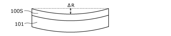
- FIG. 21 is a schematic side view showing warpage of the substrate 101 and the semiconductor laminate 100S that occurs when the semiconductor laminate 100S is laminated on the substrate 101 according to the present embodiment.
- the substrate 101 and the semiconductor are deformed due to tensile strain on the substrate 101 caused by the AlGaN layer in the semiconductor laminate 100S.
- a warp occurs in the laminated body 100S.
- the upper surface of the semiconductor stacked body 100S is warped in a concave shape.
- the amount of warp when the upper surface of the semiconductor stacked body 100S is concave is represented by a negative numerical value.
- the warp amount (that is, the height of the convex portion) when the top surface of the semiconductor stacked body 100S is convex is represented by a positive numerical value.
- Example E09 by adjusting the In composition ratio y and the Al composition ratio x of the first P-side guide layer 105, the lattice constant of the first P-side guide layer 105 can be adjusted independently of the bandgap energy. Tensile distortion of the one P-side guide layer 105 with respect to the substrate 101 can be reduced. Therefore, warping of the nitride-based semiconductor light emitting device 100 can be reduced. As a result, when the semiconductor laminate 100S is stacked on the GaN wafer serving as the base material of the substrate 101 and processed, the occurrence of wafer breakage and cracks in the wafer can be suppressed.
- the optical confinement factor was 5.62%
- the effective refractive index difference ⁇ N was 19.6 ⁇ 10 ⁇ 3
- the waveguide loss was 4.90 cm ⁇ 1
- the vertical light distribution peak A nitride-based semiconductor light-emitting device 100 with a position of 14.3 nm can be realized.
- Example E09 only the first P-side guide layer 105 contained Al and In, but the N-side guide layer 103, the second P-side guide layer 107, and the P-type clad layer 108 also contained Al and In. may contain. Even in such a configuration, as in Example E01 and the like, the bandgap energy Eng of the N-side guide layer 103, the bandgap energy Epg1 of the first P-side guide layer 105, and the bandgap energy Epg1 of the second P-side guide layer 107 Between the gap energy Epg2 and the bandgap energy Epc of the P-type cladding layer 108, the following equations (2) and (3) can be established.
- the bandgap energy increases.
- the bandgap energy becomes larger than the bandgap energy of the Al x Ga 1-xy In y N layer.
- the bandgap energy Epg1 of the first P-side guide layer 105 can be made smaller than the bandgap energy Epg2 of the second P-side guide layer 107.
- the refractive index of the first P-side guide layer 105 can be maximized, so that the vertical light distribution
- the peak position can be brought close to the center of the active layer 104 in the stacking direction.
- the N-side guide layer 103 is made of Al Xng Ga 1-Xng-Yng In Yng N, the following formula (8) is satisfied to satisfy the formula (3).
- the refractive index of the first P-side guide layer 105 can be made larger than the respective refractive indices of the N-side guide layer 103 and the second P-side guide layer 107. It can be brought closer to the center in the stacking direction.
- Example E10 will be described.
- Example E10 is different from Example E05 in that the first P-side guide layer 105 contains Al and In, and is the same as Example E05 in other respects.
- the composition of the first P - side guide layer 105 is Al0.04Ga0.9516In0.0084N . Since the first P-side guide layer 105 contains Al and In in this manner, the same effects as in Example E09 can be obtained in Example E10.
- the optical confinement factor was 6.12%
- the effective refractive index difference ⁇ N was 22.3 ⁇ 10 ⁇ 3
- the waveguide loss was 4.02 cm ⁇ 1
- the vertical light distribution peak A nitride-based semiconductor light-emitting device 100 with a position of 14.0 nm can be realized.
- Example E11 will be described.
- Example E11 is different from Example E02 in that the N-type cladding layer 102 contains Al and In, and is otherwise identical to Example E02.
- the composition of the N-type cladding layer 102 is Al0.065Ga0.925In0.01N . Effects of the inclusion of Al and In in the N-type cladding layer 102 will be described with reference to FIGS. 22 to 24.
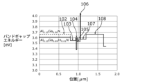
- FIG. FIG. 22 is a graph showing the relationship between the position in the stacking direction of the semiconductor stack 100S of Example E11 and the bandgap energy.
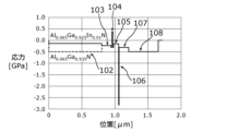
- FIG. 23 is a graph showing the relationship between the stress and the position in the stacking direction of the semiconductor stack 100S of Example E11. The stress shown in FIG.
- FIG. 23 is the stress on the substrate 101, a positive stress value means that the stress is compressive, and a negative stress value means that the stress is tensile. means that FIG. 23 also shows the stress when the N-type cladding layer 102 is made of Al 0.065 Ga 0.935 N as in Example E02 by dotted lines.
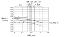
- FIG. 24 is a graph showing the relationship between the position in the stacking direction of the semiconductor stack 100S of Example E11 and the integrated stress.
- the integrated stress means a value obtained by integrating the stress at each position in the stacking direction of the semiconductor stack 100S upward in the stacking direction from the interface between the N-type cladding layer 102 and the substrate 101 in the semiconductor stack 100S. .
- the integrated stress means a value obtained by integrating the stress shown in FIG. 23 from position zero to each position in the stacking direction.
- FIG. 24 also shows the integral stress in the case where the N-type cladding layer 102 is made of Al 0.065 Ga 0.935 N, as in Example E02, by dotted lines.
- Example E11 the bandgap energy of the N-type cladding layer 102 can be reduced more than in Example E02. That is, in Example E11, the refractive index of the N-type cladding layer 102 can be increased more than in Example E02. Therefore, it is possible to prevent the peak position of the light intensity distribution in the lamination direction from being excessively biased in the direction from the active layer 104 toward the P-type cladding layer 108 .
- Example E11 the tensile stress (strain) in the N-type cladding layer 102 can be reduced more than in Example E02.
- the integrated stress is ⁇ 725.8 Pa ⁇ m, and the warp of the wafer (see FIG. 21 ) becomes 553.6 ⁇ m.
- the semiconductor laminate 100S of Example E11 is laminated on a GaN substrate having a size of 5 cm square and a thickness of 85 ⁇ m, the integrated stress is ⁇ 436.4 Pa ⁇ m, and the warpage of the wafer is 335.0 Pa ⁇ m. 0 ⁇ m.
- the warp of the wafer can be reduced, the breakage of the wafer and the occurrence of cracks in the wafer can be suppressed.
- the optical confinement factor was 4.95%
- the effective refractive index difference ⁇ N was 9.29 ⁇ 10 ⁇ 3
- the waveguide loss was 4.23 cm ⁇ 1
- the vertical light distribution peak A nitride-based semiconductor light-emitting device 100 with a position of 8.2 nm can be realized.
- Example E12 Example E12 will be described.
- Example E12 is different from Example E05 in that the N-type cladding layer 102 contains Al and In, and is otherwise identical to Example E05.
- the composition of the N-type cladding layer 102 is Al0.10Ga0.89In0.01N . Effects of the N-type cladding layer 102 containing Al and In in this manner will be described with reference to FIGS. 25 to 27.
- FIG. FIG. 25 is a graph showing the relationship between the position in the stacking direction of the semiconductor stack 100S of Example E12 and the bandgap energy.
- FIG. 26 is a graph showing the relationship between the stress and the position in the stacking direction of the semiconductor stack 100S of Example E12. Note that FIG.
- FIG. 26 also shows the stress in the case where the N-type cladding layer 102 is made of Al 0.10 Ga 0.90 N, as in Example E05, by a dotted line.
- FIG. 27 is a graph showing the relationship between the position in the stacking direction of the semiconductor stack 100S of Example E12 and the integrated stress. Note that FIG. 27 also shows the integral stress in the case where the N-type cladding layer 102 is made of Al 0.10 Ga 0.90 N, as in Example E05, by dotted lines.
- Example E12 When the semiconductor laminate 100S of Example E12 is laminated on a GaN substrate having a size of 5 cm square and a thickness of 85 ⁇ m, the integrated stress is ⁇ 835.5 Pa ⁇ m, and the warp of the wafer (see FIG. 21) is , 639.4 ⁇ m.
- the semiconductor laminate 100S in which the N-type cladding layer 102 is made of Al 0.10 Ga 0.90 N as in Example E05 is laminated on a GaN substrate having a size of 5 cm square and a thickness of 85 ⁇ m.
- the integrated stress is ⁇ 1126.4 Pa ⁇ m
- the warp of the wafer is 858.9 ⁇ m.
- FIGS. 25 to 27 since the N-type cladding layer 102 contains Al and In, the same effect as in Example E11 can be obtained in Example E12.
- the optical confinement factor is 5.87%
- the effective refractive index difference ⁇ N is 10.9 ⁇ 10 ⁇ 3
- the waveguide loss is 3.5 cm ⁇ 1
- the vertical light distribution peak A nitride-based semiconductor light-emitting device 100 with a position of 11.0 nm can be realized.
- Example E13 will be described.
- Example E13 differs from Example E02 in that the well layer 104b contains Al and In, and is the same as Example E02 in other respects.
- the composition of the well layer 104b is Al0.071Ga0.889In0.04N .
- the bandgap energy In the nitride-based semiconductor light-emitting device 100, in order to emit light of 375 nm or more and 380 nm or less, the bandgap energy must be equal to or higher than the bandgap energy of In 0.01 Ga 0.99 N and equal to or lower than the bandgap energy of GaN. need to use a well layer 104b having a The composition of well layer 104b will be described below with reference to FIG.
- FIG. 28 is a graph for explaining the composition required for the well layer 104b of Example E13.
- the horizontal axis of FIG. 28 indicates the In composition ratio y, and the vertical axis indicates the Al composition ratio x.
- the bandgap energy of the well layer 104b is equal to or higher than the bandgap energy of In 0.01 Ga 0.99 N and equal to or lower than the bandgap energy of GaN.
- the following formula (9) should be satisfied.
- the Al composition ratio x and the In composition ratio y of the well layer 104b are values corresponding to the region between the solid line and the broken line shown in FIG. 28, light of 375 nm or more and 380 nm or less can be emitted.
- FIG. 29 is a graph showing the relationship between the In composition ratio of the well layer 104b and the lattice mismatch with respect to GaN.
- In 0.01 Ga 0.99 N has a compressive lattice mismatch of 0.11 % with respect to GaN.
- the compressive lattice mismatch that occurs in the well layer 104b is at most 0.11%.
- the composition of the well layer 104b is Al x Ga 1-x-y In y N having an Al composition ratio x and an In composition ratio y satisfying the formula (9) will be described.
- the compressive lattice mismatch occurring in the well layer 104b is 0.23% or more and 0.28% or less, as shown in FIG.
- the well layer 104b containing Al and In can increase the compressive lattice mismatch that occurs in the well layer 104b. Therefore, tensile strain in the active layer 104 and its peripheral region can be reduced. For example, if the In composition ratio in the well layer 104b is 0.06, the compressive lattice mismatch of the well layer 104b can be increased to 0.34% or more and 0.38% or less, as shown in FIG. Therefore, the tensile strain in the active layer 104 and its peripheral region can be further reduced.
- the optical confinement factor was 5.69%
- the effective refractive index difference ⁇ N was 18.79 ⁇ 10 ⁇ 3
- the waveguide loss was 4.96 cm ⁇ 1
- the vertical light distribution peak A nitride-based semiconductor light-emitting device 100 with a position of 12.84 nm can be realized.
- Example E14 will be described.
- Example E14 differs from Example E01 in the configuration of the N-side guide layer 103, but is the same in other configurations.
- the configuration of the semiconductor laminate 100S of Example E14 will be described below with reference to FIG.
- FIG. 30 is a graph schematically showing the bandgap energy distribution in the stacking direction of the semiconductor stack 100S of Example E14.
- the N-side guide layer 103 of Example 14 includes a first N-side guide layer 103a and a second N-side guide layer 103b arranged above the first N-side guide layer 103a. have.
- the bandgap energy of the first N-side guide layer 103a is greater than the bandgap energy of the second N-side guide layer 103b.
- the Al composition ratio Xng1 of the first N-side guide layer 103a is larger than the Al composition ratio Xng of the second N-side guide layer 103b.
- the first N-side guide layer 103a is an undoped Al 0.04 Ga 0.96 N layer with a thickness of 90 nm.
- the Al composition ratio Xng1 of the first N-side guide layer 103a is 4.0%.
- the second N-side guide layer 103b is an undoped Al 0.02 Ga 0.98 N layer with a thickness of 90 nm. That is, the Al composition ratio Xng2 of the second N-side guide layer 103b is 2.0%.
- Example E14 the average Al composition ratio Xng of the N-side guide layer 103 is 3.0%, satisfying Xpg1 ⁇ Xng ⁇ Xpg2.
- the average Al composition ratio of the N-side guide layer 103 is the average Al composition ratio considering the Al composition ratio distribution in the first N-side guide layer 103a and the second N-side guide layer 103b. More specifically, the average Al composition ratio of the N-side guide layer 103 means the size of the Al composition ratio at a certain position including the first N-side guide layer 103a and the second N-side guide layer 103b.
- the average refractive index of the first P-side guide layer 105 is larger than the average refractive index of the N-side guide layer 103, and the N-side guide layer 103 is larger than the average refractive index of the second P-side guide layer 107 .
- the average refractive index of the N-side guide layer 103 means the average refractive index considering the refractive index distribution in the first N-side guide layer 103a and the second N-side guide layer 103b. More specifically, the average refractive index of the N-side guide layer 103 means the magnitude of the refractive index at a certain position including the first N-side guide layer 103a and the second N-side guide layer 103b.
- the semiconductor stacked body 100S of Comparative Example C30 is an example of the semiconductor stacked body 100S according to Embodiment 1, and the bandgap energy of the first N-side guide layer 103a is higher than the bandgap energy of the second N-side guide layer 103b. It is different from Example E14 in a small point, and is identical in other configurations.
- the first N-side guide layer 103a of Comparative Example C30 is an undoped Al 0.02 Ga 0.98 N layer with a thickness of 90 nm
- the second N-side guide layer 103b is an undoped Al 0.04 Ga with a thickness of 90 nm. 0.96 N layers.
- the average Al composition of the N-side guide layer 103 was the same as in Examples E01 and E14, and the first N-side guide layer 103 in the region far from the active layer 104 of the N-side guide layer 103
- the Al composition ratio of the layer 103a is 2%
- the Al composition ratio of the second N-side guide layer 103b which is a region of the N-side guide layer 103 near the active layer 104, is 4%.
- the optical confinement factor was 5.1%
- the effective refractive index difference ⁇ N was 16.8 ⁇ 10 ⁇ 3
- the waveguide loss was 6.8 ⁇ 10 ⁇ 3 .
- 1 cm ⁇ 1 and the vertical light distribution peak position is 11.6 nm.
- the Al composition ratio (Xng2) of the region of the N-side guide layer 103 near the active layer 104 is decreased as in Example E14, the refractive index of the region of the N-side guide layer 103 near the active layer 104 becomes N It is higher than the refractive index of the region of the side guide layer 103 far from the active layer 104 . Therefore, the proportion of light positioned in the undoped first N-side guide layer 103a, second N-side guide layer 103b, and first P-side guide layer 105 near the active layer 104 increases.
- the waveguide loss is further reduced as compared with the nitride-based semiconductor light-emitting device 100 including the semiconductor laminate 100S of Example E01.
- the light confinement factor in the active layer 104 is further increased.
- the optical confinement factor was 6.2%
- the effective refractive index difference ⁇ N was 17.4 ⁇ 10 ⁇ 3
- the waveguide loss was 3.6 cm ⁇ 1 .
- the nitride-based semiconductor light emitting device 100 having a vertical light distribution peak position of 5.6 nm can be realized.
- the effective refractive index difference ⁇ N of 10 ⁇ 10 ⁇ 3 or more can be realized while the vertical light distribution peak position is located in the well layer 104b region of the active layer 104. It is possible to reduce the wave path loss and increase the optical confinement factor.
- Example E15 will be described.
- Example E15 differs from Example E01 in the configuration of the N-side guide layer 103, but is the same in other configurations.
- the configuration of the semiconductor laminate 100S of Example E15 will be described below with reference to FIG.
- FIG. 31 is a graph schematically showing the bandgap energy distribution in the stacking direction of the semiconductor stack 100S of Example E15.
- the N-side guide layer 103 of Example E15 differs from the N-side guide layer 103 of Example E01 in that it includes a region in which the Al composition ratio monotonically increases as the distance from the active layer 104 increases. differ.
- the N-side guide layer 103 includes a bandgap gradient region in which the bandgap energy increases with increasing distance from the active layer 104 .
- the Al composition ratios Xng near and far from the active layer 104 of the N-side guide layer 103 are 2.0% and 4.0%, respectively.
- Example E15 the average Al composition ratio Xng of the N-side guide layer 103 is 3.0%, satisfying Xpg1 ⁇ Xng ⁇ Xpg2.
- the average refractive index of the first P-side guide layer 105 is larger than the average refractive index of the N-side guide layer 103, and the N-side guide layer 103 is larger than the average refractive index of the second P-side guide layer 107 .
- the refractive index of the region of the N-side guide layer 103 near the active layer 104 becomes It will be higher than the refractive index of the region far from 104 . Therefore, the proportion of light positioned in the undoped N-side guide layer 103 and the first P-side guide layer 105 near the active layer 104 increases. Therefore, in the nitride-based semiconductor light-emitting device 100 including the semiconductor laminate 100S of Example E15, the waveguide loss is further reduced as compared with the nitride-based semiconductor light-emitting device 100 including the semiconductor laminate 100S of Example E01. In addition, the light confinement factor in the active layer 104 is further increased.
- the optical confinement factor was 5.9%
- the effective refractive index difference ⁇ N was 17.4 ⁇ 10 ⁇ 3
- the waveguide loss was 4.1 cm ⁇ 1 .
- the nitride-based semiconductor light emitting device 100 having a vertical light distribution peak position of 6.5 nm can be realized.
- the effective refractive index difference ⁇ N of 10 ⁇ 10 ⁇ 3 or more can be realized while the vertical light distribution peak position is located in the well layer 104b region of the active layer 104. It is possible to reduce the wave path loss and increase the optical confinement factor.
- FIG. 32 is a schematic cross-sectional view showing the overall configuration of a nitride-based semiconductor light-emitting device 200 according to this embodiment.
- a nitride-based semiconductor light-emitting device 200 includes a substrate 101, a semiconductor laminate 200S, a current blocking layer 110, a P-side electrode 111, and an N-side electrode 112.
- the semiconductor stacked body 200S according to the present embodiment differs from the semiconductor stacked body 100S according to the first embodiment in that it includes a buffer layer 221, but is the same as the semiconductor stacked body 100S according to the first embodiment.
- the buffer layer 221 is arranged between the substrate 101 and the N-type cladding layer 102 and is an example of a first buffer layer made of InGaN.
- the buffer layer 221 is an N-type In 0.05 Ga 0.95 N layer with a thickness of 150 nm doped with Si at a concentration of 5 ⁇ 10 17 cm ⁇ 3 .
- the nitride-based semiconductor light emitting device 200 includes the buffer layer 221, compressive strain can be applied to the semiconductor stacked body 200S. As a result, the tensile strain of the semiconductor laminate 200S can be reduced, so that when the semiconductor laminate 200S is laminated on the GaN wafer and processed, cracks in the wafer can be suppressed.
- the semiconductor laminate 200S is laminated on a GaN substrate having a size of 5 cm square and a thickness of 85 ⁇ m, the integrated stress is ⁇ 173.4 Pa ⁇ m, and the warpage of the wafer is 138.1 ⁇ m.
- the refractive index of the substrate 101 is higher than the effective refractive index of the semiconductor laminate 200S for the waveguide mode, so the light diffuses over the entire substrate 101. do.
- the optical confinement factor of the waveguide mode in the active layer 104 is lowered and the waveguide loss is increased, so that the oscillation threshold current value is increased.
- the operating carrier density in the well layer 104b increases, the refractive index of the current injection region in the well layer 104b decreases, the effective refractive index difference ⁇ N decreases, and light propagating in the waveguide including the ridge 108R is guided.
- the wave mechanism becomes a refractive index anti-guiding mechanism.
- the horizontal transverse mode becomes unstable, and kinks tend to occur in the current-optical output characteristics.
- the buffer layer 221 made of InGaN having a bandgap energy smaller than the energy corresponding to ultraviolet light, the buffer layer 221 absorbs light. Therefore, light reaching the substrate 101 can be suppressed.
- the optical confinement factor is 5.69%
- the effective refractive index difference ⁇ N is 18.79 ⁇ 10 ⁇ 3
- the waveguide loss is 4.96 cm ⁇ 1
- the vertical light distribution A nitride-based semiconductor light-emitting device 100 having a peak position of 12.84 nm can be realized.
- FIG. 33 is a schematic cross-sectional view showing the overall configuration of a nitride-based semiconductor light-emitting device 300 according to this embodiment.
- a nitride-based semiconductor light-emitting device 300 includes a substrate 101, a semiconductor laminate 300S, a current blocking layer 110, a P-side electrode 111, and an N-side electrode 112.
- a semiconductor stacked body 300S according to the present embodiment differs from the semiconductor stacked body 200S according to the second embodiment in that a buffer layer 321 is provided, and is the same in other respects.
- the buffer layer 321 is arranged between the substrate 101 and the N-type cladding layer 102 and is an example of a second buffer layer made of AlGaN. In this embodiment, buffer layer 321 is positioned between substrate 101 and buffer layer 221 .
- the buffer layer 321 is an N-type Al 0.007 Ga 0.993 N layer with a thickness of 1000 nm doped with Si at a concentration of 5 ⁇ 10 17 cm ⁇ 3 .
- the nitride-based semiconductor light-emitting device 300 according to the present embodiment also has the same effects as the nitride-based semiconductor light-emitting device 200 according to the second embodiment.
- the semiconductor laminate 300S is laminated on a GaN substrate having a size of 5 cm square and a thickness of 85 ⁇ m
- the integral stress is ⁇ 227.5 Pa ⁇ m
- the warp of the wafer is 173.8 ⁇ m.
- the optical confinement factor is 5.69%
- the effective refractive index difference ⁇ N is 18.79 ⁇ 10 ⁇ 3
- the waveguide loss is 4.96 cm ⁇ 1
- the vertical light distribution A nitride-based semiconductor light-emitting device 100 having a peak position of 12.84 nm can be realized.
- the nitride-based semiconductor light-emitting device is a semiconductor laser device, but the nitride-based semiconductor light-emitting device is not limited to a semiconductor laser device.
- the nitride-based semiconductor light emitting device may be a superluminescent diode.
- the reflectance of the end surface of the semiconductor laminate included in the nitride-based semiconductor light-emitting device with respect to the emitted light from the semiconductor laminate may be 0.1% or less.
- Such a reflectance can be realized, for example, by forming an antireflection film made of a dielectric multilayer film or the like on the end face.
- the guided light reflected by the front end face is coupled again with the waveguide to form a guided light component.
- the P-type clad layer 108 is a layer with a uniform Al composition ratio, but the configuration of the P-type clad layer 108 is not limited to this.
- the P-type cladding layer 108 may have a superlattice structure in which each of a plurality of AlGaN layers and each of a plurality of GaN layers are alternately laminated.
- each buffer layer according to the second and third embodiments may be applied to each example of the nitride-based semiconductor light emitting device 100 according to the first embodiment.
- the nitride-based semiconductor light-emitting device of the present disclosure can be applied, for example, as a high-output and high-efficiency light source to light sources for exposure apparatuses and processing machines.
Landscapes
- Physics & Mathematics (AREA)
- Condensed Matter Physics & Semiconductors (AREA)
- General Physics & Mathematics (AREA)
- Electromagnetism (AREA)
- Optics & Photonics (AREA)
- Geometry (AREA)
- Semiconductor Lasers (AREA)
Abstract
L'invention concerne un élément électroluminescent à semi-conducteur à base de nitrure (100) comprenant : une couche de placage de type N (102) ; une couche de guidage côté N (103) disposée au-dessus de la couche de placage de type N (102) ; une couche active (104) disposée au-dessus de la couche de guidage côté N (103) ; une première couche de guidage côté P (105) disposée au-dessus de la couche active (104) ; une couche barrière électronique (106) disposée au-dessus de la première couche de guidage côté P (105) ; une seconde couche de guidage côté P (107) disposée au-dessus de la couche barrière électronique (106) ; et une couche de placage de type P (108) disposée au-dessus de la seconde couche de guidage côté P (107). L'énergie de bande interdite moyenne de la seconde couche de guidage côté P (107) est supérieure à l'énergie de bande interdite moyenne de la première couche de guidage côté P (105), et l'énergie de bande interdite moyenne de la couche de placage de type P (108) est inférieure à l'énergie de bande interdite moyenne de la couche barrière électronique (106).
Applications Claiming Priority (2)
| Application Number | Priority Date | Filing Date | Title |
|---|---|---|---|
| JP2022-020107 | 2022-02-14 | ||
| JP2022020107A JP2023117509A (ja) | 2022-02-14 | 2022-02-14 | 窒化物系半導体発光素子 |
Publications (1)
| Publication Number | Publication Date |
|---|---|
| WO2023153330A1 true WO2023153330A1 (fr) | 2023-08-17 |
Family
ID=87564358
Family Applications (1)
| Application Number | Title | Priority Date | Filing Date |
|---|---|---|---|
| PCT/JP2023/003577 WO2023153330A1 (fr) | 2022-02-14 | 2023-02-03 | Élément électroluminescent à semi-conducteur à base de nitrure |
Country Status (2)
| Country | Link |
|---|---|
| JP (1) | JP2023117509A (fr) |
| WO (1) | WO2023153330A1 (fr) |
Citations (9)
| Publication number | Priority date | Publication date | Assignee | Title |
|---|---|---|---|---|
| JPH11340510A (ja) * | 1998-03-27 | 1999-12-10 | Sharp Corp | 半導体素子及びその製造方法 |
| JP2002335052A (ja) * | 2001-05-10 | 2002-11-22 | Nichia Chem Ind Ltd | 窒化物半導体素子 |
| US20070248135A1 (en) * | 2006-04-19 | 2007-10-25 | Mawst Luke J | Quantum well lasers with strained quantum wells and dilute nitride barriers |
| JP2010109332A (ja) * | 2008-09-30 | 2010-05-13 | Sanyo Electric Co Ltd | 半導体レーザ装置および表示装置 |
| JP2010263163A (ja) * | 2009-05-11 | 2010-11-18 | Sumitomo Electric Ind Ltd | 窒化物半導体発光素子 |
| JP2011146650A (ja) * | 2010-01-18 | 2011-07-28 | Sumitomo Electric Ind Ltd | GaN系半導体発光素子およびその製造方法 |
| JP2013038394A (ja) * | 2011-07-14 | 2013-02-21 | Rohm Co Ltd | 半導体レーザ素子 |
| JP2017073511A (ja) * | 2015-10-09 | 2017-04-13 | 旭化成株式会社 | 半導体発光素子 |
| JP2018517295A (ja) * | 2015-05-19 | 2018-06-28 | イェール ユニバーシティーYale University | 格子整合クラッド層を有する高い閉じ込め係数のiii窒化物端面発光レーザーダイオードに関する方法およびデバイス |
-
2022
- 2022-02-14 JP JP2022020107A patent/JP2023117509A/ja active Pending
-
2023
- 2023-02-03 WO PCT/JP2023/003577 patent/WO2023153330A1/fr unknown
Patent Citations (9)
| Publication number | Priority date | Publication date | Assignee | Title |
|---|---|---|---|---|
| JPH11340510A (ja) * | 1998-03-27 | 1999-12-10 | Sharp Corp | 半導体素子及びその製造方法 |
| JP2002335052A (ja) * | 2001-05-10 | 2002-11-22 | Nichia Chem Ind Ltd | 窒化物半導体素子 |
| US20070248135A1 (en) * | 2006-04-19 | 2007-10-25 | Mawst Luke J | Quantum well lasers with strained quantum wells and dilute nitride barriers |
| JP2010109332A (ja) * | 2008-09-30 | 2010-05-13 | Sanyo Electric Co Ltd | 半導体レーザ装置および表示装置 |
| JP2010263163A (ja) * | 2009-05-11 | 2010-11-18 | Sumitomo Electric Ind Ltd | 窒化物半導体発光素子 |
| JP2011146650A (ja) * | 2010-01-18 | 2011-07-28 | Sumitomo Electric Ind Ltd | GaN系半導体発光素子およびその製造方法 |
| JP2013038394A (ja) * | 2011-07-14 | 2013-02-21 | Rohm Co Ltd | 半導体レーザ素子 |
| JP2018517295A (ja) * | 2015-05-19 | 2018-06-28 | イェール ユニバーシティーYale University | 格子整合クラッド層を有する高い閉じ込め係数のiii窒化物端面発光レーザーダイオードに関する方法およびデバイス |
| JP2017073511A (ja) * | 2015-10-09 | 2017-04-13 | 旭化成株式会社 | 半導体発光素子 |
Also Published As
| Publication number | Publication date |
|---|---|
| JP2023117509A (ja) | 2023-08-24 |
Similar Documents
| Publication | Publication Date | Title |
|---|---|---|
| US20070002914A1 (en) | Semiconductor laser diode having an asymmetric optical waveguide layer | |
| US8731016B2 (en) | Nitride semiconductor light emitting device | |
| JP7447028B2 (ja) | 半導体発光素子 | |
| JP5170954B2 (ja) | 半導体レーザ装置 | |
| US11296485B2 (en) | Semiconductor laser element and method for manufacturing the same | |
| US11710941B2 (en) | Semiconductor laser element | |
| JPWO2008010374A1 (ja) | 半導体レーザ装置 | |
| WO2019187583A1 (fr) | Élément électroluminescent à semi-conducteur | |
| US7289546B1 (en) | Semiconductor laser having an improved stacked structure | |
| WO2023153330A1 (fr) | Élément électroluminescent à semi-conducteur à base de nitrure | |
| JP4660333B2 (ja) | 窒化物系半導体レーザ素子 | |
| WO2023243518A1 (fr) | Dispositif électroluminescent à semi-conducteur à base de nitrure | |
| WO2022202448A1 (fr) | Élément électroluminescent à semi-conducteur au nitrure | |
| US20230387352A1 (en) | Nitride semiconductor light-emitting element | |
| US10218152B1 (en) | Semiconductor laser diode with low threshold current | |
| WO2024070351A1 (fr) | Dispositif électroluminescent à semi-conducteur à base de nitrure | |
| WO2023153035A1 (fr) | Élément électroluminescent à semi-conducteur au nitrure | |
| WO2023026858A1 (fr) | Élément électroluminescent à semi-conducteur au nitrure | |
| WO2023281902A1 (fr) | Élément émetteur de lumière à semi-conducteur au nitrure | |
| US11509117B2 (en) | Light emitting element | |
| WO2023238655A1 (fr) | Élément électroluminescent à semi-conducteur | |
| WO2024084898A1 (fr) | Élément électroluminescent à cavité verticale | |
| US20230387662A1 (en) | Semiconductor laser element | |
| CN109787087B (zh) | 氮化物半导体激光元件 | |
| JP2024075517A (ja) | 窒化物系半導体発光素子 |
Legal Events
| Date | Code | Title | Description |
|---|---|---|---|
| 121 | Ep: the epo has been informed by wipo that ep was designated in this application |
Ref document number: 23752795 Country of ref document: EP Kind code of ref document: A1 |