WO2023153035A1 - Élément électroluminescent à semi-conducteur au nitrure - Google Patents
Élément électroluminescent à semi-conducteur au nitrure Download PDFInfo
- Publication number
- WO2023153035A1 WO2023153035A1 PCT/JP2022/041910 JP2022041910W WO2023153035A1 WO 2023153035 A1 WO2023153035 A1 WO 2023153035A1 JP 2022041910 W JP2022041910 W JP 2022041910W WO 2023153035 A1 WO2023153035 A1 WO 2023153035A1
- Authority
- WO
- WIPO (PCT)
- Prior art keywords
- layer
- nitride
- side guide
- emitting device
- guide layer
- Prior art date
Links
- 239000004065 semiconductor Substances 0.000 title claims abstract description 480
- 150000004767 nitrides Chemical class 0.000 title claims abstract description 260
- 230000004888 barrier function Effects 0.000 claims abstract description 160
- 239000000758 substrate Substances 0.000 claims abstract description 96
- 229910002704 AlGaN Inorganic materials 0.000 claims abstract description 39
- 238000005253 cladding Methods 0.000 claims description 185
- 239000000203 mixture Substances 0.000 claims description 100
- 230000003287 optical effect Effects 0.000 claims description 30
- 239000010410 layer Substances 0.000 description 1347
- 238000009826 distribution Methods 0.000 description 40
- 230000000903 blocking effect Effects 0.000 description 24
- 239000012535 impurity Substances 0.000 description 21
- 230000004048 modification Effects 0.000 description 14
- 238000012986 modification Methods 0.000 description 14
- 230000000694 effects Effects 0.000 description 9
- 238000000034 method Methods 0.000 description 7
- JMASRVWKEDWRBT-UHFFFAOYSA-N Gallium nitride Chemical compound [Ga]#N JMASRVWKEDWRBT-UHFFFAOYSA-N 0.000 description 5
- 238000009792 diffusion process Methods 0.000 description 5
- 238000002347 injection Methods 0.000 description 5
- 239000007924 injection Substances 0.000 description 5
- 230000031700 light absorption Effects 0.000 description 5
- 238000003475 lamination Methods 0.000 description 4
- 230000010355 oscillation Effects 0.000 description 4
- 239000000470 constituent Substances 0.000 description 3
- 239000013078 crystal Substances 0.000 description 3
- 238000004519 manufacturing process Methods 0.000 description 3
- 238000000206 photolithography Methods 0.000 description 3
- 239000002356 single layer Substances 0.000 description 3
- VYPSYNLAJGMNEJ-UHFFFAOYSA-N Silicium dioxide Chemical compound O=[Si]=O VYPSYNLAJGMNEJ-UHFFFAOYSA-N 0.000 description 2
- 239000000969 carrier Substances 0.000 description 2
- 229910052804 chromium Inorganic materials 0.000 description 2
- 238000005530 etching Methods 0.000 description 2
- 229910052737 gold Inorganic materials 0.000 description 2
- 229910052759 nickel Inorganic materials 0.000 description 2
- 229910052763 palladium Inorganic materials 0.000 description 2
- 229910052697 platinum Inorganic materials 0.000 description 2
- 229910052719 titanium Inorganic materials 0.000 description 2
- UFHFLCQGNIYNRP-UHFFFAOYSA-N Hydrogen Chemical compound [H][H] UFHFLCQGNIYNRP-UHFFFAOYSA-N 0.000 description 1
- 238000004364 calculation method Methods 0.000 description 1
- 238000005229 chemical vapour deposition Methods 0.000 description 1
- 229910052681 coesite Inorganic materials 0.000 description 1
- 229910052906 cristobalite Inorganic materials 0.000 description 1
- 230000006866 deterioration Effects 0.000 description 1
- 238000010586 diagram Methods 0.000 description 1
- 238000005516 engineering process Methods 0.000 description 1
- 229910052739 hydrogen Inorganic materials 0.000 description 1
- 239000001257 hydrogen Substances 0.000 description 1
- 230000004807 localization Effects 0.000 description 1
- 239000000463 material Substances 0.000 description 1
- 239000002184 metal Substances 0.000 description 1
- 229910052751 metal Inorganic materials 0.000 description 1
- 238000005424 photoluminescence Methods 0.000 description 1
- 238000005268 plasma chemical vapour deposition Methods 0.000 description 1
- 239000000377 silicon dioxide Substances 0.000 description 1
- 235000012239 silicon dioxide Nutrition 0.000 description 1
- 229910052682 stishovite Inorganic materials 0.000 description 1
- 229910052905 tridymite Inorganic materials 0.000 description 1
- 238000007740 vapor deposition Methods 0.000 description 1
Images


Classifications
-
- H—ELECTRICITY
- H01—ELECTRIC ELEMENTS
- H01L—SEMICONDUCTOR DEVICES NOT COVERED BY CLASS H10
- H01L33/00—Semiconductor devices having potential barriers specially adapted for light emission; Processes or apparatus specially adapted for the manufacture or treatment thereof or of parts thereof; Details thereof
- H01L33/02—Semiconductor devices having potential barriers specially adapted for light emission; Processes or apparatus specially adapted for the manufacture or treatment thereof or of parts thereof; Details thereof characterised by the semiconductor bodies
- H01L33/26—Materials of the light emitting region
- H01L33/30—Materials of the light emitting region containing only elements of Group III and Group V of the Periodic Table
- H01L33/32—Materials of the light emitting region containing only elements of Group III and Group V of the Periodic Table containing nitrogen
-
- H—ELECTRICITY
- H01—ELECTRIC ELEMENTS
- H01S—DEVICES USING THE PROCESS OF LIGHT AMPLIFICATION BY STIMULATED EMISSION OF RADIATION [LASER] TO AMPLIFY OR GENERATE LIGHT; DEVICES USING STIMULATED EMISSION OF ELECTROMAGNETIC RADIATION IN WAVE RANGES OTHER THAN OPTICAL
- H01S5/00—Semiconductor lasers
- H01S5/30—Structure or shape of the active region; Materials used for the active region
- H01S5/34—Structure or shape of the active region; Materials used for the active region comprising quantum well or superlattice structures, e.g. single quantum well [SQW] lasers, multiple quantum well [MQW] lasers or graded index separate confinement heterostructure [GRINSCH] lasers
- H01S5/343—Structure or shape of the active region; Materials used for the active region comprising quantum well or superlattice structures, e.g. single quantum well [SQW] lasers, multiple quantum well [MQW] lasers or graded index separate confinement heterostructure [GRINSCH] lasers in AIIIBV compounds, e.g. AlGaAs-laser, InP-based laser
Definitions
- the present disclosure relates to a nitride-based semiconductor light-emitting device.
- nitride-based semiconductor light-emitting devices that emit blue light are known, but there is a demand for high-output nitride-based semiconductor light-emitting devices that emit ultraviolet light with a shorter wavelength (for example, Patent Document 1, etc.). reference).
- a nitride-based semiconductor light-emitting device can realize a watt-class ultraviolet laser light source, it can be used as a light source for exposure, a light source for processing, and the like.
- An active layer having a quantum well structure is used as a light-emitting layer of a nitride-based semiconductor light-emitting device that emits ultraviolet light.
- Such active layers include one or more well layers and multiple barrier layers. Since ultraviolet light has a shorter wavelength (that is, higher energy) than visible light, the bandgap energy of the well layer that emits ultraviolet light is greater than the bandgap energy of the well layer that emits visible light. Therefore, in order to secure the quantum effect in the quantum well structure, it is necessary to increase the bandgap energy of the barrier layer.
- the refractive index of the barrier layer becomes smaller, so it is necessary to increase the Al composition ratio of the clad layer in order to make the refractive index of the clad layer smaller than that of the barrier layer.
- the tensile strain in the semiconductor laminate such as the clad layer with respect to the GaN substrate increases.
- the crystallinity of the semiconductor laminate is degraded, and cracks are likely to occur in the semiconductor laminate.
- the present disclosure aims to solve such problems, and aims to provide a nitride-based semiconductor light-emitting device capable of reducing the tensile strain of the semiconductor laminate with respect to the substrate.
- one aspect of the nitride-based semiconductor light-emitting device includes a substrate made of GaN, a first cladding layer made of AlGaN disposed above the substrate, and above the substrate. , the first cladding layer, and a first semiconductor layer disposed between the active layer, the active layer comprising a well layer made of a nitride-based semiconductor and Al made of the average bandgap energy of the first semiconductor layer is smaller than the average bandgap energy of the first cladding layer, and the first semiconductor layer is made of AlGaInN.
- another aspect of the nitride-based semiconductor light-emitting device includes a substrate made of GaN, an N-type cladding layer made of AlGaN disposed above the substrate, and the N-type cladding layer made of AlGaN.
- an N-side semiconductor layer arranged above the type cladding layer and made of a nitride-based semiconductor; an active layer arranged above the N-side semiconductor layer; and an active layer arranged above the active layer and made of the nitride-based semiconductor.
- an average bandgap energy of the N-side semiconductor layer is smaller than an average bandgap energy of the N-type cladding layer, and an average bandgap energy of the P-side semiconductor layer is equal to the P-type
- At least one of the N-side semiconductor layer and the P-side semiconductor layer is made of AlGaInN, which is smaller than the average bandgap energy of the cladding layer.
- a nitride-based semiconductor light-emitting device capable of reducing the tensile strain of the semiconductor laminate with respect to the substrate.
- FIG. 1 is a schematic plan view showing the overall configuration of a nitride-based semiconductor light-emitting device according to Embodiment 1.
- FIG. 2A is a schematic cross-sectional view showing the overall configuration of the nitride-based semiconductor light-emitting device according to Embodiment 1.
- FIG. 2B is a schematic cross-sectional view showing the configuration of an active layer included in the nitride-based semiconductor light-emitting device according to Embodiment 1.
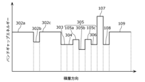
- FIG. FIG. 3 is a graph showing the distribution of the bandgap energy in the stacking direction of the semiconductor stack according to the first embodiment.
- FIG. 4 is a graph showing the relationship between the bandgap energy in the AlxGa1 -xyInyN layer and the bandgap energy in the AlzGa1 -zN layer.
- FIG. 5 is a graph showing the distribution of the bandgap energy in the stacking direction of the semiconductor stack according to the second embodiment.
- FIG. 6 is a graph showing the distribution of the bandgap energy in the stacking direction of the semiconductor stack according to the third embodiment.
- FIG. 7 is a graph showing the distribution of the bandgap energy in the stacking direction of the semiconductor stack according to the fourth embodiment.
- FIG. 8 is a graph showing the distribution of the bandgap energy in the stacking direction of the semiconductor stack according to the fifth embodiment.
- FIG. 9 is a graph showing the distribution of the bandgap energy in the stacking direction of the semiconductor stack according to the sixth embodiment.
- FIG. 10 is a graph showing the distribution of the bandgap energy in the stacking direction of the semiconductor stack according to the seventh embodiment.
- FIG. 11 is a graph showing the distribution of the bandgap energy in the stacking direction of the semiconductor stack according to the eighth embodiment.
- FIG. 12 is a graph showing the distribution of the bandgap energy in the stacking direction of the semiconductor stack according to the ninth embodiment.
- FIG. 13 is a graph showing the distribution of the bandgap energy in the stacking direction of the semiconductor stack according to the tenth embodiment.
- FIG. 10 is a graph showing the distribution of the bandgap energy in the stacking direction of the semiconductor stack according to the seventh embodiment.
- FIG. 11 is a graph showing the distribution of the bandgap energy in the stacking direction of the semiconductor stack according to the eighth embodiment.
- FIG. 12 is a graph showing the distribution of the bandg
- FIG. 14 is a graph showing the distribution of the bandgap energy in the stacking direction of the semiconductor stack according to the eleventh embodiment.
- FIG. 15 is a graph showing the distribution of the bandgap energy in the stacking direction of the semiconductor stack according to the twelfth embodiment.
- FIG. 16 is a graph showing the distribution of the bandgap energy in the stacking direction of the semiconductor stack according to the thirteenth embodiment.
- each figure is a schematic diagram and is not necessarily strictly illustrated. Therefore, the scales and the like are not always the same in each drawing.
- symbol is attached
- the terms “upper” and “lower” do not refer to vertical upper and vertical lower in absolute spatial recognition, but are defined by relative positional relationships based on the stacking order in the stacking structure. used as a term Also, the terms “above” and “below” are used not only when two components are spaced apart from each other and there is another component between the two components, but also when two components are spaced apart from each other. It also applies when they are arranged in contact with each other.
- Embodiment 1 A nitride-based semiconductor light-emitting device according to Embodiment 1 will be described.
- FIGS. 1, 2A and 2B are a schematic plan view and a cross-sectional view, respectively, showing the overall configuration of a nitride-based semiconductor light-emitting device 100 according to this embodiment.
- FIG. 2A shows a cross-section along line II-II of FIG.
- FIG. 2B is a schematic cross-sectional view showing the configuration of the active layer 105 included in the nitride-based semiconductor light emitting device 100 according to this embodiment.
- Each figure shows an X-axis, a Y-axis, and a Z-axis that are orthogonal to each other.
- the X, Y, and Z axes are a right-handed Cartesian coordinate system.
- the stacking direction of the nitride-based semiconductor light emitting device 100 is parallel to the Z-axis direction, and the main emission direction of light (laser light) is parallel to the Y-axis direction.
- the nitride-based semiconductor light-emitting device 100 includes a semiconductor laminate 100S including nitride-based semiconductor layers. Light is emitted from the end face 100F (see FIG. 1).
- the nitride-based semiconductor light-emitting device 100 is a semiconductor laser device having two facets 100F and 100R forming a resonator.
- the end surface 100F is a front end surface that emits laser light
- the end surface 100R is a rear end surface having a higher reflectance than the end surface 100F.
- the nitride-based semiconductor light emitting device 100 has a waveguide formed between the facet 100F and the facet 100R.
- the reflectances of the end faces 100F and 100R are 16% and 95%, respectively.
- the cavity length of nitride-based semiconductor light-emitting device 100 according to the present embodiment (that is, the distance between facet 100F and facet 100R) is about 1200 ⁇ m.
- the nitride-based semiconductor light emitting device 100 emits ultraviolet light having a peak wavelength in the 375 nm band, for example.
- Nitride-based semiconductor light emitting device 100 may emit ultraviolet light having a peak wavelength in a band other than the 375 nm band, or may emit light having a peak wavelength in a wavelength band other than ultraviolet light.
- the nitride-based semiconductor light emitting device 100 includes a substrate 101, a semiconductor laminate 100S, a current blocking layer 111, a P-side electrode 112, and an N-side electrode 113.
- the semiconductor laminate 100S includes an N-type cladding layer 102, a first N-side guide layer 103, a second N-side guide layer 104, an active layer 105, a first P-side guide layer 106, and an electron barrier layer 107. , a second P-side guide layer 108 , a P-type cladding layer 109 and a contact layer 110 .
- the substrate 101 is a plate-like member that serves as a base for the nitride-based semiconductor light emitting device 100 .
- the substrate 101 is arranged below the N-type cladding layer 102 and is made of N-type GaN. More specifically, substrate 101 is a GaN substrate doped with Si at a concentration of 1 ⁇ 10 18 cm ⁇ 3 .
- the N-type clad layer 102 is an example of a first clad layer arranged above the substrate 101 and made of AlGaN.
- the clad layer is a layer capable of approximating the variation of the light intensity distribution in the layer with respect to the lamination direction by an exponential function.
- the conductivity type of the N-type cladding layer 102 is N-type.
- the N-type cladding layer 102 has a lower refractive index and a higher average bandgap energy than the active layer 105 .
- the N-type cladding layer 102 is an N-type Al 0.065 Ga 0.935 N layer with a thickness of 800 nm doped with Si at a concentration of 5 ⁇ 10 17 cm ⁇ 3 .
- the average bandgap energy of a layer means the magnitude of the bandgap energy at a certain position in the stacking direction of the layer, from the position of the interface on the substrate side in the stacking direction of the layer to the substrate. It is the value of the bandgap energy integrated in the stacking direction up to the position of the interface on the far side and divided by the layer thickness (the distance between the interface on the substrate side and the interface on the far side from the substrate).
- the average refractive index of a layer is the magnitude of the refractive index at a certain position in the stacking direction of that layer, from the position of the interface on the side of the substrate in the stacking direction of that layer to the position of the interface on the far side from the substrate in the stacking direction. , and divided by the film thickness of the layer (the distance between the interface on the substrate side and the interface on the far side from the substrate).
- the average Al composition ratio of a layer means the magnitude of the Al composition ratio at a certain position in the lamination direction of the layer, from the position of the interface on the substrate side in the lamination direction of the layer to the position of the interface on the far side from the substrate. It is the value of the Al composition ratio integrated in the stacking direction and divided by the film thickness of the layer (the distance between the interface on the substrate side and the interface on the far side from the substrate).
- the average impurity concentration of a layer is the magnitude of the impurity concentration at a certain position in the stacking direction of that layer, from the position of the interface on the side of the substrate in the stacking direction of that layer to the position of the interface on the far side from the substrate in the stacking direction. , and divided by the layer thickness (the distance between the interface on the substrate side and the interface on the far side from the substrate).
- An impurity means an impurity doped to obtain an N-type conductivity in an N-type semiconductor layer, and an impurity doped to obtain a P-type conductivity in a P-type semiconductor layer.
- the first N-side guide layer 103 is an example of a first guide layer, which is an optical guide layer arranged between the N-type cladding layer 102 and the active layer 105, and is made of a nitride-based semiconductor.
- the light guide layer is a layer capable of approximating the mode of change in light intensity distribution in the layer with respect to the lamination direction by a trigonometric function.
- the first N-side guide layer 103 has a higher refractive index and a lower bandgap energy than the N-type clad layer 102 .
- the average bandgap energy of the first N-side guide layer 103 is greater than or equal to the average bandgap energy of the second N-side guide layer 104 .
- the first N-side guide layer 103 contains Al. Also, the first N-side guide layer 103 is an N-type nitride semiconductor layer. In other words, the average impurity concentration of the first N-side guide layer 103 is 1 ⁇ 10 17 cm ⁇ 3 or higher. In this embodiment, the first N-side guide layer 103 is arranged between the N-type cladding layer 102 and the second N-side guide layer 104, and is a film doped with Si at a concentration of 5 ⁇ 10 17 cm ⁇ 3 . It is an N-type Al 0.03 Ga 0.97 N layer with a thickness of 70 nm.
- the second N-side guide layer 104 is arranged above the N-type cladding layer 102 and is an example of an N-side semiconductor layer made of a nitride-based semiconductor.
- the second N-side guide layer 104 is arranged between the N-type cladding layer 102 and the active layer 105, and is also an example of the first semiconductor layer made of AlGaInN.
- the second N-side guide layer 104 is an optical guide layer.
- the average bandgap energy of the second N-side guide layer 104 is smaller than the average bandgap energy of the N-type cladding layer 102 .
- the second N-side guide layer 104 is an undoped AlGaInN layer.
- the average impurity concentration of the second N-side guide layer 104 is less than 1 ⁇ 10 17 cm ⁇ 3 .
- the second N-side guide layer 104 is undoped Al 0.05 Ga 0.94 In 0.01 with a thickness of 70 nm, which is arranged between the first N-side guide layer 103 and the active layer 105 . N layer.
- the active layer 105 is a light emitting layer arranged above the substrate 101 .
- the active layer 105 is arranged above the second N-side guide layer 104 .
- the active layer 105 has a quantum well structure and emits ultraviolet light.
- the active layer 105 is a single layer having a well layer 105b made of a nitride-based semiconductor and two barrier layers 105a and 105c made of a nitride-based semiconductor containing Al. It is a quantum well structure.
- a well layer 105b is disposed between two barrier layers 105a and 105c.
- the configuration of the active layer 105 is not limited to this.
- active layer 105 may have a multiple quantum well structure.
- the active layer 105 may have three or more barrier layers and two or more well layers.
- Each of the barrier layers 105a and 105c is a nitride-based semiconductor layer arranged above the first N-side guide layer 103 and functioning as a barrier for the quantum well structure.
- the barrier layer 105c is arranged above the barrier layer 105a.
- the bandgap energy of each of the barrier layers 105a and 105c is equal to the bandgap energy of the well layer 105b, the average bandgap energy of the first P-side guide layer 106, and the average bandgap energy of the first N-side guide layer 103. It is larger than the average bandgap energy and smaller than the average bandgap energy of the electron barrier layer 107 .
- Each of the barrier layers 105a and 105c is an undoped Al 0.07 Ga 0.92 In 0.01 N layer with a thickness of 10 nm. , the average bandgap energy, the Al composition ratio, and the In composition ratio of the barrier layer 105c.
- the well layer 105b is a nitride-based semiconductor layer arranged above the barrier layer 105a and functioning as a well of a quantum well structure.
- the well layer 105b is an undoped In 0.01 Ga 0.99 N layer with a thickness of 17.5 nm.
- the first P-side guide layer 106 is arranged above the active layer 105 and is an example of a P-side semiconductor layer made of a nitride-based semiconductor.
- the first P-side guide layer 106 is arranged between the P-type cladding layer 109 and the active layer 105, and is also an example of the first semiconductor layer made of AlGaInN. That is, in the nitride-based semiconductor light emitting device 100, both the second N-side guide layer 104 (that is, N-side semiconductor layer) and the first P-side guide layer 106 (that is, P-side semiconductor layer) are made of AlGaInN.
- the first P-side guide layer 106 is a light guide layer.
- the average bandgap energy, Al composition ratio, and In composition ratio of the first P-side guide layer 106 are equal to the average bandgap energy, Al composition ratio, and In composition ratio of the second N-side guide layer 104, respectively.
- the average bandgap energy of the first P-side guide layer 106 is smaller than the average bandgap energy of the P-type cladding layer 109 .
- the first P-side guide layer 106 is an undoped AlGaInN layer. In other words, the average impurity concentration of the first P-side guide layer 106 is less than 1 ⁇ 10 18 cm ⁇ 3 .
- the first P-side guide layer 106 is an undoped Al 0.05 Ga 0.94 In 0.01 N layer with a thickness of 72 nm.
- the electron barrier layer 107 is a nitride semiconductor layer arranged between the first P-side guide layer 106 and the P-type cladding layer 109 .
- the bandgap energy of the electron barrier layer 107 is greater than the bandgap energy of the barrier layer 105c. This can suppress leakage of electrons from the active layer 105 to the P-type cladding layer 109 .
- the bandgap energy of the electron barrier layer 107 is greater than the bandgap energy of the P-type cladding layer 109 .
- the electron barrier layer 107 is a 5 nm thick P-type Al 0.30 Ga 0.70 N layer doped with Mg at a concentration of 1 ⁇ 10 19 cm ⁇ 3 .
- the second P-side guide layer 108 is an example of a first guide layer, which is an optical guide layer arranged between the P-type cladding layer 109 and the active layer 105, and is made of a nitride-based semiconductor.
- the second P-side guide layer 108 is also an example of a second guide layer arranged between the electron barrier layer 107 and the P-type cladding layer 109 .
- the average bandgap energy and Al composition ratio of the second P-side guide layer 108 are equal to the average bandgap energy and Al composition ratio of the first N-side guide layer 103, respectively.
- the second P-side guide layer 108 has a higher refractive index and a lower bandgap energy than the P-type cladding layer 109 .
- the average bandgap energy of the second P-side guide layer 108 is greater than or equal to the average bandgap energy of the first P-side guide layer 106 .
- the second P-side guide layer 108 contains Al.
- the second P-side guide layer 108 is a P-type nitride semiconductor layer.
- the average impurity concentration of the second P-side guide layer 108 is 1 ⁇ 10 18 cm ⁇ 3 or more.
- the second P-side guide layer 108 is disposed between the electron barrier layer 107 and the P-type cladding layer 109, and is doped with Mg at a concentration of 1 ⁇ 10 18 cm ⁇ 3 and has a thickness of 148 nm. It is a P-type Al 0.03 Ga 0.97 N layer.
- the P-type clad layer 109 is an example of a first clad layer arranged above the substrate 101 and made of AlGaN.
- the conductivity type of the P-type cladding layer 109 is P-type.
- the P-type cladding layer 109 is arranged above the first P-side guide layer 106 .
- the P-type cladding layer 109 has a smaller refractive index and a larger average bandgap energy than the active layer 105 .
- the average bandgap energy of the P-type cladding layer 109 is smaller than the average bandgap energy of the electron barrier layer 107 .
- the average bandgap energy and Al composition ratio of the P-type clad layer 109 are equal to the average bandgap energy and Al composition ratio of the N-type clad layer 102, respectively.
- the P-type clad layer 109 is doped with Mg as an impurity.
- the impurity concentration at the end portion of the P-type cladding layer 109 closer to the active layer 105 is lower than the impurity concentration at the end portion farther from the active layer 105 .
- the P-type cladding layer 109 is an AlGaN layer with a thickness of 450 nm, and is placed on the side closer to the active layer 105 and is doped with Mg at a concentration of 2 ⁇ 10 18 cm ⁇ 3 with a thickness of 150 nm.
- a ridge 109R is formed in the P-type cladding layer 109. Also, the P-type cladding layer 109 is formed with two grooves 109T arranged along the ridge 109R and extending in the Y-axis direction. In this embodiment, the ridge width W is approximately 30 ⁇ m.
- the contact layer 110 is a nitride-based semiconductor layer arranged above the P-type cladding layer 109 and in ohmic contact with the P-side electrode 112 .
- the contact layer 110 is a P-type GaN layer with a thickness of 60 nm.
- the contact layer 110 is doped with Mg at a concentration of 1 ⁇ 10 20 cm ⁇ 3 as an impurity.
- the current blocking layer 111 is arranged above the P-type cladding layer 109 and is an insulating layer having transparency to light from the active layer 105 .
- the current blocking layer 111 is arranged in a region of the top surfaces of the P-type cladding layer 109 and the contact layer 110 other than the top surface of the ridge 109R.
- the current blocking layer 111 may also be arranged on a partial region of the upper surface of the ridge 109R.
- current blocking layer 111 may be disposed in the edge region of the top surface of ridge 109R.
- the current blocking layer 111 is a SiO2 layer.
- the P-side electrode 112 is a conductive layer arranged above the contact layer 110 .
- the P-side electrode 112 is arranged above the contact layer 110 and the current blocking layer 111 .
- the P-side electrode 112 is, for example, a single layer film or a multilayer film made of at least one of Cr, Ti, Ni, Pd, Pt and Au.
- the N-side electrode 113 is a conductive layer arranged below the substrate 101 (that is, on the main surface opposite to the main surface on which the N-type cladding layer 102 and the like of the substrate 101 are arranged).
- the N-side electrode 113 is, for example, a single layer film or a multilayer film made of at least one of Cr, Ti, Ni, Pd, Pt and Au.
- the nitride-based semiconductor light emitting device 100 has an effective refractive index difference ⁇ N between the portion below the ridge 109R and the portion below the groove 109T. Thereby, the light generated in the portion of the active layer 105 below the ridge 109R can be confined in the horizontal direction (that is, in the X-axis direction).
- FIG. 3 is a graph showing the distribution of the bandgap energy in the stacking direction of the semiconductor stack 100S according to the present embodiment.
- the horizontal axis of FIG. 3 represents the position in the stacking direction, and the right side of the horizontal axis corresponds to the upper side of the semiconductor stack 100S. Note that the contact layer 110 is omitted in FIG.
- the bandgap energy of the well layer emitting ultraviolet light is greater than the bandgap energy of the well layer emitting visible light. Therefore, it is necessary to increase the bandgap energy of the barrier layer.
- a GaN substrate, a barrier layer made of AlGaInN, and a clad layer made of AlGaN are used as a nitride-based semiconductor light-emitting device, it is necessary to increase the Al composition ratio in order to increase the bandgap energy of the barrier layer. be.
- the refractive index of the barrier layer becomes smaller, so it is necessary to increase the Al composition ratio of the clad layer in order to make the refractive index of the clad layer smaller than that of the barrier layer.
- the second N-side guide layer 104 and the first P-side guide layer 106 are made of AlGaInN.
- the tensile strain on the substrate 101 can be reduced while maintaining the same bandgap energy and refractive index. Therefore, the nitride-based semiconductor light-emitting device 100 that can reduce the tensile strain of the semiconductor laminate 100S with respect to the substrate 101 can be realized. This can suppress the deterioration of the crystallinity of the semiconductor stacked body 100S and the occurrence of cracks in the semiconductor stacked body 100S.
- the piezoelectric field from the active layer 105 to the electron barrier layer 107 can be reduced. Since this piezoelectric field can act as a barrier against holes, hole injection efficiency can be increased by reducing the piezoelectric field.
- the piezoelectric field can be reduced while ensuring the optical confinement coefficient.
- the bandgap energy of the second P-side guide layer 108 located on the electron barrier layer 107 is made larger than the bandgap energy of the first P-side guide layer 106, so that the second P-side
- the refractive index of the guide layer 108 can be made smaller than the refractive index of the first P-side guide layer 106 .
- the peak position of the light intensity distribution in the stacking direction can be brought closer to the center of the active layer 105 in the stacking direction. That is, the light confinement coefficient of the nitride-based semiconductor light emitting device 100 can be increased.
- FIG. 4 is a graph showing the relationship between the bandgap energy in the AlxGa1 -xyInyN layer and the bandgap energy in the AlzGa1 -zN layer.
- the horizontal axis indicates the In composition ratio y in the Al x Ga 1-x-y In y N layer
- the vertical axis indicates the Al composition ratio x in the Al x Ga 1-x-y In y N layer. show.
- FIG. 4 shows the relationship between the In composition ratio y and the Al composition ratio x for obtaining the same bandgap energy as the AlzGa1 -zN layer in the AlxGa1 - xyInyN layer.
- the Al composition ratio z of the Al z Ga 1-z N layer is 0, 0.05, 0.10, 0.15, 0.20, 0.25, 0.30, 0.35, and 0.40 are shown.
- the relationship between the In composition ratio y and the Al composition ratio x for equalizing the lattice constant of the Al x Ga 1-xy In y N layer and the lattice constant of the GaN layer is indicated by a dashed line.
- the lattice constant of the Al x Ga 1-xy In y N layer is larger than that of the GaN layer.
- 0.311 nm, 0.3182 nm, and 0.354 nm are used as the lattice constants of AlN, GaN, and InN, respectively.
- the AlGaN layer can be replaced with an AlGaInN layer without changing the bandgap energy.
- the barrier layers 105a and 105c are made of AlGaInN.
- the tensile strain in the barrier layers 105a and 105c with respect to the substrate 101 can be reduced. Therefore, it is possible to reduce the tensile strain of the semiconductor laminate 100S with respect to the substrate 101, increase the internal quantum efficiency, and reduce the long wavelength shift of the oscillation wavelength.
- the barrier layer 105a located below the well layer 105b contains In, the crystallinity of the well layer 105b laminated thereon can be improved.
- the ratio (y/x) of the In composition ratio to the Al composition ratio is smaller in the barrier layer 105 a than in the second N-side guide layer 104 .
- the second N-side guide layer 104 has a smaller bandgap energy and a higher refractive index than the barrier layer 105a.
- the quantum effect in the quantum well structure can be enhanced.
- the second N-side guide layer 104 having a high refractive index adjacent to the active layer 105 the peak position of the light intensity distribution in the stacking direction can be brought closer to the center of the active layer 105 in the stacking direction. That is, the light confinement coefficient of the nitride-based semiconductor light emitting device 100 can be increased.
- the ratio (y/x) of the In composition ratio to the Al composition ratio is smaller in the barrier layer 105 c than in the first P-side guide layer 106 .
- the first P-side guide layer 106 has a lower bandgap energy and a higher refractive index than the barrier layer 105c.
- the quantum effect in the quantum well structure can be enhanced.
- the peak position of the light intensity distribution in the stacking direction can be brought closer to the center of the active layer 105 in the stacking direction. That is, the light confinement coefficient of the nitride-based semiconductor light emitting device 100 can be increased.
- the second N-side guide layer 104 made of AlGaInN is arranged below the well layer 105b, the In composition ratio of the well layer 105b is likely to fluctuate. As a result, carriers are localized in the well layer 105b, thereby improving light emission efficiency.
- the first P-side guide layer 106 is an undoped layer, so diffusion of Mg into the active layer 105 can be suppressed. Furthermore, since the first P-side guide layer 106 is made of AlGaInN, diffusion of Mg from the electron barrier layer 107 having a high Mg concentration to the active layer 105 can be suppressed. Therefore, light absorption loss due to Mg in the active layer 105 and its vicinity can be reduced. As a result, it is possible to suppress an increase in the threshold current of laser oscillation and a decrease in light emission efficiency in the nitride-based semiconductor light emitting device 100 .
- the diffusion of hydrogen accompanying the diffusion of Mg can be suppressed, so the reliability of the nitride-based semiconductor light emitting device 100 can be enhanced.
- the second N-side guide layer 104 and the first P-side guide layer 106 which are optical guide layers, are made of AlGaInN, even if the thickness of the optical guide layers is increased, It becomes possible to reduce the tensile strain of the semiconductor laminate 100S.
- the refractive indices of the second N-side guide layer 104 and the first P-side guide layer 106, which are optical guide layers are lowered, the tensile strain of the semiconductor laminate 100S with respect to the substrate 101 can be reduced.
- the nitride-based semiconductor light-emitting device 100 has the first N-side guide layer 103 and the second P-side guide layer 108.
- the second N-side guide layer 104 and the first P-side guide layer 106 are made of AlGaInN, so the tensile strain of the semiconductor laminate 100S with respect to the substrate 101 is reduced. It becomes possible.
- the nitride-based semiconductor light emitting device 100 includes the electron barrier layer 107 between the first P-side guide layer 106 and the second P-side guide layer 108, so that the electron barrier layer 107 is Electrons can be confined in a narrower region near the active layer 105 than when arranged above the second P-side guide layer 108 . Further, the nitride-based semiconductor light-emitting device 100 according to the present embodiment includes the second P-side guide layer 108 arranged above the electron barrier layer 107, so that when the second P-side guide layer 108 is not provided, Thus, the peak position of the light intensity distribution in the stacking direction can be brought closer to the center of the active layer 105 in the stacking direction.
- the semiconductor multilayer body 100S, the current blocking layer 111, and the P-side electrode 112 are sequentially formed on the substrate 101, and the semiconductor multilayer body 100S of the substrate 101 is formed. It is manufactured by forming the N-side electrode 113 on the main surface on the back side of the main surface.
- the semiconductor laminate 100S is laminated on the substrate 101 using an epitaxial growth technique based on the metal organic chemical vapor deposition (MOCVD) method.
- MOCVD metal organic chemical vapor deposition
- each layer made of AlGaN (N-type clad layer 102, first N-side guide layer 103, electron barrier layer 107, second P-side guide layer 108, P-type clad layer 109 , and the contact layer 110) are crystal-grown at, for example, 1150.degree.
- each layer containing In (second N-side guide layer 104, active layer 105, and first P-side guide layer 106) is crystal-grown at 850° C., for example.
- each layer containing In is crystal-grown at a lower growth rate than each layer made of AlGaN. Also in the semiconductor laminates according to the following embodiments, each layer made of AlGaN is crystal-grown at 1150.degree. C., and each layer containing In is crystal-grown at 850.degree.
- the P-type cladding layer 109 and the like of the semiconductor laminate 100S are appropriately patterned using photolithography, etching, and the like.
- the current blocking layer 111 is formed using, for example, plasma CVD, and is appropriately patterned using photolithography, etching, and the like.
- the P-side electrode 112 and N-side electrode 113 are formed using a photolithography technique and a vapor deposition method.
- the nitride-based semiconductor light emitting device 100 according to the present embodiment can be manufactured by the manufacturing method as described above.
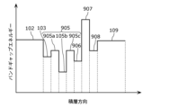
- FIG. 5 is a graph showing the distribution of the bandgap energy in the stacking direction of the semiconductor stack according to the present embodiment.
- the nitride semiconductor light emitting device includes a substrate 101, a semiconductor laminate, a current blocking layer 111, and a P-side electrode 112. and an N-side electrode 113 .
- the semiconductor laminate according to this embodiment includes an N-type cladding layer 102, a first N-side guide layer 203, a second N-side guide layer 104, an active layer 105, and a second It has one P-side guide layer 106, an electron barrier layer 107, a second P-side guide layer 108, a P-type cladding layer 109, and a contact layer 110 (see FIG. 2A).
- the first N-side guide layer 203 is an example of a first guide layer, which is an optical guide layer arranged between the N-type cladding layer 102 and the active layer 105, and is made of AlGaInN. That is, the first N-side guide layer 203 is an example of the first semiconductor layer and an example of the N-side semiconductor layer. The first N-side guide layer 203 has a higher refractive index and a lower bandgap energy than the N-type clad layer 102 . Also, the first N-side guide layer 203 is an N-type nitride semiconductor layer. The average bandgap energy of the first N-side guide layer 203 is greater than the average bandgap energy of the second P-side guide layer 108 .
- the first N-side guide layer 203 is arranged between the N-type cladding layer 102 and the second N-side guide layer 104, and is a film doped with Si at a concentration of 5 ⁇ 10 17 cm ⁇ 3 . It is an N-type Al 0.06 Ga 0.93 In 0.01 N layer with a thickness of 70 nm.
- the first N-side guide layer 203 is made of AlGaInN, so that the tensile strain of the semiconductor laminate with respect to the substrate 101 can be further reduced.
- the semiconductor laminate according to the present embodiment is laminated on the substrate 101 using epitaxial growth technology by the MOCVD method in the same manner as the semiconductor laminate 100S according to the first embodiment.
- each layer made of AlGaN (the N-type cladding layer 102, the electron barrier layer 107, the second P-side guide layer 108, the P-type cladding layer 109, and the contact layer 110) is For example, the crystal is grown at 1150°C.
- each layer containing In (the first N-side guide layer 203, the second N-side guide layer 104, the active layer 105, and the first P-side guide layer 106) has a temperature lower than that of each layer made of AlGaN, for example, at 850°C.
- the crystal is grown at the growth rate.
- FIG. 6 is a graph showing the distribution of the bandgap energy in the stacking direction of the semiconductor stack according to the present embodiment.
- the nitride semiconductor light emitting device includes a substrate 101, a semiconductor laminate, a current blocking layer 111, and a P-side electrode 112. and an N-side electrode 113 .
- the semiconductor laminate according to the present embodiment includes a first N-type clad layer 302a, a second N-type clad layer 302b, a third N-type clad layer 302c, and a first N-side clad layer 302a.
- the active layer 305 has two barrier layers 105a and 105c and a well layer 305b.
- the first N-type clad layer 302a is arranged above the substrate 101 and is an example of the first clad layer made of AlGaN, and is also an example of the N-type clad layer.
- the conductivity type of the first N-type cladding layer 302a is N-type.
- the first N-type cladding layer 302a has a lower refractive index and a higher average bandgap energy than the active layer 305 .
- the first N-type cladding layer 302a is disposed between the substrate 101 and the second N-type cladding layer 302b, and is doped with Si at a concentration of 5 ⁇ 10 17 cm ⁇ 3 and has a thickness of 350 nm. It is an N-type Al 0.065 Ga 0.935 N layer.
- the second N-type cladding layer 302b is arranged between the first N-type cladding layer 302a and the active layer 305, and is an example of a first semiconductor layer made of AlGaInN and an example of an N-side semiconductor layer.
- the second N-type clad layer 302b is an N-type clad layer.
- the average bandgap energy of the second N-type cladding layer 302b is smaller than the average bandgap energy of the first N-type cladding layer 302a and the bandgap energy of the barrier layer 105a.
- the Al composition ratio of the second N-type clad layer 302b is higher than the Al composition ratio of the first N-type clad layer 302a.
- the second N-type cladding layer 302b is located between the first N-type cladding layer 302a and the third N-type cladding layer 302c and is doped with Si at a concentration of 5 ⁇ 10 17 cm ⁇ 3 . It is an N-type Al 0.17 Ga 0.78 In 0.05 N layer with a thickness of 100 nm.
- the third N-type clad layer 302c is arranged above the substrate 101 and is an example of a first clad layer made of AlGaN and an example of an N-type clad layer.
- the third N-type cladding layer 302c has a lower refractive index and a higher average bandgap energy than the active layer 305.
- FIG. In this embodiment, the third N-type cladding layer 302c is arranged between the second N-type cladding layer 302b and the first N-side guide layer 303, and is doped with Si at a concentration of 5 ⁇ 10 17 cm ⁇ 3 . It is an N-type Al 0.065 Ga 0.935 N layer with a thickness of 350 nm.
- the first N-side guide layer 303 is an example of a first guide layer, which is an optical guide layer arranged between the first N-type cladding layer 302a and the active layer 305, and is made of AlGaInN. That is, the first N-side guide layer 303 is an example of the first semiconductor layer as well as an example of the N-side semiconductor layer.
- the first N-side guide layer 303 has a higher refractive index and a lower bandgap energy than the first N-type cladding layer 302a. Also, the first N-side guide layer 303 is an N-type nitride semiconductor layer.
- the first N-side guide layer 303 is arranged between the third N-type cladding layer 302c and the second N-side guide layer 304, and is doped with Si at a concentration of 5 ⁇ 10 17 cm ⁇ 3 . It is an N-type Al 0.159 Ga 0.791 In 0.05 N layer with a thickness of 70 nm.
- the second N-side guide layer 304 is arranged above the first N-type cladding layer 302a and is an example of an N-side semiconductor layer made of a nitride-based semiconductor.
- the second N-side guide layer 304 is arranged between the first N-type cladding layer 302a and the active layer 305, and is also an example of the first semiconductor layer made of AlGaInN.
- the second N-side guide layer 304 is an optical guide layer.
- the average bandgap energy of the second N-side guide layer 304 is smaller than the average bandgap energy of the first N-type cladding layer 302a.
- the second N-side guide layer 304 is an undoped AlGaInN layer.
- the average bandgap energy, Al composition ratio, and In composition ratio of the first N-side guide layer 303 are equal to the average bandgap energy, Al composition ratio, and In composition ratio of the second N-side guide layer 304, respectively.
- the second N-side guide layer 304 is composed of undoped Al 0.159 Ga 0.791 In 0.05 with a thickness of 70 nm, which is arranged between the first N-side guide layer 303 and the active layer 305 . N layer.
- the well layer 305b is a nitride-based semiconductor layer arranged above the barrier layer 105a and functioning as a well of a quantum well structure.
- the well layer 305b is an undoped Al 0.02 Ga 0.96 In 0.02 N layer with a thickness of 17.5 nm.
- the first P-side guide layer 306 is arranged above the active layer 305 and is an example of a P-side semiconductor layer made of a nitride-based semiconductor.
- the first P-side guide layer 306 is arranged between the P-type cladding layer 109 and the active layer 305, and is also an example of the first semiconductor layer made of AlGaInN.
- the first P-side guide layer 306 is a light guide layer.
- the average bandgap energy of the first P-side guide layer 306 is smaller than the average bandgap energy of the P-type cladding layer 109 .
- the first P-side guide layer 306 is an undoped AlGaInN layer.
- the first P-side guide layer 306 is an undoped Al 0.159 Ga 0.791 In 0.05 N layer with a thickness of 72 nm disposed between the active layer 305 and the electron barrier layer 107. be.
- the average bandgap energy, Al composition ratio, and In composition ratio of the second N-side guide layer 304 are equal to the average bandgap energy, Al composition ratio, and In composition ratio of the first P-side guide layer 306, respectively.
- the average bandgap energy of the first P-side guide layer 306 is equal to the average bandgap energy of the second P-side guide layer 108 .
- the first N-side guide layer 303 is made of AlGaInN, so that the tensile strain of the semiconductor laminate with respect to the substrate 101 can be further reduced.
- the N-type cladding layer is made of AlGaInN, the tensile strain of the semiconductor laminate with respect to the substrate 101 can be further reduced.
- the second N-type cladding layer 302b made of AlGaInN is crystal-grown at 850.degree. Therefore, for example, the crystal growth takes longer than in the semiconductor stacked body 100S according to the first embodiment.
- only the second N-type cladding layer 302b, which is a part of the cladding layer is made of AlGaInN instead of the entire cladding layer.
- the Al composition ratio of the first semiconductor layer is higher than the Al composition ratio of the first N-type clad layer 302a and the P-type clad layer 109, so the In composition ratio of the first semiconductor layer can be increased. Therefore, the tensile strain of the semiconductor laminate with respect to the substrate 101 can be reduced.
- the second N-type cladding layer 302b, the first N-side guide layer 303, the second N-side guide layer 304, and the first P-side guide layer 306, which are each an example of the first semiconductor layer, are provided. has a compressive strain with respect to the substrate 101 .
- the second N-type cladding layer 302b, the first N-side guide layer 303, and the second N-side guide layer 304, which are examples of the N-side semiconductor layers, and the first N-type cladding layer 302b, which are examples of the P-side semiconductor layers, are examples of the P-side semiconductor layers.
- the lattice constant of AlGaInN included in the P-side guide layer 306 is larger than the lattice constant of GaN included in the substrate 101 .
- the bandgap energy of the first semiconductor layer is greater than the bandgap energy of GaN forming the substrate 101 .
- other layers of the semiconductor laminate have tensile strain with respect to the substrate 101 . Therefore, since each layer has a compressive strain, the tensile strain of the semiconductor laminate with respect to the substrate 101 can be further reduced, and the absorption of light generated in the active layer 305 can be suppressed.
- the Al composition ratio of the first semiconductor layer is higher than the Al composition ratio of the barrier layers 105a and 105c, the In composition ratio of the first semiconductor layer can be increased. Therefore, the tensile strain of the semiconductor laminate with respect to the substrate 101 can be reduced.
- the first P-side guide layer 306 arranged between the electron barrier layer 107 and the active layer 305 has compressive strain, a piezoelectric field can be formed from the electron barrier layer 107 to the active layer 305 . Thereby, the efficiency of injecting holes into the active layer 305 can be improved.
- the second N-type cladding layer 302b, the first N-side guide layer 303, the second N-side guide layer 304, and the first P-side guide layer 306, which are each an example of the first semiconductor layer, are provided. are higher than those of the barrier layers 105a and 105c.
- the Al composition ratios of the second N-type cladding layer 302b, the first N-side guide layer 303, the second N-side guide layer 304, and the first P-side guide layer 306, each of which is an example of the first semiconductor layer are , the Al composition ratio of the barrier layers 105a and 105c or less. Thereby, the tensile strain of the semiconductor laminate with respect to the substrate 101 can be reduced.
- the well layer 305b is made of AlGaInN, fluctuations in the In composition ratio in the well layer 305b cause localization of carriers and improve luminous efficiency.
- the piezoelectric field can be reduced by reducing the compressive strain, so it is possible to increase the internal quantum efficiency and reduce the long wavelength shift of the oscillation wavelength.
- FIG. 7 is a graph showing the distribution of the bandgap energy in the stacking direction of the semiconductor stack according to the present embodiment.
- the nitride-based semiconductor light-emitting device includes a substrate 101, a semiconductor laminate, a current blocking layer 111, and a P-side electrode 112, similarly to the nitride-based semiconductor light-emitting device according to the third embodiment. , and an N-side electrode 113 .
- the semiconductor laminate according to this embodiment includes a first N-type clad layer 302a, a second N-type clad layer 302b, a third N-type clad layer 302c, and a first N-side clad layer 302a.
- a guide layer 303 a guide layer 303, a second N-side guide layer 304, an active layer 305, a first P-side guide layer 406, an electron barrier layer 107, a second P-side guide layer 108, a P-type cladding layer 109, and a contact layer 110 (see FIG. 2A).
- the first P-side guide layer 406 is arranged above the active layer 305 and is an example of a P-side semiconductor layer made of a nitride-based semiconductor.
- the first P-side guide layer 406 is arranged between the P-type cladding layer 109 and the active layer 305, and is also an example of a first semiconductor layer made of AlGaInN.
- the first P-side guide layer 406 is an undoped Al 0.18 Ga 0.76 In 0.06 N layer with a thickness of 72 nm disposed between the active layer 305 and the electron barrier layer 107. be.
- the bandgap energy of the first P-side guide layer 406 is smaller than the bandgap energies of the first N-side guide layer 303 and the second N-side guide layer 304 . Also, the In composition ratio of the first P-side guide layer 406 is higher than the In composition ratios of the first N-side guide layer 303 and the second N-side guide layer 304 .
- the compressive strain of the first P-side guide layer 406 becomes larger than the compressive strain of the first N-side guide layer 303 and the second N-side guide layer 304 . Accordingly, the piezoelectric field from the electron barrier layer 107 to the active layer 305 becomes larger than the piezoelectric field from the active layer 305 to the N-type clad layers such as the first N-type clad layer 302a. Therefore, the efficiency of injecting holes into the active layer 305 can be improved. Since holes have a larger effective mass than electrons, holes generally tend to have lower injection efficiency than electrons.
- the piezoelectric field from the electron barrier layer 107 to the active layer 305 is applied to the active layer
- the piezoelectric field from 305 to the N-type cladding layers, such as the first N-type cladding layer 302a, can be greater than the piezoelectric field. Therefore, the injection efficiency of holes, which tends to be lower than that of electrons, can be increased.
- FIG. 8 is a graph showing the distribution of the bandgap energy in the stacking direction of the semiconductor stack according to the present embodiment.
- the nitride-based semiconductor light-emitting device includes a substrate 101, a semiconductor laminate, a current blocking layer 111, and a P-side electrode 112, similarly to the nitride-based semiconductor light-emitting device according to the first embodiment. , and an N-side electrode 113 . As shown in FIG.
- the semiconductor laminate according to this embodiment includes an N-type cladding layer 102, a first N-side guide layer 103, a second N-side guide layer 104, an active layer 105, and a second It has one P-side guide layer 106, a third P-side guide layer 506, an electron barrier layer 107, a second P-side guide layer 108, a P-type cladding layer 109, and a contact layer 110 (see FIG. 2A). .
- the semiconductor laminated body according to the present embodiment differs from the semiconductor laminated body 100S according to the first embodiment in that the third P-side guide layer 506 is provided.
- the third P-side guide layer 506 is an example of a first guide layer, which is an optical guide layer arranged between the P-type cladding layer 109 and the active layer 105, and is made of a nitride-based semiconductor.
- the third P-side guide layer 506 has a higher refractive index and a lower bandgap energy than the P-type cladding layer 109 .
- the average bandgap energy of the third P-side guide layer 506 is greater than or equal to the average bandgap energy of the first P-side guide layer 106 .
- the third P-side guide layer 506 contains Al.
- the third P-side guide layer 506 is a P-type nitride semiconductor layer.
- the third P-side guide layer 506 is disposed between the first P-side guide layer 106 and the electron barrier layer 107, and is doped with Mg at a concentration of 1 ⁇ 10 18 cm ⁇ 3 to a thickness of It is a 70 nm P-type Al 0.03 Ga 0.97 N layer.
- the refractive index and average bandgap energy of the third P-side guide layer 506 are equal to the refractive index and average bandgap energy of the second P-side guide layer 108, respectively.
- the nitride-based semiconductor light-emitting device having such a configuration also has the same effect as the nitride-based semiconductor light-emitting device 100 according to the first embodiment.
- FIG. 9 is a graph showing the distribution of the bandgap energy in the stacking direction of the semiconductor stack according to the present embodiment.
- the nitride-based semiconductor light-emitting device includes a substrate 101, a semiconductor laminate, a current blocking layer 111, and a P-side electrode 112, similarly to the nitride-based semiconductor light-emitting device according to the first embodiment. , and an N-side electrode 113 .
- the semiconductor laminate according to this embodiment includes an N-type cladding layer 102, a first N-side guide layer 103, a second N-side guide layer 104, an active layer 105, and a second It has one P-side guide layer 606, an electron barrier layer 107, a second P-side guide layer 108, a P-type cladding layer 109, and a contact layer 110 (see FIG. 2A).
- the semiconductor laminate according to the present embodiment is similar to that of Embodiment 1 in that the Al composition ratio of the first P-side guide layer 606 includes an Al composition gradient region in which the Al composition ratio increases monotonously as the distance from the active layer 105 increases. It is different from the semiconductor laminate 100S.
- the first P-side guide layer 606 is arranged above the active layer 105 and is an example of a P-side semiconductor layer made of a nitride-based semiconductor.
- the first P-side guide layer 606 is arranged between the P-type cladding layer 109 and the active layer 105, and is also an example of a first semiconductor layer made of AlGaInN.
- the average bandgap energy of the first P-side guide layer 606 is smaller than the average bandgap energy of the P-type cladding layer 109 .
- the first P-side guide layer 606 is an undoped AlGaInN layer with a thickness of 72 nm.
- the Al composition ratio of the first P-side guide layer 606 is represented by Xpg1.
- the Al composition ratios Xpg1 near and far from the active layer 105 of the first P-side guide layer 606 are 5.0% and 5.6%, respectively.
- the In composition ratio in the first P-side guide layer 606 is 1.0% and is uniform within the layer. That is, the composition of the first P-side guide layer 606 is Al 0.05 Ga 0.94 In 0.01 N at the interface closer to the active layer 105 and Al 0.056Ga0.934In0.01N .
- the first P-side guide layer 606 has the same bandgap energy as the second N-side guide layer 104 at the interface closer to the active layer 105, and the second P-side guide layer 606 at the interface farther from the active layer 105. It has the same bandgap energy as layer 108 .
- the nitride-based semiconductor light-emitting device having such a configuration also has the same effect as the nitride-based semiconductor light-emitting device 100 according to the first embodiment.
- the refractive index can be increased with distance from the active layer 105 . Therefore, since the refractive index of the region near the active layer 105 in the first P-side guide layer 606 can be increased, the peak position of the light intensity distribution in the stacking direction can be brought closer to the center of the active layer 105 in the stacking direction. This can increase the optical confinement factor.
- the entire first P-side guide layer 606 is the Al composition gradient region. It can be a region.
- FIG. 10 is a graph showing the distribution of the bandgap energy in the stacking direction of the semiconductor stack according to the present embodiment.
- the nitride-based semiconductor light-emitting device includes a substrate 101, a semiconductor laminate, a current blocking layer 111, and a P-side electrode 112, similarly to the nitride-based semiconductor light-emitting device according to the first embodiment. , and an N-side electrode 113 .
- the semiconductor laminate according to this embodiment includes an N-type cladding layer 102, a first N-side guide layer 703, a second N-side guide layer 104, an active layer 305, and a It has one P-side guide layer 706, an electron barrier layer 107, a second P-side guide layer 108, a P-type cladding layer 109, and a contact layer 110 (see FIG. 2A).
- the configuration of the active layer 305 according to this embodiment is the same as the configuration of the active layer 305 according to the third embodiment.
- the first N-side guide layer 703 is an example of a first guide layer, which is an optical guide layer arranged between the N-type cladding layer 102 and the active layer 305, and is made of AlGaInN. That is, the first N-side guide layer 703 is an example of the first semiconductor layer as well as an example of the N-side semiconductor layer. The first N-side guide layer 703 has a higher refractive index and a lower bandgap energy than the N-type clad layer 102 . Also, the first N-side guide layer 703 is an N-type nitride semiconductor layer.
- the first N-side guide layer 703 is arranged between the N-type cladding layer 102 and the second N-side guide layer 104, and is a film doped with Si at a concentration of 5 ⁇ 10 17 cm ⁇ 3 . It is an N-type Al 0.05 Ga 0.94 In 0.01 N layer with a thickness of 70 nm.
- the average bandgap energy, Al composition ratio, and In composition ratio of the first N-side guide layer 703 are equal to the average bandgap energy, Al composition ratio, and In composition ratio of the second N-side guide layer 104, respectively.
- the first P - side guide layer 706 is undoped Al0.154Ga0.796In0.05N .
- the average bandgap energy of each of the first N-side guide layer 703 and the second N-side guide layer 104 is equal to the average bandgap energy of the first P-side guide layer 706 .
- the average bandgap energy of each of the first N-side guide layer 703 , the second N-side guide layer 104 , and the first P-side guide layer 706 is smaller than the average bandgap energy of the second P-side guide layer 108 .
- the nitride-based semiconductor light-emitting device has the above configuration, so that the barrier layer 105a to the first P-side guide layer 706 have compressive strain with respect to the substrate 101.
- layer has a tensile strain.
- the first P-side guide layer 706 has compressive strain with respect to the substrate 101, whereby a piezoelectric field can be formed from the electron barrier layer 107 toward the active layer 305, thereby increasing hole injection efficiency.
- FIG. 11 is a graph showing the distribution of the bandgap energy in the stacking direction of the semiconductor stack according to the present embodiment.
- the nitride-based semiconductor light-emitting device includes a substrate 101, a semiconductor laminate, a current blocking layer 111, and a P-side electrode 112, similarly to the nitride-based semiconductor light-emitting device according to the sixth embodiment. , and an N-side electrode 113 .
- the semiconductor laminate according to this embodiment includes an N-type cladding layer 102, a first N-side guide layer 103, a second N-side guide layer 104, an active layer 305, and a It has one P-side guide layer 806, an electron barrier layer 107, a second P-side guide layer 108, a P-type cladding layer 109, and a contact layer 110 (see FIG. 2A).
- the configuration of the active layer 305 according to this embodiment is the same as the configuration of the active layer 305 according to the third embodiment.
- the first P-side guide layer 806 is arranged above the active layer 305 and is an example of a P-side semiconductor layer made of a nitride-based semiconductor.
- the first P-side guide layer 806 is arranged between the P-type cladding layer 109 and the active layer 305 and is also an example of the first semiconductor layer made of AlGaInN.
- the average bandgap energy of the first P-side guide layer 806 is smaller than the average bandgap energy of the P-type cladding layer 109 .
- the first P-side guide layer 806 is an undoped AlGaInN layer with a thickness of 72 nm.
- the first P-side guide layer 806 includes a compositionally graded region whose composition changes with increasing distance from the active layer 305 .
- the Al composition ratio and In composition ratio of the first P-side guide layer 806 are represented by Xpg1 and Ypg1, respectively.
- the Al composition ratios Xpg1 near and far from the active layer 305 of the first P-side guide layer 806 are 15.4% and 5.6%, respectively.
- the In composition ratios Ypg1 near and far from the active layer 305 of the first P-side guide layer 806 are 5.0% and 1.0%, respectively. That is, the composition of the first P-side guide layer 806 is Al 0.154 Ga 0.796 In 0.05 N at the interface closer to the active layer 305 and Al 0.056Ga0.934In0.01N . _
- Such a first P-side guide layer 806 has compressive strain near the interface with the active layer 305 and tensile strain near the interface with the electron barrier layer 107 .
- the entire first P-side guide layer 806 is the compositionally graded region. There may be.
- FIG. 12 is a graph showing the distribution of the bandgap energy in the stacking direction of the semiconductor stack according to the present embodiment.
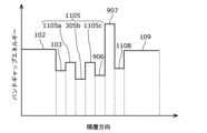
- the nitride-based semiconductor light-emitting device includes a substrate 101, a semiconductor laminate, a current blocking layer 111, and a P-side electrode 112, similarly to the nitride-based semiconductor light-emitting device according to the first embodiment. , and an N-side electrode 113 .
- the semiconductor laminate according to this embodiment includes an N-type cladding layer 102, a first N-side guide layer 103, an active layer 905, a first P-side guide layer 906, an electron It has a barrier layer 907, a second P-side guide layer 908, a P-type cladding layer 109, and a contact layer 110 (see FIG. 2A).
- the first N-side guide layer 103 according to the present embodiment is an Al 0.03 GaN 0.97 layer like the first N-side guide layer 103 according to the first embodiment, but the film thickness and the impurity concentration is different.
- the first N-side guide layer 103 according to this embodiment is an undoped Al 0.03 GaN 0.97 layer with a thickness of 140 nm.
- the active layer 905 is arranged above the first N-side guide layer 103 and contacts the first N-side guide layer 103 .
- the active layer 905 has two barrier layers 905a and 905c and a well layer 105b.
- the well layer 105b is an undoped Ga 0.99 In 0.01 N layer with a thickness of 17.5 nm.
- Each of the barrier layers 905a and 905c is a nitride-based semiconductor layer arranged above the first N-side guide layer 103 and functioning as a barrier for the quantum well structure.
- Barrier layer 905c is disposed above barrier layer 905a.
- the bandgap energy of each of the barrier layers 905a and 905c is equal to the bandgap energy of the well layer 105b, the average bandgap energy of the first P-side guide layer 906, and the average bandgap energy of the first N-side guide layer 103. It is greater than the average bandgap energy and less than the average bandgap energy of electron barrier layer 907 .
- Each of the barrier layers 905a and 905c is an undoped Al 0.04 Ga 0.96 N layer with a thickness of 10 nm.
- the first P-side guide layer 906 is arranged above the active layer 905 and is an example of a P-side semiconductor layer made of a nitride-based semiconductor.
- the first P-side guide layer 906 is arranged between the P-type cladding layer 109 and the active layer 905, and is also an example of the first semiconductor layer made of AlGaInN. That is, in the nitride-based semiconductor light emitting device 100, the first P-side guide layer 103 (that is, N-side semiconductor layer) and the first P-side guide layer 906 (that is, P-side semiconductor layer) Only the guide layer 906 consists of AlGaInN.
- the first P-side guide layer 906 is a light guide layer.
- the average bandgap energy of the first P-side guide layer 906 is smaller than the average bandgap energy of the P-type cladding layer 109 .
- the first P-side guide layer 906 is an undoped AlGaInN layer.
- the first P-side guide layer 906 is an undoped Al 0.04 Ga 0.9516 In 0.0084 N layer with a thickness of 72 nm.
- the electron barrier layer 907 is a nitride semiconductor layer arranged between the first P-side guide layer 906 and the P-type cladding layer 109 .
- the bandgap energy of electron barrier layer 907 is greater than the bandgap energy of barrier layer 905c. This can suppress leakage of electrons from the active layer 905 to the P-type cladding layer 109 .
- the bandgap energy of electron barrier layer 907 is greater than the bandgap energy of P-type cladding layer 109 .
- the electron barrier layer 907 is a 5 nm thick P-type Al 0.36 Ga 0.64 N layer doped with Mg at a concentration of 1 ⁇ 10 19 cm ⁇ 3 .
- the second P-side guide layer 908 is an example of a first guide layer, which is an optical guide layer arranged between the P-type cladding layer 109 and the active layer 905, and is made of a nitride-based semiconductor.
- the second P-side guide layer 908 is also an example of a second guide layer arranged between the electron barrier layer 907 and the P-type cladding layer 109 .
- the second P-side guide layer 908 has a higher refractive index and a lower bandgap energy than the P-type cladding layer 109 .
- the average bandgap energy of the second P-side guide layer 908 is greater than or equal to the average bandgap energy of the first P-side guide layer 906 .
- the second P-side guide layer 908 contains Al.
- the second P-side guide layer 908 is a P-type nitride semiconductor layer.
- the second P-side guide layer 908 is disposed between the electron barrier layer 907 and the P-type cladding layer 109, and is doped with Mg at a concentration of 1 ⁇ 10 18 cm ⁇ 3 and has a thickness of 148 nm. It is a P-type Al 0.04 Ga 0.96 N layer.
- the average bandgap energy of the second P-side guide layer 908 is equal to the average bandgap energy of each of the barrier layers 905a and 905c.
- the first P-side guide layer 906 of the first N-side guide layer 103 and the first P-side guide layer 906 is made of AlGaInN
- Tensile strain of the semiconductor laminate can be reduced.
- the first N-side guide layer 103 and the first P-side guide layer 906 only the first N-side guide layer 103 may be made of AlGaInN.
- the first P-side guide layer 906 is also made of AlGaInN, so the tensile strain of the semiconductor laminate with respect to the substrate 101 can be reduced.
- the barrier layers 905a and 905c may be made of AlGaN.
- the first P-side guide layer 906 is also made of AlGaInN, so the tensile strain of the semiconductor laminate with respect to the substrate 101 can be reduced.
- the first P-side guide layer 906 is made of AlGaInN
- the first N-side guide layer 103 is made of AlGaN.
- the In composition ratio of the first P-side guide layer 906 is higher than the In composition ratio of the first N-side guide layer 103 .
- the tensile strain of the first P-side guide layer 906 with respect to the substrate 101 is smaller than the tensile strain of the first N-side guide layer 103 .
- the piezoelectric field from active layer 905 to electron barrier layer 907 is smaller than the piezoelectric field from N-type cladding layer 102 to active layer 905 . Therefore, as in the fourth embodiment, the injection efficiency of holes, which tends to be lower than that of electrons, can be increased.
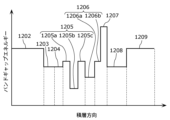
- FIG. 13 is a graph showing the distribution of the bandgap energy in the stacking direction of the semiconductor stack according to the present embodiment.
- the nitride-based semiconductor light-emitting device includes a substrate 101, a semiconductor laminate, a current blocking layer 111, and a P-side electrode 112, similarly to the nitride-based semiconductor light-emitting device according to the ninth embodiment. , and an N-side electrode 113 .
- the semiconductor laminate according to this embodiment includes an N-type cladding layer 1002, a first N-side guide layer 1003, an active layer 1005, a first P-side guide layer 1006, an electron It has a barrier layer 907, a second P-side guide layer 1008, a P-type cladding layer 1009, and a contact layer 110 (see FIG. 2A).
- the N-type clad layer 1002 is an example of a first clad layer arranged above the substrate 101 and made of AlGaN.
- the conductivity type of the N-type cladding layer 1002 is N-type.
- the N-type cladding layer 1002 has a lower refractive index and a higher average bandgap energy than the active layer 1005 .
- the N-type cladding layer 1002 is an N-type Al 0.10 Ga 0.90 N layer with a thickness of 800 nm doped with Si at a concentration of 5 ⁇ 10 17 cm ⁇ 3 .
- the first N-side guide layer 1003 is an example of a first guide layer, which is an optical guide layer arranged between the N-type cladding layer 1002 and the active layer 1005, and is made of a nitride semiconductor.
- the first N-side guide layer 1003 has a higher refractive index and a lower bandgap energy than the N-type cladding layer 1002 .
- the first N-side guide layer 1003 contains Al.
- the first N-side guide layer 1003 is an undoped nitride-based semiconductor layer.
- the first N-side guide layer 1003 is an undoped Al 0.05 Ga 0.95 N layer with a thickness of 70 nm arranged between the N-type cladding layer 1002 and the active layer 1005 .
- the active layer 1005 has a well layer 105b and two barrier layers 1005a and 1005c.
- Each of the barrier layers 1005a and 1005c is a nitride-based semiconductor layer arranged above the first N-side guide layer 1003 and functioning as a barrier for the quantum well structure.
- Barrier layer 1005c is disposed above barrier layer 1005a.
- the bandgap energy of each of the barrier layers 1005a and 1005c is equal to the bandgap energy of the well layer 105b, the average bandgap energy of the first P-side guide layer 1006, and the average bandgap energy of the first N-side guide layer 1003. It is greater than the average bandgap energy and less than the average bandgap energy of electron barrier layer 907 .
- Each of the barrier layers 1005a and 1005c is an undoped Al 0.07 Ga 0.93 N layer with a thickness of 10 nm.
- the first P-side guide layer 1006 is arranged above the active layer 1005 and is an example of a P-side semiconductor layer made of a nitride-based semiconductor. In this embodiment, the first P-side guide layer 1006 is arranged between the P-type cladding layer 1009 and the active layer 1005, and is also an example of the first semiconductor layer made of AlGaInN. In this embodiment, the first P-side guide layer 1006 is a light guide layer. The average bandgap energy of the first P-side guide layer 1006 is smaller than the average bandgap energy of the P-type cladding layer 1009 .
- the first P-side guide layer 1006 is an undoped AlGaInN layer. In this embodiment, the first P-side guide layer 1006 is an undoped Al 0.07 Ga 0.917 In 0.013 N layer with a thickness of 72 nm.
- the second P-side guide layer 1008 is an example of a first guide layer, which is an optical guide layer arranged between the P-type cladding layer 1009 and the active layer 1005, and is made of a nitride semiconductor.
- the second P-side guide layer 1008 is also an example of a second guide layer arranged between the electron barrier layer 907 and the P-type cladding layer 1009 .
- the second P-side guide layer 1008 has a higher refractive index and a lower bandgap energy than the P-type cladding layer 1009 .
- the average bandgap energy of the second P-side guide layer 1008 is greater than or equal to the average bandgap energy of the first P-side guide layer 1006 .
- the second P-side guide layer 1008 contains Al.
- the second P-side guide layer 1008 is a P-type nitride semiconductor layer.
- the second P-side guide layer 1008 is disposed between the electron barrier layer 907 and the P-type cladding layer 1009, and is doped with Mg at a concentration of 1 ⁇ 10 18 cm ⁇ 3 and has a thickness of 148 nm. It is a P-type Al 0.06 Ga 0.94 N layer.
- the P-type clad layer 1009 is an example of a first clad layer arranged above the substrate 101 and made of AlGaN.
- the conductivity type of the P-type cladding layer 1009 is P-type.
- the P-type cladding layer 1009 is arranged above the first P-side guide layer 1006 .
- the P-type cladding layer 1009 has a lower refractive index and a higher average bandgap energy than the active layer 1005 .
- the average bandgap energy of the P-type cladding layer 1009 is smaller than the average bandgap energy of the electron barrier layer 907 .
- the P-type clad layer 1009 is doped with Mg as an impurity.
- the impurity concentration at the end portion of the P-type cladding layer 1009 closer to the active layer 1005 is lower than the impurity concentration at the end portion farther from the active layer 1005 .
- the P-type cladding layer 1009 is an AlGaN layer with a thickness of 450 nm, and a P-type cladding layer with a thickness of 150 nm doped with Mg at a concentration of 2 ⁇ 10 18 cm ⁇ 3 located on the side closer to the active layer 1005 .
- the semiconductor laminate with respect to the substrate 101 is provided with the first P-side guide layer 1006 made of AlGaInN. Tensile strain of the laminate can be reduced.
- FIG. 14 is a graph showing the distribution of the bandgap energy in the stacking direction of the semiconductor stack according to the present embodiment.
- the nitride-based semiconductor light-emitting device includes a substrate 101, a semiconductor laminate, a current blocking layer 111, and a P-side electrode 112, similarly to the nitride-based semiconductor light-emitting device according to the ninth embodiment. , and an N-side electrode 113 .
- the semiconductor laminate according to this embodiment includes an N-type cladding layer 102, a first N-side guide layer 103, an active layer 1105, a first P-side guide layer 906, an electron It has a barrier layer 907, a second P-side guide layer 908, a P-type cladding layer 109, and a contact layer 110 (see FIG. 2A).
- the active layer 1105 has a well layer 305b and two barrier layers 1105a and 1105c.
- the well layer 305b is an undoped Al 0.02 Ga 0.96 In 0.02 N layer with a thickness of 17.5 nm.
- Each of the barrier layers 1105a and 1105c is a nitride-based semiconductor layer arranged above the first N-side guide layer 103 and functioning as a barrier for the quantum well structure.
- Barrier layer 1105c is disposed above barrier layer 1105a.
- the bandgap energy of each of the barrier layers 1105a and 1105c is equal to the bandgap energy of the well layer 305b, the average bandgap energy of the first P-side guide layer 906, and the average bandgap energy of the first N-side guide layer 103. It is greater than the average bandgap energy and less than the average bandgap energy of electron barrier layer 907 .
- Each of the barrier layers 1105a and 1105c is an undoped Al 0.07 Ga 0.92 In 0.02 N layer with a thickness of 10 nm.
- the nitride-based semiconductor light-emitting device according to the present embodiment also has the same effect as the nitride-based semiconductor light-emitting device according to the ninth embodiment.
- each layer of the active layer 1105 is made of AlGaInN, so that the Al composition ratio of the first P-side guide layer 906, which is an example of the first semiconductor layer, is the same as that of the barrier layer. It can be made lower than the Al composition ratio of 1105a and 1105c. Thereby, the tensile strain of the semiconductor laminate with respect to the substrate 101 can be further reduced.
- FIG. 15 is a graph showing the distribution of the bandgap energy in the stacking direction of the semiconductor stack according to the present embodiment.
- the nitride-based semiconductor light-emitting device includes a substrate 101, a semiconductor laminate, a current blocking layer 111, and a P-side electrode 112, similarly to the nitride-based semiconductor light-emitting device according to the first embodiment. , and an N-side electrode 113 .
- the semiconductor laminate according to this embodiment includes an N-type cladding layer 1202, a first N-side guide layer 1203, a second N-side guide layer 1204, an active layer 1205, and a It has one P-side guide layer 1206, an electron barrier layer 1207, a second P-side guide layer 1208, a P-type cladding layer 1209, and a contact layer 110 (see FIG. 2A).
- the N-type clad layer 1202 is an example of a first clad layer arranged above the substrate 101 and made of AlGaN.
- the conductivity type of the N-type cladding layer 1202 is N-type.
- the N-type cladding layer 1202 has a lower refractive index and a higher average bandgap energy than the active layer 1205 .
- the N-type cladding layer 1202 is an N-type Al 0.065 Ga 0.935 N layer with a thickness of 900 nm doped with Si at a concentration of 1 ⁇ 10 18 cm ⁇ 3 .
- the first N-side guide layer 1203 is an example of a first guide layer, which is an optical guide layer arranged between the N-type cladding layer 1202 and the active layer 1205, and is made of a nitride semiconductor.
- the first N-side guide layer 1203 has a higher refractive index and a lower bandgap energy than the N-type cladding layer 1202 .
- the first N-side guide layer 1203 contains Al.
- the first N-side guide layer 1203 is arranged between the N-type cladding layer 1202 and the second N-side guide layer 1204, and is a film doped with Si at a concentration of 1 ⁇ 10 18 cm ⁇ 3 . It is an N-type Al 0.03 Ga 0.97 N layer with a thickness of 127 nm.
- the second N-side guide layer 1204 is arranged above the N-type cladding layer 1202 and is an example of an N-side semiconductor layer made of a nitride-based semiconductor.
- the second N-side guide layer 1204 is a semiconductor layer made of AlGaN, arranged between the N-type cladding layer 1202 and the active layer 1205 .
- the second N-side guide layer 1204 is an optical guide layer.
- the average bandgap energy of the second N-side guide layer 1204 is smaller than the average bandgap energy of the N-type cladding layer 1202 .
- the second N-side guide layer 1204 is an undoped AlGaN layer.
- the average bandgap energy and Al composition ratio of the first N-side guide layer 1203 are equal to the average bandgap energy and Al composition ratio of the second N-side guide layer 1204, respectively.
- the second N-side guide layer 1204 is an undoped Al 0.03 Ga 0.97 N layer with a thickness of 80 nm arranged between the first N-side guide layer 1203 and the active layer 1205. .
- the active layer 1205 has a well layer 1205b and two barrier layers 1205a and 1205c.
- the structure of the well layer 1205b is determined so that the peak wavelength of photoluminescence from the nitride-based semiconductor light emitting device is 366 nm.
- the well layer 1205b is an undoped Ga 0.99 In 0.01 N layer with a thickness of 17.5 nm.
- the barrier layer 1205a is a nitride-based semiconductor layer arranged between the first N-side guide layer 1203 and the well layer 1205b and functioning as a barrier for the quantum well structure.
- the barrier layer 1205c is a nitride-based semiconductor layer arranged between the well layer 1205b and the first P-side guide layer 1206 and functioning as a barrier for the quantum well structure.
- the bandgap energy of each of the barrier layers 1205a and 1205c is equal to the bandgap energy of the well layer 1205b, the average bandgap energy of the first P-side guide layer 1206, and the average bandgap energy of the first N-side guide layer 1203.
- the barrier layer 1205a is an undoped Al 0.04 Ga 0.96 N layer with a thickness of 14 nm
- the barrier layer 1205c is an undoped Al 0.04 Ga 0.96 N layer with a thickness of 12 nm.
- the first P-side guide layer 1206 is arranged above the active layer 1205 and is an example of a P-side semiconductor layer made of a nitride-based semiconductor.
- the first P-side guide layer 1206 includes a lower first P-side guide layer 1206a and an upper first P-side guide layer 1206b.
- the lower first P-side guide layer 1206a is a layer that is arranged between the P-type cladding layer 1209 and the active layer 1205 and made of AlGaInN.
- the upper first P-side guide layer 1206b is arranged between the lower first P-side guide layer 1206a and the P-type cladding layer 1209 and is a layer made of AlGaN.
- the lower first P-side guide layer 1206 a is an example of a first semiconductor layer arranged between the P-type cladding layer 1209 made of AlGaN and the active layer 1205 .
- the lower first P-side guide layer 1206a is arranged above the active layer 1205 and is also an example of a P-side semiconductor layer made of a nitride-based semiconductor.
- the first P-side guide layer 1206 is a light guide layer.
- the average bandgap energy of each of the lower first P-side guide layer 1206 a and the upper first P-side guide layer 1206 b is smaller than the average bandgap energy of the P-type cladding layer 1209 .
- the first P-side guide layer 1206 is an undoped Al 0.04 Ga 0.95 In 0.01 N layer with a thickness of 53 nm, which is arranged between the active layer 1205 and the electron barrier layer 1207. and an upper first P-side guide layer 1206b which is an undoped Al 0.04 Ga 0.96 N layer with a thickness of 7 nm.
- the lower first P-side guide layer 1206 a has compressive strain with respect to the substrate 101 .
- the Mg concentration of the upper first P-side guide layer 1206b may increase toward the interface.
- the impurity concentration of the upper first P-side guide layer 1206b may not be uniform.
- the upper first P-side guide layer 1206b has a lower refractive index and a higher bandgap energy than the lower first P-side guide layer 1206a.
- the electron barrier layer 1207 is a nitride semiconductor layer arranged between the first P-side guide layer 1206 and the P-type clad layer 1209 .
- the bandgap energy of electron barrier layer 1207 is greater than the bandgap energy of barrier layer 1205c. This can suppress leakage of electrons from the active layer 1205 to the P-type clad layer 1209 .
- the bandgap energy of electron barrier layer 1207 is greater than the bandgap energy of P-type cladding layer 1209 .
- the electron barrier layer 1207 is a 1.6 nm thick P-type Al 0.36 Ga 0.64 N layer doped with Mg at a concentration of 1.5 ⁇ 10 19 cm ⁇ 3 .
- the second P-side guide layer 1208 is an example of a first guide layer, which is an optical guide layer arranged between the P-type cladding layer 1209 and the active layer 1205, and is made of a nitride semiconductor.
- the second P-side guide layer 1208 is also an example of a second guide layer arranged between the electron barrier layer 1207 and the P-type clad layer 1209 .
- the second P-side guide layer 1208 has a higher refractive index and a lower bandgap energy than the P-type cladding layer 1209 .
- the second P-side guide layer 1208 has a smaller refractive index and a larger bandgap energy than the lower first P-side guide layer 1206a.
- the second P-side guide layer 1208 has the same refractive index and the same bandgap energy as the second N-side guide layer 1204 .
- the second P-side guide layer 1208 contains Al.
- the second P-side guide layer 1208 is a P-type nitride semiconductor layer.
- the second P-side guide layer 1208 is disposed between the electron barrier layer 1207 and the P-type cladding layer 1209, and is doped with Mg at a concentration of 2 ⁇ 10 18 cm ⁇ 3 and has a thickness of 110 nm. It is a P-type Al 0.03 Ga 0.97 N layer.
- the P-type clad layer 1209 is an example of a first clad layer arranged above the substrate 101 and made of AlGaN.
- the conductivity type of the P-type cladding layer 1209 is P-type.
- the P-type cladding layer 1209 is arranged above the first P-side guide layer 1206 .
- the P-type cladding layer 1209 has a lower refractive index and a higher average bandgap energy than the active layer 1205 .
- the average bandgap energy of the P-type cladding layer 1209 is smaller than the average bandgap energy of the electron blocking layer 1207 .
- the P-type cladding layer 1209 is doped with Mg as an impurity.
- the impurity concentration at the end portion of the P-type cladding layer 1209 closer to the active layer 1205 is lower than the impurity concentration at the end portion farther from the active layer 1205 .
- the P-type cladding layer 1209 is an AlGaN layer with a thickness of 450 nm, and is placed on the side closer to the active layer 1205 and is doped with Mg at a concentration of 2 ⁇ 10 18 cm ⁇ 3 with a thickness of 150 nm.
- the tensile strain of the semiconductor laminate with respect to the substrate 101 can be reduced.
- the light confinement factor in the active layer 1205 is 5.2%
- the optical loss (that is, waveguide loss) is 3.8 cm ⁇ 1
- the effective refractive index is The index difference is 14.0 ⁇ 10 ⁇ 3 .
- the effective refractive index difference means the average refractive index of the region below the ridge (see ridge 109R in FIG. 2A) formed in the P-type cladding layer 1209, where light exists, and the average refractive index of the region below the ridge. It is the difference from the average refractive index of a region other than the region where light exists.
- the peak position of the light intensity distribution in the stacking direction should be positioned 11.3 nm above the interface between the second N-side guide layer 1204 and the barrier layer 1205a. can be done. As described above, in this embodiment, the peak position of the light intensity distribution in the stacking direction can be located near the well layer 1205b of the active layer 1205. FIG.
- the divergence angle of emitted light in the stacking direction is 44.7 degrees.
- the divergence angle is a parameter indicating the divergence angle of emitted light, and is determined so that the light intensity at the divergence angle is 1/ e2 of the light intensity on the optical axis.
- the bandgap energy of the lower first P-side guide layer 1206a made of AlGaInN should be greater than the bandgap energy of GaN and equal to or less than the bandgap energy of the second P-side guide layer 1208 .
- the refractive index of the lower first P-side guide layer 1206a is reduced to the second P while reducing the waveguide loss due to light absorption with respect to the laser oscillation wavelength. It can be greater than or equal to the refractive index of the side guide layer 1208 .
- the controllability of the maximum position of the peak intensity of the light distribution in the vertical direction to the position near the well layer can be improved, and low waveguide loss can be obtained while increasing the light confinement factor.
- a nitride-based semiconductor light-emitting device having good characteristics can be realized.
- the configuration of the nitride-based semiconductor light-emitting device according to this embodiment is not limited to the configuration example described above.
- the composition of the lower first P-side guide layer 1206a of the first P-side guide layer 1206 may be different from the configuration example described above. Modification 1, which differs from the above configuration example in the lower first P-side guide layer 1206a, will be described below.
- the lower first P-side guide layer 1206a is an undoped Al 0.04 Ga 0.945 In 0.015 N layer with a thickness of 53 nm.
- the lower first P-side guide layer 1206 a has compressive strain with respect to the substrate 101 .
- the nitride-based semiconductor light-emitting device according to Modification 1 also exhibits the same effects as the nitride-based semiconductor light-emitting device according to the present embodiment described above.
- the light confinement factor in the active layer 1205 is 4.8%
- the light loss is 4.3 cm ⁇ 1
- the effective refractive index difference is 12.9 ⁇ 10 -3 .
- the peak position of the light intensity distribution in the stacking direction can be positioned 3.5 nm above the interface between the second N-side guide layer 1204 and the barrier layer 1205a. can.
- the peak position of the light intensity distribution in the stacking direction can be located near the well layer 1205b of the active layer 1205.
- the divergence angle of emitted light in the stacking direction is 42.5 degrees.
- the configuration of the lower first P-side guide layer 1206a is not limited to this.
- the lower first P-side guide layer 1206a according to Modification 2 may be an undoped Al 0.04 Ga 0.945 In 0.015 N layer with a thickness of 25 nm.
- the light confinement factor in the active layer 1205 is 4.8%
- the optical loss is 4.7 cm ⁇ 1
- the effective refractive index difference is 13.7 cm ⁇ 1 . 9 ⁇ 10 ⁇ 3 .
- the peak position of the light intensity distribution in the stacking direction can be positioned 2.3 nm above the interface between the second N-side guide layer 1204 and the barrier layer 1205a. can.
- the peak position of the light intensity distribution in the stacking direction can be positioned near the well layer 1205b of the active layer 1205.
- the divergence angle of emitted light in the stacking direction is 42.4 degrees.
- a nitride-based semiconductor light-emitting device having excellent characteristics can be realized.
- FIG. 16 is a graph showing the distribution of the bandgap energy in the stacking direction of the semiconductor stack according to the present embodiment.
- the nitride-based semiconductor light-emitting device includes a substrate 101, a semiconductor laminate, a current blocking layer 111, and a P-side electrode 112, similarly to the nitride-based semiconductor light-emitting device according to the first embodiment. , and an N-side electrode 113 .
- the semiconductor laminate according to this embodiment includes an N-type cladding layer 1202, a first N-side guide layer 1203, a second N-side guide layer 1204, an active layer 1205, and a It has one P-side guide layer 1306, an electron barrier layer 1207, a second P-side guide layer 1208, a P-type cladding layer 1209, and a contact layer 110 (see FIG. 2A).
- the first P-side guide layer 1306 is arranged above the active layer 1205 and is an example of a P-side semiconductor layer made of a nitride-based semiconductor.
- the first P-side guide layer 1306 includes a lower first P-side guide layer 1306a and an upper first P-side guide layer 1206b.
- the lower first P-side guide layer 1306a is arranged between the P-type cladding layer 1209 and the active layer 1205 and is a layer made of AlGaInN.
- the upper first P-side guide layer 1206b is a layer that is arranged between the lower first P-side guide layer 1306a and the P-type cladding layer 1209 and made of AlGaN.
- the lower first P-side guide layer 1306 a is an example of a first semiconductor layer arranged between the P-type cladding layer 1209 made of AlGaN and the active layer 1205 .
- the lower first P-side guide layer 1206a is arranged above the active layer 1205 and is also an example of a P-side semiconductor layer made of a nitride-based semiconductor.
- the first P-side guide layer 1306 according to this embodiment differs from the first P-side guide layer 1206 according to the twelfth embodiment in the In composition ratio of the lower first P-side guide layer 1306a.
- the first P-side guide layer 1306 is an undoped Al 0.04 Ga 0.955 In 0.005 N layer with a thickness of 53 nm, which is arranged between the active layer 1205 and the electron barrier layer 1207 . and an upper first P-side guide layer 1206b which is an undoped Al 0.04 Ga 0.96 N layer with a thickness of 7 nm.
- Lower first P-side guide layer 1306 a has tensile strain with respect to substrate 101 .
- the lower first P-side guide layer 1306a and the second P-side guide layer 1208 have substantially the same refractive index and the same bandgap energy.
- the nitride-based semiconductor light-emitting device according to the present embodiment having the configuration as described above also has excellent characteristics similar to the nitride-based semiconductor light-emitting device according to the twelfth embodiment. can be realized.
- the nitride-based semiconductor light-emitting device is a semiconductor laser device, but the nitride-based semiconductor light-emitting device is not limited to a semiconductor laser device.
- the nitride-based semiconductor light emitting device may be a superluminescent diode.
- the reflectance of the end surface of the semiconductor laminate included in the nitride-based semiconductor light-emitting device with respect to the emitted light from the semiconductor laminate may be 0.1% or less.
- Such a reflectance can be realized, for example, by forming an antireflection film made of a dielectric multilayer film or the like on the end face.
- the guided light reflected by the front end face is coupled again with the waveguide to form a guided light component.
- the P-type clad layer is a layer with a uniform Al composition ratio, but the configuration of the P-type clad layer is not limited to this.
- the P-type cladding layer may have a superlattice structure in which each of a plurality of AlGaN layers and each of a plurality of GaN layers are alternately laminated.
- each embodiment has the second P-side guide layer, it may not have the second P-side guide layer.
- the nitride-based semiconductor light emitting device has both the first N-side guide layer and the first P-side guide layer. It is not necessary to have one P-side guide layer. Alternatively, it may have the first P-side guide layer and not have the first N-side guide layer.
- the N-type clad layer is laminated on the substrate 101, but another layer may be inserted between the substrate 101 and the N-type clad layer.
- another layer may be inserted between the substrate 101 and the N-type clad layer.
- a buffer layer, an underlying layer, or the like may be inserted between the substrate 101 and the N-type clad layer.
- the nitride-based semiconductor light-emitting device of the present disclosure can be applied, for example, as a high-output and high-efficiency light source to light sources for exposure apparatuses and processing machines.
- REFERENCE SIGNS LIST 100 nitride-based semiconductor light-emitting device 100F, 100R end surface 100S semiconductor laminate 101 substrate 102, 1002, 1202 N-type clad layer 103, 203, 303, 703, 1003, 1203 first N-side guide layer 104, 304, 1204 second N-side guide layers 105, 305, 905, 1005, 1105, 1205 active layers 105a, 105c, 905a, 905c, 1005a, 1005c, 1105a, 1105c, 1205a, 1205c barrier layers 105b, 305b, 1205b well layers 106, 306, 406 , 606, 706, 806, 906, 1006, 1206, 1306 First P-side guide layer 107, 907, 1207 Electron barrier layer 108, 908, 1008, 1208 Second P-side guide layer 109, 1009, 1209 P-type clad layer 109R ridge 109T groove 110 contact layer 111 current blocking layer 112 P-side electrode 113 N-
Landscapes
- Engineering & Computer Science (AREA)
- Physics & Mathematics (AREA)
- Manufacturing & Machinery (AREA)
- Computer Hardware Design (AREA)
- Microelectronics & Electronic Packaging (AREA)
- Power Engineering (AREA)
- Condensed Matter Physics & Semiconductors (AREA)
- General Physics & Mathematics (AREA)
- Electromagnetism (AREA)
- Optics & Photonics (AREA)
- Semiconductor Lasers (AREA)
Abstract
La présente invention concerne un élément électroluminescent à semi-conducteur au nitrure (100) qui comprend : un substrat (1010) comprenant du GaN ; une première couche de gaine comprenant de l'AlGaN disposée au-dessus du substrat (101) ; une couche active (105) disposée au-dessus du substrat (101) ; et une première couche semi-conductrice disposée entre la première couche de gaine et la couche active (105). La couche active (105) présente une couche de puits (105b) comprenant un semi-conducteur au nitrure et des couches barrières (105a) et (105c) comprenant un semi-conducteur au nitrure contenant de l'Al. L'énergie de bande interdite moyenne de la première couche semi-conductrice est inférieure à l'énergie de bande interdite moyenne de la première couche de gaine et la première couche semi-conductrice comprend de l'AlGaInN.
Applications Claiming Priority (2)
| Application Number | Priority Date | Filing Date | Title |
|---|---|---|---|
| JP2022020111 | 2022-02-14 | ||
| JP2022-020111 | 2022-02-14 |
Publications (1)
| Publication Number | Publication Date |
|---|---|
| WO2023153035A1 true WO2023153035A1 (fr) | 2023-08-17 |
Family
ID=87564058
Family Applications (1)
| Application Number | Title | Priority Date | Filing Date |
|---|---|---|---|
| PCT/JP2022/041910 WO2023153035A1 (fr) | 2022-02-14 | 2022-11-10 | Élément électroluminescent à semi-conducteur au nitrure |
Country Status (1)
| Country | Link |
|---|---|
| WO (1) | WO2023153035A1 (fr) |
Citations (4)
| Publication number | Priority date | Publication date | Assignee | Title |
|---|---|---|---|---|
| US20080259982A1 (en) * | 2007-04-20 | 2008-10-23 | Kim Chi Sun | Semiconductor laser diode formed with window at cleavage facet and fabricating method thereof |
| JP2010263163A (ja) * | 2009-05-11 | 2010-11-18 | Sumitomo Electric Ind Ltd | 窒化物半導体発光素子 |
| JP2011044596A (ja) * | 2009-08-21 | 2011-03-03 | Sharp Corp | 窒化物半導体素子及びその製造方法、並びに、半導体装置 |
| WO2011087127A1 (fr) * | 2010-01-18 | 2011-07-21 | 住友電気工業株式会社 | Elément électroluminescent à semi-conducteur gan et procédé de fabrication dudit élément |
-
2022
- 2022-11-10 WO PCT/JP2022/041910 patent/WO2023153035A1/fr unknown
Patent Citations (4)
| Publication number | Priority date | Publication date | Assignee | Title |
|---|---|---|---|---|
| US20080259982A1 (en) * | 2007-04-20 | 2008-10-23 | Kim Chi Sun | Semiconductor laser diode formed with window at cleavage facet and fabricating method thereof |
| JP2010263163A (ja) * | 2009-05-11 | 2010-11-18 | Sumitomo Electric Ind Ltd | 窒化物半導体発光素子 |
| JP2011044596A (ja) * | 2009-08-21 | 2011-03-03 | Sharp Corp | 窒化物半導体素子及びその製造方法、並びに、半導体装置 |
| WO2011087127A1 (fr) * | 2010-01-18 | 2011-07-21 | 住友電気工業株式会社 | Elément électroluminescent à semi-conducteur gan et procédé de fabrication dudit élément |
Similar Documents
| Publication | Publication Date | Title |
|---|---|---|
| US6990132B2 (en) | Laser diode with metal-oxide upper cladding layer | |
| US6249534B1 (en) | Nitride semiconductor laser device | |
| EP1328050A2 (fr) | Structure laser à semiconducteur | |
| KR20110106879A (ko) | 복수의 mqw 영역을 포함하는 mqw 레이저 구조 | |
| KR20140026486A (ko) | 질화물 반도체 레이저, 및 에피택셜 기판 | |
| TW201318292A (zh) | 氮化物半導體發光元件 | |
| JP3555727B2 (ja) | 半導体レーザ素子 | |
| WO2019187583A1 (fr) | Élément électroluminescent à semi-conducteur | |
| US20110142090A1 (en) | Laser diode and method of manufacturing laser diode | |
| CN115362609A (zh) | 半导体激光装置以及半导体激光装置的制造方法 | |
| US20080298411A1 (en) | Nitride-based semiconductor laser device and method of manufacturing the same | |
| US10454249B2 (en) | Semiconductor laser device | |
| WO2023153035A1 (fr) | Élément électroluminescent à semi-conducteur au nitrure | |
| JP2004509478A (ja) | 半導体レーザ | |
| JP2016066670A (ja) | 半導体レーザ | |
| US8077753B2 (en) | Semiconductor laser device | |
| CN112134143B (zh) | 氮化镓基激光器及其制备方法 | |
| US8923354B2 (en) | Nitride semiconductor laser, epitaxial substrate | |
| WO2022172797A1 (fr) | Élément électroluminescent à semi-conducteur au nitrure | |
| JP2009076640A (ja) | 半導体発光素子 | |
| WO2023153330A1 (fr) | Élément électroluminescent à semi-conducteur à base de nitrure | |
| WO2023243518A1 (fr) | Dispositif électroluminescent à semi-conducteur à base de nitrure | |
| WO2022202448A1 (fr) | Élément électroluminescent à semi-conducteur au nitrure | |
| WO2023026858A1 (fr) | Élément électroluminescent à semi-conducteur au nitrure | |
| WO2023281902A1 (fr) | Élément émetteur de lumière à semi-conducteur au nitrure |
Legal Events
| Date | Code | Title | Description |
|---|---|---|---|
| 121 | Ep: the epo has been informed by wipo that ep was designated in this application |
Ref document number: 22926051 Country of ref document: EP Kind code of ref document: A1 |