WO2023145365A1 - 電子部品および電子部品の製造方法 - Google Patents
電子部品および電子部品の製造方法 Download PDFInfo
- Publication number
- WO2023145365A1 WO2023145365A1 PCT/JP2022/047990 JP2022047990W WO2023145365A1 WO 2023145365 A1 WO2023145365 A1 WO 2023145365A1 JP 2022047990 W JP2022047990 W JP 2022047990W WO 2023145365 A1 WO2023145365 A1 WO 2023145365A1
- Authority
- WO
- WIPO (PCT)
- Prior art keywords
- insulating layer
- electronic component
- wiring portion
- main surface
- forming step
- Prior art date
- Legal status (The legal status is an assumption and is not a legal conclusion. Google has not performed a legal analysis and makes no representation as to the accuracy of the status listed.)
- Ceased
Links
Images


Classifications
-
- H—ELECTRICITY
- H01—ELECTRIC ELEMENTS
- H01G—CAPACITORS; CAPACITORS, RECTIFIERS, DETECTORS, SWITCHING DEVICES, LIGHT-SENSITIVE OR TEMPERATURE-SENSITIVE DEVICES OF THE ELECTROLYTIC TYPE
- H01G4/00—Fixed capacitors; Processes of their manufacture
- H01G4/002—Details
- H01G4/005—Electrodes
- H01G4/012—Form of non-self-supporting electrodes
-
- H—ELECTRICITY
- H01—ELECTRIC ELEMENTS
- H01F—MAGNETS; INDUCTANCES; TRANSFORMERS; SELECTION OF MATERIALS FOR THEIR MAGNETIC PROPERTIES
- H01F17/00—Fixed inductances of the signal type
- H01F17/0006—Printed inductances
-
- H—ELECTRICITY
- H01—ELECTRIC ELEMENTS
- H01F—MAGNETS; INDUCTANCES; TRANSFORMERS; SELECTION OF MATERIALS FOR THEIR MAGNETIC PROPERTIES
- H01F17/00—Fixed inductances of the signal type
- H01F17/0006—Printed inductances
- H01F17/0013—Printed inductances with stacked layers
-
- H—ELECTRICITY
- H01—ELECTRIC ELEMENTS
- H01F—MAGNETS; INDUCTANCES; TRANSFORMERS; SELECTION OF MATERIALS FOR THEIR MAGNETIC PROPERTIES
- H01F27/00—Details of transformers or inductances, in general
- H01F27/28—Coils; Windings; Conductive connections
-
- H—ELECTRICITY
- H01—ELECTRIC ELEMENTS
- H01F—MAGNETS; INDUCTANCES; TRANSFORMERS; SELECTION OF MATERIALS FOR THEIR MAGNETIC PROPERTIES
- H01F27/00—Details of transformers or inductances, in general
- H01F27/28—Coils; Windings; Conductive connections
- H01F27/29—Terminals; Tapping arrangements for signal inductances
- H01F27/292—Surface mounted devices
-
- H—ELECTRICITY
- H01—ELECTRIC ELEMENTS
- H01F—MAGNETS; INDUCTANCES; TRANSFORMERS; SELECTION OF MATERIALS FOR THEIR MAGNETIC PROPERTIES
- H01F27/00—Details of transformers or inductances, in general
- H01F27/40—Structural association with built-in electric component, e.g. fuse
-
- H—ELECTRICITY
- H01—ELECTRIC ELEMENTS
- H01F—MAGNETS; INDUCTANCES; TRANSFORMERS; SELECTION OF MATERIALS FOR THEIR MAGNETIC PROPERTIES
- H01F41/00—Apparatus or processes specially adapted for manufacturing or assembling magnets, inductances or transformers; Apparatus or processes specially adapted for manufacturing materials characterised by their magnetic properties
- H01F41/02—Apparatus or processes specially adapted for manufacturing or assembling magnets, inductances or transformers; Apparatus or processes specially adapted for manufacturing materials characterised by their magnetic properties for manufacturing cores, coils, or magnets
-
- H—ELECTRICITY
- H01—ELECTRIC ELEMENTS
- H01G—CAPACITORS; CAPACITORS, RECTIFIERS, DETECTORS, SWITCHING DEVICES, LIGHT-SENSITIVE OR TEMPERATURE-SENSITIVE DEVICES OF THE ELECTROLYTIC TYPE
- H01G4/00—Fixed capacitors; Processes of their manufacture
- H01G4/002—Details
- H01G4/228—Terminals
-
- H—ELECTRICITY
- H01—ELECTRIC ELEMENTS
- H01G—CAPACITORS; CAPACITORS, RECTIFIERS, DETECTORS, SWITCHING DEVICES, LIGHT-SENSITIVE OR TEMPERATURE-SENSITIVE DEVICES OF THE ELECTROLYTIC TYPE
- H01G4/00—Fixed capacitors; Processes of their manufacture
- H01G4/40—Structural combinations of fixed capacitors with other electric elements, the structure mainly consisting of a capacitor, e.g. RC combinations
-
- H—ELECTRICITY
- H03—ELECTRONIC CIRCUITRY
- H03H—IMPEDANCE NETWORKS, e.g. RESONANT CIRCUITS; RESONATORS
- H03H7/00—Multiple-port networks comprising only passive electrical elements as network components
- H03H7/01—Frequency selective two-port networks
- H03H7/0115—Frequency selective two-port networks comprising only inductors and capacitors
Definitions
- the present disclosure relates to electronic components and methods of manufacturing electronic components.
- Patent Literature 1 discloses an LC composite device including an inductor and a capacitor as functional units.
- the LC composite device described in Patent Document 1 includes a semiconductor substrate, a rewiring layer, and a plurality of terminals.
- a rewiring layer is formed on the semiconductor substrate.
- Inductors and capacitors are formed in the rewiring layer.
- a plurality of terminals are arranged on the upper surface of the rewiring layer (the surface opposite to the semiconductor substrate). Each of the plurality of terminals is electrically connected to an inductor or a capacitor through an interlayer connection conductor formed in a rewiring layer.
- An object of the present disclosure is to provide electronic components that are improved over conventional ones.
- an object of the present disclosure is to provide an electronic component capable of improving the bonding state to a mounting target.
- Another object of the present disclosure is to provide a method of manufacturing an electronic component with a good bonding state to a mounting target.
- An electronic component provided by a first aspect of the present disclosure has a functional portion, a first main surface facing one of the thickness directions, and a first side surface facing one of the first directions intersecting the thickness direction. It comprises a first insulating layer, an external electrode electrically connected to the functional portion, and a wiring portion electrically connecting the functional portion and the external electrode.
- the external electrode includes a principal surface covering portion covering the first principal surface and a side surface covering portion covering the first side surface.
- a method of manufacturing an electronic component provided by a second aspect of the present disclosure includes a functional portion forming step of forming a functional portion, a first main surface facing one direction in the thickness direction and a first main surface intersecting the thickness direction.
- the wiring portion includes a first wiring portion formed in the first insulating layer. Each of the side surface covering portion and the first wiring portion is connected to the main surface covering portion.
- the main surface covering portion, the side surface covering portion and the first wiring portion are collectively formed.
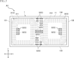
- FIG. 1 is a perspective view showing an electronic component according to a first embodiment
- FIG. FIG. 2 is a perspective view of FIG. 1 as seen through the sealing member.
- FIG. 3 is a plan view showing the electronic component according to the first embodiment;
- FIG. 4 is a plan view of FIG. 3 as seen through the sealing member.
- 5 is a plan view of FIG. 4 with the sealing member and the external electrodes omitted.
- FIG. 6 is a plan view of FIG. 5 with a part of the wiring portion (first wiring portion) omitted.
- 7 is a transparent view of a portion of the functional portion (inductor portion) and a portion of the wiring portion (second wiring portion) in the plan view of FIG.
- FIG. FIG. 15 is a cross-sectional view showing one step of the method for manufacturing the electronic component according to the first embodiment.
- FIG. 16 is a cross-sectional view showing one step of the method for manufacturing the electronic component according to the first embodiment.
- FIG. 17 is a cross-sectional view showing one step of the method for manufacturing the electronic component according to the first embodiment;
- FIG. 18 is a cross-sectional view showing one step of the method for manufacturing the electronic component according to the first embodiment;
- FIG. 19 is a cross-sectional view showing one step of the method for manufacturing the electronic component according to the first embodiment;
- FIG. 20 is a cross-sectional view showing one step of the method for manufacturing the electronic component according to the first embodiment.
- FIG. 21 is a cross-sectional view showing one step of the method for manufacturing the electronic component according to the first embodiment.
- FIG. 22 is a cross-sectional view showing one step of the method for manufacturing the electronic component according to the first embodiment
- FIG. 23 is a cross-sectional view showing one step of the method for manufacturing the electronic component according to the first embodiment
- FIG. 24 is a cross-sectional view showing an electronic component mounting structure according to the first embodiment
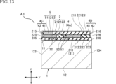
- 25 is a cross-sectional view showing the electronic component according to the second embodiment, and corresponds to the cross-section of FIG. 12.
- FIG. FIG. 26 is a cross-sectional view showing one step of the method for manufacturing an electronic component according to the second embodiment.
- FIG. 27 is a cross-sectional view showing one step of the method for manufacturing an electronic component according to the second embodiment.
- FIG. 28 is a perspective view showing an electronic component according to a third embodiment
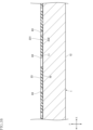
- FIG. 29 is a cross-sectional view showing the electronic component according to the fourth embodiment, corresponding to the cross-section of FIG. 12 .
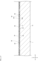
- FIG. 30 is a cross-sectional view showing the electronic component according to the fifth embodiment,
- a certain entity A is formed on a certain entity B
- a certain entity A is formed on (of) a certain entity B
- a certain thing A is formed in a certain thing B while another thing is interposed between a certain thing A and a certain thing B” including.
- ⁇ a certain entity A is placed on a certain entity B'' and ⁇ a certain entity A is placed on (of) a certain entity B'' mean ⁇ a certain entity A being placed directly on a certain thing B", and "a thing A being placed on a certain thing B with another thing interposed between something A and something B" include.
- ⁇ an object A is located on (of) an object B'' means ⁇ a certain object A is in contact with an object B, and an object A is located on an object B. Being located on (of)" and "something A is located on (something) B while another thing is interposed between something A and something B including "things”.
- ⁇ a certain object A overlaps an object B when viewed in a certain direction'' means ⁇ a certain object A overlaps all of an object B'', and ⁇ a certain object A overlaps an object B.'' It includes "overlapping a part of a certain thing B".
- ⁇ contains a certain material C (constituent material of a certain entity A)'' means ⁇ when (a constituent material of a certain entity A is composed of a certain material C)'' and ⁇ when a certain entity A (a constituent material of a certain entity A If the main component of is a certain material C, it includes ".
- First embodiment: 1 to 14 show an electronic component A1 according to the first embodiment.
- the electronic component A1 includes an insulating substrate 1, a sealing member 2, a functional portion 3, a plurality of external electrodes 4A to 4D, and a wiring portion 5.
- the thickness direction of the electronic component A1 will be referred to as "thickness direction z".
- thickness direction z one of the thickness directions z may be referred to as upward and the other as downward.
- descriptions such as “upper”, “lower”, “upper”, “lower”, “upper surface” and “lower surface” indicate the relative positional relationship of each component etc. in the thickness direction z, and are not necessarily It is not a term that defines the relationship with the direction of gravity.
- plane view refers to the time when viewed in the thickness direction z.
- a direction crossing the thickness direction z is referred to as a "first direction x".
- the first direction x is orthogonal to the thickness direction z.
- the first direction x is the horizontal direction in the plan view of the electronic component A1 (see FIGS. 2 to 7).
- a direction intersecting the thickness direction z and the first direction x is referred to as a “second direction y”.
- the second direction y is orthogonal to the thickness direction z and the first direction x.
- the second direction y is the vertical direction in the plan view of the electronic component A1 (see FIGS. 2 to 7).
- the insulating substrate 1 supports the sealing member 2 and the functional portion 3.
- the insulating substrate 1 is, for example, a semiconductor substrate.
- a constituent material of the semiconductor substrate includes, for example, Si (silicon).
- the insulating substrate 1 may be a glass substrate or a ceramic substrate instead of a semiconductor substrate.
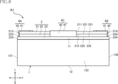
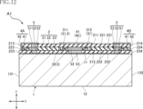
- the insulating substrate 1 has a substrate main surface 11, a substrate back surface 12 and a plurality of substrate side surfaces 131-134. As shown in FIGS. 8 to 14, the substrate main surface 11 and the substrate back surface 12 are separated from each other in the thickness direction z. The substrate main surface 11 faces upward in the thickness direction z, and the substrate back surface 12 faces downward in the thickness direction z. Each of the plurality of substrate side surfaces 131 to 134 is sandwiched between the substrate main surface 11 and the substrate back surface 12 in the thickness direction z. As shown in FIGS. 3 to 9 and 12, the pair of substrate side surfaces 131 and 132 are separated from each other in the first direction x and face opposite to each other in the first direction x. As shown in FIGS. 3 to 7, 10, 11, 13 and 14, the pair of substrate side surfaces 133 and 134 are separated from each other in the second direction y and are opposite to each other in the second direction y. turn to
- the sealing member 2 is arranged on the main surface 11 of the insulating substrate 1 .
- the sealing member 2 covers the functional portion 3 .
- the sealing member 2 includes a first insulating layer 21, a second insulating layer 22 and a third insulating layer .
- the first insulating layer 21, the second insulating layer 22 and the third insulating layer 23 are laminated in the thickness direction z.
- Each constituent material of the first insulating layer 21, the second insulating layer 22, and the third insulating layer 23 includes, for example, a photosensitive resin.
- the first insulating layer 21, the second insulating layer 22 and the third insulating layer 23 are made of dry film resist, for example.
- the first insulating layer 21 is laminated above the second insulating layer 22 in the thickness direction z.
- the first insulating layer 21 has a first main surface 211, a first back surface 212 and a plurality of first side surfaces 213-216.
- the first main surface 211 and the first back surface 212 are separated from each other in the thickness direction z.
- the first main surface 211 faces upward in the thickness direction z, and the first rear surface 212 faces downward in the thickness direction z.
- Each of the plurality of first side surfaces 213 to 216 is sandwiched between the first major surface 211 and the first back surface 212 in the thickness direction z.
- the pair of first side surfaces 213 and 214 are separated from each other in the first direction x and face opposite sides in the first direction x.
- the pair of first side surfaces 215 and 216 are separated from each other in the second direction y and face opposite sides in the second direction y.
- the second insulating layer 22 is laminated above the third insulating layer 23 in the thickness direction z.
- the second insulating layer 22 has a second main surface 221, a second back surface 222 and a plurality of second side surfaces 223-226.
- the second main surface 221 and the second back surface 222 are separated from each other in the thickness direction z.
- the second main surface 221 faces upward in the thickness direction z, and the second rear surface 222 faces downward in the thickness direction z.
- the second major surface 221 contacts the first rear surface 212 .
- the first insulating layer 21 is laminated on the second main surface 221 .
- Each of the plurality of second side surfaces 223 to 226 is sandwiched between the second main surface 221 and the second rear surface 222 in the thickness direction z.
- the pair of second side surfaces 223 and 224 are separated from each other in the first direction x and face opposite sides in the first direction x.
- the pair of second side surfaces 225 and 226 are separated from each other in the second direction y and face opposite sides in the second direction y.
- the plurality of second side surfaces 223-226 are flush with the plurality of first side surfaces 213-216, respectively.
- the third insulating layer 23 is laminated on the main surface 11 of the substrate. As shown in FIGS. 8-14, the third insulating layer 23 has a third main surface 231, a third back surface 232 and a plurality of third side surfaces 234-236. The third main surface 231 and the third rear surface 232 are separated from each other in the thickness direction z. The third main surface 231 faces upward in the thickness direction z, and the third rear surface 232 faces downward in the thickness direction z. The third main surface 231 contacts the second rear surface 222 . The second insulating layer 22 is laminated on the third major surface 231 .
- Each of the plurality of third side surfaces 233 to 236 is sandwiched between the third main surface 231 and the third rear surface 232 in the thickness direction z.
- the pair of third side surfaces 233 and 234 are separated from each other in the first direction x and face opposite sides in the first direction x.
- the pair of third side surfaces 235 and 236 are separated from each other in the second direction y and face opposite sides in the second direction y.
- the plurality of third side surfaces 233-236 are flush with the plurality of substrate side surfaces 131-134, respectively.
- the plurality of third side surfaces 233 to 236 are positioned outward from the plurality of second side surfaces 223 to 226, respectively.
- the third insulating layer 23 protrudes on both sides in the first direction x and both sides in the second direction y with respect to each of the first insulating layer 21 and the second insulating layer 22 .
- the plurality of third side surfaces 233-236 may be flush with the plurality of second side surfaces 223-226, respectively.
- the functional unit 3 is the electrical functional center of the electronic component A1.
- Functional portion 3 includes an inductor portion 31 and a capacitor portion 32 .
- Inductor section 31 and capacitor section 32 are electrically connected to form, for example, an LC filter.
- the LC filter may be a low-pass filter, a high-pass filter, or a band-pass filter (band-stop filter).
- the functional unit 3 is not limited to one that configures an LC filter with the inductor unit 31 and the capacitor unit 32 .
- inductor section 31 and capacitor section 32 may constitute a balanced-unbalanced conversion circuit called a balun.
- the inductor section 31 and the capacitor section 32 do not have to be electrically connected to each other inside the electronic component A1.
- the inductor section 31 is formed on the second insulating layer 22 .
- Inductor section 31 includes two winding sections 311 and 312 .
- the inductor section 31 is not limited to the example including the two winding portions 311 and 312, and may include one winding portion, or may include three or more winding portions.
- Each constituent material of the plurality of winding portions 311 and 312 includes a conductive material. This conductive material is, but is not limited to, copper or a copper alloy, for example.
- the current flowing through each winding 311, 312 provides inductance.
- Each of the two winding portions 311 and 312 is planarly wound on the second insulating layer 22 .
- the number of turns of each of the two windings 311, 312 is not limited to the illustrated example.
- the two winding portions 311 and 312 are arranged in the first direction x and electrically connected to each other via the wiring portion 5 .
- the inductor section 31 is not limited to the one formed in the second insulating layer 22, and is formed over two adjacent layers of the first insulating layer 21, the second insulating layer 22, and the third insulating layer 23 in the thickness direction z. may be formed.
- the capacitor section 32 is formed between the insulating substrate 1 and the third insulating layer 23 and sandwiched between them in the thickness direction z.
- Capacitor section 32 has, for example, an MIM (Metal-Insulator-Metal) structure.
- the capacitor section 32 is laminated in the order of metal layer-insulator-metal layer in the thickness direction z, and one or more capacitors are formed by the shape (arrangement pattern) of the two metal layers. there is This gives the capacitance.
- the capacitor section 32 is rectangular in plan view, but may be divided into a plurality of regions. The configuration of the capacitor section 32 is appropriately changed according to the type of filter required.
- Each of the plurality of external electrodes 4A to 4D is electrically connected to the functional section 3 (either or both of the inductor section 31 and the capacitor section 32).
- the external electrode 4A is electrically connected to one of the two winding portions 311 of the inductor portion 31 .
- the external electrode 4 ⁇ /b>B conducts to the other of the two winding portions 311 of the inductor portion 31 .
- the external electrodes 4A and 4B are electrically connected to the capacitor section 32, respectively.
- the two external electrodes 4C and 4D are electrically connected to the capacitor section 32, respectively.
- Each constituent material of the plurality of external electrodes 4A to 4D includes a conductive material. This conductive material is, but is not limited to, copper or a copper alloy, for example.
- each of the plurality of external electrodes 4A to 4D includes a main surface covering portion 41 and a side surface covering portion .
- the main surface covering portion 41 and the side surface covering portion 42 described below are common to the external electrodes 4A to 4D unless otherwise specified.
- the main surface covering portion 41 is formed on the first main surface 211 and covers a part of the first main surface 211 .
- the side surface covering portion 42 extends downward in the thickness direction z from the main surface covering portion 41 .
- the side surface covering portion 42 of the external electrode 4A extends from the first side surface 213 to the second side surface 223 and covers a portion of the first side surface 213 and a portion of the second side surface 223 .
- the side surface covering portion 42 of the external electrode 4B extends from the first side surface 214 to the second side surface 224 and covers part of the first side surface 214 and part of the second side surface 224 .
- the side surface covering portion 42 of the external electrode 4C extends from the first side surface 215 to the second side surface 225 and covers a portion of the first side surface 215 and a portion of the second side surface 225 .
- the side covering portion 42 of the external electrode 4 ⁇ /b>D extends from the first side 216 to the second side 226 and covers part of the first side 216 and part of the second side 226 .
- both or one of the surface (exposed surface) of the main surface covering portion 41 and the surface (exposed surface) of the side surface covering portion 42 is plated.
- This plating may be, for example, a multilayer structure in which a nickel layer, a palladium layer and a gold layer, or a nickel layer and a gold layer are laminated in order (from the surface of the main surface covering portion 41 and the side surface covering portion 42), A single layer structure such as a nickel layer or a gold layer may be used. Note that the plating does not have to be applied.
- the wiring portion 5 electrically connects the functional portion 3 and the plurality of external electrodes 4A to 4D.
- a constituent material of the wiring portion 5 includes a conductive material. This conductive material is, but is not limited to, copper or a copper alloy, for example.
- the wiring portion 5 includes a first wiring portion 51 , a second wiring portion 52 and a third wiring portion 53 .
- the first wiring portion 51 penetrates the first insulating layer 21 in the thickness direction z and is covered with the first insulating layer 21 .
- the second wiring portion 52 penetrates the second insulating layer 22 in the thickness direction z and is covered with the second insulating layer 22 .
- the third wiring portion 53 penetrates the third insulating layer 23 in the thickness direction z and is covered with the third insulating layer 23 .
- the portions where the first wiring portion 51, the second wiring portion 52, and the third wiring portion 53 overlap each other in plan view are the first wiring portion 51, the second wiring portion 52, and the third wiring. It has a tapered structure in the order of the portion 53 .
- the contact between the first wiring portion 51 and the second wiring portion 52 and the , the contact between the second wiring portion 52 and the third wiring portion 53 can be made more reliable.
- the portions where the first wiring portion 51, the second wiring portion 52, and the third wiring portion 53 overlap with each other in a plan view may have the same size.
- the second wiring portion 52, and the first wiring portion 51 are tapered in this order.
- each of the external electrodes 4A to 4D conducts to the functional section 3 (both or one of the inductor section 31 and the capacitor section 32) as follows.
- the external electrode 4A is electrically connected to the winding portion 311 (inductor portion 31) through the first wiring portion 51 and the second wiring portion 52, and It is electrically connected to the capacitor section 32 via the wiring section 51 , the second wiring section 52 and the third wiring section 53 .
- FIGS. 4 to 7 and 12 the external electrode 4A is electrically connected to the winding portion 311 (inductor portion 31) through the first wiring portion 51 and the second wiring portion 52, and It is electrically connected to the capacitor section 32 via the wiring section 51 , the second wiring section 52 and the third wiring section 53 .
- the external electrode 4B is electrically connected to the winding portion 312 (inductor portion 31) through the first wiring portion 51 and the second wiring portion 52, and It is electrically connected to the capacitor section 32 via the wiring section 51 , the second wiring section 52 and the third wiring section 53 .
- the two winding portions 311 and 312 are electrically connected to each other via the second wiring portion 52 .
- the external electrode 4C is electrically connected to the capacitor section 32 via the first wiring section 51, the second wiring section 52 and the third wiring section 53, as shown in FIG.
- the external electrode 4D is electrically connected to the capacitor section 32 via the first wiring section 51, the second wiring section 52 and the third wiring section 53.
- FIG. 15 to 23 are cross-sectional views showing one step of the method of manufacturing the electronic component A1, and correspond to the cross-section of the electronic component A1 shown in FIG.
- the method of manufacturing the electronic component A1 includes, for example, a substrate preparation step, a capacitor portion forming step, a primary insulating layer forming step, a primary wiring portion forming step, a secondary insulating layer forming step, a secondary wiring portion forming step, and a tertiary insulating layer forming step. , a resist forming process, a tertiary wiring portion forming process, an external electrode forming process, and a singulation process.
- Insulating substrate 1 to be prepared is, for example, a semiconductor substrate.
- a Si wafer is used as the semiconductor substrate.
- the insulating substrate 1 to be prepared may be a glass substrate instead of a semiconductor substrate, or may be a ceramic substrate.
- the capacitor section 32 to be formed has, for example, an MIM structure.
- the primary insulating layer forming step is a third insulating layer forming step for forming the third insulating layer 23 .
- a dry film resist is attached to the surface of the insulating substrate 1 on which the capacitor portion 32 is formed (substrate main surface 11).
- the dry film resist contains an epoxy resin as a photosensitive resin.
- the dry film resist is patterned by exposing and developing the applied dry film resist.
- the third insulating layer 23 having the pattern 83 is formed.
- the formed pattern 83 penetrates the third insulating layer 23 in the thickness direction z.
- the pattern 83 corresponds to the area where the third wiring portion 53 is arranged.
- the primary wiring portion forming step is a third wiring portion forming step for forming the third wiring portion 53 .
- the pattern 83 formed by the primary insulating layer forming step is filled with copper plating.
- a seed layer is formed by sputtering and/or vapor deposition on the upper surface of third insulating layer 23 having pattern 83 formed thereon, and then a mask having a predetermined pattern is formed.
- copper plating is formed by electroplating using a seed layer.
- the seed layer has a laminated structure of, for example, a titanium layer and a copper layer. After electroplating, the unnecessary mask and unnecessary seed layers are removed. Note that the filling method of the copper plating is not limited to this. Thereby, the third wiring portion 53 is formed.
- the secondary insulating layer forming step is a second insulating layer forming step for forming the second insulating layer 22 .
- a dry film resist is applied on the third insulating layer 23 .
- This dry film resist contains an epoxy resin as a photosensitive resin, as in the primary insulating layer forming step.
- the dry film resist is patterned by exposing and developing the applied dry film resist.
- the second insulating layer 22 having patterns 821 and 822 is formed.
- the formed patterns 821 and 822 penetrate the second insulating layer 22 in the thickness direction z.
- the pattern 821 corresponds to the region where the inductor portion 31 (two winding portions 311 and 312) is arranged, and the pattern 822 corresponds to the region where the second wiring portion 52 is arranged.
- the secondary wiring portion forming step is a second wiring portion forming step for forming the second wiring portion 52 .
- the patterns 821 and 822 formed by the secondary insulating layer forming step are filled with copper plating.
- the copper plating filled in the pattern 821 forms the inductor portion 31 (the two winding portions 311 and 312 ), and the copper plating formed in the pattern 822 forms the second wiring portion 52 .
- Filling with copper plating is carried out, for example, in the same manner as in the primary wiring portion forming step, by forming a seed layer and electroplating.
- the copper plating filling method in the secondary wiring portion forming step and the inductor portion forming step is not limited to this.
- the second wiring portion 52 and the inductor portion 31 are collectively formed.
- the primary wiring portion forming step, the secondary wiring portion forming step, and the inductor portion forming step may be performed collectively.
- the tertiary insulating layer forming step is a first insulating layer forming step for forming the first insulating layer 21 .
- a dry film resist is applied on the second insulating layer 22 .
- This dry film resist contains an epoxy resin as a photosensitive resin, as in the primary insulating layer forming step and the secondary insulating layer forming step.
- the dry film resist is patterned by exposing and developing the applied dry film resist.
- the first insulating layer 21 having the pattern 81 is formed.
- the formed pattern 81 penetrates the first insulating layer 21 in the thickness direction z.
- the pattern 81 corresponds to the area where the first wiring portion 51 is arranged.
- Resist formation process Next, as shown in FIG. 21, a resist 89 is formed. Resist 89 is formed by photolithography, for example. From the formed resist 89, a part of each end surface (each surface parallel to the thickness direction z) of the first insulating layer 21 and the second insulating layer 22 and a part of the upper surface of the first insulating layer 21 (thickness A part of each of the surfaces facing upwards in the direction z) is exposed.
- the tertiary wiring portion forming step is a first wiring portion forming step for forming the first wiring portion 51 .
- the pattern 81 formed by the tertiary insulating layer forming step and the portion exposed from the resist 89 are filled with copper plating.
- a first wiring portion 51 is formed by copper plating formed by the pattern 81, and a plurality of external electrodes 4A to 4D are formed in portions exposed from the resist 89. As shown in FIG.
- Filling with copper plating is carried out, for example, in the same manner as in the primary wiring portion forming step, by forming a seed layer and electroplating.
- the filling method of the copper plating in the tertiary wiring portion forming step and the external electrode forming step is not limited to this.
- the first wiring portion 51 and the plurality of external electrodes 4A to 4D are collectively formed.
- the resist 89 is removed.
- the exposed surfaces of the external electrodes 4A to 4D may be plated by electroless plating, for example.
- the insulating substrate 1 and the like are cut along cutting lines CL.
- the cutting method is not limited at all, for example, blade dicing or laser dicing is used. Thereby, the insulating substrate 1 is divided. Through the above steps, the electronic component A1 shown in FIGS. 1 to 14 is manufactured.
- FIG. 24 shows a state in which the electronic component A1 is mounted on a circuit board 90 as a mounting target.
- the electronic component A1 is bonded to the circuit board 90 in the thickness direction z opposite to the orientation shown in FIGS. Therefore, the main surface covering portion 41 of each of the external electrodes 4A to 4D faces the circuit board 90.
- Each of the external electrodes 4A-4D is joined to a circuit board 90 via a conductive joining material 91.
- Conductive bonding material 91 is, for example, solder.
- the conductive bonding material 91 adheres not only to the main surface covering portion 41 but also to the side surface covering portion 42 of the external electrode 4A.
- the fact that the conductive bonding material 91 adheres to the side covering portion 42 in this way also applies to the other external electrodes 4B to 4D.
- the electronic component A1 includes external electrodes 4A (4B to 4D) electrically connected to the functional portion 3.
- the external electrodes 4A (4B-4D) include main surface covering portions 41 covering the first main surface 211 and side surface covering portions 42 covering the first side surfaces 213 (214-216).
- the bonding area of the conductive bonding material 91 to the external electrodes 4A (4B to 4D) is further increased. Therefore, the electronic component A1 can increase the bonding strength to the mounting target. Furthermore, as understood from FIG.
- a portion of the conductive bonding material 91 is formed outward from the electronic component A1 in plan view.
- the state of adhesion of the conductive bonding material 91 to the external electrodes 4A (4B to 4D) can be easily visually observed. Since it is possible to confirm whether or not the conductive bonding material 91 is properly formed by such visual observation, it is possible to determine whether or not the bonding state is defective.
- the inventors of the present application simulated von Mises stress when a load is applied from the side of the electronic component in a configuration in which the external electrodes 4A (4B to 4D) include and do not include the side covering portions .
- the configuration in which the external electrodes 4A (4B to 4D) include the side covering portions 42 alleviates the von Mises stress more than the configuration in which the side covering portions 42 are not included.
- the electronic component A1 is provided with the side covering portions 42 on the external electrodes 4A (4B to 4D), thereby relieving the stress applied to the electronic component and improving the stability of the bonding state. From the above, it can be seen that the electronic component A1, by providing the side surface covering portions 42 on the external electrodes 4A (4B to 4D), can achieve a better bonding state to the mounted object than when the side surface covering portions 42 are not provided. It becomes possible. Further, according to the manufacturing method of the present disclosure, it is possible to manufacture the electronic component A1 capable of improving the bonding state with respect to the mounting target.
- the sealing member 2 includes the first insulating layer 21, the second insulating layer 22 and the third insulating layer 23, and the inductor section 31 is formed on the second insulating layer 22. According to this configuration, even if the inductor section 31 penetrates the second insulating layer 22 in the thickness direction z, unintentional conduction with other portions is suppressed. Therefore, according to the electronic component A1, it is possible to increase the Q value by increasing the dimension of the inductor section 31 in the thickness direction z, while suppressing unintended conduction of the inductor section 31 .
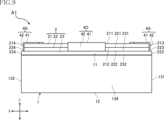
- FIG. 25 shows an electronic component A2 according to the second embodiment.
- the electronic component A2 differs from the electronic component A1 in the following points. That is, as understood from FIG. 25, the plurality of first side surfaces 213 to 216 of the first insulating layer 21 are located inwardly of the plurality of second side surfaces 223 to 226 of the second insulating layer 22 in plan view. Located in
- steps are generated between the plurality of first side surfaces 213 to 216 of the first insulating layer 21 and the plurality of second side surfaces 223 to 226 of the second insulating layer 22 due to the above configuration. ing. Therefore, steps are also generated in the side covering portions 42 of the plurality of external electrodes 4A to 4D.
- the manufacturing method of electronic component A2 differs from the manufacturing method of electronic component A1 in the following points. That is, the secondary wiring portion forming step and the inductor portion forming step are different from the resist forming step.
- 26 and 27 show one step of the method of manufacturing the electronic component A2.
- FIG. 26 is a cross-sectional view showing a secondary wiring portion forming step and an inductor portion forming step in the method of manufacturing the electronic component A2.
- FIG. 27 is a cross-sectional view showing a resist forming step, a tertiary wiring portion forming step, and an external electrode forming step in the method of manufacturing the electronic component A2.
- a resist 89 is formed so that at least part of the partial covering portion 421 is exposed. Then, a step can be formed in the side covering portion 42 by performing the same processing as the tertiary wiring portion forming step and the external electrode forming step in the manufacturing method of the electronic component A1.
- the external electrodes 4A (4B to 4D) include the side covering portions 42, so that the bonding state to the mounting object is better than when the side covering portions 42 are not included. becomes possible. Furthermore, in the electronic component A2, since the side covering portions 42 of the external electrodes 4A to 4D have steps, fillets are easily formed in the conductive bonding material 91 when the electronic component A2 is mounted on the circuit board 90. FIG. Therefore, according to the electronic component A2, it becomes easier to visually check the appearance.
- FIG. 28 shows an electronic component A3 according to the third embodiment.
- the electronic component A3 differs from the electronic component A1 in that dimples 43 are formed on each of the external electrodes 4A to 4D.
- the dimples 43 are semicircular depressions in plan view.
- the electronic component A3 has a shape of a photosensitive resin (dry film resist) in the primary to tertiary insulating layer forming process, and a shape of each resist (for example, resists 89 and 891) in the primary to tertiary wiring part forming process and the resist forming process. It is formed by appropriately changing and additionally arranging.
- the external electrodes 4A (4B to 4D) include the side covering portions 42, so that the bonding state to the mounting object is improved compared to the case where the side covering portions 42 are not included. becomes possible.
- the dimples 43 of the electronic component A3 facilitate the formation of fillets in the conductive bonding material 91 when the electronic component A3 is mounted on the circuit board 90. FIG. Therefore, according to the electronic component A3, like the electronic component A2, it becomes easier to visually check the appearance.
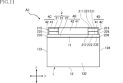
- FIG. 29 shows an electronic component A4 according to the fourth embodiment.
- the electronic component A4 differs from the electronic component A1 in that the sealing member 2 is composed of a single layer of the first insulating layer 21 .
- the inductor section 31 is formed on the first insulating layer 21 as shown in FIG.
- the inductor portion 31 does not penetrate the first insulating layer 21 in the thickness direction z. Thereby, unintended conduction between the inductor section 31 and the capacitor section 32 can be suppressed.
- the dimension of the inductor portion 31 in the thickness direction z is reduced, and the Q value of the inductor portion 31 may be lowered.
- the sealing member 2 includes a plurality of insulating layers and the inductor section 31 preferably penetrates the insulating layer in which the inductor section 31 is formed. Note that, unlike the illustrated example, the inductor portion 31 may penetrate through the first insulating layer 21 in the thickness direction z.
- the external electrodes 4A (4B to 4D) include the side covering portions 42, so that the bonding state to the mounting object is better than when the side covering portions 42 are not included. becomes possible.
- the number of insulating layers of the sealing member 2 is not limited at all. It should be noted that if the number of insulating layers is large, the thickness (dimension in the thickness direction z) of the electronic component of the present disclosure increases, which can increase the thickness of the electronic component. Therefore, the number of insulating layers of the sealing member 2 is preferably about 3 to 7 in order to suppress the enlargement of the electronic component.
- FIG. 30 shows an electronic component A5 according to the fifth embodiment.
- the electronic component A5 differs from the electronic component A1 in that the insulating substrate 1 is not provided.
- the electronic component A5 has the insulating substrate 1 removed, for example, by grinding the insulating substrate 1 in the manufacturing process.
- the thickness of the insulating substrate 1 (dimension in the thickness direction z) may be reduced by grinding the insulating substrate 1 instead of removing the insulating substrate 1 .
- the external electrodes 4A (4B to 4D) include the side covering portions 42, so that the bonding state to the mounting object is improved compared to the case where the side covering portions 42 are not included. becomes possible. Furthermore, since the electronic component A5 does not include the insulating substrate 1, it is preferable to achieve a slim design.
- the functional portion 3 of each electronic component A1 to A5 includes both the inductor portion 31 and the capacitor portion 32. However, only one of the inductor portion 31 and the capacitor portion 32 is provided. It may be a configuration including. Further, the functional portion 3 of each electronic component A1 to A5 may include inductors, capacitors, transistors, resistors, diodes, or the like singly or in combination.
- the electronic component and the manufacturing method thereof according to the present disclosure are not limited to the above-described embodiments.
- the specific configuration of each part of the electronic component of the present disclosure and the specific processing of each step of the method of manufacturing the electronic component of the present disclosure are subject to various design changes.
- the present disclosure includes embodiments set forth in the following appendices.
- Appendix 1. a functional part; a first insulating layer having a first main surface facing one of the thickness directions and a first side surface facing one of the first directions intersecting the thickness direction; an external electrode electrically connected to the functional unit; a wiring portion electrically connecting the functional portion and the external electrode; with The electronic component, wherein the external electrode includes a main surface covering portion covering the first main surface and a side surface covering portion covering the first side surface.
- Appendix 3. a second insulating layer having a second main surface facing one of the thickness directions and a second side surface facing one of the first directions; a third insulating layer having a third main surface facing one of the thickness directions; The first insulating layer is laminated on the second main surface,
- Appendix 4. 3.
- Appendix 5. The electronic component according to appendix 3 or appendix 4, wherein the side surface covering portion extends from the first side surface to the second side surface.
- Appendix 7. The electronic component according to any one of Appendixes 3 to 6, wherein the functional portion includes a capacitor portion.
- Appendix 8. It further comprises an insulating substrate, The insulating substrate has a main surface facing one of the thickness directions, 8.
- Appendix 9. The electronic component according to appendix 8, wherein the capacitor section is sandwiched between the insulating substrate and the third insulating layer in the thickness direction.
- a functional portion forming step of forming a functional portion a functional portion; a first insulating layer forming step of forming a first insulating layer having a first main surface facing one of the thickness directions and a first side surface facing one of the first directions intersecting the thickness direction; a wiring portion forming step of forming a wiring portion; an external electrode forming step of forming an external electrode including a main surface covering portion covering the first main surface and a side surface covering portion covering the first side surface; including The wiring section includes a first wiring section formed on the first insulating layer, each of the side surface covering portion and the first wiring portion is connected to the main surface covering portion; A method of manufacturing an electronic component, wherein the main surface covering portion, the side surface covering portion and the first wiring portion are collectively formed in the wiring portion forming step and the external electrode forming step.
- Appendix 11 further comprising a substrate preparation step of preparing an insulating substrate having a substrate main surface facing one of the thickness directions; 11. The method of manufacturing an electronic component according to Appendix 10, wherein the functional portion, the first insulating layer and the wiring portion are arranged on the main surface of the substrate.
- Appendix 12. a second insulating layer forming step of forming a second insulating layer having a second main surface facing one of the thickness directions; a third insulating layer forming step of forming a third insulating layer having a third main surface facing one of the thickness directions; In the second insulating layer forming step, the second insulating layer is laminated on the third main surface, 12.
- the wiring portion forming step includes a first wiring portion forming step of forming the first wiring portion, 13.
- the method of manufacturing an electronic component according to Appendix 12 wherein the first wiring portion penetrates the first insulating layer in the thickness direction.
- the wiring portion forming step includes a second wiring portion forming step of forming a second wiring portion penetrating the second insulating layer in the thickness direction, 14.
- the functional unit includes an inductor unit, 15.
- the wiring portion forming step includes a third wiring portion forming step of forming a third wiring portion penetrating the third insulating layer in the thickness direction, 16.
- the method of manufacturing an electronic component according to Appendix 14 or 15, wherein the second wiring portion and the third wiring portion are electrically connected to each other.
- Appendix 17. 17 The method of manufacturing an electronic component according to any one of Appendixes 12 to 16, wherein the first insulating layer, the second insulating layer, and the third insulating layer are formed of a dry film resist.
- A1 to A5 Electronic component 1: Insulating substrate 11: Main surface of substrate 12: Rear surface of substrate 131 to 134: Side surface of substrate 2: Sealing member 21: First insulating layer 211: First main surface 212: First rear surface 213 to 216 : first side surface 22: second insulating layer 221: second main surface 222: second back surface 223 to 226: second side surface 23: third insulating layer 231: third main surface 232: third back surface 233 to 236: third 3 side surface 3: functional portion 31: inductor portions 311, 312: winding portion 32: capacitor portions 4A to 4D: external electrodes 41: main surface covering portion 42: side surface covering portion 421: partial covering portion 43: dimple 5: wiring portion 51: First wiring part 52: Second wiring part 53: Third wiring part 81, 821, 822, 83: Patterns 89, 891: Resist 90: Circuit board 91: Conductive bonding material
Landscapes
- Engineering & Computer Science (AREA)
- Power Engineering (AREA)
- Microelectronics & Electronic Packaging (AREA)
- Manufacturing & Machinery (AREA)
- Coils Or Transformers For Communication (AREA)
Priority Applications (4)
| Application Number | Priority Date | Filing Date | Title |
|---|---|---|---|
| CN202280089958.5A CN118591851A (zh) | 2022-01-28 | 2022-12-26 | 电子部件和电子部件的制造方法 |
| DE112022006189.8T DE112022006189T5 (de) | 2022-01-28 | 2022-12-26 | Elektronische komponente und verfahren zum herstellen einer elektronischen komponente |
| JP2023576723A JPWO2023145365A1 (https=) | 2022-01-28 | 2022-12-26 | |
| US18/781,390 US20240379290A1 (en) | 2022-01-28 | 2024-07-23 | Electronic component and method for manufacturing electronic component |
Applications Claiming Priority (2)
| Application Number | Priority Date | Filing Date | Title |
|---|---|---|---|
| JP2022-012344 | 2022-01-28 | ||
| JP2022012344 | 2022-01-28 |
Related Child Applications (1)
| Application Number | Title | Priority Date | Filing Date |
|---|---|---|---|
| US18/781,390 Continuation US20240379290A1 (en) | 2022-01-28 | 2024-07-23 | Electronic component and method for manufacturing electronic component |
Publications (1)
| Publication Number | Publication Date |
|---|---|
| WO2023145365A1 true WO2023145365A1 (ja) | 2023-08-03 |
Family
ID=87471160
Family Applications (1)
| Application Number | Title | Priority Date | Filing Date |
|---|---|---|---|
| PCT/JP2022/047990 Ceased WO2023145365A1 (ja) | 2022-01-28 | 2022-12-26 | 電子部品および電子部品の製造方法 |
Country Status (5)
| Country | Link |
|---|---|
| US (1) | US20240379290A1 (https=) |
| JP (1) | JPWO2023145365A1 (https=) |
| CN (1) | CN118591851A (https=) |
| DE (1) | DE112022006189T5 (https=) |
| WO (1) | WO2023145365A1 (https=) |
Citations (2)
| Publication number | Priority date | Publication date | Assignee | Title |
|---|---|---|---|---|
| JP2011044614A (ja) * | 2009-08-21 | 2011-03-03 | Tdk Corp | 電子部品及びその製造方法 |
| JP2020205342A (ja) * | 2019-06-17 | 2020-12-24 | ローム株式会社 | チップ部品 |
-
2022
- 2022-12-26 JP JP2023576723A patent/JPWO2023145365A1/ja active Pending
- 2022-12-26 WO PCT/JP2022/047990 patent/WO2023145365A1/ja not_active Ceased
- 2022-12-26 DE DE112022006189.8T patent/DE112022006189T5/de active Pending
- 2022-12-26 CN CN202280089958.5A patent/CN118591851A/zh active Pending
-
2024
- 2024-07-23 US US18/781,390 patent/US20240379290A1/en active Pending
Patent Citations (2)
| Publication number | Priority date | Publication date | Assignee | Title |
|---|---|---|---|---|
| JP2011044614A (ja) * | 2009-08-21 | 2011-03-03 | Tdk Corp | 電子部品及びその製造方法 |
| JP2020205342A (ja) * | 2019-06-17 | 2020-12-24 | ローム株式会社 | チップ部品 |
Also Published As
| Publication number | Publication date |
|---|---|
| JPWO2023145365A1 (https=) | 2023-08-03 |
| CN118591851A (zh) | 2024-09-03 |
| US20240379290A1 (en) | 2024-11-14 |
| DE112022006189T5 (de) | 2024-10-02 |
Similar Documents
| Publication | Publication Date | Title |
|---|---|---|
| TWI309963B (en) | Semiconductor package, method of production of same, and semiconductor device | |
| TWI311904B (https=) | ||
| JP5333680B2 (ja) | 部品内蔵基板およびその製造方法 | |
| JP5234521B2 (ja) | 電子部品及びその製造方法 | |
| CN115720677A (zh) | 薄膜电容器及具备其的电子电路基板 | |
| JP2020145475A (ja) | 薄膜型lc部品およびその実装構造 | |
| CN112992504A (zh) | 电子部件 | |
| US10426032B1 (en) | Multilayer wiring structure and its manufacturing method | |
| JP2015181155A (ja) | 半導体装置および半導体装置の製造方法 | |
| JP2017228585A (ja) | 配線基板およびその製造方法、ならびに半導体装置の製造方法 | |
| JP5958454B2 (ja) | 部品内蔵モジュール | |
| JP7269755B2 (ja) | 電子装置および電子装置の製造方法 | |
| US11335614B2 (en) | Electric component embedded structure | |
| JP6819894B2 (ja) | 電子部品 | |
| WO2023145365A1 (ja) | 電子部品および電子部品の製造方法 | |
| JP5589617B2 (ja) | 薄膜コンデンサ及びその製造方法 | |
| US9117693B2 (en) | Passive integrated circuit | |
| JP2023114638A (ja) | 平衡不平衡変換素子 | |
| JPWO2019044857A1 (ja) | 配線基板、部品実装配線基板、半導体装置および配線基板の製造方法 | |
| JP2003124430A (ja) | 集積回路装置および集積回路用コンデンサ | |
| CN119153232B (zh) | 电容芯片结构以及制造方法 | |
| JP5846187B2 (ja) | 部品内蔵モジュール | |
| WO2023181917A1 (ja) | 電子部品の製造方法 | |
| JP7430988B2 (ja) | 電子装置 | |
| JP2020043249A (ja) | 多層配線構造体、部品実装多層配線構造体、多層配線基板、および部品実装多層配線基板 |
Legal Events
| Date | Code | Title | Description |
|---|---|---|---|
| 121 | Ep: the epo has been informed by wipo that ep was designated in this application |
Ref document number: 22924212 Country of ref document: EP Kind code of ref document: A1 |
|
| WWE | Wipo information: entry into national phase |
Ref document number: 2023576723 Country of ref document: JP |
|
| WWE | Wipo information: entry into national phase |
Ref document number: 202280089958.5 Country of ref document: CN |
|
| 122 | Ep: pct application non-entry in european phase |
Ref document number: 22924212 Country of ref document: EP Kind code of ref document: A1 |