WO2023145110A1 - コンデンサ - Google Patents
コンデンサ Download PDFInfo
- Publication number
- WO2023145110A1 WO2023145110A1 PCT/JP2022/031059 JP2022031059W WO2023145110A1 WO 2023145110 A1 WO2023145110 A1 WO 2023145110A1 JP 2022031059 W JP2022031059 W JP 2022031059W WO 2023145110 A1 WO2023145110 A1 WO 2023145110A1
- Authority
- WO
- WIPO (PCT)
- Prior art keywords
- conductor
- forming portion
- capacitance forming
- main surface
- capacitor
- Prior art date
- Legal status (The legal status is an assumption and is not a legal conclusion. Google has not performed a legal analysis and makes no representation as to the accuracy of the status listed.)
- Ceased
Links
Images














Classifications
-
- H—ELECTRICITY
- H01—ELECTRIC ELEMENTS
- H01G—CAPACITORS; CAPACITORS, RECTIFIERS, DETECTORS, SWITCHING DEVICES, LIGHT-SENSITIVE OR TEMPERATURE-SENSITIVE DEVICES OF THE ELECTROLYTIC TYPE
- H01G4/00—Fixed capacitors; Processes of their manufacture
- H01G4/002—Details
- H01G4/228—Terminals
-
- H—ELECTRICITY
- H01—ELECTRIC ELEMENTS
- H01G—CAPACITORS; CAPACITORS, RECTIFIERS, DETECTORS, SWITCHING DEVICES, LIGHT-SENSITIVE OR TEMPERATURE-SENSITIVE DEVICES OF THE ELECTROLYTIC TYPE
- H01G2/00—Details of capacitors not covered by a single one of groups H01G4/00-H01G11/00
- H01G2/02—Mountings
- H01G2/06—Mountings specially adapted for mounting on a printed-circuit support
-
- H—ELECTRICITY
- H01—ELECTRIC ELEMENTS
- H01G—CAPACITORS; CAPACITORS, RECTIFIERS, DETECTORS, SWITCHING DEVICES, LIGHT-SENSITIVE OR TEMPERATURE-SENSITIVE DEVICES OF THE ELECTROLYTIC TYPE
- H01G4/00—Fixed capacitors; Processes of their manufacture
- H01G4/30—Stacked capacitors
-
- H—ELECTRICITY
- H01—ELECTRIC ELEMENTS
- H01G—CAPACITORS; CAPACITORS, RECTIFIERS, DETECTORS, SWITCHING DEVICES, LIGHT-SENSITIVE OR TEMPERATURE-SENSITIVE DEVICES OF THE ELECTROLYTIC TYPE
- H01G4/00—Fixed capacitors; Processes of their manufacture
- H01G4/33—Thin- or thick-film capacitors (thin- or thick-film circuits; capacitors without a potential-jump or surface barrier specially adapted for integrated circuits, details thereof, multistep manufacturing processes therefor)
Definitions
- the present invention relates to a capacitor comprising a capacitance forming portion composed of a metal porous body, a dielectric film and a conductive film.
- a capacitor is formed by a metal porous body, a dielectric film covering the surface of the metal porous body, and a conductive film covering the dielectric film.
- a capacitor is disclosed comprising a portion.
- the metal porous body is composed of a sintered body of metal particles, and the dielectric layer and the conductive film are both formed by an atomic layer deposition (ALD) method.
- ALD atomic layer deposition
- the capacitor disclosed in Patent Document 1 has a structure in which the insulating substrate and the capacitor forming portion are bonded with a relatively large area, the thermal expansion coefficients of the insulating substrate and the capacitor forming portion are reduced during the manufacturing process involving heat treatment. The stress generated by the difference causes the capacitor itself to warp, which may hinder stable mounting of the capacitor.
- the present invention has been made to solve the above-described problems, and provides a capacitor having a capacitance forming portion composed of a metal porous body, a dielectric film, and a conductive film.
- the purpose is to improve the quality of
- a capacitor based on the present invention includes an insulating substrate, a capacitance forming portion, a first external connection wiring and a second external connection wiring.
- the insulating substrate has a first main surface and a second main surface opposite to the first main surface, and the capacitance forming portion is provided to face the first main surface. ing.
- the first external connection wiring and the second external connection wiring are connected to the capacitance formation section.
- the capacitance forming section includes a conductive porous metal body connected to the first external connection wiring, a dielectric film covering the surface of the metal porous body, and the second external connection wiring covering the dielectric film. and a conductive film connected to.
- the capacitance forming portion protrudes from the first main surface toward the capacitance forming portion, is surrounded by the capacitance forming portion, and is joined to the capacitance forming portion.
- a supporting portion for supporting is provided on the insulating substrate.
- the first external connection wiring may have a supporting conductor that constitutes the supporting portion. preferably connected.
- the first external connection wiring has a first via conductor penetrating through the insulating substrate so as to reach from the first main surface to the second main surface. good too.
- the support conductor may extend along the normal direction of the first main surface.
- the supporting conductor may be connected to the first via conductor by at least partially overlapping the supporting conductor with the first via conductor.
- the capacitance forming portion may include a first capacitance forming portion and a second capacitance forming portion stacked separately from each other in the normal direction of the first main surface.
- the metal porous body of the first capacitor forming portion and the metal porous body of the second capacitor forming portion are connected by the support conductor.
- the second external connection wiring includes a columnar conductor projecting from the first main surface toward the capacitance forming portion and surrounded by the capacitance forming portion; A second via conductor penetrating the insulating substrate to reach the second main surface from the main surface may further be provided.
- the conductive film and the second via conductor may be connected at least through the columnar conductor, and the columnar conductor extends along the normal direction of the first main surface. May be extended.
- the columnar conductor may overlap at least a part of the second via conductor when viewed along the normal direction of the first main surface.
- the capacitance forming portion may include a first capacitance forming portion and a second capacitance forming portion stacked separately from each other in the normal direction of the first main surface. good.
- the metal porous body of the first capacitance forming portion and the metal porous body of the second capacitance forming portion are connected by the support conductor.
- the conductive film of the first capacitance forming portion and the conductive film of the second capacitance forming portion are connected via at least the columnar conductor.
- the outer surface is provided on the first main surface, seals the capacitance forming portion, and is located on the opposite side of the insulating substrate when viewed from the capacitance forming portion. It may further include a sealing portion that defines the .
- the supporting conductor may be exposed on the outer surface by penetrating the capacitance forming portion and the sealing portion, and the columnar conductor may extend through the capacitance forming portion and the sealing portion. The columnar conductor may be exposed on the outer surface by passing through the sealing portion.
- the first via conductor and the second via conductor are both provided with the capacitance forming portion. It is preferably provided in the region where the
- a plurality of the first via conductors and the supporting conductors may be provided, and a plurality of the second via conductors and the columnar conductors may be provided.
- the first via conductors and the second via conductors may be arranged in an array when viewed along the normal direction of the first main surface, In that case, the polarity of one via conductor is preferably different from the polarity of the via conductor adjacent to it at the shortest distance.
- the first external connection wiring has a first via conductor penetrating through the insulating substrate so as to reach from the first main surface to the second main surface. good too.
- the support conductor may extend along the normal direction of the first main surface. In this case, the supporting conductor does not have to overlap the first via conductor.
- the capacitance forming portion may include a first capacitance forming portion and a second capacitance forming portion stacked separately from each other in the normal direction of the first main surface.
- the metal porous body of the first capacitor forming portion and the metal porous body of the second capacitor forming portion are connected by the support conductor.
- the supporting conductor contains the same material as at least part of the materials contained in the metal porous body.
- mounting stability and post-mounting reliability can be improved in a capacitor comprising a capacitance forming portion composed of a metal porous body, a dielectric film, and a conductive film.
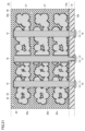
- FIG. 1 is a schematic front view of a capacitor according to Embodiment 1;
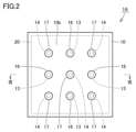
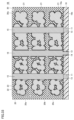
- FIG. FIG. 2 is a schematic bottom view of the capacitor shown in FIG. 1;
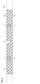
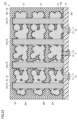
- FIG. 2 is a schematic cross-sectional view of the capacitor shown in FIG. 1;
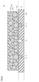
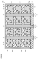
- 4 is a schematic cross-sectional view enlarging the vicinity of the first main surface of the insulating substrate shown in FIG. 3;
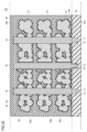
- FIG. 4 is an enlarged schematic cross-sectional view of the vicinity of a second via conductor shown in FIG. 3;
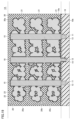
- FIG. 4 is a schematic cross-sectional view enlarging a part of the sealing portion shown in FIG. 3;
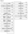
- FIG. 2 is a flowchart showing a method of manufacturing a capacitor according to Embodiment 1; 8 is a schematic cross-sectional view showing a state after step S4 of the manufacturing flow shown in FIG. 7 is completed;
- FIG. FIG. 8 is a schematic cross-sectional view for explaining step S5 of the manufacturing flow shown in FIG. 7;
- FIG. 8 is a schematic cross-sectional view for explaining step S6 of the manufacturing flow shown in FIG. 7;
- FIG. 8 is a schematic cross-sectional view for explaining step S7 of the manufacturing flow shown in FIG. 7;
- FIG. 8 is a schematic cross-sectional view for explaining step S8 of the manufacturing flow shown in FIG. 7;
- FIG. 8 is a schematic cross-sectional view for explaining step S9 of the manufacturing flow shown in FIG.
- FIG. 8 is a schematic cross-sectional view for explaining step S10 of the manufacturing flow shown in FIG. 7;
- FIG. 8 is a schematic cross-sectional view for explaining step S11 of the manufacturing flow shown in FIG. 7;
- FIG. 8 is a schematic cross-sectional view for explaining step S12 of the manufacturing flow shown in FIG. 7;
- FIG. 8 is a schematic cross-sectional view for explaining step S13 of the manufacturing flow shown in FIG. 7;
- FIG. 8 is a schematic cross-sectional view for explaining step S14 of the manufacturing flow shown in FIG. 7;
- FIG. 8 is a schematic cross-sectional view for explaining step S15 of the manufacturing flow shown in FIG. 7;
- FIG. 8 is a schematic cross-sectional view for explaining step S16 of the manufacturing flow shown in FIG.
- FIG. 7 is a schematic cross-sectional view for explaining step S17 of the manufacturing flow shown in FIG. 7;
- 4 is a schematic cross-sectional view showing one form of a columnar conductor in the capacitor shown in FIG. 3.
- FIG. FIG. 5 is a schematic cross-sectional view of a capacitor according to a first modified example;
- FIG. 11 is a schematic cross-sectional view of a capacitor according to a second modified example;
- FIG. 11 is a schematic cross-sectional view of a capacitor according to a third modified example;
- FIG. 11 is a schematic cross-sectional view of a capacitor according to a fourth modified example;
- FIG. 10 is a schematic cross-sectional view of a capacitor according to Embodiment 2;
- FIG. 10 is a flowchart showing a method of manufacturing a capacitor according to Embodiment 2;
- FIG. 29 is a schematic cross-sectional view for explaining step S7 of the manufacturing flow shown in FIG. 28;
- FIG. 29 is a schematic cross-sectional view for explaining step S9 of the manufacturing flow shown in FIG. 28;
- 29 is a schematic cross-sectional view for explaining step S14B of the manufacturing flow shown in FIG. 28;
- FIG. FIG. 29 is a schematic cross-sectional view for explaining step S15 of the manufacturing flow shown in FIG. 28;
- FIG. 29 is a schematic cross-sectional view for explaining step S16 of the manufacturing flow shown in FIG. 28;
- FIG. 29 is a schematic cross-sectional view for explaining step S7 of the manufacturing flow shown in FIG. 28;
- FIG. 29 is a schematic cross-sectional view for explaining step S9 of the manufacturing flow shown in FIG. 28;
- 29 is a schematic cross-sectional view for explaining step S14B of the manufacturing flow shown in
- FIG. 11 is a schematic cross-sectional view of a capacitor according to Embodiment 4;
- FIG. 11 is a flowchart showing a method for manufacturing a capacitor according to Embodiment 4;
- FIG. 1 is a schematic front view of the capacitor according to Embodiment 1
- FIG. 2 is a schematic bottom view of the capacitor viewed in the direction of arrow II shown in FIG. 3 is a schematic cross-sectional view of the capacitor along line III-III shown in FIG. 2
- FIG. 4 is a schematic cross-sectional view enlarging the vicinity of the first main surface of the insulating substrate shown in FIG. 5 is a schematic cross-sectional view enlarging the vicinity of the second via conductor shown in FIG. 3, and
- FIG. 6 is a schematic cross-sectional view enlarging a part of the sealing portion shown in FIG.
- the capacitor 1A is a so-called surface-mounted electronic component having a flat, substantially rectangular parallelepiped outer shape and a bottom surface configured as a mounting surface for a wiring board or the like.
- Capacitor 1A mainly includes insulating substrate 10 , capacitance forming portion 20 , and sealing portion 30 .
- the capacitance forming portion 20 is provided so as to face the insulating substrate 10 .
- Capacitance forming portion 20 is located inside capacitor 1A by being sealed by insulating substrate 10 and sealing portion 30 provided on insulating substrate 10 .
- the insulating substrate 10 is provided with first via conductors 13 and second via conductors 14 , support conductors 15 , first bumps 16 and second bumps 17 , and columnar conductors 18 .
- These first via conductors 13, second via conductors 14, support conductors 15, first bumps 16, second bumps 17, and columnar conductors 18 electrically connect capacitance forming portion 20 located inside capacitor 1A to an external circuit.
- a pair of external connection wirings are configured as lead wirings for direct connection.
- the pair of external connection wirings includes a first external connection wiring as an anode and a second external connection wiring as a cathode.
- the insulating substrate 10 is a flat member having a first principal surface 10a and a second principal surface 10b opposite to the first principal surface 10a.
- the insulating substrate 10 it is preferable to use a substrate having electrical insulating properties, and preferably a substrate containing an inorganic material as a main component can be used. More specifically, the insulating substrate 10 is, for example, any one of Si, Al2O3 , ZrO2 , BN , Si3N4 , AlN, MgO, Mg2SiO4 , BaTiO3 , SrTiO3 and CaTiO3 . can be used as the main material.
- the thickness and size of the insulating substrate 10 are not particularly limited. preferably used.
- the insulating substrate 10 is provided with a plurality of first through holes 11.
- Each of the plurality of first through holes 11 extends from the first main surface 10a to the second main surface 10b. passes through.
- Each of the plurality of first through holes 11 is filled with a first via conductor 13 (see FIG. 3).
- Each of the plurality of first via conductors 13 has a substantially cylindrical shape, for example.
- a plurality of second through holes 12 are provided in the insulating substrate 10, and each of the plurality of second through holes 12 extends from the first main surface 10a to the second main surface 10b. passes through.
- Each of the plurality of second through holes 12 is filled with a second via conductor 14 (see FIG. 3).
- Each of the plurality of second via conductors 14 has a substantially cylindrical shape, for example.
- Each of the plurality of first via conductors 13 constitutes part of the above-described first external connection wiring.
- Each of the plurality of second via conductors 14 constitutes part of the above-described second external connection wiring. That is, the plurality of first via conductors 13 and the plurality of second via conductors 14 respectively constitute first external connection wirings and second external connection wirings having different polarities.
- both first via conductor 13 and second via conductor 14 are capacitance forming portion 20 when viewed along the normal direction of first main surface 10a of insulating substrate 10. is provided in the area (that is, the area indicated by the dashed line in FIG. 2).
- first via conductors 13 and five second via conductors 14 are provided on insulating substrate 10, so that a total of nine via conductors are provided on insulating substrate 10. passes through.
- These nine via conductors are arranged in an array with a layout of 3 rows and 3 columns.
- the polarity of one via conductor and the polarity of the via conductor adjacent to it at the shortest distance are different.
- the number and arrangement of the first via conductors 13 and the second via conductors 14 are not particularly limited to this.
- first via conductor 13 and the second via conductor 14 can be a metal material having particularly high electrical conductivity.
- the material of the first via conductor 13 and the second via conductor 14 can be a metal material mainly composed of Ni, Ag, Cu, Au, Pt, Mo, or W, for example. is preferred.
- the materials of the first via conductor 13 and the second via conductor 14 can be appropriately changed according to the mounting environment of the capacitor 1A according to the present embodiment.
- the material of the two via conductors 14 does not necessarily have to be the same.
- first via conductor 13 and second via conductor 14 are made of Ni.
- the second via conductors 14 may be formed together with the columnar conductors 18 described later by a thick film forming method such as electrolytic plating or screen printing.
- the material of the second via conductors 14 is the same as the material of the columnar conductors 18 to be described later.
- first via conductor 13 and the second via conductor 14 are not particularly limited, and are appropriately set according to the thickness and size of the insulating substrate 10 .
- first via conductor 13 and second via conductor 14 preferably have axial lengths of, for example, 5 ⁇ m or more and 50 ⁇ m or less, and preferably have diameters of, for example, 15 ⁇ m or more and 150 ⁇ m or less.
- the insulating substrate 10 is provided with a plurality of substantially columnar supporting conductors 15 that protrude from the first main surface 10a toward the capacitance forming portion 20 and are surrounded by the capacitance forming portion 20.
- the plurality of supporting conductors 15 configured in this way function as supporting portions that support the capacitance forming portion 20 by being joined to the capacitance forming portion 20 respectively. That is, by providing a plurality of supporting conductors 15 as these supporting portions, it is possible to suppress warping of the insulating substrate 10 due to stress generated in the manufacturing process of the capacitor 1A. will be described later.
- each of the plurality of supporting conductors 15 extends along the normal direction of the first main surface 10a, and overlaps each of the plurality of first via conductors 13 when viewed along the normal direction. are placed. Thereby, the support conductor 15 is connected to the first via conductor 13 .
- each of the plurality of supporting conductors 15 is preferably arranged so as to be substantially coaxial with each of the plurality of first via conductors 13 . Moreover, it is preferable that each of the plurality of supporting conductors 15 has a cross section perpendicular to the normal direction of the first main surface 10a larger than the cross section of the corresponding first via conductor 13 . Therefore, it is preferable that the diameter of each of the plurality of supporting conductors 15 is, for example, 15 ⁇ m or more and 100 ⁇ m or less.
- each of the conductors 15 can be arranged to at least partially overlap with each of the plurality of first via conductors 13 when viewed along the normal direction of the first main surface 10a. Therefore, by doing so, each of the plurality of supporting conductors 15 can be reliably connected to each of the plurality of first via conductors 13 .
- the axial length of the support conductor 15 is not particularly limited, and is appropriately set according to the thickness of the capacitance forming portion 20. However, it should be long enough to pass through the capacitance forming portion 20 in its thickness direction. It is preferable to have As will be described later, in the case where the capacitance forming portion 20 includes a plurality of laminated capacitance forming portions spaced apart from each other in the normal direction of the first main surface 10a, the capacitor forming portion 20 that is the farthest from the first main surface 10a It must have an axial length sufficient to be bonded to at least a portion of the layer located on the bottom (that is, the first capacitance forming portion 20a in FIG. 3).
- the axial length of the plurality of supporting conductors 15 preferably has a lower limit of, for example, 15 ⁇ m and an upper limit of a length obtained by subtracting 20 ⁇ m from the thickness of the capacitor 1A.
- the supporting conductor 15 preferably contains the same material as at least a part of the materials contained in the metal porous body 21 to be described later.
- the material of the support conductor 15 can be a metal material mainly composed of, for example, any one of Ni, Mo, W, Al, Ti, Ta, Nb, Cu, Pt, Au and Ag.
- the support conductor 15 may be made of an alloy material containing two or more selected from these metal materials as main components.
- the supporting conductor 15 is made of Ni.
- the outer shape of the support conductor 15 when viewed from above is not limited to a substantially circular shape, and may be, for example, a substantially elliptical shape. Further, the support conductor 15 may extend in a direction tapered considerably with respect to the normal direction of the first main surface 10a.
- the insulating substrate 10 is further provided with a plurality of substantially cylindrical columnar conductors 18 protruding from the first main surface 10 a toward the capacitance forming section 20 and surrounded by the capacitance forming section 20 .
- Each of the plurality of columnar conductors 18 extends along the normal direction of the first main surface 10a, and when viewed along the normal direction of the first main surface 10a, the plurality of second via conductors 14 placed on top of each other.
- the columnar conductor 18 is connected to the second via conductor 14 at its end on the insulating substrate 10 side.
- each of the plurality of columnar conductors 18 is preferably arranged so as to be substantially coaxial with each of the plurality of second via conductors 14 .
- each of the plurality of columnar conductors 18 has a cross section orthogonal to the normal direction of the first main surface 10a larger than the corresponding cross section of the second via conductor 14 . Therefore, it is preferable that the diameter of each of the plurality of columnar conductors 18 is, for example, 15 ⁇ m or more and 150 ⁇ m or less.
- each of the conductors 18 can be arranged to at least partially overlap with each of the plurality of second via conductors 14 when viewed along the normal direction of the first main surface 10a. Therefore, by doing so, each of the plurality of columnar conductors 18 can be reliably connected to each of the plurality of second via conductors 14 .
- the axial length of the columnar conductor 18 is not particularly limited, and is appropriately set according to the thickness of the capacitance forming portion 20. It is preferable to have As will be described later, in the case where the capacitance forming portion 20 includes a plurality of laminated capacitance forming portions spaced apart from each other in the normal direction of the first main surface 10a, the capacitor forming portion 20 that is the farthest from the first main surface 10a It must have an axial length sufficient to be bonded to at least a portion of the layer located on the bottom (that is, the first capacitance forming portion 20a in FIG. 3).
- the axial length of the plurality of columnar conductors 18 preferably has a lower limit of, for example, 15 ⁇ m and an upper limit of a length obtained by subtracting 20 ⁇ m from the thickness of the capacitor 1A.
- the columnar conductor 18 preferably contains the same material as at least a part of the material contained in the metal porous body 21 to be described later.
- the material of the columnar conductors 18 can be a metal material mainly composed of, for example, any one of Ni, Mo, W, Al, Ti, Ta, Nb, Cu, Pt, Au and Ag.
- the columnar conductor 18 may be made of an alloy material containing two or more selected from these metal materials as main components.
- the columnar conductors 18 may be formed together with the second via conductors 14 by a thick film forming method such as electrolytic plating or screen printing. In that case, the material of the columnar conductors 18 is the same as the material of the second via conductors 14 . In the present embodiment, both second via conductors 14 and columnar conductors 18 made of Ni are formed by electroplating.
- the outer shape of the columnar conductor 18 when viewed from above is not limited to a substantially circular shape, and may be, for example, a substantially elliptical shape. Also, the columnar conductor 18 may extend in a direction substantially tapered with respect to the normal direction of the first main surface 10a.
- Each of the plurality of support conductors 15 described above constitutes part of the first external connection wiring described above, and each of the plurality of columnar conductors 18 constitutes part of the second external connection wiring described above. are doing. That is, the plurality of supporting conductors 15 and the plurality of columnar conductors 18 constitute first external connection wirings and second external connection wirings having different polarities, respectively.
- a plurality of first bumps 16 are provided on the second main surface 10 b of the insulating substrate 10 so as to cover the plurality of first via conductors 13 .
- the plurality of first bumps 16 serve as a bonding material for mounting the capacitor 1A as a surface-mounted electronic component on a wiring board or the like and electrically connecting the capacitance forming portion 20 of the capacitor 1A to an external circuit. and is provided so as to protrude from the second main surface 10 b of the insulating substrate 10 .
- Each of the plurality of first bumps 16 has a substantially semispherical shape.
- a plurality of second bumps 17 are provided on the second main surface 10 b of the insulating substrate 10 so as to cover the plurality of second via conductors 14 .
- the plurality of second bumps 17 serve as bonding materials for mounting the capacitor 1A as a surface-mounted electronic component on a wiring board or the like, and for electrically connecting the capacitance forming portion 20 of the capacitor 1A to an external circuit. and is provided so as to protrude from the second main surface 10 b of the insulating substrate 10 .
- Each of the plurality of second bumps 17 has a substantially semispherical shape.
- Each of the plurality of first bumps 16 constitutes part of the above-described first external connection wiring.
- Each of the plurality of second bumps 17 constitutes part of the above-described second external connection wiring. That is, the plurality of first bumps 16 and the plurality of second bumps 17 constitute first external connection wirings and second external connection wirings having different polarities, respectively.
- first bump 16 and the second bump 17 can be used for the first bump 16 and the second bump 17, but it is preferable to use a metal material having particularly high electrical conductivity.
- the material of the first bumps 16 and the material of the second bumps 17 can be metal materials, for example, Ni, Ag, Cu, Au, and Sn as main materials.
- first bump 16 and second bump 17 are made of Au.
- the sizes of the first bumps 16 and the second bumps 17 are not particularly limited, and are appropriately set according to the sizes of the first via conductors 13 and the second via conductors 14 .
- the first external connection wiring serving as the anode of the pair of external connection wirings is composed of the first via conductor 13, the support conductor 15, and the first bump 16.
- the second external connection wiring as the cathode of is composed of the second via conductor 14 , the columnar conductor 18 and the second bump 17 .
- the capacitance forming part 20 is provided to face the insulating substrate 10, and covers the porous metal body 21 having a plurality of fine holes inside and the surface of the porous metal body 21. It includes a dielectric film 22 and a conductive film 23 further covering the surface of the dielectric film 22 .
- the capacitance forming portion 20 is provided so as to face the insulating substrate 10, it is not substantially directly joined to the insulating substrate 10, or is assumed to be directly joined to the insulating substrate 10. are only slightly joined.
- the state in which the capacitance forming portion 20 is only slightly bonded to the insulating substrate 10 means a state in which a portion of the capacitance forming portion 20 is bonded to the insulating substrate 10 at a predetermined ratio or less. That is, the state in which the capacitance forming portion 20 is only slightly joined to the insulating substrate 10 means that the insulating substrate 10 is in a cross section perpendicular to the extending direction of the first main surface 10a of the insulating substrate 10, as shown in FIG.
- the metal porous body 21 is directly with respect to the insulating substrate 10, or via the dielectric film 22 or the conductive film 23
- the sum of the line segment lengths parallel to the first main surface 10a of the indirectly joined portion is the total line length in the arbitrary region of the first main surface. It means that it is 30% or less of the segment length (that is, the line segment length a in the example shown in FIG. 4).
- the capacitance forming portion 20 includes a plurality of capacitance forming portions stacked and separated from each other in the normal direction of the first main surface 10a.
- the number of layers of the laminated capacitance forming portion is not particularly limited, and is appropriately set according to the desired capacitance.
- Capacitance forming portion 20 in the present embodiment is composed of three layers.
- first capacitance forming portion 20a and second capacitance forming portion 20b will be referred to as a third capacitance forming portion 20c.
- At least part of the plurality of fine holes provided inside the metal porous body 21 are not closed by the metal porous body itself, and preferably the plurality of fine holes provided inside the metal porous body 21 are not closed. are not closed by the metal porous body itself.
- a metal porous body is composed of, for example, a sintered body of metal particles.
- the metal porous body 21 is positioned so as to surround the support conductor 15 on the portion of the first main surface 10a of the insulating substrate 10 excluding the edge portion.
- the metal porous body 21 configured in this manner is fired together with the support conductor 15 containing at least part of the same material as the material contained in the metal porous body 21 in the forming process.
- the metal porous body 21 is joined to the support conductor 15 . That is, in the capacitor 1A according to the present embodiment, the porous metal body 21 of the first capacitance forming portion 20a, the porous metal body 21 of the second capacitance forming portion 20b, and the porous metal body 21 of the third capacitance forming portion 20c are connected by the support conductor 15 . Therefore, the first external connection wiring as the anode described above is connected to the capacitance forming section 20 via the supporting conductor 15 .
- the metal porous body 21 can be composed of various conductive metal materials, but Ni, Mo, W, Al, Ti, Ta, Nb, Cu, Pt, Au and Ag are mainly used. It is preferable to configure this with a metal material as a material.
- the metal porous body 21 may be made of an alloy material containing two or more selected from these metal materials as main components. In this embodiment, the metal porous body 21 is made of Ni.
- the thickness and size of the metal porous body 21 are not particularly limited, and the size in particular is appropriately set according to the size of the insulating substrate 10 .
- the metal porous body 21 is preferably composed of a sintered body of metal particles.
- metal particles having various shapes such as spherical, ellipsoidal, flat, plate-like, and needle-like can be used.
- the particle size of the metal particles is not particularly limited, but the average particle size is preferably 600 nm or less, more preferably 20 nm or more and 500 nm or less.
- the dielectric film 22 covers the surface of the metal porous body 21 as described above. More specifically, the dielectric film 22 not only covers the surface of the metal porous body 21 in the outermost portion of the capacitance forming portion 20, but also covers the portion of the metal porous body 21 located inside the capacitance forming portion 20. Among the surfaces of the porous body 21, it also covers the surfaces defined by the above-described fine pores that are not closed by the metal porous body itself. The dielectric film 22 also covers the surface of the support conductor 15 .
- Dielectric film 22 can be composed of various insulating materials, such as AlO x , SiO x , HfO x , TiO x , TaO x , ZrO x , SiAlO x , HfAlO x , ZrAlO x .
- the dielectric film 22 is any one of AlOx (for example Al2O3 ), SiOx (for example SiO2 ), HfOx , TiOx , SiAlOx, HfAlOx , ZrAlOx , HfSiOx and ZrSiOx . is preferably constructed.
- the above chemical formula simply indicates the structure of the material, and does not limit the composition. That is, x, y and z attached to O and N may be arbitrary values greater than 0, and the abundance ratio of each element including metal elements is arbitrary.
- the dielectric film 22 may be composed of a laminated film composed of a plurality of dielectric layers made of different materials. In this embodiment, the dielectric film 22 is made of AlSiO.
- the dielectric film 22 is preferably formed by a vapor phase method, such as a vacuum deposition method, a chemical vapor deposition (CVD) method, a sputtering method, an atomic layer deposition (ALD) method, or a pulsed laser deposition (PLD) method. or by a method using a supercritical fluid, and particularly preferably by an ALD method.
- a vapor phase method such as a vacuum deposition method, a chemical vapor deposition (CVD) method, a sputtering method, an atomic layer deposition (ALD) method, or a pulsed laser deposition (PLD) method.
- the thickness of the dielectric film 22 is not particularly limited, it is preferably 3 nm or more and 100 nm or less, more preferably 5 nm or more and 50 nm or less.
- the conductive film 23 covers the surface of the dielectric film 22 as described above. More specifically, the conductive film 23 not only covers the surface of the dielectric film 22 in the outermost portion of the capacitance forming portion 20, but also covers the portion of the dielectric film 22 located inside the capacitance forming portion 20. It also covers the surface of membrane 22 . The conductive film 23 also covers the surface of the dielectric film 22 covering the surface of the support conductor 15 .
- the conductive film 23 is positioned so as to surround the plurality of columnar conductors 18 projecting from the first main surface 10a toward the capacitance forming portion 20 and is connected to the plurality of columnar conductors 18 . That is, in the capacitor 1A according to the present embodiment, the conductive film 23 of the first capacitance forming portion 20a, the conductive film 23 of the second capacitance forming portion 20b, and the conductive film 23 of the third capacitance forming portion 20c are They are connected via the columnar conductors 18 .
- the conductive film 23 can be made of various conductive materials, any one of Ni, Cu, Ru, Al, W, Ti, Ag, Au, Zn, Ta and Nb is used as the main material.
- metal materials alloy materials containing two or more selected from these metal materials as main components, metal nitrides such as TiN, TiAlN, TiSiN, TaN, NbN, and WN, metal oxynitrides such as TiON and TiAlON, Conductive polymers such as PEDOT (poly(3,4-ethylenedioxythiophene)), polypyrrole and polyanine, and conductive oxide films such as RuO 2 , ZnO, (Zn, Al) O and NiO. be able to. Among them, it is preferable to configure the conductive film 23 with an oxide semiconductor such as TiN, TiON, ZnO, or RuO. In this embodiment, the conductive film 23 is made of TiN.
- the conductive film 23 can be preferably formed by a CVD method, an ALD method, a PLD method, a plating method, a bias sputtering method, a sol-gel method, a method using conductive polymer filling, or a method using a supercritical fluid. , particularly preferably formed by the ALD method. Also, the conductive film 23 may be configured by a laminated film composed of a plurality of conductive layers made of different materials. In that case, the film can be formed by another method after the film is formed by the ALD method.
- the thickness of the conductive film 23 is not particularly limited, it is preferably 3 nm or more, more preferably 10 nm or more.
- the dielectric film 22 and the conductive film 23 described above cover not only the surface of the metal porous body 21 but also a predetermined portion of the insulating substrate 10 on the first main surface 10a side. Furthermore, as shown in FIG. 5, the dielectric film 22 and the conductive film 23 also cover the surface of the insulating substrate 10 in the portion defining the second through holes 12 provided in the insulating substrate 10 . More specifically, at the boundary between the second via conductor 14 and the base material of the insulating substrate 10, the base material of the insulating substrate 10 is covered with a dielectric film 22, and the dielectric film 22 is a conductive film. 23 , and the conductive film 23 is further covered with the second via conductor 14 .
- the conductive film 23 is directly connected to the second via conductor 14 and is also connected to the second via conductor 14 via the columnar conductor 18 . Therefore, the above-described second external connection wiring as a cathode is connected to the capacitance forming portion 20 via the second via conductor 14 or via the second via conductor 14 and the columnar conductor 18 .
- the sealing portion 30 is provided on the first main surface 10a of the insulating substrate 10, seals the capacitance forming portion 20 together with the insulating substrate 10, and seals the capacitance forming portion. It defines an outer surface 30a located on the side opposite to the insulating substrate 10 side when viewed from 20 . More specifically, the sealing portion 30 is positioned to cover the upper, lateral and lower portions of the capacitance forming portion 20 provided to face the first main surface 10a of the insulating substrate 10, and further are located so as to fill a hole provided inside the capacitance forming portion 20 .
- the sealing portion 30 can be made of various insulating materials, but is preferably made of an insulating material having excellent weather resistance.
- the material of the sealing portion 30 can be, for example, a resin material such as polyimide resin, polybenzoxazole resin, polyethylene terephthalate resin, benzocyclobutene resin, or epoxy resin.
- various additives can be included in the resin material, and for example, SiO 2 filler, Al 2 O 3 filler, etc. may be included in order to adjust the coefficient of thermal expansion.
- the sealing portion 30 is made of epoxy resin.
- a moisture-resistant protective film may be formed between the capacitance forming portion 20 and the sealing portion 30 .
- the moisture-resistant protective film is formed by applying an inorganic insulator made of SiN, SiO 2 , Al 2 O 3 , HfO 2 , ZrO 2 or the like to the capacitance forming portion 20 by CVD, ALD, or the like.
- a water-repellent organic insulator such as a fluorine-based resin or a silane coupling agent resin may be provided so as to cover the capacitance forming portion 20 .
- the moisture-resistant protective film does not necessarily have to be formed inside the capacitance forming portion 20, and it is sufficient if it is formed so as to cover only the outer surface.
- the sealing portion 30 can be formed by various coating methods, for example, a method using a vacuum laminator, a method using an air dispenser, a method using a jet dispenser, a screen printing method, a vacuum printing method, An electrostatic coating method, an inkjet method, a photolithography method, or the like can be used.
- the thickness and size of the sealing portion 30 are not particularly limited, and the size is appropriately set according to the size of the insulating substrate 10 .
- the thickness of the sealing portion 30 is preferably 5 ⁇ m or more and 50 ⁇ m or less, for example.
- the thickness of the sealing portion 30 described above is measured, for example, by observing a cross section orthogonal to the extending direction of the first main surface 10a of the insulating substrate 10 using an optical microscope.
- the longitudinal direction of the capacitor 1A is Lx
- the lateral direction is Ly
- the thickness direction of the capacitor 1A (that is, the normal direction of the first main surface 10a) is Lz
- the capacitor 1A is polished so that the Lx-Lz cross section of the capacitor 1A located in the center in the Ly direction is exposed.
- the polishing process is performed so that the exposed cross section is positioned within an error range of ⁇ 100 ⁇ m in the Ly direction with respect to the center position.
- the observation range of the cross section in the Lx direction is a range of ⁇ 50 ⁇ m from the center position of the cross section in the Lx direction, and is a range in which neither the support conductor 15 nor the columnar conductor 18 is provided.
- the thickness of the sealing portion 30 in the Lz direction is measured at 10 points at equal intervals in the Lx direction, and the average value of these measurements is calculated.
- the average value calculated in this manner is the thickness of the sealing portion 30 .
- three of the thicknesses in the Lz direction of the sealing portion 30 measured at these ten points are illustrated as line segment lengths e1, e2, and e3.
- the capacitance forming portion 20 composed of the metal porous body 21, the dielectric film 22 and the conductive film 23 is integrated with the insulating substrate 10 and the sealing portion 30. , and electrical extraction of the capacitance forming portion 20 is realized by a pair of external connection wirings.
- FIG. 7 is a flow diagram showing a method of manufacturing a capacitor according to this embodiment.
- 8 to 21 are schematic cross-sectional views for explaining each step of the manufacturing flow shown in FIG. 7, respectively.
- the manufacturing method of the capacitor 1A shown below manufactures an assembly of capacitors that are in the process of being processed by collectively processing up to the middle stage of the manufacturing process, and then separates the assembly by dividing the assembly. 2) is a method of simultaneously mass-producing a plurality of capacitors 1A by further processing the work-in-progress after singulation.
- a green sheet is produced in step S1. Specifically, Al 2 O 3 powder and glass powder are weighed, and these Al 2 O 3 powder and glass powder are mixed with an organic solvent such as toluene and ethanol, and a binder such as polyvinyl butyral. This mixture is then formed into a sheet, thereby producing a green sheet from which the insulating substrate is made. After the green sheets are produced, they are cut to prepare a plurality of green sheets.
- an organic solvent such as toluene and ethanol
- a binder such as polyvinyl butyral
- step S2 first through holes and second through holes are formed in some of the plurality of green sheets. Specifically, a first through-hole to be filled later by a first via conductor that is a part of the anode is provided at a predetermined position of the green sheet, and a second via conductor that is a part of the cathode is provided at a predetermined position of the green sheet. A second through hole is provided which is to be filled later.
- the method of forming the first through holes and the second through holes is not particularly limited, but for example, the first through holes and the second through holes are formed by irradiating the green sheet with laser light. can do.
- the first through-holes and the second through-holes may be formed by processing using a mechanical puncher or sandblasting.
- step S3 first via conductors are formed in the green sheet in which the first through holes and the second through holes are formed. Specifically, a conductive paste is applied to the green sheet so as to fill the first through holes. At that time, the second through holes should not be filled with the conductive paste.
- the method of applying the conductive paste is not particularly limited, but for example, a screen printing method can be used.
- the green sheet is fired in step S4. Specifically, a green sheet having no first through-holes and second through-holes is superimposed on the green sheet to which the conductive paste has been applied in step S3, and the superimposed green sheets are pressure-bonded. be done. Then, the laminate of green sheets after pressure bonding is degreased, and then the laminate of green sheets after degreasing is fired.
- the first through hole and the second through hole are not provided on the other main surface of the green sheet coated with the conductive paste, which faces the one main surface.
- Green sheets are laminated.
- a uniaxial press machine for example, can be used for crimping the green sheets.
- the firing of the green sheet is performed at a temperature of 700° C. to 1000° C. in an air atmosphere, for example.
- the insulating substrate is a so-called multiple substrate in which insulating substrates to be finally included in each of a plurality of capacitors are connected in a matrix. Only the substrate 10 will be noted, and the surrounding portion thereof is omitted from the dashed lines.
- the first through hole and the second through hole are formed in step S2, and then the first via conductor is formed in step S3.
- the second through hole may be formed after the first via conductor is formed.
- the case where the green sheet and the conductive paste are fired at the same time is described as an example.
- a second through hole may be provided.
- the insulating substrate after baking is provided with first through holes and second through holes by, for example, sandblasting, wet etching, or dry etching, and then a conductive paste is applied to form the first and second through holes. It should be baked.
- the first via conductor may be formed by sputtering, vapor deposition, plating, or the like.
- a conductive paste layer for forming the metal porous body 21 is applied. More specifically, as shown in FIG. 9, a conductive paste layer 21p is applied on the first main surface 10a of the insulating substrate 10 for forming the metal porous body 21, which will be described later.
- the second through holes 12 provided in the insulating substrate 10 are coated with an epoxy resin or the like (not shown). It is preferable that a closing portion that closes the second through hole 12 is provided. This is to prevent the conductive paste from entering the inside of the second through hole 12 .
- conductive metal particles 21a and a binder 21b composed of an organic solvent such as terpineol and ethyl cellulose varnish are weighed and mixed, and a conductive paste is produced based on the mixture by using a rolling machine. .
- the conductive paste thus produced is applied onto the first main surface 10a of the insulating substrate 10 and dried so as to have a rectangular pattern shape as a whole when viewed from above.
- a conductive paste containing metal particles 21a made of Ni is used.
- the conductive paste is applied in multiple layers to form a layer having a predetermined thickness on the insulating substrate 10 .
- Each conductive paste applied on the insulating substrate 10 becomes the metal porous body 21 described above through a firing process described later.
- the layered conductive paste composed of the metal particles 21a and the binder 21b thus formed is referred to as a conductive paste layer 21p.
- step S6 a resin paste layer is applied. More specifically, as shown in FIG. 10, on the conductive paste layer 21p formed in a sheet shape on the first main surface 10a of the insulating substrate 10, a resin paste layer 21c is formed as a whole in plan view. It is applied in a rectangular shape and dried.
- the resin paste layer 21c separates a plurality of conductive paste layers 21p, which will be described later, and will disappear in the firing process, which will be described later.
- a resin paste layer 21c made of acrylic resin is used.
- step S7 a conductive paste layer and a resin paste layer are further laminated. More specifically, as shown in FIG. 11, conductive paste layer 21p and resin paste layer 21c are further formed on conductive paste layer 21p and resin paste layer 21c already applied on insulating substrate 10. They are laminated so as to be alternately arranged in the normal direction of the first main surface 10a. As a result, a laminate including a plurality of conductive paste layers 21p and resin paste layers 21c is formed on insulating substrate 10 .
- the laminate described above is composed of a total of three conductive paste layers 21p and a total of two resin paste layers 21c.
- the number of paste layers 21c is not particularly limited, and is appropriately set according to the desired capacity.
- the layer farthest from the first main surface 10a of the insulating substrate 10 is configured to be the conductive paste layer 21p. It may be configured to be a layer in which it lies.
- supporting conductor holes are formed in step S8. More specifically, as shown in FIG. 12, a portion of the laminate overlapping with the first via conductor 13 when viewed along the normal direction of the first main surface 10a is provided with a conductor piercing through the laminate. A plurality of supporting conductor holes 15h are formed. The plurality of supporting conductor holes 15h are to be filled with supporting conductors in the step of forming the supporting conductors, which will be described later. Further, in the present embodiment, the cross section of each of the plurality of supporting conductor holes 15 h is configured to be larger than the cross section of each of the first via conductors 13 .
- the method for forming the supporting conductor hole 15h is not particularly limited, but for example, the supporting conductor hole 15h can be formed by irradiating the laminate with a laser beam. Alternatively, the supporting conductor holes 15h may be formed by processing using a mechanical puncher or sandblasting.
- a supporting conductor is formed in step S9. More specifically, as shown in FIG. 13, the supporting conductor holes 15h are filled with the conductive paste so as to fill the supporting conductor holes 15h.
- the plurality of supporting conductors 15 formed in this manner protrude from the first main surface 10a toward the laminate and are surrounded by the laminate. Further, each of the plurality of supporting conductors 15 thus formed is connected to each of the plurality of first via conductors 13 .
- Ni paste is used as the conductive paste embedded in the supporting conductor holes 15h.
- the support conductor 15 containing the same material as the material contained in the metal particles 21a that is, the material contained in the metal porous body 21
- the supporting conductor 15 and the porous metal body 21 are firmly metal-bonded.
- the method of applying the conductive paste to be embedded in the supporting conductor holes 15h is not particularly limited, but for example, a screen printing method can be used.
- step S10 columnar conductor holes are formed in step S10. More specifically, as shown in FIG. 14, a portion of the laminate overlapping the second through-hole 12 when viewed along the normal direction of the first main surface 10a is provided with a A plurality of columnar conductor holes 18 h are formed to reach the second through holes 12 .
- the plurality of columnar conductor holes 18h are to be filled with columnar conductors in a columnar conductor formation process described later. Further, in the present embodiment, the cross section of each of the plurality of columnar conductor holes 18 h is configured to be larger than the cross section of each of the second through holes 12 .
- the method of forming the columnar conductor holes 18h is not particularly limited, but for example, the columnar conductor holes 18h can be formed by irradiating the laminate with laser light. Alternatively, the columnar conductor holes 18h may be formed by processing using a mechanical puncher or sandblasting.
- step S11 the laminate and the supporting conductor are fired. More specifically, as shown in FIG. 15, the laminate and the support conductor 15 are fired, thereby sintering the adjacent metal particles 21a contained in the conductive paste layer 21p to metal-join. At the same time, the metal particles 21a and the supporting conductors 15 adjacent to the metal particles 21a are joined. In addition, the resin paste layer 21c included in the laminate disappears due to the heat during the firing, thereby forming a plurality of metal porous bodies laminated apart from each other in the normal direction of the first main surface 10a. 21 will be formed.
- the insulating substrate 10 Prior to performing the above-described firing, the insulating substrate 10 is degreased, and then the above-described laminate is obtained at a temperature of 400° C. to 900° C. in a reducing atmosphere of a mixture of nitrogen and hydrogen, for example. and firing of the support conductor 15 is performed.
- the atmosphere during firing is preferably a reducing atmosphere as described above, but can be set to an atmosphere below the equilibrium oxygen partial pressure of the metal selected as the main component of the metal particles 21a.
- the support conductor 15 contains Ni, which is the same material as the material contained in the metal particles 21a in the conductive paste layer 21p.
- the metal particles 21a and the support conductor 15 are sintered by the above-described firing to form a metal joint. Mechanical strength will be improved.
- the insulating substrate 10 would be unacceptably warped due to the heat load during firing as described above.
- the support conductor 15 described above is provided in order to suppress the warpage, but this point will be described later.
- a dielectric film is formed in step S12. More specifically, as shown in FIG. 16, the portion that covers the surfaces of the first main surface 10a, the metal porous body 21, and the supporting conductor 15 and defines the second through holes 12 provided in the insulating substrate 10 A dielectric film 22 is formed to cover the surface of the insulating substrate 10 of .
- the method of forming the dielectric film 22 is not particularly limited as described above, but the ALD method is preferably used. If the ALD method is used, the raw material of the dielectric film 22 can be supplied in the form of a gas, so it is possible to select the material and adjust the film thickness at the atomic layer level. Therefore, even if the fine pores provided inside the metal porous body 21 are extremely small, a homogeneous and dense dielectric film 22 can be formed. Further, by using the ALD method, it is possible to easily cover the surface of the insulating substrate 10 at the portion defining the second through hole 12 provided in the insulating substrate 10 with the dielectric film 22 .
- the dielectric film 22 is formed using this ALD method, a raw material is added to the fine holes provided inside the metal porous body 21 and the insides of the second through holes 12 provided in the insulating substrate 10 .
- a raw material gas that has high vapor pressure, is easy to gasify, has high thermal stability, and has high reactivity.
- TMA trimethylaluminum
- TDMAS trisdimethylaminosilane
- the dielectric film 22 is formed using the ALD method.
- the dielectric film 22 is formed under a temperature condition of, for example, 150° C. or more and 400° C. or less, although it differs depending on the film formation method and the film formation material. If all or most of the capacitance forming portion 20 is directly bonded to the insulating substrate 10, unacceptable warping of the insulating substrate 10 due to the heat load during the formation of the dielectric film 22 may occur.
- the support conductor 15 described above is provided in order to suppress the warpage, but this point will be described later.
- a conductive film is formed in step S13. More specifically, as shown in FIG. 17, conductive film 23 is formed to cover dielectric film 22 formed in step S12.
- the method of forming the conductive film 23 is not particularly limited as described above, but the ALD method is preferably used. If the ALD method is used, the raw material of the conductive film 23 can be supplied in the form of a gas, so it is possible to select the material and adjust the film thickness at the atomic layer level. Therefore, even if the fine pores provided inside the metal porous body 21 are extremely small, a homogeneous and dense conductive film 23 can be formed. Further, by using the ALD method, the dielectric film 22 provided inside the second through hole 12 of the insulating substrate 10 can also be easily covered with the conductive film 23 .
- the formation of the conductive film 23 is performed under temperature conditions of, for example, 200° C. or more and 600° C. or less, although this varies depending on the film formation method and the film formation material. If all or most of the capacitance forming portion 20 were directly bonded to the insulating substrate 10, the insulating substrate 10 would unacceptably warp due to the thermal load during the formation of the conductive film 23. As a result, in the present embodiment, the support conductor 15 described above is provided in order to suppress the warpage, but this point will be described later.
- the capacitance forming portion 20 is provided to face each other, and further includes a plurality of capacitance forming portions that are laminated while being separated from each other in the normal direction of the first main surface 10a.
- step S14 second via conductors and columnar conductors are formed. More specifically, as shown in FIG. 18, a plurality of second via conductors 14 and columnar conductors 18 are formed so as to fill the plurality of second through holes 12 and columnar conductor holes 18h provided in the insulating substrate 10. It is formed.
- the second via conductors 14 and the columnar conductors 18 may be formed by a thick film forming method such as electrolytic plating or screen printing.
- both second via conductors 14 and columnar conductors 18 made of Ni are formed by electroplating.
- the second via conductor 14 formed in this way is connected to the conductive film 23 covering its side surface.
- the plurality of columnar conductors 18 formed in this manner protrude from the first main surface 10a toward the capacitance forming portion 20, and are surrounded by the conductive film 23 of the capacitance forming portion 20 to be connected thereto. be. As a result, the plurality of columnar conductors 18 are connected to the capacitance forming section 20 via the conductive film 23 .
- the second via conductor 14 formed as described above is joined to the columnar conductor 18 at the end face of the second via conductor 14 on the capacitance forming portion 20 side.
- the second via conductor 14 is connected not only to the capacitance forming portion 20 via the conductive film 23 covering it, but also to the capacitance forming portion 20 via the columnar conductor 18 .
- a sealing portion is formed in step S15. More specifically, as shown in FIG. 19, a sealing portion 30 is provided on the first main surface 10a of the insulating substrate 10 on which the capacitance forming portion 20 is provided so as to cover the capacitance forming portion 20. .
- the sealing portion 30 is formed by so-called compression molding, for example. More specifically, first main surface 10a of insulating substrate 10 is covered with a resin sheet, and in this state, a vacuum laminator is used to evacuate first main surface 10a of insulating substrate 10. A resin sheet is brought into close contact. In this state, the resin sheet is heated to 50° C. to 100° C. to laminate the capacitance forming portion 20 , and then heated to 100° C. to 200° C. to perform main curing. A sealing portion 30 is formed. The method for forming the sealing portion 30 is not limited to the compression molding described above, and may be performed by so-called transfer molding.
- the capacitance forming portion 20 is sealed by the insulating substrate 10 and the sealing portion 30, preventing moisture from entering the capacitance forming portion 20 from the outside and ensuring moisture resistance. become.
- the capacitance forming portion 20 is covered with the sealing portion 30, and the capacitance forming portion 20 is physically protected by the sealing portion 30 as well.
- the curing conditions shown above are merely examples, and can be changed in various ways.
- step S16 the insulating substrate is ground. More specifically, as shown in FIG. 20, the second main surface 10b side of insulating substrate 10 located on the side opposite to the side on which capacitance forming portion 20 is provided is planarized.
- a grind tape (not shown) is attached to the capacitance forming portion 20 side, and the portion of the insulating substrate 10 that closes the first via conductor 13 and the second through hole 12 is planarly cut. will be removed respectively. As a result, the end of first via conductor 13 and the end of second via conductor 14 are exposed on the second main surface 10b side.
- step S17 first bumps and second bumps are formed on the insulating substrate. More specifically, as shown in FIG. 21 , first bumps are formed on second main surface 10 b of insulating substrate 10 so as to cover first via conductors 13 and second via conductors 14 provided on insulating substrate 10 . 16 and a second bump 17 are formed.
- the first bumps 16 and the second bumps 17 can be formed simultaneously by, for example, electrolytic plating.
- portions other than the vicinity of the portions where first via conductors 13 and second via conductors 14 are exposed are covered with an ultraviolet curable resin film as a mask (not shown), and electroplating is performed in this state to form the first bumps.
- 16 and the second bumps 17 can be formed to protrude from the second main surface 10b. After the electroplating is completed, the UV curable resin film as a mask is removed.
- the method for forming the second via conductor 14, the first bump 16, and the second bump 17 described above is not limited to the method using the electrolytic plating described above, but may also be a screen printing method using a conductive paste. , an inkjet method, a dispenser method, or the like, and a combination of baking can also be used.
- the conductive paste should contain a metal that can be fired at a low temperature and a sintering aid so that firing can be performed under temperature conditions that do not affect the resin forming the sealing portion 30. is preferred.
- step S18 the insulating substrate is singulated. More specifically, by dividing the insulating substrate 10, a plurality of capacitors 1A connected to each other are separated into individual pieces.
- a groove is formed in at least one of the insulating substrate 10 and the sealing portion 30, and a force is applied to the insulating substrate 10 and the sealing portion 30 so as to bend from the groove as a starting point.
- the insulating substrate 10 and the sealing portion 30 are broken.
- Diamond scribing, laser scribing, dicing, or the like can be used as a method for forming grooves.
- individualization may be performed by directly cutting the insulating substrate 10 and the sealing portion 30 by scribing or dicing.
- the capacitor 1A according to the first embodiment described above is manufactured.
- the grinding process is performed after the sealing part is formed has been exemplified. It is also possible to form Further, the singulation may be performed immediately after the grinding process is performed, or the grinding process may be performed immediately after the singulation process.
- the capacitance forming portion 20 is joined to each of the plurality of supporting conductors 15, on the other hand, as described above, it is connected to the insulating substrate 10. are substantially not directly bonded, or are only slightly bonded, if at all.
- the heat of the insulating substrate 10 and the capacitance forming portion 20 is reduced in the manufacturing process involving the heat treatment of the capacitor 1A (that is, the firing process, the process of forming the dielectric film 22, and the process of forming the conductive film 23).
- the stress generated due to the difference in expansion coefficients can be reduced.
- warping of the insulating substrate 10 due to the stress can be effectively suppressed, and the dielectric film 22 and the conductive film 23 from above the insulating substrate 10 caused by the warping of the insulating substrate 10 can be prevented. Peeling can also be effectively suppressed.
- the plurality of supporting conductors 15 protrude from the first main surface 10a toward the capacitance forming portion 20 and are surrounded by the capacitance forming portion 20. there is Thereby, each of the plurality of supporting conductors 15 is joined to the capacitance forming portion 20 .
- the insulating substrate and the capacitor may be damaged by the influence of heat applied from the outside and heat generated inside after mounting. Stress is generated due to the difference in the coefficient of thermal expansion of the forming portion, and the stress causes the capacitor 1A to warp and possibly damage the joint portion between the insulating substrate and the metal porous body. By using the capacitor 1A, it is possible to effectively suppress the occurrence of such a problem.
- the capacitor including the capacitance forming portion 20 composed of the metal porous body 21, the dielectric film 22, and the conductive film 23 is improved in mounting stability and post-mounting reliability. This will result in an improvement in quality.
- a capacitor is provided with a lead wiring in order to electrically connect a capacitance forming portion formed inside the capacitor to a circuit located outside the capacitor. It is important to increase the contact area between the capacitance forming portion and the lead-out wiring and to increase the cross-sectional area of the lead-out wiring perpendicular to the conducting direction.
- the first external connection wiring as the lead wiring includes the first via conductor 13 and the support conductor 15 provided on the insulating substrate 10.
- the metal porous body 21 of the capacitance forming portion 20 is connected to the first via conductor 13 via the supporting conductor 15 .
- the support conductor 15 is provided so as to protrude from the first main surface 10a toward the capacitance forming portion 20, and the contact area at the interface formed by the support conductor 15 and the metal porous body 21 provided in this way is is larger than the contact area at the interface formed by the metal porous body 21 directly connected to the first via conductor 13 . Therefore, by configuring in this way, the contact area at the interface formed by the metal porous body 21 and the support conductor 15 can be increased.
- the diameter of the support conductor 15 is as small as several tens of ⁇ m. Therefore, since the metal porous body 21 is connected to the first via conductor 13 via the supporting conductor 15 , the first via conductor 13 can be more easily connected than the case where the metal porous body 21 is directly connected to the first via conductor 13 . It is possible to increase the cross-sectional area of the external connection wiring perpendicular to the conducting direction.
- the second external connection wiring as the lead wiring includes the second via conductors 14 and the columnar conductors 18 provided on the insulating substrate 10.
- the conductive film 23 of the capacitance forming portion 20 is connected to the second via conductor 14 via the columnar conductor 18 .
- the columnar conductor 18 is provided so as to protrude from the first main surface 10a toward the capacitance forming portion 20, and the contact area at the interface formed by the columnar conductor 18 and the conductive film 23 thus provided is , the contact area at the interface formed by the conductive film 23 when the conductive film 23 is directly connected to the second via conductor 14 . Therefore, by configuring in this way, the contact area at the interface formed by the conductive film 23 and the columnar conductor 18 can be increased.
- the thickness of the conductive film 23 is about several hundred nanometers at the largest, while the diameter of the columnar conductor 18 is about several tens of micrometers at the smallest.
- the columnar conductor 18 is configured to have a larger cross-sectional area than the conductive film 23, thereby making it possible to increase the cross-sectional area of the second external connection wiring.
- the capacitor 1A it is possible to reduce the ESR in the capacitor including the capacitance forming portion 20 composed of the metal porous body 21, the dielectric film 22, and the conductive film 23. Obviously, by providing the capacitor 1A according to the present embodiment, it is possible to reduce the ESR in the capacitor including the capacitance forming portion 20 composed of the metal porous body 21, the dielectric film 22, and the conductive film 23. Obviously, by providing the capacitor 1A according to the present embodiment, it is possible to reduce the ESR in the capacitor including the capacitance forming portion 20 composed of the metal porous body 21, the dielectric film 22, and the conductive film 23. Become.
- capacitor 1A when viewed along the normal direction of first main surface 10a of insulating substrate 10, first via conductor 13 and second via All of the conductors 14 are provided within the region where the capacitance forming portion 20 is arranged (that is, the region indicated by the dashed line in FIG. 2).
- neither the first external connection wiring nor the second external connection wiring is arranged at a position on the side of the capacitance forming section 20 . It is possible to minimize the sealing portion 30 of the portion to be connected. Therefore, not only can the capacitor 1A be made smaller than the conventional one, but the volume occupied by the portion other than the capacitance forming portion 20 in the capacitor 1A is reduced, so that the capacity can be increased.
- first via conductor 13 and second via conductor 14 are positioned so as to pass through insulating substrate 10 in the thickness direction. They are arranged close to each other with their current paths directed in opposite directions. Therefore, the magnetic fields generated in these via conductors act so as to cancel each other out due to the flow of current, so that the so-called ESL (equivalent series inductance) can be reduced.
- ESL equivalent series inductance
- the first via conductors 13 and the second via conductors 14 are arranged in an array, and the polarity of one via conductor and this The polarities of via conductors adjacent to each other at the shortest distance are different from each other. By configuring in this way, the effect of reducing the ESL described above can be maximized.
- each of the pair of external connection wirings for electrically drawing out capacitance forming portion 20 is configured to include a plurality of via conductors. It is With this configuration, the cross-sectional area of the current path can be increased compared to the case where each of the pair of external connection wirings is composed of a single via conductor, so that the ESR can be reduced. Become.
- the base material of the insulating substrate 10 is covered by the dielectric film 22 at the boundary between the second via conductor 14 and the base material of the insulating substrate 10.
- dielectric film 22 is covered with conductive film 23
- conductive film 23 is further covered with second via conductor 14 .
- the adhesion between the base material of the insulating substrate 10 and the second via conductors 14 is improved compared to the case where the base material of the insulating substrate 10 and the second via conductors 14 are directly bonded. As a result, it is possible to suppress the intrusion of moisture through this portion. Therefore, the capacitor can have excellent moisture resistance.
- the metal porous body 21 is composed of a sintered body of metal particles.
- the metal particles are metal-bonded to each other, thereby improving the mechanical strength of the capacitance forming portion 20 and increasing the bonding area between the metal particles, so that the ESR can be reduced. be able to. Furthermore, it is possible to obtain the effect that a metal porous body having open pores can be formed relatively easily.
- FIG. 22 is a schematic cross-sectional view showing one form of a columnar conductor related to the capacitor shown in FIG.
- the columnar conductor 18 is located on the insulating substrate 10 side when viewed from the capacitance forming portion 20 of the pair of ends of the columnar conductor 18, as shown in FIG.
- the end located on the opposite side is formed in a hollow shape, and the sealing portion 30 may be formed by entering this hollow portion. Even in the capacitor 1A' including the columnar conductors 18 formed in this manner, the effects described above can be obtained.
- FIG. 23 is a schematic cross-sectional view of a capacitor according to a first modified example.
- capacitor 1A1 according to the first modification based on the first embodiment described above will be described.
- the capacitor 1A1 according to the first modification differs from the capacitor 1A according to the first embodiment described above in the position where the support conductor 15 is formed and the configuration of the second external connection wiring. ing.
- each of the plurality of supporting conductors 15a corresponds to the first via conductor. 13 and second via conductor 14.
- the supporting conductor formed at a position overlapping neither the first via conductor 13 nor the second via conductor 14 is formed at a position overlapping the first via conductor 13 .
- the number of supporting conductors 15a is not particularly limited, and is appropriately set according to the size of the insulating substrate 10 or desired capacity.
- the columnar conductor 18 is not formed, and the second external connection wiring is composed only of the second via conductors 14 and the second bumps 17.
- the support conductor 15a is not directly joined to the first via conductor 13. Therefore, the first via conductor 13 is electrically connected to the porous metal body 21 of the third capacitor forming part 20c by joining at least a part of the end face on the side of the capacitor forming part 20 to the porous metal body 21 of the third capacitor forming part 20c. It is In addition, the metal porous bodies 21 of the plurality of laminated capacitor forming portions are connected to each other via the support conductors 15a that are joined to all of them.
- the dielectric film 22 and the conductive film 23 cover the surface of the insulating substrate 10 in the portion defining the second through holes 12 provided in the insulating substrate 10.
- the base material of the insulating substrate 10 is covered with a dielectric film 22, and the dielectric film 22 is a conductive film. 23 , and the conductive film 23 is further covered with the second via conductor 14 .
- the end portion of the second via conductor 14 on the first main surface 10 a side is covered with the capacitance forming portion 20 .
- the conductive film 23 is connected to the second via conductor 14 , and the second external connection wiring as the cathode is connected to the capacitance forming section 20 via the second via conductor 14 .
- the capacitance forming portion 20 is supported by the plurality of supporting conductors 15a so that the capacitance forming portion 20 is not substantially directly joined to the insulating substrate 10, or , even if they are directly joined, they are only slightly joined. Therefore, the same effects as those described in the first embodiment can be obtained, and the capacitor including the capacitance forming portion 20 composed of the metal porous body 21, the dielectric film 22, and the conductive film 23 has the following advantages: Mounting stability and reliability after mounting are improved.
- the manufacturing method of the capacitor 1A1 according to the present modification is different from the manufacturing method of the capacitor 1A in that step S10 (that is, formation of columnar conductor holes) shown in FIG. are not performed, and the formation of the second via conductors in step S14 is performed after step S16 (that is, grinding).
- step S10 that is, formation of columnar conductor holes
- step S16 that is, grinding
- FIG. 24 is a schematic cross-sectional view of a capacitor according to a second modification.
- a capacitor 1A2 according to a second modification based on the above-described first embodiment will be described below with reference to FIG.
- the capacitor 1A2 according to the second modification differs from the capacitor 1A according to the first embodiment described above in the configuration of the support conductor 15 and the second external connection wiring.
- the plurality of supporting conductors overlap the first via conductors 13.
- the support conductor 15 is formed at a position close to the support conductor 15, and the support conductor 15a is formed at a position not overlapping with either the first via conductor 13 or the second via conductor 14.
- the number of supporting conductors 15a is not particularly limited, and is appropriately set according to the size of the insulating substrate 10 or desired capacity.
- the columnar conductor 18 is not formed, and the second external connection wiring is composed only of the second via conductors 14 and the second bumps 17.
- the configuration in the vicinity of the second via conductor 14 in this case is the same as that of the capacitor 1A1 according to the first modification described above.
- the capacitance forming portion 20 is supported by the plurality of supporting conductors 15 and 15a so that the capacitance forming portion 20 is not substantially directly joined to the insulating substrate 10. , or they will be joined only slightly, if at all. Therefore, the same effects as those described in the first embodiment can be obtained, and the capacitor including the capacitance forming portion 20 composed of the metal porous body 21, the dielectric film 22, and the conductive film 23 has the following advantages: Mounting stability and post-mounting reliability are further improved.
- step S10 that is, formation of columnar conductor holes
- step S16 that is, grinding
- FIG. 25 is a schematic cross-sectional view of a capacitor according to a third modification.
- a capacitor 1A3 according to a third modification based on the above-described first embodiment will be described below with reference to FIG.
- a capacitor 1A3 according to the third modification has a capacitance forming portion on the first main surface 10a of the insulating substrate 10, when compared with the capacitor 1A according to the first embodiment described above.
- the configuration is different only in that a moisture-resistant protective film 40 is further formed in a portion located between 20 and sealing portion 30 .
- Moisture-resistant protective film 40 may be formed, for example, by forming an inorganic insulator made of SiN, SiO2, Al2O3, HfO2, ZrO2, or the like by CVD, ALD, or the like so as to cover capacitance formation section 20 before forming sealing section 30.
- it can be formed by providing a water-repellent organic insulator such as a fluororesin or a silane coupling agent resin so as to cover the capacitance forming portion 20 .
- the moisture-resistant protective film does not necessarily have to be formed inside the capacitance forming portion 20, and it is sufficient if it is formed so as to cover only the outer surface.
- the moisture-resistant protective film 40 in addition to the sealing portion 30 prevents moisture from entering the capacitance forming portion 20 from the outside. Since intrusion can be prevented, moisture resistance can be further improved.
- FIG. 26 is a schematic cross-sectional view of a capacitor according to a fourth modification.
- a capacitor 1A4 according to a fourth modification based on the first embodiment described above will be described.
- capacitor 1A4 according to the fourth modification is positioned so as to surround insulating substrate 10 and capacitance forming portion 20 laterally when compared with capacitor 1A according to the first embodiment described above.
- the configuration is different only in that a side sealing portion 50 is additionally formed.
- the side sealing portion 50 is mainly made of any one of Si, Al 2 O 3 , ZrO 2 , BN, Si 3 N 4 , AlN, MgO, Mg 2 SiO 4 , BaTiO 3 , SrTiO 3 and CaTiO 3 , for example.
- a sealing member made of an inorganic material such as glass or glass can be formed by providing a sealing member so as to cover the sides of the insulating substrate 10 and the capacitance forming section 20 by an inkjet method or the like.
- step S4 shown in FIG. S18 that is, singulation
- step S5 that is, application of a conductive paste layer onto the insulating substrate
- the side surface is surrounded by the side sealing portion 50, not only the impact resistance is enhanced, but also the resistance to stress generated during processing of the capacitor 1A4 is enhanced. Therefore, in the capacitor 1A4, damage to the dielectric film 22 and the conductive film 23 in the vicinity of the side sealing portion 50 is effectively prevented, thereby suppressing a decrease in the withstand voltage of the capacitor 1A4. .
- (Embodiment 2) 27 is a schematic cross-sectional view of a capacitor according to Embodiment 2.
- FIG. Capacitor 1B according to the present embodiment will be described below with reference to FIG.
- the capacitor 1B according to the present embodiment has both the front surface and the back surface configured as mounting surfaces for a wiring board or the like. Their composition is different.
- the plurality of supporting conductors 15 forming part of the first external connection wiring and the plurality of supporting conductors 15 forming part of the second external connection wiring and the columnar conductor 18 are formed so as to penetrate the capacitance forming portion 20 and the sealing portion 30 .
- the plurality of supporting conductors 15 and columnar conductors 18 are exposed on the outer surface 30 a of the sealing section 30 located on the opposite side of the insulating substrate 10 when viewed from the capacitance forming section 20 .
- a plurality of first bumps 16 forming part of the first external connection wiring are provided so as to cover end faces of the plurality of supporting conductors 15 exposed on the outer surface 30a.
- a plurality of second bumps 17 forming part of the second external connection wiring are provided so as to cover end surfaces of the plurality of columnar conductors 18 exposed on the outer surface 30a.
- FIG. 28 is a flow chart showing the method of manufacturing the capacitor according to the present embodiment
- FIGS. 29 to 33 are schematic cross-sectional views for explaining each step of the manufacturing flow shown in FIG. Next, an example of a specific manufacturing method for manufacturing capacitor 1B according to the present embodiment described above will be described with reference to FIGS. 28 to 33.
- FIG. 28 is a flow chart showing the method of manufacturing the capacitor according to the present embodiment
- FIGS. 29 to 33 are schematic cross-sectional views for explaining each step of the manufacturing flow shown in FIG.
- step S7 the conductive paste layer 21p and the resin paste layer 21c are laminated on the insulating substrate.
- the part corresponding to the skimmed part of the binder 21b contained in the layer located farthest from the first main surface 10a is intentionally formed to be thick.
- a supporting conductor is formed in step S9.
- the support conductor 15 formed here is intentionally formed long in the axial direction by the amount corresponding to the skim portion that was intentionally formed thick in step S7. .
- step S14B the conductive film covering the tip of the support conductor formed in step S13 is removed. More specifically, as shown in FIG. 31, of the pair of end portions of each of the plurality of supporting conductors 15, the end portion positioned opposite to the insulating substrate 10 side when viewed from the capacitance forming portion 20 is covered. The conductive film 23 is selectively removed.
- Such removal of the conductive film 23 is performed, for example, by a so-called dipping method or the like, in which only the conductive film 23 covering the tip portion of the supporting conductor 15 is immersed in an etchant to remove only the conductive film 23 at that portion.
- the conductive film 23 is ground together with the tip portion of the supporting conductor 15 to be described later, so that the conductive film 23 is ground. It is possible to effectively prevent a part of the film 23 from being unintentionally joined to the support conductor 15 , thereby causing a short circuit between the support conductor 15 and the conductive film 23 .
- step S15 a sealing portion is formed.
- the sealing portion 30 formed here is formed so as to cover the distal end portion of the support conductor 15 that was intentionally elongated in step S9.
- step S16 grinding is performed in step S16.
- the grinding process performed here is performed not only on the insulating substrate 10 but also on the sealing portion, the supporting conductor, and the columnar conductor. More specifically, as shown in FIG. 33, not only the second main surface 10b side of the insulating substrate 10 located on the side opposite to the side on which the capacitance forming section 20 is provided, but also the outer surface 30a of the sealing section 30 The side, the end of the support conductor 15 on the side of the outer surface 30a, and the end of the columnar conductor 18 on the side of the outer surface 30a are removed by planar cutting. As a result, the end surfaces of the supporting conductor 15 and the columnar conductor 18 are exposed on the outer surface 30a.
- step S17 shown in FIG. 28 the first bumps 16 and the second bumps 17 are formed on the outer surface 30a so as to cover the end surfaces of the supporting conductor 15 and the end surfaces of the columnar conductors 18 exposed on the outer surface 30a. .
- the capacitor 1B according to the second embodiment described above is manufactured by going through all the steps S1 to S18 and S14B including the individual steps described above.
- the electrical drawing of the capacitance forming portion 20 is mainly It can be mounted on either the front surface (that is, the outer surface 30a) or the back surface (that is, the second major surface 10b of the insulating substrate 10), thereby enabling mounting on either the front surface or the back surface. It can be a configured capacitor.
- FIG. 34 is a schematic cross-sectional view of a capacitor according to Embodiment 3
- FIG. 35 is a schematic cross-sectional view enlarging the vicinity of the second via conductor shown in FIG. 36 is a schematic cross-sectional view enlarging a part of the internal conductor shown in FIG. 34.
- the capacitor 1C according to the present embodiment will be described with reference to FIGS. 34 to 36.
- a capacitor 1C according to the present embodiment differs from the capacitor 1A according to the first embodiment described above only in the configuration of the second external connection wiring.
- the columnar conductor 18 is not formed, but the internal conductor 19 is formed. It is composed of bumps 17 and internal conductors 19 .
- the inner conductor 19 covers the surface of the conductive film 23 . More specifically, it covers the conductive film 23 that defines the internal space so as to fill the internal space of the capacitance forming portion 20 , and protrudes from the outer surface of the capacitance forming portion 20 and the capacitance forming portion 20 . It also covers the conductive film 23 that covers the tip of the supporting conductor 15 .
- the internal conductor 19 is formed continuously so as to cover the conductive film 23 forming the capacitance forming portion 20, and a plurality of the internal conductors 19 are laminated apart from each other in the normal direction of the first main surface 10a. is formed so as to fill the space provided between the layers of the capacitance forming portion.
- the conductive film 23 of the first capacitance forming portion 20a and the conductive film 23 of the second capacitance forming portion 20b are connected by the internal conductor 19.
- the conductive film 23 of the second capacitor forming portion 20b and the conductive film 23 of the third capacitor forming portion 20c are connected by the internal conductor 19. As shown in FIG.
- the thickness of the internal conductor 19 in the portion located between the first capacitance forming portion 20a and the second capacitance forming portion 20b is preferably configured to be larger than the thickness of the conductive film 23, and more preferably.
- the thickness of the internal conductor 19 is at least twice the thickness of the conductive film 23, more preferably at least 3 times the thickness.
- the thickness is 10 times or more, more preferably 100 times or more.
- the configuration is the same for the thickness of the internal conductor 19 located between the second capacitance forming portion 20b and the third capacitance forming portion 20c.
- the thickness of the internal conductor 19 is not particularly limited as long as it is thicker than the conductive film 23, but is preferably 30 ⁇ m or more, more preferably 200 ⁇ m or more.
- FIGS. 34 and 35 are drawn so as to include portions where the thickness of the internal conductor 19 is extremely different.
- the thickness of the via conductor 14 and the like) is about the same as the thickness of the conductive film 23, but in reality, the thickness of the conductive film 23 and the internal conductor 19 have a considerable difference as described above. It is configured.
- At least one of a metal material such as Ag and a conductive polymer can be used as the main material for the internal conductor 19 .
- the internal conductor 19 may be made of an alloy material containing two or more selected from these metal materials as main components.
- the internal conductor 19 is made of Ag.
- the internal conductor 19 also covers the conductive film 23 that covers a predetermined portion of the insulating substrate 10 on the first main surface 10a side. Furthermore, as shown in FIG. 35, the internal conductor 19 also covers the conductive film 23 that covers the surface of the insulating substrate 10 in portions defining the plurality of second through holes 12 provided in the insulating substrate 10 . More specifically, at the boundary between the second via conductor 14 and the base material of the insulating substrate 10, the base material of the insulating substrate 10 is covered with a dielectric film 22, and the dielectric film 22 is a conductive film. 23 , the conductive film 23 is covered with an internal conductor 19 , and the internal conductor 19 is further covered with a second via conductor 14 .
- the internal conductor 19 is directly connected to the second via conductor 14 . Therefore, the second external connection wiring as the cathode described above is connected to the capacitance forming portion 20 via the second via conductor 14 and the internal conductor 19 .
- the thickness of the internal conductor 19 described above is measured, for example, by observing a cross section perpendicular to the extending direction of the first main surface 10a of the insulating substrate 10 using a scanning electron microscope.
- the longitudinal direction of the capacitor 1A is Lx
- the lateral direction is Ly
- the thickness direction of the capacitor 1A (that is, the normal direction of the first main surface 10a) is Lz
- the capacitor 1A is polished so that the Lx-Lz cross section of the capacitor 1A located in the center in the Ly direction is exposed.
- the polishing process is performed so that the exposed cross section is positioned within an error range of ⁇ 100 ⁇ m in the Ly direction with respect to the center position.
- the observation range of the cross section in the Lx direction is a range of ⁇ 50 ⁇ m based on the central position of the cross section in the Lx direction
- the observation range of the cross section in the Lz direction is a plurality of laminated layers separated from each other in the Lz direction. It is the range between the layer located closest to the first main surface 10a and the layer adjacent thereto in the capacitance forming portion.
- the elements of the material defining the internal conductor 19 are mapped by energy dispersive X-ray spectroscopy. , which is imaged. Next, the mapping image is binarized. Next, in the binarized image, the thickness of the internal conductor 19 in the Lz direction is measured at 100 points at a pitch of 10 nm in the Lx direction, and the average value is calculated. The average value calculated in this manner is the thickness of the internal conductor 19 .
- FIG. 36 is a schematic diagram enlarging a part of the internal conductor 19 for explaining the measurement of the thickness of the internal conductor 19, and does not illustrate the mapping image or the binarized image described above. .
- FIG. 37 is a flow diagram showing a method of manufacturing a capacitor according to this embodiment.
- the manufacturing method of the capacitor 1C mostly conforms to the manufacturing method of the capacitor 1A.
- the description of the steps that are the same as the method of manufacturing the capacitor 1A will be omitted, and only the steps that are different in content from the method of manufacturing the capacitor 1A will be described. .
- step S13C an internal conductor 19 that constitutes the second external connection wiring is formed.
- the inner conductor 19 can be formed by, for example, a CVD method, an ALD method, a PLD method, a plating method, a bias sputtering method, a sol-gel method, a method using conductive polymer filling, or a method using a supercritical fluid.
- step S16 that is, grinding
- step S16C second via conductors are formed in step S16C.
- the second via conductors 14 can be formed from the second main surface 10 b side of the insulating substrate 10 .
- the contact area between the capacitance forming portion and the lead-out line is increased, and the cross-sectional area of the lead-out line perpendicular to the direction of current flow is increased. Enhancing continuity is also important.
- the second external connection wiring as the lead wiring includes the second via conductor 14 provided on the insulating substrate 10 and the insulating substrate 10 and an internal conductor 19 sealed by a sealing portion 30 , and the conductive film 23 in the capacitance forming portion 20 is connected to the second via conductor 14 via the internal conductor 19 .
- the internal conductor 19 covers not only the portion of the conductive film 23 that defines the outer surface of the capacitance forming portion 20 but also the portion of the conductive film 23 that is exposed inside the capacitance forming portion 20 . Therefore, the inner conductor 19 is connected to most of the conductive film 23 , thereby increasing the contact area between the conductive film 23 and the inner conductor 19 . Therefore, by configuring in this way, the contact area at the interface formed by the conductive film 23 and the internal conductor 19 can be increased.
- the thickness of the conductive film 23 is about several hundred nanometers at most, whereas the thickness of the internal conductor 19 is about 100 nm. It is at least twice the thickness of the film 23, and the diameter of each of the plurality of columnar conductors 18 is as small as several tens of micrometers. Therefore, by configuring in this way, the cross-sectional area of the internal conductor 19 and the cross-sectional area of the columnar conductor 18 become larger than the cross-sectional area of the conductive film 23, and their continuity can be ensured.
- the second via conductor 14 is connected to the conductive film 23 of the capacitance forming portion 20 via the internal conductor 19 .
- the thickness of the conductive film 23 is about several hundred nanometers at the thickest, while the thickness of the internal conductor 19 is about 30 ⁇ m at the thinnest. That is, the internal conductor 19 is configured to have a larger cross-sectional area than the conductive film 23, and by configuring in this way, the cross-sectional area of the current path of the second external connection wiring can be increased.
- the contact area between the conductive film 23 and the second external connection wiring can be increased, and the cross-sectional area of the current path of the second external connection wiring can be increased. , thereby reducing the ESR.
- the space provided between the layers of the plurality of capacitance forming portions stacked apart from each other in the normal direction of the first main surface 10a is filled with , an internal conductor 19 is formed.
- each layer of the capacitance forming portion is held by the internal conductor 19 buried between the layers, thereby improving the mechanical strength of the capacitance forming portion.
- FIG. 38 is a schematic cross-sectional view of a capacitor according to Embodiment 4
- FIG. 39 is a flowchart showing a method of manufacturing the capacitor according to this embodiment.
- the capacitor 1D according to the present embodiment will be described below with reference to FIGS. 38 and 39.
- FIG. 39 is a schematic cross-sectional view of a capacitor according to Embodiment 4, and FIG. 39 is a flowchart showing a method of manufacturing the capacitor according to this embodiment.
- the capacitor 1D according to the present embodiment will be described below with reference to FIGS. 38 and 39.
- the capacitor 1D according to the present embodiment differs from the capacitor 1A according to the above-described first embodiment only in that the capacitance forming portion is composed of a single layer.
- the manufacturing method of the capacitor 1D configured in this way differs from the manufacturing method of the capacitor 1A only in that the step of laminating the conductive paste layer 21p and the resin paste layer 21c is not required as shown in FIG. .
- the method of manufacturing the capacitor 1C includes steps S6 and S7 shown in FIG. 39 is not performed, and in step S11D shown in FIG. 39, unlike step S11 shown in FIG. Firing of the conductor is performed.
- the capacitance forming portion 20 composed of the metal porous body 21, the dielectric film 22, and the conductive film 23 can be obtained.
- the capacitor comprising, mounting stability and post-mounting reliability are improved.
Landscapes
- Engineering & Computer Science (AREA)
- Power Engineering (AREA)
- Microelectronics & Electronic Packaging (AREA)
- Manufacturing & Machinery (AREA)
- Fixed Capacitors And Capacitor Manufacturing Machines (AREA)
Priority Applications (3)
| Application Number | Priority Date | Filing Date | Title |
|---|---|---|---|
| JP2023576603A JP7597249B2 (ja) | 2022-01-31 | 2022-08-17 | コンデンサ |
| CN202280081949.1A CN118369741A (zh) | 2022-01-31 | 2022-08-17 | 电容器 |
| US18/680,365 US20240321517A1 (en) | 2022-01-31 | 2024-05-31 | Capacitor |
Applications Claiming Priority (2)
| Application Number | Priority Date | Filing Date | Title |
|---|---|---|---|
| JP2022013113 | 2022-01-31 | ||
| JP2022-013113 | 2022-01-31 |
Related Child Applications (1)
| Application Number | Title | Priority Date | Filing Date |
|---|---|---|---|
| US18/680,365 Continuation US20240321517A1 (en) | 2022-01-31 | 2024-05-31 | Capacitor |
Publications (1)
| Publication Number | Publication Date |
|---|---|
| WO2023145110A1 true WO2023145110A1 (ja) | 2023-08-03 |
Family
ID=87471062
Family Applications (1)
| Application Number | Title | Priority Date | Filing Date |
|---|---|---|---|
| PCT/JP2022/031059 Ceased WO2023145110A1 (ja) | 2022-01-31 | 2022-08-17 | コンデンサ |
Country Status (4)
| Country | Link |
|---|---|
| US (1) | US20240321517A1 (https=) |
| JP (1) | JP7597249B2 (https=) |
| CN (1) | CN118369741A (https=) |
| WO (1) | WO2023145110A1 (https=) |
Cited By (2)
| Publication number | Priority date | Publication date | Assignee | Title |
|---|---|---|---|---|
| WO2024171509A1 (ja) * | 2023-02-13 | 2024-08-22 | 株式会社村田製作所 | コンデンサ |
| WO2024171508A1 (ja) * | 2023-02-13 | 2024-08-22 | 株式会社村田製作所 | コンデンサ |
Citations (2)
| Publication number | Priority date | Publication date | Assignee | Title |
|---|---|---|---|---|
| WO2018092722A1 (ja) * | 2016-11-16 | 2018-05-24 | 株式会社村田製作所 | コンデンサ及びコンデンサの実装構造 |
| WO2021193616A1 (ja) * | 2020-03-24 | 2021-09-30 | 株式会社村田製作所 | コンデンサ |
-
2022
- 2022-08-17 JP JP2023576603A patent/JP7597249B2/ja active Active
- 2022-08-17 WO PCT/JP2022/031059 patent/WO2023145110A1/ja not_active Ceased
- 2022-08-17 CN CN202280081949.1A patent/CN118369741A/zh active Pending
-
2024
- 2024-05-31 US US18/680,365 patent/US20240321517A1/en active Pending
Patent Citations (2)
| Publication number | Priority date | Publication date | Assignee | Title |
|---|---|---|---|---|
| WO2018092722A1 (ja) * | 2016-11-16 | 2018-05-24 | 株式会社村田製作所 | コンデンサ及びコンデンサの実装構造 |
| WO2021193616A1 (ja) * | 2020-03-24 | 2021-09-30 | 株式会社村田製作所 | コンデンサ |
Cited By (4)
| Publication number | Priority date | Publication date | Assignee | Title |
|---|---|---|---|---|
| WO2024171509A1 (ja) * | 2023-02-13 | 2024-08-22 | 株式会社村田製作所 | コンデンサ |
| WO2024171508A1 (ja) * | 2023-02-13 | 2024-08-22 | 株式会社村田製作所 | コンデンサ |
| JP7571916B1 (ja) * | 2023-02-13 | 2024-10-23 | 株式会社村田製作所 | コンデンサ |
| JP7571915B1 (ja) * | 2023-02-13 | 2024-10-23 | 株式会社村田製作所 | コンデンサ |
Also Published As
| Publication number | Publication date |
|---|---|
| CN118369741A (zh) | 2024-07-19 |
| JP7597249B2 (ja) | 2024-12-10 |
| JPWO2023145110A1 (https=) | 2023-08-03 |
| US20240321517A1 (en) | 2024-09-26 |
Similar Documents
| Publication | Publication Date | Title |
|---|---|---|
| CN115039190B (zh) | 电容器 | |
| US9025310B2 (en) | Multilayer ceramic capacitor and method of manufacturing the same | |
| US20240321517A1 (en) | Capacitor | |
| JP6593209B2 (ja) | 電子部品 | |
| KR102691313B1 (ko) | 박막 커패시터 | |
| US12603232B2 (en) | Capacitor including a capacitance forming part having a metal porous body, a dielectric film, and a conductive film | |
| US12505954B2 (en) | Multilayer ceramic capacitor | |
| US20250308790A1 (en) | Capacitor | |
| US20250308789A1 (en) | Capacitor | |
| CN107045917B (zh) | 电子部件 | |
| KR20190057033A (ko) | 적층형 전자 부품 | |
| KR20150024039A (ko) | 기판 내장용 적층 세라믹 전자부품 및 적층 세라믹 전자부품 내장형 인쇄회로기판 | |
| KR101489816B1 (ko) | 기판 내장용 적층 세라믹 전자부품 및 적층 세라믹 전자부품 내장형 인쇄회로기판 | |
| JP7768433B1 (ja) | コンデンサ | |
| WO2021020322A1 (ja) | トレンチキャパシタ | |
| WO2021085573A1 (ja) | トレンチキャパシタ及びトレンチキャパシタの製造方法 | |
| WO2025057931A1 (ja) | コンデンサおよびその製造方法 | |
| JP2023098821A (ja) | 積層型電子部品 | |
| CN118471688A (zh) | 多层电子组件 |
Legal Events
| Date | Code | Title | Description |
|---|---|---|---|
| 121 | Ep: the epo has been informed by wipo that ep was designated in this application |
Ref document number: 22923972 Country of ref document: EP Kind code of ref document: A1 |
|
| WWE | Wipo information: entry into national phase |
Ref document number: 2023576603 Country of ref document: JP |
|
| WWE | Wipo information: entry into national phase |
Ref document number: 202280081949.1 Country of ref document: CN |
|
| NENP | Non-entry into the national phase |
Ref country code: DE |
|
| 122 | Ep: pct application non-entry in european phase |
Ref document number: 22923972 Country of ref document: EP Kind code of ref document: A1 |