WO2023139916A1 - Dispositif de mesure - Google Patents
Dispositif de mesure Download PDFInfo
- Publication number
- WO2023139916A1 WO2023139916A1 PCT/JP2022/043297 JP2022043297W WO2023139916A1 WO 2023139916 A1 WO2023139916 A1 WO 2023139916A1 JP 2022043297 W JP2022043297 W JP 2022043297W WO 2023139916 A1 WO2023139916 A1 WO 2023139916A1
- Authority
- WO
- WIPO (PCT)
- Prior art keywords
- exposure
- signal value
- correction
- value
- signal
- Prior art date
Links
- 238000005259 measurement Methods 0.000 title abstract description 14
- 238000012937 correction Methods 0.000 claims abstract description 131
- 238000009825 accumulation Methods 0.000 claims abstract description 23
- 230000003071 parasitic effect Effects 0.000 claims description 19
- 238000003384 imaging method Methods 0.000 description 41
- 238000010586 diagram Methods 0.000 description 25
- 230000035508 accumulation Effects 0.000 description 19
- 230000000052 comparative effect Effects 0.000 description 15
- 238000004364 calculation method Methods 0.000 description 10
- 230000035945 sensitivity Effects 0.000 description 9
- 230000000694 effects Effects 0.000 description 5
- 238000000034 method Methods 0.000 description 5
- 230000006870 function Effects 0.000 description 4
- 239000003990 capacitor Substances 0.000 description 2
- 230000003287 optical effect Effects 0.000 description 2
- 238000012545 processing Methods 0.000 description 2
- 239000000470 constituent Substances 0.000 description 1
- 230000003111 delayed effect Effects 0.000 description 1
- 238000009792 diffusion process Methods 0.000 description 1
- 230000005684 electric field Effects 0.000 description 1
- 230000001678 irradiating effect Effects 0.000 description 1
- 238000000691 measurement method Methods 0.000 description 1
- 238000012986 modification Methods 0.000 description 1
- 230000004048 modification Effects 0.000 description 1
Images


Classifications
-
- G—PHYSICS
- G01—MEASURING; TESTING
- G01C—MEASURING DISTANCES, LEVELS OR BEARINGS; SURVEYING; NAVIGATION; GYROSCOPIC INSTRUMENTS; PHOTOGRAMMETRY OR VIDEOGRAMMETRY
- G01C3/00—Measuring distances in line of sight; Optical rangefinders
- G01C3/02—Details
- G01C3/06—Use of electric means to obtain final indication
-
- G—PHYSICS
- G01—MEASURING; TESTING
- G01S—RADIO DIRECTION-FINDING; RADIO NAVIGATION; DETERMINING DISTANCE OR VELOCITY BY USE OF RADIO WAVES; LOCATING OR PRESENCE-DETECTING BY USE OF THE REFLECTION OR RERADIATION OF RADIO WAVES; ANALOGOUS ARRANGEMENTS USING OTHER WAVES
- G01S17/00—Systems using the reflection or reradiation of electromagnetic waves other than radio waves, e.g. lidar systems
- G01S17/88—Lidar systems specially adapted for specific applications
- G01S17/89—Lidar systems specially adapted for specific applications for mapping or imaging
- G01S17/894—3D imaging with simultaneous measurement of time-of-flight at a 2D array of receiver pixels, e.g. time-of-flight cameras or flash lidar
-
- G—PHYSICS
- G01—MEASURING; TESTING
- G01S—RADIO DIRECTION-FINDING; RADIO NAVIGATION; DETERMINING DISTANCE OR VELOCITY BY USE OF RADIO WAVES; LOCATING OR PRESENCE-DETECTING BY USE OF THE REFLECTION OR RERADIATION OF RADIO WAVES; ANALOGOUS ARRANGEMENTS USING OTHER WAVES
- G01S7/00—Details of systems according to groups G01S13/00, G01S15/00, G01S17/00
- G01S7/48—Details of systems according to groups G01S13/00, G01S15/00, G01S17/00 of systems according to group G01S17/00
- G01S7/491—Details of non-pulse systems
- G01S7/4912—Receivers
- G01S7/4915—Time delay measurement, e.g. operational details for pixel components; Phase measurement
Definitions
- the present disclosure relates to measuring devices.
- Patent Document 1 discloses an indirect ToF (Time of Flight) measuring device that measures the distance to an object based on irradiating laser light (pulse light) and exposing the reflected light.
- Non-Patent Document 1 discloses a technique for removing background light in an indirect ToF measurement apparatus.
- Non-Patent Document 1 an exposure period for detecting background light is provided before light emission. For this reason, the measurable area for one light emission is reduced, making it difficult to improve the frame rate (FPS).
- FPS frame rate
- the present disclosure aims to improve the frame rate while suppressing the influence of background light.
- a measuring device for achieving the above object, a sensor having a light-receiving element that generates a charge according to an exposure amount, and a plurality of storage units that store the charge distributed according to an exposure period; a signal acquisition unit that acquires signal values corresponding to the charges of the plurality of storage units; and a correction unit that specifies a minimum signal value indicating that the exposure amount is the smallest from among the plurality of signal values, and corrects the signal value based on the minimum signal value.
- FIG. 1A is an explanatory diagram of the configuration of the measuring device.
- FIG. 1B is an explanatory diagram of light emission timing and exposure timing.
- FIG. 2 is an explanatory diagram of distance image creation by indirect ToF.
- FIG. 3 is a diagram illustrating a configuration example of an imaging sensor.
- FIG. 4 is an explanatory diagram of image acquisition.
- FIG. 5 is an explanatory diagram illustrating the relationship between light emission and exposure according to the first embodiment.
- FIG. 6 is an explanatory diagram illustrating the relationship between light emission and exposure according to the second embodiment.
- FIG. 7 is an explanatory diagram of correction processing in the second embodiment.
- FIG. 8 is a diagram illustrating an example of a correction value acquisition method.
- FIG. 9 is an explanatory diagram illustrating the relationship between light emission and exposure in a comparative example.
- FIG. 1A is an explanatory view of the configuration of the measuring device 1.
- FIG. A measuring apparatus 1 illustrated in FIG. 1A is a ToF (Time of Flight) type apparatus that measures the distance to an object in front. In this embodiment, an indirect ToF camera is used. With such a measuring device 1, the effects of fog and rain can be removed, and photography and measurement are possible even in bad weather.
- the measuring device 1 is provided, for example, in a vehicle.
- the measuring device 1 includes a light emitting section 10, an imaging section 20, and a control section 30.
- the light emitting unit 10 irradiates (projects) light onto the space to be photographed.
- the light emitting unit 10 emits light according to instructions from the control unit 30 .
- the light emitting unit 10 has a light source 12 and a light projecting optical system (not shown) that emits the light emitted by the light source 12 .
- the light source 12 is a light source having a light emitting element.
- the light source 12 emits pulsed laser light under the control of the controller 30 .
- this pulsed light (pulsed light) is also referred to as light emission pulse.
- the imaging unit 20 (indirect ToF camera) performs imaging based on exposing the light reflected by the object for distance measurement.
- the imaging unit 20 has an imaging sensor 22 and an exposure optical system (not shown) that guides incident (exposed) light to the imaging sensor 22 .
- the imaging sensor 22 captures an image of an object to be captured according to an instruction from the control unit 30 and outputs image data obtained by the capturing to the image acquisition unit 34 of the control unit 30 .
- the value of each pixel (pixel data) that constitutes this image data indicates a signal value corresponding to the amount of exposure. Details of the imaging sensor 22 will be described later.
- the control unit 30 controls the measuring device 1.
- the control unit 30 is realized by a hardware configuration such as elements and circuits such as a memory and a CPU.
- the control unit 30 implements a predetermined function by having the CPU execute a program stored in the memory.
- FIG. 1A Various functions realized by the control unit 30 are shown in FIG. 1A.
- the control section 30 includes a timing control section 32 , an image acquisition section 34 , a correction section 35 , a time calculation section 36 and a distance calculation section 38 .
- the timing control section 32 controls the light emission timing of the light emitting section 10 and the exposure timing of the imaging section 20 . Light emission timing and exposure timing will be described later.
- the image acquisition unit 34 acquires image data (pixel data of each pixel) from the imaging sensor 22 of the imaging unit 20 . In other words, the image acquisition unit 34 acquires a signal value corresponding to the amount of exposure of each pixel (corresponding to the charge in the accumulation unit described later) from the image sensor 22 .
- the image acquisition unit 34 also has a memory (not shown) that stores acquired data (signal values). Note that the image acquisition unit 34 corresponds to a "signal acquisition unit".
- the correction unit 35 corrects the value of the data (signal value) of the imaging sensor 22 . Details of the correction will be described later.
- the time calculation unit 36 calculates the arrival time (time of flight of light: ToF) from when the light emitting unit 10 emits light until the reflected light reaches the imaging sensor 22 .
- the distance calculation unit 38 calculates the distance based on the light arrival time. As will be described later, the measuring device 1 can acquire a distance image by having the distance calculator 38 calculate the distance for each pixel. In this embodiment, the distance calculator 38 corresponds to a "calculator".
- FIG. 1B is an explanatory diagram of light emission timing and exposure timing.
- FIG. 2 is an explanatory diagram of creating a distance image by indirect ToF.
- the control unit 30 causes the light emitting unit 10 to emit light pulses.
- the width of this light emission pulse (hereinafter referred to as pulse width) is Lw.
- the control unit 30 causes the imaging sensor 22 of the imaging unit 20 to be exposed to reflected light after a delay time Tdelay has passed since the irradiation of the light emission pulse.
- the exposure period is set by the delay time Tdelay and the exposure width Gw.
- the delay time Tdelay is the time (delay time) from the irradiation of the light emission pulse to the start of the exposure period.
- the delay time Tdelay is set according to the distance to the area to be measured. That is, the measuring device 1 can acquire an image of an object (an object that reflects light) in a short range by setting a short time from when the light emitting unit 10 irradiates the light emitting pulse to when the imaging sensor 22 exposes. Conversely, the measurement apparatus 1 can acquire an image of an object in a long distance area by setting a long time from when the light emitting unit 10 irradiates the light emitting pulse to when the imaging sensor 22 exposes.
- the width of the exposure period defines the length of the area to be measured in the measurement direction. Therefore, the shorter the exposure width Gw, the higher the distance resolution.
- different exposure periods are set according to the distance to the area to be measured. Although four regions are shown in FIG. 2 for simplification, the number N of regions is actually more than four.
- the object object that reflects light
- the image for each region is sometimes called a "range image”. It should be noted that the value (image data) of each pixel forming an image indicates a signal value corresponding to the amount of exposure.
- the measuring device 1 of the present embodiment acquires image data of multiple regions at different distances, and acquires a distance image showing the distance to the object based on the acquired multiple image data.
- This distance image is sometimes called a "frame”.
- a multi-tap CMOS image sensor is used as the imaging sensor 22 .
- the imaging sensor 22 of the present embodiment has a four-tap configuration, but the configuration is not limited to four taps as long as it is multi-tap (a plurality of taps).
- the imaging sensor 22 may have, for example, three taps.
- FIG. 3 is a diagram showing a configuration example of the imaging sensor 22.
- the imaging sensor 22 has a plurality of pixels 221 arranged two-dimensionally (for example, 640 ⁇ 480).
- Each pixel 221 is provided with one light-receiving element PD and a plurality (here, four) of signal readout units RU1 to RU4 corresponding to the one light-receiving element PD.
- Signal output units SO1 to SO4 are provided for the signal readout units RU1 to R4, respectively.
- the signal readout units RU1 to RU4 have the same configuration (only the numerals of the reference numerals of the constituent elements are different).
- Signal output units SO1 to SO4 also have the same configuration.
- the signal readout section and the signal output section will be mainly described using the signal readout section RU1 and the signal output section SO1.
- the light-receiving element PD is an element (for example, a photodiode) that generates electric charge according to the amount of exposure.
- the signal readout unit RU1 has a storage unit CS1, a transistor G1, a reset transistor RT1, a source follower transistor SF1, and a selection transistor SL1.
- the accumulation section CS1 is a section for accumulating charges generated in the light receiving element PD, and is composed of a storage capacitor C1 and a floating diffusion FD1.
- the transistor G1 is provided between the light receiving element PD and the storage section CS1.
- the transistor G1 is turned on during a predetermined exposure period (for example, exposure period 1 described later) based on an instruction from the timing control section 32 of the control section 30, and supplies the charge generated by the light receiving element PD to the storage section CS1.
- the transistors G2 to G4 supply charges generated by the light receiving element PD to the storage units CS2 to CS4 based on instructions from the timing control unit 32, respectively. That is, the transistors G1 to G4 distribute the charges generated by the light receiving element PD to the storage units CS1 to CS4 according to the exposure period.
- charges are repeatedly accumulated in each accumulation unit according to the number of repetitions n.
- the charge accumulated in each accumulation unit corresponds to the amount of exposure light received by the light receiving element PD during each exposure period.
- the signal output unit SO1 outputs a signal value corresponding to the charge accumulated in the storage unit CS1 by selecting the selection transistor SL1 of the signal readout unit RU1.
- the signal output unit SO1 includes an amplifier circuit ZF1 that amplifies the output of the signal readout unit RU1, and an AD converter circuit HK1 that converts the output (analog signal) of the amplifier circuit ZF1 into a digital signal. Then, the signal output unit SO1 converts the charge (exposure amount in the exposure period) accumulated in the storage unit CS1 into a signal value (digital signal) corresponding to the charge, and outputs the signal value to the image acquisition unit 34 of the control unit 30.
- a signal value (digital signal) based on the charges accumulated in the accumulation unit CS1 is a signal value corresponding to the exposure amount during the exposure period.
- the measuring device 1 can measure four areas in one shot. That is, the measuring device 1 can obtain four range images in one shot. A plurality of (here, four) range images obtained in one shot are sometimes called “subframes”. Also, a plurality of areas (here, four areas) measured in one shot may be called a "zone”.
- FIG. 4 is an explanatory diagram of image acquisition. It should be noted that FIG. 4 shows the timing of acquiring the images of the regions 1 to 8 out of the plurality of regions 1 to N. Of the diagrams showing the timings in FIG. 4, the left side of the upper diagram of FIG. 4 shows the timing of acquiring the image of zone 1 (regions 1 to 4), and the right side shows the timing of acquiring the image of zone 2 (regions 5 to 8).
- the regions 1 to 4 and the regions 5 to 8 have different delay times of the exposure timing with respect to the light emission timing. Specifically, in regions 5 to 8, the exposure timing (timing corresponding to Tdelay in FIG. 1B) relative to the light emission timing is later than in regions 1 to 4, respectively.
- the lower diagram of FIG. 4 is an explanatory diagram of the exposure timings of the regions 1 to 8 when the light emission pulse is used as a reference.
- the light emission of the regions 1 to 4 and the light emission of the regions 5 to 8 are different, but in the lower diagram of FIG. 4, the exposure timing of the regions 1 to 8 is shown based on the light emission timing of the light source.
- the exposure periods of the regions 4 and 5 are continuous with respect to the light emission pulse.
- the consecutive exposure periods are not limited to exposure periods with the same light emission timing (for example, exposure periods corresponding to regions 1 to 4), but may include exposure periods with different light emission timings (for example, exposure periods corresponding to regions 4 and 5).
- control unit 30 causes the light emitting unit 10 to emit light at the cycle Tp, and controls the exposure timing of the imaging unit 20 according to the light emission timing.
- image acquiring section 34 acquires an image (image data) captured by the imaging section 20 at each exposure timing.
- the timing control unit 32 causes the imaging sensor 22 of the imaging unit 20 to expose each pixel of the image during the exposure periods 1 to 4 delayed from the light emission timing.
- the image acquisition unit 34 acquires signal values corresponding to the charges accumulated in the storage units CS1 to CS4 via the signal output units SO1 to SO4. Then, the image data of the acquired range images (subframes) of the regions 1 to 4 are written in the image memory.
- the delay times (delay times of exposures A to D) with respect to the light emission timings in regions 5-8 are set longer than in regions 1-4. Further, as described above, the number of repetitions (the number of charge accumulations) is set to increase as the area to be measured becomes farther.
- FIG. 9 is an explanatory diagram illustrating the relationship between light emission and exposure in a comparative example.
- the pulse width of the light emission pulse is Lw.
- the pulse width of the reflected light is also Lw.
- Exposures 1 to 4 are set in the comparative example.
- an exposure period (exposure period 1) is set before the light emission pulse is emitted. This is to expose the background light and not to expose the reflected light.
- the exposure period is a period in which the level of exposure in the drawing is high level (H level).
- the width (exposure width) of exposure period 1 of exposure 1 is Lw, which is the same as the pulse width of the light emission pulse.
- the signal value S1 of the exposure period 1 is a signal value corresponding to the charge accumulated in the accumulation unit CS1 according to the exposure amount of the exposure period 1.
- the signal value S1 is a signal value corresponding to the amount of background light exposure.
- Exposure period 3 corresponding to region 2 is set for exposure 3 .
- the width of exposure period 3 of exposure 3 is also Lw.
- the signal value S3 of the exposure period 3 is a signal value corresponding to the charge accumulated in the accumulation unit CS3 according to the exposure amount of the exposure period 3.
- the signal value S3 is a signal value corresponding to the amount of exposure of background light and reflected light.
- Exposure period 4 corresponding to region 3 is set for exposure 4 .
- the delay time T 4 T 3 +Lw of exposure 4 with respect to the emission start (time 0) of the emission pulse.
- the width of exposure period 4 of exposure 4 is also Lw.
- the signal value S4 of the exposure period 4 is a signal value corresponding to the charge accumulated in the accumulation unit CS4 according to the exposure amount of the exposure period 4.
- the signal value S4 is a signal value corresponding to the amount of background light exposure.
- Tx′′ the arrival time of light cannot be accurately calculated due to the influence of background light.
- the influence of background light can be removed.
- the exposure period of exposure 1 is provided only for detecting background light, and the area cannot be measured during the exposure period of exposure 1 . Therefore, in the comparative example, the measurable area for one light emission is reduced, making it difficult to improve the frame rate (FPS).
- FIG. 5 is an explanatory diagram showing the relationship between light emission and exposure according to the first embodiment.
- the pulse width of the light emission pulse (and the pulse of reflected light) is Lw
- exposures 1 to 4 (and exposure periods 1 to 4) are set for one light emission.
- the width (exposure width) of the exposure periods 1 to 4 is the same as the pulse width Lw of the light emission pulse.
- the H/L levels of exposures 1 to 4 indicate on/off of the transistors G1 to G4 in FIG.
- the transistor G1 is turned on during the H-level exposure period 1 of the exposure 1, and the charge generated in the light receiving element PD is accumulated in the storage capacitor C1 of the storage section CS1.
- the case where the reflected light is exposed in exposure periods 2 and 3 will be described (note that the reflected light may reach a period different from the exposure periods 2 and 3, and the reflected light may be exposed in the exposure periods 1 and 2).
- a region (region 1) defined by the delay time T 1 with respect to the start of light emission of the light emission pulse and the exposure width Lw is measured. That is, unlike the comparative example (FIG. 9), measurement of a predetermined area (area 1) is also performed in exposure 1.
- FIG. 1 As a result, the number of measurable regions for one light emission is increased compared to the comparative example. Therefore, the frame rate (FPS) can be improved more than the comparative example.
- the reflected light is exposed in the second exposure period and the third exposure period in this embodiment.
- the signal value S1 in the exposure period 1 is a signal value corresponding to the exposure amount of the background light (however, when the reflected light is exposed in the exposure periods 1 and 2, the signal value S1 is a signal value corresponding to the exposure amounts of the background light and the reflected light).
- Exposures 2 to 4 are the same as in the comparative example, and the width of each exposure period is Lw. However, the area measured in each exposure is different from the comparative example.
- exposure period 2 corresponding to an area (area 2) next to area 1 is set.
- the signal value S2 of the exposure period 2 is a signal value corresponding to the exposure amount of the background light and the reflected light.
- an exposure period 3 corresponding to an area (area 3) next to area 2 is set.
- the signal value S3 in the exposure period 3 is a signal value corresponding to the exposure amounts of the background light and the reflected light.
- an exposure period 4 corresponding to the area (area 4) next to area 3 is set.
- the signal value S4 in the exposure period 4 is a signal value corresponding to the background light exposure amount.
- the signal values S 1 to S 4 correspond to the values of pixels (pixel data) forming the image data of the images (range images) of regions 1 to 4, respectively.
- the description is based on the charge in one exposure, but in reality, the signal value S i (here, S 1 to S 4 ) is a signal value corresponding to the charge (corresponding to the exposure amount) accumulated by repeating the exposure with the number of repetitions n.
- the pixels 221 of the imaging sensor 22 output signal values S 1 to S 4 corresponding to the charges accumulated in the accumulation units CS1 to CS4, respectively.
- the image acquisition unit 34 (signal acquisition unit) of the control unit 30 acquires the signal values S 1 to S 4 of each pixel 221 (signal values corresponding to the charges of the storage units CS1 to CS4) from the imaging sensor 22, respectively.
- the correction unit 35 of the control unit 30 specifies the minimum signal value indicating the smallest exposure amount from among the signal values S 1 to S 4 . Then, the identified signal value is set as the minimum signal value Smin .
- signal value S1 or signal value S4 is the minimum signal value Smin .
- the correction unit 35 corrects the signal values S 1 to S 4 based on the minimum signal value S min . Specifically, the correction unit 35 subtracts the minimum signal value S min from the signal values S 1 to S 4 to correct the signal values corresponding to the exposure amounts of the respective exposure periods. By subtracting the minimum signal value S min from the signal values S 1 to S 4 , the influence of background light included in the signal values S 1 to S 4 can be corrected.
- the image acquisition unit 34 acquires the signal values S 1 to S 4 after correction for each pixel. As a result, it is possible to acquire images of four regions (for example, regions 1 to 4) in which the influence of background light is suppressed.
- the time calculator 36 calculates the arrival time Tx of the reflected light based on the corrected signal value. Specifically, first, the time calculation unit 36 specifies the signal value S obtained by exposing the reflected light from among the signal values S 1 to S 4 (or the corrected signal values S 1 to S 4 ). For example, the time calculator 36 identifies a signal value corresponding to two consecutive exposure periods and having the highest exposure amount. For example, when the signal value corresponding to the exposure period j in which exposure of the reflected light is started is S j , two signal values S j and S j+1 are identified. Here, the signal values S 2 and S 3 correspond to the signal values S j and S j+1 obtained by exposing the reflected light. Then, the time calculation unit 36 calculates the arrival time Tx by the following equation (4) using the signal values (S j ⁇ S min ) and (S j+1 ⁇ S min ) corrected based on the minimum signal value S min .
- the distance calculation unit 38 calculates the distance L by Equation (5) based on the corrected signal value.
- the arrival time Tx and the distance L can be calculated without the influence of background light, and the accuracy can be improved.
- correction is performed in consideration of "gain variation" and "parasitic sensitivity" for each storage unit CS of the imaging sensor 22 (for example, for each tap of a multi-tap CMOS image sensor forming the imaging sensor 22). This makes it possible to perform more accurate correction.
- the correction unit 35 of the second embodiment has correction values such as gains G i , Gp i , first correction values ⁇ i , and second correction values ⁇ i , which will be described later, corresponding to the respective storage units CSi (here, CS1 to CS4) of the imaging sensor 22.
- FIG. 6 is an explanatory diagram showing the relationship between light emission and exposure in the second embodiment.
- FIG. 7 is an explanatory diagram of correction processing in the second embodiment.
- the signal value obtained by the imaging sensor 22 is S
- the light intensity is P
- the gain of the imaging sensor 22 the ratio of the signal value (output) to the charge amount (input)
- the exposure time is T
- the relationship S P ⁇ G ⁇ T holds.
- the background light intensity is Pb
- the reflected light intensity is Ps .
- the gains of the four storage units CS1 to CS4 during the exposure period are G1 to G4
- the gains of the four storage units CS1 to CS4 during the non-exposure period are Gp1 to Gp4 .
- the gain G i indicates a value corresponding to the ratio of the signal value (output) to the charge amount (input) during the exposure period.
- the gain G i corresponds to a "gain correction value”.
- the gain Gpi indicates a value corresponding to the ratio of the signal value (output) to the charge amount (input) during the non-exposure period, and indicates a value corresponding to the parasitic sensitivity.
- the gain Gpi corresponds to a "parasitic correction value”.
- the gain G i and the gain G pi are known values measured in advance (the measurement method will be described later).
- the width of the exposure period is T on and the width of the non-exposure period is T off .
- T on corresponds to the exposure period width Lw
- T off corresponds to Tp ⁇ Lw (Tp is shown in FIG. 2).
- Signal values S 1 to S 4 when there is no reflected light are as shown in the following equations (6-1) to (6-4).
- S 1 P b ⁇ (G 1 ⁇ T on +G p1 ⁇ T off )
- S2 Pb *( G2 * Ton + Gp2 * Toff )
- S 3 P b ⁇ (G 3 ⁇ T on +G p3 ⁇ T off )
- S 4 P b ⁇ (G 4 ⁇ T on +G p4 ⁇ T off ) (6-4)
- S 1 to S 4 are as shown in the following equations (7-1) to (7-4).
- S 1 P b ⁇ (G 1 ⁇ T on +G p1 ⁇ T off ) (7-1)
- S2 Pb *( G2 * Ton + Gp2 * Toff )+ Qs1 * G2 (7-2)
- S 3 P b ⁇ (G 3 ⁇ T on +G p3 ⁇ T off )+Q s2 ⁇ G 3 (7-3)
- S 4 P b ⁇ (G 4 ⁇ T on +G p4 ⁇ T off ) (7-4)
- Q s is the amount of light, which is the product (P s ⁇ t) of the reflected light intensity P s and the reflected light exposure time t.
- the exposure time t of the reflected light is the time during which the reflected light is exposed during the exposure period (for example, T 3 ⁇ T x in the case of the exposure period 2 in FIG. 6).
- the correction unit 35 corrects the signal value S i based on the first correction value ⁇ i . Specifically, the correction unit 35 multiplies the signal value S i by the first correction value ⁇ i .
- the corrected signal value (S i ⁇ i ) is given by the following equations (8-1) to (8-4).
- S 1 ⁇ 1 P b (8-1)
- S 2 ⁇ 2 P b +Q s1 ⁇ G 2 ⁇ 2 (8-2)
- S 3 ⁇ 3 P b +Q s2 ⁇ G 3 ⁇ 3 (8-3)
- S 4 ⁇ 4 P b (8-4)
- the correction unit 35 specifies the minimum signal value S min indicating the smallest exposure amount from among the signal values after correction shown in equations (8-1) to (8-4).
- the signal values of the exposure period 1 and the exposure period 4 in which the reflected light is not exposed are the minimum.
- the correction unit 35 corrects the corrected signal value (S i ⁇ i ) based on the minimum signal value S min . Specifically, the correction unit 35 further corrects the signal value corrected by the first correction value ⁇ i by subtracting the minimum signal value S min from the signal value (S i ⁇ i ) corrected by the first correction value ⁇ i .
- the corrected signal value is as shown in the following equations (9-1) to (9-4).
- the influence of background light (P b ) included in the signal value can be corrected by correcting the signal value based on the minimum signal value S min .
- the correction unit 35 corrects the signal value corrected based on the first correction value ⁇ i and the minimum signal value S min (see formulas (9-1) to (9-4)) based on the second correction value ⁇ i. Specifically, the correction unit 35 multiplies the signal value corrected based on the first correction value ⁇ i and the minimum signal value S min (see formulas (9-1) to (9-4)) by the second correction value ⁇ i. Note that the signal value after correction based on the second correction value ⁇ i is as shown in the following equations (10-1) to (10-4).
- the distance calculation unit 38 can calculate the distance L by Equation (5) based on the corrected signal value.
- the arrival time Tx and the distance L can be calculated with high accuracy by suppressing the effect of background light, suppressing the variation in gain for each storage unit CS, and suppressing the effect of parasitic sensitivity.
- the measurable area for one light emission is larger, so the FPS can be improved.
- the number of exposure periods (the number of charge accumulation times) may be varied for each tap (in other words, for each of the storage units CS1 to CS4).
- the image acquisition unit 34 acquires signal values corresponding to the charges in the storage unit CSi accumulated during the multiple exposure periods.
- the correction unit 35 of the modified example calculates the first correction value ⁇ i by the following equation (12) based on the number of exposure periods n i of the storage unit CS i .
- ⁇ i 1/ ⁇ n i ⁇ (G i ⁇ T on +G pi ⁇ T off ) ⁇ (12)
- the correction using the first correction value ⁇ i is the same as in the second embodiment.
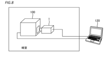
- FIG. 8 is a diagram illustrating an example of a correction value acquisition method. Here, a method for obtaining the gain G i and the gain G pi will be described.
- the imaging sensor 22 of the measurement device 1 is housed in a luminance box 100 with a specified illuminance, as illustrated in FIG. Then, the control computer 120 measures the sensitivity for each tap (for each storage unit CS) with respect to irradiation of the specified illuminance.
- the brightness box 100 irradiates the measuring device 1 (or the imaging sensor 22) with uniform light with a specified illuminance.
- T on 0; see formulas (6-1) to (6-4)
- the control computer 120 acquires the gain G i (gain correction value) and the gain G pi (parasitic correction value) for each tap (for each storage unit CS) of each pixel of the image sensor 22 . Then, the control computer 120 stores the gain G i (gain correction value) and the gain G pi (parasitic correction value) in the correction unit 35 of the control unit 30 of the measurement apparatus 1 in association with the storage unit CS of each pixel of the imaging sensor 22 . This enables the correcting section to correct the signal value Si according to the above-described second embodiment.
- the measuring device 1 includes an imaging sensor 22 (sensor), an image acquisition section 34 (signal acquisition section), and a correction section 35 .
- the imaging sensor 22 has a light-receiving element PD that generates charges according to the amount of exposure, and storage units CS1 to CS4 that store charges distributed according to the exposure period.
- the image acquisition unit 34 acquires signal values S 1 to S 4 corresponding to the charges in the storage units CS1 to CS4, respectively.
- the correction unit 35 specifies the minimum signal value S min indicating the smallest exposure amount from among the signal values S 1 to S 4 and corrects the signal values S 1 to S 4 based on the minimum signal value S min . This makes it possible to improve the frame rate (FPS) compared to the comparative example while suppressing the influence of background light.
- FPS frame rate
- the correction section 35 has the first correction value ⁇ i corresponding to the signal value S i when there is no reflected light, corresponding to each of the storage sections CS1 to CS4. Then, the correction unit 35 corrects the signal value S i corrected by the first correction value ⁇ i based on the minimum signal value S min corrected by the first correction value ⁇ i (see formulas (9-1) to (9-4)). As a result, the frame rate (FPS) can be improved while suppressing the influence of background light.
- the gain G pi corresponds to a correction value for correcting the parasitic sensitivity
- the correction unit 35 calculates the first correction value ⁇ i based on the gain G pi . This makes it possible to correct for the effects of parasitic sensitivities.
- the correction section 35 has a second correction value ⁇ i for correcting the gain variation of the signal value S i corresponding to each of the accumulation sections CS1 to CS4. Then, the correction unit 35 corrects the signal value S i corrected based on the minimum signal value S min based on the second correction value ⁇ i (see formulas (10-1) to (10-4)). Thereby, it is possible to suppress variation in gain for each tap.
- the correction unit 35 calculates the second correction value ⁇ i based on the first correction value ⁇ i and the gain G i . This makes it possible to suppress the influence of variations in gain and variations in parasitic sensitivity.
- the image acquisition unit 34 acquires signal values S 1 to S 4 corresponding to the charges accumulated in the storage units CS1 to CS4 during a plurality of exposure periods, and the correction unit 35 calculates the first correction value ⁇ i based on the number of exposure periods n i of the storage unit CSi (see formula (12)).
- the appropriate first correction value ⁇ i can be calculated for each storage unit CS, so the signal value corresponding to each storage unit CS can be appropriately corrected.
- the measuring device 1 further includes a distance calculator 38 that calculates the distance to the object based on the signal value corrected by the corrector 35 . Thereby, the precision of distance can be improved. Also, a distance image can be acquired by calculating the distance for each pixel.
- a sensor having a light-receiving element that generates a charge corresponding to an exposure amount, and a plurality of accumulation units that accumulate the charges distributed according to an exposure period; a signal acquisition unit that acquires signal values corresponding to the charges of the plurality of storage units; and a correction unit that specifies a minimum signal value indicating that the exposure amount is the smallest from among the plurality of signal values, and corrects the signal value based on the minimum signal value.
- the correction unit Each storage unit has a first correction value corresponding to the signal value when there is no reflected light, The measuring apparatus according to (1), wherein the signal value corrected by the first correction value is corrected based on the minimum signal value corrected by the first correction value.
- the correction unit each storage unit has a parasitic correction value corresponding to the signal value when no exposure period is provided; The measuring device according to (2), wherein the first correction value is calculated based on the parasitic correction value.
- the correction unit a second correction value for correcting variations in the gain of the signal value corresponding to each of the accumulation units; The measuring device according to (2) or (3), wherein the signal value corrected based on the minimum signal value is corrected based on the second correction value.
- the correction unit The measuring device according to (4), wherein the second correction value is calculated based on the first correction value and a gain correction value corresponding to the gain.
- the signal acquisition unit acquires a signal value corresponding to the electric charge of the accumulation unit accumulated during the exposure period a plurality of times;
- the measuring apparatus according to any one of (2) to (5), wherein the correction unit calculates the first correction value based on the number of exposure periods.
- the measuring device according to any one of (1) to (6), further comprising a calculator that calculates the distance to the object based on the corrected signal value.
Landscapes
- Physics & Mathematics (AREA)
- Engineering & Computer Science (AREA)
- General Physics & Mathematics (AREA)
- Radar, Positioning & Navigation (AREA)
- Remote Sensing (AREA)
- Electromagnetism (AREA)
- Computer Networks & Wireless Communication (AREA)
- Optical Radar Systems And Details Thereof (AREA)
Abstract
Priority Applications (1)
| Application Number | Priority Date | Filing Date | Title |
|---|---|---|---|
| CN202280089407.9A CN118575098A (zh) | 2022-01-21 | 2022-11-24 | 测量装置 |
Applications Claiming Priority (2)
| Application Number | Priority Date | Filing Date | Title |
|---|---|---|---|
| JP2022-007779 | 2022-01-21 | ||
| JP2022007779 | 2022-01-21 |
Publications (1)
| Publication Number | Publication Date |
|---|---|
| WO2023139916A1 true WO2023139916A1 (fr) | 2023-07-27 |
Family
ID=87348012
Family Applications (1)
| Application Number | Title | Priority Date | Filing Date |
|---|---|---|---|
| PCT/JP2022/043297 WO2023139916A1 (fr) | 2022-01-21 | 2022-11-24 | Dispositif de mesure |
Country Status (2)
| Country | Link |
|---|---|
| CN (1) | CN118575098A (fr) |
| WO (1) | WO2023139916A1 (fr) |
Cited By (1)
| Publication number | Priority date | Publication date | Assignee | Title |
|---|---|---|---|---|
| CN117241299A (zh) * | 2023-11-10 | 2023-12-15 | 中国民用航空飞行学院 | 一种航空电子数据安全性分析保护方法 |
Citations (7)
| Publication number | Priority date | Publication date | Assignee | Title |
|---|---|---|---|---|
| JP2008249673A (ja) * | 2007-03-30 | 2008-10-16 | Fujifilm Corp | 測距装置、測距方法及び測距システム |
| JP2019191118A (ja) * | 2018-04-27 | 2019-10-31 | ソニーセミコンダクタソリューションズ株式会社 | 測距処理装置、測距モジュール、測距処理方法、およびプログラム |
| JP2020052001A (ja) * | 2018-09-28 | 2020-04-02 | パナソニックIpマネジメント株式会社 | 奥行取得装置、奥行取得方法およびプログラム |
| JP2021025833A (ja) | 2019-08-01 | 2021-02-22 | 株式会社ブルックマンテクノロジ | 距離画像撮像装置、及び距離画像撮像方法 |
| WO2021177045A1 (fr) * | 2020-03-04 | 2021-09-10 | ソニーグループ株式会社 | Dispositif de traitement de signal, procédé de traitement de signal et module de télémétrie |
| JP2022007779A (ja) | 2020-06-26 | 2022-01-13 | トヨタ自動車株式会社 | 車両用動力伝達装置の潤滑構造 |
| JP7014324B1 (ja) * | 2021-06-09 | 2022-02-15 | 凸版印刷株式会社 | 距離画像撮像装置及び距離画像撮像方法 |
-
2022
- 2022-11-24 CN CN202280089407.9A patent/CN118575098A/zh active Pending
- 2022-11-24 WO PCT/JP2022/043297 patent/WO2023139916A1/fr active Application Filing
Patent Citations (7)
| Publication number | Priority date | Publication date | Assignee | Title |
|---|---|---|---|---|
| JP2008249673A (ja) * | 2007-03-30 | 2008-10-16 | Fujifilm Corp | 測距装置、測距方法及び測距システム |
| JP2019191118A (ja) * | 2018-04-27 | 2019-10-31 | ソニーセミコンダクタソリューションズ株式会社 | 測距処理装置、測距モジュール、測距処理方法、およびプログラム |
| JP2020052001A (ja) * | 2018-09-28 | 2020-04-02 | パナソニックIpマネジメント株式会社 | 奥行取得装置、奥行取得方法およびプログラム |
| JP2021025833A (ja) | 2019-08-01 | 2021-02-22 | 株式会社ブルックマンテクノロジ | 距離画像撮像装置、及び距離画像撮像方法 |
| WO2021177045A1 (fr) * | 2020-03-04 | 2021-09-10 | ソニーグループ株式会社 | Dispositif de traitement de signal, procédé de traitement de signal et module de télémétrie |
| JP2022007779A (ja) | 2020-06-26 | 2022-01-13 | トヨタ自動車株式会社 | 車両用動力伝達装置の潤滑構造 |
| JP7014324B1 (ja) * | 2021-06-09 | 2022-02-15 | 凸版印刷株式会社 | 距離画像撮像装置及び距離画像撮像方法 |
Cited By (2)
| Publication number | Priority date | Publication date | Assignee | Title |
|---|---|---|---|---|
| CN117241299A (zh) * | 2023-11-10 | 2023-12-15 | 中国民用航空飞行学院 | 一种航空电子数据安全性分析保护方法 |
| CN117241299B (zh) * | 2023-11-10 | 2024-01-23 | 中国民用航空飞行学院 | 一种航空电子数据安全性分析保护方法 |
Also Published As
| Publication number | Publication date |
|---|---|
| CN118575098A (zh) | 2024-08-30 |
Similar Documents
| Publication | Publication Date | Title |
|---|---|---|
| JP6676866B2 (ja) | 測距撮像装置及び固体撮像素子 | |
| WO2017150246A1 (fr) | Dispositif d'imagerie et élément d'imagerie à semi-conducteurs utilisé dans celui-ci | |
| US20110304696A1 (en) | Time-of-flight imager | |
| JP7157529B2 (ja) | 撮像装置、撮像システム、および撮像装置の駆動方法 | |
| EP3334152B1 (fr) | Dispositif d'imagerie à semi-conducteurs | |
| US20080231832A1 (en) | Ranging apparatus and ranging method | |
| US7671915B2 (en) | Solid-state imaging apparatus | |
| JP2011064498A (ja) | 測距装置、測距方法、及びそのプログラム | |
| JP2007214932A (ja) | 固定パターン雑音除去装置、固体撮像装置、電子機器、及び固定パターン雑音除去プログラム | |
| WO2023139916A1 (fr) | Dispositif de mesure | |
| US7956915B2 (en) | Solid-state imaging apparatus | |
| JP2017208604A (ja) | 画像処理装置、画像処理方法、撮像装置、プログラム | |
| JP2015161906A (ja) | 撮像装置 | |
| JPWO2020027221A1 (ja) | 撮像装置、それに用いられる固体撮像素子及び撮像方法 | |
| JP2017225072A (ja) | 撮像装置、その制御方法、及びプログラム | |
| JP6393091B2 (ja) | 撮像装置及びその制御方法、プログラム、記憶媒体 | |
| CN113597567A (zh) | 距离图像的获得方法、以及距离检测装置 | |
| US9402069B2 (en) | Depth measurement apparatus, imaging apparatus, and method of controlling depth measurement apparatus | |
| WO2023120012A1 (fr) | Dispositif de mesure | |
| WO2023166988A1 (fr) | Dispositif de mesure | |
| WO2023135943A1 (fr) | Dispositif de mesure | |
| WO2023171345A1 (fr) | Circuit de conversion photoélectrique et dispositif de conversion photoélectrique | |
| JP5720213B2 (ja) | 撮像装置 | |
| JP6366341B2 (ja) | 撮像装置 | |
| JP2010210810A (ja) | 焦点検出装置 |
Legal Events
| Date | Code | Title | Description |
|---|---|---|---|
| 121 | Ep: the epo has been informed by wipo that ep was designated in this application |
Ref document number: 22922067 Country of ref document: EP Kind code of ref document: A1 |
|
| ENP | Entry into the national phase |
Ref document number: 2023575091 Country of ref document: JP Kind code of ref document: A |
|
| WWE | Wipo information: entry into national phase |
Ref document number: 2022922067 Country of ref document: EP |
|
| ENP | Entry into the national phase |
Ref document number: 2022922067 Country of ref document: EP Effective date: 20240821 |