WO2023136306A1 - 撮像装置、カメラモジュール、及び撮像装置の制御方法 - Google Patents
撮像装置、カメラモジュール、及び撮像装置の制御方法 Download PDFInfo
- Publication number
- WO2023136306A1 WO2023136306A1 PCT/JP2023/000662 JP2023000662W WO2023136306A1 WO 2023136306 A1 WO2023136306 A1 WO 2023136306A1 JP 2023000662 W JP2023000662 W JP 2023000662W WO 2023136306 A1 WO2023136306 A1 WO 2023136306A1
- Authority
- WO
- WIPO (PCT)
- Prior art keywords
- memory alloy
- shape memory
- wire
- conductive path
- alloy wire
- Prior art date
- Legal status (The legal status is an assumption and is not a legal conclusion. Google has not performed a legal analysis and makes no representation as to the accuracy of the status listed.)
- Ceased
Links
Images













Classifications
-
- G—PHYSICS
- G03—PHOTOGRAPHY; CINEMATOGRAPHY; ANALOGOUS TECHNIQUES USING WAVES OTHER THAN OPTICAL WAVES; ELECTROGRAPHY; HOLOGRAPHY
- G03B—APPARATUS OR ARRANGEMENTS FOR TAKING PHOTOGRAPHS OR FOR PROJECTING OR VIEWING THEM; APPARATUS OR ARRANGEMENTS EMPLOYING ANALOGOUS TECHNIQUES USING WAVES OTHER THAN OPTICAL WAVES; ACCESSORIES THEREFOR
- G03B5/00—Adjustment of optical system relative to image or object surface other than for focusing
-
- F—MECHANICAL ENGINEERING; LIGHTING; HEATING; WEAPONS; BLASTING
- F03—MACHINES OR ENGINES FOR LIQUIDS; WIND, SPRING, OR WEIGHT MOTORS; PRODUCING MECHANICAL POWER OR A REACTIVE PROPULSIVE THRUST, NOT OTHERWISE PROVIDED FOR
- F03G—SPRING, WEIGHT, INERTIA OR LIKE MOTORS; MECHANICAL-POWER PRODUCING DEVICES OR MECHANISMS, NOT OTHERWISE PROVIDED FOR OR USING ENERGY SOURCES NOT OTHERWISE PROVIDED FOR
- F03G7/00—Mechanical-power-producing mechanisms, not otherwise provided for or using energy sources not otherwise provided for
- F03G7/06—Mechanical-power-producing mechanisms, not otherwise provided for or using energy sources not otherwise provided for using expansion or contraction of bodies due to heating, cooling, moistening, drying or the like
- F03G7/061—Mechanical-power-producing mechanisms, not otherwise provided for or using energy sources not otherwise provided for using expansion or contraction of bodies due to heating, cooling, moistening, drying or the like characterised by the actuating element
- F03G7/0614—Mechanical-power-producing mechanisms, not otherwise provided for or using energy sources not otherwise provided for using expansion or contraction of bodies due to heating, cooling, moistening, drying or the like characterised by the actuating element using shape memory elements
- F03G7/06143—Wires
-
- G—PHYSICS
- G02—OPTICS
- G02B—OPTICAL ELEMENTS, SYSTEMS OR APPARATUS
- G02B27/00—Optical systems or apparatus not provided for by any of the groups G02B1/00 - G02B26/00, G02B30/00
- G02B27/64—Imaging systems using optical elements for stabilisation of the lateral and angular position of the image
- G02B27/646—Imaging systems using optical elements for stabilisation of the lateral and angular position of the image compensating for small deviations, e.g. due to vibration or shake
-
- G—PHYSICS
- G02—OPTICS
- G02B—OPTICAL ELEMENTS, SYSTEMS OR APPARATUS
- G02B7/00—Mountings, adjusting means, or light-tight connections, for optical elements
- G02B7/02—Mountings, adjusting means, or light-tight connections, for optical elements for lenses
- G02B7/04—Mountings, adjusting means, or light-tight connections, for optical elements for lenses with mechanism for focusing or varying magnification
-
- G—PHYSICS
- G02—OPTICS
- G02B—OPTICAL ELEMENTS, SYSTEMS OR APPARATUS
- G02B7/00—Mountings, adjusting means, or light-tight connections, for optical elements
- G02B7/02—Mountings, adjusting means, or light-tight connections, for optical elements for lenses
- G02B7/04—Mountings, adjusting means, or light-tight connections, for optical elements for lenses with mechanism for focusing or varying magnification
- G02B7/08—Mountings, adjusting means, or light-tight connections, for optical elements for lenses with mechanism for focusing or varying magnification adapted to co-operate with a remote control mechanism
-
- G—PHYSICS
- G03—PHOTOGRAPHY; CINEMATOGRAPHY; ANALOGOUS TECHNIQUES USING WAVES OTHER THAN OPTICAL WAVES; ELECTROGRAPHY; HOLOGRAPHY
- G03B—APPARATUS OR ARRANGEMENTS FOR TAKING PHOTOGRAPHS OR FOR PROJECTING OR VIEWING THEM; APPARATUS OR ARRANGEMENTS EMPLOYING ANALOGOUS TECHNIQUES USING WAVES OTHER THAN OPTICAL WAVES; ACCESSORIES THEREFOR
- G03B13/00—Viewfinders; Focusing aids for cameras; Means for focusing for cameras; Autofocus systems for cameras
- G03B13/32—Means for focusing
- G03B13/34—Power focusing
- G03B13/36—Autofocus systems
-
- G—PHYSICS
- G03—PHOTOGRAPHY; CINEMATOGRAPHY; ANALOGOUS TECHNIQUES USING WAVES OTHER THAN OPTICAL WAVES; ELECTROGRAPHY; HOLOGRAPHY
- G03B—APPARATUS OR ARRANGEMENTS FOR TAKING PHOTOGRAPHS OR FOR PROJECTING OR VIEWING THEM; APPARATUS OR ARRANGEMENTS EMPLOYING ANALOGOUS TECHNIQUES USING WAVES OTHER THAN OPTICAL WAVES; ACCESSORIES THEREFOR
- G03B3/00—Focusing arrangements of general interest for cameras, projectors or printers
- G03B3/10—Power-operated focusing
-
- G—PHYSICS
- G03—PHOTOGRAPHY; CINEMATOGRAPHY; ANALOGOUS TECHNIQUES USING WAVES OTHER THAN OPTICAL WAVES; ELECTROGRAPHY; HOLOGRAPHY
- G03B—APPARATUS OR ARRANGEMENTS FOR TAKING PHOTOGRAPHS OR FOR PROJECTING OR VIEWING THEM; APPARATUS OR ARRANGEMENTS EMPLOYING ANALOGOUS TECHNIQUES USING WAVES OTHER THAN OPTICAL WAVES; ACCESSORIES THEREFOR
- G03B30/00—Camera modules comprising integrated lens units and imaging units, specially adapted for being embedded in other devices, e.g. mobile phones or vehicles
-
- H—ELECTRICITY
- H04—ELECTRIC COMMUNICATION TECHNIQUE
- H04N—PICTORIAL COMMUNICATION, e.g. TELEVISION
- H04N23/00—Cameras or camera modules comprising electronic image sensors; Control thereof
- H04N23/50—Constructional details
-
- H—ELECTRICITY
- H04—ELECTRIC COMMUNICATION TECHNIQUE
- H04N—PICTORIAL COMMUNICATION, e.g. TELEVISION
- H04N23/00—Cameras or camera modules comprising electronic image sensors; Control thereof
- H04N23/57—Mechanical or electrical details of cameras or camera modules specially adapted for being embedded in other devices
-
- G—PHYSICS
- G03—PHOTOGRAPHY; CINEMATOGRAPHY; ANALOGOUS TECHNIQUES USING WAVES OTHER THAN OPTICAL WAVES; ELECTROGRAPHY; HOLOGRAPHY
- G03B—APPARATUS OR ARRANGEMENTS FOR TAKING PHOTOGRAPHS OR FOR PROJECTING OR VIEWING THEM; APPARATUS OR ARRANGEMENTS EMPLOYING ANALOGOUS TECHNIQUES USING WAVES OTHER THAN OPTICAL WAVES; ACCESSORIES THEREFOR
- G03B2205/00—Adjustment of optical system relative to image or object surface other than for focusing
- G03B2205/0007—Movement of one or more optical elements for control of motion blur
-
- G—PHYSICS
- G03—PHOTOGRAPHY; CINEMATOGRAPHY; ANALOGOUS TECHNIQUES USING WAVES OTHER THAN OPTICAL WAVES; ELECTROGRAPHY; HOLOGRAPHY
- G03B—APPARATUS OR ARRANGEMENTS FOR TAKING PHOTOGRAPHS OR FOR PROJECTING OR VIEWING THEM; APPARATUS OR ARRANGEMENTS EMPLOYING ANALOGOUS TECHNIQUES USING WAVES OTHER THAN OPTICAL WAVES; ACCESSORIES THEREFOR
- G03B2205/00—Adjustment of optical system relative to image or object surface other than for focusing
- G03B2205/0053—Driving means for the movement of one or more optical element
- G03B2205/0076—Driving means for the movement of one or more optical element using shape memory alloys
Definitions
- the present disclosure relates to an imaging device, a camera module, and a control method for the imaging device.
- an imaging device using eight shape memory alloy wires is known (see Patent Document 1).
- the control circuit uses the PWM signal to individually supply electric current to each of the eight shape memory alloy wires to cause them to heat and contract, thereby moving the lens holder connected to the eight shape memory alloy wires. are moving.
- the control circuit includes a conductive path for passing a predetermined current through one of the eight shape memory alloy wires that is to be heated, and one of the eight shape memory alloy wires that is not to be heated.
- the driving circuit is controlled so that parallel-connected conductive paths are simultaneously formed in the remaining seven lines for passing a predetermined current divided by seven. With this configuration, the control circuit can appropriately heat and shrink a specific shape memory alloy wire.
- the imaging apparatus described above there is a risk that a relatively large magnetic field (induced magnetic field) will be formed around the conducting path for passing current through one of the objects to be heated. Then, the relatively large magnetic field becomes a noise source for the imaging device, and may adversely affect the image quality of the imaging device.
- a relatively large magnetic field induced magnetic field
- an imaging device that can reduce the magnitude of the magnetic field formed around the conductive path for supplying current to the shape memory alloy wire.
- An image pickup apparatus includes a fixed member including a fixed base, and a lens holder capable of holding a lens body so as to face an image sensor, and is movable with respect to the fixed member.
- a movable-side member including a fixed base, and a lens holder capable of holding a lens body so as to face an image sensor, and is movable with respect to the fixed member.
- a movable-side member including a first shape memory alloy wire having one end fixed to the fixed-side member and the other end fixed to the movable-side member; a second shape memory alloy wire fixed to a movable member; a first conductive path provided on the fixed base and electrically connected to one end of the first shape memory alloy wire; a second conductive path provided and electrically connected to one end of the second shape memory alloy wire; and electrically connected to the other ends of the first shape memory alloy wire and the second shape memory alloy wire.
- a driving device capable of supplying a current to each of the alloy wires to drive each of the first shape memory alloy wire and the second shape memory alloy wire, wherein a first point and a second point on the first conductive path;
- the portion connecting the points and the portion connecting the first point and the second point on the second conducting path are installed so as to be parallel to each other on the fixed base.
- a point is juxtaposed with a first point on the second conducting path
- a second point on the first conducting path is juxtaposed with a second point on the second conducting path
- the driving device comprises: and electrically connecting the first conductive path, the first shape memory alloy wire, the common conductive path, the second shape memory alloy wire, and the second conductive path in series to form the first shape memory alloy wire. and supplying current to the second shape memory alloy wire such that current flows from the first point to the second point on the first conductive path and current flows from the second point to the first point on the second conductive path.
- the first conductive path, the first shape memory alloy wire, and the common conductive path are electrically connected in series to supply current to the first shape memory alloy wire to supply the first mode.
- a second mode for allowing a current to flow through one conductive path
- a third mode in which a current is supplied to the second conductive path so that the current flows in the second conductive path, and the first mode, the second mode, and the third mode. is configured to be executed in combination with at least one of
- the imaging device described above can reduce the magnitude of the magnetic field formed around the conductive path for supplying current to the shape memory alloy wire.
- FIG. 1 is a perspective view of an imaging device;
- FIG. 1 is an exploded perspective view of an imaging device;
- FIG. 4 is a perspective view of a lens holder to which a movable-side metal member and leaf springs are attached;
- FIG. 4 is a perspective view of a base member to which a stationary-side metal member is attached;
- FIG. 4 is a side view of a metal member to which a shape memory alloy wire is attached;
- FIG. 4 is a top view of a metal member to which a shape memory alloy wire is attached; It is a perspective view of a base member.
- FIG. 4 is a perspective view of a lens holder to which a movable-side metal member and leaf springs are attached;
- FIG. 4 is a perspective view of a base member to which a stationary-side metal member is attached;
- FIG. 4 is a side view of a metal member to which a shape memory alloy wire is attached;
- FIG. 4 is a top view of a
- FIG. 4 is a diagram showing the positional relationship among leaf springs, shape memory alloy wires, metal members, and conductive members; It is a figure which shows the positional relationship of a leaf
- FIG. 4 is a diagram showing an example of a path of current flowing through a shape memory alloy wire;
- FIG. 10 is a diagram showing another example of a path of current flowing through a shape memory alloy wire;
- FIG. 10 is a diagram showing yet another example of a path of current flowing through a shape memory alloy wire;
- FIG. 10 is a diagram showing yet another example of a path of current flowing through a shape memory alloy wire;
- FIG. 10 is a diagram showing yet another example of a path of current flowing through a shape memory alloy wire;
- FIG. 10 is a diagram showing yet another example of a path of current flowing through a shape memory alloy wire;
- FIG. 10 is a diagram showing yet another example of a path of current flowing through a shape memory alloy wire;
- FIG. 10
- FIG. 10 is a diagram showing yet another example of a path of current flowing through a shape memory alloy wire; It is a figure which shows an example of the connection structure which connects a fixed side metal member and an electrically-conductive member. It is a figure which shows an example of the connection structure which connects a fixed side metal member and an electrically-conductive member. It is a figure which shows the structural example of a drive device and a control device. It is a figure which shows an example of the path
- FIG. 5 is a diagram showing another example of current paths in the drive device;
- FIG. 10 is a diagram showing still another example of a current path in the driving device; FIG.
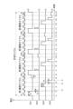
- FIG. 10 is a diagram showing still another example of a current path in the driving device; It is an example of a timing chart of a driving current and a measuring current flowing through a shape memory alloy wire. It is a perspective view of a first conductive member and a second conductive member. It is another example of the timing chart of the driving current and the measuring current flowing through the shape memory alloy wire. It is a figure showing another example of composition of a drive.
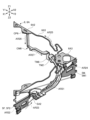
- FIG. 1 is a perspective view of an imaging device 101.
- FIG. 2 is an exploded perspective view of the imaging device 101.
- FIG. 1 is a perspective view of an imaging device 101.
- FIG. 2 is an exploded perspective view of the imaging device 101.
- X1 represents one direction of the X-axis that constitutes the three-dimensional orthogonal coordinate system
- X2 represents the other direction of the X-axis
- Y1 represents one direction of the Y-axis forming the three-dimensional orthogonal coordinate system
- Y2 represents the other direction of the Y-axis
- Z1 represents one direction of the Z-axis forming the three-dimensional orthogonal coordinate system
- Z2 represents the other direction of the Z-axis.
- the X1 side of the imaging device 101 corresponds to the front side (front side) of the imaging device 101
- the X2 side of the imaging device 101 corresponds to the rear side (back side) of the imaging device 101.
- the Y1 side of the imaging device 101 corresponds to the left side of the imaging device 101
- the Y2 side of the imaging device 101 corresponds to the right side of the imaging device 101
- the Z1 side of the imaging device 101 corresponds to the upper side of the imaging device 101 (object side)
- the Z2 side of the imaging device 101 corresponds to the lower side of the imaging device 101 (imaging element side). The same applies to other drawings.
- the imaging device 101 includes a cover member 4 that is part of the fixed side member FB.
- the cover member 4 is configured to function as a housing that covers other members.
- the cover member 4 is made of non-magnetic metal.
- the cover member 4 may be made of a magnetic metal.
- the cover member 4 defines a storage portion 4S, as shown in FIG.
- the cover member 4 has a rectangular tubular outer peripheral wall portion 4A and a rectangular annular flat plate-like top plate portion 4B provided so as to be continuous with the upper end (the end on the Z1 side) of the outer peripheral wall portion 4A.
- a circular opening 4K is formed in the center of the top plate portion 4B.
- the outer peripheral wall portion 4A includes a first side plate portion 4A1 to a fourth side plate portion 4A4.
- the first side plate portion 4A1 and the third side plate portion 4A3 face each other, and the second side plate portion 4A2 and the fourth side plate portion 4A4 face each other.
- the first side plate portion 4A1 and the third side plate portion 4A3 extend perpendicularly to the second side plate portion 4A2 and the fourth side plate portion 4A4.
- the lens holder 2 Inside the cover member 4, as shown in FIG. 2, the lens holder 2, the metal member 5, the plate spring 6, the base member 18, the shape memory alloy wire SA, etc. are accommodated.
- the movable side member MB includes a lens holder 2 capable of holding a lens body (not shown) and a leaf spring 6 supporting the lens holder 2 so as to be movable along the optical axis OA.
- the lens body is, for example, a cylindrical lens barrel having at least one lens, and its central axis is arranged along the optical axis OA.
- the lens holder 2 is formed by injection molding synthetic resin such as liquid crystal polymer (LCP). Specifically, as shown in FIG. 2, the lens holder 2 has a cylindrical portion 2P formed to extend along the optical axis OA, and a cylindrical portion 2P formed to protrude radially outward from the cylindrical portion 2P. and a movable side pedestal portion 2D and a projecting portion 2S. In this embodiment, the lens body is configured to be fixed to the inner peripheral surface of the cylindrical portion 2P with an adhesive.
- LCP liquid crystal polymer
- the movable-side pedestal portion 2D includes a first movable-side pedestal portion 2D1 and a second movable-side pedestal portion 2D2.
- the first movable-side pedestal portion 2D1 and the second movable-side pedestal portion 2D2 are arranged so as to protrude in mutually opposite directions with the optical axis OA interposed therebetween.
- the projecting portion 2S includes a first projecting portion 2S1 and a second projecting portion 2S2.
- the first projecting portion 2S1 and the second projecting portion 2S2 are arranged to project in opposite directions with the optical axis OA interposed therebetween.
- the movable-side pedestal portion 2D and the projecting portion 2S are arranged so as to correspond to the four corners of the lens holder 2, which has a substantially rectangular outer shape when viewed from above, and are arranged alternately. are placed. A part of the leaf spring 6 is placed on each of the two movable-side pedestals 2D.
- the shape memory alloy wire SA is an example of a shape memory actuator.
- the shape memory alloy wires SA include first wires SA1 to eighth wires SA8.
- the shape memory alloy wire SA increases in temperature when current flows, and contracts according to the increase in temperature.
- the imaging device 101 can move the lens holder 2 up and down along the optical axis OA using contraction of the shape memory alloy wire SA.
- the lens holder 2 moves, and another one or more of the shape memory alloy wires SA move due to the movement. configured to be stretched.
- the leaf spring 6 is configured to be electrically connected to the shape memory alloy wire SA through the metal member 5 .
- the leaf spring 6 is made of a metal plate mainly made of, for example, a copper alloy, a titanium-copper alloy (titanium-copper), or a copper-nickel alloy (nickel-tin-copper).
- the leaf springs 6 include a first leaf spring 6A and a second leaf spring 6B.
- the base member 18 (fixed base) is formed by injection molding using synthetic resin such as liquid crystal polymer (LCP).
- LCP liquid crystal polymer
- the base member 18 has a substantially rectangular outline when viewed from above, and has an opening 18K in the center.
- the base member 18 has four side portions 18E (first side portion 18E1 to fourth side portion 18E4) arranged to surround the opening 18K.
- the leaf spring 6 is configured to connect the movable side pedestal portion 2D formed on the lens holder 2 and the fixed side pedestal portion 18D formed on the base member 18 .
- the fixed side pedestal portion 18D includes a first fixed side pedestal portion 18D1 and a second fixed side pedestal portion 18D2.
- the first plate spring 6A includes a first movable side seat portion 2D1 formed on the lens holder 2, and a first fixed side seat portion 18D1 and a second fixed side seat portion 18D1 formed on the base member 18. 18D2.
- the second plate spring 6B is formed by a second movable side pedestal portion 2D2 formed on the lens holder 2, and a first fixed side pedestal portion 18D1 and a second fixed side pedestal portion 18D2 formed on the base member 18, respectively. It is configured to connect with
- the metal member 5 is configured so that the end of the shape memory alloy wire SA is fixed.
- the metal member 5 includes a fixed side metal member 5F and a movable side metal member 5M.
- the fixed-side metal member 5 ⁇ /b>F constitutes a part of the fixed-side member FB and is configured to be fixed to the fixed-side pedestal portion 18 ⁇ /b>D of the base member 18 .
- the movable-side metal member 5 ⁇ /b>M constitutes a part of the movable-side member MB and is configured to be fixed to the movable-side pedestal portion 2 ⁇ /b>D of the lens holder 2 .
- the fixed-side metal member 5F is also called a fixed-side terminal plate, and includes a first fixed-side terminal plate 5F1 to an eighth fixed-side terminal plate 5F8.
- the movable-side metal member 5M is also called a movable-side terminal plate, and includes a first movable-side terminal plate 5M1 to a fourth movable-side terminal plate 5M4.
- FIG. 3A is a perspective view of the lens holder 2 to which the movable-side metal member 5M (movable-side terminal plate) and leaf spring 6 are attached.
- FIG. 3B is a perspective view of the base member 18 to which the fixed-side metal member 5F (fixed-side terminal plate) is attached.
- the movable side metal member 5M and the plate spring 6 are marked with a dot pattern
- the fixed side metal member 5F is marked with a dot pattern.
- the first movable terminal plate 5M1 is fixed to the Y2 side wall (right mounting surface) of the first movable pedestal 2D1. Specifically, a rectangular projection 2V protruding outward (Y2 side) formed in the first movable side pedestal 2D1 and a rectangular hole AH (see FIG. 4A) formed in the first movable side terminal plate 5M1.
- the first movable side terminal plate 5M1 is fixed to the first movable side pedestal portion 2D1 with an adhesive in the engaged state.
- the adhesive is, for example, a photocurable adhesive.
- the photocurable adhesive is, for example, an ultraviolet curable adhesive or a visible light curable adhesive.
- the second movable-side terminal plate 5M2 is fixed to the side wall (rear mounting surface) on the X2 side of the first movable-side pedestal portion 2D1
- the third movable-side terminal plate 5M3 is fixed to the second movable-side pedestal portion 2D2.
- the fourth movable terminal plate 5M4 is fixed to the Y1 side wall (left mounting surface) of the second movable pedestal 2D2.
- the first stationary terminal plate 5F1 and the second stationary terminal plate 5F2 are located on the Y2 side of the first stationary pedestal 18D1 arranged along the second side 18E2 of the base member 18. It is fixed to the side wall (right mounting surface). Specifically, the first stationary terminal plate 5F1 and the second stationary terminal plate 5F2 are fixed to the first stationary pedestal portion 18D1 with an adhesive. More specifically, the second fixed-side terminal plate 5F2 is formed on the second fixed-side terminal plate 5F2 and the rectangular protrusion 18V that protrudes outward (Y2 side) formed on the first fixed-side pedestal portion 18D1. It is fixed to the first fixed-side pedestal portion 18D1 with an adhesive while engaging with the through hole RH (see FIG.
- the adhesive is, for example, a photocurable adhesive.
- the photocurable adhesive is, for example, an ultraviolet curable adhesive or a visible light curable adhesive.
- the third stationary terminal plate 5F3 and the fourth stationary terminal plate 5F4 (not visible in FIG. 3B) are arranged along the third side 18E3 of the base member 18 at X2 of the second stationary pedestal 18D2. side wall (rear mounting surface).
- the fifth stationary terminal plate 5F5 and the sixth stationary terminal plate 5F6 are arranged along the first side 18E1 of the base member 18 on the X1 side wall (front mounting surface) of the first stationary pedestal 18D1.
- the seventh stationary terminal plate 5F7 and the eighth stationary terminal plate 5F8 (not visible in FIG. 3B) are arranged along the fourth side 18E4 of the base member 18 on the Y1 side of the second stationary pedestal 18D2. is fixed to the side wall (left mounting surface) of the
- the shape memory alloy wire SA extends along the inner surface of the outer peripheral wall portion 4A of the cover member 4, and is configured to movably support the movable side member MB with respect to the fixed side member FB.
- the shape memory alloy wires SA include the first wire SA1 to the eighth wire SA8, and enable the lens holder 2 as the movable side member MB to move with respect to the base member 18 as the fixed side member FB. configured to support.
- each of the first wire SA1 to the eighth wire SA8 has one end fixed to the stationary metal member 5F by crimping or welding, and the other end thereof is crimped or welded to the movable metal member. It is attached to 5M.
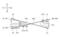
- FIG. 4A shows a first wire SA1 attached to each of the first movable terminal plate 5M1 and first fixed terminal plate 5F1, and a first wire SA1 attached to each of the first movable terminal plate 5M1 and second fixed terminal plate 5F2. It is a figure when seeing attached 2nd wire SA2 from the Y2 side.
- FIG. 4B shows a first wire SA1 attached to each of the first movable-side terminal plate 5M1 and the first fixed-side terminal plate 5F1, and a first wire SA1 attached to each of the first movable-side terminal plate 5M1 and the second fixed-side terminal plate 5F2.
- FIGS. 4A and 4B corresponds to the positional relationship when the imaging device 101 is assembled. 4A and 4B, illustration of other members is omitted for clarity. Also, the following description with reference to FIGS. 4A and 4B relates to the combination of the first wire SA1 and the second wire SA2, the combination of the third wire SA3 and the fourth wire SA4, the fifth wire SA5 and the sixth wire SA6. and the combination of the seventh wire SA7 and the eighth wire SA8.
- one end of the first wire SA1 is fixed to the first movable terminal plate 5M1 at the lower holding portion J3 of the first movable terminal plate 5M1, and the other end of the first wire SA1 is connected to the first movable terminal plate 5M1. It is fixed to the first fixed terminal plate 5F1 at the holding portion J2 of the first fixed terminal plate 5F1.
- one end of the second wire SA2 is fixed to the first movable terminal plate 5M1 at the upper holding portion J1 of the first movable terminal plate 5M1, and the other end of the second wire SA2 is fixed to the second fixed side. It is fixed to the second stationary terminal plate 5F2 at the holding portion J4 of the terminal plate 5F2.
- the holding portion J1 is formed by bending a portion of the first movable terminal plate 5M1. Specifically, a portion of the first movable terminal plate 5M1 forms a holding portion J1 by being bent while sandwiching one end of the second wire SA2. One end of the second wire SA2 is fixed to the holding portion J1 by welding. The same applies to the holding portions J2 to J4.
- the first wire SA1 and the second wire SA2 are arranged so as to be twisted relative to each other, as shown in FIGS. 4A and 4B. In other words, the first wire SA1 and the second wire SA2 are arranged so as not to contact each other (become non-contact).
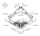
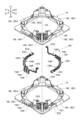
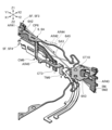
- FIG. 5 is a perspective view of the base member 18.
- FIG. Specifically, the upper view of FIG. 5 is a perspective view of the base member 18 with the conductive member CM removed, and the central view of FIG. 5 is a perspective view of the base member 18 in which the conductive member CM is embedded.
- the conductive member CM is given a dot pattern for clarity.
- the base member 18 is configured to function as a wire support member that supports one end of each of the first wire SA1 to the eighth wire SA8.
- the movable member MB is supported by the first wire SA1 to the eighth wire SA8 so as to be movable in the Z-axis direction parallel to the optical axis OA.
- a fixed-side pedestal portion 18D is formed on the upper surface of the base member 18, which is the object-side surface (Z1-side surface).
- the fixed-side pedestal portion 18D includes a first fixed-side pedestal portion 18D1 and a second fixed-side pedestal portion 18D2.
- the first fixed-side pedestal portion 18D1 and the second fixed-side pedestal portion 18D2 are arranged to face each other with the optical axis OA interposed therebetween.
- a conductive member CM formed of a metal plate containing a material such as copper, iron, or an alloy containing them as main components is embedded by insert molding.
- the conductive member CM is exposed from the front surface (X1 side surface) and the rear surface (X2 side surface) of the base member 18, and extends downward (Z2 direction) from the first terminal portion TM1 to the sixth terminal portion.
- TM6 and a fifth joint surface portion CP5 and a sixth joint surface portion CP6 exposed on the upper surface (the surface on the Z1 side) of the base member .
- the conductive member CM includes a first conductive member CM1 to a sixth conductive member CM6.
- the first conductive member CM1 includes a first terminal portion TM1 and a first connection portion ED1.
- the second conductive member CM2 includes a second terminal portion TM2 and a second connection portion ED2.
- the third conductive member CM3 includes a third terminal portion TM3 and a third connection portion ED3.
- the fourth conductive member CM4 includes a fourth terminal portion TM4 and a fourth connection portion ED4.
- the fifth conductive member CM5 includes a fifth terminal portion TM5 and a fifth joint surface portion CP5.
- the sixth conductive member CM6 includes a sixth terminal portion TM6 and a sixth joint surface portion CP6.
- the first terminal portion TM1, the second terminal portion TM2, and the sixth terminal portion TM6 are arranged along the third side portion 18E3 of the base member 18.
- the third terminal portion TM3 to the fifth terminal portion TM5 are arranged along the first side portion 18E1 of the base member .
- the first connection portion ED1 of the first conductive member CM1 is arranged along the second side portion 18E2 of the base member 18, and the first terminal portion TM1 of the first conductive member CM1 is arranged along the second side portion 18E2 of the base member 18. It is arranged along the third side portion 18E3 instead of the portion 18E2.
- the second connection portion ED2 of the second conductive member CM2 is arranged along the second side portion 18E2 of the base member 18, and the second terminal portion TM2 of the second conductive member CM2 is arranged along the second side portion 18E2 of the base member 18. It is arranged along the third side portion 18E3 instead of the side portion 18E2.
- the third connecting portion ED3 of the third conductive member CM3 is arranged along the fourth side 18E4 of the base member 18, and the third terminal portion TM3 of the third conductive member CM3 is arranged along the fourth side 18E4 of the base member 18. It is arranged along the first side portion 18E1 instead of the portion 18E4.
- the fourth connection portion ED4 of the fourth conductive member CM4 is arranged along the fourth side portion 18E4 of the base member 18, and the fourth terminal portion TM4 of the fourth conductive member CM4 is arranged along the fourth side portion 18E4 of the base member 18. It is arranged along the first side portion 18E1 instead of the side portion 18E4.
- the first terminal portion TM1 to the sixth terminal portion TM6 are arranged along the first side portion 18E1 or the third side portion 18E3 of the base member 18, and are arranged along the second side portion 18E2 and the fourth side portion 18E2 of the base member 18. It is not arranged along side 18E4. This is for facilitating mounting of the imaging device. Specifically, this is so that a flexible printed circuit board or the like connected to the imaging device can pass under at least one of the second side portion 18E2 and the fourth side portion 18E4 of the base member .
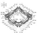
- FIG. 6 is a diagram showing the positional relationship among the leaf spring 6, shape memory alloy wire SA, metal member 5, and conductive member CM.
- FIG. 6A is a perspective view of the metal member 5, leaf spring 6, shape memory alloy wire SA, and conductive member CM
- FIG. 6B is a top view of the metal member 5 and leaf spring 6.
- FIG. 6B the shape memory alloy wire SA and the conductive member CM are omitted for clarity.
- FIGS. 6A and 6B the leaf spring 6 is marked with a dot pattern for clarity.
- the leaf spring 6 includes a first leaf spring 6A and a second leaf spring 6B, as shown in FIG. 6B.
- the first plate spring 6A includes a first portion 6A1 fixed to a first fixed side pedestal portion 18D1 (see FIG. 2) of the base member 18 and a second fixed side pedestal portion 18D2 (see FIG. 2) of the base member 18. ), a third portion 6A3 fixed to the first movable pedestal portion 2D1 (see FIG. 2) of the lens holder 2, and a fourth portion connecting the first portion 6A1 and the third portion 6A3. It has a portion 6A4 and a fifth portion 6A5 connecting the second portion 6A2 and the third portion 6A3.
- the first portion 6A1 is formed with a first through hole 6AH1 and a second through hole 6AH2 through which the upwardly protruding round protrusion 18T (see FIG. 3B) formed on the first fixed side pedestal 18D1 is inserted. It is In this embodiment, fixing between the plate spring 6 and the projecting portion 18T is achieved by subjecting the projecting portion 18T to hot crimping or cold crimping. However, the fixing between the plate spring 6 and the projecting portion 18T may be realized by an adhesive.
- a third through hole 6AH3 through which a round projecting portion 18T (see FIG. 3B) projecting upward formed on the second fixed side pedestal portion 18D2 is inserted, and a sixth conductive member CM6.
- a fourth through hole 6AH4 used for bonding with the sixth bonding surface portion CP6 (see the lower drawing in FIG. 5) is formed.
- the joining between the leaf spring 6 and the conductive member CM is realized by welding such as laser welding.
- the connection between the leaf spring 6 and the conductive member CM may be realized by solder, a conductive adhesive, or the like.
- the third portion 6A3 is formed with a fifth through-hole 6AH5 and a sixth through-hole 6AH6 through which the upwardly protruding round protrusion 2T (see FIG. 3A) formed on the first movable side pedestal 2D1 is inserted. It is In this embodiment, the fixing of the leaf spring 6 and the projecting portion 2T is achieved by subjecting the projecting portion 2T to hot crimping or cold crimping. However, the fixing between the plate spring 6 and the projecting portion 2T may be realized by an adhesive.
- the second plate spring 6B includes a first portion 6B1 fixed to a first fixed side seat portion 18D1 (see FIG. 2) of the base member 18 and a second fixed side seat portion 18D2 (see FIG. 2) of the base member 18. ), a third portion 6B3 fixed to the second movable side pedestal portion 2D2 (see FIG. 2) of the lens holder 2, and a third portion connecting the first portion 6B1 and the third portion 6B3. It has a fourth portion 6B4 and a fifth portion 6B5 connecting the second portion 6B2 and the third portion 6B3.
- the first portion 6B1 includes a first through hole 6BH1 through which the upwardly protruding round protrusion 18T (see FIG. 3B) formed on the first fixed side pedestal portion 18D1 is inserted, and a fifth conductive member CM5.
- a second through hole 6BH2 used for bonding with the fifth bonding surface portion CP5 (see the lower drawing in FIG. 5) is formed.
- the second portion 6B2 is formed with a third through-hole 6BH3 and a fourth through-hole 6BH4 through which the upwardly protruding round projection 18T (see FIG. 3B) formed on the second fixed side pedestal portion 18D2 is inserted. It is
- the third portion 6B3 is formed with a fifth through-hole 6BH5 and a sixth through-hole 6BH6 through which the upwardly projecting round protrusion 2T (see FIG. 3A) formed on the second movable side pedestal 2D2 is inserted. It is
- the fourth portion 6A4 and fifth portion 6A5 of the first leaf spring 6A and the fourth portion 6B4 and fifth portion 6B5 of the second leaf spring 6B are elastically deformable arms having a plurality of bent portions. Therefore, the lens holder 2 is movable with respect to the base member 18 (fixed member FB) not only in a direction parallel to the optical axis OA, but also in a direction crossing the optical axis OA.
- the first leaf spring 6A and the second leaf spring 6B have substantially the same shape.
- the first leaf spring 6A and the second leaf spring 6B are configured to have two-fold rotational symmetry with respect to the optical axis OA. Therefore, this configuration can reduce the number of parts of the imaging device 101 .
- the first plate spring 6A and the second plate spring 6B can support the lens holder 2 in the air with good balance.
- the leaf spring 6 does not adversely affect the weight balance of the movable side member MB supported by the eight shape memory alloy wires SA (first wire SA1 to eighth wire SA8).
- the first connection portion ED1 of the first conductive member CM1 is joined to the first contact portion CT1 of the adjacent first stationary terminal plate 5F1 with a joining material SD.
- the joint material SD is, for example, solder or a conductive adhesive.
- the first connection portion ED1 and the first contact portion CT1 are joined adjacent to each other with their surfaces substantially parallel to each other.
- the second connection portion ED2 of the second conductive member CM2 is joined to the second contact portion CT2 of the adjacent second fixed-side terminal plate 5F2 by the joining material SD
- the third connection portion ED3 of the third conductive member CM3 is joined to the seventh contact portion CT7 of the adjacent seventh stationary terminal plate 5F7 by the joining material SD
- the fourth connection portion ED4 of the fourth conductive member CM4 is joined to the eighth contact portion CT7 of the adjacent eighth stationary terminal plate 5F8. It is joined to the contact portion CT8 by a joining material SD.
- the bonding material SD is represented by a dashed circle for clarity.
- the ninth contact portion CT9 of the first movable terminal plate 5M1 is vertically joined to the third portion 6A3 of the first leaf spring 6A with a joining material SD. That is, the ninth contact portion CT9 and the third portion 6A3 are joined so that their surfaces are substantially perpendicular to each other.
- the tenth contact portion CT10 of the second movable-side terminal plate 5M2 is vertically joined to the third portion 6A3 of the first leaf spring 6A by the joining material SD
- the eleventh contact portion of the third movable-side terminal plate 5M3 CT11 is vertically joined to the third portion 6B3 of the second leaf spring 6B by the joining material SD
- the twelfth contact portion CT12 of the fourth movable terminal plate 5M4 is joined to the third portion 6B3 of the second leaf spring 6B by the joining material SD. It is joined vertically to part 6B3.
- the first stationary terminal plate 5F1 is arranged apart from the first portion 6A1 of the first leaf spring 6A, and the first portion 6A1 of the first leaf spring 6A has not in contact.
- the third stationary terminal plate 5F3 is not in contact with the second portion 6A2 of the first leaf spring 6A
- the fifth stationary terminal plate 5F5 is in contact with the first portion 6B1 of the second leaf spring 6B. are not in contact with each other, and the seventh stationary terminal plate 5F7 is not in contact with the second portion 6B2 of the second leaf spring 6B.
- the fifth joint surface portion CP5 (see the central view of FIG. 5) of the fifth conductive member CM5 is welded by laser welding or the like at the second through hole 6BH2 formed in the first portion 6B1 of the second plate spring 6B. It is joined parallel to the first portion 6B1 of the second leaf spring 6B. That is, the fifth joint surface portion CP5 and the first portion 6B1 are jointed with their surfaces substantially parallel to each other.
- the sixth joint surface portion CP6 (see the center view of FIG. 5) of the sixth conductive member CM6 is welded by laser welding or the like at the fourth through hole 6AH4 formed in the second portion 6A2 of the first leaf spring 6A. It is joined parallel to the second portion 6A2 of the first leaf spring 6A by welding.
- FIGS. 7A to 7F are views of a portion of the configuration shown in FIG. 6A.
- the members through which the current flows are marked with a dot pattern for clarity.
- the first conductive member CM1 and the second conductive member CM2 are provided with a rough dot pattern, and the first movable side terminal plate 5M1, the first fixed side terminal plate 5F1, and the second fixed side A fine dot pattern is applied to the terminal plate 5F2.
- FIG. 7A the first conductive member CM1 and the second conductive member CM2 are provided with a rough dot pattern, and the first movable side terminal plate 5M1, the first fixed side terminal plate 5F1, and the second fixed side A fine dot pattern is applied to the terminal plate 5F2.
- the first conductive member CM1 and the sixth conductive member CM6 are given a coarse dot pattern
- the first plate spring 6A is given a fine dot pattern
- the first movable terminal plate 5M1 and the first A finer dot pattern is applied to the fixed-side terminal plate 5F1.
- the second conductive member CM2 and the sixth conductive member CM6 are given a rough dot pattern
- the first plate spring 6A is given a fine dot pattern
- the first movable terminal plate 5M1 and the second A finer dot pattern is applied to the fixed-side terminal plate 5F2.
- fine dot patterns are applied to the second movable terminal plate 5M2, the third fixed terminal plate 5F3, and the fourth fixed terminal plate 5F4.
- the sixth conductive member CM6 has a rough dot pattern
- the first leaf spring 6A has a fine dot pattern
- the second movable terminal plate 5M2 and the third stationary terminal plate 5F3 have has a finer dot pattern.
- the sixth conductive member CM6 has a rough dot pattern
- the first leaf spring 6A has a fine dot pattern
- the second movable terminal plate 5M2 and the fourth fixed terminal plate 5F4 have has a finer dot pattern.
- FIG. 7A shows the current path when the first terminal portion TM1 of the first conductive member CM1 is connected to a high potential and the second terminal portion TM2 of the second conductive member CM2 is connected to a low potential.
- FIG. 7B shows current paths when the first terminal portion TM1 of the first conductive member CM1 is connected to a high potential and the sixth terminal portion TM6 of the sixth conductive member CM6 is connected to a low potential.
- FIG. 7C shows current paths when the second terminal portion TM2 of the second conductive member CM2 is connected to a high potential and the sixth terminal portion TM6 of the sixth conductive member CM6 is connected to a low potential.
- the following description with reference to FIGS. 7A to 7C relates to the path of current flowing through the first wire SA1 or the second wire SA2, but applies similarly to the path of current flowing through the seventh wire SA7 or the eighth wire SA8. be.
- the current flows as indicated by the arrow AR1 in FIG. 7A. It flows from the first terminal portion TM1 to the first stationary terminal plate 5F1 through the first conductive member CM1. After that, the current flows through the first fixed terminal plate 5F1 as indicated by arrow AR2, the first wire SA1 as indicated by arrow AR3, and the first movable terminal plate 5M1 as indicated by arrow AR4. pass. After that, the current flows through the second wire SA2 as indicated by arrow AR5, through the second stationary terminal plate 5F2 as indicated by arrow AR6, and through the second conductive member CM2 as indicated by arrow AR7. It flows to the second terminal portion TM2.
- the current flows as indicated by the arrow AR11 in FIG. 7B. It flows from the first terminal portion TM1 to the first stationary terminal plate 5F1 through the first conductive member CM1. After that, the current flows through the first fixed terminal plate 5F1 as indicated by arrow AR12, through the first wire SA1 as indicated by arrow AR13, and further through the first movable terminal plate 5M1 as indicated by arrow AR14. pass.
- the current then flows through the third portion 6A3, fifth portion 6A5 and second portion 6A2 of the first leaf spring 6A as indicated by arrow AR15, and through the sixth conducting member as indicated by arrows AR16 and AR17. It flows through CM6 to the sixth terminal portion TM6.
- the current flows as indicated by the arrow AR21 in FIG. 7C. It flows from the second terminal portion TM2 to the second stationary terminal plate 5F2 through the second conductive member CM2. After that, the current flows through the second fixed terminal plate 5F2 as indicated by an arrow AR22, the second wire SA2 as indicated by an arrow AR23, and the first movable terminal plate 5M1 as indicated by an arrow AR24. pass.
- the current then flows through the third portion 6A3, fifth portion 6A5 and second portion 6A2 of the first leaf spring 6A as indicated by arrow AR25, and through the sixth conducting member as indicated by arrows AR26 and AR27. It flows through CM6 to the sixth terminal portion TM6.
- FIG. 7D shows the current flow when the third contact CT3 of the third fixed terminal plate 5F3 is connected to a high potential and the fourth contact CT4 of the fourth fixed terminal plate 5F4 is connected to a low potential. indicate the route.
- FIG. 7E shows current paths when the third contact portion CT3 of the third stationary terminal plate 5F3 is connected to a high potential and the sixth terminal portion TM6 of the sixth conductive member CM6 is connected to a low potential.
- FIG. 7F shows current paths when the fourth contact portion CT4 of the fourth stationary terminal plate 5F4 is connected to a high potential and the sixth terminal portion TM6 of the sixth conductive member CM6 is connected to a low potential.
- the following description with reference to FIGS. 7D to 7F relates to the path of current flowing through the third wire SA3 or the fourth wire SA4, but applies equally to the path of current flowing through the fifth wire SA5 or the sixth wire SA6. be.
- the current flows as indicated by the arrow AR31 in FIG. 7D. , flows from the third contact portion CT3 to the third wire SA3 through the third stationary terminal plate 5F3. After that, the current flows through the third wire SA3 as indicated by arrow AR32, through the second movable terminal plate 5M2 as indicated by arrow AR33, and further through the fourth wire SA4 as indicated by arrow AR34. After that, the current flows through the fourth stationary terminal plate 5F4 to the fourth contact portion CT4 as indicated by an arrow AR35.
- the current is indicated by an arrow AR41 in FIG. 7E. , from the third contact portion CT3 to the third wire SA3 through the third stationary terminal plate 5F3. After that, the current flows through the third wire SA3 as indicated by an arrow AR42, through the second movable terminal plate 5M2 as indicated by an arrow AR43, and further through the third wire SA3 of the first leaf spring 6A as indicated by an arrow AR44. It passes through part 6A3, fifth part 6A5 and second part 6A2. Thereafter, current flows from the sixth joint surface portion CP6 to the sixth terminal portion TM6 through the sixth conductive member CM6 as indicated by an arrow AR45.
- the current is indicated by the arrow AR51 in FIG. 7F. , from the fourth contact portion CT4 to the fourth wire SA4 through the fourth stationary terminal plate 5F4. Thereafter, the current flows through the fourth wire SA4 as indicated by arrow AR52, through the second movable side terminal plate 5M2 as indicated by arrow AR53, and further through the third wire SA4 of the first plate spring 6A as indicated by arrow AR54. It passes through part 6A3, fifth part 6A5 and second part 6A2. Thereafter, current flows from the sixth joint surface portion CP6 to the sixth terminal portion TM6 through the sixth conductive member CM6 as indicated by an arrow AR55.
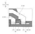
- FIGS. 8A and 8B are diagrams showing an example of a connection structure for connecting the fixed-side metal member 5F and the conductive member CM.
- FIG. 8A is an enlarged view (perspective view) of a range R1 surrounded by broken lines shown in FIG. 3B.
- FIG. 8B is a right side view of range R1 surrounded by broken lines shown in FIG. 3B.
- the base member 18 has a fine dot pattern for clarity.
- the first stationary terminal plate 5F1 is attached to the Y2 side wall (right attachment surface) of the first stationary pedestal portion 18D1 of the base member 18 with a photocurable adhesive.
- the first contact portion CT1 of the first stationary terminal plate 5F1 is joined to the first connection portion ED1 of the first conductive member CM1 via the joining material SD.
- the bonding material SD is given a cross pattern for clarity.
- the second stationary terminal plate 5F2 is attached to the Y2 side wall (right attachment surface) of the first stationary pedestal portion 18D1 of the base member 18 with a photocurable adhesive.
- the second contact portion CT2 of the second stationary terminal plate 5F2 is joined to the second connection portion ED2 of the second conductive member CM2 via the joining material SD.
- the first connection portion ED1 is arranged such that the X1-side (front side) end surface thereof faces the X2-side (rear) end surface of the first contact portion CT1 in the X-axis direction.
- the second connection portion ED2 is arranged such that the X1-side (front) end face faces the X2-side (rear) end face of the second contact portion CT2 in the X-axis direction.
- This arrangement is such that the bonding material SD can adhere to at least the front surface (X1 side surface) of the first connection portion ED1, the rear surface (X2 side surface) and the upper surface (Z1 side surface) of the first contact portion CT1. Therefore, it is possible to increase the strength of connection by the bonding material SD between the first contact portion CT1 and the first connection portion ED1. The same applies to the strength of connection by the bonding material SD between the second contact portion CT2 and the second connection portion ED2.
- this arrangement can prevent the first contact portion CT1 from being joined by the joining material SD to only the right end surface (Y2 side surface) of the first connection portion ED1 which is not plated.
- the right end surface (the surface on the Y2 side) of the first connection portion ED1 is not plated because it is a cut surface formed when cutting off a cut-off connection portion (not shown).
- the truncated connection portion is a portion for connecting a plurality of conductive members, and is used when the plurality of conductive members are embedded in the base member 18 by insert molding, but is finally cut off.
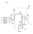
- FIG. 9 is a diagram showing a configuration example of the driving device 10 and the control device 20. As shown in FIG. 9, for the sake of clarity, the parts forming the driving device 10 are represented by solid lines, and the parts forming the control device 20 are represented by dashed lines.
- the driving device 10 is configured to supply a driving current to each of the plurality of shape memory alloy wires SA to drive each of the plurality of shape memory alloy wires SA.
- the drive current is a current for driving (heating and shrinking) the shape memory alloy wire SA, and is, for example, a pulse current.
- the driving device 10 is an electronic circuit configured with active elements AE such as switching elements, operational amplifiers, or ICs, and is configured to operate according to control signals from the control device 20 .
- the drive device 10 includes a first drive device 10A configured to drive the first wire SA1 to the fourth wire SA4, respectively, and a drive device 10A configured to drive the fifth wire SA5 to the eighth wire SA8, respectively. and a second drive device 10B (details not shown).
- the second drive device 10B has the same configuration as the first drive device 10A.
- the control device 20 is configured to be able to control the drive device 10 .
- the control device 20 is a microcomputer including a CPU, a volatile memory device, a nonvolatile memory device, and the like.
- the control device 20 utilizes the driving force along the direction parallel to the optical axis OA due to the contraction of the shape memory alloy wire SA, and the Z1 side (object side) of the image pickup element parallel to the optical axis OA.
- the driving device 10 can be controlled to move the lens holder 2 along the direction.
- the control device 20 can realize an automatic focus adjustment function, which is one of the lens adjustment functions.
- the control device 20 can move the lens holder 2 away from the imaging device to achieve macro photography, and can move the lens holder 2 toward the imaging device to achieve infinity photography.
- the control device 20 can also control the drive device 10 to move the lens holder 2 in the direction intersecting the optical axis OA by controlling the currents flowing through the plurality of shape memory alloy wires SA. Thereby, the control device 20 can realize a camera shake correction function.
- the imaging device 101 having a substantially rectangular parallelepiped shape is mounted on an external substrate (not shown) on which an imaging element (not shown) is mounted.
- the camera module is composed of, for example, an external substrate, an imaging device 101, a lens body attached to the lens holder 2, and an imaging device arranged to face the lens body.
- the driving device 10 and the control device 20 are mounted on an external board. However, at least one of the driving device 10 and the control device 20 may be arranged inside the imaging device 101 . Also, the imaging element may be mounted in the imaging device 101 .
- control device 20 controls the drive device 10 so that the measuring current is supplied to each of the eight shape memory alloy wires SA at a timing different from the timing at which the driving current is supplied. can.
- the measurement current is a current for measuring the resistance between both ends of the shape memory alloy wire SA.
- the current for measurement is desirably a weak current that does not affect the length of the shape memory alloy wire SA, such as a pulse current.
- the control device 20 measures the voltage across the shape memory alloy wire SA when a measurement current having a known magnitude is passed through the shape memory alloy wire SA. The magnitude of the resistance across it (measured resistance) can be derived. Then, the measured resistance value of each of the eight shape memory alloy wires SA is used to realize the desired posture of the lens holder 2 (lens body). For example, the control device 20 can set the target length of each of the eight shape memory alloy wires SA corresponding to the desired posture of the lens holder 2 (lens body).
- the target resistance value of each of the eight shape memory alloy wires SA corresponding to each can be set.
- the control device 20 controls the drive device 10 so that the difference between the measured resistance value of each of the eight shape memory alloy wires SA and the target resistance value approaches zero, so that the lens holder 2 (lens The desired posture of the body) can be realized.
- the current for measurement is a weak current that does not affect the length of the shape memory alloy wire SA, so its magnitude is significantly smaller than the magnitude of the drive current.
- the control device 20 sets a target resistance value for each of the eight shape memory alloy wires SA for realizing a desired posture of the lens holder 2 (lens body). Then, the control device 20 controls the driving device 10 so that the measured resistance value of each of the eight shape memory alloy wires SA becomes the same as the target resistance value. That is, the control device 20 performs feedback control of the resistance values of the eight shape memory alloy wires SA.
- the control device 20 controls the driving device 10 so that the difference between the target resistance value and the measured resistance value approaches zero for each of the eight shape memory alloy wires SA. At least one of the magnitude and supply time (duration) of the driving current supplied to each of the alloy wires SA is adjusted.
- the control device 20 causes the specific shape memory alloy wire SA to contract. Increase the amount of power supplied to the SA.
- the controller 20 lengthens the supply time of the driving current, that is, the time during which a predetermined voltage is applied across the specific shape memory alloy wire SA.
- the controller 20 extends the specific shape memory alloy wire SA so as to stretch the specific shape memory alloy wire SA.
- the amount of power supplied to shape memory alloy wires SA other than the specific shape memory alloy wire SA is increased. For example, the control device 20 lengthens the time during which a predetermined voltage is applied across a shape memory alloy wire SA other than the specific shape memory alloy wire SA.
- the first driving device 10A includes a high potential source 11, a low potential source 12, a constant current source 13, and an active element AE, as shown in FIG.
- the following description with reference to FIG. 9 relates to the first drive 10A, but applies equally to the second drive 10B.
- the high potential source 11 is a potential source configured to have a potential higher than the respective potentials of the ground (GND) and the low potential source 12 .
- the low potential source 12 is a potential source configured to have a potential higher than the ground (GND) potential and lower than the high potential source 11 .
- both the high potential source 11 and the low potential source 12 are fixed in potential, at least one of the high potential source 11 and the low potential source 12 is dynamically changed in potential according to a control signal from the control device 20. may be configured to change to
- the constant current source 13 is an electric circuit that can flow a constant current even if the resistance value of the load changes.
- the constant current source 13 is configured to allow a constant magnitude of measurement current to flow through each of the first wire SA1 to the fourth wire SA4.
- the magnitude of the measurement current is set by the control device 20, for example.
- the magnitude of the current for measurement may be stored in the non-volatile storage device in the control device 20 .
- the magnitude of the measurement current is set based on the results of factory inspections performed at the time of shipment of the product (imaging device 101) so as to be suitable for each of the first wire SA1 to the fourth wire SA4. may have been In this case, variation in characteristics due to individual differences in shape memory alloy wires is suppressed.
- the active element AE is an element that performs active operations such as amplification or rectification with supplied power.
- the active elements AE include a first active element AE1 to a sixth active element AE6.
- the first active element AE1 is a multiplexer that integrates three inputs into one output.
- three inputs of the first active element AE1 are connected to a high potential source 11, a low potential source 12 and a constant current source 13, and one output of the first active element AE1 is connected to the second active element AE2. It is connected to the.
- the second active element AE2 is a demultiplexer that distributes one input to four outputs.
- one input of the second active element AE2 is connected to the first active element AE1
- the four outputs of the second active element AE2 are connected to the first wire SA1, the third wire SA3 and the third active element AE3.
- the fourth active element AE4 is a demultiplexer that distributes one input to four outputs.
- one input of the second active element AE2 is connected to the first active element AE1
- the four outputs of the second active element AE2 are connected to the first wire SA1, the third wire SA3 and the third active element AE3.
- the fourth active element AE4 is a demultiplexer that distributes one input to four outputs.
- the third active element AE3 is a multiplexer that integrates two inputs into one output.
- the two inputs of the third active element AE3 are connected to the second active element AE2 and ground (GND), and one output of the third active element AE3 is connected to the second wire SA2.
- the fourth active element AE4 is a multiplexer that integrates two inputs into one output.
- two inputs of the fourth active element AE4 are connected to the second active element AE2 and ground (GND), and one output of the fourth active element AE4 is connected to the fourth wire SA4.
- the fifth active element AE5 is a switching element that controls the connection between the input and the output.
- the input of the fifth active element AE5 is connected to a common conductive path CD0, which is a conductive path connected to each of the first wire SA1, second wire SA2, third wire SA3, and fourth wire SA4.
- the output of one of the fifth active elements AE5 is connected to ground (GND).
- the sixth active element AE6 is an operational amplifier (operational amplifier) having two inputs and one output.
- one input of the sixth active element AE6 is connected to the first measurement point MP1 on the conductive path between the first active element AE1 and the second active element AE2, and the other input of the sixth active element AE6
- the input is connected to the second measuring point MP2 on the common conductive path CD0 and the output of one of the sixth active elements AE6 is connected to the controller 20.
- the first wire SA1 has one end connected to the second active element AE2 through the first conductive path CD1, and the other end connected to the common conductive path CD0.
- the second wire SA2 has one end connected to the third active element AE3 through the second conductive path CD2, and the other end connected to the common conductive path CD0.
- the third wire SA3 has one end connected to the second active element AE2 through the third conductive path CD3, and the other end connected to the common conductive path CD0.
- the fourth wire SA4 has one end connected to the fourth active element AE4 through the fourth conductive path CD4, and the other end connected to the common conductive path CD0.
- the first conductive path CD1 includes a first stationary terminal plate 5F1
- the second conductive path CD2 includes a second stationary terminal plate 5F2.
- the third conducting path CD3 includes a third stationary terminal plate 5F3
- the fourth conducting path CD4 includes a fourth stationary terminal plate 5F4.
- the common conductive path CD0 includes a first movable-side terminal plate 5M1, a second movable-side terminal plate 5M2, a first leaf spring 6A (third portion 6A3, a fifth portion 6A5, and a second portion 6A2), and a sixth conductive member CM6.
- the first driving device 10A has a first terminal portion TM1, a second terminal portion TM2, a sixth terminal portion TM6, a third contact portion CT3, and a fourth contact portion CT4. Contraction of each of the first wire SA1 to the fourth wire SA4 can be controlled by controlling the voltage applied to each. The same applies to the second driving device 10B.
- the first driving device 10A is used to apply current to each of the first wire SA1 and second wire SA2 when applying current to each of the third wire SA3 and fourth wire SA4.
- a long conductive path (the first conductive member CM1 and the second conductive member CM2 extending along the opening 18K of the base member 18) is not used. Therefore, this configuration reduces the magnetic field (induced magnetic field) formed around the conductive path, which can adversely affect the image quality of the imaging device when currents are passed through the third wire SA3 and the fourth wire SA4.
- this configuration limits the magnitude of the current flowing through each of the third wire SA3 and the fourth wire SA4 more than limiting the magnitude of the current flowing through each of the first wire SA1 and second wire SA2. provide a relaxing effect.
- the first driving device 10A and the second driving device 10B are configured to share the high potential source 11, the low potential source 12, and the constant current source 13, respectively. 11, the low potential source 12, and the constant current source 13 may be provided separately.
- the constant current source 13 includes a first constant current source connected to the first active element AE1 of the first driving device 10A and a first constant current source connected to the first active element (not shown) of the second driving device 10B. 2 constant current sources.
- the driving device 10 is configured to be connected to the high potential source 11 and the low potential source 12 respectively. may be configured to In this case, the other of the high potential source 11 and the low potential source 12 may be omitted.
- the driving device 10 has a constant current source 13, and is configured to electrically connect the constant current source 13 and the shape memory alloy wire SA when the current for measurement is applied to the shape memory alloy wire SA. is configured to However, constant current source 13 may be omitted.
- the driving device 10 may include an AD converter for detecting the magnitude of the measurement current flowing through the shape memory alloy wire SA as a voltage value.
- the driving device 10 may include a shunt resistor for measuring the magnitude of the measuring current flowing through the shape memory alloy wire SA.
- the common conductive path CD0 is configured to be connected to the ground (GND) through the fifth active element AE5, but the high potential source 11 and the low potential source 12 are connected through the active elements. may be configured to be connected to one of In this case, one end of each of the first wire SA1 to the fourth wire SA4 is connected to ground (GND) via an active element such as an N-channel transistor, and the other end is connected to the common conductive path CD0. may be configured.
- 10A to 10D are diagrams showing examples of current paths in the drive device 10, and correspond to FIG. In FIGS. 10A-10D, for clarity, conductive paths through which current is flowing are represented by thick solid lines, and conductive paths through which no current is flowing are represented by dashed lines.
- FIG. 10A shows an example of a path of drive current flowing through two shape memory alloy wires SA (first wire SA1 and second wire SA2) electrically connected in series.
- the path of the drive current shown in FIG. 7A is one specific example of the path of the drive current shown in FIG. 10A.
- FIG. 10A shows that the high potential source 11, the first conductive path CD1, the first wire SA1, the common conductive path CD0, the second wire SA2, the second conductive path CD2, and the ground (GND) are electrically It shows the path of the drive current flowing from the high potential source 11 to the ground (GND) when connected in series.
- the first conductive path CD1 is realized by the first conductive member CM1 and the first fixed terminal plate 5F1 in FIG.
- the second conductive path CD2 is realized by the second fixed terminal plate 5F2 and the second fixed terminal plate 5F2 in FIG. 7A. It is implemented by the conductive member CM2, and the common conductive path CD0 is implemented by the first movable-side terminal plate 5M1.
- FIG. 10B shows an example of the path of the drive current flowing through one shape memory alloy wire SA (first wire SA1).
- the path of the driving current shown in FIG. 7B is one specific example of the path of the driving current shown in FIG. 10B.
- FIG. 10B illustrates the low potential source when the low potential source 12, the first conductive path CD1, the first wire SA1, the common conductive path CD0, and ground (GND) are electrically connected in series.
- 12 shows the path of the drive current flowing from 12 to ground (GND).
- the first conductive path CD1 is realized by the first conductive member CM1 and the first fixed-side terminal plate 5F1 in FIG.
- the common conductive path CD0 is realized by the first movable-side terminal plate 5M1 and the first plate It is realized by the spring 6A (the third portion 6A3, the fifth portion 6A5, and the second portion 6A2) and the sixth conductive member CM6.
- FIG. 10C shows another example of the path of the drive current flowing through one shape memory alloy wire SA (second wire SA2).
- the path of the drive current shown in FIG. 7C is one specific example of the path of the drive current shown in FIG. 10C.
- FIG. 10C illustrates the low potential source when the low potential source 12, the second conductive path CD2, the second wire SA2, the common conductive path CD0, and ground (GND) are electrically connected in series.
- 12 shows the path of the drive current flowing from 12 to ground (GND).
- the second conductive path CD2 is realized by the second conductive member CM2 and the second fixed-side terminal plate 5F2 in FIG.
- the common conductive path CD0 is realized by the first movable-side terminal plate 5M1 and the first plate It is realized by the spring 6A (the third portion 6A3, the fifth portion 6A5, and the second portion 6A2) and the sixth conductive member CM6.
- FIG. 10D shows an example of the path of the current for measurement flowing through one shape memory alloy wire SA (first wire SA1).
- the current path shown in FIG. 7B is one specific example of the current path shown in FIG. 10D.
- FIG. 10D shows the constant current source when the constant current source 13, the first conductive path CD1, the first wire SA1, the common conductive path CD0, and the ground (GND) are electrically connected in series.
- 13 shows the path of the measurement current flowing from 13 to ground (GND).
- the first conductive path CD1 is realized by the first conductive member CM1 and the first fixed-side terminal plate 5F1 in FIG.
- the common conductive path CD0 is realized by the first movable-side terminal plate 5M1 and the first plate It is realized by the spring 6A (the third portion 6A3, the fifth portion 6A5, and the second portion 6A2) and the sixth conductive member CM6.
- one input of the sixth active element AE6 is connected to the first measurement point MP1 on the conductive path between the first active element AE1 and the second active element AE2, and the other input of the sixth active element AE6
- the input is connected to a second measuring point MP2 on the common conductive path CD0. Therefore, the sixth active element AE6 as an operational amplifier outputs to the control device 20 the potential difference (voltage) between the potential at the first measurement point MP1 and the potential at the second measurement point MP2.
- the controller 20 can calculate the resistance of the first wire SA1 based on the magnitude of the voltage and the magnitude of the current output by the constant current source 13.
- the control device 20 can similarly calculate the magnitude of the resistance of each of the second wire SA2 to the fourth wire SA4.
- FIG. 11 is an example of a timing chart of the drive current and the measurement current flowing through the first wire SA1 to the fourth wire SA4. Specifically, FIG. 11 shows the time transition of the voltage applied to each of the first wire SA1 to fourth wire SA4, thereby showing the driving current and It shows the timing relationship of the current for measurement.
- the following description with reference to FIG. 11 relates to the timing relationship between the driving current and the measuring current flowing through the first wire SA1 to the fourth wire SA4. The same applies to the timing relationship of the flowing driving and measuring currents.
- control of the driving device 10 by the control device 20 is realized by the pulse width modulation method.
- control of the driving device 10 by the control device 20 may be realized by other methods such as a pulse amplitude modulation method.
- the controller 20 causes the driving current to flow through the first wires SA1 during the period of the first driving time slot D1, and the driving current to flow through the second wires SA2 during the period of the second driving time slot D2.
- a current flows so that a driving current flows through the third wire SA3 during the period of the third driving time slot D3, and a driving current flows through the fourth wire SA4 during the period of the fourth driving time slot D4. to control the driving device 10.
- the first driving time slot D1 is a time slot set in advance as a period during which the driving current can flow through the first wire SA1.
- the driving device 10 is configured such that the size (duration) of each of the first driving time slot D1 to the fourth driving time slot D4 is the same.
- the drive device 10 may be configured such that the sizes (durations) of the first to fourth drive time slots D1 to D4 are different from each other.
- control device 20 causes the measurement current to flow through the first wire SA1 during the period of the first measurement time slot M1, and causes the measurement current to flow through the second wire SA2 during the period of the second measurement time slot M2.
- the driving device 10 is controlled so that the current for measurement flows through the third wire SA3 during the period of the third measurement time slot M3, and the current for measurement flows through the fourth wire SA4 during the period of the fourth measurement time slot M4. Control.
- the first measurement time slot M1 is a time slot set in advance as a period during which the measurement current can flow through the first wire SA1.
- the drive current is not supplied to each of the first wire SA1 to the fourth wire SA4 during the period of the first measurement time slot M1. Therefore, the period of the first measurement time slot M1 is also called "PWM OFF period" when the pulse width modulation method is adopted.
- the driving device 10 is configured so that the size (duration) of each of the first measurement time slot M1 to the fourth measurement time slot M4 is the same.
- the drive device 10 may be configured such that the sizes (durations) of the first measurement time slot M1 to the fourth measurement time slot M4 are different from each other. Also, in the illustrated example, the duration of the current for measurement is the same as the duration of the time slot for measurement, but it may be shorter or longer than the duration of the time slot for measurement.
- control device 20 controls that the combination of the first drive time slot D1 to the fourth drive time slot D4 and the first measurement time slot M1 constitutes the first drive cycle, A combination of the time slot D1 to the fourth drive time slot D4 and the second measurement time slot M2 constitutes the second drive cycle, and the first drive time slot D1 to the fourth drive time slot D4 and the third measurement.
- the combination of the time slot M3 for driving constitutes the third driving cycle, and the combination of the time slot D1 for driving to the time slot D4 for driving and the time slot M4 for measurement constitutes the fourth driving cycle. Control the drive 10 to configure.
- the control device 20 controls the drive device 10 so that the first measurement time slot M1 is set after the first drive time slot D1 to the fourth drive time slot D4 in the first drive cycle.
- the drive device 10 may be controlled such that the first measurement time slot is set between the two drive time slots.
- the control device 20 may control the drive device 10 so that the first measurement time slot M1 is set between the first drive time slot D1 and the second drive time slot D2. The same applies to the second to fourth drive cycles.
- control device 20 controls the drive device 10 so that a combination of the first drive cycle, the second drive cycle, the third drive cycle, and the fourth drive cycle constitutes one measurement cycle. . That is, the control device 20 is driven so as to acquire the magnitude of resistance of each of the four shape memory alloy wires SA (first wire SA1 to fourth wire SA4) by executing one measurement cycle. Control the device 10 .
- control device 20 controls the drive device 10 so that four drive cycles are executed in the order of the first drive cycle, the second drive cycle, the third drive cycle, and the fourth drive cycle.
- the drive 10 may be controlled such that the four drive cycles are performed in other orders.
- the control device 20 controls the drive device 10 so as to obtain the magnitude of the resistance of one shape memory alloy wire SA when executing one drive cycle.
- the driving device 10 may be controlled so as to acquire the magnitude of resistance of two or more shape memory alloy wires SA when executing one driving cycle.
- the first drive cycle may be composed of a combination of the first drive time slot D1 to the fourth drive time slot D4, the first measurement time slot M1, and the second measurement time slot M2.
- the second measurement time slot M2 in the second drive cycle may be omitted.
- the first driving time slot D1 of the first driving cycle starts at time t1, the first driving time slot D1 ends and the second driving time slot D2 starts at time t2, and the time t3.
- the second driving time slot D2 ends and the third driving time slot D3 begins at time t4, the third driving time slot D3 ends and the fourth driving time slot D4 begins at time t5, and the fourth driving time slot D3 ends at time t5.
- the first measurement time slot D4 ends and the first measurement time slot M1 begins, and at time t6 the first measurement time slot M1 ends and the first drive time slot D1 of the second drive cycle begins.
- the control device 20 drives so that the drive current flows through the first wire SA1 for the same duration E1 as the duration of the first drive time slot D1. Control the device 10 .
- the control device 20 causes the drive current to flow through the second wire SA2 for a duration E2 shorter than the duration of the second drive time slot D2. It controls the driving device 10 .
- the control device 20 causes the driving current to flow through the third wire SA3 for a duration E3 shorter than the duration of the third driving time slot D3. It controls the driving device 10 .
- the control device 20 causes the drive current to flow through the fourth wire SA4 for a duration E4 shorter than the duration of the fourth drive time slot D4. It controls the driving device 10 . Further, in the first measurement time slot M1 of the first drive cycle, the control device 20 drives so that the measurement current flows through the first wire SA1 for the same duration E5 as the duration of the first measurement time slot M1. Control the device 10 .
- the duration E5 during which the measurement current flows through the first wire SA1 is set, for example, according to the conversion speed of the AD converter for converting the analog signal output by the sixth active element AE6 as an operational amplifier into a digital signal.
- the duration E5 can be set shorter as the conversion speed of the AD converter is faster. In other words, if the control device 20 sets the duration E5 longer, that is, if the measurement time is set longer, even if an AD converter with a slow conversion speed is used, the four shape memory alloy wires SA can accurately obtain the resistance of
- the duration E1 of the drive current flowing through the first wire SA1 is determined by the conversion speed of the AD converter. Must be set to be longer than the minimum duration.
- the first drive time slot D1 and the first measurement time slot M1 are set separately, so the duration E1 does not necessarily have to be equal to or longer than the duration E5. That is, the control device 20 can adopt a duration time E1 that is shorter than the duration time E5 during which the current for measurement flows through the first wire SA1. The same applies to the second wire SA2 to the fourth wire SA4.
- the driving device 10 drives the first driving device 10A configured to drive the first wire SA1 to the fourth wire SA4, respectively, and the fifth wire SA5 to the eighth wire SA8, respectively. and a second drive unit 10B configured to allow. That is, the imaging device 101 is configured to include two drive devices capable of driving the four shape memory alloy wires SA. Compared to a configuration having only one driving device capable of driving eight shape memory alloy wires SA, this configuration increases the drive time slot that can be assigned to one shape memory alloy wire SA, It is possible to reduce the magnitude of the current when a desired amount of power is supplied to the shape memory alloy wire SA, thereby reducing the magnetic field formed around the conductive path.
- the imaging device 101 may be configured to include only one driving device capable of driving the eight shape memory alloy wires SA.
- the controller 20 configures one measurement cycle with eight drive cycles, and one drive cycle with a combination of eight drive time slots and one measurement time slot.
- the single drive may be controlled as follows.
- the imaging device 101 may be configured to include four drive devices capable of driving two shape memory alloy wires SA, and eight drive devices capable of driving one shape memory alloy wire SA. It may be configured to have one.
- the control device 20 controls the drive device 10 so that the drive current is supplied to one shape memory alloy wire SA in one drive time slot.
- the drive device 10 may be controlled such that drive currents are simultaneously supplied to a plurality of shape memory alloy wires SA in a time slot. Even if a driving current is simultaneously supplied to a plurality of shape memory alloy wires SA in one driving time slot, the driving time slot and the measurement time slot are separated. This is because the resistance value of each shape memory alloy wire SA can be accurately measured. Specifically, in a configuration in which the resistance value of a shape memory alloy wire is measured while a drive current is being supplied to the shape memory alloy wire, the drive current (measurement current) is applied to a plurality of shape memory alloy wires simultaneously.
- FIG. 12A shows the first conductive member CM1 forming part of the first conductive path CD1 (see FIG. 9) and the second conductive member CM2 forming part of the second conductive path CD2 (see FIG. 9). It is a perspective view.
- FIG. 12B is another example of a timing chart of the driving current and the measuring current flowing through the first wire SA1 to the fourth wire SA4, and corresponds to FIG. Specifically, FIG.
- FIG. 12B shows the temporal transition of the voltage applied to each of the first wire SA1 to fourth wire SA4, thereby showing the driving current flowing through each of first wire SA1 to fourth wire SA4 and It shows the timing relationship of the current for measurement. Note that the following description with reference to FIG. 12A relates to the current flowing through each of the first conductive member CM1 and the second conductive member CM2, but the same applies to the current flowing through each of the third conductive member CM3 and the fourth conductive member CM4. Applies to Further, the following description with reference to FIGS.
- 12A and 12B relates to the timing relationship between the driving current and the measuring current flowing through the first wire SA1 to the fourth wire SA4, respectively, but the fifth wire SA5 to the eighth wire SA8 The same applies to the timing relationship of the driving and measuring currents flowing through each of the .
- control device 20 causes the driving current to flow through each of the first wire SA1 and the second wire SA2 during the combined period of the first driving time slot D1 and the second driving time slot D2.
- the driving device 10 is controlled such that the driving current flows through the third wire SA3 and the fourth wire SA4 during the combined period of the third driving time slot D3 and the fourth driving time slot D4.
- control device 20 controls the first wire SA1 and the second wire SA2 for a period from time t1 to time td, that is, a duration E11 that is shorter than the duration of the first driving time slot D1.
- the driving device 10 is controlled so that the driving current flows.
- the control device 20 connects the high potential source 11, the first conductive path CD1, the first wire SA1, the common conductive path CD0, the second wire SA2, and the second conductive path CD2.
- the ground (GND) is electrically connected in series, and the driving device 10 is controlled so that relatively large currents are simultaneously supplied to the first wire SA1 and the second wire SA2. That is, the control device 20 causes a current to flow from the first point PT1 to the second point PT2 of the first conductive path CD1 (the first conductive member CM1) as indicated by an arrow AR61 in FIG. 12A.
- the driving device 10 is controlled such that current flows from the second point PT12 to the first point PT11 of the second conductive path CD2 (second conductive member CM2).
- first mode the operation mode of the driving device 10 at this time
- strong driving state the state of the imaging device 101 at this time.
- This state is also called a “common drive state” because the first wire SA1 and the second wire SA2 are driven at the same time.
- control device 20 causes the drive device 10 to execute the "first mode” that realizes the "common drive state", so that the pulse width modulation method is adopted as compared to the case where the "first mode” is not executed. This has the effect of lengthening the "PWM OFF period" when
- control device 20 controls either the first wire SA1 or the second wire SA2 for driving during the remaining period of the combined period of the first driving time slot D1 and the second driving time slot D2.
- a current flows, and the driving current flows only through either the third wire SA3 or the fourth wire SA4 during the remaining period of the combined period of the third driving time slot D3 and the fourth driving time slot D4.
- the driving device 10 is controlled as follows.
- control device 20 causes the driving current to flow only through the first wire SA1 over a period from time td to time te, that is, a duration E12 shorter than the duration of the first driving time slot D1.
- the driving device 10 is controlled to flow.
- the controller 20 electrically connects the low potential source 12, the first conductive path CD1, the first wire SA1, the common conductive path CD0, and the ground (GND) in series.
- the driving device 10 is controlled so that a relatively small current is supplied to the first wire SA1. That is, the control device 20 allows current to flow from the first point PT1 to the second point PT2 of the first conductive path CD1 (the first conductive member CM1), as indicated by an arrow AR61 in FIG. 12A, and The driving device 10 is controlled so that no current flows through CD2 (second conductive member CM2).
- the operation mode of the driving device 10 at this time will be referred to as a "second mode”
- the state of the imaging device 101 at this time will be referred to as a "weak driving state” or a "first weak driving state”.
- the amount of power supplied to the first wire SA1 in the "strong drive state” of the first drive cycle and the amount of power supplied to the first wire SA1 in the "first weak drive state” of the first drive cycle corresponds to the amount of power supplied to the first wire SA1 when the high potential source 11 and the first wire SA1 are connected for the duration of the first driving time slot D1.
- the dotted line indicates the voltage waveform when the high-potential source 11 and the first wire SA1 are connected for the duration of the first driving time slot D1.
- the magnitude of the current flowing through the first conductive path CD1 (first conductive member CM1) is smaller than in the "strong drive state”.
- the magnitude of the magnetic field formed around the first conductive member CM1) is also reduced.
- no current is supplied to the second conductive path CD2 (second conductive member CM2), and a magnetic field that cancels the magnetic field formed around the first conductive path CD1 (first conductive member CM1) is generated.
- the magnetic field (induced magnetic field) that can adversely affect the image quality of the imaging device is reduced by the amount of the current flowing through the first conductive path CD1 (first conductive member CM1). reduced.
- control device 20 operates during the remaining period of the combined period of the first driving time slot D1 and the second driving time slot D2, that is, the first driving time slot D1 and the second driving time slot D2.
- the driving device 10 may be controlled so that the driving current flows only through the second wire SA2.
- the controller 20 electrically connects the low potential source 12, the second conductive path CD2, the second wire SA2, the common conductive path CD0, and the ground (GND) in series.
- the driving device 10 may be controlled so that the second wire SA2 is connected and a relatively small current is supplied to the second wire SA2. That is, the control device 20 controls that the current flows from the first point PT11 to the second point PT12 of the second conductive path CD2 (second conductive member CM2) and the current flows to the first conductive path CD1 (first conductive member CM1).
- the driving device 10 may be controlled so that the current does not flow.
- the operation mode of the drive device 10 at this time will be referred to as a "third mode”
- the state of the imaging device 101 at this time will be referred to as a "weak drive state” or a "second weak drive state”.
- control device 20 causes the driving device 10 to execute the "first mode” and the "second mode” during the combined period of the first driving time slot D1 and the second driving time slot D2. Later, the driving device 10 may be controlled to execute the "third mode".
- the control device 20 controls the driving device so that the driving current flows only through the second wire SA2 over a period from time tf to time tg, that is, a duration E13 shorter than the duration of the second driving time slot D2. 10 may be controlled. For example, it is for fine adjustment of the amount of power supplied to the second wire SA2.
- FIG. 12B shows the voltage waveform with a dotted line when the low potential source 12 and the second wire SA2 are connected over the period from time tf to time tg.
- the driving device 10 may be configured to execute a combination of the "first mode", the "second mode” and the "third mode”.
- the state of the imaging device 101 when the drive device 10 is caused to execute the “second mode” or the “third mode” is “individually driven” because the first wires SA1 or the second wires SA2 are individually driven. Also called “state”.
- the control device 20 causes the driving device 10 to execute a composite mode in which the “first mode” and the “second mode” or the “third mode” are combined so that the four shape memory alloy wires SA (first wire A desired amount of power can be supplied to each of SA1 to fourth wire SA4).
- the "first mode" for the first wire SA1 and the second wire SA2 is more effective as the amount of power to be supplied to the first wire SA1 and the amount of power to be supplied to the second wire SA2 are larger and the difference between them is smaller. can be. This is because a large amount of electric power can be supplied to each of the first wires SA1 and the second wires SA2 in a short period of time while suppressing adverse effects on the image quality of the imaging device.
- the control device 20 can reduce the adverse effect on the image quality of the imaging device by increasing the duration of the "second mode” or the "third mode” as much as possible.
- the current flowing through the first conductive path CD1 (first conductive member CM1) or the second conductive path CD2 (second conductive member CM2) can be reduced, and the first conductive path CD1 (first conductive member CM1) or the second conductive path CD2 This is because the magnetic field formed around (the second conductive member CM2) can be reduced.
- control device 20 when causing the driving device 10 to execute the "second mode", the control device 20 connects the low potential source 12 having a fixed potential and the first wire SA1 as shown in FIG. 10B. is controlled so that the drive device 10 is connected.
- control device 20 may be configured such that a variable potential source having an adjustable potential is connected to first wire SA1 when causing drive device 10 to execute the “second mode”.
- the controller 20 increases the duration E12 to the duration E12a while making the potential of the variable potential source smaller than the potential of the low potential source 12, thereby connecting the low potential source 12 and the first wire SA1.
- the driving device 10 may be controlled so that the same amount of power is supplied to the first wire SA1 as the amount of power supplied to the first wire SA1 when the first wire SA1 is supplied. That is, the control device 20 may lengthen the duration E12a as much as possible in order to make the potential of the variable potential source as low as possible.
- FIG. 12B shows the voltage waveform with a dotted line when the variable potential source and the first wire SA1 are connected for the duration E12a.
- the state of the imaging device 101 at this time is called a “variable weak drive state”. In this "variable weak drive state”, the magnitude of the current flowing through the first conductive path CD1 (first conductive member CM1) is smaller than in the "first weak drive state”. The magnitude of the magnetic field formed around the first conductive member CM1) is further reduced. The same applies when the driving device 10 is caused to execute the "third mode".
- the change in the magnitude of the potential of the variable potential source is desirably performed so that the change cycle is sufficiently long with respect to the cycle of the measurement cycle.
- the change is synchronous with the measurement cycle.
- the change is such that one measurement cycle consisting of a first drive cycle, a second drive cycle, a third drive cycle, and a fourth drive cycle is executed and the four shape memory alloy wires SA (first It may be performed each time the resistance value of each of the wires SA1 to SA4) is obtained.
- the change may be made during the fourth measurement time slot M4.
- FIG. 13 is a diagram showing another configuration example of the driving device 10.
- the following description with reference to FIG. 13 relates to the first drive device 10A configured to drive the first wire SA1 to the fourth wire SA4, respectively, but the fifth wire SA5 to the eighth wire SA8 are respectively driven.
- FIG. 13 for the sake of clarity, illustration of the configuration of active elements and the like for estimating the resistance values of the first wires SA1 to the fourth wires SA4 is omitted. Configuration is connected.
- the first drive device 10A shown in FIG. 13 differs from the first drive device 10A shown in FIG. 9 in that it includes five active elements AE (tenth active element AE10 to fourteenth active element AE14).
- the tenth active element AE10 controls connection between the common conductive path CD0 connected to the other ends of the first wires SA1 to the fourth wires SA4 and either one of the low potential source (LOW) and the ground (GND). It is a switching element that
- the eleventh active element AE11 is a switching element that controls connection between the first conductive path CD1 connected to one end of the first wire SA1 and either a high potential source (HIGH) or a low potential source (LOW). .
- the twelfth active element AE12 is a switching element that controls connection between the second conductive path CD2 connected to one end of the second wire SA2 and the ground (GND).
- the thirteenth active element AE13 is a switching element that controls connection between the third conductive path CD3 connected to one end of the third wire SA3 and either a high potential source (HIGH) or a low potential source (LOW). .
- the fourteenth active element AE14 is a switching element that controls the connection between the fourth conductive path CD4 connected to one end of the fourth wire SA4 and the ground (GND).
- the control device 20 connects the high potential source (HIGH), the first conductive path CD1, the first wire SA1, the common conductive path CD0, the second wire SA2, and the ground (GND) electrically in series.
- the controller 20 also controls the tenth active element so that the low potential source (LOW), the first conductive path CD1, the first wire SA1, the common conductive path CD0, and the ground (GND) are electrically connected in series.
- a relatively small current can be supplied only to the first wire SA1 by controlling the AE10 and the eleventh active element AE11.
- the controller 20 also controls the tenth active element so that the low potential source (LOW), the common conductive path CD0, the second wire SA2, the second conductive path CD2, and the ground (GND) are electrically connected in series.
- LOW low potential source
- COM common conductive path
- CD0 common conductive path
- CD2 second conductive path
- GND ground
- control device 20 is such that the high potential source (HIGH), the third conductive path CD3, the third wire SA3, the common conductive path CD0, the fourth wire SA4, and the ground (GND) are electrically connected in series.
- the thirteenth active element AE13 and the fourteenth active element AE14 in such a manner, relatively large currents can be simultaneously supplied to the third wire SA3 and the fourth wire SA4.
- the controller 20 also controls the tenth active element so that the low potential source (LOW), the third conductive path CD3, the third wire SA3, the common conductive path CD0, and the ground (GND) are electrically connected in series.
- LOW low potential source
- LOW low potential source
- LOW low potential source
- the third conductive path CD3, the third wire SA3, the common conductive path CD0, and the ground (GND) are electrically connected in series.
- AE10 and the thirteenth active element AE13 a relatively small current can be supplied only to the third wire SA3.
- the controller 20 also controls the tenth active element so that the low potential source (LOW), the common conductive path CD0, the fourth wire SA4, the fourth conductive path CD4, and the ground (GND) are electrically connected in series.
- LOW low potential source
- AE10 and fourteenth active element AE14 a relatively small current can be supplied only to fourth wire SA4.
- the potential of the high potential source (HIGH) is fixed, but the potential may be dynamically changed according to the control signal from the control device 20.
- the low potential source (LOW) is configured such that the potential dynamically changes according to the control signal from the control device 20, but the potential may be fixed.
- the common conductive path CD0 to which the other ends of the first wires SA1 to the fourth wires SA4 are connected, is connected to a potential source having a potential of 3V or the like.
- One end of each of the wires SA1 to SA4 may be selectively connected to the ground (GND) via an active element such as an N-channel transistor.
- the driving device 10 can execute a combined mode combining the "first mode” and the "second mode” or “third mode”. Further, the driving device 10 can execute a composite mode in which the "first mode", the "second mode” and the “third mode” are combined. Further, the driving device 10 can supply the measuring current to each of the eight shape memory alloy wires SA at a timing different from the timing at which the driving current is supplied.
- the imaging device 101 includes a fixed side member FB including the base member 18 as a fixed base and a lens holder 2 capable of holding a lens body, as shown in FIG. a movable-side member MB provided movably with respect to the fixed-side member FB; and one end fixed to the fixed-side member FB and the other end fixed to the movable-side member MB to move the movable-side member MB. and a driving device 10 (see FIG. 9) capable of driving each of the plurality of shape memory alloy wires SA by supplying a driving current to each of the plurality of shape memory alloy wires SA. , and a control device 20 (see FIG.
- the control device 20 controls the driving device 10 so that the measurement current is supplied to each of the plurality of shape memory alloy wires SA at a timing different from the timing at which the driving current is supplied, thereby obtaining a plurality of shapes. It is configured to acquire the resistance value (measured resistance value) of the memory alloy wire SA.
- the control device 20 is configured to be able to set the target length (target resistance value) of each of the eight shape memory alloy wires SA corresponding to the desired orientation of the lens holder 2 (lens body). Then, the control device 20 controls the drive device 10 so that the difference between the measured resistance value of each of the eight shape memory alloy wires SA and the target resistance value approaches zero, thereby making the lens holder 2 (lens body) It is configured to be able to realize the desired posture of. In addition, the controller 20 increases the amount of electric power supplied to one specific shape memory alloy wire SA, thereby contracting the one specific shape memory alloy wire SA and reducing its measured resistance value. be able to.
- This configuration has the effect of more accurately estimating the length of the shape memory alloy wire SA. This is because in this configuration, the time during which the measurement current is continued to be supplied is set independently of the time during which the drive current is continued to be supplied. That is, in this configuration, the time during which the measurement current is continued to be supplied is set to a necessary and sufficient length.
- this configuration includes an AD converter for detecting the voltage across the shape memory alloy wire SA in order to derive the resistance value of the shape memory alloy wire SA
- the operating speed of the AD converter can be set lower. That is, it brings about the effect of making it possible to use a relatively inexpensive AD converter.
- the measuring current is supplied to the shape memory alloy wire SA at a timing different from the timing of supplying the driving current. It is for
- control device 20 may control the drive device 10 so as to supply drive currents to the plurality of shape memory alloy wires SA at different timings.
- This configuration brings about the effect that the expansion and contraction of each of the plurality of shape memory alloy wires SA can be controlled more accurately.
- This configuration can prevent part of the drive current to be supplied to a specific shape memory alloy wire SA from being supplied to another shape memory alloy wire SA.
- control device 20 may control the drive device 10 so as to supply the current for measurement to each of the plurality of shape memory alloy wires SA at different timings.
- This configuration has the effect of enabling more accurate acquisition of the resistance value of each of the plurality of shape memory alloy wires SA.
- This configuration can prevent part of the current for measurement that should be supplied to a specific shape memory alloy wire SA from being supplied to another shape memory alloy wire SA.
- control device 20 determines that the minimum value of the time for continuously supplying the drive current to each of the plurality of shape memory alloy wires SA is the measurement current to each of the plurality of shape memory alloy wires SA.
- the driving device 10 may be controlled to be shorter than the continuous supply time.
- This configuration has the effect of making it possible to more flexibly adjust the time during which the supply of the driving current continues.
- This configuration is because the time during which the drive current is continuously supplied can be made shorter than the time during which the measurement current is continuously supplied. It should be noted that shortening the time during which the driving current is continuously supplied means that the amount of electric power supplied to one specific shape memory alloy wire SA in one driving cycle (driving time slot) can be reduced, that is, , means that the shape memory alloy wire SA can be slightly heated to cause the shape memory alloy wire SA to contract slightly.
- control device 20 may control the driving device 10 so that the magnitude of the current for measurement is smaller than the magnitude of the current for driving.
- This configuration has the effect of reducing the influence of the current for measurement on driving the shape memory alloy wire SA.
- the control device 20 supplies the driving current once to each of the plurality of shape memory alloy wires SA, and measures one of the plurality of shape memory alloy wires SA.
- the driving device 10 may be controlled to supply the electric current.
- the control device 20 may control the drive device 10 to supply the current for measurement to each of the plurality of shape memory alloy wires SA by repeating the drive cycle a plurality of times.
- This configuration brings about the effect that the lens holder 2 (lens body) can be driven more smoothly. This is because the drive current can be supplied to each of the plurality of shape memory alloy wires SA at relatively short intervals. In addition, it is possible to prevent the period in which the drive current cannot be supplied to one of the plurality of shape memory alloy wires SA from becoming excessively long.
- control device 20 controls the driving device 10 so as to supply the current for measurement to each of the plurality of shape memory alloy wires SA by repeating the driving cycle the same number of times as the number of the plurality of shape memory alloy wires SA.
- This configuration has the effect of suppressing a decrease in control response speed and enabling the lens holder 2 (lens body) to be driven more smoothly. This is because the current for measurement can be supplied to each of the plurality of shape memory alloy wires SA at relatively short intervals. In addition, it is possible to prevent the period in which the current for measurement cannot be supplied to one of the plurality of shape memory alloy wires SA from becoming excessively long.
- the driving device 10 supplies a driving current to each of the four shape memory alloy wires (the first wire SA1 to the fourth wire SA4) to supply the four shape memory alloy wires (the first wire SA1 to the fourth wire SA4). 4 wires SA4), and another four shape memory alloy wires (fifth wire SA5 to eighth wire SA8), each of which is supplied with a driving current to drive another four wires SA4). and a second driving device 10B capable of driving each of the shape memory alloy wires (fifth wire SA5 to eighth wire SA8).
- This configuration has the effect of shortening the time required for one drive cycle. That is, this configuration brings about an effect of being able to suppress a decrease in control response speed.
- a drive current is supplied to each of the eight shape memory alloy wires (first wire SA1 to eighth wire SA8) to provide eight shape memory alloy wires (first wire SA1 to eighth wire SA8).
- first wire SA1 to eighth wire SA8 to provide eight shape memory alloy wires (first wire SA1 to eighth wire SA8).
- the duration of the time slot for measurement can be lengthened without increasing the time required for one driving cycle. Therefore, in this configuration, it is not necessary to increase the applied voltage when supplying the drive current to the shape memory alloy wire SA in order to lengthen the duration of the measurement time slot. As a result, this configuration can suppress the influence of noise caused by increasing the applied voltage on the image.
- the imaging apparatus 101 includes a fixed side member FB including a base member 18 as a fixed base and a lens body capable of holding a lens body facing the imaging element.
- a movable member MB including the lens holder 2 and movable with respect to the fixed member FB, and a first shape memory alloy wire having one end fixed to the fixed member FB and the other end fixed to the movable member MB. and a second wire SA2 as a second shape memory alloy wire having one end fixed to the fixed side member FB and the other end fixed to the movable side member MB, and the base member 18 provided with A first conductive path CD1 (see FIG.
- a portion connecting the first point PT1 and the second point PT2 on the first conductive path CD1 (first conductive member CM1) and a second conductive path CD2 (second conductive member CM2 ) are installed so as to be parallel to each other on the base member 18 .
- a first point PT1 on the first conductive path CD1 (first conductive member CM1) is arranged in parallel with a first point PT11 on the second conductive path CD2 (second conductive member CM2).
- a second point PT2 on the path CD1 (first conductive member CM1) is arranged in parallel with a second point PT12 on the second conductive path CD2 (second conductive member CM2).
- the driving device 10 electrically connects the first conducting path CD1, the first wire SA1, the common conducting path CD0, the second wire SA2, and the second conducting path CD2 in series.
- a current is supplied to the first wire SA1 and the second wire SA2, and the current flows from the first point PT1 to the second point PT2 of the first conductive path CD1 (first conductive member CM1) as indicated by an arrow AR61 in FIG. flows and current flows from the second point PT12 to the first point PT11 of the second conductive path CD2 (second conductive member CM2) as indicated by an arrow AR62 in FIG.
- the first conductive path CD1, the first wire SA1, and the common conductive path CD0 are electrically connected in series to supply a current to the first wire SA1 to form the first conductive path CD1 (first conductive path).
- a second mode in which a current flows through the member CM1), and a second wire SA2, SA2, and common conductive path CD0, which are electrically connected in series as shown in FIG. 10C. It is configured to be switchable between a third mode in which current is supplied to SA2 and current flows through the second conductive path CD2 (second conductive member CM2).
- the imaging apparatus 101 is configured to be able to execute a combination of the first mode and at least one of the second mode and the third mode.
- This configuration has the effect of reducing the magnitude of the magnetic field formed around the conductive path for supplying current to the shape memory alloy wire SA. Therefore, this configuration has the effect of reducing noise to the imaging device caused by the magnetic field formed around the conducting path.
- the driving device 10 has a first conducting path CD1 (first conducting member CM1) and a second conducting path CD2 (second This is because currents flow in opposite directions in each of the conductive members CM2), and the magnitude of the current flowing through the first conductive path CD1 (first conductive member CM1) This is because it is the same as the magnitude of the current flowing through the second conductive member CM2).
- the driving device 10 is configured to execute a combined mode in which at least one of the first mode, the second mode, and the third mode is combined, the first wire SA1 and the second wire SA2 each have A desired amount of power can be supplied accurately.
- the combination of the first mode and at least one of the second mode and the third mode is a combination of the first mode and the second mode, a combination of the first mode and the third mode, or a combination of the first mode and the third mode. It is a combination of the 2nd mode and the 3rd mode.
- any operation mode may be executed first, or each operation mode may be executed continuously, A time slot for measurement or a PWM OFF period may be inserted between each operation mode.
- a combined mode combining the first mode and at least one of the second mode and the third mode may be executed during one or more drive cycles, and one or more measurement cycles. may be performed during the
- the driving device 10 may be configured such that the magnitude of the current flowing in the first mode is larger than the magnitude of the current flowing in each of the second mode and the third mode.
- This configuration has the effect of further reducing the magnetic field (induced magnetic field) that can adversely affect the image quality of the imaging device.
- the magnetic field formed by the current flowing through the first conductive path CD1 (first conductive member CM1) and the magnetic field formed by the current flowing through the second conductive path CD2 (second conductive member CM2) cancel each other out. It's for mutual interaction.
- the greater the magnitude of the current flowing in the first mode the greater the magnitude of the current flowing in the second mode executed after the first mode. This is because the smaller the magnitude of the current flowing in the second mode, the smaller the magnetic field formed by the current flowing through the first conductive path CD1 (first conductive member CM1) in the second mode.
- the larger the magnitude of the current flowing in the first mode the greater the magnitude of the current flowing in the third mode executed after the first mode. This is because the smaller the magnitude of the current flowing in the third mode, the smaller the magnetic field formed by the current flowing through the second conductive path CD2 (second conductive member CM2) in the third mode. .
- the portion connecting the two points PT 12 may be embedded in the base member 18 .
- This configuration has the effect of further reducing the magnetic field (induced magnetic field) that can adversely affect the image quality of the imaging device. of the magnetic field formed around the portion of the first conductive member CM1 embedded in the base member 18 and the magnetic field formed around the portion of the second conductive member CM2 embedded in the base member 18 This is because propagation to each imaging element is at least partially suppressed by the base member 18 .
- first wire SA1 and the second wire SA2 may be arranged side by side in plan view along the optical axis direction (Z-axis direction), as shown in FIG. 4B.
- first wire SA1 and the second wire SA2 are arranged substantially perpendicular to the respective extending directions (X-axis direction) of the first wire SA1 and the second wire SA2 and in the optical axis direction (Z-axis direction).
- X-axis direction extending directions
- Z-axis direction optical axis direction
- they may be arranged so as to cross each other.
- This configuration has the effect of further reducing the net magnetic field (induced magnetic field) that can adversely affect the image quality of the imaging device.
- the induced magnetic field formed around the first wires SA1 and the second wires SA2 This is because the induced magnetic field formed around it cancels each other out.
- the base member 18 has a first side portion 18E1, a second side portion 18E2, a third side portion 18E3, and a third side portion 18E3 in plan view along the optical axis direction (Z-axis direction). It may have the shape of a rectangular frame having a fourth side portion 18E4. Then, as shown in FIG. 12A, the first conductive path CD1 (see FIG. 9) may include the first terminal portion TM1, and the second conductive path CD2 (see FIG. 9) may include the second terminal portion TM2.
- first terminal portion TM1 and the second terminal portion TM2 are connected to the third side which is one of the first side portion 18E1, the second side portion 18E2, the third side portion 18E3, and the fourth side portion 18E4. It may be arranged in the portion 18E3.
- the portion connecting the PT11 and the second point PT12 is the second side portion 18E2 which is another one of the first side portion 18E1, the second side portion 18E2, the third side portion 18E3, and the fourth side portion 18E4. may be arranged in parallel along the
- This configuration has the effect of facilitating the mounting of the imaging device. This is because a flexible printed circuit board or the like connected to the imaging element can be arranged under the second side portion 18E2 of the base member 18. FIG.
- the current for measurement is supplied to each of the plurality of shape memory alloy wires SA at a timing different from the timing at which the current for driving is supplied.
- the control device 20 has a step of controlling the drive device 10 and obtaining the resistance values of the plurality of shape memory alloy wires SA.
- the imaging device 101 can more accurately estimate the length of the shape memory alloy wire SA. This is because in this control method, the time during which the measurement current is continued to be supplied is set independently of the time during which the drive current is continued to be supplied. That is, in this control method, the time during which the measurement current is continued to be supplied is set to a necessary and sufficient length.
- the control method of the imaging device 101 includes a first conducting path CD1, a first wire SA1, a common conducting path CD0, a second wire SA2, and a second conducting path CD2. are electrically connected in series to supply a current to the first wire SA1 and the second wire SA2, and as shown in FIG. A first mode in which a current flows to the second point PT2 and a current flows from the second point PT12 to the first point PT11 of the second conductive path CD2 (the second conductive member CM2), and as shown in FIG.
- the imaging device 101 can reduce the magnitude of the magnetic field formed around the conductive paths for supplying current to the shape memory alloy wires SA. Therefore, the imaging device 101 can reduce noise to the imaging device caused by the magnetic field formed around the conductive path.
- Lens holder 2D Movable side pedestal part 2D1... First movable side pedestal part 2D2... Second movable side pedestal part 2P... Cylindrical part 2S... Protruding part 2S1 ⁇ ... First projecting part 2S2... Second projecting part 2T... Projecting part 2V... Projecting part 4... Cover member 4A... Peripheral wall part 4A1... First side plate part 4A2 ... second side plate portion 4A3... third side plate portion 4A4... fourth side plate portion 4B... top plate portion 4K... opening 4S... storage portion 5... metal member 5F... ⁇ Fixed side metal member 5F1... First fixed side terminal plate 5F2... Second fixed side terminal plate 5F3... Third fixed side terminal plate 5F4...
- First leaf spring 6A1 ... ⁇ First part 6A2...Second part 6A3...Third part 6A4...Fourth part 6A5...Fifth part 6AH1...First through hole 6AH2...Second through hole 6AH3- 3rd through hole 6AH4 4th through hole 6AH5 5th through hole 6AH6 6th through hole 6B 2nd plate spring 6B1 1st part 6B2 3rd Second part 6B3... Third part 6B4... Fourth part 6B5... Fifth part 6BH1... First through hole 6BH2... Second through hole 6BH3...
- Fourth wire SA5... Fifth wire SA6... Sixth wire SA7... Seventh wire SA8... Eighth wire SD Joining material TM1... First terminal part TM2... 2nd terminal section TM3... 3rd terminal section TM4... 4th terminal section TM5... 5th terminal section TM6... 6th terminal section
Landscapes
- Physics & Mathematics (AREA)
- General Physics & Mathematics (AREA)
- Engineering & Computer Science (AREA)
- Chemical & Material Sciences (AREA)
- Combustion & Propulsion (AREA)
- Optics & Photonics (AREA)
- Mechanical Engineering (AREA)
- General Engineering & Computer Science (AREA)
- Multimedia (AREA)
- Signal Processing (AREA)
- Lens Barrels (AREA)
- Studio Devices (AREA)
- Adjustment Of Camera Lenses (AREA)
Abstract
Description
Claims (7)
- 固定基台を含む固定側部材と、
撮像素子に対向するようにレンズ体を保持可能なレンズホルダを含む、前記固定側部材に対して移動可能な可動側部材と、
一端が前記固定側部材に固定されるとともに他端が前記可動側部材に固定される第1形状記憶合金ワイヤと、
一端が前記固定側部材に固定されるとともに他端が前記可動側部材に固定される第2形状記憶合金ワイヤと、
前記固定基台に設けられて前記第1形状記憶合金ワイヤの一端に電気的に接続される第1導電路と、
前記固定基台に設けられて前記第2形状記憶合金ワイヤの一端に電気的に接続される第2導電路と、
前記第1形状記憶合金ワイヤ及び前記第2形状記憶合金ワイヤのそれぞれの他端に電気的に接続される共通導電路と、
前記第1導電路、前記第2導電路、及び前記共通導電路のそれぞれに電気的に接続できるように構成され、前記第1形状記憶合金ワイヤ及び前記第2形状記憶合金ワイヤのそれぞれに電流を供給して前記第1形状記憶合金ワイヤ及び前記第2形状記憶合金ワイヤのそれぞれを駆動可能な駆動装置と、を備え、
前記第1導電路上の第1点と第2点とを繋ぐ部分、及び、前記第2導電路上の第1点と第2点とを繋ぐ部分は、前記固定基台において互いに並行するように設置されており、
前記第1導電路上の第1点は、前記第2導電路上の第1点に並設されており、
前記第1導電路上の第2点は、前記第2導電路上の第2点に並設されており、
前記駆動装置は、
前記第1導電路と前記第1形状記憶合金ワイヤと前記共通導電路と前記第2形状記憶合金ワイヤと前記第2導電路とを電気的に直列に接続させて前記第1形状記憶合金ワイヤ及び前記第2形状記憶合金ワイヤに電流を供給して前記第1導電路の第1点から第2点に電流が流れ且つ前記第2導電路の第2点から第1点に電流が流れるようにする第1モードと、
前記第1導電路と前記第1形状記憶合金ワイヤと前記共通導電路とを電気的に直列に接続させて前記第1形状記憶合金ワイヤに電流を供給して前記第1導電路に電流が流れるようにする第2モードと、
前記第2導電路と前記第2形状記憶合金ワイヤと前記共通導電路とを電気的に直列に接続させて前記第2形状記憶合金ワイヤに電流を供給して前記第2導電路に電流が流れるようにする第3モードと、
を切り換えできるように構成されており、且つ、
前記第1モードと、前記第2モード及び前記第3モードの少なくとも一方とを組み合わせて実行するように構成されていることを特徴とする撮像装置。 - 前記第1モードで流れる電流の大きさは、前記第2モード及び前記第3モードのそれぞれで流れる電流の大きさよりも大きい、
請求項1に記載の撮像装置。 - 前記第1導電路上の第1点と第2点とを繋ぐ部分と前記第2導電路上の第1点と第2点とを繋ぐ部分とは前記固定基台に埋設されている、
請求項1又は請求項2に記載の撮像装置。 - 前記第1形状記憶合金ワイヤ及び前記第2形状記憶合金ワイヤは、光軸方向に沿って見た平面視において並ぶように配置されており、且つ、前記第1形状記憶合金ワイヤ及び前記第2形状記憶合金ワイヤのそれぞれの延在方向に略垂直で且つ光軸方向に垂直な方向に沿って見た側面視において、互いに交差するように配置されている、
請求項1乃至請求項3の何れかに記載の撮像装置。 - 前記固定基台は、光軸方向に沿って見た平面視において、第1辺部、第2辺部、第3辺部、及び第4辺部を有する矩形枠の形状を有し、
前記第1導電路は、第1端子部を含み、
前記第2導電路は、第2端子部を含み、
前記第1端子部と前記第2端子部とは、前記第1辺部、前記第2辺部、前記第3辺部、及び前記第4辺部のうちの一つに配設されており、
前記第1導電路上の第1点と第2点とを繋ぐ部分と前記第2導電路上の第1点と第2点とを繋ぐ部分とは、前記第1辺部、前記第2辺部、前記第3辺部、及び前記第4辺部のうちの別の一つに沿って並行するように配置されている、
請求項1乃至請求項4の何れかに記載の撮像装置。 - 前記レンズ体と、
請求項1乃至請求項5の何れかに記載の撮像装置と、
を含む、カメラモジュール。 - 固定基台を含む固定側部材と、撮像素子に対向するようにレンズ体を保持可能なレンズホルダを含む、前記固定側部材に対して移動可能な可動側部材と、一端が前記固定側部材に固定されるとともに他端が前記可動側部材に固定される第1形状記憶合金ワイヤと、一端が前記固定側部材に固定されるとともに他端が前記可動側部材に固定される第2形状記憶合金ワイヤと、前記固定基台に設けられて前記第1形状記憶合金ワイヤの一端に電気的に接続される第1導電路と、前記固定基台に設けられて前記第2形状記憶合金ワイヤの一端に電気的に接続される第2導電路と、前記第1形状記憶合金ワイヤ及び前記第2形状記憶合金ワイヤのそれぞれの他端に電気的に接続される共通導電路と、前記第1導電路、前記第2導電路、及び前記共通導電路のそれぞれに電気的に接続できるように構成され、前記第1形状記憶合金ワイヤ及び前記第2形状記憶合金ワイヤのそれぞれに電流を供給して前記第1形状記憶合金ワイヤ及び前記第2形状記憶合金ワイヤのそれぞれを駆動可能な駆動装置と、を備える撮像装置の制御方法であって、
前記第1導電路上の第1点と第2点とを繋ぐ部分、及び、前記第2導電路上の第1点と第2点とを繋ぐ部分は、前記固定基台において互いに並行するように設置されており、
前記第1導電路上の第1点は、前記第2導電路上の第1点に並設されており、
前記第1導電路上の第2点は、前記第2導電路上の第2点に並設されており、
前記撮像装置の制御方法は、前記第1導電路と前記第1形状記憶合金ワイヤと前記共通導電路と前記第2形状記憶合金ワイヤと前記第2導電路とを電気的に直列に接続させて前記第1形状記憶合金ワイヤ及び前記第2形状記憶合金ワイヤに電流を供給して前記第1導電路の第1点から第2点に電流が流れ且つ前記第2導電路の第2点から第1点に電流が流れるようにする第1モードと、前記第1導電路と前記第1形状記憶合金ワイヤと前記共通導電路とを電気的に直列に接続させて前記第1形状記憶合金ワイヤに電流を供給して前記第1導電路に電流が流れるようにする第2モード、及び、前記第2導電路と前記第2形状記憶合金ワイヤと前記共通導電路とを電気的に直列に接続させて前記第2形状記憶合金ワイヤに電流を供給して前記第2導電路に電流が流れるようにする第3モードの少なくとも一方と、を組み合わせた複合モードを前記駆動装置に実行させるステップを有する、
ことを特徴とする撮像装置の制御方法。
Priority Applications (4)
| Application Number | Priority Date | Filing Date | Title |
|---|---|---|---|
| JP2023574079A JP7698072B2 (ja) | 2022-01-17 | 2023-01-12 | 撮像装置、カメラモジュール、及び撮像装置の制御方法 |
| CN202380016795.2A CN118556208A (zh) | 2022-01-17 | 2023-01-12 | 摄像装置、相机模块以及摄像装置的控制方法 |
| US18/768,514 US20240361670A1 (en) | 2022-01-17 | 2024-07-10 | Imaging apparatus, camera module, and control method for imaging apparatus |
| JP2025098500A JP2025120424A (ja) | 2022-01-17 | 2025-06-12 | 撮像装置、カメラモジュール、及び撮像装置の制御方法 |
Applications Claiming Priority (2)
| Application Number | Priority Date | Filing Date | Title |
|---|---|---|---|
| JP2022-005275 | 2022-01-17 | ||
| JP2022005275 | 2022-01-17 |
Related Child Applications (1)
| Application Number | Title | Priority Date | Filing Date |
|---|---|---|---|
| US18/768,514 Continuation US20240361670A1 (en) | 2022-01-17 | 2024-07-10 | Imaging apparatus, camera module, and control method for imaging apparatus |
Publications (1)
| Publication Number | Publication Date |
|---|---|
| WO2023136306A1 true WO2023136306A1 (ja) | 2023-07-20 |
Family
ID=87279210
Family Applications (1)
| Application Number | Title | Priority Date | Filing Date |
|---|---|---|---|
| PCT/JP2023/000662 Ceased WO2023136306A1 (ja) | 2022-01-17 | 2023-01-12 | 撮像装置、カメラモジュール、及び撮像装置の制御方法 |
Country Status (4)
| Country | Link |
|---|---|
| US (1) | US20240361670A1 (ja) |
| JP (2) | JP7698072B2 (ja) |
| CN (1) | CN118556208A (ja) |
| WO (1) | WO2023136306A1 (ja) |
Citations (3)
| Publication number | Priority date | Publication date | Assignee | Title |
|---|---|---|---|---|
| US20180149142A1 (en) * | 2015-05-26 | 2018-05-31 | Cambridge Mechatronics Limited | Assembly method for a shape memory alloy actuator arrangement |
| JP2019525048A (ja) * | 2016-06-09 | 2019-09-05 | ハッチンソン テクノロジー インコーポレイテッドHutchinson Technology Incorporated | サスペンションアセンブリについての接着剤を有する形状記憶合金ワイヤ取付構造体 |
| WO2021023150A1 (zh) * | 2019-08-07 | 2021-02-11 | 华为技术有限公司 | 马达、摄像头模组及终端设备 |
Family Cites Families (3)
| Publication number | Priority date | Publication date | Assignee | Title |
|---|---|---|---|---|
| AU3114299A (en) * | 1999-03-26 | 2000-10-16 | R. Sjhon Minners | Bistable micro-switch and method of manufacturing the same |
| JP2010051056A (ja) * | 2008-08-19 | 2010-03-04 | Fujinon Corp | 駆動装置及び光学装置 |
| WO2010140382A1 (ja) * | 2009-06-04 | 2010-12-09 | 株式会社ニコン | レンズユニットおよび撮像装置 |
-
2023
- 2023-01-12 WO PCT/JP2023/000662 patent/WO2023136306A1/ja not_active Ceased
- 2023-01-12 CN CN202380016795.2A patent/CN118556208A/zh active Pending
- 2023-01-12 JP JP2023574079A patent/JP7698072B2/ja active Active
-
2024
- 2024-07-10 US US18/768,514 patent/US20240361670A1/en active Pending
-
2025
- 2025-06-12 JP JP2025098500A patent/JP2025120424A/ja active Pending
Patent Citations (3)
| Publication number | Priority date | Publication date | Assignee | Title |
|---|---|---|---|---|
| US20180149142A1 (en) * | 2015-05-26 | 2018-05-31 | Cambridge Mechatronics Limited | Assembly method for a shape memory alloy actuator arrangement |
| JP2019525048A (ja) * | 2016-06-09 | 2019-09-05 | ハッチンソン テクノロジー インコーポレイテッドHutchinson Technology Incorporated | サスペンションアセンブリについての接着剤を有する形状記憶合金ワイヤ取付構造体 |
| WO2021023150A1 (zh) * | 2019-08-07 | 2021-02-11 | 华为技术有限公司 | 马达、摄像头模组及终端设备 |
Also Published As
| Publication number | Publication date |
|---|---|
| JP7698072B2 (ja) | 2025-06-24 |
| CN118556208A (zh) | 2024-08-27 |
| JP2025120424A (ja) | 2025-08-15 |
| US20240361670A1 (en) | 2024-10-31 |
| JPWO2023136306A1 (ja) | 2023-07-20 |
Similar Documents
| Publication | Publication Date | Title |
|---|---|---|
| US9479699B2 (en) | Shape memory alloy actuation apparatus | |
| CN104982028B (zh) | 控制sma致动装置的方法、系统及sma致动装置 | |
| KR101932795B1 (ko) | 형상 기억 합금 작동 장치 | |
| CN108292074B (zh) | 对sma致动装置的控制 | |
| JP3759508B2 (ja) | アクチュエータ及びアクチュエータ駆動方法並びにアクチュエータシステム | |
| EP2261507A1 (en) | Shape memory alloy actuation apparatus | |
| JP7143288B2 (ja) | 可動要素を調整するためのアクチュエータ、使用方法、及び調整方法 | |
| CN101668947A (zh) | 形状记忆合金驱动设备 | |
| CN101416090A (zh) | 照相机镜头驱动设备 | |
| WO2008129290A1 (en) | Control circuits for an sma actuator | |
| Kazi et al. | SMA actuator for optical image stabilization | |
| JP7698072B2 (ja) | 撮像装置、カメラモジュール、及び撮像装置の制御方法 | |
| JP2023104347A (ja) | 撮像装置、カメラモジュール、及び撮像装置の制御方法 | |
| JP7295921B2 (ja) | レンズ駆動装置及びカメラモジュール | |
| CN117460994A (zh) | 生成用于驱动sma装置的驱动信号的方法 | |
| JP7533906B2 (ja) | カメラモジュール | |
| GB2612116A (en) | SMA actuator assembly | |
| Coppoolse et al. | Dual-axis single-mirror mechanism for beam steering and stabilisation in optical inter satellite links | |
| JP7597455B2 (ja) | レンズ駆動装置及びカメラモジュール | |
| CN114391119A (zh) | 透镜驱动装置及相机模块 | |
| CN114527546B (zh) | 透镜驱动装置以及相机模块 | |
| JP7518969B2 (ja) | 撮像素子駆動装置及びカメラモジュール | |
| CN114460789B (zh) | 透镜驱动装置以及相机模块 | |
| JP7556640B2 (ja) | モジュール駆動装置及び光学装置 | |
| CN114026492A (zh) | 透镜驱动装置、相机模块及透镜驱动装置的制造方法 |
Legal Events
| Date | Code | Title | Description |
|---|---|---|---|
| 121 | Ep: the epo has been informed by wipo that ep was designated in this application |
Ref document number: 23740314 Country of ref document: EP Kind code of ref document: A1 |
|
| WWE | Wipo information: entry into national phase |
Ref document number: 2023574079 Country of ref document: JP |
|
| WWE | Wipo information: entry into national phase |
Ref document number: 202380016795.2 Country of ref document: CN |
|
| NENP | Non-entry into the national phase |
Ref country code: DE |
|
| 122 | Ep: pct application non-entry in european phase |
Ref document number: 23740314 Country of ref document: EP Kind code of ref document: A1 |