WO2023136256A1 - 面発光装置、および表示装置 - Google Patents
面発光装置、および表示装置 Download PDFInfo
- Publication number
- WO2023136256A1 WO2023136256A1 PCT/JP2023/000407 JP2023000407W WO2023136256A1 WO 2023136256 A1 WO2023136256 A1 WO 2023136256A1 JP 2023000407 W JP2023000407 W JP 2023000407W WO 2023136256 A1 WO2023136256 A1 WO 2023136256A1
- Authority
- WO
- WIPO (PCT)
- Prior art keywords
- layer
- light
- sealing member
- resin
- led
- Prior art date
- Legal status (The legal status is an assumption and is not a legal conclusion. Google has not performed a legal analysis and makes no representation as to the accuracy of the status listed.)
- Ceased
Links
Images





Classifications
-
- G—PHYSICS
- G02—OPTICS
- G02F—OPTICAL DEVICES OR ARRANGEMENTS FOR THE CONTROL OF LIGHT BY MODIFICATION OF THE OPTICAL PROPERTIES OF THE MEDIA OF THE ELEMENTS INVOLVED THEREIN; NON-LINEAR OPTICS; FREQUENCY-CHANGING OF LIGHT; OPTICAL LOGIC ELEMENTS; OPTICAL ANALOGUE/DIGITAL CONVERTERS
- G02F1/00—Devices or arrangements for the control of the intensity, colour, phase, polarisation or direction of light arriving from an independent light source, e.g. switching, gating or modulating; Non-linear optics
- G02F1/01—Devices or arrangements for the control of the intensity, colour, phase, polarisation or direction of light arriving from an independent light source, e.g. switching, gating or modulating; Non-linear optics for the control of the intensity, phase, polarisation or colour
- G02F1/13—Devices or arrangements for the control of the intensity, colour, phase, polarisation or direction of light arriving from an independent light source, e.g. switching, gating or modulating; Non-linear optics for the control of the intensity, phase, polarisation or colour based on liquid crystals, e.g. single liquid crystal display cells
- G02F1/133—Constructional arrangements; Operation of liquid crystal cells; Circuit arrangements
- G02F1/1333—Constructional arrangements; Manufacturing methods
- G02F1/1335—Structural association of cells with optical devices, e.g. polarisers or reflectors
- G02F1/1336—Illuminating devices
- G02F1/133602—Direct backlight
- G02F1/133606—Direct backlight including a specially adapted diffusing, scattering or light controlling members
-
- G—PHYSICS
- G02—OPTICS
- G02F—OPTICAL DEVICES OR ARRANGEMENTS FOR THE CONTROL OF LIGHT BY MODIFICATION OF THE OPTICAL PROPERTIES OF THE MEDIA OF THE ELEMENTS INVOLVED THEREIN; NON-LINEAR OPTICS; FREQUENCY-CHANGING OF LIGHT; OPTICAL LOGIC ELEMENTS; OPTICAL ANALOGUE/DIGITAL CONVERTERS
- G02F1/00—Devices or arrangements for the control of the intensity, colour, phase, polarisation or direction of light arriving from an independent light source, e.g. switching, gating or modulating; Non-linear optics
- G02F1/01—Devices or arrangements for the control of the intensity, colour, phase, polarisation or direction of light arriving from an independent light source, e.g. switching, gating or modulating; Non-linear optics for the control of the intensity, phase, polarisation or colour
- G02F1/13—Devices or arrangements for the control of the intensity, colour, phase, polarisation or direction of light arriving from an independent light source, e.g. switching, gating or modulating; Non-linear optics for the control of the intensity, phase, polarisation or colour based on liquid crystals, e.g. single liquid crystal display cells
- G02F1/133—Constructional arrangements; Operation of liquid crystal cells; Circuit arrangements
- G02F1/1333—Constructional arrangements; Manufacturing methods
- G02F1/1335—Structural association of cells with optical devices, e.g. polarisers or reflectors
- G02F1/1336—Illuminating devices
- G02F1/133602—Direct backlight
- G02F1/133603—Direct backlight with LEDs
-
- H—ELECTRICITY
- H10—SEMICONDUCTOR DEVICES; ELECTRIC SOLID-STATE DEVICES NOT OTHERWISE PROVIDED FOR
- H10H—INORGANIC LIGHT-EMITTING SEMICONDUCTOR DEVICES HAVING POTENTIAL BARRIERS
- H10H20/00—Individual inorganic light-emitting semiconductor devices having potential barriers, e.g. light-emitting diodes [LED]
- H10H20/80—Constructional details
- H10H20/85—Packages
- H10H20/852—Encapsulations
- H10H20/854—Encapsulations characterised by their material, e.g. epoxy or silicone resins
-
- H—ELECTRICITY
- H10—SEMICONDUCTOR DEVICES; ELECTRIC SOLID-STATE DEVICES NOT OTHERWISE PROVIDED FOR
- H10H—INORGANIC LIGHT-EMITTING SEMICONDUCTOR DEVICES HAVING POTENTIAL BARRIERS
- H10H20/00—Individual inorganic light-emitting semiconductor devices having potential barriers, e.g. light-emitting diodes [LED]
- H10H20/80—Constructional details
- H10H20/85—Packages
- H10H20/855—Optical field-shaping means, e.g. lenses
-
- H—ELECTRICITY
- H10—SEMICONDUCTOR DEVICES; ELECTRIC SOLID-STATE DEVICES NOT OTHERWISE PROVIDED FOR
- H10H—INORGANIC LIGHT-EMITTING SEMICONDUCTOR DEVICES HAVING POTENTIAL BARRIERS
- H10H20/00—Individual inorganic light-emitting semiconductor devices having potential barriers, e.g. light-emitting diodes [LED]
- H10H20/80—Constructional details
- H10H20/85—Packages
- H10H20/857—Interconnections, e.g. lead-frames, bond wires or solder balls
-
- H—ELECTRICITY
- H10—SEMICONDUCTOR DEVICES; ELECTRIC SOLID-STATE DEVICES NOT OTHERWISE PROVIDED FOR
- H10H—INORGANIC LIGHT-EMITTING SEMICONDUCTOR DEVICES HAVING POTENTIAL BARRIERS
- H10H29/00—Integrated devices, or assemblies of multiple devices, comprising at least one light-emitting semiconductor element covered by group H10H20/00
- H10H29/10—Integrated devices comprising at least one light-emitting semiconductor component covered by group H10H20/00
- H10H29/14—Integrated devices comprising at least one light-emitting semiconductor component covered by group H10H20/00 comprising multiple light-emitting semiconductor components
- H10H29/142—Two-dimensional arrangements, e.g. asymmetric LED layout
-
- H—ELECTRICITY
- H10—SEMICONDUCTOR DEVICES; ELECTRIC SOLID-STATE DEVICES NOT OTHERWISE PROVIDED FOR
- H10H—INORGANIC LIGHT-EMITTING SEMICONDUCTOR DEVICES HAVING POTENTIAL BARRIERS
- H10H29/00—Integrated devices, or assemblies of multiple devices, comprising at least one light-emitting semiconductor element covered by group H10H20/00
- H10H29/80—Constructional details
- H10H29/85—Packages
- H10H29/852—Encapsulations
- H10H29/854—Encapsulations characterised by their material, e.g. epoxy or silicone resins
-
- H—ELECTRICITY
- H10—SEMICONDUCTOR DEVICES; ELECTRIC SOLID-STATE DEVICES NOT OTHERWISE PROVIDED FOR
- H10H—INORGANIC LIGHT-EMITTING SEMICONDUCTOR DEVICES HAVING POTENTIAL BARRIERS
- H10H29/00—Integrated devices, or assemblies of multiple devices, comprising at least one light-emitting semiconductor element covered by group H10H20/00
- H10H29/80—Constructional details
- H10H29/85—Packages
- H10H29/855—Optical field-shaping means, e.g. lenses
-
- H—ELECTRICITY
- H10—SEMICONDUCTOR DEVICES; ELECTRIC SOLID-STATE DEVICES NOT OTHERWISE PROVIDED FOR
- H10W—GENERIC PACKAGES, INTERCONNECTIONS, CONNECTORS OR OTHER CONSTRUCTIONAL DETAILS OF DEVICES COVERED BY CLASS H10
- H10W90/00—Package configurations
Definitions
- the present disclosure relates to surface emitting devices and display devices using the same.
- a display device using a light-emitting diode element is attracting attention and is being developed because of its advantages of high brightness and high contrast.
- backlights using light-emitting diode elements are being developed as backlights used in liquid crystal display devices.
- the backlight is also called a mini-LED backlight (in the following description, "light-emitting diodes” may be referred to as "LEDs").
- LED backlights are broadly classified into a direct type and an edge light type.
- Edge-light type LED backlights are usually used in small and medium-sized display devices such as mobile terminals such as smartphones, but direct type LED backlights are often used from the viewpoint of brightness. being considered.
- direct type LED backlights are often used from the viewpoint of brightness. being considered.
- large-sized display devices such as large-screen liquid crystal televisions, in many cases, a direct type LED backlight is used.
- a direct type LED backlight has a structure in which a plurality of LED elements are arranged on a substrate.
- a direct type LED backlight by independently controlling a plurality of LED elements, the brightness of each area of the LED backlight is adjusted according to the brightness of the displayed image, so-called local dimming is realized. be able to. As a result, it is possible to significantly improve the contrast and reduce the power consumption of the display device.
- FIG. 12(a) shows a conventional LED backlight 60 in which pins 65 are arranged in order to secure the distance d between the LED elements 63 on the support substrate 62 and the diffusion member 66.
- FIG. 12(b1) shows a conventional LED backlight 61 in which spacers 67 are arranged between a support substrate 62 and a diffusion member 66, and
- FIG. 12(b2) is a schematic plan view of the spacers 67.
- the LED elements used in the above-mentioned LED backlights are so-called bare chips that are not protected by a sealing material or the like because of the need for higher definition of image quality and the demand for thinner display devices. (hereinafter sometimes referred to as an LED bare chip) may be used.
- the present disclosure has been made in view of the above problems, and a main object thereof is to provide a surface emitting device with good light extraction efficiency even when LED bare chips are used.
- the inventors of the present invention conducted intensive studies and found that the decrease in the light extraction efficiency of the bare chip is due to the fact that the transparent base material such as sapphire used for the bare chip has a relatively high refractive index.
- the refractive index difference between the transparent base material and the surrounding air becomes large, and as a result, the light emitted from the light-emitting layer is reflected at the interface between the transparent base material and the surrounding air, resulting in a high reflectance.
- the inventors have found that the light extraction efficiency is lowered, and have completed the present invention.
- the present disclosure includes a support substrate, a light emitting diode substrate having a light emitting diode element arranged on one side of the supporting substrate, and a light emitting diode substrate arranged on the surface of the light emitting diode substrate on the side of the light emitting diode element, a sealing member for sealing a diode element, wherein the light emitting diode element includes a transparent base material made of an inorganic material and a light emitting layer formed on one side surface of the transparent base material. and the transparent substrate is exposed on the surface, and the sealing member is in contact with the surface of the transparent substrate opposite to the surface on which the light emitting layer is formed and the side surface. and the sealing member has a haze value of 4% or more and a thickness greater than that of the light emitting diode element.
- the present disclosure also provides a display device including a display panel and the above-described surface emitting device arranged on the back surface of the display panel.
- the present disclosure has the effect of being able to provide a surface light-emitting device with good light extraction efficiency even when an LED bare chip is used in a surface light-emitting device used in a display device or the like.
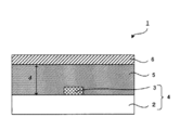
- FIG. 1 is a schematic cross-sectional view illustrating a surface emitting device according to the present disclosure
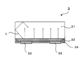
- FIG. 1 is a schematic cross-sectional view showing an example of an LED bare chip in the present disclosure
- FIG. FIG. 4 is a process diagram showing an example of a method of forming a sealing member according to the present disclosure
- FIG. 2 is a schematic cross-sectional view illustrating the structure of the sealing member of the surface emitting device according to the present disclosure
- FIG. 4 is a schematic cross-sectional view showing an example of a second diffusion member
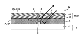
- FIG. 4 is a schematic cross-sectional view showing an example of a surface emitting device including a second diffusion member in the present disclosure
- 5 is a graph illustrating transmitted light intensity distribution
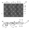
- FIG. 4A is a schematic plan view and a cross-sectional view showing an example of a first embodiment of a reflective structure of a second diffusion member
- FIG. 9A is a schematic plan view and a cross-sectional view showing an example of a second embodiment of the reflecting structure of the second diffusion member
- FIG. 11 is a schematic cross-sectional view showing another example of the second aspect of the reflective structure of the second diffusion member
- 1 is a schematic diagram showing an example of a display device of the present disclosure
- FIG. 1 is a schematic cross-sectional view of a conventional LED backlight
- a surface light emitting device includes a light emitting diode substrate having a supporting substrate and light emitting diode elements arranged on one surface side of the supporting substrate, and a surface of the light emitting diode substrate facing the light emitting diode elements.
- a sealing member arranged to seal the light emitting diode element, wherein the light emitting diode element is formed on one side of the transparent substrate made of an inorganic material; and a light-emitting layer formed on the surface of the transparent substrate, the sealing member comprising a surface of the transparent substrate opposite to the surface on which the light-emitting layer is formed, and The sealing member is in contact with the side surface, has a haze value of 4% or more, and is thicker than the light emitting diode element.
- FIG. 1 is a schematic cross-sectional view showing an example of the surface emitting device of the present disclosure.
- a surface emitting device 1 includes a support substrate 2, an LED substrate 4 having an LED bare chip 3 arranged on one side of the support substrate 2, and an LED substrate 4 on the LED bare chip 3 side. It has a sealing member 5 that is arranged on the surface side and seals the LED elements 3 , and a diffusion member 6 that is arranged on the surface side of the sealing member 5 opposite to the LED substrate 4 side.
- the sealing member 5 in the present disclosure has a haze value of 4% or more and a thickness d greater than the thickness of the LED element 3 .
- the LED bare ship 3 includes a transparent base material 31 made of sapphire or the like, a light emitting layer 32 formed on the transparent base material 31, electrodes 33, 33 for conducting electricity to the light emitting layer, and a passivation layer 34 that protects the light emitting layer 33 .
- the sealing member 5 is formed so as to be in contact with the surface of the transparent base material 31 opposite to the surface on which the light emitting layer 32 is formed, and the side surface.
- the side and top surfaces of the LED bare chip are in contact with the air.
- the light L emitted from the light-emitting layer 32 is reflected by the side surface of the transparent base material 31 made of sapphire or the like, depending on the direction of light emission from the light-emitting layer 32.
- the light is also reflected in the light-emitting layer 32 and finally absorbed in the light-emitting surface of the light-emitting layer 32 or the like. For this reason, in such a surface emitting device, a problem may arise in light extraction efficiency from the LED bare chip.
- the sealing member 5 is arranged so as to be in contact with the surface of the transparent substrate 31 opposite to the surface on which the light-emitting layer 32 is formed, that is, the upper surface and the side surface of the transparent substrate 31.
- the difference in refractive index between the transparent base material 31 and the material constituting the transparent base material 31 is reduced compared to the case where the transparent base material 31 is in contact with the air.
- the surface emitting device of the present disclosure it is possible to improve the light extraction efficiency from the light emitting layer 32 .
- Each configuration of the surface emitting device of the present disclosure will be described below.
- the LED substrate in the present disclosure is a member having a supporting substrate and a plurality of LED elements arranged on one side of the supporting substrate.
- the LED element has a transparent base material made of an inorganic material and a light-emitting layer formed on one side of the transparent base material, and a bare chip in which the transparent base material is exposed on the surface (hereinafter referred to as , LED bare chips.).
- the LED bare chip used in the present disclosure is a member arranged on one side of the support substrate and functions as a light source.
- Such an LED bare chip can include, for example, those illustrated in FIG. becomes. Light emitted from the light-emitting layer is emitted to the outside through the transparent base material.
- the transparent base material used for the above LED bare chip is not particularly limited as long as it is usually composed of an inorganic material, but crystal growth of the material constituting the light emitting layer described later is possible.
- Specific examples include sapphire (Al 2 O 3 ), silicon carbide, and silicon. Among them, sapphire is preferably used.
- the lower limit of the refractive index of the transparent substrate used in the present disclosure is usually 1.4 or higher, preferably 1.5 or higher.
- the upper limit of the refractive index of the transparent substrate is usually 2.5 or less, preferably 2.0 or less. This is because the above-described problems arise in the case of a transparent substrate made of a material having a refractive index within the above range.
- the refractive index of the transparent base material As a method for measuring the refractive index of the transparent base material, it can be measured by an Abbe refractometer.
- the shape of the transparent substrate is usually rectangular parallelepiped or cylindrical, but the surface on which the light-emitting layer is not formed may be shaped so as to reduce the reflectance.
- the surface of the transparent base material in the present disclosure opposite to the surface on which the light-emitting layer is formed (sometimes referred to as the top surface) and the side surface of the transparent base material are in contact with a sealing member, which will be described later.
- the upper surface of the transparent base material and the sealing member are in contact with each other over the entire surface.
- the side surface of the transparent base material and the sealing member are not particularly limited as long as they are in contact with each other. It is preferable that they are in contact with each other.
- the ratio of the area where the transparent base material is in contact with the sealing member is measured by the following method. First, ten LED bare chips covered with the sealing member are cut out from the surface emitting device. Next, the LED bare chip covered with the sealing member is cut using a microtome. The transparent substrate of the cut LED bare chip is observed with a scanning electron microscope (SEM) to determine the coverage with the sealing member. Let the average value of the determined coverage ratio be the ratio of the area where the transparent base material is in contact with the sealing member.
- SEM scanning electron microscope
- the light-emitting layer used in the above LED bare chip is not particularly limited as long as it is a material usually used in LED bare chips.
- Gallium arsenide phosphide, gallium phosphide, zinc selenide, aluminum gallium indium phosphide and the like can be mentioned.
- an LED bare chip is used as the form of the LED element as in the present disclosure, for example, a blue light emitting layer, an ultraviolet light emitting layer, or an infrared light emitting layer can be used as the light emitting layer. This is because white light can be emitted by using it in combination with a wavelength conversion member.
- a blue light-emitting layer for example, can be combined with a yellow phosphor, or combined with red and green phosphors to produce white light.
- the ultraviolet emitting layer can generate white light by combining with, for example, a red phosphor, a green phosphor, and a blue phosphor.
- the light-emitting layer of the LED bare chip is a blue light-emitting layer. This is because the surface emitting device of the present disclosure can irradiate white light with high brightness.
- an electrode a protective layer (passivation layer), etc. are usually disposed on the LED bare chip.
- the LED bare chips are usually arranged at regular intervals on one side of a support substrate, which will be described later.
- the transparent base material is arranged on the side opposite to the support substrate. That is, they are arranged in the order of the support substrate, and if necessary, the electrodes, the light-emitting layer, and the transparent substrate.
- the size and arrangement density of the LED bare chips are appropriately selected according to the application and size of the surface emitting device of the present disclosure.
- the lower limit of the length of one side is preferably 0.01 mm or more, more preferably 0.05 mm or more, and particularly preferably 0.05 mm or more. It is preferably 1 mm or more.
- the upper limit of the length of one side is preferably 2 mm or less, more preferably 1 mm or less, and particularly preferably 0.5 mm or less.
- the maximum diameter is preferably within the above range.
- the LED bare chips Due to the small size of the LED bare chips, the LED bare chips can be arranged at high density, that is, the intervals (pitch) between the LED bare chips can be reduced, and the distance between the LED substrate and the diffusion member can be shortened, that is, the sealing member can be reduced. This is because the thickness can be reduced. This makes it possible to reduce the thickness and weight of the device.
- the support substrate used in the present disclosure is a member that supports the LED bare chip, the sealing member, the diffusion member, and the like.
- the support substrate may be transparent or opaque. Moreover, the support substrate may have flexibility or may have rigidity.
- the material of the support substrate may be an organic material, an inorganic material, or a composite material obtained by combining both an organic material and an inorganic material.
- a resin substrate can be used as the support substrate.
- a ceramic substrate or a glass substrate can be used as the support substrate.
- a glass epoxy substrate can be used as the support substrate.
- a metal core substrate for example, can also be used as the support substrate.
- a printed circuit board on which a circuit is formed by printing can also be used as the support substrate.
- the thickness of the support substrate is not particularly limited, and is appropriately selected according to the presence or absence of flexibility or rigidity, the application and size of the surface emitting device of the present disclosure, and the like.
- the LED substrate in the present disclosure is not particularly limited as long as it has the above-described supporting substrate and LED bare chip, and can have any necessary configuration as appropriate. Examples of such a configuration include a wiring portion, a terminal portion, an insulating layer, a reflective layer, a heat radiating member, and the like. Each configuration can be the same as that used for known LED substrates.
- the wiring part is electrically connected to the LED bare chip.
- the wiring part is usually arranged in a pattern.
- the wiring portion can be arranged on the supporting substrate via an adhesive layer.
- a material for the wiring portion for example, a metal material, a conductive polymer material, or the like can be used.
- the wiring part is electrically connected by a joint corresponding to the electrode of the LED bare chip.
- a bonding agent or solder having a conductive material such as a metal or a conductive polymer can be used.
- a reflective layer can be arranged on the surface of the support substrate on which the LED bare chips are arranged and in areas other than the LED bare chip mounting area.
- the light reflected by the second layer of the diffusing member can be reflected by the reflective layer of the support substrate and made to enter the first layer of the diffusing member again, thereby increasing the light utilization efficiency.
- the reflective layer can be similar to reflective layers commonly used in LED substrates.
- the reflective layer includes a white resin film containing metal particles, inorganic particles or a pigment and a resin, a metal film, a porous film, and the like.
- the thickness of the reflective layer is not particularly limited as long as the desired reflectance is obtained, and is set as appropriate.
- a method for forming the LED substrate can be the same as a known forming method.
- the sealing member in the present disclosure has a haze value of 4% or more and is thicker than the LED element.
- the sealing member has optical transparency and is arranged on the light emitting surface side of the LED substrate.
- the haze value of the sealing member in the present disclosure is 4% or more, preferably 8% or more, more preferably 10% or more, particularly 12% or more is preferably
- the upper limit is not particularly limited, but is, for example, 85% or less, preferably 60% or less, more preferably 30% or less.
- the haze value is a value for the entire sealing member, and the sealing member is cut out from the surface emitting device and measured using a haze meter (HM-150, manufactured by Murakami Color Research Laboratory) according to JIS K7136:2000. It can be measured by a method according to
- the method for adjusting the haze value for obtaining the haze value described above is not particularly limited, but includes a method using the degree of crystallinity of the resin, a method of changing the content of fine particles in the resin, and the like. Among them, the method of adjusting the crystallinity of the resin is preferable. This is because when the haze value is increased by increasing the crystallinity of the resin, it is possible to obtain the effect of reducing the rectilinear transmitted light.
- the thickness of the sealing member in the present disclosure may be any thickness as long as it is thicker than the LED element, specifically preferably 50 ⁇ m or more, more preferably 80 ⁇ m or more, and particularly preferably 200 ⁇ m. That's it.
- the thickness of the sealing member is preferably 800 ⁇ m or less, more preferably 750 ⁇ m or less, and particularly preferably 700 ⁇ m or less.
- the "thickness" in this specification can be measured using a known measuring method capable of measuring a size on the order of ⁇ m. Specifically, a contact-type film thickness measuring device (Mitutoyo Thickness Gauge 547-301) can be used. The same is true for size measurements such as "size”.
- the thickness becomes insufficient and the light emitted from the LED element cannot be diffused over the entire light emitting surface, and the in-plane uniformity of luminance cannot be improved. Moreover, when it is larger than the said thickness, thickness reduction cannot be achieved.
- the refractive index of the sealing member in the present disclosure is preferably close to the refractive index of the transparent substrate of the LED bare chip.
- the lower limit of the refractive index is preferably 1.1 or more, more preferably 1.2 or more, and particularly preferably 1.4 or more.
- the upper limit of the refractive index is preferably 2.5 or less, more preferably 2.5 or less, and particularly preferably 1.8 or less. Note that the method for measuring the refractive index is the same as that described in the section on the transparent base material, so the description is omitted here.
- the sealing member in the present disclosure is not particularly limited as long as it can exhibit the function as a surface light emitting device, but it is preferably 70% or more, and more preferably 80% or more. .
- the total light transmittance of the sealing member can be measured, for example, by a method conforming to JIS K7361-1:1997.
- the material included in the sealing member in the present disclosure is not particularly limited as long as it is a material having the haze value described above, but a thermoplastic resin or the like is preferable. By using a thermoplastic resin, it is possible to adjust the haze value to be higher than in the case of using a thermosetting resin, and to form the sealing member at a low temperature.
- FIG. 3 is a process diagram showing an example of a method of forming a sealing member according to the present disclosure.
- the LED substrate 4 and a sealing member sheet 5a are prepared on one surface, and the sealing member sheet 5a is laminated on the LED element 3 side of the LED substrate 4.
- the sealing member sheet 5a is pressure-bonded to the LED substrate 4 by using, for example, a vacuum lamination method, thereby forming the sealing member 5 sealing the LED elements 3 as shown in FIG. 3(b). can be formed.
- the top surface and side surfaces of the transparent substrate of the LED element (LED bare chip) 3 can be brought into close contact with the sealing member 5 .
- the sealing member contains a curable resin such as a thermosetting resin or a photocurable resin
- a liquid sealing material is usually used.
- a phenomenon may occur in which the thickness of the end portion becomes thicker or thinner than that of the central portion due to surface tension or the like.
- volume shrinkage or the like tends to occur during curing, and as a result, the thickness of the central portion and the end portions of the sealing member after curing may become uneven.
- luminance unevenness may occur.
- the thickness distribution of the coating film occurs due to surface tension and the thickness distribution due to heat shrinkage or light shrinkage, which occurs when a liquid sealing material is used. It is possible to avoid the occurrence of unevenness on the surface of the sealing member, such as occurrence of unevenness. Therefore, a sealing member with good flatness can be obtained, and a higher quality display device can be provided.
- thermoplastic resin for example, olefin resin, vinyl acetate (EVA), polyvinyl butyral resin, or the like can be used.
- the thermoplastic resin is preferably an olefin resin. This is because the olefin-based resin is particularly resistant to producing components that degrade the LED substrate and has a low melt viscosity, so that the above-described LED element can be sealed well.
- olefin resins polyethylene resins, polypropylene resins, and ionomer resins are preferable.
- the polyethylene-based resin in the present specification includes not only ordinary polyethylene obtained by polymerizing ethylene, but also a compound having an ethylenically unsaturated bond such as ⁇ -olefin obtained by polymerizing Resins, resins obtained by copolymerizing a plurality of different compounds having ethylenically unsaturated bonds, modified resins obtained by grafting other chemical species to these resins, and the like are included.
- the sealing member in the present disclosure preferably has a lower limit of density of 0.870 g/cm 3 or more as a base resin, particularly a polyethylene resin having a density of 0.890 g/cm 3 or more. It is preferable to use a polyethylene-based resin of 3 cm 3 or more as the base resin. On the other hand, it is preferable to use a polyethylene resin having a density upper limit of 0.930 g/cm 3 or less as the base resin, and it is particularly preferable to use a polyethylene resin having a density of 0.930 g/cm 3 or less as the base resin.
- the sealing member is a multi-layer member as will be described later, it is preferable to use a polyethylene-based resin having the density described above as the base resin of the core layer.
- the sealing member 5 includes a plurality of resin layers including a core layer 51 and a skin layer 52 disposed on at least one surface of the core layer 51. It shows the core layer in the case of
- the base resin is a resin that accounts for 50 parts by mass or more when the total amount of the resin components contained in the layer is 100 parts by mass.
- silane copolymer obtained by copolymerizing an ⁇ -olefin and an ethylenically unsaturated silane compound as comonomers can be preferably used.
- silane copolymer those described in JP-A-2018-50027 can be used.
- biomass-derived polyethylene (hereinafter sometimes referred to as biomass polyethylene) may be used.
- biomass polyethylene By using biomass polyethylene, the environmental load reducing property of the sealing member can be improved.
- Biomass-derived ethylene can be produced using biomass-derived ethanol as a raw material.
- biomass-derived fermented ethanol obtained from plant raw materials.
- Plant raw materials are not particularly limited, and conventionally known plants can be used. For example, corn, sugar cane, beets, and manioc can be mentioned.
- Biomass-derived fermented ethanol refers to ethanol produced by contacting a culture solution containing a carbon source obtained from plant raw materials with ethanol-producing microorganisms or products derived from crushed products thereof, and then refining the ethanol.
- Conventionally known methods such as distillation, membrane separation, and extraction can be applied to purify ethanol from the culture medium. For example, a method of adding benzene, cyclohexane or the like to cause azeotropy, or removing water by membrane separation or the like can be mentioned.
- biomass is an organic compound that is photosynthesised from carbon dioxide and water, and is a so-called carbon-neutral renewable energy that is regenerated into carbon dioxide and water by using it.
- biomass plastics using biomass as raw materials have been rapidly put to practical use, and attempts have been made to produce various resins from biomass raw materials.
- the biomass polyethylene is preferably contained in the sealing member in an amount of 20% by mass or more, preferably 50% by mass or more. This is because the above range can effectively reduce the environmental load. Whether biomass polyethylene is contained in the sealing member and its content can be measured in accordance with ISO 16620-2 Method C (AMS method in Carbon-14 (radiocarbon) analysis). .
- the melting point of the thermoplastic resin used in the present disclosure is not particularly limited as long as the LED element can be sealed.
- the lower limit of the melting point is preferably 90°C or higher.
- the upper limit of the melting point is preferably 135° C. or lower, more preferably 120° C. or lower. Within the above range, softening of the sealing member due to heat generated during LED emission can be suppressed.
- the melting point of a thermoplastic resin can be measured, for example, by differential scanning calorimetry (DSC) in accordance with the plastic transition temperature measurement method (JISK7121:2012).
- DSC differential scanning calorimetry
- JISK7121:2012 plastic transition temperature measurement method
- the sealing member is a multilayer member as described later, it is preferable to use a thermoplastic resin having the above melting point as the base resin of the core layer.
- thermoplastic resin in the present disclosure has a melt viscosity that can follow the unevenness of the LED element and other members arranged on one surface side of the LED substrate and can enter the gap by heating. Those having are preferably used.
- the melt mass flow rate (MFR) of the thermoplastic resin to be used is preferably 0.5 g/10 minutes or more and 40 g/10 minutes or less, and is 2.0 g/10 minutes or more and 40 g/10 minutes or less. more preferably 2.0 g/10 minutes or more and 20 g/10 minutes or less.
- MFR melt mass flow rate
- the MFR in this specification refers to the value at 190°C and a load of 2.16 kg (A method) measured according to JIS K7210-1:2014.
- MFR of the polypropylene resin it also refers to the MFR value at 230°C and a load of 2.16 kg (A method) according to JIS K7210-1:2014.
- the sealing member is a multilayer member as described later
- the MFR is measured by the above-described measurement method while maintaining the multilayer state in which all the layers are integrally laminated, and the obtained measured value is used as the multilayer sealing member.
- thermoplastic resin in the present disclosure preferably has a tensile modulus of elasticity of 5.0 ⁇ 10 7 Pa or more and 1.0 ⁇ 10 9 Pa or less at room temperature (25° C.).
- the sealing member can exhibit sufficient adhesion to the LED substrate and has excellent impact resistance when, for example, the surface emitting device is subjected to an external impact.
- the sealing member is a multilayer member as described later, it is preferable to use a thermoplastic resin having the above elastic modulus as the base resin of the core layer.
- the tensile modulus is measured under the following conditions in accordance with JISK7161-1:2014 Plastics-Determination of tensile properties-Part 1: General rules (kikakurui.com). ⁇ Sample width: 10 mm ⁇ Distance between gauge lines: 50 mm ⁇ Tensile speed: 100mm/min As a measuring device, a Tensilon universal material testing machine RTG-1210 (A&D Co., Ltd.) can be used.
- Additives such as antioxidants and light stabilizers may be added to the sealing member in addition to the thermoplastic resin.
- the sealing member in the surface emitting device may be a single-layer member in which the sealing member 5 is composed of a single resin layer, as shown in FIG. 1, for example. Also, as shown in FIG. 4, the sealing member 5 is composed of a plurality of resin layers including a core layer 51 and a skin layer 52 arranged on at least one surface of the core layer 51 (FIG. It may be a multi-layer member in which two layers are laminated in FIG. 4B, and three layers in FIG. Single layer, double layer, or triple layer is preferred in the present disclosure.
- the sealing member in the present disclosure is a multilayer member having a two-layer structure having a core layer and a skin layer disposed on the LED substrate side of the core layer
- the film thickness ratio between the skin layer and the core layer is
- the skin layer/core layer is represented by a
- the lower limit of the value of a is preferably 0.10 or more, and more preferably 0.17 or more.
- the upper limit of the value of a is preferably 10 or less, more preferably 2 or less.
- the sealing member in the present disclosure is a multilayer member having a three-layer structure
- one skin layer is the first skin layer and the other skin layer is the second skin layer
- the lower limit of both b and c is 0.10 or more. is preferably 0.13 or more.
- the upper limit is preferably 1.0 or less, more preferably 0.5 or less.
- the core layer and the skin layer preferably have the above thermoplastic resins with different density ranges, melting points, etc. as base resins. This is because it becomes easy to secure the adhesion and molding properties to the LED substrate with the skin layer while securing the haze value with the core layer.
- the material constituting the skin layer disposed on the LED substrate side is not particularly limited as long as it has high adhesion and high moldability, but in the case of the above thermoplastic resin.
- the material preferably contains the olefin resin and a silane coupling agent. Additives such as antioxidants and light stabilizers may be added to this layer.
- the sealing member in the present disclosure is preferably a multi-layer member composed of a plurality of layers including a core layer and a skin layer arranged on at least one outermost surface.
- the core layer is preferably made of a polyethylene-based resin having a density of 0.900 g/cm 3 or more and 0.930 g/cm 3 or less as a base resin.
- the base resin is preferably a polyethylene-based resin having a density of 0.875 g/cm 3 or more and 0.910 g/cm 3 or less and having a density lower than that of the base resin for the core layer.
- a low density polyethylene resin LDPE
- a linear low density polyethylene resin LLDPE
- M-LLDPE metallocene linear low density polyethylene resin
- LDPE low density polyethylene resin
- biomass polyethylene may be used.
- the lower limit of the density of the polyethylene-based resin used as the base resin for the core layer is preferably 0.900 g/cm 3 or more.
- the upper limit of the density is 0.930 g/cm 3 or less, more preferably 0.920 g/cm 3 or less. This is because, by setting the density of the base resin for the core layer within the above range, the haze value of the sealing member in the present disclosure can be made equal to or higher than the above specific value.
- the sealing member can be provided with necessary and sufficient heat resistance without undergoing a cross-linking treatment.
- the melting point of the polyethylene resin used as the base resin for the core layer is preferably 90°C or higher and 135°C or lower, more preferably 90°C or higher and 115°C or lower. By setting the melting point within the above range, the heat resistance and molding properties of the sealing member can be maintained within a preferable range.
- the melting point of the sealing member can be raised to about 165° C. by adding a high melting point resin such as polypropylene to the sealing material composition for the core layer.
- the polypropylene content is preferably 5% by mass or more and 40% by mass or less with respect to the total resin components of the core layer.
- the polypropylene contained in the core layer is preferably a homopolypropylene (homoPP) resin.
- homoPP is a polymer consisting of polypropylene alone and has a high degree of crystallinity, so it has higher rigidity than block PP or random PP.
- the homo PP used as an additive resin to the sealing material composition for the core layer has an MFR of 5 g/10 at 230°C and a load of 2.16 kg (method A) measured in accordance with JIS K7210-1:2014. minutes or more and 125 g/10 minutes or less.
- the MFR is too small, the molecular weight will be too high and the rigidity will be too high, making it difficult to ensure the desirable and sufficient flexibility of the encapsulant composition.
- the MFR is too large, the fluidity during heating cannot be sufficiently suppressed, and the sealing member sheet cannot be sufficiently endowed with heat resistance and dimensional stability.
- the lower limit of the MFR of the polyethylene resin used as the base resin for the core layer at 190° C. and a load of 2.16 kg (method A) is preferably 1.0 g/10 min or more, and 1.5 g/10 min. minutes or more is more preferable.
- the upper limit of MFR is preferably 7.5 g/10 minutes or less, more preferably 6.0 g/10 minutes or less.
- the lower limit of the content of the base resin with respect to the total resin components of the core layer is preferably 70% by mass or more, particularly preferably 90% by mass or more.
- the upper limit of the content of the base resin is preferably 99% by mass or less. As long as it contains the base resin within the above range, it may contain other resins.
- low density polyethylene resin LDPE
- linear low density polyethylene resin LLDPE
- metallocene resin A linear low-density polyethylene resin (M-LLDPE) can be preferably used.
- M-LLDPE metallocene linear low-density polyethylene resin
- biomass polyethylene may be used.
- the lower limit of the density of the polyethylene-based resin used as the base resin for the skin layer is preferably 0.875 g/cm 3 or more.
- the upper limit of the density of the polyethylene resin is preferably 0.910 g/cm 3 or less, more preferably 0.899 g/cm 3 or less.
- the lower limit of the melting point of the polyethylene-based resin used as the base resin for the skin layer is preferably 50°C or higher, more preferably 55°C or higher.
- the upper limit of the melting point is preferably 100° C. or lower, more preferably 95° C. or lower.
- the lower limit of the MFR of the polyethylene resin used as the base resin for the skin layer at 190° C. and a load of 2.16 kg (method A) is preferably 1.0 g/10 minutes or more, and 1.5 g/10 minutes. It is more preferable to be above.
- the upper limit of the MFR is preferably 7.0 g/10 minutes or less, more preferably 6.0 g/10 minutes or less.
- the lower limit of the content of the base resin with respect to the total resin components for the skin layer is preferably 60% by mass or more, particularly preferably 90% by mass or more.
- the upper limit of the content of the base resin is preferably 99% by mass or less. As long as it contains the base resin within the above range, it may contain other resins.
- a silane copolymer obtained by copolymerizing an ⁇ -olefin and an ethylenically unsaturated silane compound as comonomers may be added to each encapsulant composition, if necessary. It is more preferable to contain a fixed amount. Such a graft copolymer increases the degree of freedom of the silanol group that contributes to adhesive strength, and thus can improve the adhesiveness of the sealing member to other members.
- silane copolymers examples include silane copolymers described in JP-A-2003-46105.
- silane copolymer By using the silane copolymer as a component of the encapsulant composition, excellent strength, durability, etc., and excellent weather resistance, heat resistance, water resistance, light resistance, and other characteristics can be obtained. It is possible to stably obtain a sealing member at a low cost, which has extremely excellent heat-sealability without being affected by manufacturing conditions such as thermocompression bonding when arranging the sealing member.
- any of random copolymers, alternating copolymers, block copolymers, and graft copolymers can be preferably used, but graft copolymers are preferred. More preferred is a graft copolymer in which a polyethylene for polymerization is used as a main chain and an ethylenically unsaturated silane compound is polymerized as a side chain. Such a graft copolymer increases the degree of freedom of silanol groups that contribute to adhesive strength, and thus can improve the adhesiveness of the sealing member.
- the lower limit of the content of the ethylenically unsaturated silane compound when forming the copolymer of the ⁇ -olefin and the ethylenically unsaturated silane compound is, for example, 0.001 mass with respect to the total mass of the copolymer. % or more, more preferably 0.01 mass % or more, particularly preferably 0.05 mass % or more.
- the upper limit of the content of the ethylenically unsaturated silane compound is preferably 15% by mass or less, more preferably 10% by mass or less, particularly preferably 5% by mass or less.
- the content of the ethylenically unsaturated silane compound constituting the copolymer of the ⁇ -olefin and the ethylenically unsaturated silane compound is high, mechanical strength and heat resistance are excellent. It tends to be inferior in tensile elongation and heat-sealability.
- the lower limit of the content of the silane copolymer in the sealing material composition for the core layer with respect to the total resin components of the sealing material composition is preferably 0% by mass or more.
- the upper limit is preferably 20% by mass or less.
- the lower limit of the content of the silane copolymer in the sealing material composition for the skin layer with respect to the total resin components of the sealing material composition is preferably 5% by mass or more.
- the upper limit is preferably 40% by mass or less.
- the sealant composition for the skin layer contains 5% by mass or more of the silane copolymer.
- the lower limit of the amount of silane modification in the silane copolymer is preferably 0.1% by mass or more.
- the upper limit of the silane modification amount in the silane copolymer is preferably about 2.0% by mass or less.
- the preferable content range of the silane copolymer in the sealing material composition is based on the premise that the silane modification amount is within this range, and fine adjustment can be made as appropriate according to the variation in the modification amount. desirable.
- Additives such as antioxidants and light stabilizers may be added to all the sealing member layers.
- an adhesion improver can be added as appropriate. Addition of an adhesion improver can increase adhesion durability with other members.
- known silane coupling agents can be used, and vinyltrimethoxysilane, vinyltriethoxysilane having a vinyl group, a silane coupling agent having an epoxy group, or a silane having a mercapto group. Coupling can be used particularly preferably.
- the sealing member in the present disclosure is formed using a sealing member sheet composed of a sealing material composition containing the thermoplastic resin and other components. be able to.
- the sealing member sheet is obtained by molding the sealing material composition by a conventionally known method to form a sheet.
- the sealing member is a multi-layer member
- two layers consisting of a core layer and a skin layer disposed on one surface of the core layer with a predetermined thickness are formed by the respective sealing material compositions for the core layer and the skin layer.
- a multilayer film having a structure it is possible to manufacture a sealing member 5 having a two-layer structure of a core layer 51 and a skin layer 52, as shown in FIG. 4(a), for example.
- the surface emitting device of the present disclosure may have a diffusion member.
- the diffusion member is arranged on the side of the sealing member opposite to the LED substrate side.
- the diffusion member is not particularly limited as long as it has the function of diffusing the light emitted from the LED element and emitting it uniformly in the plane direction, but the following first diffusion member, second diffusion member, and A third diffusion member is included.
- the first diffusion member usually has at least a resin layer in which a diffusing agent is dispersed.
- the diffusion member may be, for example, a resin sheet in which a diffusing agent is dispersed, or a laminate having a resin layer in which a diffusing agent is dispersed on a transparent base material, but the former is more preferable.
- the resin contained in the resin layer is not particularly limited as long as it can disperse the diffusing agent, but is preferably a thermoplastic resin. This is because the diffusion member can be formed using the resin sheet in which the diffusing agent is dispersed, so that the flatness can be improved.
- thermoplastic resin used for the diffusing member is not particularly limited as long as it has high light transmittance, and those commonly used in the field of display devices can be used.
- the material of the diffusing agent is not particularly limited as long as it can diffuse the light from the LED element.
- it may be an organic material or an inorganic material.
- the material of the diffusing agent is an organic material, for example, polymethyl methacrylate (PMMA) can be used.
- PMMA polymethyl methacrylate
- examples thereof include TiO 2 , SiO 2 , Al 2 O 3 and silicon.
- the refractive index of the diffusing agent is not particularly limited as long as it can diffuse the light from the LED element, but is, for example, 1.4 or more and 2 or less. Such refractive indices can be measured by an Abbe refractometer.
- the shape of the diffusing agent can be, for example, particulate.
- the average particle size of the diffusing agent is, for example, 1 ⁇ m or more and 100 ⁇ m or less.
- the proportion of the diffusing agent in the diffusing member is not particularly limited as long as the light from the LED elements can be diffused, and is, for example, 40% by weight or more and 60% by weight or less.
- the second diffusing member is a member having a first layer and a second layer in this order from the LED substrate side, wherein the first layer is light-transmissive. and light diffusing properties, and the reflectance of the second layer increases as the absolute value of the incident angle of light with respect to the first layer side surface of the second layer decreases. It is a member whose transmittance increases as the absolute value of the incident angle of light with respect to the surface on the first layer side increases.
- the diffusion member described above it is possible to further improve the in-plane uniformity of luminance and achieve a reduction in thickness. Also, cost and power consumption can be reduced.
- FIG. 5 is a schematic cross-sectional view showing an example of the second diffusion member.
- the diffusion member 11 has a first layer 12 and a second layer 13 in this order.
- the first layer 12 has light transmittance and light diffusion properties, and transmits and diffuses the lights L1 and L2 incident from the surface 12A opposite to the second layer 13 side surface of the first layer 12 .
- the reflectance of the second layer 13 increases as the absolute value of the incident angle of light with respect to the surface 13A of the second layer 13 on the side of the first layer 12 decreases.
- the transmittance increases as the absolute value of the incident angle of light with respect to the surface 13A increases.
- the light L1 incident at a low incident angle ⁇ 1 is reflected to the surface 13A of the second layer 13 on the side of the first layer 12, and the surface 13A of the second layer 13 on the side of the first layer 2 is reflected.
- the low incident angle means that the absolute value of the incident angle is small
- the high incident angle means that the absolute value of the incident angle is large.
- FIG. 6 is a schematic cross-sectional view showing an example of the surface emitting device of the present disclosure including the second diffusion member shown in FIG.
- the surface emitting device 10 includes an LED substrate 4 having LED elements 3 arranged on one surface of a support substrate 2, and an LED substrate 4 arranged on the surface of the LED substrate 4 on the LED element 3 side. It has a sealing member 5 that seals the element 3 and a diffusion member 11 arranged on the side of the sealing member 5 opposite to the LED substrate 4 side.
- the diffusion member 11 is arranged so that the surface 11A on the side of the first layer 12 faces the sealing member 5 .
- the light incident from the surface 11A of the diffusion member 11 on the side of the first layer 12 is diffused by the first layer 12, and of the light transmitted through the first layer 12 and diffused, the second Light L1 incident on the surface 13A of the layer 13 on the side of the first layer 12 at a low incident angle ⁇ 1 is reflected by the surface 13A of the second layer 13 on the side of the first layer 12 as shown in FIG. It can be incident on the first layer 12 again and diffused.
- the lights L2 and L2' incident on the surface 13A of the second layer 13 on the side of the first layer 12 at a high incident angle ⁇ 2 are 13 and emitted from the surface 11B of the diffusion member 11 on the second layer 13 side.
- the light incident from the surface of the diffusing member on the first layer side especially the light incident on the surface of the diffusing member on the first layer side at a low angle of incidence
- the light can also pass through the first layer and be diffused, it can be emitted from the surface of the diffusion member on the second layer side at a high output angle. Therefore, a surface emitting device (particularly, a direct type LED backlight) having such a diffusing member can diffuse the light emitted from the LED elements over the entire light emitting surface, further improving the in-plane uniformity of luminance. can be improved.
- the first layer and the second layer by combining the first layer and the second layer, light that is incident at a low incident angle from the surface of the diffusion member on the first layer side can be transmitted through the first layer many times. It is possible to lengthen the optical path length from the incident light from the surface of the member on the first layer side to the light emitted from the surface on the second layer side of the diffusing member. As a result, part of the light emitted from the LED element and then emitted from the surface of the diffusion member on the second layer side can be emitted from a position away from the LED element in the in-plane direction instead of directly above the LED element. become able to.
- the first layer in the present disclosure is a member arranged on one surface side of the second layer described below and having light transmission and light diffusion properties.
- the light transmittance of the first layer for example, the total light transmittance of the first layer is preferably 50% or more, more preferably 70% or more, and particularly preferably 90% or more. .
- the brightness of the surface emitting device of the present disclosure can be increased.
- the total light transmittance of the first layer can be measured, for example, by a method conforming to JIS K7361-1:1997.
- the light diffusing property of the first layer may be, for example, light diffusing property that diffuses light randomly, or light diffusing property that diffuses light mainly in a specific direction.
- the light diffusing property of diffusing light mainly in a specific direction is the property of deflecting light, that is, the property of changing the traveling direction of light.
- the diffusion angle of the light incident on the first layer can be 10 ° or more, and 15 ° or more. It may be 20° or more.
- the diffusion angle of light incident on the first layer can be, for example, 85° or less, may be 60° or less, or may be 50° or less. When the diffusion angle is within the above range, it is possible to further improve the in-plane uniformity of luminance of the surface light-emitting device of the present disclosure.
- FIG. 7 is a graph illustrating a transmitted light intensity distribution, and is a diagram for explaining a diffusion angle.
- light is vertically incident on one surface of the first layer constituting the diffusion member, and the maximum transmitted light intensity Imax of the light emitted from the other surface of the first layer is Define the diffusion angle ⁇ as the full width at half maximum (FWHM), which is the difference between the two angles where
- the diffusion angle can be measured using a goniophotometer or a goniospectrophotometer.
- a goniophotometer GP-200 manufactured by Murakami Color Research Laboratory Co., Ltd. can be used.
- the first layer is not particularly limited as long as it has the above-described light transmittance and light diffusion properties.
- a resin film or the like can be used.
- a transmissive diffraction grating and a microlens array can be used.
- a diffusing agent-containing resin film can be used.
- transmission diffraction gratings and microlens arrays are preferable from the viewpoint of light diffusion.
- the transmission type diffraction grating is also called a transmission type diffraction optical element (DOE: Diffractive Optical Elements).
- the transmission type diffraction grating is not particularly limited as long as it has the above-described light transmittance and light diffusion properties.
- the pitch and the like of the transmissive diffraction grating are adjusted appropriately as long as the above-described light transmittance and light diffusibility are obtained.
- the wavelengths emitted by the LED elements are single colors such as red, green, and blue, it is possible to effectively bend the light from the LED elements by setting the pitch according to each wavelength. is.
- the material constituting the transmission diffraction grating may be any material that can provide the transmission diffraction grating having the above-described light transmittance and light diffusing properties. can be done. Also, the method of forming the transmission diffraction grating can be the same as the method of forming a general transmission diffraction grating.
- the microlens array is not particularly limited as long as it has the above-described light transmittance and light diffusion properties.
- the shape, pitch, size, and the like of the microlenses are adjusted appropriately as long as the above-described light transmittance and light diffusion are obtained.
- a material for forming the microlens any material can be used as long as the microlens having the above-described light transmittance and light diffusing properties can be obtained, and materials generally used for microlenses can be employed.
- the method for forming the microlens can be the same as the method for forming a general microlens.
- the diffusing agent-containing resin film is not particularly limited as long as it has the above-described light transmittance and light diffusion properties.
- the first layer may have a structure capable of exhibiting light diffusing properties.
- the entire layer may exhibit light diffusing properties, or the surface may exhibit light diffusing properties.
- a relief-type diffraction grating and a microlens array can be cited as examples of a surface that exhibits light diffusing properties.
- a volume type diffraction grating and a diffusing agent-containing resin film can be cited as examples of materials that exhibit light diffusibility in the entire layer.
- a method of laminating the first layer and the second layer for example, a method of bonding the first layer and the second layer via an adhesive layer or an adhesive layer, or a method of bonding the first layer directly to one surface of the second layer.
- a forming method and the like can be mentioned.
- Methods for directly forming the first layer on one side of the second layer include, for example, a printing method and resin molding using a mold.
- Second layer in the present disclosure is arranged on one surface side of the first layer, and as the absolute value of the incident angle of light with respect to the first layer side surface of the second layer decreases, Incidence angle dependence of reflectance such that the reflectance increases, and transmittance such that the transmittance increases as the absolute value of the incident angle of light with respect to the surface of the second layer on the first layer side increases. It is a member having incident angle dependence.
- the second layer has incident angle dependence of reflectance such that the reflectance increases as the absolute value of the incident angle of light with respect to the first layer side surface of the second layer decreases. That is, the reflectance of light incident on the first layer side surface of the second layer at a low incident angle is the reflectance of light incident on the first layer side surface of the second layer at a high incident angle be larger than Above all, it is preferable that the reflectance of light incident on the surface of the second layer on the first layer side at a low incident angle is high.
- the lower limit of the specular reflectance of visible light incident on the surface of the second layer on the first layer side within an incident angle of ⁇ 60° is preferably 50% or more, especially 80%. It is preferably 90% or more, particularly preferably 90% or more.
- the upper limit of the regular reflectance of visible light is preferably less than 100%. It is preferable that the specular reflectance of visible light satisfies the above range at all incident angles within ⁇ 60°. When the regular reflectance is within the above range, it is possible to further improve the in-plane uniformity of luminance of the surface emitting device of the present disclosure.
- the lower limit of the average specular reflectance of visible light incident on the surface of the second layer on the first layer side at an incident angle of ⁇ 60° is preferably, for example, 80% or more. It is preferably 90% or more.
- the upper limit of the average specular reflectance is preferably 99% or less, more preferably 97% or less.
- the average value of the specular reflectance means the average value of the specular reflectance of visible light at each incident angle.
- the lower limit of the regular reflectance of visible light incident on the surface of the second layer on the first layer side at an incident angle of 0° (perpendicularly incident) is preferably, for example, 80% or more. Above all, it is preferably 90% or more, and particularly preferably 95% or more.
- the upper limit of the regular reflectance is preferably less than 100%. When the regular reflectance is within the above range, it is possible to further improve the in-plane uniformity of luminance of the surface emitting device of the present disclosure.
- visible light means light with a wavelength of 380 nm or more and 780 nm or less.
- regular reflectance can be measured using a variable angle photometer or a variable angle spectrophotometer.
- specular reflectance a goniophotometer GP-200 manufactured by Murakami Color Research Laboratory Co., Ltd. can be used.
- the second layer has an incident angle dependency of transmittance such that the transmittance increases as the absolute value of the incident angle of light with respect to the surface of the second layer on the first layer side increases. That is, the transmittance of light incident on the surface of the second layer on the first layer side at a high incident angle is the transmittance of light incident on the surface of the second layer on the first layer side at a low incident angle. be larger than Above all, it is preferable that the transmittance of light incident on the surface of the second layer on the first layer side at a high incident angle is high. Specifically, the total light transmittance of light incident on the surface of the second layer on the first layer side at an incident angle of 70° or more and less than 90° is preferably 30% or more, especially 40% or more.
- the total light transmittance preferably satisfies the above range at all incident angles of 70° or more and less than 90°. Further, when the absolute value of the incident angle is 70° or more and less than 90°, the total light transmittance preferably satisfies the above range. When the total light transmittance is within the above range, it is possible to further improve the in-plane uniformity of luminance of the surface light-emitting device of the present disclosure.
- the total light transmittance of the second layer can be measured using a goniophotometer or goniospectral colorimeter by a method conforming to JIS K7361-1:1997.
- a goniophotometer or goniospectral colorimeter for example, an ultraviolet-visible-near-infrared spectrophotometer V-7200 manufactured by JASCO Corporation can be used.
- the second layer is not particularly limited as long as it has the above-described incident angle dependence of reflectance and transmittance, and various configurations having the above-described incident angle dependence of reflectance and transmittance can be used. can be adopted.
- the second layer includes, for example, a dielectric multilayer film, or a patterned first reflective film and a patterned second reflective film in this order from the first layer side. Examples include a reflective structure, a reflective diffraction grating, and the like, in which the openings of the two reflective films are positioned so as not to overlap each other in plan view, and the first reflective film and the second reflective film are spaced apart in the thickness direction.
- the second layer is a dielectric multilayer film, a reflective structure, or a reflective diffraction grating will be described below.
- the dielectric multilayer film may be, for example, a multilayer film of an inorganic compound in which inorganic layers having different refractive indices are alternately laminated, or a multilayer film having different refractive indices.
- a resin multilayer film in which resin layers are alternately laminated can be used.
- the dielectric multilayer film is an inorganic compound multilayer film in which inorganic layers with different refractive indices are alternately laminated
- the inorganic compound multilayer film has the above-described incident angle dependence of reflectance and transmittance. is not particularly limited.
- the inorganic compound contained in the high refractive index inorganic layer having a high refractive index may have a refractive index of 1.7 or more, such as 1.7 or more and 2.5 or less. There may be.
- examples of such inorganic compounds include, for example, titanium oxide, zirconium oxide, tantalum pentoxide, niobium pentoxide, lanthanum oxide, yttrium oxide, zinc oxide, zinc sulfide, and indium oxide. Examples include those containing a small amount of cerium or the like.
- the inorganic compound contained in the low refractive index inorganic layer having a low refractive index may be, for example, a refractive index of 1.6 or less, 1.2 or more and 1.6 or more. It may be below.
- examples of such inorganic compounds include silica, alumina, lanthanum fluoride, magnesium fluoride, and sodium aluminum hexafluoride.
- the number of layers of the high-refractive-index inorganic layer and the low-refractive-index inorganic layer is adjusted appropriately as long as the above-described incident angle dependency of reflectance and transmittance can be obtained.
- the total number of lamination of the high refractive index inorganic layers and the low refractive index inorganic layers can be 4 or more.
- the upper limit of the total number of layers is not particularly limited, but it can be set to 24 layers or less, for example, because the number of steps increases as the number of layers increases.
- the thickness of the inorganic compound multilayer film should be sufficient to obtain the above-described incident angle dependency of reflectance and transmittance, and can be, for example, 0.5 ⁇ m or more and 10 ⁇ m or less.
- a method for forming a multilayer film of an inorganic compound for example, a method of alternately laminating a high refractive index inorganic layer and a low refractive index inorganic layer by a CVD method, a sputtering method, a vacuum deposition method, a wet coating method, or the like is mentioned. be done.
- the resin multilayer film may have the above-described incident angle dependency of reflectance and transmittance. is not particularly limited.
- thermoplastic resins examples include thermoplastic resins and thermosetting resins. Of these, thermoplastic resins are preferred because of their good moldability.
- the resin layer contains various additives such as antioxidants, antistatic agents, crystal nucleating agents, inorganic particles, organic particles, viscosity reducers, heat stabilizers, lubricants, infrared absorbers, ultraviolet absorbers, and refractive index adjusters.
- additives such as antioxidants, antistatic agents, crystal nucleating agents, inorganic particles, organic particles, viscosity reducers, heat stabilizers, lubricants, infrared absorbers, ultraviolet absorbers, and refractive index adjusters.
- a dopant or the like for the above may be added.
- thermoplastic resins include olefin resins, alicyclic polyolefin resins, polyamide resins, aramid resins, polyester resins, polycarbonate resins, polyarylate resins, polyacetal resins, polyphenylene sulfide resins, fluorine resins, acrylic resins, methacrylic resins, and polyacetal resins.
- polyglycolic acid resin, polylactic acid resin, or the like can be used.
- polystyrene resin examples include polyethylene, polypropylene, polystyrene, polymethylpentene, and the like.
- nylon 6, nylon 66, etc. can be mentioned as said polyamide resin.
- polyester resin examples include polyethylene terephthalate, polybutylene terephthalate, polypropylene terephthalate, polybutylsuccinate, polyethylene-2,6-naphthalate, and the like.
- fluororesin include tetrafluoroethylene resin, trifluoroethylene resin, trifluoroethylene chloride resin, tetrafluoroethylene-hexafluoropropylene copolymer, vinylidene fluoride resin, and the like.
- polyester is more preferable from the viewpoint of strength, heat resistance, and transparency.
- polyester refers to homopolyesters and copolyesters that are polycondensates of a dicarboxylic acid component skeleton and a diol component skeleton.
- homopolyesters include polyethylene terephthalate, polypropylene terephthalate, polybutylene terephthalate, polyethylene-2,6-naphthalate, poly-1,4-cyclohexanedimethylene terephthalate, and polyethylene diphenylate.
- polyethylene terephthalate is preferable because it is inexpensive and can be used in a wide variety of applications.
- the copolyester is defined as a polycondensate composed of at least three components selected from the following components having a dicarboxylic acid skeleton and components having a diol skeleton.
- components having a dicarboxylic acid skeleton include terephthalic acid, isophthalic acid, phthalic acid, 1,4-naphthalenedicarboxylic acid, 1,5-naphthalenedicarboxylic acid, 2,6-naphthalenedicarboxylic acid, and 4,4-diphenyldicarboxylic acid.
- Components having a glycol skeleton include, for example, ethylene glycol, 1,2-propanediol, 1,3-butanediol, 1,4-butanediol, 1,5-pentanediol, diethylene glycol, polyalkylene glycol, 2,2 -bis(4- ⁇ -hydroxyethoxyphenyl)propane, isosorbate, 1,4-cyclohexanedimethanol, spiroglycol and the like.
- the difference in in-plane average refractive index between the high refractive index resin layer with a high refractive index and the low refractive index resin layer with a low refractive index is preferably 0.03 or more, and more It is preferably 0.05 or more, more preferably 0.1 or more. If the difference in in-plane average refractive index is too small, a sufficient reflectance may not be obtained.
- the in-plane average refractive index is the refractive index in the direction parallel to the surface of the laminated film.
- the difference between the in-plane average refractive index and the thickness direction refractive index of the high refractive index resin layer is preferably 0.03 or more, and the difference between the in-plane average refractive index and the thickness direction refractive index of the low refractive index resin layer is preferably is preferably 0.03 or less. In this case, even if the incident angle increases, the reflectance at the reflection peak is less likely to decrease.
- the difference in SP value between the high refractive index resin and the low refractive index resin is preferably 1.0 or less.
- the absolute value of the SP value difference is within the above range, delamination is less likely to occur.
- the above SP value is assumed to be estimated by the Fedors method.
- the high refractive index resin and the low refractive index resin contain the same basic skeleton.
- the basic skeleton means a repeating unit that constitutes the resin.
- one resin is polyethylene terephthalate
- ethylene terephthalate is the basic skeleton.
- ethylene is the basic skeleton.
- the difference in glass transition temperature between the high refractive index resin and the low refractive index resin is preferably 20° C. or less. If the difference in glass transition temperature is too large, thickness uniformity may be poor when forming a laminated film of a high refractive index resin layer and a low refractive index resin layer. In addition, overstretching may occur when forming the laminated film.
- the high refractive index resin is polyethylene terephthalate or polyethylene naphthalate
- the low refractive index resin is polyester containing spiroglycol.
- the spiroglycol-containing polyester means a copolyester or homopolyester obtained by copolymerizing spiroglycol, or a polyester obtained by blending them.
- a spiroglycol-containing polyester has a small difference in glass transition temperature from that of polyethylene terephthalate or polyethylene naphthalate, and thus is less prone to overstretching during molding and less likely to cause delamination, which is preferable.
- the high refractive index resin is polyethylene terephthalate or polyethylene naphthalate
- the low refractive index resin is polyester containing spiroglycol and cyclohexanedicarboxylic acid.
- the low refractive index resin is a polyester containing spiroglycol and cyclohexanedicarboxylic acid
- the difference in in-plane refractive index from polyethylene terephthalate and polyethylene naphthalate increases, so high reflectance can be easily obtained.
- the difference in glass transition temperature from polyethylene terephthalate and polyethylene naphthalate is small and the adhesiveness is excellent, overstretching during molding is less likely to occur, and delamination is less likely to occur.
- the high refractive index resin is polyethylene terephthalate or polyethylene naphthalate
- the low refractive index resin is polyester containing cyclohexanedimethanol.
- the polyester containing cyclohexanedimethanol means a copolyester or homopolyester copolymerized with cyclohexanedimethanol, or a blended polyester thereof.
- a polyester containing cyclohexanedimethanol has a small difference in glass transition temperature from polyethylene terephthalate and polyethylene naphthalate, and thus is less likely to be overstretched during molding and less likely to delaminate, which is preferable.
- the low refractive index resin is more preferably an ethylene terephthalate polycondensate having a copolymerization amount of cyclohexanedimethanol of 15 mol % or more and 60 mol % or less.
- ethylene terephthalate polycondensate having a copolymerization amount of cyclohexanedimethanol within the above range adheres very strongly to polyethylene terephthalate.
- the cyclohexanedimethanol group has cis and trans isomers as geometric isomers, and chair and boat isomers as conformational isomers.
- changes in optical properties due to thermal history are even less, and cracking during film formation is less likely to occur.
- the above resin multilayer film it is sufficient that there is a portion having a structure in which high refractive index resin layers and low refractive index resin layers are alternately laminated in the thickness direction. That is, it is preferable that the arrangement order in the thickness direction of the high refractive index resin layer and the low refractive index resin layer is not random. is not particularly limited.
- the order of their arrangement is as follows: A for the high refractive index resin layer;
- the resin layer is B and the other resin layers are C, it is more preferable that the layers are laminated in a regular order such as A(BCA) n , A(BCBA) n , A(BABCBA) n .
- the number of laminated layers of the high refractive index resin layer and the low refractive index resin layer is appropriately adjusted as long as the above-described incident angle dependency of reflectance and transmittance can be obtained.
- the high refractive index resin layer and the low refractive index resin layer can be alternately laminated with 30 layers or more, and each layer may be laminated with 200 layers or more.
- the total number of laminated layers of the high refractive index resin layers and the low refractive index resin layers can be, for example, 600 layers or more. If the number of laminated layers is too small, sufficient reflectance may not be obtained.
- a desired reflectance can be easily obtained by setting the number of laminations within the above range.
- the upper limit of the total number of layers to be laminated is not particularly limited, but it can be set to, for example, 1500 layers or less in consideration of deterioration in lamination accuracy due to an increase in the size of the device and an excessive number of layers.
- the above resin multilayer film preferably has a surface layer containing polyethylene terephthalate or polyethylene naphthalate with a thickness of 3 ⁇ m or more on at least one side, and more preferably has the above surface layer on both sides. Further, it is more preferable that the thickness of the surface layer is 5 ⁇ m or more. By having the surface layer, the surface of the resin multilayer film can be protected.
- Examples of the method for producing the above resin multilayer film include co-extrusion. Specifically, the method for producing a laminated film described in JP-A-2008-200861 can be referred to.
- the multilayer film of the resin a commercially available laminated film can be used, and specific examples include Picassus (registered trademark) manufactured by Toray Industries, Inc. and ESR manufactured by 3M.
- the reflective structure has a patterned first reflective film and a patterned second reflective film in this order from the first layer side, and the opening of the first reflective film and the second reflective film The openings are positioned so as not to overlap each other in plan view, and the first reflective film and the second reflective film are spaced apart in the thickness direction.
- the reflective structure has two aspects.
- a first aspect of the reflective structure includes a transparent substrate, a patterned first reflective film arranged on one surface of the transparent substrate, and a patterned second reflective film arranged on the other surface of the transparent substrate. and a reflective film, wherein the opening of the first reflective film and the opening of the second reflective film are positioned so as not to overlap each other in plan view, and the first reflective film and the second reflective film are spaced apart in the thickness direction.
- a second aspect of the reflective structure includes a transparent base material, a light-transmissive patterned convex portion disposed on one surface of the transparent base material, and a surface of the convex portion facing the transparent base material.
- a first aspect of the reflective structure in the present disclosure includes a transparent base material, a patterned first reflective film arranged on one side of the transparent base material, and a patterned reflective film arranged on the other side of the transparent base material. and a second reflective film, wherein the opening of the first reflective film and the opening of the second reflective film are positioned so as not to overlap in plan view, and the first reflective film and the second reflective film are separated in the thickness direction It is arranged as follows.
- the first layer is arranged on the surface of the reflective structure on the first reflective film side in the second diffusing member.
- the reflective structure 20 includes a transparent substrate 21, a patterned first reflective film 22 arranged on one surface of the transparent substrate 21, and a transparent substrate. and a second reflective film 24 disposed on the other surface of the material 21 .
- the opening 23 of the first reflecting film 22 and the opening 25 of the second reflecting film 24 are positioned so as not to overlap each other in plan view.
- the first reflective film 22 and the second reflective film 24 are arranged on both sides of the transparent substrate 21, respectively, and spaced apart in the thickness direction.
- the opening of the second reflective film is indicated by a broken line.
- the patterned first reflective film and the second reflective film are laminated so that the openings of the first reflective film and the openings of the second reflective film do not overlap in plan view. Therefore, when the diffusion member having the reflective structure of this embodiment is used in a surface emitting device, at least one of the first reflective film 22 and the second reflective film 24 must be directly above the LED elements. will exist. Therefore, the light is incident on the surface of the reflecting structure 20 on the side of the first reflecting film 22, that is, the surface 13A on the side where the first layer (not shown) of the reflecting structure 20 (second layer) is arranged at a low incident angle. The emitted light L11 can be reflected by the first reflecting film 22 and the second reflecting film 24 .
- the opening of the first reflective film and the opening of the second reflective film are positioned so as not to overlap each other in plan view, and the first reflective film and the second reflective film are spaced apart in the thickness direction, Light incident at a high incident angle on the surface of the reflecting structure 20 on the first reflecting film 22 side, that is, the surface 13A on the side where the first layer (not shown) of the reflecting structure 20 (second layer) is arranged. L12 and L13 can be emitted from the opening 23 of the first reflecting film 22 and the opening 25 of the second reflecting film 24.
- part of the light emitted from the LED element and then emitted from the surface of the diffusion member on the second layer side can be emitted from a position away from the LED element in the in-plane direction instead of directly above the LED element. become able to. Therefore, in-plane uniformity of luminance can be improved.
- General reflective films can be used as the first reflective film and the second reflective film, for example, metal films, dielectric multilayer films, and the like can be used.
- a material for the metal film a metal material used for general reflective films can be employed, and examples thereof include aluminum, gold, silver, and alloys thereof.
- the dielectric multilayer film those used in general reflective films can be employed.
- a multilayer film of an inorganic compound such as a multilayer film in which zirconium oxide and silicon oxide are alternately laminated can be used. mentioned.
- the materials contained in the first reflective film and the second reflective film may be the same or different.
- the pitch of the openings of the first reflective film and the second reflective film is sufficient as long as the above-described dependence of reflectance and transmittance on the incident angle can be obtained. It is appropriately set according to the light distribution characteristics, size, pitch and shape, the distance between the LED substrate and the diffusion member, and the like.
- the pitches of the openings of the first reflective film and the second reflective film may be the same or different.
- the pitch of the openings of the first reflective film may be, for example, larger than the size of the LED elements. Specifically, the pitch of the openings of the first reflective film can be 0.1 mm or more and 20 mm or less.
- the pitch of the openings of the second reflective film is not particularly limited as long as it can suppress luminance unevenness. is preferably smaller than the pitch of the openings.
- the pitch of the openings of the second reflective film can be 0.1 mm or more and 2 mm or less.
- the pitch of the openings of the first reflective film means the distance P1 between the centers of the openings 23 of the adjacent first reflective films 22, as shown in FIG. 8(a), for example.
- the pitch of the openings of the second reflecting film means the distance P2 between the centers of the openings 25 of the adjacent second reflecting films 24 as shown in FIG. 8A, for example.
- the sizes of the openings of the first reflective film and the second reflective film are sufficient as long as the above-described dependence of reflectance and transmittance on the incident angle can be obtained. It is appropriately set according to the distance between the LED substrate and the diffusion member. The sizes of the openings of the first reflective film and the second reflective film may be the same or different.
- the length of the opening of the first reflective film is 0.1 mm or more. It can be 5 mm or less.
- the size of the opening of the second reflecting film is not particularly limited as long as it can suppress unevenness in luminance. It is preferably smaller than the size of the opening of the reflective film. Specifically, when the shape of the opening of the second reflective film is rectangular, the length of the opening of the second reflective film can be 0.05 mm or more and 2 mm or less. By making the size of the opening of the second reflective film fine as described above, it is possible to make it difficult to visually recognize the pattern of the portion of the second reflective film and the portion of the opening of the second reflective film. It is possible to emit surface light without
- the size of the opening of the first reflective film is, for example, when the shape of the opening of the first reflective film is rectangular, the size of the opening 23 of the first reflective film 22 as shown in FIG. is the length x1 of Further, the size of the opening of the second reflecting film means the length x2 of the opening 25 of the second reflecting film 24 as shown in FIG. 8A, for example.
- the shape of the openings of the first reflective film and the second reflective film may be any shape, such as a rectangular shape or a circular shape.
- the thicknesses of the first reflective film and the second reflective film are appropriately adjusted as long as the above-described dependence of reflectance and transmittance on the incident angle can be obtained.
- the thicknesses of the first reflective film and the second reflective film can be 0.05 ⁇ m or more and 100 ⁇ m or less.
- the first reflective film and the second reflective film may be formed on the surface of the transparent substrate, or may be sheet-like reflective films.
- the method for forming the first reflective film and the second reflective film is not particularly limited as long as it is a method capable of forming a reflective film in a pattern on the surface of the transparent base material, and examples thereof include a sputtering method and a vacuum deposition method.
- examples of the method of forming the openings include a method of forming a plurality of through holes by punching or the like.
- a method of laminating the transparent substrate and the sheet-like reflective film for example, a method of bonding the sheet-like reflective film to the transparent substrate via an adhesive layer or an adhesive layer can be used.
- the transparent base material in the reflective structure of this aspect is a member that supports the first reflective film and the second reflective film, etc., and the first reflective film and the second reflective film are spaced apart in the thickness direction. It is a member for
- the transparent substrate has optical transparency.
- the total light transmittance of the transparent substrate is preferably, for example, 80% or more, and more preferably 90% or more.
- the total light transmittance of the transparent substrate can be measured, for example, by a method conforming to JIS K7361-1:1997.
- the material constituting the transparent substrate may be any material having the above-described total light transmittance.
- resins such as polyethylene terephthalate, polycarbonate, acrylic, cycloolefin, polyester, polystyrene, and acrylic styrene, quartz glass,
- glasses such as Pyrex (registered trademark) and synthetic quartz.
- the thickness of the transparent substrate for example, as shown in FIG. ) is arranged, the light L12 incident at a high angle of incidence can be emitted from the opening 23 of the first reflecting film 22 and the opening 25 of the second reflecting film 24.
- the lower limit of the thickness of the transparent base material can be 0.05 mm or more, preferably 0.1 mm or more.
- the upper limit of the thickness can be 2 mm or less, preferably 0.1 mm or more and 0.5 mm or less.
- a second aspect of the reflective structure includes a transparent substrate, a patterned convex portion having light transmittance disposed on one surface of the transparent substrate, and a convex portion opposite to the transparent substrate side of the convex portion. It has a patterned first reflective film arranged on the surface side and a patterned second reflective film arranged in the opening of the convex portion on one surface of the transparent substrate, wherein the opening of the first reflective film and the opening of the second reflective film are positioned so as not to overlap each other in plan view, and the first reflective film and the second reflective film are spaced apart in the thickness direction.
- the first layer is arranged on the surface of the reflective structure on the first reflective film side in the second diffusing member.
- FIGS. 9A and 9B are a schematic plan view and a cross-sectional view showing an example of a second aspect of the reflecting structure according to the present disclosure
- FIG. 9(b) is a cross-sectional view taken along the line AA of FIG. 9(a).
- the reflective structure 20 includes a transparent substrate 21 and a patterned convex portion 26 arranged on one surface of the transparent substrate 21 and having light transmittance. , a patterned first reflective film 22 arranged on the surface opposite to the surface of the convex portion 26 facing the transparent substrate 21, and and a patterned second reflective film 24 .
- the opening 23 of the first reflecting film 22 and the opening 25 of the second reflecting film 24 are positioned so as not to overlap each other in plan view.
- the first reflecting film 22 and the second reflecting film 24 are separated by the convex portion 26 and are spaced apart in the thickness direction.
- a surface emitting device (in particular, an LED backlight) using a diffusion member having a reflecting structure according to this embodiment has at least one of the first reflecting film and the second reflecting film directly above the LED element.
- One or the other must exist. Therefore, as in the first aspect of the reflecting structure, for example, as shown in FIG.
- the light L11 incident on the surface 13A on which the first layer (not shown) is arranged at a low incident angle can be reflected by the first reflecting film 22 and the second reflecting film 24 .
- the opening of the first reflective film and the opening of the second reflective film are positioned so as not to overlap each other in plan view, and the first reflective film and the second reflective film are spaced apart in the thickness direction, Light incident at a high incident angle on the surface of the reflecting structure 20 on the first reflecting film 22 side, that is, the surface 13A on the side where the first layer (not shown) of the reflecting structure 20 (second layer) is arranged. L12 can be emitted from the side surface of the convex portion 26 and the opening 25 of the second reflective film 24 .
- part of the light emitted from the LED element and then emitted from the surface of the diffusion member on the second layer side can be emitted from a position away from the LED element in the in-plane direction instead of directly above the LED element. become able to. Therefore, in-plane uniformity of luminance can be improved. Further, in this aspect, since the projections are provided, self-alignment of the openings of the first reflective film and the second reflective film is possible, and the manufacturing cost can be reduced.
- the materials of the first reflective film and the second reflective film, the pitch of the openings of the first reflective film and the second reflective film, the size of the openings of the first reflective film and the second reflective film, the The shape of the opening of the second reflective film, the thickness of the first reflective film and the second reflective film, the method of forming the first reflective film and the second reflective film, and the like can be the same as in the first aspect.
- the transparent substrate may be the same as in the first aspect.
- the convex portion in the reflective structure of this aspect is a member for arranging the first reflective film and the second reflective film apart from each other in the thickness direction.
- the convex portion has optical transparency.
- the total light transmittance of the projections is preferably, for example, 80% or more, and more preferably 90% or more.
- the total light transmittance of the convex portion can be measured, for example, by a method conforming to JIS K7361-1:1997.
- the material that forms the convex portion may be any material that can form patterned convex portions and has the above-described total light transmittance. Examples thereof include thermosetting resins and electron beam curable resins. .
- the light L12 incident at a high angle of incidence can be emitted from the side surface of the convex portion 26 and the opening 25 of the second reflecting film 24.
- the lower limit of the height of the convex portion can be 0.05 mm or more, preferably 1 mm or more.
- the upper limit of the height of the convex portion can be 2 mm or less, preferably 0.5 mm or less.
- the pitch, size and planar view shape of the projections can be the same as the pitch, size and shape of the openings of the second reflective film.
- the surface of the projection may be, for example, a smooth surface as shown in FIG. 9(b) or a rough surface as shown in FIG. 10(a). When the surface of the convex portion is rough, the convex portion can be provided with light diffusing properties.
- the shape of the surface of the convex portion may be flat as shown in FIG. 9(b), or may be curved as shown in FIG. 10(b).
- the convex portion can be provided with light diffusing properties.
- the method for forming the convex portions is not particularly limited as long as it is a method capable of forming pattern-like convex portions, and examples thereof include a printing method and resin molding using a mold.
- the reflective diffraction grating is not particularly limited as long as it has the above-described incident angle dependency of reflectance and transmittance.
- the pitch and the like of the reflective diffraction grating are adjusted as appropriate as long as the above-described incident angle dependency of reflectance and transmittance can be obtained.
- the wavelengths emitted by the LED elements are single colors such as red, green, and blue, it is possible to effectively reflect the light from the LED elements by setting the pitch according to each wavelength. is.
- the material constituting the reflective diffraction grating may be any material that provides a reflective diffraction grating having the above-described incident angle dependence of reflectance and transmittance. can be adopted. Also, the method of forming the reflective diffraction grating can be the same as the method of forming a general reflective diffraction grating.
- the third diffusing member is, for example, a resin plate having a light-transmitting resin such as polystyrene (PS) or polycarbonate, and has a large number of voids inside, or has a surface , and those commonly used in the field of display devices can be used.
- PS polystyrene
- polycarbonate a resin plate having a light-transmitting resin such as polystyrene (PS) or polycarbonate
- the wavelength conversion member may be arranged on the side of the diffusion member opposite to the LED substrate side, and the wavelength conversion member may be arranged on the LED substrate side of the diffusion member.
- a member may be arranged.
- a wavelength conversion member is a member containing a phosphor that absorbs light emitted from an LED element and emits excitation light.
- the wavelength conversion member has a function of generating white light by being combined with the LED substrate.
- a wavelength conversion member usually has at least a wavelength conversion layer containing a phosphor and a resin.
- the wavelength conversion member may be, for example, a single wavelength conversion layer, or a laminate having a wavelength conversion layer on one side of a transparent substrate.
- the single wavelength conversion layer is preferable from the point of thickness reduction. More preferably, a sheet-like wavelength conversion member is used.
- the phosphor can be appropriately selected according to the color of light emitted from the LED element, and examples thereof include blue phosphor, green phosphor, red phosphor, and yellow phosphor.
- the phosphor may be a green phosphor, a red phosphor, or a yellow phosphor.
- the LED element is an ultraviolet LED element
- a red phosphor, a green phosphor, and a blue phosphor can be used as phosphors.
- the phosphor used for the wavelength conversion member of the LED backlight can be adopted.
- Quantum dots can also be used as phosphors.
- the content of the phosphor in the wavelength conversion member layer is not particularly limited as long as it can generate the desired white light, and is the same as the content of the phosphor in the wavelength conversion member of a general LED backlight. can be
- the resin contained in the wavelength conversion member is not particularly limited as long as it can disperse the phosphor.
- the same resins as those used for wavelength conversion members of general LED backlights can be used, and examples thereof include thermosetting resins such as silicone-based resins and epoxy-based resins.
- the thickness of the wavelength conversion member is not particularly limited as long as it can generate desired white light when used in a surface emitting device.
- an optical member may be further arranged on the side of the diffusion member opposite to the side facing the LED substrate.
- optical members include prism sheets and reflective polarizing sheets.
- the prism sheet in the present disclosure has a function of concentrating incident light and intensively improving luminance in the front direction.
- the prism sheet has, for example, a prism pattern containing acrylic resin or the like arranged on one side of a transparent resin substrate.
- As the prism sheet for example, brightness enhancement film BEF series manufactured by 3M can be used.
- the reflective polarizing sheet in the present disclosure transmits only the first linearly polarized component (e.g., P-polarized light) and the second linearly polarized component (e.g., , S-polarized light) without absorbing it.
- the second linearly polarized component reflected by the reflective polarizing sheet is reflected again, and in a depolarized state (including both the first linearly polarized component and the second linearly polarized component), Incident on the reflective polarizing sheet. Therefore, the reflective polarizing sheet transmits the first linearly polarized light component of the re-entering light, and reflects the second linearly polarized light component orthogonal to the first linearly polarized light component.
- the surface emitting device of the present disclosure By repeating the above process, about 70% to 80% of the light emitted from the second layer is emitted as the first linearly polarized light component. Therefore, when the surface emitting device of the present disclosure is used in a display device, the polarization direction of the first linearly polarized component (transmission axis component) of the reflective polarizing sheet and the transmission axis direction of the polarizing plate of the display panel must be matched. As a result, all the light emitted from the surface emitting device can be used for image formation on the display panel. Therefore, even if the light energy input from the LED element is the same, it is possible to form a brighter image than in the case where the reflective polarizing sheet is not arranged.
- Examples of reflective polarizing sheets include the DBEF series of brightness enhancement films manufactured by 3M. Also, as a reflective polarizing sheet, for example, a high brightness polarizing sheet WRPS manufactured by Shinwha Intertek, a wire grid polarizer, or the like can be used.
- the use of the surface emitting device in the present disclosure is not particularly limited, but it can be suitably used for a display device. Moreover, it can be used for a lighting device or the like.
- the present disclosure provides a display device including a display panel and the above-described surface emitting device arranged on the back surface of the display panel.
- FIG. 11 is a schematic diagram showing an example of the display device of the present disclosure. As illustrated in FIG. 11 , the display device 100 includes a display panel 31 and the surface emitting device 1 according to the present disclosure arranged behind the display panel 31 .
- the present disclosure by having the above-described surface emitting device, it is possible to improve the in-plane uniformity of luminance and achieve a reduction in thickness. Therefore, a high-quality display device can be obtained.
- the surface light-emitting device in the present disclosure is the same as that described in the section “A. Surface Light-Emitting Device” above.
- Display Panel The display panel in the present disclosure is not particularly limited, and examples thereof include a liquid crystal panel.
- Experimental example 1 As shown in FIG. 1, a surface light-emitting device 1 having a support substrate 2, a light-emitting diode substrate 4 having light-emitting diode elements 3, a sealing member A (450 ⁇ m thick) 5, a diffusion member A6, and a wavelength conversion member is manufactured. bottom.
- Table 1 shows the haze value, layer structure, density and transmittance at a wavelength of 450 nm of the sealing member A.
- Table 2 shows the evaluation results of luminance unevenness evaluated by the following method.
- the members used are as follows. - Light-emitting diode substrate LED chips B0815ACQ0 (chip size 0.2 mm x 0.4 mm, manufactured by GENERITES) were squarely arranged on a support substrate (reflectance 95%) at a pitch of 6 mm.
- the square arrangement refers to an arrangement in which the LED chips are arranged in a grid pattern.
- ⁇ Diffusion member A (diffusion plate) 55K3 (manufactured by Entire)
- QD wavelength conversion member
- QF-6000 manufactured by Showa Denko Materials
- the thickness of the sealing member and the optical properties shown in Table 1 were obtained by sandwiching the sealing member sheet between ETFE films (thickness: 100 ⁇ m) and performing heat treatment by vacuum lamination. is the value The optical properties were measured by peeling off the ETFE film and measuring only the sealing member sample. Vacuum lamination conditions were as follows.
- Example 2 The occurrence of brightness unevenness was evaluated in the same manner as in Example 1, except that the following diffusion member B was used instead of the diffusion member A. Table 2 shows the results.
- ⁇ Diffusion member B A second diffusion member having a prism structure in which a prism surface is formed on the light emitting diode element side as a first layer and a dielectric multilayer film as a second layer
- Example 3 The occurrence of luminance unevenness was evaluated in the same manner as in Examples 1 and 2, except that the sealing member B (thickness: 450 ⁇ m) shown in Table 1 was used instead of the sealing member A.
- the thickness ratio between the skin layer and the core layer was set to 0.18 in the case of skin layer/core layer. The above thickness ratio is the same for the sealing member D to the sealing member K described below.
- Example 7 and 8 The occurrence of luminance unevenness was evaluated in the same manner as in Examples 1 and 2, except that the sealing member E (thickness: 450 ⁇ m) shown in Table 1 was used instead of the sealing member A.
- the sealing member E uses KS340T manufactured by Japan Polyethylene (trade name, biomass polyethylene content: 0% by mass) as the skin layer, and SEB853 manufactured by Braskem (trade name, biomass polyethylene content: 95% by mass) as the core layer. ) was used.
- the content of biomass polyethylene as the sealing member was 74% by mass.
- Example 9 The occurrence of luminance unevenness was evaluated in the same manner as in Examples 1 and 2, except that the sealing member F (thickness: 450 ⁇ m) shown in Table 1 was used instead of the sealing member A.
- the sealing member F uses KS340T manufactured by Japan Polyethylene (trade name, biomass polyethylene content: 0% by mass) as the skin layer, and SLL118 manufactured by Braskem (trade name, biomass polyethylene content: 87% by mass) as the core layer. ) was used.
- the content of biomass polyethylene as the sealing member was 68% by mass.
- Example 11 and 12 The occurrence of luminance unevenness was evaluated in the same manner as in Examples 1 and 2, except that the sealing member G (thickness: 450 ⁇ m) shown in Table 1 was used instead of the sealing member A.
- the sealing member G uses Braskem SLL118 (trade name, biomass polyethylene content: 87% by mass) as the skin layer, and Sumitomo Chemical Co., Ltd. Sumikasen L420 (trade name, biomass polyethylene content: 0) as the core layer. % by mass) was used. The content of biomass polyethylene as the sealing member was 19% by mass.
- Example 13 and 14 The occurrence of luminance unevenness was evaluated in the same manner as in Examples 1 and 2, except that the sealing member H (thickness: 450 ⁇ m) shown in Table 1 was used instead of the sealing member A.
- the sealing member H uses Braskem SLL118 (trade name, biomass polyethylene content: 87% by mass) as the skin layer, and Braskem SEB853 (trade name, biomass polyethylene content: 95% by mass) as the core layer. ) was used.
- the content of biomass polyethylene as the sealing member was 93% by mass.
- Example 15 and 16 The occurrence of luminance unevenness was evaluated in the same manner as in Examples 1 and 2, except that the sealing member I (thickness: 450 ⁇ m) shown in Table 1 was used instead of the sealing member A.
- the skin layer was used as the LED chip side.
- the sealing member I uses KS340T manufactured by Japan Polyethylene (trade name, biomass polyethylene content: 0% by mass) as the skin layer, and SEB853 manufactured by Braskem (trade name, biomass polyethylene content: 95% by mass) as the core layer. ) was used.
- the content of biomass polyethylene as the sealing member was 84% by mass.
- Example 17 and 18 The occurrence of luminance unevenness was evaluated in the same manner as in Examples 1 and 2, except that the sealing member J (thickness: 450 ⁇ m) shown in Table 1 was used instead of the sealing member A.
- the skin layer was used as the LED chip side.
- the sealing member J uses Braskem's SLL118 (trade name, biomass polyethylene content: 87% by mass) as the skin layer, and Braskem's SEB853 (trade name, biomass polyethylene content: 95% by mass) as the core layer. ) was used.
- the content of biomass polyethylene as the sealing member was 94% by mass.
- Example 19 and 20 The occurrence of luminance unevenness was evaluated in the same manner as in Examples 1 and 2, except that the sealing member K (thickness: 450 ⁇ m) shown in Table 1 was used instead of the sealing member A.
- the skin layer was used as the LED chip side.
- the sealing member K uses KS340T manufactured by Japan Polyethylene (trade name, biomass polyethylene content: 0% by mass) as the skin layer, and SLL118 manufactured by Braskem (trade name, biomass polyethylene content: 87% by mass) as the core layer. ) was used.
- the content of biomass polyethylene as the sealing member was 77% by mass.
- Uniformity minimum front luminance/maximum front luminance
- the surface emitting device (Examples 1 to 20) in the present disclosure was able to suppress the occurrence of luminance unevenness, while comparative experimental examples 1 and 2 in which a pin was provided instead of the sealing member A, and liquid Si.
- Comparative Experimental Examples 3 and 4 using the cured product and in Comparative Experimental Examples 5 and 6 using the sealing member C having a low haze value, the occurrence of luminance unevenness could not be suppressed.
- Example 2 As shown in FIG. 3(a), an LED substrate was prepared in which LED bare chips were arranged on a support base.
- As the LED bare chip 0815TCQ0 S44D/45A/B/C/D-4C/4D/5A/5B (0815 model) (manufactured by Genelights) was used.
- As the support substrate a reflective sheet (QE59 (manufactured by Toray), thickness 60 ⁇ m, reflectance 97%) with LED portions as openings is laminated on a resin substrate, and the above LED bare chips are stacked at a pitch of 4 mm. were arranged to produce an LED substrate.
- the sealing member sheet By crimping the sealing member sheet onto the LED substrate as shown in FIG. made.
- the sealing member the sealing member B used in the above experimental example was used.
- the transparent base material of the LED bare chip was sapphire and had a refractive index of 1.76. Moreover, the refractive index of the sealing member B was 1.48.
- the surface of the transparent substrate of the LED bare chip opposite to the surface on which the light emitting layer was formed and the side surface were covered by the sealing member at a rate of 100%.
- the measurement method of a coverage used the same method as the method demonstrated in the section "A.
- the measuring method is as follows. The average luminance of a fixed area of 30 mm was measured from the front using a two-dimensional color luminance meter CA2000 (manufactured by Konica Minolta). The distance from the objective lens to the substrate surface was 30 cm.
- the light extraction efficiency of the LED substrate A sealed with the sealing member was 110% when the LED substrate B was taken as 100%.
- a light-emitting diode substrate having a support substrate and a light-emitting diode element disposed on one side of the support substrate; a surface emitting device having a sealing member arranged on the surface of the light emitting diode substrate on the side of the light emitting diode element and sealing the light emitting diode element,
- the light emitting diode element is a bare chip having a transparent substrate made of an inorganic material and a light emitting layer formed on one side surface of the transparent substrate, the transparent substrate being exposed on the surface,
- the sealing member is in contact with the surface of the transparent substrate opposite to the surface on which the light emitting layer is formed and the side surface,
- the surface emitting device, wherein the sealing member has a haze value of 4% or more and a thickness greater than that of the light emitting diode element.
- the surface emitting device according to any one of [1] to [5], wherein the sealing member has a polyethylene resin having a density of 0.870 g/cm 3 or more and 0.930 g/cm 3 or less as a base resin.
- the surface emitting device according to any one of [1] to [6], wherein the sealing member has a core layer and a skin layer arranged on at least one side of the core layer.
- the surface emitting device according to any one of [1] to [7] which has a diffusion member disposed on the surface of the sealing member opposite to the light emitting diode substrate.
- a display panel A display device comprising: the surface emitting device according to any one of [1] to [8] arranged on the back surface of the display panel.
Landscapes
- Physics & Mathematics (AREA)
- Nonlinear Science (AREA)
- Mathematical Physics (AREA)
- Chemical & Material Sciences (AREA)
- Crystallography & Structural Chemistry (AREA)
- General Physics & Mathematics (AREA)
- Optics & Photonics (AREA)
- Led Device Packages (AREA)
- Planar Illumination Modules (AREA)
- Optical Elements Other Than Lenses (AREA)
- Liquid Crystal (AREA)
Priority Applications (7)
| Application Number | Priority Date | Filing Date | Title |
|---|---|---|---|
| JP2023536452A JP7367897B1 (ja) | 2022-01-12 | 2023-01-11 | 面発光装置、および表示装置 |
| US18/727,541 US12414415B2 (en) | 2022-01-12 | 2023-01-11 | Surface-emitting device with a light emitting diode and a sealing member |
| CN202380016666.3A CN118525380A (zh) | 2022-01-12 | 2023-01-11 | 面发光装置、及显示装置 |
| KR1020247022752A KR20240134310A (ko) | 2022-01-12 | 2023-01-11 | 면 발광 장치, 및 표시 장치 |
| JP2023175660A JP7658403B2 (ja) | 2022-01-12 | 2023-10-11 | 面発光装置、および表示装置 |
| JP2025001834A JP2025061027A (ja) | 2022-01-12 | 2025-01-06 | 面発光装置、および表示装置 |
| US19/293,472 US20250366275A1 (en) | 2022-01-12 | 2025-08-07 | Surface-emitting device, and display device |
Applications Claiming Priority (2)
| Application Number | Priority Date | Filing Date | Title |
|---|---|---|---|
| JP2022-003216 | 2022-01-12 | ||
| JP2022003216 | 2022-01-12 |
Related Child Applications (2)
| Application Number | Title | Priority Date | Filing Date |
|---|---|---|---|
| US18/727,541 A-371-Of-International US12414415B2 (en) | 2022-01-12 | 2023-01-11 | Surface-emitting device with a light emitting diode and a sealing member |
| US19/293,472 Continuation US20250366275A1 (en) | 2022-01-12 | 2025-08-07 | Surface-emitting device, and display device |
Publications (1)
| Publication Number | Publication Date |
|---|---|
| WO2023136256A1 true WO2023136256A1 (ja) | 2023-07-20 |
Family
ID=87279141
Family Applications (1)
| Application Number | Title | Priority Date | Filing Date |
|---|---|---|---|
| PCT/JP2023/000407 Ceased WO2023136256A1 (ja) | 2022-01-12 | 2023-01-11 | 面発光装置、および表示装置 |
Country Status (6)
| Country | Link |
|---|---|
| US (2) | US12414415B2 (https=) |
| JP (3) | JP7367897B1 (https=) |
| KR (1) | KR20240134310A (https=) |
| CN (1) | CN118525380A (https=) |
| TW (1) | TW202338461A (https=) |
| WO (1) | WO2023136256A1 (https=) |
Families Citing this family (1)
| Publication number | Priority date | Publication date | Assignee | Title |
|---|---|---|---|---|
| CN117518616A (zh) * | 2023-11-20 | 2024-02-06 | 业成光电(深圳)有限公司 | 发光装置及显示装置 |
Citations (4)
| Publication number | Priority date | Publication date | Assignee | Title |
|---|---|---|---|---|
| JP2016225374A (ja) * | 2015-05-27 | 2016-12-28 | 四国計測工業株式会社 | Led発光装置 |
| CN208521547U (zh) * | 2018-04-27 | 2019-02-19 | 北京环宇蓝博科技有限公司 | Led显示屏幕罩及led显示屏 |
| JP2020188073A (ja) * | 2019-05-10 | 2020-11-19 | シャープ株式会社 | Led光源基板及び照明装置 |
| JP2021009937A (ja) * | 2019-07-01 | 2021-01-28 | 大日本印刷株式会社 | 封止部材付き発光ダイオード基板、表示装置、タイリング表示装置、および発光ダイオード基板用封止材シート |
Family Cites Families (9)
| Publication number | Priority date | Publication date | Assignee | Title |
|---|---|---|---|---|
| JP2003046105A (ja) | 2001-08-02 | 2003-02-14 | Dainippon Printing Co Ltd | 太陽電池モジュ−ル用充填剤層 |
| JP4899913B2 (ja) | 2007-02-16 | 2012-03-21 | 東レ株式会社 | 積層フィルムおよび携帯電話用成型加飾フィルム |
| JP2010262770A (ja) * | 2009-04-30 | 2010-11-18 | Toppan Printing Co Ltd | 発光シート、及びそれを用いた照明装置、バックライトユニット、ディスプレイ装置 |
| JP2013016588A (ja) | 2011-07-01 | 2013-01-24 | Citizen Electronics Co Ltd | Led発光装置 |
| DE102011107893A1 (de) | 2011-07-18 | 2013-01-24 | Heraeus Noblelight Gmbh | Optoelektronisches Modul mit verbesserter Optik |
| JP2013037788A (ja) | 2011-08-03 | 2013-02-21 | Opt Design:Kk | 発光体を用いた面照明光源装置 |
| JP2018050027A (ja) | 2016-09-15 | 2018-03-29 | 大日本印刷株式会社 | 太陽電池モジュール |
| KR102377175B1 (ko) * | 2017-09-28 | 2022-03-21 | 엘지디스플레이 주식회사 | 백라이트 유닛 및 이를 포함한 액정표시장치 |
| KR20260051096A (ko) * | 2020-10-20 | 2026-04-15 | 다이니폰 인사츠 가부시키가이샤 | 면 발광 장치, 표시 장치, 면 발광 장치용 밀봉 부재 시트 및 면 발광 장치의 제조 방법 |
-
2023
- 2023-01-11 US US18/727,541 patent/US12414415B2/en active Active
- 2023-01-11 CN CN202380016666.3A patent/CN118525380A/zh active Pending
- 2023-01-11 WO PCT/JP2023/000407 patent/WO2023136256A1/ja not_active Ceased
- 2023-01-11 KR KR1020247022752A patent/KR20240134310A/ko active Pending
- 2023-01-11 JP JP2023536452A patent/JP7367897B1/ja active Active
- 2023-01-12 TW TW112101302A patent/TW202338461A/zh unknown
- 2023-10-11 JP JP2023175660A patent/JP7658403B2/ja active Active
-
2025
- 2025-01-06 JP JP2025001834A patent/JP2025061027A/ja active Pending
- 2025-08-07 US US19/293,472 patent/US20250366275A1/en active Pending
Patent Citations (4)
| Publication number | Priority date | Publication date | Assignee | Title |
|---|---|---|---|---|
| JP2016225374A (ja) * | 2015-05-27 | 2016-12-28 | 四国計測工業株式会社 | Led発光装置 |
| CN208521547U (zh) * | 2018-04-27 | 2019-02-19 | 北京环宇蓝博科技有限公司 | Led显示屏幕罩及led显示屏 |
| JP2020188073A (ja) * | 2019-05-10 | 2020-11-19 | シャープ株式会社 | Led光源基板及び照明装置 |
| JP2021009937A (ja) * | 2019-07-01 | 2021-01-28 | 大日本印刷株式会社 | 封止部材付き発光ダイオード基板、表示装置、タイリング表示装置、および発光ダイオード基板用封止材シート |
Also Published As
| Publication number | Publication date |
|---|---|
| US12414415B2 (en) | 2025-09-09 |
| JP7367897B1 (ja) | 2023-10-24 |
| US20250081687A1 (en) | 2025-03-06 |
| KR20240134310A (ko) | 2024-09-09 |
| CN118525380A (zh) | 2024-08-20 |
| JP7658403B2 (ja) | 2025-04-08 |
| JPWO2023136256A1 (https=) | 2023-07-20 |
| TW202338461A (zh) | 2023-10-01 |
| US20250366275A1 (en) | 2025-11-27 |
| JP2025061027A (ja) | 2025-04-10 |
| JP2024012319A (ja) | 2024-01-30 |
Similar Documents
| Publication | Publication Date | Title |
|---|---|---|
| JP7302720B2 (ja) | 拡散部材、積層体、拡散部材のセット、ledバックライトおよび表示装置 | |
| CN119126434A (zh) | 扩散部件和led背光源 | |
| JP7327610B2 (ja) | 面発光装置、表示装置、面発光装置用封止部材シートおよび面発光装置の製造方法 | |
| US20250366275A1 (en) | Surface-emitting device, and display device | |
| JP7659622B2 (ja) | 面発光装置、表示装置、面発光装置の製造方法、および面発光装置用封止部材シート |
Legal Events
| Date | Code | Title | Description |
|---|---|---|---|
| WWE | Wipo information: entry into national phase |
Ref document number: 2023536452 Country of ref document: JP |
|
| 121 | Ep: the epo has been informed by wipo that ep was designated in this application |
Ref document number: 23740265 Country of ref document: EP Kind code of ref document: A1 |
|
| WWE | Wipo information: entry into national phase |
Ref document number: 202417052163 Country of ref document: IN |
|
| WWE | Wipo information: entry into national phase |
Ref document number: 18727541 Country of ref document: US Ref document number: 202380016666.3 Country of ref document: CN |
|
| NENP | Non-entry into the national phase |
Ref country code: DE |
|
| 122 | Ep: pct application non-entry in european phase |
Ref document number: 23740265 Country of ref document: EP Kind code of ref document: A1 |
|
| WWP | Wipo information: published in national office |
Ref document number: 18727541 Country of ref document: US |
|
| WWG | Wipo information: grant in national office |
Ref document number: 18727541 Country of ref document: US |