WO2023136128A1 - 電気機器及び車載システム - Google Patents
電気機器及び車載システム Download PDFInfo
- Publication number
- WO2023136128A1 WO2023136128A1 PCT/JP2022/048078 JP2022048078W WO2023136128A1 WO 2023136128 A1 WO2023136128 A1 WO 2023136128A1 JP 2022048078 W JP2022048078 W JP 2022048078W WO 2023136128 A1 WO2023136128 A1 WO 2023136128A1
- Authority
- WO
- WIPO (PCT)
- Prior art keywords
- switch
- voltage
- connection
- power supply
- circuit
- Prior art date
- Legal status (The legal status is an assumption and is not a legal conclusion. Google has not performed a legal analysis and makes no representation as to the accuracy of the status listed.)
- Ceased
Links
Images

Classifications
-
- B—PERFORMING OPERATIONS; TRANSPORTING
- B60—VEHICLES IN GENERAL
- B60R—VEHICLES, VEHICLE FITTINGS, OR VEHICLE PARTS, NOT OTHERWISE PROVIDED FOR
- B60R16/00—Electric or fluid circuits specially adapted for vehicles and not otherwise provided for; Arrangement of elements of electric or fluid circuits specially adapted for vehicles and not otherwise provided for
- B60R16/02—Electric or fluid circuits specially adapted for vehicles and not otherwise provided for; Arrangement of elements of electric or fluid circuits specially adapted for vehicles and not otherwise provided for electric constitutive elements
- B60R16/03—Electric or fluid circuits specially adapted for vehicles and not otherwise provided for; Arrangement of elements of electric or fluid circuits specially adapted for vehicles and not otherwise provided for electric constitutive elements for supply of electrical power to vehicle subsystems or for
-
- B—PERFORMING OPERATIONS; TRANSPORTING
- B60—VEHICLES IN GENERAL
- B60R—VEHICLES, VEHICLE FITTINGS, OR VEHICLE PARTS, NOT OTHERWISE PROVIDED FOR
- B60R16/00—Electric or fluid circuits specially adapted for vehicles and not otherwise provided for; Arrangement of elements of electric or fluid circuits specially adapted for vehicles and not otherwise provided for
- B60R16/02—Electric or fluid circuits specially adapted for vehicles and not otherwise provided for; Arrangement of elements of electric or fluid circuits specially adapted for vehicles and not otherwise provided for electric constitutive elements
-
- H—ELECTRICITY
- H02—GENERATION; CONVERSION OR DISTRIBUTION OF ELECTRIC POWER
- H02H—EMERGENCY PROTECTIVE CIRCUIT ARRANGEMENTS
- H02H11/00—Emergency protective circuit arrangements for preventing the switching-on in case an undesired electric working condition might result
-
- H—ELECTRICITY
- H02—GENERATION; CONVERSION OR DISTRIBUTION OF ELECTRIC POWER
- H02H—EMERGENCY PROTECTIVE CIRCUIT ARRANGEMENTS
- H02H3/00—Emergency protective circuit arrangements for automatic disconnection directly responsive to an undesired change from normal electric working condition with or without subsequent reconnection ; integrated protection
- H02H3/08—Emergency protective circuit arrangements for automatic disconnection directly responsive to an undesired change from normal electric working condition with or without subsequent reconnection ; integrated protection responsive to excess current
- H02H3/087—Emergency protective circuit arrangements for automatic disconnection directly responsive to an undesired change from normal electric working condition with or without subsequent reconnection ; integrated protection responsive to excess current for DC applications
-
- H—ELECTRICITY
- H02—GENERATION; CONVERSION OR DISTRIBUTION OF ELECTRIC POWER
- H02H—EMERGENCY PROTECTIVE CIRCUIT ARRANGEMENTS
- H02H3/00—Emergency protective circuit arrangements for automatic disconnection directly responsive to an undesired change from normal electric working condition with or without subsequent reconnection ; integrated protection
- H02H3/20—Emergency protective circuit arrangements for automatic disconnection directly responsive to an undesired change from normal electric working condition with or without subsequent reconnection ; integrated protection responsive to excess voltage
- H02H3/202—Emergency protective circuit arrangements for automatic disconnection directly responsive to an undesired change from normal electric working condition with or without subsequent reconnection ; integrated protection responsive to excess voltage for DC systems
Definitions
- Patent Document 1 discloses an electric device mounted on a vehicle. One end of each of the signal line and the ground line is connected to the electric device. Electrical equipment has a ground terminal to be grounded. In the electrical equipment, the ground terminal is connected to one end of the ground wire. An electrical device outputs a signal using the potential of a ground line as a reference potential through a signal line.
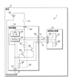
- FIG. 2 is a block diagram showing a configuration of main parts of an in-vehicle system according to Embodiment 1;
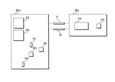
- FIG. It is a top view of an electric equipment and a switch apparatus. 4 is a timing chart for explaining the operation of the switching circuit;
- FIG. 11 is a block diagram showing the main configuration of an in-vehicle system according to Embodiment 2;
- the present disclosure has been made in view of such circumstances, and its object is to provide an electrical device capable of preventing the inflow of overcurrent through a conductor, and an in-vehicle system including the electrical device. That's what it is.
- the electronic component is, for example, a microcomputer, and outputs or detects a voltage based on the potential of the first connecting portion.
- the second switch when the voltage between the first connection portion and the second connection portion exceeds the predetermined voltage, the second switch is turned on. This causes the voltage across the output and control ends of the switch to drop to 0V, which is below the threshold. As a result, the switch turns off.
- An in-vehicle system is an in-vehicle system in which an electrical device outputs voltage to a second electrical device, or the second electrical device outputs voltage to the electrical device.
- the electric device includes a first connection portion connected to a vehicle body, a second connection portion connected to the second electric device, and a connection portion connected between the first connection portion and the second connection portion. and a switching circuit for switching the switch on or off, wherein when the switch is on, current flows in the order of the second connection, the switch and the first connection, the switching circuit comprising: and switching the switch from ON to OFF when the voltage between the first connection and the second connection exceeds a predetermined voltage.
- the substrate is connected to the second substrate by the conductor. For this reason, there is a high possibility that a power short-circuit of the conducting wire will occur. As a result, there is a high demand for a function that prevents overcurrent from flowing through the conductors in electrical equipment.
- the electric device 10 has a power terminal 30 , a ground terminal 31 and a device connector 32 .
- the switch device 11 has an input terminal 40 , an output terminal 41 , a device connector 42 , a power supply switch 43 and a drive circuit 44 .
- the power supply switch 43 is an N-channel FET (Field Effect Transistor). When the power supply switch 43 is on, the resistance between the drain and source is sufficiently small. This allows current to flow through the drain and source. When the power supply switch 43 is off, the resistance between the drain and source is sufficiently large. Therefore, no current flows through the drain and source.
- the drive circuit 44 switches the power supply switch 43 on or off.
- the negative electrode of the DC power supply 20 is connected to the body E of the vehicle C.
- Body E is a conductor.
- a connection to the body E provides grounding.
- a positive electrode of the DC power supply 20 is connected to one end of the power switch 21 .
- the other end of the power switch 21 is detachably connected to the power terminal 30 of the electric device 10 and detachably connected to the input terminal 40 of the switch device 11 .
- a ground terminal 31 of the electrical device 10 is connected to the body E. As shown in FIG.
- the ground terminal 31 functions as a first connection portion.
- One end of the load 22 is detachably connected to the output terminal 41 of the switch device 11 .
- the other end of the load 22 is connected to the body E.
- the device connector 32 of the electrical device 10 is detachably connected to one ends of the signal line F and the ground line G. As shown in FIG. The other ends of the signal line F and the ground line G are detachably connected to the device connector 42 of the switch device 11 . The signal line F and the ground line G are conducting lines.
- the device connector 32 is connected to the device connector 42 by a signal line F and a ground line G.
- FIG. The switch device 11 functions as an external device and a second electrical device.
- the device connector 32 functions as a second connection.
- the drain and source of the power supply switch 43 are connected to the input terminal 40 and the output terminal 41, respectively.
- the power switch 21 When the power switch 21 is on, current flows from the positive electrode of the DC power supply 20 to the power switch 21 , the electrical equipment 10 , the body E, and the negative electrode of the DC power supply 20 in this order. Thereby, electric power is supplied to the electric device 10 .
- the electric device 10 operates while the electric power is supplied to the electric device 10 .
- the electric device 10 instructs the drive circuit 44 of the switch device 11 to switch the power supply switch 43 on or off.
- the power switch 21 and the power supply switch 43 When the power switch 21 and the power supply switch 43 are on, the current flows from the positive terminal of the DC power supply 20 to the power switch 21, the input terminal 40, the power supply switch 43, the output terminal 41, the load 22, the body E and the negative terminal of the DC power supply 20. flow in the order of Thereby, power is supplied to the load 22 .
- the power switch 21 or the power supply switch 43 When the power switch 21 or the power supply switch 43 is off, current flow through the power supply switch 43 is stopped. Therefore, power supply from the DC power supply 20 to the load 22 is stopped.
- the load 22 is, for example, a lamp.
- the load 22 operates while the DC power supply 20 is supplying power to the load 22 .
- the load 22 stops operating.
- the electrical equipment 10 and the switch device 11 control power supply from the DC power supply 20 to the load 22 .
- the power switch 21 is off, power supply from the DC power supply 20 to the electrical equipment 10 stops. In this case, the electrical device 10 has stopped operating.
- the electrical equipment 10 has a switching circuit 33 , a regulator 34 , a microcomputer (hereinafter referred to as a microcomputer) 35 , and a connection switch 36 in addition to a power terminal 30 , a ground terminal 31 and a device connector 32 .
- the switching circuit 33 has a circuit switch 50 , a first circuit resistor 51 and a second circuit resistor 52 .
- the connection switch 36 and the circuit switch 50 are NPN type bipolar transistors.
- the power supply terminal 30 is connected to one end of the first circuit resistor 51 of the switching circuit 33 and the regulator 34 .
- the other end of the first circuit resistor 51 is connected to the collector of the circuit switch 50 .
- Circuit switch 50 functions as a second switch.
- the base of circuit switch 50 is connected to one end of second circuit resistor 52 .
- a connection node between the collector of the circuit switch 50 and the first circuit resistor 51 is connected to the base of the connection switch 36 .
- the emitter and collector of the connection switch 36 are connected to the ground terminal 31 and the device connector 32, respectively.
- the emitter of circuit switch 50 is connected to the connection node between the emitter of connection switch 36 and ground terminal 31 .
- the other end of the second circuit resistor 52 is connected to the ground terminal 31 .
- the regulator 34 is further connected to the ground terminal 31 and the microcomputer 35.
- the microcomputer 35 is also connected to the ground terminal 31 and the equipment connector 32 .
- a connection node between the instrument connector 32 and the collector of the connection switch 36 is connected to a connection node between the base of the circuit switch 50 and the second circuit resistor 52 .
- the gate of the power supply switch 43 is connected to the drive circuit 44 .
- the drive circuit 44 is further connected to the connection node between the input terminal 40 and the power supply switch 43 and the device connector 42 .
- the regulator 34 and the first circuit resistor 51 are connected to the power switch 21 via the power terminal 30 .
- the regulator 34 , the microcomputer 35 , the emitter of the connection switch 36 , the emitter of the circuit switch 50 and the other end of the second circuit resistor 52 are connected to the body E via the ground terminal 31 .
- the microcomputer 35 is connected to the signal line F via the equipment connector 32 .
- the collector of the connection switch 36 , the base of the circuit switch 50 , and one end of the second circuit resistor 52 are each connected to the ground line G via the device connector 32 .
- the drive circuit 44 is separately connected to the signal line F and the ground line G via the device connector 42 .
- the drain of the power supply switch 43 and the drive circuit 44 are each connected to the power switch 21 via the input terminal 40 .
- a source of the power supply switch 43 is connected to the load 22 via the output terminal 41 .
- FIG. 2 is a plan view of the electrical equipment 10 and the switch device 11.
- Each of the electrical device 10 and the switch device 11 has a device substrate Bm and a device substrate Bs.
- Each of the device substrate Bm and the device substrate Bs has a rectangular plate shape.
- a regulator 34, a microcomputer 35, a connection switch 36, a circuit switch 50, a first circuit resistor 51 and a second circuit resistor 52 are arranged on the wide surface of the device substrate Bm.
- Each of the regulator 34 and the microcomputer 35 is, for example, an integrated circuit element. With respect to a plate, the wide face is a different face than the end faces.
- a power supply switch 43 and a drive circuit 44 are arranged on the wide surface of the device substrate Bs.
- the drive circuit 44 is, for example, an integrated circuit element.
- the equipment board Bm and the device board Bs are connected by a signal line F.
- the equipment board Bm and the device board Bs are further connected by a ground line G.
- FIG. 2 illustration of the power supply terminal 30, the ground terminal 31, the device connector 32, the input terminal 40, the output terminal 41, and the device connector 42 is omitted.
- the power terminal 30, the ground terminal 31, and the device connector 32 are arranged on the wide surface of the device board Bm.
- the input terminal 40, the output terminal 41 and the device connector 42 are arranged on the wide surface of the device board Bs.
- the device substrate Bs functions as a second substrate.
- the voltage of the positive electrode of the DC power supply 20 with the potential of the negative electrode is referred to as the power supply voltage. Since the ground terminal 31 is connected to the body E, the power supply voltage is a positive voltage with the potential of the ground terminal 31 as a reference potential.
- the power switch 21 When the power switch 21 is on, current flows from the positive terminal of the DC power supply 20 to the power switch 21, the power terminal 30, the regulator 34, the ground terminal 31, the body E, and the negative terminal of the DC power supply 20 in this order.
- the power supply voltage of the DC power supply 20 is applied to the regulator 34 and power is supplied to the regulator 34 .
- Regulator 34 operates while power is being supplied.
- the regulator 34 steps down the power supply voltage to a constant target voltage.
- the regulator 34 applies the target voltage obtained by stepping down to the microcomputer 35 .
- the target voltage is a voltage with the potential of the ground terminal 31 as a reference potential.
- the power supply voltage is, for example, 12V.
- the target voltage is 3.3V, 5.5V, or the like.
- the regulator 34 applies the target voltage to the microcomputer 35, the current flows from the positive terminal of the DC power supply 20 to the power switch 21, the power terminal 30, the regulator 34, the microcomputer 35, the ground terminal 31, the body E, and the DC power supply 20. Electricity is supplied to the microcomputer 35 by flowing in the order of the negative electrode.
- the microcomputer 35 operates while power is being supplied.
- the drive circuit 44 While the power supplied to the drive circuit 44 of the switch device 11 is less than the predetermined power, the drive circuit 44 stops operating. The drive circuit 44 operates while the power supplied to the drive circuit 44 is equal to or higher than the predetermined power.
- connection switch 36 and the circuit switch 50 For each of the connection switch 36 and the circuit switch 50, the resistance between the collector and emitter is sufficiently small when the state is ON. Therefore, current can flow in the order collector and emitter. For each connection switch 36 and circuit switch 50, the resistance between the collector and emitter is sufficiently high when the state is off. Therefore, no current flows through the collector and emitter.
- the switching circuit 33 switches the connection switch 36 on or off according to the voltage of the ground line G with the potential of the ground terminal 31 as a reference potential.
- the connection switch 36 When the power switch 21 is on and the connection switch 36 is on, the current flows from the positive pole of the DC power supply 20 to the power switch 21, the input terminal 40, the drive circuit 44, the device connector 42, the ground line G, the equipment. It flows through the connector 32 , the connection switch 36 , the ground terminal 31 , the body E, and the negative electrode of the DC power supply 20 in that order. Due to this current flow, the drive circuit 44 is supplied with power equal to or greater than the predetermined power.
- the connection switch 36 When the connection switch 36 is on, the current flows in the order of the collector and the emitter in the connection switch 36 . Therefore, the collector of the connection switch 36 functions as an input terminal to which current is input. The emitter of the connection switch 36 functions as an output terminal through which current is output.
- the current flows from the positive terminal of the DC power supply 20 to the power switch 21, the input terminal 40, the drive circuit 44, the device connector 42, the ground line G, the equipment.
- the current flows through the connector 32 , the second circuit resistor 52 , the ground terminal 31 , the body E, and the negative electrode of the DC power supply 20 in this order. Since the current flows through the second circuit resistor 52, the power supplied to the drive circuit 44 is small. As a result, the power supplied to the drive circuit 44 is less than the predetermined power due to the current flowing through the drive circuit 44 and the second circuit resistor 52 .
- the state of the power supply switch 43 when the voltage of the gate with the potential of the source as the reference potential is equal to or higher than a certain voltage, the state is ON. When the voltage of the gate with the potential of the source as the reference potential is less than the constant voltage, the state of the power supply switch 43 is off.
- the microcomputer 35 of the electric device 10 outputs a high level voltage or a low level voltage to the drive circuit 44 of the switch device 11 via the signal line F.
- the output voltage of the microcomputer 35 is a voltage with the potential of the ground terminal 31 as a reference potential.
- the microcomputer 35 functions as an electronic component.
- the microcomputer 35 switches the output voltage to be output to the drive circuit 44 via the signal line F to a low level voltage or a high level voltage.
- the drive circuit 44 detects the voltage of the signal line F using the potential of the ground line G as a reference potential. When the connection switch 36 is on, the potential of the ground line G substantially matches the potential of the ground terminal 31, that is, the ground potential. Therefore, the voltage of the signal line F detected by the drive circuit 44 is the output voltage of the microcomputer 35 .
- the drive circuit 44 switches the gate of the power supply switch 43 to the ground line G potential as the reference potential. Increase voltage. As a result, in the power supply switch 43, the voltage of the gate with the potential of the source as the reference potential rises to a value equal to or higher than a certain voltage, and the power supply switch 43 is turned on.
- the drive circuit 44 lowers the voltage of the gate of the power supply switch 43 with the potential of the ground line G as the reference potential.
- the voltage of the gate with the potential of the source as the reference potential drops to a value less than the constant voltage, and the power supply switch 43 is switched off.
- connection switch 36 When the switching circuit 33 switches the connection switch 36 from ON to OFF, current flow through the ground line G, the connection switch 36 and the ground terminal 31 stops.
- connection switch 36 is ON when the base voltage with the emitter potential as the reference potential is equal to or higher than a certain threshold.
- the threshold is positive. If the voltage at the base referenced to the potential at the emitter is less than the threshold, the state is off. Therefore, the connection switch 36 is switched from ON to OFF when the voltage of the base with the potential of the emitter as the reference potential drops to a value less than the threshold.
- the base of connection switch 36 functions as a control end.
- the state is ON when the base voltage with the emitter potential as the reference potential is equal to or higher than a certain reference voltage. If the voltage at the base, referenced to the potential at the emitter, is less than the reference voltage, the state is off.
- the reference voltage is positive.
- the emitter of circuit switch 50 is connected to ground terminal 31 .
- the base of the circuit switch 50 is connected to the ground line G. Therefore, regarding the circuit switch 50, the voltage of the base with the potential of the emitter as the reference potential is the voltage of the ground line G with the potential of the ground terminal 31 as the reference potential.
- the circuit switch 50 is switched from OFF to ON when the voltage of the ground line G with the potential of the ground terminal 31 as a reference potential rises to a value equal to or higher than the reference voltage.
- the voltage of the ground line G matches the voltage of the portion of the device connector 32 that is connected to the ground line G. FIG. Therefore, the voltage on the ground line G corresponds to the voltage on the device connector 32 .
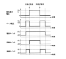
- FIG. 3 is a timing chart for explaining the operation of the switching circuit 33.
- the voltage of the base with the potential of the ground terminal 31 as the reference potential is referred to as the base voltage.
- FIG. 3 shows transitions of the base voltage and the ground line G voltage.
- the reference potential of the voltage of the ground line G is the potential of the ground terminal 31, that is, the potential of the body E.
- the voltage on the ground line G corresponds to the voltage on the equipment connector 32 .
- FIG. 3 shows transitions of states of the power switch 21, the circuit switch 50, and the connection switch 36.
- Vb is the power supply voltage of the DC power supply 20 .
- Vth and Vr are the threshold and reference voltages, respectively.
- the power supply voltage is a positive voltage with the potential of the ground terminal 31 as a reference potential.
- the ground line G is arranged between the equipment board Bm and the device board Bs. Therefore, the ground wire G may come into contact with the conductor connected to the positive electrode of the DC power supply 20 . If the ground wire G contacts the conducting wire, the ground wire G may be connected to the positive electrode of the DC power supply 20 . A phenomenon in which the ground line G is connected to the positive terminal of the DC power supply 20 is called power fault. When a power short-circuit occurs in the ground line G, the voltage of the ground line G rises to the power supply voltage Vb.
- the circuit switch 50 When the circuit switch 50 is off, little current flows through the first circuit resistor 51 . Therefore, when the power switch 21 is switched from off to on, the base voltage of the connection switch 36 rises to the power supply voltage Vb. Since the threshold Vth is equal to or lower than the power supply voltage Vb, the connection switch 36 is switched from off to on when the base voltage of the connection switch 36 rises to the power supply voltage Vb. As described above, when the connection switch 36 is on, the potential of the ground line G substantially matches the potential of the ground terminal 31, that is, the ground potential.
- the circuit switch 50 When a short-circuit occurs in the ground line G, the voltage of the ground line G rises to the power supply voltage Vb. Since the power supply voltage Vb is equal to or higher than the reference voltage Vr, the circuit switch 50 is switched from off to on when the voltage of the ground line G rises to the power supply voltage Vb. When the circuit switch 50 turns on, the base voltage of the connection switch 36 drops to 0V, which is below the threshold Vth. As a result, the connection switch 36 is switched from on to off.
- connection switch 36 When the connection switch 36 is off, no current flows through the ground line G and the connection switch 36. Current flows through the ground line G, the device connector 32 , the second circuit resistor 52 and the ground terminal 31 in this order. Since the current flows through the second circuit resistance 52, the current flowing into the electric device 10 through the ground line G is small. Inflow of overcurrent to the electrical equipment 10 via the ground line G is prevented.
- the resistance of the second circuit resistor 52 is sufficiently greater than the collector-to-emitter resistance of the connection switch 36 that is on.
- connection switch 36 is kept off while the voltage of the ground line G is equal to or higher than the reference voltage Vr.
- the power supply switch 21 When the power supply switch 21 is turned on and the grounding wire G is disconnected, the current flows from the positive electrode of the DC power supply 20 to the power switch 21, the input terminal 40, the drive circuit 44, the device connector 42, and the grounding wire G. , the device connector 32 , the second circuit resistor 52 , the ground terminal 31 , the body E, and the negative electrode of the DC power supply 20 . As a result, the voltage of the ground line G drops below the reference voltage Vr. As a result, the circuit switch 50 switches from ON to OFF.
- the connection switch 36 When the circuit switch 50 is switched off, the base voltage of the connection switch 36 rises to the power supply voltage Vb, and the connection switch 36 is switched from off to on.
- the connection switch 36 When the connection switch 36 is turned on, the voltage of the ground line G drops to 0V.
- the resistance value of the second circuit resistor 52 is from the positive electrode of the DC power supply 20, and the current is from the power switch 21, the input terminal 40, the drive circuit 44, the device connector 42, the ground line G, the device connector 32, the second circuit resistor 52, This is the value at which the voltage of the ground line G drops to a voltage less than the reference voltage Vr when the current flows in the order of the ground terminal 31, the body E, and the negative electrode of the DC power supply 20.
- the switching circuit 33 switches the connection switch 36 from ON to OFF when the voltage of the ground line G with the potential of the ground terminal 31 as a reference potential rises to a value equal to or higher than the reference voltage. Therefore, when the ground line G is short-circuited to the power supply, the connection switch 36 is switched from ON to OFF, and overcurrent is prevented from flowing into the electric device 10 via the ground line G. Since the device board Bm is connected to the device board Bs of the switch device 11 by the ground line G, there is a high possibility that the ground line G will be short-circuited. Therefore, there is a high need for a function to prevent overcurrent from flowing through the ground line G.
- the switching performed by the switching circuit 33 does not use a processing element that executes processing according to a program.
- the switching circuit 33 is configured by hardware. Therefore, the period from when the voltage of the ground line G with the potential of the ground terminal 31 as a reference potential rises to a value equal to or higher than the reference voltage until the connection switch 36 is switched from on to off is short.
- the load 22 is arranged outside the switch device 11 .
- the place where the load 22 is arranged is not limited to the outside of the switch device 11 .
- switch device 11 may have load 22 .
- the load 22 is arranged, for example, on the wide surface of the device board Bs of the switch device 11 .
- the power supply switch 43 of the switch device 11 is a switch that can be switched by the drive circuit 44 . Therefore, the power supply switch 43 is not limited to an N-channel FET, and may be a P-channel FET, a bipolar transistor, a relay contact, or the like. Also, if the device connected to the electric device 10 is a device that operates according to the output voltage of the microcomputer 35, there is no problem. Therefore, the device connected to the electrical device 10 is not limited to the switch device 11. FIG.
- Embodiment 2 The electric device 10 according to the first embodiment outputs voltage to the switch device 11 via the signal line F.
- FIG. the operation performed by the electrical device 10 is not limited to voltage output.
- the points of the second embodiment that are different from the first embodiment will be described. Configurations other than those described later are common to those of the first embodiment. For this reason, the same reference numerals as in Embodiment 1 are given to the components that are common to Embodiment 1, and the description of those components is omitted.
- FIG. 4 is a block diagram showing the main configuration of the in-vehicle system 1 according to the second embodiment.
- the in-vehicle system 1 according to the second embodiment has a temperature detection device 12 instead of the switch device 11 .
- the temperature detection device 12 is mounted on the vehicle C. As shown in FIG. Temperature sensing device 12 has a second device connector 60 . In Embodiment 2, the temperature detection device 12 functions as an external device and a second electrical device.
- the device connector 32 of the electrical device 10 is detachably connected to one ends of the signal line F and the ground line G.
- the device connector 32 is also detachably connected to one end of the voltage line H.
- the other ends of the voltage line H, the signal line F and the ground line G are detachably connected to the second device connector 60 of the temperature detection device 12 .
- the voltage line H is a conducting wire.
- the temperature detection device 12 detects the temperature inside the vehicle C, the temperature of the semiconductor switch, or the like.
- the temperature detection device 12 outputs a voltage indicating the detected temperature to the electrical equipment 10 .
- connection node between the power terminal 30 and the first circuit resistor 51 of the switching circuit 33 is connected to the device connector 32 .
- This connection node is connected to the voltage line H via the equipment connector 32 .
- the temperature detection device 12 has a fixed resistor 61 and a thermistor 62 in addition to the second device connector 60 .
- the resistance value of the fixed resistor 61 is constant regardless of the temperature of the fixed resistor 61 .
- the resistance value of the thermistor 62 varies according to the temperature of the thermistor 62 .
- the thermistor 62 is of the NTC (Negative Temperature Coefficient) type
- the thermistor 62 is of the PTC (Positive Temperature Coefficient) type
- the environmental temperature around the thermistor 62 can be detected using the thermistor 62 . Therefore, when detecting the temperature in the interior of the vehicle C, the thermistor 62 is arranged in the interior of the vehicle C. As shown in FIG. When detecting the temperature of the semiconductor switch, it is arranged near the semiconductor switch.
- One end of the fixed resistor 61 is connected to the second device connector 60 .
- the other end of the fixed resistor 61 is connected to one end of the thermistor 62 .
- the other end of the thermistor 62 is connected to the second device connector 60 .
- a connection node between the fixed resistor 61 and the thermistor 62 is connected to the second device connector 60 .
- One end of the fixed resistor 61 is connected to the voltage line H via the second device connector 60 .
- a connection node between the fixed resistor 61 and the thermistor 62 is connected to the signal line F via the second device connector 60 .
- the other end of thermistor 62 is connected to ground line G via second device connector 60 .
- the temperature detection device 12 may have a device substrate Bs, like the switch device 11 of the first embodiment.
- a second device connector 60, a fixed resistor 61 and a thermistor 62 are arranged on the wide surface of the device substrate Bs.
- the switching circuit 33 keeps the connection switch 36 on when the ground line G is not short-circuited to power.
- the current flows from the positive electrode of the DC power supply 20 to the power switch 21, the power terminal 30, the device connector 32, the voltage line H, the second device connector 60, the fixed resistor 61, The thermistor 62 , the second device connector 60 , the ground line G, the device connector 32 , the circuit switch 50 , the ground terminal 31 , the body E, and the negative electrode of the DC power supply 20 flow in this order.
- the power supply voltage of the DC power supply 20 is applied between one end of the fixed resistor 61 and the other end of the thermistor 62 via the voltage line H and the ground line G.
- the fixed resistor 61 and the thermistor 62 divide the power supply voltage.
- a divided voltage obtained by dividing the voltage is output from the temperature detection device 12 to the microcomputer 35 of the electric device 10 via the signal line F.
- FIG. The divided voltage is a voltage using the potential of the ground line G as a reference potential.
- the microcomputer 35 outputs a high level voltage or a low level voltage via the signal line F.
- the microcomputer 35 detects the voltage of the signal line F using the potential of the ground terminal 31 as a reference potential instead of outputting the voltage.
- the connection switch 36 is on, the voltage detected by the microcomputer 35 substantially matches the divided voltage.
- the resistance value of the second circuit resistor 52 is adjusted so that the voltage of the ground line G with the potential of the ground terminal 31 as a reference potential drops below the reference voltage Vr. Therefore, the resistance value of the second circuit resistor 52 is less than the minimum combined resistance value of the fixed resistor 61 and the thermistor 62 .
- Embodiment 2 the locations where the fixed resistor 61 and the thermistor 62 are connected may be exchanged. In this case, one end of the fixed resistor 61 is connected to the ground line G. FIG. The other end of the thermistor 62 is connected to the voltage line H. When the locations where the fixed resistor 61 and the thermistor 62 are connected are switched, the divided voltage is lower as the resistance value of the thermistor 62 is larger.
- the voltage applied to the circuit including the fixed resistor 61 and the thermistor 62 is not limited to the power supply voltage, and may be the target voltage generated by the regulator 34, for example.
- the connection node between the regulator 34 and the microcomputer 35 is connected to the voltage line H through the device connector 32 instead of the connection node between the power supply terminal 30 and the first circuit resistor 51 .
- a fixed resistor 61 and a thermistor 62 divide the target voltage.
- connection switch 36 is not limited to an NPN-type bipolar transistor, and may be an N-channel FET, an IGBT (Insulated Gate Bipolar Transistor), or the like.
- circuit switch 50 is not limited to an NPN-type bipolar transistor, and may be an N-channel FET, IGBT, or the like.
- the power terminal 30 of the electrical device 10 may be directly connected to the positive electrode of the DC power supply 20 .
Landscapes
- Engineering & Computer Science (AREA)
- Mechanical Engineering (AREA)
- Emergency Protection Circuit Devices (AREA)
- Direct Current Feeding And Distribution (AREA)
Abstract
Description
本出願は、2022年1月12日出願の日本出願第2022-003272号に基づく優先権を主張し、前記日本出願に記載された全ての記載内容を援用するものである。
特許文献1に関して、グランド線に車両のバッテリの正極が接続される天絡が発生した場合、グランド線から電気機器に過電流が流れ込む可能性がある。過電流が電気機器内を流れた場合、電気機器内の部品が故障する可能性がある。
上記の態様によれば、導線を介した過電流の流入を防止することができる。
最初に本開示の実施態様を列挙して説明する。以下に記載する実施形態の少なくとも一部を任意に組み合わせてもよい。
本開示の実施形態に係る車載システムの具体例を、以下に図面を参照しつつ説明する。なお、本開示はこれらの例示に限定されるものではなく、請求の範囲によって示され、請求の範囲と均等の意味および範囲内でのすべての変更が含まれることが意図される。
図1は、実施形態1における車載システム1の要部構成を示すブロック図である。車載システム1は、車両Cに搭載されている。車両Cには、更に、直流電源20、電源スイッチ21及び負荷22が搭載されている。車載システム1は、電気機器10及びスイッチ装置11を有する。直流電源20は、例えばバッテリである。電源スイッチ21は、例えば、イグニッション電源又はアクセサリー電源がオンに切替わった場合にオンに切替わる。この構成では、電源スイッチ21は、イグニッション電源又はアクセサリー電源がオフに切替わった場合にオフに切替わる。
電気機器10は、電源端子30、接地端子31及び機器コネクタ32に加えて、切替え回路33、レギュレータ34及びマイクロコンピュータ(以下、マイコンという)35、及び接続スイッチ36を有する。切替え回路33は、回路スイッチ50、第1回路抵抗51及び第2回路抵抗52を有する。接続スイッチ36及び回路スイッチ50は、NPN型のバイポーラトランジスタである。
前述したように、切替え回路33は、接地端子31の電位を基準電位とした接地線Gの電圧が基準電圧以上の値に上昇した場合、接続スイッチ36をオンからオフに切替える。従って、接地線Gの天絡が発生した場合、接続スイッチ36がオンからオフに切替わり、接地線Gを介した電気機器10への過電流の流入が防止される。機器基板Bmが接地線Gによってスイッチ装置11の装置基板Bsに接続されているので、接地線Gの天絡が発生する可能性が高い。このため、接地線Gを介した過電流の流入を防止する機能の必要性が高い。
実施形態1では、負荷22はスイッチ装置11の外側に配置されている。しかしながら、負荷22が配置される場所は、スイッチ装置11の外側に限定されない。例えば、スイッチ装置11が負荷22を有してもよい。この場合、負荷22は、例えば、スイッチ装置11の装置基板Bsの幅広面に配置される。
実施形態1における電気機器10は、信号線Fを介して電圧をスイッチ装置11に出力している。しかしながら、電気機器10が行う動作は電圧の出力に限定されない。
以下では、実施形態2について、実施形態1と異なる点を説明する。後述する構成を除く他の構成については、実施形態1と共通している。このため、実施形態1と共通する構成部には実施形態1と同一の参照符号を付し、その構成部の説明を省略する。
図4は、実施形態2における車載システム1の要部構成を示すブロック図である。実施形態2を実施形態1と比較した場合、電気機器10に接続される装置が異なる。実施形態2における車載システム1は、スイッチ装置11の代わりに温度検出装置12を有する。温度検出装置12は車両Cに搭載されている。温度検出装置12は、第2の装置コネクタ60を有する。実施形態2では、温度検出装置12が外部機器及び第2の電気機器として機能する。
電気機器10では、電源端子30と、切替え回路33の第1回路抵抗51との間の接続ノードは機器コネクタ32に接続されている。この接続ノードは、機器コネクタ32を介して電圧線Hに接続される。
実施形態2における電気機器10は、実施形態1における電気機器10が奏する効果を同様に奏する。
実施形態2では、固定抵抗61及びサーミスタ62が接続される場所を入れ替えてもよい。この場合、固定抵抗61の一端は接地線Gに接続される。サーミスタ62の他端は電圧線Hに接続される。固定抵抗61及びサーミスタ62が接続される場所が入れ替わった場合、分圧電圧は、サーミスタ62の抵抗値が大きい程、低い。
実施形態1,2では、接続スイッチ36は、NPN型のバイポーラトランジスタに限定されず、Nチャネル型のFET又はIGBT(Insulated Gate Bipolar Transistor)等であってもよい。同様に、回路スイッチ50は、NPN型のバイポーラトランジスタに限定されず、Nチャネル型のFET又はIGBT等であってもよい。電気機器10の電源端子30は、直流電源20の正極に直接に接続されてもよい。
開示された実施の形態1,2はすべての点で例示であって、制限的なものではないと考えられるべきである。本発明の範囲は、上記した意味ではなく、請求の範囲によって示され、請求の範囲と均等の意味及び範囲内でのすべての変更が含まれることが意図される。
10 電気機器
11 スイッチ装置(外部機器、第2の電気機器)
12 温度検出装置(外部機器、第2の電気機器)
20 直流電源
21 電源スイッチ
22 負荷
30 電源端子
31 接地端子(第1接続部)
32 機器コネクタ(第2接続部)
33 切替え回路
34 レギュレータ
35 マイコン(電子部品)
36 接続スイッチ
40 入力端子
41 出力端子
42 装置コネクタ
43 給電スイッチ
44 駆動回路
50 回路スイッチ(第2のスイッチ)
51 第1回路抵抗
52 第2回路抵抗
60 第2の装置コネクタ
61 固定抵抗
62 サーミスタ
Bm 機器基板
Bs 装置基板(第2の基板)
C 車両
E ボデー
F 信号線
G 接地線
H 電圧線
Claims (6)
- 車両に搭載される電気機器であって、
前記車両のボデーに接続される第1接続部と、
外部機器に接続される第2接続部と、
前記第1接続部及び第2接続部間に接続されるスイッチと、
前記スイッチをオン又はオフに切替える切替え回路と
を備え、
前記スイッチがオンである場合、電流は、前記第2接続部、スイッチ及び第1接続部の順に流れ、
前記切替え回路は、前記第1接続部及び第2接続部間の電圧が所定電圧以上となった場合、前記スイッチをオンからオフに切替える
電気機器。 - 前記第1接続部の電位を基準電位とした電圧の出力又は検出を行う電子部品
を備える請求項1に記載の電気機器。 - 前記スイッチ及び切替え回路が配置される基板を備え、
前記基板は前記外部機器と接続される
請求項1又は請求項2に記載の電気機器。 - 前記スイッチは、電流が出力される出力端と制御端との間の電圧が閾値未満となった場合にオンからオフに切替わり、
前記切替え回路は、前記スイッチの出力端及び制御端間に接続される第2のスイッチを有し、
前記第2のスイッチは、前記第1接続部及び第2接続部間の電圧が前記所定電圧以上となった場合にオフからオンに切替わる
請求項1から請求項3のいずれか1項に記載の電気機器。 - 電気機器が第2の電気機器に電圧を出力するか、又は、前記第2の電気機器が前記電気機器に電圧を出力する車載システムであって、
前記電気機器は、
車両のボデーに接続される第1接続部と、
前記第2の電気機器に接続される第2接続部と、
前記第1接続部及び第2接続部間に接続されるスイッチと、
前記スイッチをオン又はオフに切替える切替え回路と
を有し、
前記スイッチがオンである場合、電流は、前記第2接続部、スイッチ及び第1接続部の順に流れ、
前記切替え回路は、前記第1接続部及び第2接続部間の電圧が所定電圧以上となった場合、前記スイッチをオンからオフに切替える
車載システム。 - 前記電気機器は、前記スイッチ及び切替え回路が配置される基板を有し、
前記第2の電気機器は第2の基板を有し、
前記基板は前記第2の基板に接続される
請求項5に記載の車載システム。
Priority Applications (2)
| Application Number | Priority Date | Filing Date | Title |
|---|---|---|---|
| US18/727,517 US20250174977A1 (en) | 2022-01-12 | 2022-12-27 | Electrical equipment and in-vehicle system |
| CN202280085834.XA CN118414268A (zh) | 2022-01-12 | 2022-12-27 | 电气设备及车载系统 |
Applications Claiming Priority (2)
| Application Number | Priority Date | Filing Date | Title |
|---|---|---|---|
| JP2022-003272 | 2022-01-12 | ||
| JP2022003272A JP7666339B2 (ja) | 2022-01-12 | 2022-01-12 | 電気機器及び車載システム |
Publications (1)
| Publication Number | Publication Date |
|---|---|
| WO2023136128A1 true WO2023136128A1 (ja) | 2023-07-20 |
Family
ID=87279077
Family Applications (1)
| Application Number | Title | Priority Date | Filing Date |
|---|---|---|---|
| PCT/JP2022/048078 Ceased WO2023136128A1 (ja) | 2022-01-12 | 2022-12-27 | 電気機器及び車載システム |
Country Status (4)
| Country | Link |
|---|---|
| US (1) | US20250174977A1 (ja) |
| JP (1) | JP7666339B2 (ja) |
| CN (1) | CN118414268A (ja) |
| WO (1) | WO2023136128A1 (ja) |
Citations (2)
| Publication number | Priority date | Publication date | Assignee | Title |
|---|---|---|---|---|
| JP2017060032A (ja) * | 2015-09-17 | 2017-03-23 | 新日本無線株式会社 | 出力回路 |
| JP2018013401A (ja) * | 2016-07-20 | 2018-01-25 | 株式会社デンソーテン | 空燃比センサの制御装置および異常検出方法 |
Family Cites Families (2)
| Publication number | Priority date | Publication date | Assignee | Title |
|---|---|---|---|---|
| JP3314922B2 (ja) * | 1999-06-21 | 2002-08-19 | ナルデック株式会社 | 負荷駆動システム及びその故障検出方法 |
| JP4149778B2 (ja) * | 2002-10-28 | 2008-09-17 | 矢崎総業株式会社 | 車両用電力制御装置 |
-
2022
- 2022-01-12 JP JP2022003272A patent/JP7666339B2/ja active Active
- 2022-12-27 CN CN202280085834.XA patent/CN118414268A/zh active Pending
- 2022-12-27 US US18/727,517 patent/US20250174977A1/en active Pending
- 2022-12-27 WO PCT/JP2022/048078 patent/WO2023136128A1/ja not_active Ceased
Patent Citations (2)
| Publication number | Priority date | Publication date | Assignee | Title |
|---|---|---|---|---|
| JP2017060032A (ja) * | 2015-09-17 | 2017-03-23 | 新日本無線株式会社 | 出力回路 |
| JP2018013401A (ja) * | 2016-07-20 | 2018-01-25 | 株式会社デンソーテン | 空燃比センサの制御装置および異常検出方法 |
Also Published As
| Publication number | Publication date |
|---|---|
| US20250174977A1 (en) | 2025-05-29 |
| CN118414268A (zh) | 2024-07-30 |
| JP7666339B2 (ja) | 2025-04-22 |
| JP2023102646A (ja) | 2023-07-25 |
Similar Documents
| Publication | Publication Date | Title |
|---|---|---|
| US11038371B2 (en) | Power supply control device | |
| CN109477862B (zh) | 车载控制装置 | |
| CN109314386B (zh) | 供电控制装置 | |
| US10135234B2 (en) | Preventive apparatus | |
| KR100355685B1 (ko) | 전력반도체스위치및자동전기시스템 | |
| CN111033288B (zh) | 异常检测装置 | |
| WO2023136128A1 (ja) | 電気機器及び車載システム | |
| US10921384B2 (en) | Disconnection sensing circuit and electrical connection box | |
| JP2003308123A (ja) | 電源保護回路 | |
| JP2019198171A (ja) | 電力供給装置 | |
| JP7697348B2 (ja) | 制御装置 | |
| US12587003B2 (en) | On-board device | |
| CN113785255A (zh) | 电压调节器以及车载用的备用电源 | |
| US10599198B2 (en) | Load driving device | |
| JP7310591B2 (ja) | 駆動装置 | |
| US20250233404A1 (en) | Switch device, electronic device and vehicle | |
| US7906946B2 (en) | Semiconductor integrated circuit device for providing series regulator | |
| US20250309884A1 (en) | Switch device, load drive system, and switch system | |
| US12181946B2 (en) | Abnormality detection circuit, semiconductor device, electronic apparatus, and vehicle | |
| US20240170956A1 (en) | Signal output circuit and semiconductor integrated circuit device | |
| JP2025148149A (ja) | サージ保護回路 | |
| JP2020137352A (ja) | 電力供給装置 | |
| JP4327611B2 (ja) | 短絡用回路およびエンジンのアンチノック制御装置 | |
| JPH04326108A (ja) | 負荷駆動制御装置 | |
| JP2002312040A (ja) | 負荷制御装置 |
Legal Events
| Date | Code | Title | Description |
|---|---|---|---|
| 121 | Ep: the epo has been informed by wipo that ep was designated in this application |
Ref document number: 22919291 Country of ref document: EP Kind code of ref document: A1 |
|
| WWE | Wipo information: entry into national phase |
Ref document number: 202280085834.X Country of ref document: CN |
|
| WWE | Wipo information: entry into national phase |
Ref document number: 18727517 Country of ref document: US |
|
| NENP | Non-entry into the national phase |
Ref country code: DE |
|
| 122 | Ep: pct application non-entry in european phase |
Ref document number: 22919291 Country of ref document: EP Kind code of ref document: A1 |
|
| WWP | Wipo information: published in national office |
Ref document number: 18727517 Country of ref document: US |