WO2023132354A1 - フィルタデバイス、分波器および通信装置 - Google Patents
フィルタデバイス、分波器および通信装置 Download PDFInfo
- Publication number
- WO2023132354A1 WO2023132354A1 PCT/JP2023/000139 JP2023000139W WO2023132354A1 WO 2023132354 A1 WO2023132354 A1 WO 2023132354A1 JP 2023000139 W JP2023000139 W JP 2023000139W WO 2023132354 A1 WO2023132354 A1 WO 2023132354A1
- Authority
- WO
- WIPO (PCT)
- Prior art keywords
- filter
- elastic wave
- filter device
- resonance
- piezoelectric film
- Prior art date
- Legal status (The legal status is an assumption and is not a legal conclusion. Google has not performed a legal analysis and makes no representation as to the accuracy of the status listed.)
- Ceased
Links
Images


Classifications
-
- H—ELECTRICITY
- H04—ELECTRIC COMMUNICATION TECHNIQUE
- H04B—TRANSMISSION
- H04B1/00—Details of transmission systems, not covered by a single one of groups H04B3/00 - H04B13/00; Details of transmission systems not characterised by the medium used for transmission
- H04B1/005—Details of transmission systems, not covered by a single one of groups H04B3/00 - H04B13/00; Details of transmission systems not characterised by the medium used for transmission adapting radio receivers, transmitters andtransceivers for operation on two or more bands, i.e. frequency ranges
- H04B1/0053—Details of transmission systems, not covered by a single one of groups H04B3/00 - H04B13/00; Details of transmission systems not characterised by the medium used for transmission adapting radio receivers, transmitters andtransceivers for operation on two or more bands, i.e. frequency ranges with common antenna for more than one band
- H04B1/0057—Details of transmission systems, not covered by a single one of groups H04B3/00 - H04B13/00; Details of transmission systems not characterised by the medium used for transmission adapting radio receivers, transmitters andtransceivers for operation on two or more bands, i.e. frequency ranges with common antenna for more than one band using diplexing or multiplexing filters for selecting the desired band
-
- H—ELECTRICITY
- H03—ELECTRONIC CIRCUITRY
- H03H—IMPEDANCE NETWORKS, e.g. RESONANT CIRCUITS; RESONATORS
- H03H7/00—Multiple-port networks comprising only passive electrical elements as network components
- H03H7/01—Frequency selective two-port networks
-
- H—ELECTRICITY
- H03—ELECTRONIC CIRCUITRY
- H03H—IMPEDANCE NETWORKS, e.g. RESONANT CIRCUITS; RESONATORS
- H03H7/00—Multiple-port networks comprising only passive electrical elements as network components
- H03H7/01—Frequency selective two-port networks
- H03H7/0115—Frequency selective two-port networks comprising only inductors and capacitors
-
- H—ELECTRICITY
- H03—ELECTRONIC CIRCUITRY
- H03H—IMPEDANCE NETWORKS, e.g. RESONANT CIRCUITS; RESONATORS
- H03H9/00—Networks comprising electromechanical or electro-acoustic elements; Electromechanical resonators
- H03H9/02—Details
- H03H9/02535—Details of surface acoustic wave devices
- H03H9/02543—Characteristics of substrate, e.g. cutting angles
- H03H9/02559—Characteristics of substrate, e.g. cutting angles of lithium niobate or lithium-tantalate substrates
-
- H—ELECTRICITY
- H03—ELECTRONIC CIRCUITRY
- H03H—IMPEDANCE NETWORKS, e.g. RESONANT CIRCUITS; RESONATORS
- H03H9/00—Networks comprising electromechanical or electro-acoustic elements; Electromechanical resonators
- H03H9/02—Details
- H03H9/125—Driving means, e.g. electrodes, coils
- H03H9/13—Driving means, e.g. electrodes, coils for networks consisting of piezoelectric or electrostrictive materials
-
- H—ELECTRICITY
- H03—ELECTRONIC CIRCUITRY
- H03H—IMPEDANCE NETWORKS, e.g. RESONANT CIRCUITS; RESONATORS
- H03H9/00—Networks comprising electromechanical or electro-acoustic elements; Electromechanical resonators
- H03H9/02—Details
- H03H9/125—Driving means, e.g. electrodes, coils
- H03H9/145—Driving means, e.g. electrodes, coils for networks using surface acoustic waves
-
- H—ELECTRICITY
- H03—ELECTRONIC CIRCUITRY
- H03H—IMPEDANCE NETWORKS, e.g. RESONANT CIRCUITS; RESONATORS
- H03H9/00—Networks comprising electromechanical or electro-acoustic elements; Electromechanical resonators
- H03H9/25—Constructional features of resonators using surface acoustic waves
-
- H—ELECTRICITY
- H03—ELECTRONIC CIRCUITRY
- H03H—IMPEDANCE NETWORKS, e.g. RESONANT CIRCUITS; RESONATORS
- H03H9/00—Networks comprising electromechanical or electro-acoustic elements; Electromechanical resonators
- H03H9/46—Filters
- H03H9/54—Filters comprising resonators of piezoelectric or electrostrictive material
- H03H9/542—Filters comprising resonators of piezoelectric or electrostrictive material including passive elements
-
- H—ELECTRICITY
- H03—ELECTRONIC CIRCUITRY
- H03H—IMPEDANCE NETWORKS, e.g. RESONANT CIRCUITS; RESONATORS
- H03H9/00—Networks comprising electromechanical or electro-acoustic elements; Electromechanical resonators
- H03H9/46—Filters
- H03H9/64—Filters using surface acoustic waves
-
- H—ELECTRICITY
- H03—ELECTRONIC CIRCUITRY
- H03H—IMPEDANCE NETWORKS, e.g. RESONANT CIRCUITS; RESONATORS
- H03H9/00—Networks comprising electromechanical or electro-acoustic elements; Electromechanical resonators
- H03H9/46—Filters
- H03H9/64—Filters using surface acoustic waves
- H03H9/6423—Means for obtaining a particular transfer characteristic
- H03H9/6433—Coupled resonator filters
- H03H9/6483—Ladder SAW filters
-
- H—ELECTRICITY
- H03—ELECTRONIC CIRCUITRY
- H03H—IMPEDANCE NETWORKS, e.g. RESONANT CIRCUITS; RESONATORS
- H03H9/00—Networks comprising electromechanical or electro-acoustic elements; Electromechanical resonators
- H03H9/70—Multiple-port networks for connecting several sources or loads, working on different frequencies or frequency bands, to a common load or source
- H03H9/72—Networks using surface acoustic waves
- H03H9/725—Duplexers
Definitions
- the present disclosure relates to a filter device using elastic waves, a branching filter including the filter device, and a communication device.
- Patent Document 1 discloses a ladder-type acoustic wave filter having an inductor.
- the ladder-type surface acoustic wave filter disclosed in Patent Document 1 has a wide passband and an attenuation pole formed in a stopband higher than the passband.
- a filter device is a filter device having one or more elastic wave resonators.
- the acoustic wave resonator includes a piezoelectric film having piezoelectricity and an IDT electrode having a plurality of electrode fingers located on the upper surface of the piezoelectric film.
- the thickness T of the piezoelectric film satisfies the following formula (1).
- the filter device has a second attenuation pole due to secondary resonance of the acoustic wave resonator on the high frequency side of the passband. 0.154 ⁇ d ⁇ T ⁇ 0.264 ⁇ d (1) At this time, ⁇ d satisfies the following formula (2).
- ⁇ d ⁇ /( ⁇ 0.6111 ⁇ d 2 ⁇ 0.1792 ⁇ d+1.2449) (2)
- a duplexer has an antenna terminal, a transmission filter that filters a signal output to the antenna terminal, and a reception filter that filters a signal input from the antenna terminal.
- At least one of the transmit filter and receive filter includes the filter device described above.
- a communication device includes an antenna, the branching filter having an antenna terminal connected to the antenna, and an IC connected to a transmission filter and a reception filter.
- FIG. 1 is a schematic block diagram of a filter device according to an embodiment of the present disclosure
- FIG. FIG. 4 is a schematic diagram when forming an LC filter on a multilayer substrate in a filter device according to an embodiment of the present disclosure
- 1 is a schematic cross-sectional view of an elastic wave resonator according to an embodiment of the present disclosure
- FIG. 4A and 4B are schematic cross-sectional views of elastic wave resonators according to an embodiment of the present disclosure.
- 1 is a plan view of an acoustic wave resonator according to an embodiment of the present disclosure
- FIG. It is a figure showing the frequency characteristic of the elastic wave filter in one embodiment of this indication.
- FIG. 7 is a graph showing frequency characteristics of the acoustic wave filter when the thickness T of the piezoelectric film is changed under the conditions of FIG. 6;
- FIG. 7 is a graph showing frequency characteristics of the acoustic wave filter when the thickness T of the piezoelectric film is changed under the conditions of FIG. 6;
- FIG. 4 is a diagram showing a corrected pitch pd of electrode fingers when the anti-resonance frequency of the elastic wave resonator and the duty d of the electrode fingers are changed in the embodiment of the present disclosure;
- 10A, 10B, 10C, 10D, 10E, and 10F are simulations of the frequency characteristics of the acoustic wave filter when changing the anti-resonance frequency and the duty d of the electrode finger in one embodiment of the present disclosure.
- FIG. 4 is a schematic block diagram of a filter device according to another example of the present disclosure
- FIG. 4 is a diagram schematically showing a branching filter as a usage example of a filter device according to an embodiment of the present disclosure
- 13 is a block diagram showing a main configuration of a communication device as an example of use of the branching filter of FIG. 12;
- FIG. 4 is a schematic block diagram of a filter device according to another example of the present disclosure
- FIG. 4 is a diagram schematically showing a branching filter as a usage example of a filter device according to an embodiment of the present disclosure
- 13 is a block diagram showing a main configuration
- the drawings may have an orthogonal coordinate system consisting of the X, Y and Z axes.
- a filter device according to the present disclosure may be oriented upwards or downwards in either direction.
- the term "upper surface” or “lower surface” may be used with the Z-axis direction as the vertical direction.
- the X-axis is defined to be perpendicular to the propagation direction of SAW (surface acoustic wave) propagating along the upper surface of the piezoelectric film 4, which will be described later.
- a Y-axis is defined to be parallel to the top surface of the piezoelectric film 4 and perpendicular to the X-axis.
- a Z-axis is defined to be orthogonal to the top surface of the piezoelectric film 4 .
- FIG. 1 is a schematic block diagram of a filter device 1 according to one embodiment of the present disclosure.
- the filter device 1 includes an elastic wave filter 3 having one or more elastic wave resonators 31 and an LC filter 2 .
- the LC filter 2 has, for example, one or more inductors 21 and one or more capacitors 22 .
- the configuration of the LC filter 2 is not limited to the example of FIG. 1, and the arrangement and number of inductors 21 and capacitors 22 may be set as appropriate.
- the LC filter 2 is a filter whose passband is formed by LC resonance, and may be, for example, a bandpass filter (BPF), highpass filter (HPF) or lowpass filter (LPF).
- BPF bandpass filter
- HPF highpass filter
- LPF lowpass filter
- the LC filter 2 may be formed on a multilayer substrate 23 in which a plurality of dielectric layers 231 and conductor layers 232 are laminated.
- the dielectric layer 231 can be exemplified by ceramics and resins.
- multi-layer substrate 23 may be a Low Temperature Co-fired Ceramics (LTCC) substrate in which dielectric layer 231 comprises ceramic.
- LTCC Low Temperature Co-fired Ceramics
- the form of the multilayer substrate 23 is not limited to this example.
- the multilayer substrate 23 may be a glass epoxy substrate in which the dielectric layer 231 includes glass cloth and epoxy resin.
- At least part of the capacitor 22 of the LC filter 2 may be formed on the piezoelectric film 4 of the acoustic wave resonator 31, which will be described later. With such a configuration, the size of the LC filter 2 can be reduced.
- the elastic wave filter 3 has one or more resonators.
- the resonators included in the acoustic wave filter 3 may be surface acoustic wave (SAW) resonators or bulk acoustic wave (BAW) resonators.
- the elastic wave filter 3 may be a filter including one resonator, or may be a filter including a plurality of resonators.
- the elastic wave filter 3 is a ladder filter including one or more series resonators 311 and one or more parallel resonators 312 .
- the elastic wave filter 3 is not limited to the configuration of the ladder type filter, and the configuration of the filter is arbitrary.
- the elastic wave filter 3 may be a longitudinally coupled elastic wave filter or a filter consisting of one resonator.
- the elastic wave filter 3 may be a band elimination filter (BEF), or may be one of BPF, HPF, and LPF.
- BEF band elimination filter
- the elastic wave filter 3 in one embodiment of the present disclosure is a BEF.
- one or more resonators among the resonators included in the elastic wave filter 3 are the elastic wave resonators 31 described later.
- the elastic wave resonator 31 may be a parallel resonator or a series resonator.
- the number of elastic wave resonators 31 can be set arbitrarily.
- the number of elastic wave resonators 31 may be one, or plural.
- all the resonators included in the elastic wave filter 3 may be the elastic wave resonators 31 .
- the resonators of the elastic wave filter 3 are all elastic wave resonators 31 .
- the elastic wave resonator 31 has a piezoelectric film 4, an IDT (Interdigital Transducer) electrode 5, and a support substrate 6, as shown in FIG.
- the piezoelectric film 4 is positioned on the upper surface of the support substrate 6 .
- the thickness of the support substrate 6 is not particularly limited, but is, for example, thicker than the thickness of the piezoelectric film 4 described later.
- the material of the support substrate 6 is not particularly limited as long as it has a certain strength.
- the support substrate 6 is made of a material having a smaller linear expansion coefficient than the piezoelectric film 4, the deformation of the piezoelectric film 4 due to temperature change is reduced, thereby reducing the characteristic change due to temperature change. can be done.
- the material of the support substrate 6 may be a material with which the transverse wave acoustic velocity of the propagating elastic wave is higher than that of the elastic wave propagating through the piezoelectric film 4 .
- the elastic wave can be confined in the piezoelectric film 4 .
- the elastic wave resonator 31 having excellent frequency characteristics can be provided.
- the thickness of the support substrate 6 is not particularly limited, but is, for example, thicker than the thickness of the piezoelectric film 4 described later.
- Examples of materials for the support substrate 6 include sapphire (Al 2 O 3 ) and silicon (Si). In one embodiment of the present disclosure, a case where Si is used as the support substrate 6 will be described as an example.
- the piezoelectric film 4 has an upper surface and a lower surface perpendicular to the Z axis, with the Z axis as the vertical direction.
- the support substrate 6 described above is positioned on the lower surface side of the piezoelectric film 4 , and the IDT electrodes 5 described later are positioned on the upper surface of the piezoelectric film 4 .
- the lower surface of the piezoelectric film 4 and the support substrate 6 may be in direct contact, or may be in indirect contact via, for example, an intermediate layer and an adhesive layer (not shown).
- Examples of such an intermediate layer include insulating materials such as silicon oxide (SiO 2 ), silicon nitride (Si 3 N 4 ), and aluminum oxide (Al 2 O 3 ). By providing such an insulating intermediate layer, it is possible to reduce the formation of unnecessary potential and unnecessary capacitance, and improve the electrical characteristics of the acoustic wave filter 3.
- insulating materials such as silicon oxide (SiO 2 ), silicon nitride (Si 3 N 4 ), and aluminum oxide (Al 2 O 3 ).
- both the adhesive layer and the intermediate layer may be positioned between the piezoelectric film 4 and the support substrate 6 .
- the adhesive layer is positioned between the support substrate 6 and the intermediate layer.
- Amorphous silicon or the like can be exemplified as such an adhesive layer.
- an alumina film (not shown) or the like may be further positioned between the intermediate layer and the piezoelectric film 4 .
- an alumina film (not shown) or the like may be further positioned between the intermediate layer and the piezoelectric film 4 .
- FIG. 4A and 4B show schematic cross-sectional views of an elastic wave resonator 31 according to an embodiment of the present disclosure.
- one embodiment of the present disclosure may have a multilayer film layer 7 located between the piezoelectric film 4 and the support substrate 6 .
- the multilayer film layer 7 is formed by alternately stacking low acoustic impedance layers 71 and high acoustic impedance layers 72 .
- the acoustic impedance of the low acoustic impedance layer 71 is lower than the acoustic impedance of the piezoelectric film 4 , and the acoustic impedance of the high acoustic impedance layer 72 is higher than the acoustic impedance of the low acoustic impedance layer 71 .
- the support substrate 6 may have voids 8 on the upper surface.
- the piezoelectric film 4 covers the gap 8 of the support substrate 6 with a space inside the gap 8 in plan view.
- the size and depth of the gap 8 may be set as appropriate.
- an intermediate layer (not shown) or the like may be positioned on the upper surface side of the support substrate 6 having the gap 8 .
- the intermediate layer and the piezoelectric film 4 cover the gap 8 of the support substrate 6 with a space inside the gap 8 in plan view.
- the multilayer film layer 7 may be positioned on the upper surface side of the support substrate 6 having the voids 8 . At this time, the multilayer film layer 7 and the piezoelectric film 4 cover the gap 8 of the support substrate 6 with a space inside the gap 8 in plan view.
- a substrate (not shown) or the like may be provided on the lower surface side of the support substrate 6 having the gap 8 .
- the piezoelectric film 4 includes, for example, a piezoelectric single crystal substrate containing lithium tantalate (LiTaO 3 ; hereinafter referred to as LT) crystal and a piezoelectric single crystal substrate containing lithium niobate (LiNbO 3 ; hereinafter referred to as LN) crystal.
- LT lithium tantalate
- LN lithium niobate
- a crystalline substrate or the like can be used.
- the piezoelectric film 4 is made of LN.
- the thickness of the piezoelectric film 4 is defined as T.
- the IDT electrode 5 is located on the upper surface of the piezoelectric film 4 .
- the IDT electrode 5 is made of a conductive material.
- Various conductive materials such as Al, Cu, Pt, Mo, Au, or alloys thereof can be used as the material of the IDT electrode 5, and a plurality of these layers may be laminated to form the IDT electrode 5.
- a base layer (not shown) may be interposed at the lamination interface.
- the shape of the IDT electrode 5 is shown in FIG.
- the IDT electrode 5 constitutes a resonator having, for example, a pair of comb-shaped electrodes 51a and 51b.
- the comb-shaped electrodes 51a and 51b may be collectively referred to as a comb-shaped electrode 51.
- FIG. 1 A comb-shaped electrode 51.
- the comb-shaped electrode 51 has two busbars 511 and a plurality of long electrode fingers 512 connected to one of the busbars 511 . Electrode fingers 512a connected to one bus bar 511a and electrode fingers 512b connected to the other bus bar 511b are alternately arranged. It also includes a plurality of dummy electrodes 513 that face the tips of electrode fingers 512 connected to one bus bar 511 and are connected to the other bus bar 511 .
- the lengths of the plurality of electrode fingers 512 are, for example, equal to each other.
- the IDT electrode 5 may be subjected to so-called apodization, in which the lengths (intersection widths from another point of view) of the plurality of electrode fingers 512 change according to the position in the propagation direction. Also, the length and thickness of the electrode fingers 512 may be appropriately set according to the required electrical properties and the like.
- the duty d of the IDT electrode 5 represents the ratio of the electrode finger width to the pitch p. That is, the duty d of the IDT electrode 5 can be represented by w/p.
- the pitch p and the electrode finger width w may indicate, for example, respective average values in each elastic wave resonator 31, or may indicate values in a specific elastic wave resonator 31. .
- a SAW having a wavelength ⁇ defined by twice the pitch p of the electrode fingers 512 is excited.
- the resonance frequency fr of the elastic wave resonator 31 is approximately equal to the frequency of the SAW to be excited.
- the anti-resonance frequency fa is determined by the resonance frequency fr and the capacitance ratio.
- the capacitance ratio is mainly defined by the configuration of the piezoelectric film 4 and can be changed by the duty d. Note that the capacitance ratio can also be finely adjusted by the number of electrode fingers 512, the intersection width, the film thickness, or the like.
- a pair of reflectors 52 may be positioned on both sides of the IDT electrode 5 in the SAW propagation direction.
- Reflector 52 includes a pair of reflector busbars facing each other and a plurality of strip electrodes extending between the pair of reflector busbars.
- the acoustic wave filter 3 forms main resonance in a specific frequency band.
- the main resonance is formed by resonance at the resonance frequency fr or the anti-resonance frequency fa of the resonators included in the elastic wave filter 3 .
- resonance at the anti-resonance frequency fa of the series resonator 311 included in the elastic wave filter 3 forms the main resonance. This main resonance is used to form an attenuation pole.
- FIG. 6 shows, as an example, the frequency characteristics of the elastic wave filter 3 when LN is used as the material forming the piezoelectric film 4 and the duty d of the IDT electrode 5 is set to 0.6.
- the vertical axis in FIG. 6 represents the phase, and the horizontal axis represents the normalized frequency.
- the normalized frequency is a normalized value obtained by dividing the frequency value by the anti-resonant frequency fa of the acoustic wave resonator 31 . That is, the anti-resonant frequency fa of the acoustic wave resonator 31 is 1 when expressed in normalized frequency.
- the elastic wave filter 3 when the elastic wave filter 3 is a BEF, setting the passband of the LC filter 2 to a higher frequency side than the main resonance of the elastic wave filter 3 improves the attenuation characteristics outside the passband of the LC filter 2, Steepness can be improved. Therefore, the main resonance of the elastic wave filter 3 can be used to form the attenuation pole.
- the attenuation pole due to the main resonance of the elastic wave filter 3 is defined as the first attenuation pole.
- the elastic wave resonator 31 generates spurious on the high frequency side of the anti-resonance frequency fa, including resonance due to an elastic wave mode different from the main resonance.
- a relatively large secondary resonance spurious occurs in a region where the normalized frequency is about 1.4 or higher.
- FIG. 7 shows simulation results of the frequency characteristics of the elastic wave filter 3 when the thickness T of the piezoelectric film 4 is changed under the conditions set in FIG.
- the resonance is represented by dots, and the magnitude of the phase of the resonance is represented by the shade of color.
- the vertical axis in FIG. 7 represents the normalized frequency, and the horizontal axis represents the thickness T of the piezoelectric film 4 .
- the thickness T of the piezoelectric film 4 is expressed using the wavelength ⁇ defined by twice the pitch p of the electrode fingers 512 .
- the normalized frequency (fb/fa) of the secondary resonance is 1.4 or more.
- the frequency at which secondary resonance occurs can be adjusted by adjusting the thickness T of the piezoelectric film 4 . Accordingly, by setting the thickness T of the piezoelectric film 4 to a specific thickness, it is possible to generate a relatively large secondary resonance at a position spaced apart from the main resonance. For example, as shown in FIG. 8, when it is desired to generate a relatively large sub-resonance in the frequency region where the normalized frequency is approximately 1.5, the thickness T of the piezoelectric film 4 is set to approximately 0.175 ⁇ . do it.
- the thickness T of the piezoelectric film 4 is set to 0.168 ⁇ to 0.288 ⁇ , a relatively large sub-resonance can be generated in the high frequency region where the normalized frequency is about 1.4 or higher. This is the result when the duty d of the electrode finger 512 is 0.6.
- the pitch p of the electrode fingers 512 also changes.
- the wavelength ⁇ defined by twice the pitch p changes due to the change in the pitch p of the electrode fingers 512, and accordingly the resonance frequency fr and the anti-resonance frequency fa also change.
- the thickness T of the piezoelectric film 4 is represented by ⁇ , changes in pitch p and wavelength ⁇ due to changes in duty d may be considered. Therefore, the thickness T of the piezoelectric film 4 is expressed using the correction wavelength ⁇ d expressed by Equation (2). A method of calculating the corrected wavelength ⁇ d will be described below.
- the corrected pitch pd is obtained by dividing the pitch p in various cases (various duties) by the pitch p in the case where the anti-resonance frequency fa is the same as in the above various cases and the duty d is 0.5. Defined.
- FIG. 9 shows simulation results of each correction pitch pd when the duty d varies in the range of 0.3 to 0.7.
- a plurality of simulation results plotted for the same duty d have different anti-resonance frequencies fa. As is clear from FIG. 9, it can be seen that each correction pitch pd exists approximately on the same curve A.
- the corrected pitch p d (variable y) at the value of the duty d can be obtained. It should be noted that this curve A also considers changes in the anti-resonance frequency fa when the duty d is the same. By normalizing the wavelength ⁇ using the correction pitch pd thus obtained, the correction wavelength ⁇ d can be calculated.
- the correction wavelength ⁇ d can be expressed by the following formula (2).
- the corrected wavelength ⁇ d obtained by Equation (2) is a value that takes into consideration the change in duty d.
- ⁇ d ⁇ /( ⁇ 0.6111 ⁇ d 2 ⁇ 0.1792 ⁇ d+1.2449) (2)
- the thickness T of the piezoelectric film 4 that can generate a relatively large sub-resonance in the high-frequency region where the normalized frequency is about 1.4 or higher is obtained using the correction wavelength ⁇ d obtained by the above equation (2). , can be expressed as the following equation (1). 0.154 ⁇ d ⁇ T ⁇ 0.264 ⁇ d (1)
- Figures 10A to 10F show simulation results of the frequency characteristics of the elastic wave filter 3 when the duty d changes.
- 10A to 10C show the case where the elastic wave resonator 31 has the same anti-resonance frequency fa, where the duty d is 0.3 in FIG. 10A, 0.45 in FIG. 10B, and 0 in FIG. 10C.
- 10D to 10F show simulation results of frequency characteristics of the elastic wave filter 3 when the antiresonance frequency fa of the elastic wave resonator 31 is different from that in FIGS. 10A to 10C.
- the vertical axis indicates the normalized frequency
- the horizontal axis indicates the thickness T of the piezoelectric film 4.
- the thickness T of the piezoelectric film 4 is expressed using the correction wavelength ⁇ d .
- the normalized frequency is in the high frequency region of about 1.4 or more. , can produce a relatively large secondary resonance.
- the acoustic wave filter 3 is a BEF
- the passband of the LC filter 2 by setting the passband of the LC filter 2 to the lower frequency side than the obtained secondary resonance, the attenuation characteristic outside the passband of the LC filter 2 is improved, and the steep It is possible to provide a filter device 1 having a wide passband. Therefore, the secondary resonance of the acoustic wave resonator 31 can be used as an attenuation pole.
- the attenuation pole due to the secondary resonance of this elastic wave resonator 31 is referred to as a second attenuation pole.
- first attenuation pole and the second attenuation pole are located across the passband of the LC filter 2, so that the attenuation characteristics are improved on both the low frequency side and the high frequency side of the passband, and the steep passband can be provided.
- the thickness T of the piezoelectric film 4 is set within the range represented by the formula (1), in the range from the anti-resonance frequency fa of the acoustic wave resonator 31 to the secondary resonance, spurious with a phase larger than that of the secondary resonance occurs. It has been found that a low spurious region that is generally not included is obtained. In the embodiment of the present disclosure, the low spurious region means a region that does not contain spurious that is larger than the phase of the sub-resonance.
- the passband of the LC filter 2 overlaps the low spurious region of the elastic wave resonator 31, so that the frequency pass characteristic of the LC filter 2 is affected by the spurious characteristics of the elastic wave resonator 31. Exacerbation can be reduced.
- the filter device having a wide passband and excellent frequency characteristics. Further, in one embodiment of the present disclosure, since it is not necessary to add a matching inductor or a matching capacitor for frequency adjustment of secondary resonance to the elastic wave filter 3, the size of the filter device can be reduced.
- the main resonance of the elastic wave filter 3 in one embodiment of the present disclosure may include resonance due to the Lamb wave A1 mode.
- the secondary resonance of the elastic wave resonator 31 in one embodiment of the present disclosure may include various elastic wave modes. This may include resonance due to the Lamb wave S1 mode.
- the acoustic wave filter 3 was a ladder filter configured with one or more series resonators 311 and one or more parallel resonators 312, but is not limited to this configuration.
- the elastic wave filter 3 may be composed of one elastic wave resonator 31 .
- the primary resonance forming the first attenuation pole and the secondary resonance forming the second attenuation pole are both caused by one acoustic wave resonator 31 .
- the elastic wave filter 3 may have a plurality of resonators, one of which may be the elastic wave resonator 31 .
- the secondary resonance forming the second attenuation pole is caused by one elastic wave resonator 31 .
- the acoustic wave filter 3 has a configuration that does not include inductors and capacitors, but is not limited to this configuration.
- acoustic wave filter 3 may include a capacitor.
- the additional capacitance can change the frequency characteristic of the acoustic wave filter 3 .
- the acoustic wave filter 3 is not limited to such a configuration.
- the elastic wave filter 3 may contain an inductor, or may contain both an inductor and a capacitor.
- the anti-resonance frequency fa of the elastic wave resonator 31 may be set as appropriate.
- the anti-resonant frequency fa of the elastic wave resonator 31 may be 3300 MHz or more.
- the filter device 1 is configured to have the LC filter 2, but is not limited to this configuration.
- the filter device 1 (the transmission filter 106 in FIG. 12) has an elastic wave filter 3 and a second elastic wave filter 302 different from the elastic wave filter 3.
- the second acoustic wave filter 302 may be BPF, LPF, or HPF, for example.
- the second elastic wave filter 302 may be provided instead of the LC filter 2 or may be provided in addition to the LC filter 2, and its position (for example, before or after the elastic wave filter 3 or) are also optional.
- one or more resonators included in the elastic wave filter 3 can be used as the elastic wave resonators 31 as well.
- the acoustic wave filter 3 is a BEF, but it is not limited to this configuration.
- the acoustic wave filter 3 itself may be a BPF. Let this example be the filter device 11 .
- the filter device 11 does not have to include a BPF other than the elastic wave filter 3.
- one or more resonators among the resonators included in the elastic wave filter 3 can be used as elastic wave resonators 31 .
- the resonance frequency fr of the parallel resonator 312 positioned on the lowest frequency side of the passband of the elastic wave filter 3 is the frequency of the first attenuation pole.
- FIG. 12 is a circuit diagram schematically showing the configuration of a branching filter 101 as an application example of the filter device 1.
- the comb-shaped electrode 51 is schematically shown in a bifurcated fork shape, and the reflector 52 is a single piece bent at both ends. represented by a line.
- the branching filter 101 includes, for example, a transmission filter 105 that filters a transmission signal from the transmission terminal 103 and outputs it to the antenna terminal 102, and a reception filter 106 that filters a reception signal from the antenna terminal 102 and outputs it to the reception terminal 104. and
- the filter device 1 in one embodiment of the present disclosure may be used as at least either the transmission filter 105 or the reception filter 106. Also, filter device 1 may be used for both transmission filter 105 and reception filter 106 .
- the duplexer 101 shown in FIG. 12 uses the filter device 1 as the reception filter 106 .
- the transmission filter 105 is configured by, for example, a ladder filter configured by connecting a plurality of resonators in a ladder configuration. That is, the transmission filter 105 connects a plurality of (or one) resonators connected in series between the transmission terminal 103 and the antenna terminal 102, the series line (series arm) thereof, and the reference potential. It has a plurality (or one) of resonators (parallel arms).
- FIG. 12 merely shows an example of the configuration of the duplexer 101, and the duplexer 101 is not limited to the configuration of FIG.
- transmission filter 105 may be composed of a multimode filter.
- the transmission filter 105 is an elastic wave filter in FIG. 12, it is not limited to this configuration.
- transmit filter 105 may be an LC filter that includes one or more inductors and one or more capacitors.
- the duplexer 101 includes the transmission filter 105 and the reception filter 106 has been described, the duplexer 101 is not limited to this configuration.
- the demultiplexer 101 may be a diplexer or a multiplexer including three or more filters.
- the filter device 11 may be used instead of the filter device 1.
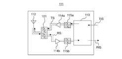
- FIG. 13 is a block diagram showing a main part of a communication apparatus 111 as an example of use of the filter device 1 (branching filter 101).
- the communication device 111 performs wireless communication using radio waves, and includes a branching filter 101 .
- a transmission information signal TIS including information to be transmitted is modulated and frequency-increased (conversion of the carrier frequency to a high-frequency signal) by an RF-IC (Radio Frequency Integrated Circuit) 113 to form a transmission signal TS.
- the transmission signal TS is filtered by the bandpass filter 115a to remove unnecessary components outside the transmission passband, amplified by the amplifier 114a, and input to the demultiplexer 101 (transmission terminal 103). Then, the demultiplexer 101 (transmission filter 105) removes unnecessary components other than the transmission passband from the input transmission signal TS, and outputs the removed transmission signal TS from the antenna terminal 102 to the antenna 112.
- the antenna 112 converts an input electrical signal (transmission signal TS) into a radio signal (radio waves) and transmits the radio signal.
- a radio signal (radio wave) received by the antenna 112 is converted into an electric signal (received signal RS) by the antenna 112 and input to the branching filter 101 (antenna terminal 102).
- the demultiplexer 101 removes unnecessary components outside the pass band for reception from the input received signal RS, and outputs the signal from the receiving terminal 104 to the amplifier 114b.
- the output reception signal RS is amplified by an amplifier 114b, and unnecessary components outside the passband for reception are removed by a bandpass filter 115b. Then, the reception signal RS is subjected to frequency reduction and demodulation by the RF-IC 113 to become a reception information signal RIS.
- the transmission information signal TIS and the reception information signal RIS may be low-frequency signals (baseband signals) containing appropriate information, such as analog audio signals or digitized audio signals.
- the passband of the radio signal may be set as appropriate, and in this embodiment, a relatively high frequency passband (eg, 5 GHz or higher) is also possible.
- the modulation method may be phase modulation, amplitude modulation, frequency modulation, or a combination of two or more of these.
- the direct conversion system is exemplified as the circuit system, but other appropriate systems may be used, such as a double superheterodyne system.
- FIG. 13 schematically shows only the main part, and a low-pass filter, isolator, or the like may be added at an appropriate position, or the position of the amplifier or the like may be changed.
- ⁇ Eulerian angles of LN (including angles equivalent to those shown below) ⁇ : -30° to 30°, 0° ⁇ 10°, or 0° ⁇ 1° ⁇ : 0° to 60°, 15° ⁇ 10°, or 15° ⁇ 1° ⁇ : -30° to 30°, 0° ⁇ 10°, or 0° ⁇ 1°
- 0° ⁇ 10° indicates ⁇ 10° or more and 10° or less.
- - Electrode material 70% or more, 90% or more, or 95% or more of the thickness (and/or volume) is Al or an Al--Cu alloy. Cu is 10 wt% or less, 5 wt% or less, or 1 wt% or less.
- Electrode thickness 50 nm to 400 nm, 100 nm to 200 nm, or 100 nm to 150 nm
- Piezoelectric film thickness 300 nm to 600 nm, 400 nm to 500 nm, or 450 nm to 500 nm
- Electrode finger pitch 0.8 ⁇ m 3.0 ⁇ m or more, 0.8 ⁇ m or more and 2.0 ⁇ m or less, or 0.8 ⁇ m or more and 1.5 ⁇ m or less, ⁇ Duty: 0.2 or more and 0.7 or less
Landscapes
- Physics & Mathematics (AREA)
- Acoustics & Sound (AREA)
- Engineering & Computer Science (AREA)
- Power Engineering (AREA)
- Computer Networks & Wireless Communication (AREA)
- Signal Processing (AREA)
- Chemical & Material Sciences (AREA)
- Materials Engineering (AREA)
- Surface Acoustic Wave Elements And Circuit Networks Thereof (AREA)
Priority Applications (3)
| Application Number | Priority Date | Filing Date | Title |
|---|---|---|---|
| CN202380016032.8A CN118489213A (zh) | 2022-01-07 | 2023-01-06 | 滤波器设备、分波器以及通信装置 |
| US18/726,867 US20250105822A1 (en) | 2022-01-07 | 2023-01-06 | Filter device, splitter, and communication device |
| JP2023572489A JPWO2023132354A1 (https=) | 2022-01-07 | 2023-01-06 |
Applications Claiming Priority (2)
| Application Number | Priority Date | Filing Date | Title |
|---|---|---|---|
| JP2022001787 | 2022-01-07 | ||
| JP2022-001787 | 2022-01-07 |
Publications (1)
| Publication Number | Publication Date |
|---|---|
| WO2023132354A1 true WO2023132354A1 (ja) | 2023-07-13 |
Family
ID=87073710
Family Applications (1)
| Application Number | Title | Priority Date | Filing Date |
|---|---|---|---|
| PCT/JP2023/000139 Ceased WO2023132354A1 (ja) | 2022-01-07 | 2023-01-06 | フィルタデバイス、分波器および通信装置 |
Country Status (4)
| Country | Link |
|---|---|
| US (1) | US20250105822A1 (https=) |
| JP (1) | JPWO2023132354A1 (https=) |
| CN (1) | CN118489213A (https=) |
| WO (1) | WO2023132354A1 (https=) |
Families Citing this family (1)
| Publication number | Priority date | Publication date | Assignee | Title |
|---|---|---|---|---|
| JP2024017316A (ja) * | 2022-07-27 | 2024-02-08 | 株式会社村田製作所 | 高周波モジュール |
Citations (3)
| Publication number | Priority date | Publication date | Assignee | Title |
|---|---|---|---|---|
| WO2005055423A1 (ja) * | 2003-12-01 | 2005-06-16 | Murata Manufacturing Co., Ltd. | フィルタ装置 |
| WO2018047862A1 (ja) * | 2016-09-07 | 2018-03-15 | 株式会社村田製作所 | 弾性波フィルタ装置及び複合フィルタ装置 |
| WO2019138810A1 (ja) * | 2018-01-12 | 2019-07-18 | 株式会社村田製作所 | 弾性波装置、マルチプレクサ、高周波フロントエンド回路及び通信装置 |
Family Cites Families (1)
| Publication number | Priority date | Publication date | Assignee | Title |
|---|---|---|---|---|
| JP7352855B2 (ja) * | 2019-08-21 | 2023-09-29 | 株式会社村田製作所 | 分波器 |
-
2023
- 2023-01-06 CN CN202380016032.8A patent/CN118489213A/zh active Pending
- 2023-01-06 US US18/726,867 patent/US20250105822A1/en active Pending
- 2023-01-06 WO PCT/JP2023/000139 patent/WO2023132354A1/ja not_active Ceased
- 2023-01-06 JP JP2023572489A patent/JPWO2023132354A1/ja active Pending
Patent Citations (3)
| Publication number | Priority date | Publication date | Assignee | Title |
|---|---|---|---|---|
| WO2005055423A1 (ja) * | 2003-12-01 | 2005-06-16 | Murata Manufacturing Co., Ltd. | フィルタ装置 |
| WO2018047862A1 (ja) * | 2016-09-07 | 2018-03-15 | 株式会社村田製作所 | 弾性波フィルタ装置及び複合フィルタ装置 |
| WO2019138810A1 (ja) * | 2018-01-12 | 2019-07-18 | 株式会社村田製作所 | 弾性波装置、マルチプレクサ、高周波フロントエンド回路及び通信装置 |
Also Published As
| Publication number | Publication date |
|---|---|
| US20250105822A1 (en) | 2025-03-27 |
| CN118489213A (zh) | 2024-08-13 |
| JPWO2023132354A1 (https=) | 2023-07-13 |
Similar Documents
| Publication | Publication Date | Title |
|---|---|---|
| JP6481758B2 (ja) | 弾性波フィルタ、マルチプレクサ、デュプレクサ、高周波フロントエンド回路、および通信装置 | |
| JP6637990B2 (ja) | 弾性波共振子、弾性波フィルタ、分波器、通信装置および弾性波共振子の設計方法 | |
| US10958241B2 (en) | Extractor | |
| JP6870684B2 (ja) | マルチプレクサ | |
| JP2017152881A (ja) | マルチプレクサ、送信装置および受信装置 | |
| WO2019017422A1 (ja) | マルチプレクサ、高周波フロントエンド回路および通信装置 | |
| CN110809858B (zh) | 多工器 | |
| WO2020105589A1 (ja) | エクストラクタ | |
| JP7793060B2 (ja) | 弾性波共振子、弾性波フィルタおよび通信装置 | |
| US10651822B2 (en) | Multiplexer | |
| JP7117880B2 (ja) | 弾性波フィルタ、分波器および通信装置 | |
| JP7386741B2 (ja) | フィルタ、分波器及び通信装置 | |
| JP7103420B2 (ja) | フィルタ装置およびマルチプレクサ | |
| WO2023132354A1 (ja) | フィルタデバイス、分波器および通信装置 | |
| WO2019172032A1 (ja) | マルチプレクサ、高周波フロントエンド回路および通信装置 | |
| WO2024101346A1 (ja) | 複合フィルタ、モジュール及び通信装置 | |
| WO2023033032A1 (ja) | 弾性波素子、分波器および通信装置 | |
| WO2024190677A1 (ja) | 弾性波共振子および通信装置 | |
| WO2018212025A1 (ja) | マルチプレクサ、送信装置および受信装置 | |
| JP2025043942A (ja) | 弾性波装置およびマルチプレクサ | |
| JP2025097818A (ja) | 弾性波フィルタ | |
| JP2024104398A (ja) | マルチプレクサ | |
| JP2025056812A (ja) | 弾性波装置、分波器、通信装置および弾性波装置の製造方法 | |
| JP2024162470A (ja) | マルチプレクサ | |
| WO2023054301A1 (ja) | 弾性波フィルタ装置およびマルチプレクサ |
Legal Events
| Date | Code | Title | Description |
|---|---|---|---|
| 121 | Ep: the epo has been informed by wipo that ep was designated in this application |
Ref document number: 23737305 Country of ref document: EP Kind code of ref document: A1 |
|
| WWE | Wipo information: entry into national phase |
Ref document number: 202380016032.8 Country of ref document: CN |
|
| ENP | Entry into the national phase |
Ref document number: 2023572489 Country of ref document: JP Kind code of ref document: A |
|
| WWE | Wipo information: entry into national phase |
Ref document number: 18726867 Country of ref document: US |
|
| NENP | Non-entry into the national phase |
Ref country code: DE |
|
| 122 | Ep: pct application non-entry in european phase |
Ref document number: 23737305 Country of ref document: EP Kind code of ref document: A1 |
|
| WWP | Wipo information: published in national office |
Ref document number: 18726867 Country of ref document: US |