WO2023120337A1 - 銅箔の表面パラメータの測定方法、及び銅箔の選別方法 - Google Patents
銅箔の表面パラメータの測定方法、及び銅箔の選別方法 Download PDFInfo
- Publication number
- WO2023120337A1 WO2023120337A1 PCT/JP2022/046102 JP2022046102W WO2023120337A1 WO 2023120337 A1 WO2023120337 A1 WO 2023120337A1 JP 2022046102 W JP2022046102 W JP 2022046102W WO 2023120337 A1 WO2023120337 A1 WO 2023120337A1
- Authority
- WO
- WIPO (PCT)
- Prior art keywords
- copper foil
- filter
- sdr
- less
- value
- Prior art date
- Legal status (The legal status is an assumption and is not a legal conclusion. Google has not performed a legal analysis and makes no representation as to the accuracy of the status listed.)
- Ceased
Links
Images







Classifications
-
- G—PHYSICS
- G01—MEASURING; TESTING
- G01B—MEASURING LENGTH, THICKNESS OR SIMILAR LINEAR DIMENSIONS; MEASURING ANGLES; MEASURING AREAS; MEASURING IRREGULARITIES OF SURFACES OR CONTOURS
- G01B11/00—Measuring arrangements characterised by the use of optical techniques
- G01B11/30—Measuring arrangements characterised by the use of optical techniques for measuring roughness or irregularity of surfaces
-
- G—PHYSICS
- G01—MEASURING; TESTING
- G01B—MEASURING LENGTH, THICKNESS OR SIMILAR LINEAR DIMENSIONS; MEASURING ANGLES; MEASURING AREAS; MEASURING IRREGULARITIES OF SURFACES OR CONTOURS
- G01B21/00—Measuring arrangements or details thereof, where the measuring technique is not covered by the other groups of this subclass, unspecified or not relevant
- G01B21/30—Measuring arrangements or details thereof, where the measuring technique is not covered by the other groups of this subclass, unspecified or not relevant for measuring roughness or irregularity of surfaces
-
- G—PHYSICS
- G01—MEASURING; TESTING
- G01B—MEASURING LENGTH, THICKNESS OR SIMILAR LINEAR DIMENSIONS; MEASURING ANGLES; MEASURING AREAS; MEASURING IRREGULARITIES OF SURFACES OR CONTOURS
- G01B9/00—Measuring instruments characterised by the use of optical techniques
- G01B9/04—Measuring microscopes
-
- G—PHYSICS
- G01—MEASURING; TESTING
- G01N—INVESTIGATING OR ANALYSING MATERIALS BY DETERMINING THEIR CHEMICAL OR PHYSICAL PROPERTIES
- G01N21/00—Investigating or analysing materials by the use of optical means, i.e. using sub-millimetre waves, infrared, visible or ultraviolet light
- G01N21/84—Systems specially adapted for particular applications
- G01N21/88—Investigating the presence of flaws or contamination
- G01N21/95—Investigating the presence of flaws or contamination characterised by the material or shape of the object to be examined
- G01N21/956—Inspecting patterns on the surface of objects
-
- G—PHYSICS
- G01—MEASURING; TESTING
- G01N—INVESTIGATING OR ANALYSING MATERIALS BY DETERMINING THEIR CHEMICAL OR PHYSICAL PROPERTIES
- G01N21/00—Investigating or analysing materials by the use of optical means, i.e. using sub-millimetre waves, infrared, visible or ultraviolet light
- G01N21/84—Systems specially adapted for particular applications
- G01N21/88—Investigating the presence of flaws or contamination
- G01N21/95—Investigating the presence of flaws or contamination characterised by the material or shape of the object to be examined
- G01N21/956—Inspecting patterns on the surface of objects
- G01N21/95623—Inspecting patterns on the surface of objects using a spatial filtering method
-
- G—PHYSICS
- G01—MEASURING; TESTING
- G01N—INVESTIGATING OR ANALYSING MATERIALS BY DETERMINING THEIR CHEMICAL OR PHYSICAL PROPERTIES
- G01N21/00—Investigating or analysing materials by the use of optical means, i.e. using sub-millimetre waves, infrared, visible or ultraviolet light
- G01N21/84—Systems specially adapted for particular applications
- G01N21/88—Investigating the presence of flaws or contamination
- G01N21/95—Investigating the presence of flaws or contamination characterised by the material or shape of the object to be examined
- G01N21/956—Inspecting patterns on the surface of objects
- G01N2021/95638—Inspecting patterns on the surface of objects for PCB's
-
- H—ELECTRICITY
- H05—ELECTRIC TECHNIQUES NOT OTHERWISE PROVIDED FOR
- H05K—PRINTED CIRCUITS; CASINGS OR CONSTRUCTIONAL DETAILS OF ELECTRIC APPARATUS; MANUFACTURE OF ASSEMBLAGES OF ELECTRICAL COMPONENTS
- H05K1/00—Printed circuits
- H05K1/02—Details
- H05K1/0213—Electrical arrangements not otherwise provided for
- H05K1/0237—High frequency adaptations
Definitions
- the present invention relates to a method for measuring surface parameters of copper foils and a method for sorting copper foils.
- copper foil is widely used in the form of copper-clad laminates laminated with insulating resin substrates.
- the copper foil and the insulating resin base material have high adhesive strength in order to prevent the wiring from being peeled off during the production of the printed wiring board. Therefore, in general copper foil for printed wiring board manufacturing, surface treatment such as roughening treatment is applied to the bonding surface of the copper foil to form unevenness composed of fine copper particles, and the unevenness is formed by pressing to form an insulating resin base material. Adhesion is improved by making it bite into the inside and exerting an anchor effect.
- a printed wiring board is provided with a copper foil processed into a wiring pattern and an insulating base material. losses.
- Patent Document 1 Japanese Patent Application Laid-Open No. 2020-50954
- Patent Document 1 Japanese Patent Application Laid-Open No. 2020-50954
- a micro-roughened electrodeposited copper foil is disclosed, which is said to effectively suppress loss during signal transport.
- Non-Patent Document 1 High-speed transmission line test method guideline for flexible printed wiring boards, 1st edition describes a test method by a three-dimensional method for a copper foil surface profile for high-frequency transmission lines. is disclosed.
- Non-Patent Document 1 describes that the average height Sa is calculated.
- the surface parameters calculated by the conventional copper foil surface roughness measurement method did not necessarily have a sufficient correlation with the high-frequency characteristics. Therefore, it is necessary to prepare a surface-treated copper foil and actually evaluate its high-frequency characteristics, which requires a waste of work time and materials.
- the present inventors set the cutoff value of the L filter so as to satisfy a predetermined condition based on the surface profile of the surface-treated copper foil as a reference, and then set the surface of the surface-treated copper foil as the measurement target.
- the inventors have found that by processing the profile with an L filter having a preset cutoff value, it is possible to easily obtain a surface parameter that exhibits a high correlation with high-frequency characteristics.
- an object of the present invention is to provide a measurement method that can easily acquire surface parameters of copper foil that show a high correlation with high-frequency characteristics.
- a method for measuring a surface parameter of a copper foil comprising: (a) acquiring a surface profile on the treated surface of the surface-treated copper foil as a reference for setting filter conditions; (b) setting a cutoff value for an L filter based on said surface profile, said cutoff value being: (i) Sa1, which is the arithmetic mean height Sa after processing with the L filter, is 0.5 ⁇ m or less, and (ii) Rate of change in the developed area ratio Sdr of the interface before and after treatment with the L filter: (
- a copper foil sorting method comprising: A step of measuring surface parameters of a copper foil using the method according to any one of aspects 1 to 5, wherein the surface parameters are an arithmetic mean height Sa and a root mean square height Sq defined by ISO 25178 , the maximum height Sz, the developed area ratio Sdr of the interface, the substantial volume Vmc of the core portion, and the level difference Sk of the core portion.
- the surface parameters are an arithmetic mean height Sa and a root mean square height Sq defined by ISO 25178 , the maximum height Sz, the developed area ratio Sdr of the interface, the substantial volume Vmc of the core portion, and the level difference Sk of the core portion.
- a step of selecting the copper foil as a copper foil suitable for a printed wiring board for high frequency applications comprising: [Aspect 7] A method for manufacturing a printed wiring board for high frequency applications, comprising a step of manufacturing a printed wiring board for high frequency applications using the copper foil obtained by the method according to aspect 6.
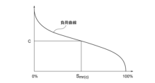
- FIG. 4 is a diagram for explaining a load curve and a load area ratio determined according to ISO25178
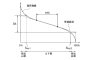
- FIG. 10 is a diagram for explaining a load area ratio Smr1 for separating the protruding peak portion and the core portion, a load area ratio Smr2 for separating the protruding valley portion and the core portion, and a level difference Sk between the core portions, which are determined in accordance with ISO25178; be.
- FIG. 10 is a diagram for explaining a substantial volume Vmc of a core portion determined in accordance with ISO25178
- FIG. 4 is a schematic diagram of a copper foil surface having a plurality of bumps, and is a diagram for explaining the ⁇ value.
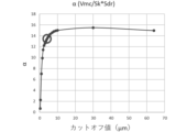
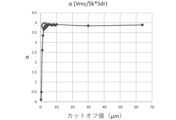
- 10 is a graph showing the ⁇ value of the treated surface of the copper foil d subjected to L filter treatment with each cutoff value in Example A1.
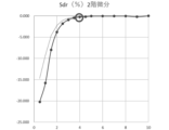
- 10 is a graph showing the second derivative of Sdr before and after L filter treatment on the treated surface of copper foil d.
- 4 is a graph showing the Sdr of the treated surface of the copper foil e subjected to L filter treatment with each cutoff value in Example A1.
- 10 is a graph showing the ⁇ value of the treated surface of the copper foil e subjected to L filter treatment with each cutoff value in Example A1.
- 10 is a graph showing the second derivative of Sdr before and after L filter treatment on the treated surface of copper foil e.
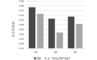
- 4 is a graph comparing coefficients of determination R2 of regression equations for surface parameters of copper foils and transmission loss in Examples A1 to A3.
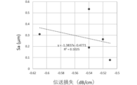
- 4 is a graph showing the correlation between the arithmetic mean height Sa of copper foils a to e and high frequency characteristics in Example B1.
- 10 is a graph showing the correlation (coefficient of determination R 2 ) between the change rate of Sdr of copper foils a to e and the high-frequency characteristics in Examples B2 to B8.
- 10 is a graph showing the correlation (coefficient of determination R 2 ) between the change rate of the ⁇ value of copper foils a to e and the high-frequency characteristics in Examples B2 to B8.
- 10 is a graph showing the correlation between the arithmetic mean height Sa of the copper foils a to e and the high frequency characteristics in Example B3.
- Arithmetic mean height Sa or "Sa” as used herein is a parameter that represents the average of the absolute values of the height difference at each point with respect to the average plane of the surface defined in ISO25178. That is, Sa corresponds to a parameter obtained by extending the arithmetic mean height Ra of the contour curve to the surface.
- the "root mean square height Sq" or “Sq” is a parameter corresponding to the standard deviation of the distance from the average plane defined in ISO25178, and corresponds to the standard deviation of height.
- Maximum height Sz or “Sz” as used herein represents the distance from the highest point to the lowest point on the surface as defined in ISO25178.
- the term "developed area ratio Sdr” or “Sdr” of the interface represents how much the developed area (surface area) of the defined region increases with respect to the area of the defined region, as defined in ISO25178. is a parameter.
- the developed area ratio Sdr of the interface is expressed as an increase (%) of the surface area. The smaller this value, the more nearly flat the surface shape is, and the Sdr of a completely flat surface is 0%. On the other hand, the larger this value, the more uneven the surface shape. For example, if the Sdr of a surface is 40%, then this surface represents a 40% increase in surface area from a perfectly flat surface.
- the "surface load curve” (hereinafter simply referred to as "load curve”) refers to a curve that expresses the height at which the load area ratio is from 0% to 100%, as defined in ISO25178.
- the load area ratio is a parameter representing the area of a region having a certain height c or more, as shown in FIG.
- the load area ratio at height c corresponds to Smr(c) in FIG.
- the secant line of the load curve drawn from the load area ratio of 0% along the load curve with the difference in the load area ratio of 40% is moved from the load area ratio of 0% to the secant line.
- the point where the slope of is the gentlest is called the central portion of the load curve.
- a straight line that minimizes the sum of squares of deviations in the direction of the vertical axis with respect to the central portion is called an equivalent straight line.
- a portion included in the height range of the load area ratio of 0% to 100% of the equivalent straight line is called a core portion.
- a portion higher than the core portion is called a protruding peak portion, and a portion lower than the core portion is called a protruding valley portion.
- the “core portion level difference Sk” or “Sk” is a value obtained by subtracting the minimum height from the maximum height of the core portion defined in ISO 25178, and as shown in FIG. This parameter is calculated from the difference between the heights of the equivalent straight line at the load area ratio of 0% and 100%.
- Vmc of the core is a parameter representing the volume of the core measured in accordance with ISO25178, as shown in FIG.
- Vmc is calculated by specifying a load area ratio Smr1 that separates the core portion and the protruding peak portion as 10% and a load area ratio Smr2 that separates the core portion and the protruding valley portion as 80%. .
- ⁇ value refers to the actual volume Vmc of the core portion divided by the level difference Sk of the core portion and multiplied by the developed area ratio Sdr of the interface, that is, by the formula (Vmc/Sk) ⁇ Sdr. means the parameters obtained.
- FIG. 4 shows a schematic diagram of the copper foil surface for explaining the ⁇ value.
- Vmc corresponds to the volume of the core portion obtained by removing the protrusion from the bump N
- Sk corresponds to the height of the core portion ( See FIG. 4(ii)).
- Vmc/Sk obtained by dividing Vmc by Sk corresponds to the area of the core portion (see FIG. 4(iii)), and the ⁇ value obtained by multiplying Vmc/Sk by Sdr reflects the Sdr of the core portion. It can be said that it is a parameter (see FIG. 4(iv)).
- untreated copper foil refers to copper foil that has not been subjected to surface treatment such as roughening treatment or rust prevention treatment.
- the copper foil referred to here may be a copper foil provided with a support layer, a release layer and an ultra-thin copper layer (so-called copper foil with a carrier).
- the "electrode surface” of the electrolytic copper foil refers to the surface that was in contact with the cathode during production.
- the "deposition surface" of the electrolytic copper foil refers to the surface on which electrolytic copper is deposited during production, that is, the surface that is not in contact with the cathode.
- the "L filter” is a filter that removes large wavelength components, and is also referred to as " ⁇ c" in contour curve method measurement (line roughness measurement). That is, the L filter is a filter that removes large-scale wavelength components such as waviness of the copper foil.
- the "S filter” is a filter that removes small wavelength components, and is also referred to as " ⁇ s" in contour curve method measurement (line roughness measurement). That is, the S filter is a filter that removes small-scale wavelength components such as roughening treatment of copper foil.
- the method of the present invention is a method for measuring surface parameters of copper foil. This method consists of (1) acquiring the surface profile of the reference copper foil, (2) setting the cutoff value of the L filter, (3) acquiring the surface profile of the copper foil to be measured, and (4) filtering the surface profile of the copper foil to be measured. and (5) calculation of the surface parameters of the copper foil to be measured.
- steps (1) to (5) will be described below with reference to the drawings.
- FIG. 5 shows an example of a method for measuring surface parameters of a copper foil according to the present invention.
- a surface profile on the treated surface of the surface-treated copper foil 10 is acquired as a reference in order to set filter conditions.
- the surface-treated copper foil as a reference may be called "reference copper foil.”
- Acquisition of the surface profile of the reference copper foil 10 for setting the filter conditions is preferably carried out by measuring the treated surface of the reference copper foil 10 using a non-contact surface roughness measuring instrument such as a commercially available laser microscope. can be done.
- the measurement area is preferably 90 ⁇ m 2 or more and 103,000 ⁇ m 2 or less, more preferably 1,000 ⁇ m 2 or more and 26,000 ⁇ m 2 or less, still more preferably 1,000 ⁇ m 2 or more and 17,000 ⁇ m. 2 or less.
- the measurement magnification of the laser microscope is preferably 50 times or more and 500 times or less, more preferably 100 times or more and 400 times or less.
- the reference copper foil 10 may be manufactured according to known methods and conditions, or may be a commercially available product.
- the reference copper foil 10 is obtained by subjecting at least one surface of an untreated copper foil 12 to surface treatment to form bumps 14 (for example, roughening particles). It can be produced preferably by
- the thickness of the reference copper foil 10 (referring to the thickness of the ultra-thin copper layer in the case of a copper foil with a carrier) is preferably 0.5 ⁇ m or more and 210 ⁇ m or less, more preferably 0.5 ⁇ m or more and 70 ⁇ m or less.
- the untreated copper foil 12 may be either electrolytic copper foil or rolled copper foil, preferably electrolytic copper foil.
- surface treatments applied to the untreated copper foil 12 include roughening treatment, rust prevention treatment, coupling agent treatment, and any combination thereof.
- the reference copper foil 10 is preferably provided with bumps 14 by subjecting the untreated copper foil 12 to at least roughening treatment, but only antirust treatment without roughening treatment is performed. It may be a broken one.
- the surface treatment may be performed on either the electrode surface or the deposition surface of the electrolytic copper foil.
- the cutoff value of the L filter Based on the acquired surface profile of the surface-treated copper foil 10 as a reference, the cutoff value of the L filter is set.
- the cutoff value of the L filter is set in advance in this manner, it becomes unnecessary to set the measurement conditions for each surface-treated copper foil to be measured and calculate the surface parameters.
- the unevenness on the treated surface of the surface-treated copper foil consists of a roughness component caused by bumps (roughening particles, etc.) and an undulation component caused by undulation of the copper foil.
- the transmission loss of the printed wiring board increases due to the skin effect of the copper foil, which becomes more pronounced as the frequency increases.
- the setting of the cutoff value of the L filter may be performed so as to satisfy only one of the first aspect and the second aspect described later, or may be performed so as to satisfy both.
- the cutoff value of the L filter satisfies (i) Sa1, which is Sa after processing with the L filter, is 0.5 ⁇ m or less, and (ii) processing with the L filter Change rate of Sdr before and after: (
- the cut-off value of the L filter is preferably Sa1 of 0.3 ⁇ m or less and Sdr change rate of 70% or less, more preferably Sa1 of 0.001 ⁇ m or more and 0.3 ⁇ m or less, and Sdr
- the rate of change is set to 0.1% or more and 60% or less, more preferably Sa1 is 0.005 ⁇ m or more and 0.2 ⁇ m or less, and the rate of change of Sdr is set to be 1% or more and 40% or less. That is, Sa1 is 0.5 ⁇ m or less, preferably 0.3 ⁇ m or less, more preferably 0.001 ⁇ m or more and 0.3 ⁇ m or less, and still more preferably 0.005 ⁇ m or more and 0.2 ⁇ m or less.
- the change rate of Sdr is 80% or less, preferably 70% or less, more preferably 0.1% or more and 60% or less, and still more preferably 1% or more and 40% or less.
- the rate of change of Sdr is within the above range, it is possible to reliably leave a roughness component (hump component) that greatly affects high-frequency characteristics.
- the change rate of Sdr increases. Therefore, by controlling the rate of change of Sdr within the above range, it is possible to effectively suppress the removal of the roughness component necessary for evaluating the high-frequency characteristics. Therefore, by setting the cutoff value of the L filter so as to satisfy the above conditions, it is possible to calculate the surface parameter of the surface-treated copper foil that exhibits a high correlation with the high-frequency characteristics in the process described later.
- the cutoff value of the L filter is such that (i) Sa1, which is Sa after processing with the L filter, is 0.5 ⁇ m or less, and (ii′) with the L filter Rate of change in ⁇ value before and after processing: (
- Sa1 is more preferably 0.3 ⁇ m or less, and the change rate of the ⁇ value is 70% or less, more preferably Sa1 is 0.001 ⁇ m or more and 0.3 ⁇ m or less, and The ⁇ value change rate is set to 0.1% or more and 60% or less, particularly preferably Sa1 is 0.005 ⁇ m or more and 0.2 ⁇ m or less, and the ⁇ value change rate is set to 1% or more and 40% or less. be done.
- Sa1 is preferably 0.5 ⁇ m or less, more preferably 0.3 ⁇ m or less, still more preferably 0.001 ⁇ m or more and 0.3 ⁇ m or less, and particularly preferably 0.005 ⁇ m or more and 0.2 ⁇ m or less.
- the change rate of the ⁇ value is preferably 80% or less, more preferably 70% or less, still more preferably 0.1% or more and 60% or less, and particularly preferably 1% or more and 40% or less. If the rate of change of the ⁇ value is within the above range, it is possible to reliably leave a roughness component (hump component) that greatly affects high-frequency characteristics.
- the change rate of the ⁇ value increases. Therefore, by controlling the change rate of the ⁇ value within the above range, it is possible to effectively suppress the removal of the roughness component necessary for evaluating the high-frequency characteristics. Therefore, by setting the cutoff value of the L filter so as to satisfy the above conditions, it is possible to calculate the surface parameter of the surface-treated copper foil that exhibits a high correlation with the high-frequency characteristics in the process described later.
- the cutoff value of the L filter may be set as follows. First, the surface profile of the reference copper foil 10 is analyzed tentatively using cutoff values of a plurality of L filters, and surface parameters are calculated for each cutoff value. Then, based on the calculated surface parameter, a preferable cutoff value is specified from among the plurality of cutoff values. Identification of such a cut-off value can be preferably performed, for example, by obtaining a change point according to various conditions described in the examples of this specification. In particular, from the viewpoint of setting the optimum cutoff value more reliably, it is preferable to set the cutoff value of the L filter by performing the second derivative of the surface parameter (for example, Sdr or ⁇ value) defined by ISO25178.
- the second derivative of the surface parameter for example, Sdr or ⁇ value
- the surface profile of the treated surface of the surface-treated copper foil 10' to be measured is acquired.
- the surface-treated copper foil as a measurement object may be called “measurement object copper foil.”
- This copper foil 10 ′ to be measured is manufactured or processed under the same conditions as those of the reference copper foil 10 .
- the reference copper foil 10 and the copper foil 10' to be measured have the same specifications and are products of different lots.
- the locations of the surface profiles on the treated surfaces of the reference copper foil 10 and the copper foil 10' to be measured are different from each other, both may be the same product. That is, the method of the present invention can be preferably used to confirm changes in the surface treatment state, for example, at the initial stage and the latter stage of a production lot when producing a long surface-treated copper foil such as a roll. .
- the method for measuring surface parameters of copper foil according to the present invention can be preferably used for product management, quality assurance, and the like. That is, by using the surface parameters obtained through the process of the present invention, it is possible to simply and reliably select and ship high-quality products as described later.
- the measurement of the surface profile of the copper foil 10' to be measured and the calculation of the surface parameters may be performed immediately after the copper foil 10' to be measured is manufactured, or may be performed during pre-shipment inspection. good.
- the surface profile of the copper foil 10' to be measured can be preferably obtained by measuring the surface of the copper foil 10' to be measured using a commercially available laser microscope, which is a non-contact surface roughness measuring device.
- the laser microscope for example, the conditions described above regarding the acquisition of the surface profile of the reference copper foil 10 can be adopted as they are.
- the above filtering process is preferably performed without using an S filter.
- unevenness smaller than the cutoff value of the S filter is averaged (removed). Therefore, by performing filter processing without using the S filter, it is possible to reliably detect small bumps (roughening particles, etc.) present in the copper foil 10 ′ to be measured, and as a result, the correlation with the high frequency characteristics is improved. Higher surface parameters can be calculated.
- the surface parameters calculated through the above-described process are parameters that sufficiently eliminate the influence of the waviness component and accurately reflect the roughness component of the surface-treated copper foil, so that the high-frequency characteristics can be accurately predicted. . As a result, it becomes unnecessary to actually evaluate the high-frequency characteristics each time the copper foil is produced, and it is possible to save working time and waste of materials.
- Preferred examples of surface parameters to be calculated include Sa, Sq, Sz, Sdr, Vmc, Sk, and combinations thereof (e.g., ⁇ value), more preferably Sa, Sq, Sdr, Vmc, Sk and their more preferably Sa, Sdr, Vmc, Sk and combinations thereof, particularly preferably Sa, Sdr and combinations thereof. With these surface parameters, the correlation with high-frequency characteristics is even higher.
- a method for sorting copper foil includes a step of measuring the surface parameters of the copper foil based on the above-described method, and a step of sorting out the copper foil having the predetermined surface parameter as a copper foil suitable for a printed wiring board for high frequency applications. including.
- the surface parameter of the copper foil measured in this aspect is at least one selected from the group consisting of Sa, Sq, Sz, Sdr, Vmc and Sk. Then, copper foils having surfaces with Sa, Sdr, Vmc and/or Sk within the ranges shown in Table 1 are selected as copper foils suitable for printed wiring boards for high frequency applications.
- the surface parameters of the copper foil measured by the method of the present invention have a high correlation with the high frequency characteristics, so they can be used as an alternative index for the high frequency characteristics.
- a copper foil having a surface that satisfies the surface parameters within the above ranges can be judged to be particularly excellent in high frequency characteristics, and therefore can be said to be a copper foil suitable for printed wiring boards for high frequency applications.
- a method for producing a printed wiring board for high frequency applications includes a step of manufacturing a printed wiring board for high frequency applications using the copper foil obtained by the above-described method.
- a known layer structure can be adopted for the printed wiring board. That is, except for using the surface-treated copper foil selected by the method of the present invention, the printed wiring board can be manufactured using known methods and conditions, and is not particularly limited.
- the printed wiring board manufactured by the method of the present invention is preferably used for high frequency applications of 1 GHz or higher, more preferably 3 GHz or higher, and still more preferably 20 GHz or higher and 300 GHz or lower.
- the cutoff value of the L filter was set based on the surface profile of the reference copper foil, and the correlation between the surface parameters of the copper foil to be measured and the high frequency characteristics was confirmed. Specifically, it is as follows.
- Example A1 Preparation of Reference Copper Foil First, as untreated copper foils, two types of copper foils (deposited foils) as electrolytically manufactured were prepared as follows. - Untreated copper foil I: 18 ⁇ m thick, manufactured by the method disclosed in Patent Document 2 (Japanese Patent Laid-Open No. 9-241882) - Untreated copper foil II: 18 ⁇ m thick, described in Patent Document 3 (WO2008/041706A1) Manufactured by disclosed methods
- the electrode surface or deposition surface of untreated copper foil I or II is subjected to surface treatment (roughening treatment) under known conditions to obtain a reference copper foil having a surface roughness of
- Five types of surface-treated copper foils (copper foils a to e) with different thicknesses were produced.
- the copper foils a, c, and e are roughened under different conditions on the deposition surface of the untreated copper foil II, and therefore have different surface roughnesses. All of the produced copper foils a to e have properties (surface roughness, high frequency characteristics, etc.) equivalent to those of commercially available products.
- FIG. 6A and 6B show the Sdr and ⁇ values of the copper foil b after the L filter treatment at each cutoff value
- FIG. 7 shows the second derivative of Sdr before and after the L filter treatment
- 8A and 8B show the Sdr and ⁇ values of the copper foil d after the L filter treatment with each cutoff value
- FIG. 9 shows the second derivative of Sdr before and after the L filter treatment
- 10A and 10B show the Sdr and ⁇ values of the copper foil e after the L filter treatment with each cutoff value
- FIG. 11 shows the second derivative of Sdr before and after the L filter treatment.
- the rate of change of Sdr and the rate of change of ⁇ value in copper foils a to e are both 80% or less, and Sa ( That is, it was confirmed that the values of Sa1) were all 0.5 ⁇ m or less.
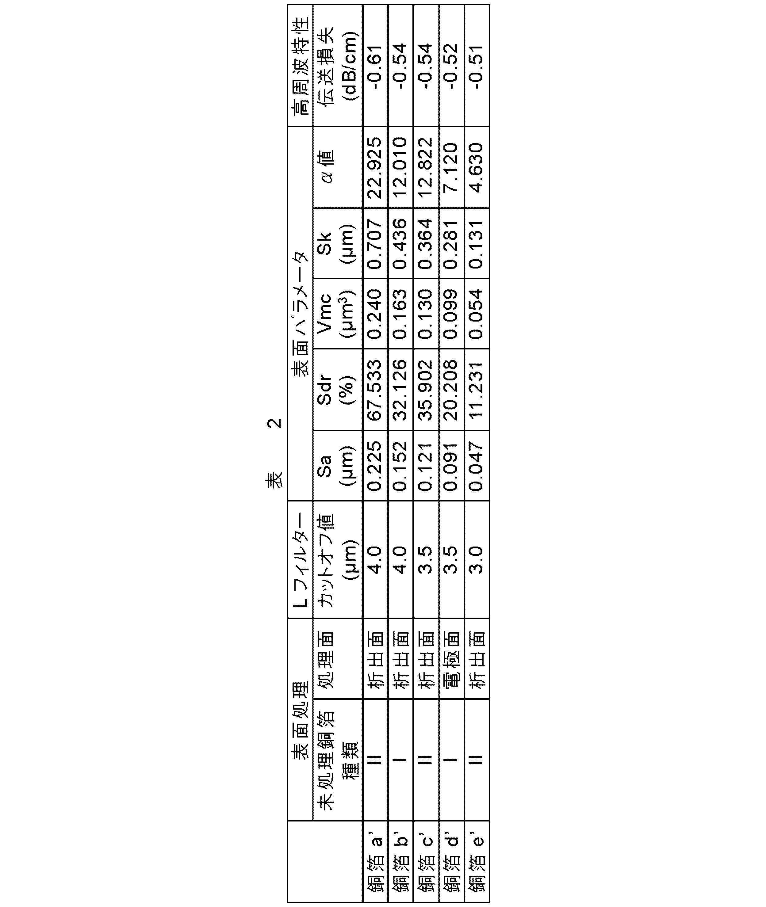
- the cutoff values of the L filter for the copper foils a to e were set as shown in Table 2, respectively.
- the term "change point” as used herein refers to a point at which the slope of the graph changes significantly in the graph showing the relationship between the cutoff value and the surface parameter (here, the Sdr and ⁇ values).
- the cut-off value When the cut-off value is set to a value smaller than the change point, it indicates that the small irregularities present on the surface are actually averaged (removed). However, since it is difficult to define the "change point” strictly and unambiguously, it is a concept that allows a certain amount of latitude.
- the "change point” was determined using the values obtained by second-order differentiation of the Sdr and ⁇ values on the treated surfaces of the copper foils a to e. A 3-section moving average was used in order to reduce the error when calculating the second derivative.
- a high-frequency substrate (MEGTRON6N manufactured by Panasonic) was prepared as an insulating resin substrate.
- Surface-treated copper foils (copper foils a′ to e′) are laminated on both sides of this insulating resin base material so that the treated surfaces come into contact with the insulating resin base material, and are pressed at a temperature of 190° C. using a vacuum press.
- Lamination was performed under the condition of a press time of 120 minutes to obtain a copper-clad laminate having an insulation thickness of 136 ⁇ m.
- the copper-clad laminate was subjected to an etching process to obtain a transmission loss measuring board on which microstrip lines were formed so as to have a characteristic impedance of 50 ⁇ .
- the transmission loss (dB/cm) at 50 GHz was measured on the obtained transmission loss measuring board using a network analyzer (N5225B manufactured by Keysight Technologies). The results were as shown in Table 2.
- Example A2 In the reference copper foils (copper foils a to e), the cutoff value of the L filter was set to 5.0 ⁇ m, that is, the copper foils to be measured (copper foils a' to e '), the correlation between surface parameters and high-frequency characteristics was confirmed in the same manner as in Example A1, except that the surface profile was filtered.
- the cutoff value of the L filter is 5.0 ⁇ m
- the rate of change of Sdr and the rate of change of the ⁇ value in the copper foils a to e are both 80% or less
- All the values of Sa that is, Sa1 were 0.5 ⁇ m or less.
- Example A1 the change point of Sdr and ⁇ value is regarded as 4.0 ⁇ m (copper foil a and copper foil b), 3.5 ⁇ m (copper foil c and copper foil d) or 3.0 ⁇ m (copper foil e). However, these are different from the set value (5.0 ⁇ m) of the cutoff value in Example A2. In this regard, as shown in FIGS.
- the cutoff value range of 3.0 ⁇ m or more and 5.0 ⁇ m or less the change in Sdr and ⁇ value is small.
- the off set value is acceptable as a change point.
- Example A3 In the reference copper foils (copper foils a to e), the cutoff value of the L filter was set to 2.0 ⁇ m, that is, the copper foils to be measured (copper foils a' to e '), the correlation between surface parameters and high-frequency characteristics was confirmed in the same manner as in Example A1, except that the surface profile was filtered.
- the cutoff value of the L filter is 2.0 ⁇ m
- the rate of change of Sdr and the rate of change of the ⁇ value in the copper foils a to e are both 80% or less
- All the values of Sa that is, Sa1 were 0.5 ⁇ m or less.
- Example A1 the change point of Sdr and ⁇ value is regarded as 4.0 ⁇ m (copper foil a and copper foil b), 3.5 ⁇ m (copper foil c and copper foil d) or 3.0 ⁇ m (copper foil e). However, these are different from the set value (2.0 ⁇ m) of the cutoff value in Example A3. In this regard, as shown in FIGS.
- the change in Sdr and ⁇ value is small.
- the off set value is acceptable as a change point.
- FIG. 12 shows a graph comparing the determination coefficient R2 of the regression equation between the surface parameter (Sdr or ⁇ value) of the copper foil and the transmission loss in Examples A1 to A3.
- the correlation between surface parameters and high frequency characteristics was good. That is, by setting the cutoff value of the L filter in advance based on predetermined conditions using the reference copper foils (copper foils a to e), the surface parameters of the copper foils to be measured (copper foils a' to e') are It was confirmed that the high-frequency characteristics were accurately reflected.
- the surface parameter calculated by setting the cutoff value individually according to the surface parameter of the reference copper foil was calculated by fixing the cutoff value of the L filter.
- the surface parameters surface parameters calculated in Examples A2 and A3
- a better correlation with high frequency characteristics was obtained.
- Example B1 (Comparison) (1) Preparation of Reference Copper Foil Five kinds of surface-treated copper foils (copper foils a to e) having different surface roughnesses were prepared as reference copper foils in the same manner as in Example A1.
- Example A1 copper foils a′ to e′ were used to prepare substrates for transmission loss measurement, and the transmission loss at 50 GHz was measured.
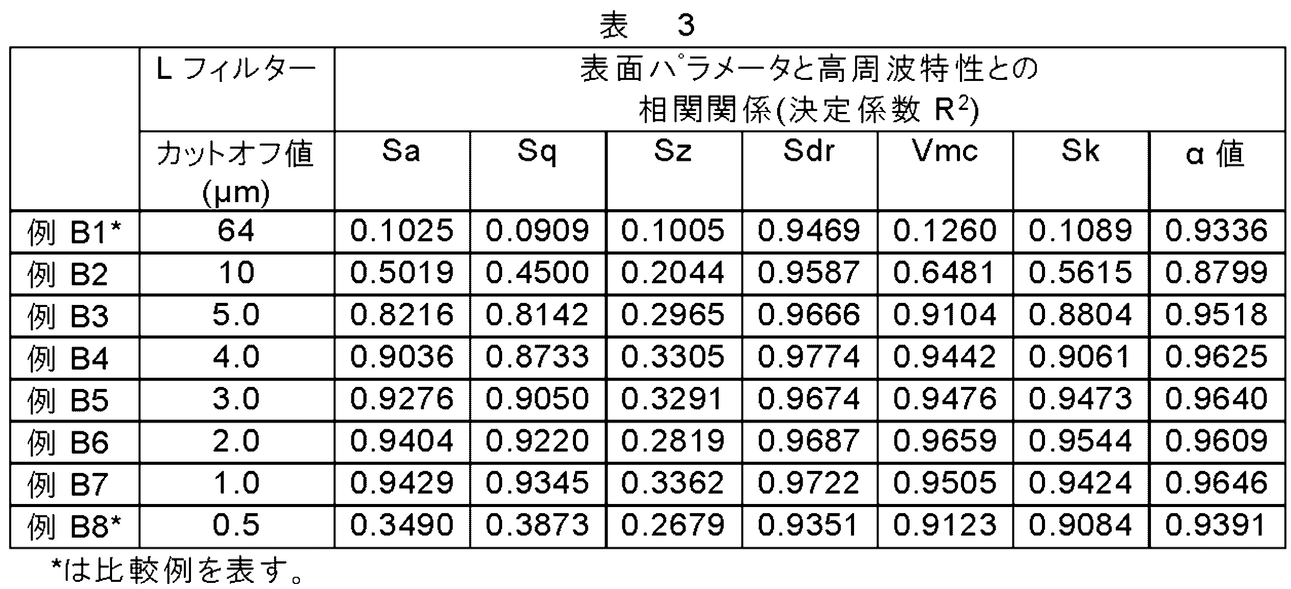
- Examples B2-B7 In the setting of the cutoff value of the L filter using the reference copper foil and the L filter treatment of the surface profile of the copper foil to be measured, the cutoff value was changed to 1.0 to 10 ⁇ m as shown in Table 3. , and confirmed the correlation between surface parameters and high-frequency characteristics in the same manner as in Example B1. The results were as shown in Table 3.
- FIG. 14 shows a graph showing the correlation (coefficient of determination R 2 ) between the rate of change in Sdr in the copper foils a to e and the high-frequency characteristics.
- a graph representing the correlation (coefficient of determination R 2 ) is shown in FIG.
- the change rate of Sdr and the change rate of ⁇ value on the treated surfaces of copper foils a to e are both 80. % or less.
- the Sa values on the treated surfaces of the copper foils a to e were all 0.5 ⁇ m or less when the cutoff value of the L filter was set to 1.0 to 10 ⁇ m.
- FIG. 16 shows a graph showing the correlation between the Sa after the L filter processing (that is, Sa1) in the copper foils a to e of Example B3 (the cutoff value of the L filter is 5 ⁇ m) and the high frequency characteristics.
- Example B8 (Comparison) In the setting of the cutoff value of the L filter using the reference copper foil and the L filter treatment of the surface profile of the copper foil to be measured, the surface was measured in the same manner as in Example B1 except that the cutoff value was changed to 0.5 ⁇ m. Correlations between parameters and high-frequency characteristics were confirmed. The results were as shown in Table 3.
- FIG. 14 shows a graph representing the correlation between the change rate of Sdr and the high-frequency characteristics (coefficient of determination R 2 ) in Example B8.
- R 2 coefficient of determination
- FIGS. 14 and 15 when the cutoff value of the L filter is 0.5 ⁇ m, the change rate of Sdr and the ⁇ value on the treated surfaces of copper foil a, copper foil b, copper foil d, and copper foil e The rate of change of was a value exceeding 80%.
- the cutoff value of the L filter was set to 0.5 ⁇ m, the Sa values on the treated surfaces of the copper foils a to e were all 0.5 ⁇ m or less.
Landscapes
- General Physics & Mathematics (AREA)
- Physics & Mathematics (AREA)
- General Health & Medical Sciences (AREA)
- Chemical & Material Sciences (AREA)
- Analytical Chemistry (AREA)
- Biochemistry (AREA)
- Life Sciences & Earth Sciences (AREA)
- Immunology (AREA)
- Pathology (AREA)
- Health & Medical Sciences (AREA)
- Electroplating Methods And Accessories (AREA)
- Length Measuring Devices With Unspecified Measuring Means (AREA)
- Manufacturing Of Printed Wiring (AREA)
- Length Measuring Devices By Optical Means (AREA)
- Investigating Materials By The Use Of Optical Means Adapted For Particular Applications (AREA)
- Analysing Materials By The Use Of Radiation (AREA)
- Investigating Or Analysing Materials By Optical Means (AREA)
- Metal Rolling (AREA)
- Electrolytic Production Of Metals (AREA)
- Investigating And Analyzing Materials By Characteristic Methods (AREA)
Abstract
Description
[態様1]
銅箔の表面パラメータの測定方法であって、
(a)フィルター条件を設定するために、リファレンスとしての表面処理銅箔の処理表面における表面プロファイルを取得する工程と、
(b)前記表面プロファイルに基づいてLフィルターのカットオフ値を設定する工程であって、前記カットオフ値は、
(i)Lフィルターで処理した後の算術平均高さSaであるSa1が0.5μm以下を満たし、かつ、
(ii)Lフィルターで処理する前後における界面の展開面積比Sdrの変化率:(|Sdr0-Sdr1|/Sdr0)×100(式中、Sdr0はLフィルターで処理する前のSdrであり、Sdr1はLフィルターで処理した後のSdrである)が80%以下を満たす、又は
(ii’)Lフィルターで処理する前後における、コア部の実体体積Vmcをコア部のレベル差Skで除して界面の展開面積比Sdrを乗じることにより、すなわち(Vmc/Sk)×Sdrの式により得られるα値の変化率:(|α0-α1|/α0)×100(式中、α0はLフィルターで処理する前のα値であり、α1はLフィルターで処理した後のα値である)が80%以下を満たすように設定され、
Sa、Sdr、Vmc及びSkはISO25178で規定される表面パラメータである、工程と、
(c)前記リファレンスとしての表面処理銅箔と同等の条件によって製造又は処理された、測定対象としての表面処理銅箔の処理表面における表面プロファイルを取得する工程と、
(d)前記測定対象としての表面処理銅箔について取得された表面プロファイルをフィルター処理する工程であって、前記カットオフ値のLフィルターを用いて処理することを含む工程と、
(e)前記フィルター処理後の表面プロファイルに基づき、前記測定対象としての表面処理銅箔の処理表面における、ISO25178で規定される表面パラメータのうち少なくとも1種を算出する工程と、
を含む、銅箔の表面パラメータの測定方法。
[態様2]
前記工程(d)において、前記フィルター処理がSフィルターを用いることなく行われる、態様1に記載の銅箔の表面パラメータの測定方法。
[態様3]
前記Sa1が0.3μm以下であり、かつ、前記Sdrの変化率が70%以下である、態様1又は2に記載の銅箔の表面パラメータの測定方法。
[態様4]
前記Sa1が0.3μm以下であり、かつ、前記α値の変化率が70%以下である、態様1~3のいずれか一つに記載の銅箔の表面パラメータの測定方法。
[態様5]
前記工程(b)において、ISO25178で規定される表面パラメータの2階微分を行い、前記Lフィルターのカットオフ値を設定する、態様1~4のいずれか一つに記載の銅箔の表面パラメータの測定方法。
[態様6]
銅箔の選別方法であって、
態様1~5のいずれか一つに記載の方法を用いて銅箔の表面パラメータを測定する工程であって、前記表面パラメータがISO25178で規定される算術平均高さSa、二乗平均平方根高さSq、最大高さSz、界面の展開面積比Sdr、コア部の実体体積Vmc及びコア部のレベル差Skからなる群から選択される少なくとも1種である工程と、
前記Saが1.2μm以下、前記Sqが2.5μm以下、前記Szが14μm以下、前記Sdrが60%以下、前記Vmcが1.5μm3以下、及び/又は前記Skが4μm以下の表面を有する銅箔を、高周波用途向けプリント配線板に適した銅箔として選別する工程と、
を含む、銅箔の選別方法。
[態様7]
態様6に記載の方法により得られた銅箔を用いて高周波用途向けプリント配線板を製造する工程を含む、高周波用途向けプリント配線板の製造方法。
本発明を特定するために用いられる用語ないしパラメータの定義を以下に示す。
本発明の方法は、銅箔の表面パラメータの測定方法である。この方法は、(1)リファレンス銅箔の表面プロファイル取得、(2)Lフィルターのカットオフ値設定、(3)測定対象銅箔の表面プロファイル取得、(4)測定対象銅箔の表面プロファイルのフィルター処理、及び(5)測定対象銅箔の表面パラメータ算出の各工程を含む。以下、図面を参照しながら、工程(1)~(5)の各々について説明する。
本発明による銅箔の表面パラメータの測定方法の一例を図5に示す。まず、図5(i)に示されるように、フィルター条件を設定するために、リファレンスとしての表面処理銅箔10の処理表面における表面プロファイルを取得する。なお、本明細書において、リファレンスとしての表面処理銅箔を「リファレンス銅箔」と称することがある。
取得したリファレンスとしての表面処理銅箔10の表面プロファイルに基づいて、Lフィルターのカットオフ値を設定する。このように予めLフィルターのカットオフ値を設定しておくことで、測定対象の表面処理銅箔ごとに測定条件を逐一設定して表面パラメータを算出することが不要となる。また、表面処理銅箔の処理表面における凹凸は、コブ(粗化粒子等)に起因する粗さ成分と、銅箔のうねりに起因するうねり成分とからなる。そして、プリント配線板の伝送損失は、高周波になるほど顕著に現れる銅箔の表皮効果によって増大するが、うねり成分は伝送損失に影響を及ぼしにくく、主に粗さ成分が伝送損失に影響を及ぼす。この点、後述する条件を満たすようにLフィルターのカットオフ値を設定することにより、高周波特性と高い相関を示す表面パラメータを簡便に取得することができる。なお、Lフィルターのカットオフ値の設定は、後述する第一の態様及び第二の態様のいずれか一方のみを満たすように行われてもよく、両方を満たすように行われてもよい。
図5(ii)に示されるように、測定対象としての表面処理銅箔10’の処理表面における表面プロファイルを取得する。なお、本明細書において、測定対象としての表面処理銅箔を「測定対象銅箔」と称することがある。この測定対象銅箔10’は、リファレンス銅箔10と同等の条件によって製造又は処理されたものである。このような例としては、リファレンス銅箔10と測定対象銅箔10’とが、互いに同一仕様で別ロットの製品である場合が挙げられる。ただし、リファレンス銅箔10及び測定対象銅箔10’の処理表面における表面プロファイルの取得箇所が互いに異なる場合、両者は同一製品であってもよい。すなわち、本発明の方法は、ロール状のように長尺の表面処理銅箔を製造する場合に、例えば製造ロットの初期及び後期における表面処理状態の変化を確認するために好ましく利用することができる。
測定対象としての表面処理銅箔10’について取得された表面プロファイルをフィルター処理する。このフィルター処理は、上述したリファレンス銅箔10の表面プロファイルに基づいて設定されたカットオフ値のLフィルターを用いて処理することを含む。こうすることで、上述のとおり高周波特性に影響を及ぼしにくい銅箔のうねり成分を選択的に除去することができ、高周波特性に大きな影響を及ぼす粗さ成分を反映した表面パラメータを算出することが可能となる。
フィルター処理後の表面プロファイルに基づき、測定対象としての表面処理銅箔10’の処理表面における、ISO25178で規定される表面パラメータのうち少なくとも1種を算出する。上述した工程を経て算出された表面パラメータは、うねり成分の影響が十分に排除され、表面処理銅箔の粗さ成分が的確に反映されたパラメータであり、それ故、高周波特性を精度良く予測できる。その結果、銅箔作製のたびに実際に高周波特性の評価を行うことが不要となり、作業時間及び材料の無駄を省くことが可能となる。
本発明の好ましい態様によれば、銅箔の選別方法が提供される。この銅箔の選別方法は、上述した方法に基づき銅箔の表面パラメータを測定する工程と、所定の表面パラメータを有する銅箔を、高周波用途向けプリント配線板に適した銅箔として選別する工程とを含む。

本発明の好ましい態様によれば、高周波用途向けプリント配線板の製造方法が提供される。このプリント配線板の製造方法は、上述した方法により得られた銅箔を用いて高周波用途向けプリント配線板を製造する工程を含む。プリント配線板は公知の層構成が採用可能である。すなわち、プリント配線板の製造は、本発明の方法により選別された表面処理銅箔を用いること以外は、公知の手法及び条件を採用することができ、特に限定されない。
本発明の方法に従って、リファレンス銅箔の表面プロファイルに基づきLフィルターのカットオフ値を設定し、測定対象銅箔の表面パラメータと高周波特性との相関関係を確認した。具体的には、以下のとおりである。
(1)リファレンス銅箔の用意
まず、未処理銅箔として、電解製箔されたままの銅箔(析離箔)を以下のとおり2種類用意した。
‐未処理銅箔I:厚さ18μm、特許文献2(特開平9-241882号公報)に開示される方法により製造
‐未処理銅箔II:厚さ18μm、特許文献3(WO2008/041706A1)に開示される方法により製造
レーザー顕微鏡(オリンパス株式会社製、OLS-5000)を用いて、測定面積4096μm2及び倍率200倍の条件で、作製した表面処理銅箔の処理表面を測定し、表面プロファイルを取得した。
得られたリファレンス銅箔の表面プロファイルを解析することにより、Sa、Sdr、Vmc及びSkを算出した。具体的には、Lフィルターのカットオフ値を0.3μm、0.5μm、1.0μm、1.5μm、2.0μm、2.5μm、3.0μm、3.5μm、4.0μm、4.5μm、5.0μm、6.0μm、7.0μm、8.0μm、9.0μm、10μm、30μm及び64μmと変更して解析を行うことで、各カットオフ値によるLフィルター処理後のSa、Sdr、Vmc及びSkを算出した。また、Lフィルターによるカットオフを行わない条件でのSdr、Vmc及びSkも同様に算出した。算出されたSdr、Vmc及びSkに基づき、α値(=(Vmc/Sk)×Sdr)を計算するとともに、Lフィルター処理前後におけるSdrの2階微分及びα値の2階微分を計算した。参考のため、銅箔bにおける、各カットオフ値によるLフィルター処理後のSdr及びα値を図6A及び6Bにそれぞれ示すとともに、Lフィルター処理前後におけるSdrの2階微分を図7に示す。また、銅箔dにおける、各カットオフ値によるLフィルター処理後のSdr及びα値を図8A及び8Bにそれぞれ示すとともに、Lフィルター処理前後におけるSdrの2階微分を図9に示す。さらに、銅箔eにおける、各カットオフ値によるLフィルター処理後のSdr及びα値を図10A及び10Bにそれぞれ示すとともに、Lフィルター処理前後におけるSdrの2階微分を図11に示す。
上記(1)で作製したリファレンス銅箔(銅箔a~e)と同一の条件を用いて、測定対象銅箔としての5種類の表面処理銅箔(銅箔a’~e’)をそれぞれ作製した。
レーザー顕微鏡(オリンパス株式会社製、OLS-5000)を用いて、測定面積4096μm2及び倍率200倍の条件で測定対象銅箔の処理表面を測定し、表面プロファイルを取得した。
各測定対象銅箔の表面プロファイルをフィルター処理した。このとき、表2に示されるとおり、Lフィルターのカットオフ値を上記(3)で設定した数値、すなわち銅箔a及び銅箔bについては4.0μm、銅箔c及びdについては3.5μm、銅箔eについては3.0μmとした。このフィルター処理は、Sフィルターによる処理は行わず、Lフィルターによる処理のみを行った。フィルター処理後の表面プロファイルに基づき、Sa、Sdr、Vmc及びSkを算出するとともに、α値を計算した。結果は表2に示されるとおりであった。
絶縁樹脂基材として高周波用基材(パナソニック製、MEGTRON6N)を用意した。この絶縁樹脂基材の両面に表面処理銅箔(銅箔a’~e’)をその処理表面が絶縁樹脂基材と当接するように積層し、真空プレス機を使用して、温度190℃、プレス時間120分の条件で積層し、絶縁厚さ136μmの銅張積層板を得た。その後、当該銅張積層板にエッチング加工を施し、特性インピーダンスが50Ωになるようマイクロストリップラインを形成した伝送損失測定用基板を得た。得られた伝送損失測定用基板に対して、ネットワークアナライザー(キーサイトテクノロジー製、N5225B)を用いて、50GHzの伝送損失(dB/cm)を測定した。結果は表2に示されるとおりであった。
伝送損失を横軸とし、表面パラメータ(Sdr又はα値)を縦軸として、各銅箔の評価結果をプロットした。このプロットデータに基づき、線形近似(最小二乗法)により回帰式を求めるとともに、決定係数R2を算出した。その結果、Sdrを縦軸とした場合の回帰式における決定係数R2は0.9786であり、α値を縦軸とした場合の回帰式における決定係数R2は0.9717であった。
リファレンス銅箔(銅箔a~e)において、Lフィルターのカットオフ値を5.0μmと設定したこと、すなわちLフィルターのカットオフ値を5.0μmとして測定対象銅箔(銅箔a’~e’)における表面プロファイルのフィルター処理を行ったこと以外は、例A1と同様にして表面パラメータ及び高周波特性の相関関係を確認した。ここで、Lフィルターのカットオフ値を5.0μmとしたときに、銅箔a~eにおけるSdrの変化率及びα値の変化率はいずれも80%以下であり、かつ、Lフィルター処理後のSa(つまりSa1)の値はいずれも0.5μm以下であった。
リファレンス銅箔(銅箔a~e)において、Lフィルターのカットオフ値を2.0μmと設定したこと、すなわちLフィルターのカットオフ値を2.0μmとして測定対象銅箔(銅箔a’~e’)における表面プロファイルのフィルター処理を行ったこと以外は、例A1と同様にして表面パラメータ及び高周波特性の相関関係を確認した。ここで、Lフィルターのカットオフ値を2.0μmとしたときに、銅箔a~eにおけるSdrの変化率及びα値の変化率はいずれも80%以下であり、かつ、Lフィルター処理後のSa(つまりSa1)の値はいずれも0.5μm以下であった。
Lフィルターのカットオフ値を変更することで、所定の条件を満たす場合に表面処理銅箔の表面パラメータが高周波特性と高い相関を示すことを確認した。具体的には、以下のとおりである。
(1)リファレンス銅箔の用意
例A1と同様にして、表面粗さの異なる5種類の表面処理銅箔(銅箔a~e)をリファレンス銅箔として用意した。
例A1と同様にして、リファレンス銅箔の処理表面における表面プロファイルを取得した。
得られたリファレンス銅箔の各表面プロファイルについて、Lフィルターのカットオフ値を64μmとして解析を行うことで、Sa、Sdr、Vmc及びSkを算出した。その結果、銅箔bにおけるLフィルター処理後のSa(すなわちSa1)が0.5μmを超える値であることが確認された。また、Lフィルターによるカットオフを行わない条件でのSdr、Vmc及びSkを算出した。算出されたSdr、Vmc及びSkに基づき、α値(=(Vmc/Sk)×Sdr)を計算するとともに、Lフィルター処理前後におけるSdrの変化率、及びα値の変化率を計算した。その結果、銅箔a~eは、いずれもSdrの変化率及びα値の変化率が80%以下であった。
例A1と同様にして、表面粗さの異なる5種類の表面処理銅箔(銅箔a’~e’)を測定対象銅箔として用意した。
例A1と同様にして、測定対象銅箔の処理表面をレーザー顕微鏡で測定し、表面プロファイルを取得した。
各銅箔の表面プロファイルをフィルター処理した。このとき、Lフィルターのカットオフ値は64μmとした。このフィルター処理は、Sフィルターによる処理は行わず、Lフィルターによる処理のみを行った。フィルター処理後の表面プロファイルに基づき、Sa、Sq、Sz、Sdr、Vmc及びSkを算出するとともに、α値を計算した。
例A1と同様にして、銅箔a’~e’を用いて伝送損失測定用基板をそれぞれ作製し、50GHzの伝送損失を測定した。
伝送損失を横軸とし、表面パラメータ(Sa、Sq、Sz、Sdr、Vmc、Sk又はα値)を縦軸として、各銅箔の評価結果をプロットした。このプロットデータに基づき、線形近似(最小二乗法)により回帰式を求めるとともに、決定係数R2を算出した。結果は表3に示されるとおりであった。参考のため、銅箔a~eにおけるSaと高周波特性との相関関係を表すグラフを図13に示す。
リファレンス銅箔を用いたLフィルターのカットオフ値の設定、及び測定対象銅箔における表面プロファイルのLフィルター処理において、表3に示すようにカットオフ値を1.0~10μmに変更したこと以外は、例B1と同様にして表面パラメータと高周波特性との相関関係を確認した。結果は表3に示されるとおりであった。
リファレンス銅箔を用いたLフィルターのカットオフ値の設定、及び測定対象銅箔における表面プロファイルのLフィルター処理において、カットオフ値を0.5μmに変更したこと以外は、例B1と同様にして表面パラメータと高周波特性との相関関係を確認した。結果は表3に示されるとおりであった。
Claims (7)
- 銅箔の表面パラメータの測定方法であって、
(a)フィルター条件を設定するために、リファレンスとしての表面処理銅箔の処理表面における表面プロファイルを取得する工程と、
(b)前記表面プロファイルに基づいてLフィルターのカットオフ値を設定する工程であって、前記カットオフ値は、
(i)Lフィルターで処理した後の算術平均高さSaであるSa1が0.5μm以下を満たし、かつ、
(ii)Lフィルターで処理する前後における界面の展開面積比Sdrの変化率:(|Sdr0-Sdr1|/Sdr0)×100(式中、Sdr0はLフィルターで処理する前のSdrであり、Sdr1はLフィルターで処理した後のSdrである)が80%以下を満たす、又は
(ii’)Lフィルターで処理する前後における、コア部の実体体積Vmcをコア部のレベル差Skで除して界面の展開面積比Sdrを乗じることにより、すなわち(Vmc/Sk)×Sdrの式により得られるα値の変化率:(|α0-α1|/α0)×100(式中、α0はLフィルターで処理する前のα値であり、α1はLフィルターで処理した後のα値である)が80%以下を満たすように設定され、
Sa、Sdr、Vmc及びSkはISO25178で規定される表面パラメータである、工程と、
(c)前記リファレンスとしての表面処理銅箔と同等の条件によって製造又は処理された、測定対象としての表面処理銅箔の処理表面における表面プロファイルを取得する工程と、
(d)前記測定対象としての表面処理銅箔について取得された表面プロファイルをフィルター処理する工程であって、前記カットオフ値のLフィルターを用いて処理することを含む工程と、
(e)前記フィルター処理後の表面プロファイルに基づき、前記測定対象としての表面処理銅箔の処理表面における、ISO25178で規定される表面パラメータのうち少なくとも1種を算出する工程と、
を含む、銅箔の表面パラメータの測定方法。 - 前記工程(d)において、前記フィルター処理がSフィルターを用いることなく行われる、請求項1に記載の銅箔の表面パラメータの測定方法。
- 前記Sa1が0.3μm以下であり、かつ、前記Sdrの変化率が70%以下である、請求項1又は2に記載の銅箔の表面パラメータの測定方法。
- 前記Sa1が0.3μm以下であり、かつ、前記α値の変化率が70%以下である、請求項1又は2に記載の銅箔の表面パラメータの測定方法。
- 前記工程(b)において、ISO25178で規定される表面パラメータの2階微分を行い、前記Lフィルターのカットオフ値を設定する、請求項1又は2に記載の銅箔の表面パラメータの測定方法。
- 銅箔の選別方法であって、
請求項1又は2に記載の方法を用いて銅箔の表面パラメータを測定する工程であって、前記表面パラメータがISO25178で規定される算術平均高さSa、二乗平均平方根高さSq、最大高さSz、界面の展開面積比Sdr、コア部の実体体積Vmc及びコア部のレベル差Skからなる群から選択される少なくとも1種である工程と、
前記Saが1.2μm以下、前記Sqが2.5μm以下、前記Szが14μm以下、前記Sdrが60%以下、前記Vmcが1.5μm3以下、及び/又は前記Skが4μm以下の表面を有する銅箔を、高周波用途向けプリント配線板に適した銅箔として選別する工程と、
を含む、銅箔の選別方法。 - 請求項6に記載の方法により得られた銅箔を用いて高周波用途向けプリント配線板を製造する工程を含む、高周波用途向けプリント配線板の製造方法。
Priority Applications (4)
| Application Number | Priority Date | Filing Date | Title |
|---|---|---|---|
| JP2023562766A JP7387085B2 (ja) | 2021-12-22 | 2022-12-14 | 銅箔の表面パラメータの測定方法、及び銅箔の選別方法 |
| CN202280059044.4A CN117881942B (zh) | 2021-12-22 | 2022-12-14 | 铜箔的表面参数的测定方法以及铜箔的筛选方法 |
| US18/714,993 US12399001B2 (en) | 2021-12-22 | 2022-12-14 | Method for measuring surface parameter of copper foil, and method for sorting copper foil |
| KR1020247006285A KR102711820B1 (ko) | 2021-12-22 | 2022-12-14 | 구리박의 표면 파라미터의 측정 방법 및 구리박의 선별 방법 |
Applications Claiming Priority (2)
| Application Number | Priority Date | Filing Date | Title |
|---|---|---|---|
| JPPCT/JP2021/047646 | 2021-12-22 | ||
| PCT/JP2021/047646 WO2023119513A1 (ja) | 2021-12-22 | 2021-12-22 | 銅箔の表面パラメータの測定方法、銅箔の選別方法、及び表面処理銅箔の製造方法 |
Publications (1)
| Publication Number | Publication Date |
|---|---|
| WO2023120337A1 true WO2023120337A1 (ja) | 2023-06-29 |
Family
ID=86901618
Family Applications (2)
| Application Number | Title | Priority Date | Filing Date |
|---|---|---|---|
| PCT/JP2021/047646 Ceased WO2023119513A1 (ja) | 2021-12-22 | 2021-12-22 | 銅箔の表面パラメータの測定方法、銅箔の選別方法、及び表面処理銅箔の製造方法 |
| PCT/JP2022/046102 Ceased WO2023120337A1 (ja) | 2021-12-22 | 2022-12-14 | 銅箔の表面パラメータの測定方法、及び銅箔の選別方法 |
Family Applications Before (1)
| Application Number | Title | Priority Date | Filing Date |
|---|---|---|---|
| PCT/JP2021/047646 Ceased WO2023119513A1 (ja) | 2021-12-22 | 2021-12-22 | 銅箔の表面パラメータの測定方法、銅箔の選別方法、及び表面処理銅箔の製造方法 |
Country Status (7)
| Country | Link |
|---|---|
| US (2) | US12222201B2 (ja) |
| JP (2) | JP7387084B2 (ja) |
| KR (2) | KR102768875B1 (ja) |
| CN (2) | CN117916553B (ja) |
| MY (1) | MY206281A (ja) |
| TW (1) | TWI903130B (ja) |
| WO (2) | WO2023119513A1 (ja) |
Citations (4)
| Publication number | Priority date | Publication date | Assignee | Title |
|---|---|---|---|---|
| JPH06337214A (ja) * | 1993-05-28 | 1994-12-06 | Sumitomo Light Metal Ind Ltd | 溶射膜厚の測定方法 |
| JP2013221856A (ja) * | 2012-04-17 | 2013-10-28 | Sumitomo Rubber Ind Ltd | 路面粗さの分析方法 |
| WO2017006739A1 (ja) * | 2015-07-03 | 2017-01-12 | 三井金属鉱業株式会社 | 粗化処理銅箔、銅張積層板及びプリント配線板 |
| JP2021026839A (ja) * | 2019-08-01 | 2021-02-22 | トヨタ自動車株式会社 | 燃料電池用セパレータの製造方法 |
Family Cites Families (18)
| Publication number | Priority date | Publication date | Assignee | Title |
|---|---|---|---|---|
| JP2519809B2 (ja) * | 1988-12-28 | 1996-07-31 | 川崎製鉄株式会社 | 塗装用鋼板およびその評価方法 |
| JP3340307B2 (ja) | 1996-03-11 | 2002-11-05 | 三井金属鉱業株式会社 | プリント配線板用銅箔の製造方法 |
| JP2004214505A (ja) * | 2003-01-07 | 2004-07-29 | Sumitomo Heavy Ind Ltd | 表面形状の測定方法、表面形状の測定プログラム及び記録媒体 |
| JP5255280B2 (ja) | 2006-10-03 | 2013-08-07 | 三井金属鉱業株式会社 | 硫酸酸性銅電解液の調製方法 |
| CN101158573A (zh) * | 2007-10-26 | 2008-04-09 | 北京航空航天大学 | 三维表面粗糙度评定中建立轮廓基准面的新方法 |
| JP6642392B2 (ja) * | 2016-11-24 | 2020-02-05 | 株式会社デンソー | 表面粗さ測定方法及び表面粗さ測定装置 |
| JP6632739B2 (ja) * | 2017-04-25 | 2020-01-22 | 古河電気工業株式会社 | 表面処理銅箔 |
| US11423632B2 (en) * | 2017-10-24 | 2022-08-23 | Nec Corporation | Device and method for determining surface irregularities with irradiation angle |
| JP2019178416A (ja) | 2018-03-30 | 2019-10-17 | Jx金属株式会社 | 金属材、プリント配線板、プリント配線板の製造方法及び電子機器の製造方法 |
| TWI669032B (zh) | 2018-09-26 | 2019-08-11 | 金居開發股份有限公司 | 微粗糙電解銅箔及銅箔基板 |
| CN112586098B (zh) * | 2018-09-28 | 2021-09-21 | 三井金属矿业株式会社 | 多层布线板的制造方法 |
| US11268809B2 (en) * | 2018-11-07 | 2022-03-08 | International Business Machines Corporation | Detecting and correcting deficiencies in surface conditions for bonding applications |
| US10581081B1 (en) | 2019-02-01 | 2020-03-03 | Chang Chun Petrochemical Co., Ltd. | Copper foil for negative electrode current collector of lithium ion secondary battery |
| JP6816193B2 (ja) * | 2019-03-26 | 2021-01-20 | 古河電気工業株式会社 | 表面処理銅箔、並びにこれを用いた銅張積層板及びプリント配線板 |
| JP7392352B2 (ja) * | 2019-03-28 | 2023-12-06 | 大日本印刷株式会社 | 化粧材 |
| KR102832557B1 (ko) * | 2020-02-04 | 2025-07-11 | 미쓰이금속광업주식회사 | 조화 처리 동박, 캐리어를 구비하는 동박, 동장 적층판 및 프린트 배선판 |
| JP7259093B2 (ja) * | 2020-02-04 | 2023-04-17 | 三井金属鉱業株式会社 | 粗化処理銅箔、キャリア付銅箔、銅張積層板及びプリント配線板 |
| JP7374298B2 (ja) * | 2020-03-23 | 2023-11-06 | 三井金属鉱業株式会社 | 粗化処理銅箔、銅張積層板及びプリント配線板 |
-
2021
- 2021-12-22 KR KR1020247006284A patent/KR102768875B1/ko active Active
- 2021-12-22 MY MYPI2024003067A patent/MY206281A/en unknown
- 2021-12-22 US US18/714,941 patent/US12222201B2/en active Active
- 2021-12-22 JP JP2023562765A patent/JP7387084B2/ja active Active
- 2021-12-22 CN CN202180101984.0A patent/CN117916553B/zh active Active
- 2021-12-22 WO PCT/JP2021/047646 patent/WO2023119513A1/ja not_active Ceased
-
2022
- 2022-12-14 WO PCT/JP2022/046102 patent/WO2023120337A1/ja not_active Ceased
- 2022-12-14 KR KR1020247006285A patent/KR102711820B1/ko active Active
- 2022-12-14 US US18/714,993 patent/US12399001B2/en active Active
- 2022-12-14 JP JP2023562766A patent/JP7387085B2/ja active Active
- 2022-12-14 CN CN202280059044.4A patent/CN117881942B/zh active Active
- 2022-12-20 TW TW111148950A patent/TWI903130B/zh active
Patent Citations (4)
| Publication number | Priority date | Publication date | Assignee | Title |
|---|---|---|---|---|
| JPH06337214A (ja) * | 1993-05-28 | 1994-12-06 | Sumitomo Light Metal Ind Ltd | 溶射膜厚の測定方法 |
| JP2013221856A (ja) * | 2012-04-17 | 2013-10-28 | Sumitomo Rubber Ind Ltd | 路面粗さの分析方法 |
| WO2017006739A1 (ja) * | 2015-07-03 | 2017-01-12 | 三井金属鉱業株式会社 | 粗化処理銅箔、銅張積層板及びプリント配線板 |
| JP2021026839A (ja) * | 2019-08-01 | 2021-02-22 | トヨタ自動車株式会社 | 燃料電池用セパレータの製造方法 |
Also Published As
| Publication number | Publication date |
|---|---|
| KR20240033096A (ko) | 2024-03-12 |
| MY206281A (en) | 2024-12-06 |
| CN117916553A (zh) | 2024-04-19 |
| CN117881942A (zh) | 2024-04-12 |
| US20240418504A1 (en) | 2024-12-19 |
| KR20240033095A (ko) | 2024-03-12 |
| TWI903130B (zh) | 2025-11-01 |
| TW202340675A (zh) | 2023-10-16 |
| JPWO2023119513A1 (ja) | 2023-06-29 |
| CN117916553B (zh) | 2024-10-29 |
| KR102768875B1 (ko) | 2025-02-18 |
| CN117881942B (zh) | 2024-10-25 |
| JP7387085B2 (ja) | 2023-11-27 |
| JPWO2023120337A1 (ja) | 2023-06-29 |
| JP7387084B2 (ja) | 2023-11-27 |
| US12222201B2 (en) | 2025-02-11 |
| WO2023119513A1 (ja) | 2023-06-29 |
| KR102711820B1 (ko) | 2024-10-02 |
| US20240328779A1 (en) | 2024-10-03 |
| US12399001B2 (en) | 2025-08-26 |
Similar Documents
| Publication | Publication Date | Title |
|---|---|---|
| CN110088361B (zh) | 表面处理铜箔以及覆铜层叠板 | |
| TWI818566B (zh) | 粗化處理銅箔、銅箔積層板及印刷佈線板 | |
| JP2021529261A (ja) | 表面処理銅箔及び銅箔基板 | |
| JP7177956B2 (ja) | 粗化処理銅箔、キャリア付銅箔、銅張積層板及びプリント配線板 | |
| Marshall | Measuring copper surface roughness for high speed applications | |
| JP6816193B2 (ja) | 表面処理銅箔、並びにこれを用いた銅張積層板及びプリント配線板 | |
| TW201718948A (zh) | 粗糙化處理銅箔、貼銅層積板及印刷電路板 | |
| JP7259093B2 (ja) | 粗化処理銅箔、キャリア付銅箔、銅張積層板及びプリント配線板 | |
| WO2023120337A1 (ja) | 銅箔の表面パラメータの測定方法、及び銅箔の選別方法 | |
| TWI895668B (zh) | 銅箔的表面參數的測定方法、及銅箔的選別方法 | |
| TWI528875B (zh) | Rolled copper foil for flexible printed wiring boards | |
| TW202242153A (zh) | 粗化處理銅箔、銅箔積層板及印刷佈線板 | |
| CN117321253A (zh) | 粗糙化处理铜箔、带载体的铜箔、覆铜层叠板及印刷电路板 | |
| KR20120035611A (ko) | 미세 회로 패턴의 리드 크랙발생을 개선한 인쇄회로기판의 적층 구조체의 제조방법 및 이 방법에 의해 제조된 적층 구조체 | |
| TWI808775B (zh) | 粗化處理銅箔、銅箔積層板及印刷佈線板 | |
| TWI921446B (zh) | 表面處理銅箔、覆銅積層板及印刷配線板 | |
| JP7741877B2 (ja) | 表面処理銅箔、銅張積層板及びプリント配線板 | |
| WO2011121803A1 (ja) | 耐加熱変色及びエッチング性に優れたプリント配線板用銅箔及びそれを用いた積層体 | |
| WO2022244827A1 (ja) | 粗化処理銅箔、キャリア付銅箔、銅張積層板及びプリント配線板 | |
| TW202229651A (zh) | 表面處理銅箔、覆銅積層板及印刷配線板 |
Legal Events
| Date | Code | Title | Description |
|---|---|---|---|
| 121 | Ep: the epo has been informed by wipo that ep was designated in this application |
Ref document number: 22911045 Country of ref document: EP Kind code of ref document: A1 |
|
| WWE | Wipo information: entry into national phase |
Ref document number: 2023562766 Country of ref document: JP |
|
| ENP | Entry into the national phase |
Ref document number: 20247006285 Country of ref document: KR Kind code of ref document: A |
|
| WWE | Wipo information: entry into national phase |
Ref document number: 1020247006285 Country of ref document: KR |
|
| WWE | Wipo information: entry into national phase |
Ref document number: 202280059044.4 Country of ref document: CN |
|
| WWE | Wipo information: entry into national phase |
Ref document number: 18714993 Country of ref document: US |
|
| NENP | Non-entry into the national phase |
Ref country code: DE |
|
| 122 | Ep: pct application non-entry in european phase |
Ref document number: 22911045 Country of ref document: EP Kind code of ref document: A1 |
|
| WWG | Wipo information: grant in national office |
Ref document number: 18714993 Country of ref document: US |