WO2023120146A1 - パッチアンテナ及びアンテナ装置 - Google Patents
パッチアンテナ及びアンテナ装置 Download PDFInfo
- Publication number
- WO2023120146A1 WO2023120146A1 PCT/JP2022/044799 JP2022044799W WO2023120146A1 WO 2023120146 A1 WO2023120146 A1 WO 2023120146A1 JP 2022044799 W JP2022044799 W JP 2022044799W WO 2023120146 A1 WO2023120146 A1 WO 2023120146A1
- Authority
- WO
- WIPO (PCT)
- Prior art keywords
- patch
- conductor
- ground conductor
- patch element
- extension
- Prior art date
- Legal status (The legal status is an assumption and is not a legal conclusion. Google has not performed a legal analysis and makes no representation as to the accuracy of the status listed.)
- Ceased
Links
Images






Classifications
-
- H—ELECTRICITY
- H01—ELECTRIC ELEMENTS
- H01Q—ANTENNAS, i.e. RADIO AERIALS
- H01Q13/00—Waveguide horns or mouths; Slot antennas; Leaky-waveguide antennas; Equivalent structures causing radiation along the transmission path of a guided wave
- H01Q13/08—Radiating ends of two-conductor microwave transmission lines, e.g. of coaxial lines, of microstrip lines
-
- H—ELECTRICITY
- H01—ELECTRIC ELEMENTS
- H01Q—ANTENNAS, i.e. RADIO AERIALS
- H01Q1/00—Details of, or arrangements associated with, antennas
- H01Q1/27—Adaptation for use in or on movable bodies
- H01Q1/32—Adaptation for use in or on road or rail vehicles
- H01Q1/325—Adaptation for use in or on road or rail vehicles characterised by the location of the antenna on the vehicle
- H01Q1/3291—Adaptation for use in or on road or rail vehicles characterised by the location of the antenna on the vehicle mounted in or on other locations inside the vehicle or vehicle body
-
- H—ELECTRICITY
- H01—ELECTRIC ELEMENTS
- H01Q—ANTENNAS, i.e. RADIO AERIALS
- H01Q1/00—Details of, or arrangements associated with, antennas
- H01Q1/12—Supports; Mounting means
- H01Q1/22—Supports; Mounting means by structural association with other equipment or articles
-
- H—ELECTRICITY
- H01—ELECTRIC ELEMENTS
- H01Q—ANTENNAS, i.e. RADIO AERIALS
- H01Q1/00—Details of, or arrangements associated with, antennas
- H01Q1/48—Earthing means; Earth screens; Counterpoises
-
- H—ELECTRICITY
- H01—ELECTRIC ELEMENTS
- H01Q—ANTENNAS, i.e. RADIO AERIALS
- H01Q9/00—Electrically-short antennas having dimensions not more than twice the operating wavelength and consisting of conductive active radiating elements
- H01Q9/04—Resonant antennas
- H01Q9/0407—Substantially flat resonant element parallel to ground plane, e.g. patch antenna
Definitions
- the present invention relates to a patch antenna having a patch element as an element for transmitting and receiving radio waves and an antenna apparatus having the same.
- Patch antennas using patch elements are widely known as small and thin unidirectional antennas, and are used for various purposes including satellite communications.
- a patch antenna is an antenna having radiation directivity in a direction perpendicular to the radiation surface of the patch element and opposite to the direction of the opposing ground conductor. This unidirectional directivity is premised on the fact that the ground conductor has a sufficiently large area compared to the patch element.
- the patch element that radiates linearly polarized waves is square or circular
- a standing wave current is generated in the longitudinal direction of the radiation surface of the patch element, for example, in the linear direction connecting the feed point and the center of the patch element.
- a strong electric field region is generated in the gap between the end of the patch element and the ground conductor in the current direction.
- the patch element emits radio waves. Radio waves are radiated in the opposite direction as well.
- the patch antenna requires a sufficiently wide area of the ground conductor with respect to the patch element in order to have the original unidirectional directivity due to its principle of operation.
- Patent Document 1 has been proposed by the present applicant as an antenna device using a patch element.
- the radiation pattern changes from unidirectional directivity to bidirectional directivity. deteriorated, which is not desirable. Also, when a parasitic patch element is mounted, a region for mounting the parasitic patch element is required.
- One example of the purpose of the present invention is to enable improvement of unidirectional directivity.
- a first aspect of the present invention is a patch antenna.
- This patch antenna includes a patch element of a conductive plate, A ground conductor having a conductor base facing the patch element and a conductor extension or dielectric extension is provided.
- the conductor extension may be electrically connected to the end of the conductor base and may be provided perpendicularly or inclined to a plane formed by the conductor base.
- the conductor extension is provided on the opposite side of the patch element from the plane formed by the conductor base so as to be perpendicular or inclined.
- the dielectric extension may be provided on one or both of the conductor base and the conductor extension.
- a dielectric spacer is interposed between the patch element and the conductor base, the dielectric spacer has a smaller facing area than the patch element and the conductor base, and the patch without the dielectric spacer. There may be a hollow space between the element and the conductor base.
- the dielectric spacer is preferably arranged at a position spaced apart from the end of the patch element in the resonance direction.
- a center conductor of a coaxial cable may be connected to the patch element, and an outer conductor of the coaxial cable may be connected to the ground conductor.
- a second aspect of the present invention is an antenna device.
- This antenna device accommodates the patch antenna in a case having a radio wave transparent portion.
- the patch antenna be supported by the vehicle body so that the main polarized wave is vertical polarized wave.
- the case has a combined structure of a first case portion and a second case portion, and the conductor extension portion or the dielectric extension portion is sandwiched between the first case portion and the second case portion.
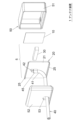
- FIG. 1 is an exploded perspective view of a patch antenna and an antenna device according to Embodiment 1 of the present invention, viewed from the front of the case of the antenna device;
- FIG. 2 is an exploded perspective view of the antenna device according to Embodiment 1 as seen from the rear of the case;
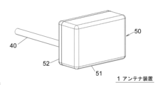
- FIG. FIG. 2 is a perspective view of the antenna device of Embodiment 1 as viewed from the front of the case;
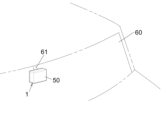
- 1 is a perspective view showing an antenna device arranged inside a windshield of a vehicle body according to the first embodiment;
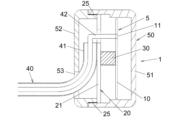
- FIG. FIG. 2 is a side sectional view of the antenna device according to Embodiment 1;
- 1 is a front view of a patch antenna according to Embodiment 1;
- FIG. 2 is a side view of the patch antenna according to Embodiment 1.
- FIG. 2 is a plan view of the patch antenna according to Embodiment 1.
- FIG. FIG. 2 is a diagram of directivity characteristics in the horizontal plane of the patch antenna according to Embodiment 1; 1 is a perspective view of a patch antenna having patch elements and a planar ground conductor substrate without conductor metal extensions; FIG. The perspective view of the patch antenna which added the conductor metal extension part to the planar ground conductor board
- FIG. 9B is a directional characteristic diagram in a horizontal plane showing the case of FIG. 9A by a dotted line and the case of FIG.
- a conductive metal extension is added to a planar ground conductor substrate (base), and patch elements are opposed to each other with dielectric spacers interposed therebetween, wherein the dielectric spacers control the resonance of the patch elements.
- Fig. 10 is a side view when in the position of the midpoint between the directional ends; A patch antenna in which a conductor metal extension is added to a planar ground conductor substrate (base), and a patch element is opposed to the patch element via a dielectric spacer, and the dielectric spacer is arranged at the end of the patch element in the resonance direction. Side view if installed.
- FIG. 10B is a horizontal plane directivity diagram showing the case of FIG.
- FIG. 10A by a solid line and the case of FIG. 10B by a dotted line;
- a patch antenna in which a conductor metal extension is added to a planar ground conductor substrate (base) and patch elements are opposed to each other via a dielectric spacer, wherein the dielectric spacer is between the ends of the patch element in the resonance direction.
- the side view at the position of the midpoint that is, the offset from the midpoint is 0 mm.
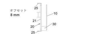
- FIG. 4 is a side view when the dielectric spacer is arranged at a position offset by 8 mm from the midpoint between the ends of the patch element in the resonance direction; 4 is a graph showing the relationship between the spacer offset position (mm) and the average gain (average Gain) [dBi] in the horizontal plane.
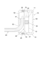
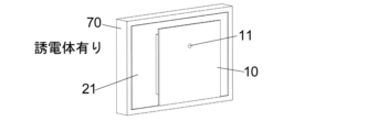
- FIG. 4 is a side cross-sectional view of the antenna device according to Embodiment 2; 1 is a perspective view of a patch antenna having patch elements and a planar ground conductor substrate without dielectric extensions; FIG. FIG. 2 is a perspective view of a patch antenna in which a planar ground conductor substrate is provided with a dielectric extension.
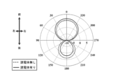
- FIG. 13B is a horizontal plane directivity diagram showing the case of FIG. 13A by a dotted line and the case of FIG. 13B by a solid line; A side view of an upper half of an antenna device for explaining a modification of the present invention.
- the antenna device 1 includes a patch antenna 5 , a dielectric spacer 30 , a coaxial cable 40 as a feeder line, and a radio wave transparent resin case 50 .
- the patch antenna 5 is composed of a patch element 10, which is a conductive metal plate, which is a radiation element, and a ground conductor 20 facing the patch element 10 at a predetermined interval.
- the ground conductor 20 faces the patch element 10 with a predetermined space therebetween via the spacer 30 .
- the patch antenna 5 will be described as an antenna for vertically polarized waves.
- Patch element 10 has an electrical length that corresponds to approximately one-half wavelength at the operating frequency.
- the shape of the patch element 10 is not limited to the square shown in FIGS. 1 and 2, and may be circular or the like.
- the ground conductor 20 has a ground conductor substrate 21 as a base of the ground conductor 20 facing in parallel with the patch element 10 and a conductor metal extension 25 provided at the end of the ground conductor substrate 21 .
- the ground conductor substrate 21 has, for example, double-sided conductive metal films electrically connected to each other, and the ends of the ground conductor substrate 21 (specifically, both sides of the ground conductor substrate 21 along the resonance direction of the patch element 10) is provided with a conductive metal extension 25 .
- the conductor metal extension 25 is electrically connected to the conductor metal film of the ground conductor substrate 21 .
- the conductor metal extension 25 is fixed to the end of the ground conductor substrate 21 as a separate component, or formed integrally with the ground conductor substrate 21 .
- the conductor metal film of the ground conductor substrate 21 should be present at least on the side facing the patch element 10 .
- the area of the conductor metal film of the ground conductor substrate 21 facing the patch element 10 is larger than the area of the patch element 10 facing.
- the dimension of the conductor metal film of the ground conductor substrate 21 viewed in the resonance direction of the patch element 10 is set longer than that of the patch element 10 .
- the conductor metal extension 25 is plate-shaped and extends from the end of the ground conductor substrate 21 in the direction opposite to the side where the patch element 10 is arranged. In the illustrated case, the conductor metal extension 25 is provided perpendicular to the ground conductor substrate 21 . Other cases than those shown in the drawings will be described as modified examples to be described later.
- the ground conductor substrate 21 may be a substrate made of a conductor metal plate itself instead of a double-sided conductor substrate.
- the spacer 30 is an insulating dielectric such as ABS resin, and has a prism shape, for example.
- the spacer 30 maintains a predetermined gap between the patch element 10 and the ground conductor substrate 21 due to its thickness, and integrally holds the two in a parallel or substantially parallel state.
- the spacer 30 integrally holds the patch element 10 and the ground conductor substrate 21 by using an adhesive means as necessary.
- a space between the patch element 10 and the ground conductor substrate 21 where the spacer 30 is not present is hollow.
- the area of the contact surface of the spacer 30 that contacts the patch element 10 and the ground conductor substrate 21 is set sufficiently smaller than the areas of the patch element 10 and the ground conductor substrate 21 in order to reduce the dielectric loss caused by the spacer 30. be.
- the outer conductor 41 of the coaxial cable 40 as the feeder line is electrically connected to the conductor metal film of the ground conductor substrate 21 via the holding metal fittings 45 (see FIG. 2).
- a central conductor 42 of the coaxial cable 40 passes through the ground conductor substrate 21 .
- the central conductor 42 of the coaxial cable 40 may pass through the conductor metal film of the ground conductor substrate 21 without contact.
- a central conductor 42 passing through the ground conductor substrate 21 is electrically connected to the patch element 10 at a feed point 11, which will be described later.
- the outer conductor 41 of the coaxial cable 40 is electrically connected to the side of the ground conductor substrate 21 opposite to the patch element 10 side.
- a central conductor 42 of the coaxial cable 41 is exposed to the patch element 10 side of the ground conductor substrate 21 through a through hole provided in the ground conductor substrate 21 . Exposed center conductor 42 is electrically connected to patch element 10 .
- the resin case 50 has a front side case portion (first case portion) 51 and a rear side case portion (second case portion) 52 .
- the front case part 51 and the rear case part 52 have, for example, a structure in which they are fitted together. Form. At least the front case portion 51, which has a portion facing the patch element 10, is radio wave transparent.
- the coaxial cable 40 is drawn into the internal space of the case 50 through the through hole 53 of the rear side case portion 52 .
- the patch antenna 5 and the through hole 53 ( 2) accommodates a portion of the coaxial cable 40 that is led through.
- the antenna device 1 shown in FIG. 3A is held by a support member 61 on the inner upper portion of the windshield 60 of the vehicle body as shown in FIG. 3B.
- the antenna device 1 functions as an in-vehicle antenna device.
- the antenna device 1 shown in FIG. 3B is held by the vehicle body 1 so that the radiation directivity of the patch element 10 of the patch antenna 5 housed in the resin case 50 is in the forward direction (traveling direction) of the vehicle body 1 .
- the patch antenna 5 housed in the internal space of the resin case 50 is arranged with a gap between the patch element 10 and the front case 51 .
- the patch element 10 is connected to the spacer 30 at a substantially intermediate position on the side opposite to the front case 51 side.
- the ground conductor substrate 21 is connected to the spacer 30 at a substantially intermediate position on the patch element 10 side. In this manner, the spacer 30 is held at a substantially intermediate position between the patch element 10 and the ground conductor substrate 21 with a predetermined gap therebetween.
- the outer conductor 41 of the coaxial cable 40 drawn into the inner space of the case 50 through the through-hole 53 of the rear-side case 52 extends from the bottom surface of the case 50 shown in FIG. Electrical connection is made at a position where the height (in FIGS. 4 and 5, the height direction is the vertical direction of the paper surface) is substantially the same as the height of the spacer 30 .
- a central conductor 42 of the coaxial cable 40 is exposed to the patch element 10 side from the through hole above the ground conductor substrate 42 shown in FIG. 4 and electrically connected to the feeding point 11 of the patch element 10 .
- the patch antenna 5 can be held with respect to the case 50 by sandwiching the conductor metal extension 25 between the front case 51 and the rear case 52 at the mating portion.
- FIG. 5 is a front view when the patch antenna 5 is viewed from the front side.
- the central conductor 42 of the coaxial cable 40 is electrically connected to the feeding point 11 provided on the patch element 10 . Electric waves are radiated from the patch element 10 by supplying electricity to the feeding point via the coaxial cable 40 .
- the size of the patch element 10 and the ground conductor substrate 21 is the width direction of the patch element 10 (horizontal direction of the paper surface) when viewed from the front (from the front side of the paper surface of FIG. 5).
- the size is smaller than the size of the ground conductor substrate 21, and the size in the vertical direction (the vertical direction of the paper surface) is approximately the same size.
- the patch element 10 is arranged substantially in the center of the ground conductor substrate 21 .
- the conductor metal extensions 25 provided at both ends of the ground conductor substrate 21 are provided in the vertical direction (the vertical direction of the paper surface) having substantially the same size in relation to the arrangement of the patch element 10 .
- the conductor metal extensions 25 are provided so as to extend in the opposite direction to the patch element 10 at both ends of the vertical ground conductor substrate 21 having approximately the same size as the patch element 10 . ing. Further, as shown in FIGS. 5 and 7, the conductor metal extension 25 is provided over substantially the entire length of the ground conductor substrate 21 (ground conductor 20) in the width direction (horizontal direction of the paper surface) shown in FIG. It is
- FIG. 8 is a diagram showing directivity characteristics in the horizontal plane when power is supplied from the coaxial cable 40 to the patch element 10 and vertically polarized radio waves are radiated from the patch element 10 in the antenna device 1 of Embodiment 1.
- FIG. 8 As is clear from the directivity characteristics in the horizontal plane in FIG. 8, good unidirectional directivity can be achieved without increasing the area of the ground conductor substrate 21 serving as the base of the ground conductor. The reason for this will be explained in the following FIGS. 9A-9C, 10A-10C and 11A-11C.
- FIG. 9A is a perspective view of a patch antenna having a patch element 10 and a planar ground conductor substrate 21 without conductor metal extensions
- FIG. 2 is a perspective view of a patch antenna in which a ground conductor 20 having a conductor metal extension 25 is opposed to the ground conductor 20 via a spacer 30.
- the gain of the patch element 10 in the forward direction is increased, the gain of the patch element 10 in the rearward direction (the direction toward the ground plane 20 side) is decreased, and the unidirectional directivity is improved.
- the conductor metal extension 25 is provided at the end of the planar ground conductor substrate 21 in the current direction, so that the electrical path of the ground conductor 20 in the current direction of the patch element 10 is reduced. This is because the length is extended and becomes sufficiently larger than half the wavelength of the operating frequency, and this changes the current distribution of the patch element, suppresses radiation from the ground conductor 20, and makes it possible to improve unidirectional directivity. become.
- FIG. 10A shows the patch antenna 5 of the first embodiment in which a conductor metal extension 25 is provided on a ground conductor substrate 21 as a planar ground conductor (base part), and patch elements 10 are opposed to each other with spacers 30 interposed therebetween.
- 10B is a similar patch antenna, but the spacer 30 is located at the end of the patch element 10 in the resonance direction. , in other words, it is a side view in the case of being arranged at the end in the current direction.
- the main polarization is vertical polarization
- the end of the patch element 10 in the resonance direction is the end in the vertical direction of the patch element 10 shown in the figure.
- the spacer 30 is positioned approximately midway between both ends of the patch element 10 in the resonance direction in FIG.
- the directivity in the horizontal plane is improved over the configuration of FIG. 10B located at .
- the reduction in dielectric loss improves the gain in all directions in the horizontal plane and improves the unidirectional directivity.
- the spacer 30 is positioned at the end of the patch element 10 in the resonance direction where the electric field strength is high, so the dielectric loss due to the spacer 30 increases, whereas the configuration of FIG. This is because, in this configuration, the spacer 30 is located substantially midway between the two end portions of the patch element 10 having the minimum electric field strength in the resonance direction, so the dielectric loss caused by the spacer 30 is reduced.
- FIGS. 11A to 11C changes in the forward average gain [dBi] of the patch element 10 depending on the position of the spacer 30 will be considered.
- FIGS. 11A and 11B show a patch antenna 5 in which a conductor metal extension 25 is provided on a ground conductor substrate 21 (base portion) and patch elements 10 are opposed to each other with spacers 30 interposed therebetween.
- FIG. 11A is a side view when the spacer 30 is arranged at a substantially middle position between both ends of the patch element 10 in the resonance direction, that is, at a position where the offset amount from the middle position is 0 mm, and FIG. FIG.
- FIG. 10 is a side view when the spacer 30 is arranged at a position offset by 8 mm from a substantially middle position between the ends of the patch element in the resonance direction.
- the average gain decreases as the amount of offset of the position of the spacer 30 increases from 0 mm.
- the dielectric loss caused by the spacer 30 is minimized at the spacer position where the spacer 30 is offset 0 mm.
- the directivity is as shown in the directivity diagram of FIG.
- good unidirectional directivity can be achieved without increasing the area of the ground conductor substrate 21, which serves as the base of the ground conductor.
- the antenna device 1 When the antenna device 1 is mounted on an automobile, the antenna device 1 is held by a support member 61 on the inner upper portion of the windshield 60 of the vehicle body, as shown in FIG. 3B, for example.
- the resonance direction having an electrical length corresponding to about 1/2 wavelength at the operating frequency of the patch element 10 is the vertical direction perpendicular to the horizontal plane.
- the main polarized waves of the patch antenna 5 of the antenna device 1 become vertically polarized waves, and by supplying predetermined high-frequency power from the coaxial cable 40 to the patch element 10, the vertically polarized radio waves are substantially unidirectionally polarized. (in the forward direction of patch element 10).
- the operating frequency of the patch antenna 5 is set to approximately 5.9 GHz.
- the vertical inner dimension of the resin case 50 is about 20 mm, and the distance between the patch element 10 and the ground conductor substrate 21 is several mm or less.
- the ground conductor 20 is electrically connected to a ground conductor substrate 21 as a conductor base facing the patch element 10 of the conductor plate and extends to the side opposite to the patch element 10 side.
- the electrical length of the ground conductor 20 can be increased without increasing the area of the conductor base parallel to the patch element 10, thus increasing the area of the conductor base.
- the directivity can be improved by suppressing the radiation toward the ground plane and increasing the gain in the forward direction of the patch element.
- miniaturization in the plane parallel to the patch element 10 can be achieved.
- the dielectric spacer 30 interposed between the patch element 10 and the ground conductor substrate 21 to integrate them has a smaller facing area than the patch element 10 and the ground conductor substrate 21, and the spacer 30 is located away from the end of the patch element 10 in the resonance direction where the strong electric field is generated, the dielectric loss due to the placement of the spacer 30 can be reduced.
- the patch antenna 5 is housed in a case 50 having a radio wave transparent portion, and the case 50 is supported inside the windshield of the vehicle body so that the patch antenna 5 is for vertically polarized waves.
- the case 50 has a combined structure of a front side case portion (first case portion) 51 and a rear side case portion (second case portion), and the conductor metal extension portion 25 integrated with the ground conductor substrate 21 is attached to the front case portion.
- the patch antenna 5 can be held in the case 50 by sandwiching it between the portion 51 and the rear side case portion 52, and the structure can be simplified.
- a dielectric extension 70 is provided on the ground conductor 20 in addition to the configuration of the first embodiment. Specifically, the dielectric extension 70 is provided over the ground conductor substrate 21 and the conductor metal extension 25 as a conductor base.
- the dielectric extension 70 is preferably made of a dielectric material having a dielectric constant substantially higher than that of the resin case 50 . Other configurations are the same as those of the first embodiment.
- the dielectric extension 70 may be arranged outside or inside the ground conductor substrate 21 and the conductor metal extension 25 .
- FIG. 13A is a perspective view of a basic patch antenna having a patch element 10 and a planar ground conductor substrate 21 (without dielectric extension), and FIG. FIG. 4 is a perspective view of a patch antenna with an extension 70 added; Even if the area of the planar ground conductor substrate 21 facing the patch element 10 in parallel with the front is the same in FIGS. 13A and 13B, in FIG.
- the dielectric extension 70 so as to surround the end of the planar ground conductor substrate 21, the directivity in the horizontal plane is improved.
- the gain in the forward direction toward the patch element 10 increases and the gain in the backward direction toward the ground plane 20 decreases, so that unidirectional directivity is maintained satisfactorily.
- the dielectric extension part 70 is provided at the end of the flat ground conductor substrate 21 in the current direction, so that the ground conductor substrate 21 in the current direction of the patch element 10 is electrically This is because the path length is extended to be much larger than half the wavelength of the operating frequency. Due to this effect, in the antenna device 1A, the current distribution of the patch element 10 is changed, the radiation from the ground conductor 20 is suppressed, and the unidirectional directivity can be maintained.
- Embodiment 1 the configuration in which the conductor metal extension 25 extends from the end of the ground conductor substrate 21 to the side opposite to the patch element side perpendicularly to the surface of the ground conductor substrate 21 is illustrated.
- the inclination angle of the conductor metal extension 25 is not limited to vertical (except for the orientation parallel to the ground conductor substrate 21).
- the inclination angle of the conductor metal extension 25 with respect to the ground conductor substrate 21 when perpendicular to the surface of the ground conductor substrate 21 on the side opposite to the patch element side is -90°, and the angle parallel to the surface of the ground conductor substrate 21 is 0°, and the inclination angle of the conductor metal extension 25 with respect to the ground conductor substrate 21 when it is perpendicular to the surface of the ground conductor substrate 21 on the patch element side is defined as +90°, the inclination angle range ⁇ ( ⁇ 90° ⁇ 0°) or a tilt angle range ⁇ (0° ⁇ +90°).
- the tilt angle range ⁇ is preferable because it has less influence on the patch element 10 .
- the extension portion 70 may be arranged at the end portion of the ground conductor substrate 21 . It is preferable to dispose the dielectric extension 70 away from the end of the patch element 10 in the resonance direction in order to reduce the dielectric loss.
- ground conductor 20 instead of constructing the ground conductor 20 with a ground conductor substrate 21 as a base and conductor metal extensions 25 provided at the ends of the ground conductor substrate 21, a base and extensions bent with respect to the base are provided. It may be integrally formed from a conductive metal sheet. Also, the ground conductor 20 is not limited to a rectangular shape, and may be any shape as long as the area facing the patch element is larger than the patch element.
Landscapes
- Engineering & Computer Science (AREA)
- Remote Sensing (AREA)
- Waveguide Aerials (AREA)
Priority Applications (4)
| Application Number | Priority Date | Filing Date | Title |
|---|---|---|---|
| US18/723,468 US20250055181A1 (en) | 2021-12-24 | 2022-12-05 | Patch antenna and antenna device |
| CN202280085001.3A CN118435462A (zh) | 2021-12-24 | 2022-12-05 | 贴片天线以及天线装置 |
| JP2023569264A JPWO2023120146A1 (https=) | 2021-12-24 | 2022-12-05 | |
| DE112022005103.5T DE112022005103T5 (de) | 2021-12-24 | 2022-12-05 | Patch-Antenne und Antennenvorrichtung |
Applications Claiming Priority (2)
| Application Number | Priority Date | Filing Date | Title |
|---|---|---|---|
| JP2021211716 | 2021-12-24 | ||
| JP2021-211716 | 2021-12-24 |
Publications (1)
| Publication Number | Publication Date |
|---|---|
| WO2023120146A1 true WO2023120146A1 (ja) | 2023-06-29 |
Family
ID=86902216
Family Applications (1)
| Application Number | Title | Priority Date | Filing Date |
|---|---|---|---|
| PCT/JP2022/044799 Ceased WO2023120146A1 (ja) | 2021-12-24 | 2022-12-05 | パッチアンテナ及びアンテナ装置 |
Country Status (5)
| Country | Link |
|---|---|
| US (1) | US20250055181A1 (https=) |
| JP (1) | JPWO2023120146A1 (https=) |
| CN (1) | CN118435462A (https=) |
| DE (1) | DE112022005103T5 (https=) |
| WO (1) | WO2023120146A1 (https=) |
Citations (3)
| Publication number | Priority date | Publication date | Assignee | Title |
|---|---|---|---|---|
| JP2007013857A (ja) * | 2005-07-04 | 2007-01-18 | Alps Electric Co Ltd | 平面アンテナ装置 |
| WO2018074056A1 (ja) * | 2016-10-21 | 2018-04-26 | 株式会社デンソー | アンテナ装置 |
| JP2019075644A (ja) * | 2017-10-13 | 2019-05-16 | 株式会社ヨコオ | パッチアンテナおよび車載用アンテナ装置 |
Family Cites Families (4)
| Publication number | Priority date | Publication date | Assignee | Title |
|---|---|---|---|---|
| JPH0547714Y2 (https=) | 1987-12-29 | 1993-12-16 | ||
| JPH02126413U (https=) * | 1989-03-28 | 1990-10-18 | ||
| CA2629035A1 (en) * | 2008-03-27 | 2009-09-27 | Her Majesty The Queen In Right Of Canada, As Represented By The Minister Of Industry, Through The Communications Research Centre Canada | Waveguide filter with broad stopband based on sugstrate integrated waveguide scheme |
| DE102018200758A1 (de) * | 2018-01-18 | 2019-07-18 | Robert Bosch Gmbh | Antennenelement und Antennenarray |
-
2022
- 2022-12-05 US US18/723,468 patent/US20250055181A1/en active Pending
- 2022-12-05 JP JP2023569264A patent/JPWO2023120146A1/ja active Pending
- 2022-12-05 WO PCT/JP2022/044799 patent/WO2023120146A1/ja not_active Ceased
- 2022-12-05 DE DE112022005103.5T patent/DE112022005103T5/de active Pending
- 2022-12-05 CN CN202280085001.3A patent/CN118435462A/zh active Pending
Patent Citations (3)
| Publication number | Priority date | Publication date | Assignee | Title |
|---|---|---|---|---|
| JP2007013857A (ja) * | 2005-07-04 | 2007-01-18 | Alps Electric Co Ltd | 平面アンテナ装置 |
| WO2018074056A1 (ja) * | 2016-10-21 | 2018-04-26 | 株式会社デンソー | アンテナ装置 |
| JP2019075644A (ja) * | 2017-10-13 | 2019-05-16 | 株式会社ヨコオ | パッチアンテナおよび車載用アンテナ装置 |
Also Published As
| Publication number | Publication date |
|---|---|
| CN118435462A (zh) | 2024-08-02 |
| JPWO2023120146A1 (https=) | 2023-06-29 |
| DE112022005103T5 (de) | 2024-08-29 |
| US20250055181A1 (en) | 2025-02-13 |
Similar Documents
| Publication | Publication Date | Title |
|---|---|---|
| JP6964601B2 (ja) | アンテナ装置 | |
| JP3960701B2 (ja) | グリッドアレイアンテナ | |
| US11177578B2 (en) | Antenna device for vehicle | |
| JPH08222940A (ja) | アンテナ装置 | |
| US8125392B2 (en) | Antenna and electronic apparatus | |
| CN101548433A (zh) | 扇形天线 | |
| JP2008141765A (ja) | 高次共振モードを用いるビームチルトパッチアンテナ | |
| US11201409B2 (en) | Patch antenna and antenna device | |
| CN110574230B (zh) | 车载用天线装置 | |
| GB2286926A (en) | Microstrip antenna shaped about an axis | |
| CN116636088A (zh) | 贴片天线及车载用天线装置 | |
| US12294144B2 (en) | Antenna device for vehicle | |
| JP2005303946A (ja) | 自動車用高周波ガラスアンテナ | |
| JP2001156544A (ja) | アンテナ装置 | |
| JP4516246B2 (ja) | アンテナ | |
| JP5246115B2 (ja) | アンテナ及びアンテナを備えた電子機器 | |
| WO2023120146A1 (ja) | パッチアンテナ及びアンテナ装置 | |
| WO2024225038A1 (ja) | アンテナ装置、アンテナならびに車両 | |
| JP7781855B2 (ja) | アンテナ装置 | |
| JP3344415B2 (ja) | アンテナ装置 | |
| JPH07111418A (ja) | 偏波ダイバーシティ用平面アンテナ | |
| JP2645700B2 (ja) | 2周波共用コーナアンテナ装置 | |
| US20240030624A1 (en) | Antenna device | |
| JPH073928B2 (ja) | アンテナ装置 | |
| JP3846663B2 (ja) | 開口形アンテナおよびアレイアンテナ |
Legal Events
| Date | Code | Title | Description |
|---|---|---|---|
| 121 | Ep: the epo has been informed by wipo that ep was designated in this application |
Ref document number: 22910860 Country of ref document: EP Kind code of ref document: A1 |
|
| WWE | Wipo information: entry into national phase |
Ref document number: 2023569264 Country of ref document: JP |
|
| WWE | Wipo information: entry into national phase |
Ref document number: 202280085001.3 Country of ref document: CN Ref document number: 112022005103 Country of ref document: DE |
|
| WWE | Wipo information: entry into national phase |
Ref document number: 18723468 Country of ref document: US |
|
| 122 | Ep: pct application non-entry in european phase |
Ref document number: 22910860 Country of ref document: EP Kind code of ref document: A1 |