WO2023120146A1 - Patch antenna and antenna device - Google Patents
Patch antenna and antenna device Download PDFInfo
- Publication number
- WO2023120146A1 WO2023120146A1 PCT/JP2022/044799 JP2022044799W WO2023120146A1 WO 2023120146 A1 WO2023120146 A1 WO 2023120146A1 JP 2022044799 W JP2022044799 W JP 2022044799W WO 2023120146 A1 WO2023120146 A1 WO 2023120146A1
- Authority
- WO
- WIPO (PCT)
- Prior art keywords
- patch
- conductor
- ground conductor
- patch element
- extension
- Prior art date
Links
- 239000004020 conductor Substances 0.000 claims abstract description 214
- 125000006850 spacer group Chemical group 0.000 claims description 49
- 230000010287 polarization Effects 0.000 claims description 4
- 239000000758 substrate Substances 0.000 abstract description 85
- 239000002184 metal Substances 0.000 abstract description 51
- 230000005855 radiation Effects 0.000 description 10
- 239000011347 resin Substances 0.000 description 7
- 229920005989 resin Polymers 0.000 description 7
- 238000010586 diagram Methods 0.000 description 6
- 230000005684 electric field Effects 0.000 description 6
- 230000000694 effects Effects 0.000 description 5
- 238000004891 communication Methods 0.000 description 4
- 238000000034 method Methods 0.000 description 4
- 230000003071 parasitic effect Effects 0.000 description 4
- 230000004048 modification Effects 0.000 description 3
- 238000012986 modification Methods 0.000 description 3
- 230000002457 bidirectional effect Effects 0.000 description 2
- 239000000470 constituent Substances 0.000 description 2
- 230000007423 decrease Effects 0.000 description 2
- 230000008569 process Effects 0.000 description 2
- 229920000122 acrylonitrile butadiene styrene Polymers 0.000 description 1
- 239000000853 adhesive Substances 0.000 description 1
- 230000001070 adhesive effect Effects 0.000 description 1
- 238000006243 chemical reaction Methods 0.000 description 1
- 230000003247 decreasing effect Effects 0.000 description 1
- 239000003989 dielectric material Substances 0.000 description 1
- 230000005611 electricity Effects 0.000 description 1
- 239000011796 hollow space material Substances 0.000 description 1
- 230000006872 improvement Effects 0.000 description 1
- 230000013011 mating Effects 0.000 description 1
- 230000009467 reduction Effects 0.000 description 1
Images


Classifications
-
- H—ELECTRICITY
- H01—ELECTRIC ELEMENTS
- H01Q—ANTENNAS, i.e. RADIO AERIALS
- H01Q1/00—Details of, or arrangements associated with, antennas
- H01Q1/12—Supports; Mounting means
- H01Q1/22—Supports; Mounting means by structural association with other equipment or articles
-
- H—ELECTRICITY
- H01—ELECTRIC ELEMENTS
- H01Q—ANTENNAS, i.e. RADIO AERIALS
- H01Q13/00—Waveguide horns or mouths; Slot antennas; Leaky-waveguide antennas; Equivalent structures causing radiation along the transmission path of a guided wave
- H01Q13/08—Radiating ends of two-conductor microwave transmission lines, e.g. of coaxial lines, of microstrip lines
Definitions
- the present invention relates to a patch antenna having a patch element as an element for transmitting and receiving radio waves and an antenna apparatus having the same.
- Patch antennas using patch elements are widely known as small and thin unidirectional antennas, and are used for various purposes including satellite communications.
- a patch antenna is an antenna having radiation directivity in a direction perpendicular to the radiation surface of the patch element and opposite to the direction of the opposing ground conductor. This unidirectional directivity is premised on the fact that the ground conductor has a sufficiently large area compared to the patch element.
- the patch element that radiates linearly polarized waves is square or circular
- a standing wave current is generated in the longitudinal direction of the radiation surface of the patch element, for example, in the linear direction connecting the feed point and the center of the patch element.
- a strong electric field region is generated in the gap between the end of the patch element and the ground conductor in the current direction.
- the patch element emits radio waves. Radio waves are radiated in the opposite direction as well.
- the patch antenna requires a sufficiently wide area of the ground conductor with respect to the patch element in order to have the original unidirectional directivity due to its principle of operation.
- Patent Document 1 has been proposed by the present applicant as an antenna device using a patch element.
- the radiation pattern changes from unidirectional directivity to bidirectional directivity. deteriorated, which is not desirable. Also, when a parasitic patch element is mounted, a region for mounting the parasitic patch element is required.
- One example of the purpose of the present invention is to enable improvement of unidirectional directivity.
- a first aspect of the present invention is a patch antenna.
- This patch antenna includes a patch element of a conductive plate, A ground conductor having a conductor base facing the patch element and a conductor extension or dielectric extension is provided.
- the conductor extension may be electrically connected to the end of the conductor base and may be provided perpendicularly or inclined to a plane formed by the conductor base.
- the conductor extension is provided on the opposite side of the patch element from the plane formed by the conductor base so as to be perpendicular or inclined.
- the dielectric extension may be provided on one or both of the conductor base and the conductor extension.
- a dielectric spacer is interposed between the patch element and the conductor base, the dielectric spacer has a smaller facing area than the patch element and the conductor base, and the patch without the dielectric spacer. There may be a hollow space between the element and the conductor base.
- the dielectric spacer is preferably arranged at a position spaced apart from the end of the patch element in the resonance direction.
- a center conductor of a coaxial cable may be connected to the patch element, and an outer conductor of the coaxial cable may be connected to the ground conductor.
- a second aspect of the present invention is an antenna device.
- This antenna device accommodates the patch antenna in a case having a radio wave transparent portion.
- the patch antenna be supported by the vehicle body so that the main polarized wave is vertical polarized wave.
- the case has a combined structure of a first case portion and a second case portion, and the conductor extension portion or the dielectric extension portion is sandwiched between the first case portion and the second case portion.
- FIG. 1 is an exploded perspective view of a patch antenna and an antenna device according to Embodiment 1 of the present invention, viewed from the front of the case of the antenna device;
- FIG. 2 is an exploded perspective view of the antenna device according to Embodiment 1 as seen from the rear of the case;
- FIG. FIG. 2 is a perspective view of the antenna device of Embodiment 1 as viewed from the front of the case;
- 1 is a perspective view showing an antenna device arranged inside a windshield of a vehicle body according to the first embodiment;
- FIG. FIG. 2 is a side sectional view of the antenna device according to Embodiment 1;
- 1 is a front view of a patch antenna according to Embodiment 1;
- FIG. 2 is a side view of the patch antenna according to Embodiment 1.
- FIG. 2 is a plan view of the patch antenna according to Embodiment 1.
- FIG. FIG. 2 is a diagram of directivity characteristics in the horizontal plane of the patch antenna according to Embodiment 1; 1 is a perspective view of a patch antenna having patch elements and a planar ground conductor substrate without conductor metal extensions; FIG. The perspective view of the patch antenna which added the conductor metal extension part to the planar ground conductor board
- FIG. 9B is a directional characteristic diagram in a horizontal plane showing the case of FIG. 9A by a dotted line and the case of FIG.
- a conductive metal extension is added to a planar ground conductor substrate (base), and patch elements are opposed to each other with dielectric spacers interposed therebetween, wherein the dielectric spacers control the resonance of the patch elements.
- Fig. 10 is a side view when in the position of the midpoint between the directional ends; A patch antenna in which a conductor metal extension is added to a planar ground conductor substrate (base), and a patch element is opposed to the patch element via a dielectric spacer, and the dielectric spacer is arranged at the end of the patch element in the resonance direction. Side view if installed.
- FIG. 10B is a horizontal plane directivity diagram showing the case of FIG.
- FIG. 10A by a solid line and the case of FIG. 10B by a dotted line;
- a patch antenna in which a conductor metal extension is added to a planar ground conductor substrate (base) and patch elements are opposed to each other via a dielectric spacer, wherein the dielectric spacer is between the ends of the patch element in the resonance direction.
- the side view at the position of the midpoint that is, the offset from the midpoint is 0 mm.
- FIG. 4 is a side view when the dielectric spacer is arranged at a position offset by 8 mm from the midpoint between the ends of the patch element in the resonance direction; 4 is a graph showing the relationship between the spacer offset position (mm) and the average gain (average Gain) [dBi] in the horizontal plane.
- FIG. 4 is a side cross-sectional view of the antenna device according to Embodiment 2; 1 is a perspective view of a patch antenna having patch elements and a planar ground conductor substrate without dielectric extensions; FIG. FIG. 2 is a perspective view of a patch antenna in which a planar ground conductor substrate is provided with a dielectric extension.
- FIG. 13B is a horizontal plane directivity diagram showing the case of FIG. 13A by a dotted line and the case of FIG. 13B by a solid line; A side view of an upper half of an antenna device for explaining a modification of the present invention.
- the antenna device 1 includes a patch antenna 5 , a dielectric spacer 30 , a coaxial cable 40 as a feeder line, and a radio wave transparent resin case 50 .
- the patch antenna 5 is composed of a patch element 10, which is a conductive metal plate, which is a radiation element, and a ground conductor 20 facing the patch element 10 at a predetermined interval.
- the ground conductor 20 faces the patch element 10 with a predetermined space therebetween via the spacer 30 .
- the patch antenna 5 will be described as an antenna for vertically polarized waves.
- Patch element 10 has an electrical length that corresponds to approximately one-half wavelength at the operating frequency.
- the shape of the patch element 10 is not limited to the square shown in FIGS. 1 and 2, and may be circular or the like.
- the ground conductor 20 has a ground conductor substrate 21 as a base of the ground conductor 20 facing in parallel with the patch element 10 and a conductor metal extension 25 provided at the end of the ground conductor substrate 21 .
- the ground conductor substrate 21 has, for example, double-sided conductive metal films electrically connected to each other, and the ends of the ground conductor substrate 21 (specifically, both sides of the ground conductor substrate 21 along the resonance direction of the patch element 10) is provided with a conductive metal extension 25 .
- the conductor metal extension 25 is electrically connected to the conductor metal film of the ground conductor substrate 21 .
- the conductor metal extension 25 is fixed to the end of the ground conductor substrate 21 as a separate component, or formed integrally with the ground conductor substrate 21 .
- the conductor metal film of the ground conductor substrate 21 should be present at least on the side facing the patch element 10 .
- the area of the conductor metal film of the ground conductor substrate 21 facing the patch element 10 is larger than the area of the patch element 10 facing.
- the dimension of the conductor metal film of the ground conductor substrate 21 viewed in the resonance direction of the patch element 10 is set longer than that of the patch element 10 .
- the conductor metal extension 25 is plate-shaped and extends from the end of the ground conductor substrate 21 in the direction opposite to the side where the patch element 10 is arranged. In the illustrated case, the conductor metal extension 25 is provided perpendicular to the ground conductor substrate 21 . Other cases than those shown in the drawings will be described as modified examples to be described later.
- the ground conductor substrate 21 may be a substrate made of a conductor metal plate itself instead of a double-sided conductor substrate.
- the spacer 30 is an insulating dielectric such as ABS resin, and has a prism shape, for example.
- the spacer 30 maintains a predetermined gap between the patch element 10 and the ground conductor substrate 21 due to its thickness, and integrally holds the two in a parallel or substantially parallel state.
- the spacer 30 integrally holds the patch element 10 and the ground conductor substrate 21 by using an adhesive means as necessary.
- a space between the patch element 10 and the ground conductor substrate 21 where the spacer 30 is not present is hollow.
- the area of the contact surface of the spacer 30 that contacts the patch element 10 and the ground conductor substrate 21 is set sufficiently smaller than the areas of the patch element 10 and the ground conductor substrate 21 in order to reduce the dielectric loss caused by the spacer 30. be.
- the outer conductor 41 of the coaxial cable 40 as the feeder line is electrically connected to the conductor metal film of the ground conductor substrate 21 via the holding metal fittings 45 (see FIG. 2).
- a central conductor 42 of the coaxial cable 40 passes through the ground conductor substrate 21 .
- the central conductor 42 of the coaxial cable 40 may pass through the conductor metal film of the ground conductor substrate 21 without contact.
- a central conductor 42 passing through the ground conductor substrate 21 is electrically connected to the patch element 10 at a feed point 11, which will be described later.
- the outer conductor 41 of the coaxial cable 40 is electrically connected to the side of the ground conductor substrate 21 opposite to the patch element 10 side.
- a central conductor 42 of the coaxial cable 41 is exposed to the patch element 10 side of the ground conductor substrate 21 through a through hole provided in the ground conductor substrate 21 . Exposed center conductor 42 is electrically connected to patch element 10 .
- the resin case 50 has a front side case portion (first case portion) 51 and a rear side case portion (second case portion) 52 .
- the front case part 51 and the rear case part 52 have, for example, a structure in which they are fitted together. Form. At least the front case portion 51, which has a portion facing the patch element 10, is radio wave transparent.
- the coaxial cable 40 is drawn into the internal space of the case 50 through the through hole 53 of the rear side case portion 52 .
- the patch antenna 5 and the through hole 53 ( 2) accommodates a portion of the coaxial cable 40 that is led through.
- the antenna device 1 shown in FIG. 3A is held by a support member 61 on the inner upper portion of the windshield 60 of the vehicle body as shown in FIG. 3B.
- the antenna device 1 functions as an in-vehicle antenna device.
- the antenna device 1 shown in FIG. 3B is held by the vehicle body 1 so that the radiation directivity of the patch element 10 of the patch antenna 5 housed in the resin case 50 is in the forward direction (traveling direction) of the vehicle body 1 .
- the patch antenna 5 housed in the internal space of the resin case 50 is arranged with a gap between the patch element 10 and the front case 51 .
- the patch element 10 is connected to the spacer 30 at a substantially intermediate position on the side opposite to the front case 51 side.
- the ground conductor substrate 21 is connected to the spacer 30 at a substantially intermediate position on the patch element 10 side. In this manner, the spacer 30 is held at a substantially intermediate position between the patch element 10 and the ground conductor substrate 21 with a predetermined gap therebetween.
- the outer conductor 41 of the coaxial cable 40 drawn into the inner space of the case 50 through the through-hole 53 of the rear-side case 52 extends from the bottom surface of the case 50 shown in FIG. Electrical connection is made at a position where the height (in FIGS. 4 and 5, the height direction is the vertical direction of the paper surface) is substantially the same as the height of the spacer 30 .
- a central conductor 42 of the coaxial cable 40 is exposed to the patch element 10 side from the through hole above the ground conductor substrate 42 shown in FIG. 4 and electrically connected to the feeding point 11 of the patch element 10 .
- the patch antenna 5 can be held with respect to the case 50 by sandwiching the conductor metal extension 25 between the front case 51 and the rear case 52 at the mating portion.
- FIG. 5 is a front view when the patch antenna 5 is viewed from the front side.
- the central conductor 42 of the coaxial cable 40 is electrically connected to the feeding point 11 provided on the patch element 10 . Electric waves are radiated from the patch element 10 by supplying electricity to the feeding point via the coaxial cable 40 .
- the size of the patch element 10 and the ground conductor substrate 21 is the width direction of the patch element 10 (horizontal direction of the paper surface) when viewed from the front (from the front side of the paper surface of FIG. 5).
- the size is smaller than the size of the ground conductor substrate 21, and the size in the vertical direction (the vertical direction of the paper surface) is approximately the same size.
- the patch element 10 is arranged substantially in the center of the ground conductor substrate 21 .
- the conductor metal extensions 25 provided at both ends of the ground conductor substrate 21 are provided in the vertical direction (the vertical direction of the paper surface) having substantially the same size in relation to the arrangement of the patch element 10 .
- the conductor metal extensions 25 are provided so as to extend in the opposite direction to the patch element 10 at both ends of the vertical ground conductor substrate 21 having approximately the same size as the patch element 10 . ing. Further, as shown in FIGS. 5 and 7, the conductor metal extension 25 is provided over substantially the entire length of the ground conductor substrate 21 (ground conductor 20) in the width direction (horizontal direction of the paper surface) shown in FIG. It is
- FIG. 8 is a diagram showing directivity characteristics in the horizontal plane when power is supplied from the coaxial cable 40 to the patch element 10 and vertically polarized radio waves are radiated from the patch element 10 in the antenna device 1 of Embodiment 1.
- FIG. 8 As is clear from the directivity characteristics in the horizontal plane in FIG. 8, good unidirectional directivity can be achieved without increasing the area of the ground conductor substrate 21 serving as the base of the ground conductor. The reason for this will be explained in the following FIGS. 9A-9C, 10A-10C and 11A-11C.
- FIG. 9A is a perspective view of a patch antenna having a patch element 10 and a planar ground conductor substrate 21 without conductor metal extensions
- FIG. 2 is a perspective view of a patch antenna in which a ground conductor 20 having a conductor metal extension 25 is opposed to the ground conductor 20 via a spacer 30.
- the gain of the patch element 10 in the forward direction is increased, the gain of the patch element 10 in the rearward direction (the direction toward the ground plane 20 side) is decreased, and the unidirectional directivity is improved.
- the conductor metal extension 25 is provided at the end of the planar ground conductor substrate 21 in the current direction, so that the electrical path of the ground conductor 20 in the current direction of the patch element 10 is reduced. This is because the length is extended and becomes sufficiently larger than half the wavelength of the operating frequency, and this changes the current distribution of the patch element, suppresses radiation from the ground conductor 20, and makes it possible to improve unidirectional directivity. become.
- FIG. 10A shows the patch antenna 5 of the first embodiment in which a conductor metal extension 25 is provided on a ground conductor substrate 21 as a planar ground conductor (base part), and patch elements 10 are opposed to each other with spacers 30 interposed therebetween.
- 10B is a similar patch antenna, but the spacer 30 is located at the end of the patch element 10 in the resonance direction. , in other words, it is a side view in the case of being arranged at the end in the current direction.
- the main polarization is vertical polarization
- the end of the patch element 10 in the resonance direction is the end in the vertical direction of the patch element 10 shown in the figure.
- the spacer 30 is positioned approximately midway between both ends of the patch element 10 in the resonance direction in FIG.
- the directivity in the horizontal plane is improved over the configuration of FIG. 10B located at .
- the reduction in dielectric loss improves the gain in all directions in the horizontal plane and improves the unidirectional directivity.
- the spacer 30 is positioned at the end of the patch element 10 in the resonance direction where the electric field strength is high, so the dielectric loss due to the spacer 30 increases, whereas the configuration of FIG. This is because, in this configuration, the spacer 30 is located substantially midway between the two end portions of the patch element 10 having the minimum electric field strength in the resonance direction, so the dielectric loss caused by the spacer 30 is reduced.
- FIGS. 11A to 11C changes in the forward average gain [dBi] of the patch element 10 depending on the position of the spacer 30 will be considered.
- FIGS. 11A and 11B show a patch antenna 5 in which a conductor metal extension 25 is provided on a ground conductor substrate 21 (base portion) and patch elements 10 are opposed to each other with spacers 30 interposed therebetween.
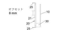
- FIG. 11A is a side view when the spacer 30 is arranged at a substantially middle position between both ends of the patch element 10 in the resonance direction, that is, at a position where the offset amount from the middle position is 0 mm, and FIG. FIG.
- FIG. 10 is a side view when the spacer 30 is arranged at a position offset by 8 mm from a substantially middle position between the ends of the patch element in the resonance direction.
- the average gain decreases as the amount of offset of the position of the spacer 30 increases from 0 mm.
- the dielectric loss caused by the spacer 30 is minimized at the spacer position where the spacer 30 is offset 0 mm.
- the directivity is as shown in the directivity diagram of FIG.
- good unidirectional directivity can be achieved without increasing the area of the ground conductor substrate 21, which serves as the base of the ground conductor.
- the antenna device 1 When the antenna device 1 is mounted on an automobile, the antenna device 1 is held by a support member 61 on the inner upper portion of the windshield 60 of the vehicle body, as shown in FIG. 3B, for example.
- the resonance direction having an electrical length corresponding to about 1/2 wavelength at the operating frequency of the patch element 10 is the vertical direction perpendicular to the horizontal plane.
- the main polarized waves of the patch antenna 5 of the antenna device 1 become vertically polarized waves, and by supplying predetermined high-frequency power from the coaxial cable 40 to the patch element 10, the vertically polarized radio waves are substantially unidirectionally polarized. (in the forward direction of patch element 10).
- the operating frequency of the patch antenna 5 is set to approximately 5.9 GHz.
- the vertical inner dimension of the resin case 50 is about 20 mm, and the distance between the patch element 10 and the ground conductor substrate 21 is several mm or less.
- the ground conductor 20 is electrically connected to a ground conductor substrate 21 as a conductor base facing the patch element 10 of the conductor plate and extends to the side opposite to the patch element 10 side.
- the electrical length of the ground conductor 20 can be increased without increasing the area of the conductor base parallel to the patch element 10, thus increasing the area of the conductor base.
- the directivity can be improved by suppressing the radiation toward the ground plane and increasing the gain in the forward direction of the patch element.
- miniaturization in the plane parallel to the patch element 10 can be achieved.
- the dielectric spacer 30 interposed between the patch element 10 and the ground conductor substrate 21 to integrate them has a smaller facing area than the patch element 10 and the ground conductor substrate 21, and the spacer 30 is located away from the end of the patch element 10 in the resonance direction where the strong electric field is generated, the dielectric loss due to the placement of the spacer 30 can be reduced.
- the patch antenna 5 is housed in a case 50 having a radio wave transparent portion, and the case 50 is supported inside the windshield of the vehicle body so that the patch antenna 5 is for vertically polarized waves.
- the case 50 has a combined structure of a front side case portion (first case portion) 51 and a rear side case portion (second case portion), and the conductor metal extension portion 25 integrated with the ground conductor substrate 21 is attached to the front case portion.
- the patch antenna 5 can be held in the case 50 by sandwiching it between the portion 51 and the rear side case portion 52, and the structure can be simplified.
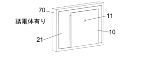
- a dielectric extension 70 is provided on the ground conductor 20 in addition to the configuration of the first embodiment. Specifically, the dielectric extension 70 is provided over the ground conductor substrate 21 and the conductor metal extension 25 as a conductor base.
- the dielectric extension 70 is preferably made of a dielectric material having a dielectric constant substantially higher than that of the resin case 50 . Other configurations are the same as those of the first embodiment.
- the dielectric extension 70 may be arranged outside or inside the ground conductor substrate 21 and the conductor metal extension 25 .
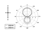
- FIG. 13A is a perspective view of a basic patch antenna having a patch element 10 and a planar ground conductor substrate 21 (without dielectric extension), and FIG. FIG. 4 is a perspective view of a patch antenna with an extension 70 added; Even if the area of the planar ground conductor substrate 21 facing the patch element 10 in parallel with the front is the same in FIGS. 13A and 13B, in FIG.
- the dielectric extension 70 so as to surround the end of the planar ground conductor substrate 21, the directivity in the horizontal plane is improved.
- the gain in the forward direction toward the patch element 10 increases and the gain in the backward direction toward the ground plane 20 decreases, so that unidirectional directivity is maintained satisfactorily.
- the dielectric extension part 70 is provided at the end of the flat ground conductor substrate 21 in the current direction, so that the ground conductor substrate 21 in the current direction of the patch element 10 is electrically This is because the path length is extended to be much larger than half the wavelength of the operating frequency. Due to this effect, in the antenna device 1A, the current distribution of the patch element 10 is changed, the radiation from the ground conductor 20 is suppressed, and the unidirectional directivity can be maintained.
- Embodiment 1 the configuration in which the conductor metal extension 25 extends from the end of the ground conductor substrate 21 to the side opposite to the patch element side perpendicularly to the surface of the ground conductor substrate 21 is illustrated.
- the inclination angle of the conductor metal extension 25 is not limited to vertical (except for the orientation parallel to the ground conductor substrate 21).
- the inclination angle of the conductor metal extension 25 with respect to the ground conductor substrate 21 when perpendicular to the surface of the ground conductor substrate 21 on the side opposite to the patch element side is -90°, and the angle parallel to the surface of the ground conductor substrate 21 is 0°, and the inclination angle of the conductor metal extension 25 with respect to the ground conductor substrate 21 when it is perpendicular to the surface of the ground conductor substrate 21 on the patch element side is defined as +90°, the inclination angle range ⁇ ( ⁇ 90° ⁇ 0°) or a tilt angle range ⁇ (0° ⁇ +90°).
- the tilt angle range ⁇ is preferable because it has less influence on the patch element 10 .
- the extension portion 70 may be arranged at the end portion of the ground conductor substrate 21 . It is preferable to dispose the dielectric extension 70 away from the end of the patch element 10 in the resonance direction in order to reduce the dielectric loss.
- ground conductor 20 instead of constructing the ground conductor 20 with a ground conductor substrate 21 as a base and conductor metal extensions 25 provided at the ends of the ground conductor substrate 21, a base and extensions bent with respect to the base are provided. It may be integrally formed from a conductive metal sheet. Also, the ground conductor 20 is not limited to a rectangular shape, and may be any shape as long as the area facing the patch element is larger than the patch element.
Abstract
Provided are a patch antenna and an antenna device that are capable of maintaining unidirectionality even if the area size of a ground conductor facing a patch element is restricted. A patch antenna 5 comprises: a patch element 10 of a conductor plate; and a ground conductor 20 that has a ground conductor substrate 21, which serves as a conductor base part facing the patch element 10, and has conductor metal extension parts 25. The conductor metal extension parts 25 are electrically connected to ends of the ground conductor substrate 21 and are arranged so as to be perpendicular or inclined to a plane formed by the ground conductor substrate 21.
Description
本発明は、電波を送受信するエレメントとしてパッチ素子を有するパッチアンテナ及びそれを具備するアンテナ装置に関する。
The present invention relates to a patch antenna having a patch element as an element for transmitting and receiving radio waves and an antenna apparatus having the same.
小型かつ薄型の単方向指向性アンテナとして、放射エレメントであるパッチ素子を用いたパッチアンテナが広く知られており、衛星通信を始めとした様々な用途に利用されている。一般的にパッチアンテナは、パッチ素子の放射面に対し直交し、かつ対向する地導体方向とは逆の方向に放射指向性を持つアンテナである。この単方向の指向性はパッチ素子に比べ地導体が十分広い面積を備えていることが前提となる。
Patch antennas using patch elements, which are radiating elements, are widely known as small and thin unidirectional antennas, and are used for various purposes including satellite communications. Generally, a patch antenna is an antenna having radiation directivity in a direction perpendicular to the radiation surface of the patch element and opposite to the direction of the opposing ground conductor. This unidirectional directivity is premised on the fact that the ground conductor has a sufficiently large area compared to the patch element.
また、直線偏波の放射を行うパッチ素子が方形や円形である場合には、パッチ素子の放射面における長手方向、例えば、給電点とパッチ素子の中心を結ぶ直線方向に定在波電流が発生し、当該電流方向におけるパッチ素子の端部と地導体との間隔に強電界領域を生じる。強電界領域を生じたとき、電流方向の地導体寸法がパッチ素子と同様に動作周波数の半波長である場合には、地導体の電流分布もパッチ素子と等しくなるため、パッチ素子の電波の放射方向と反対方向にも電波が放射される。つまり、パッチアンテナは、その動作原理上、本来の単方向の指向性を有するためにパッチ素子に対して十分広い地導体の面積を必要とする。
If the patch element that radiates linearly polarized waves is square or circular, a standing wave current is generated in the longitudinal direction of the radiation surface of the patch element, for example, in the linear direction connecting the feed point and the center of the patch element. Then, a strong electric field region is generated in the gap between the end of the patch element and the ground conductor in the current direction. When a strong electric field is generated, if the dimension of the ground conductor in the current direction is half the wavelength of the operating frequency like the patch element, the current distribution of the ground conductor is the same as that of the patch element, so the patch element emits radio waves. Radio waves are radiated in the opposite direction as well. In other words, the patch antenna requires a sufficiently wide area of the ground conductor with respect to the patch element in order to have the original unidirectional directivity due to its principle of operation.
しかし、用途に応じた実装形態の都合により地導体サイズの確保が困難な場合も往々にして存在する。パッチ素子の共振方向における地導体の寸法を共振周波数の半波長まで短縮すると、放射パターンが単方向の指向性から双方向の指向性に変化する。単方向の指向性を維持する手段として、無給電パッチ素子を装荷するといった手法が一般的だが、無給電素子装荷のための領域が必要となる。
However, there are often cases where it is difficult to secure the size of the ground conductor due to the mounting form depending on the application. Reducing the dimension of the ground conductor in the resonant direction of the patch element to half the wavelength of the resonant frequency changes the radiation pattern from unidirectional directivity to bidirectional directivity. As a means of maintaining unidirectional directivity, a method of loading a parasitic patch element is generally used, but a region for loading the parasitic element is required.
本出願人からパッチ素子を用いたアンテナ装置として特許文献1が提案されている。
Patent Document 1 has been proposed by the present applicant as an antenna device using a patch element.
上記のように、実装形態の都合により地導体サイズを縮小すると、放射パターンが単方向の指向性から双方向の指向性に変化するため、単方向の指向性を目的とする場合には指向特性が劣化したことになり、好ましくない。また、無給電パッチ素子を装荷する場合には無給電パッチ素子を装荷するための領域が必要となる。
As mentioned above, if the size of the ground conductor is reduced for the convenience of the mounting form, the radiation pattern changes from unidirectional directivity to bidirectional directivity. deteriorated, which is not desirable. Also, when a parasitic patch element is mounted, a region for mounting the parasitic patch element is required.
本発明の目的の一例は、単方向の指向性の向上を可能にすることにある。
One example of the purpose of the present invention is to enable improvement of unidirectional directivity.
本発明の第1の態様は、パッチアンテナである。このパッチアンテナは、導体板のパッチ素子と、
前記パッチ素子に対向する導体基底部と、導体延長部若しくは誘電体延長部とを有する地導体と、を備える。 A first aspect of the present invention is a patch antenna. This patch antenna includes a patch element of a conductive plate,
A ground conductor having a conductor base facing the patch element and a conductor extension or dielectric extension is provided.
前記導体延長部は、前記導体基底部の端部に電気的に接続し、かつ前記導体基底部が成す平面に対して垂直乃至傾斜して設けられているとよい。
The conductor extension may be electrically connected to the end of the conductor base and may be provided perpendicularly or inclined to a plane formed by the conductor base.
前記導体延長部は、前記導体基底部が成す平面に対して前記パッチ素子の反対側に垂直乃至傾斜して設けられているとよい。
It is preferable that the conductor extension is provided on the opposite side of the patch element from the plane formed by the conductor base so as to be perpendicular or inclined.
前記誘電体延長部は、前記導体基底部と前記導体延長部の一方又は両方に設けられているよい。
The dielectric extension may be provided on one or both of the conductor base and the conductor extension.
前記パッチ素子と前記導体基底部間に誘電体スペーサが介在しており、前記誘電体スペーサは前記パッチ素子及び前記導体基底部よりも小さい対向面積を有し、前記誘電体スペーサが存在しない前記パッチ素子と前記導体基底部の間は中空であるとよい。
A dielectric spacer is interposed between the patch element and the conductor base, the dielectric spacer has a smaller facing area than the patch element and the conductor base, and the patch without the dielectric spacer. There may be a hollow space between the element and the conductor base.
前記誘電体スペーサは、前記パッチ素子の共振方向端部から離間した位置に配置されているとよい。
The dielectric spacer is preferably arranged at a position spaced apart from the end of the patch element in the resonance direction.
前記パッチ素子に同軸ケーブルの中心導体が、前記地導体に前記同軸ケーブルの外部導体がそれぞれ接続されているとよい。
A center conductor of a coaxial cable may be connected to the patch element, and an outer conductor of the coaxial cable may be connected to the ground conductor.
本発明の第2の態様は、アンテナ装置である。このアンテナ装置は、前記パッチアンテナを、電波透過性部分を有するケース内に収納している。
A second aspect of the present invention is an antenna device. This antenna device accommodates the patch antenna in a case having a radio wave transparent portion.
前記パッチアンテナの主偏波が垂直偏波となるように車体に支持されるとよい。
It is preferable that the patch antenna be supported by the vehicle body so that the main polarized wave is vertical polarized wave.
前記ケースが第1ケース部と第2ケース部との組み合わせ構造であり、前記導体延長部若しくは誘電体延長部が前記第1ケース部と第2ケース部とで挟持されるとよい。
It is preferable that the case has a combined structure of a first case portion and a second case portion, and the conductor extension portion or the dielectric extension portion is sandwiched between the first case portion and the second case portion.
なお、以上の構成要素の任意の組合せ、本発明の表現を方法やシステムなどの間で変換したものもまた、本発明の態様として有効である。
It should be noted that any combination of the above constituent elements and conversion of the expression of the present invention between methods, systems, etc. are also effective as aspects of the present invention.
本発明の態様によれば、パッチ素子と、前記パッチ素子に対向する地導体と、を備える構成において、良好な単方向の指向性を実現可能であり、アンテナ装置の小型化を図ることができる。
According to the aspect of the present invention, in the configuration including the patch element and the ground conductor facing the patch element, good unidirectional directivity can be achieved, and the size of the antenna device can be reduced. .
以下、図面を参照しながら本発明の好適な実施の形態を詳述する。なお、各図面に示される同一または同等の構成要素、部材、処理等には同一の符号を付し、適宜重複した説明は省略する。また、実施の形態は発明を限定するものではなく例示であり、実施の形態に記述されるすべての特徴やその組み合わせは必ずしも発明の本質的なものであるとは限らない。
Preferred embodiments of the present invention will be described in detail below with reference to the drawings. The same or equivalent constituent elements, members, processes, etc. shown in each drawing are denoted by the same reference numerals, and redundant explanations will be omitted as appropriate. Moreover, the embodiments are illustrative rather than limiting the invention, and not all features and combinations thereof described in the embodiments are necessarily essential to the invention.
図1乃至図8を用いて実施の形態1のアンテナ装置1を説明する。まずは、図1及び図2を用いて実施の形態1のアンテナ装置1の構成について説明する。アンテナ装置1は、パッチアンテナ5と、誘電体であるスペーサ30と、給電線としての同軸ケーブル40と、電波透過性の樹脂製ケース50と、を備える。
An antenna device 1 according to Embodiment 1 will be described with reference to FIGS. 1 to 8. FIG. First, the configuration of the antenna device 1 according to Embodiment 1 will be described with reference to FIGS. 1 and 2. FIG. The antenna device 1 includes a patch antenna 5 , a dielectric spacer 30 , a coaxial cable 40 as a feeder line, and a radio wave transparent resin case 50 .
パッチアンテナ5は、放射エレメントである導体金属板のパッチ素子10と、パッチ素子10に所定間隔で対向する地導体20とで構成される。なお、地導体20は、スペーサ30を介しパッチ素子10に所定間隔で対向する。実施の形態1では、パッチアンテナ5は、垂直偏波用のアンテナであるものとして説明する。パッチ素子10は、動作周波数における約1/2波長にあたる電気長をもつ。パッチ素子10の形状は、図1及び図2で示す方形に限らず、円形等であってもよい。
The patch antenna 5 is composed of a patch element 10, which is a conductive metal plate, which is a radiation element, and a ground conductor 20 facing the patch element 10 at a predetermined interval. In addition, the ground conductor 20 faces the patch element 10 with a predetermined space therebetween via the spacer 30 . In Embodiment 1, the patch antenna 5 will be described as an antenna for vertically polarized waves. Patch element 10 has an electrical length that corresponds to approximately one-half wavelength at the operating frequency. The shape of the patch element 10 is not limited to the square shown in FIGS. 1 and 2, and may be circular or the like.
地導体20は、パッチ素子10と平行に対向する地導体20の基底部としての地導体基板21と、地導体基板21の端部に設けられる導体金属延長部25とを有する。地導体基板21は、例えば相互に電気接続された両面導体金属膜を有し、地導体基板21の端部(具体的には、パッチ素子10の共振方向に沿った地導体基板21の両辺)に導体金属延長部25が設けられる。導体金属延長部25は、地導体基板21の導体金属膜に電気接続される。導体金属延長部25は、地導体基板21の端部に別部品として固着される、または、地導体基板21と一体的に形成される。地導体基板21の導体金属膜は、少なくともパッチ素子10に対向する側に存在すればよい。パッチ素子10に対向する地導体基板21の導体金属膜の面積は、対向するパッチ素子10の面積よりも大きい。パッチ素子10の共振方向でみた地導体基板21の導体金属膜の寸法は、パッチ素子10より長く設定される。導体金属延長部25は、板状であって、地導体基板21の端部からパッチ素子10が配置される側の反対方向に延伸する。図示の場合、導体金属延長部25は地導体基板21に対し垂直を成すように設けられている。図示以外の場合は、後述の変形例として記載する。なお、導体金属延長部25がパッチ素子10の共振方向に沿った地導体基板21の両辺に設けられた場合を例示した。しかしながら、導体金属延長部25が地導体基板21の三辺若しくは四辺に設けられても良い。地導体基板21は、両面導体基板の代わりに導体金属板自体からなる基板であってもよい。
The ground conductor 20 has a ground conductor substrate 21 as a base of the ground conductor 20 facing in parallel with the patch element 10 and a conductor metal extension 25 provided at the end of the ground conductor substrate 21 . The ground conductor substrate 21 has, for example, double-sided conductive metal films electrically connected to each other, and the ends of the ground conductor substrate 21 (specifically, both sides of the ground conductor substrate 21 along the resonance direction of the patch element 10) is provided with a conductive metal extension 25 . The conductor metal extension 25 is electrically connected to the conductor metal film of the ground conductor substrate 21 . The conductor metal extension 25 is fixed to the end of the ground conductor substrate 21 as a separate component, or formed integrally with the ground conductor substrate 21 . The conductor metal film of the ground conductor substrate 21 should be present at least on the side facing the patch element 10 . The area of the conductor metal film of the ground conductor substrate 21 facing the patch element 10 is larger than the area of the patch element 10 facing. The dimension of the conductor metal film of the ground conductor substrate 21 viewed in the resonance direction of the patch element 10 is set longer than that of the patch element 10 . The conductor metal extension 25 is plate-shaped and extends from the end of the ground conductor substrate 21 in the direction opposite to the side where the patch element 10 is arranged. In the illustrated case, the conductor metal extension 25 is provided perpendicular to the ground conductor substrate 21 . Other cases than those shown in the drawings will be described as modified examples to be described later. The case where the conductor metal extension portions 25 are provided on both sides of the ground conductor substrate 21 along the resonance direction of the patch element 10 is illustrated. However, the conductor metal extensions 25 may be provided on three or four sides of the ground conductor substrate 21 . The ground conductor substrate 21 may be a substrate made of a conductor metal plate itself instead of a double-sided conductor substrate.
スペーサ30は、ABS樹脂等の絶縁性の誘電体であり、例えば角柱状である。スペーサ30は、その厚みでパッチ素子10と地導体基板21との間を、所定間隔を空けた状態にし、両者を平行又は略平行な状態で一体的に保持する。なお、スペーサ30は、必要に応じて接着手段を併用してパッチ素子10と地導体基板21とを一体的に保持する。スペーサ30が存在しないパッチ素子10と地導体基板21との間は中空である。パッチ素子10及び地導体基板21に接するスペーサ30の対接面の面積は、スペーサ30に起因する誘電損失を少なくするためにパッチ素子10及び地導体基板21の面積に比較して充分小さく設定される。
The spacer 30 is an insulating dielectric such as ABS resin, and has a prism shape, for example. The spacer 30 maintains a predetermined gap between the patch element 10 and the ground conductor substrate 21 due to its thickness, and integrally holds the two in a parallel or substantially parallel state. Incidentally, the spacer 30 integrally holds the patch element 10 and the ground conductor substrate 21 by using an adhesive means as necessary. A space between the patch element 10 and the ground conductor substrate 21 where the spacer 30 is not present is hollow. The area of the contact surface of the spacer 30 that contacts the patch element 10 and the ground conductor substrate 21 is set sufficiently smaller than the areas of the patch element 10 and the ground conductor substrate 21 in order to reduce the dielectric loss caused by the spacer 30. be.
給電線としての同軸ケーブル40の外部導体41は、保持金具45(図2を参照)を介して地導体基板21の導体金属膜に電気接続される。同軸ケーブル40の中心導体42は、地導体基板21を貫通する。同軸ケーブル40の中心導体42は、地導体基板21の導体金属膜に対して非接触で貫通してもよい。地導体基板21を貫通した中心導体42は、後述する給電点11でパッチ素子10に電気的に接続される。実施の形態1では、図2で示すように同軸ケーブル40の外部導体41が地導体基板21のパッチ素子10側とは反対側に電気的に接続される。同軸ケーブル41の中心導体42は、地導体基板21に設けられた貫通孔を通して当該地導体基板21のパッチ素子10側に露出する。露出した中心導体42は、パッチ素子10に電気的に接続される。
The outer conductor 41 of the coaxial cable 40 as the feeder line is electrically connected to the conductor metal film of the ground conductor substrate 21 via the holding metal fittings 45 (see FIG. 2). A central conductor 42 of the coaxial cable 40 passes through the ground conductor substrate 21 . The central conductor 42 of the coaxial cable 40 may pass through the conductor metal film of the ground conductor substrate 21 without contact. A central conductor 42 passing through the ground conductor substrate 21 is electrically connected to the patch element 10 at a feed point 11, which will be described later. In Embodiment 1, as shown in FIG. 2, the outer conductor 41 of the coaxial cable 40 is electrically connected to the side of the ground conductor substrate 21 opposite to the patch element 10 side. A central conductor 42 of the coaxial cable 41 is exposed to the patch element 10 side of the ground conductor substrate 21 through a through hole provided in the ground conductor substrate 21 . Exposed center conductor 42 is electrically connected to patch element 10 .
樹脂製のケース50は、前側ケース部(第1ケース部)51と背面側ケース部(第2ケース部)52とを有する。前側ケース部51と背面側ケース部52は、例えば相互に嵌合する構造を有し、前側ケース部51と背面側ケース部52が篏合することで、パッチアンテナ5などを収容する内部空間を形成する。少なくともパッチ素子10と対向する部分を有する前側ケース部51は、電波透過性である。同軸ケーブル40は、背面側ケース部52の貫通孔53を通してケース50の内部空間に引き込まれる。
The resin case 50 has a front side case portion (first case portion) 51 and a rear side case portion (second case portion) 52 . The front case part 51 and the rear case part 52 have, for example, a structure in which they are fitted together. Form. At least the front case portion 51, which has a portion facing the patch element 10, is radio wave transparent. The coaxial cable 40 is drawn into the internal space of the case 50 through the through hole 53 of the rear side case portion 52 .
図3Aに示すように、アンテナ装置1の前側ケース51と背面側ケース52とが篏合することで形成された内部空間に、パッチアンテナ5と、背面側ケース52に設けられた貫通孔53(図2を参照)を通して引き込まれた同軸ケーブル40の一部が収容される。
As shown in FIG. 3A, the patch antenna 5 and the through hole 53 ( 2) accommodates a portion of the coaxial cable 40 that is led through.
図3Aで示すアンテナ装置1は、例えば、図3Bで示すように車体のフロントガラス60の内側上部に支持部材61によって保持される。アンテナ装置1は、車載用アンテナ装置として機能する。図3Bで示すアンテナ装置1は、樹脂製のケース50に収容されたパッチアンテナ5のパッチ素子10の放射指向性が車体1の前方向(進行方向)となるように車体1に保持される。
For example, the antenna device 1 shown in FIG. 3A is held by a support member 61 on the inner upper portion of the windshield 60 of the vehicle body as shown in FIG. 3B. The antenna device 1 functions as an in-vehicle antenna device. The antenna device 1 shown in FIG. 3B is held by the vehicle body 1 so that the radiation directivity of the patch element 10 of the patch antenna 5 housed in the resin case 50 is in the forward direction (traveling direction) of the vehicle body 1 .
次に、図4を用いて、アンテナ装置1の樹脂製のケース50の内部空間に収容されたパッチアンテナ5について説明する。
Next, the patch antenna 5 housed in the internal space of the resin case 50 of the antenna device 1 will be described with reference to FIG.
樹脂製のケース50の内部空間に収容されたパッチアンテナ5は、パッチ素子10が前側ケース51との間に空隙をもって配置される。そして、パッチ素子10は、前側ケース51側とは反対側の略中間位置でスペーサ30と接続される。地導体基板21は、パッチ素子10側の略中間位置でスペーサ30と接続される。このようにして、スペーサ30は、パッチ素子10と地導体基板21との間を所定間隔空けた状態で、両者の略中間位置で保持される。
The patch antenna 5 housed in the internal space of the resin case 50 is arranged with a gap between the patch element 10 and the front case 51 . The patch element 10 is connected to the spacer 30 at a substantially intermediate position on the side opposite to the front case 51 side. The ground conductor substrate 21 is connected to the spacer 30 at a substantially intermediate position on the patch element 10 side. In this manner, the spacer 30 is held at a substantially intermediate position between the patch element 10 and the ground conductor substrate 21 with a predetermined gap therebetween.
背面側ケース52の貫通孔53を通してケース50の内部空間に引き込まれた同軸ケーブル40の外部導体41は、地導体基板21のスペーサ30側とは反対側における図4で示すケース50の底面からの高さ(図4及び図5において、高さ方向は紙面の縦方向)がスペーサ30の高さと略同一となる位置で電気的に接続される。同軸ケーブル40の中心導体42は、図4で示す地導体基板42の上方にて貫通孔からパッチ素子10側に露出してパッチ素子10の給電点11に電気的に接続される。
The outer conductor 41 of the coaxial cable 40 drawn into the inner space of the case 50 through the through-hole 53 of the rear-side case 52 extends from the bottom surface of the case 50 shown in FIG. Electrical connection is made at a position where the height (in FIGS. 4 and 5, the height direction is the vertical direction of the paper surface) is substantially the same as the height of the spacer 30 . A central conductor 42 of the coaxial cable 40 is exposed to the patch element 10 side from the through hole above the ground conductor substrate 42 shown in FIG. 4 and electrically connected to the feeding point 11 of the patch element 10 .
地導体基板21に対して垂直を成すようにその両端に設けられた導体金属延長部25は、図4に示すように、前側ケース部51と背面側ケース部52の嵌合部(係合部若しくは接合部)における両ケースの間で挟持される。例えば、導体金属延長部25が前側ケース51と背面側ケース52との篏合部における両ケースの間で挟持されることで、パッチアンテナ5をケース50に対して保持することが可能となる。
Conductor metal extensions 25 provided at both ends of the ground conductor substrate 21 so as to be perpendicular to the ground conductor substrate 21, as shown in FIG. or joint). For example, the patch antenna 5 can be held with respect to the case 50 by sandwiching the conductor metal extension 25 between the front case 51 and the rear case 52 at the mating portion.
図5は、パッチアンテナ5を前側から見たときの正面図である。図5で示すように、同軸ケーブル40の中心導体42は、パッチ素子10の上部に設けられた給電点11に電気的に接続される。同軸ケーブル40を介して給電点に電気が供給されることで、パッチ素子10から電波が放射される。
FIG. 5 is a front view when the patch antenna 5 is viewed from the front side. As shown in FIG. 5, the central conductor 42 of the coaxial cable 40 is electrically connected to the feeding point 11 provided on the patch element 10 . Electric waves are radiated from the patch element 10 by supplying electricity to the feeding point via the coaxial cable 40 .
また、図5で示すように、パッチ素子10と地導体基板21との大きさは、前方から(図5の紙面手前から)見た場合に、パッチ素子10の幅方向(紙面の横方向)大きさが地導体基板21の大きさより小さく、縦方向(紙面の縦方向)の大きさが略同等の大きさとなっている。そして、パッチ素子10は、地導体基板21の略中央に配置される。また、地導体基板21の両端に設けられた導体金属延長部25は、パッチ素子10との配置関係において略同等の大きさとなる当該縦方向(紙面の縦方向)に設けられている。
As shown in FIG. 5, the size of the patch element 10 and the ground conductor substrate 21 is the width direction of the patch element 10 (horizontal direction of the paper surface) when viewed from the front (from the front side of the paper surface of FIG. 5). The size is smaller than the size of the ground conductor substrate 21, and the size in the vertical direction (the vertical direction of the paper surface) is approximately the same size. The patch element 10 is arranged substantially in the center of the ground conductor substrate 21 . Also, the conductor metal extensions 25 provided at both ends of the ground conductor substrate 21 are provided in the vertical direction (the vertical direction of the paper surface) having substantially the same size in relation to the arrangement of the patch element 10 .
図6で示すように、導体金属延長部25は、パッチ素子10と略同等の大きさとなる縦方向の地導体基板21の両端において当該パッチ素子10とは反対側に延伸するようにして設けられている。
また、図5や図7で示すように、導体金属延長部25は、地導体基板21(地導体20)における図5で示す幅方向(紙面の横方向)の略全長に亘るようにして設けられている。 As shown in FIG. 6, theconductor metal extensions 25 are provided so as to extend in the opposite direction to the patch element 10 at both ends of the vertical ground conductor substrate 21 having approximately the same size as the patch element 10 . ing.
Further, as shown in FIGS. 5 and 7, theconductor metal extension 25 is provided over substantially the entire length of the ground conductor substrate 21 (ground conductor 20) in the width direction (horizontal direction of the paper surface) shown in FIG. It is
また、図5や図7で示すように、導体金属延長部25は、地導体基板21(地導体20)における図5で示す幅方向(紙面の横方向)の略全長に亘るようにして設けられている。 As shown in FIG. 6, the
Further, as shown in FIGS. 5 and 7, the
図8は、実施の形態1のアンテナ装置1において、同軸ケーブル40からパッチ素子10に給電して、パッチ素子10から垂直偏波の電波を放射したときの水平面内指向特性図である。図8の水平面内の指向特性からも明らかであるように、地導体基底部となる地導体基板21の面積を大きくすることなく、良好な単方向の指向性を実現できている。その理由を以下の図9A乃至図9C、図10A乃至図10C及び図11A乃至図11Cにおいて説明する。
FIG. 8 is a diagram showing directivity characteristics in the horizontal plane when power is supplied from the coaxial cable 40 to the patch element 10 and vertically polarized radio waves are radiated from the patch element 10 in the antenna device 1 of Embodiment 1. FIG. As is clear from the directivity characteristics in the horizontal plane in FIG. 8, good unidirectional directivity can be achieved without increasing the area of the ground conductor substrate 21 serving as the base of the ground conductor. The reason for this will be explained in the following FIGS. 9A-9C, 10A-10C and 11A-11C.
図9A乃至図9Cで導体金属延長部25を付加した作用効果を説明する。図9Aはパッチ素子10と、導体金属延長部が無い平面状の地導体基板21とを有するパッチアンテナの斜視図、図9Bはパッチ素子10と、平面状の地導体基板21(基底部)に導体金属延長部25を設けた地導体20とをスペーサ30を介し対向させたパッチアンテナの斜視図である。パッチ素子10に正面で平行に対向する平面状の地導体基板21の面積が図9Aと図9Bで同じであっても、図9Cの水平面内指向特性図から判るように、図9Bの場合は平面状の地導体基板21の両端部から導体金属延長部25をパッチ素子10の配置側の反対方向に延伸させたことで、水平面内指向特性が改善されている。つまり、パッチ素子10の前方向への利得が増加し、パッチ素子10の後方向(地導体20側に向かう方向)の利得が減少し、単方向の指向性が良好になる。その理由は、図9Bの構成では、平面状の地導体基板21の電流方向の端部に導体金属延長部25を設けたことで、パッチ素子10の電流方向における地導体20の電気的な経路長が延長されて動作周波数の半波長よりも十分大きくなるからであり、これにより、パッチ素子の電流分布が変化し地導体20からの放射を抑制し単方向の指向性を向上することが可能になる。
The effect of adding the conductor metal extension 25 will be described with reference to FIGS. 9A to 9C. FIG. 9A is a perspective view of a patch antenna having a patch element 10 and a planar ground conductor substrate 21 without conductor metal extensions, and FIG. 2 is a perspective view of a patch antenna in which a ground conductor 20 having a conductor metal extension 25 is opposed to the ground conductor 20 via a spacer 30. FIG. Even if the area of the planar ground conductor substrate 21 facing the patch element 10 in parallel with the front is the same in FIGS. By extending the conductor metal extension portions 25 from both ends of the planar ground conductor substrate 21 in the direction opposite to the arrangement side of the patch element 10, the directivity in the horizontal plane is improved. That is, the gain of the patch element 10 in the forward direction is increased, the gain of the patch element 10 in the rearward direction (the direction toward the ground plane 20 side) is decreased, and the unidirectional directivity is improved. The reason for this is that, in the configuration of FIG. 9B, the conductor metal extension 25 is provided at the end of the planar ground conductor substrate 21 in the current direction, so that the electrical path of the ground conductor 20 in the current direction of the patch element 10 is reduced. This is because the length is extended and becomes sufficiently larger than half the wavelength of the operating frequency, and this changes the current distribution of the patch element, suppresses radiation from the ground conductor 20, and makes it possible to improve unidirectional directivity. become.
図10A乃至図10Cで誘電体のスペーサ30の位置による指向特性の変化について考察する。図10Aは、平面状地導体(基底部)としての地導体基板21に導体金属延長部25を設け、スペーサ30を介してパッチ素子10を対向させた実施の形態1のパッチアンテナ5であって、スペーサ30がパッチ素子10の共振方向の両端部間の略中間の位置にある場合の側面図、図10Bは、同様のパッチアンテナであるが、スペーサ30がパッチ素子10の共振方向の端部、換言すれば電流方向の端部に配置されている場合の側面図である。主偏波が垂直偏波の場合、パッチ素子10の共振方向の端部は図示のパッチ素子10の上下方向の端部となる。図10Cの水平面内指向特性図に示すように、スペーサ30がパッチ素子10の共振方向の両端部間の略中間に位置する図10Aの方が、スペーサ30がパッチ素子10の共振方向の端部に位置する図10Bの構成よりも水平面内指向特性が改善されている。つまり、誘電損失が減少することで、水平面内の全方位における利得が改善され、単方向の指向性が向上される。その理由は、図10Bの構成では、スペーサ30が電界強度の大きいパッチ素子10の共振方向の端部に位置しているため、スペーサ30に起因する誘電損失が大きくなるのに対し、図10Aの構成では、スペーサ30が電界強度最小のパッチ素子10の共振方向の両端部間の略中間に位置しているため、スペーサ30に起因する誘電損失が小さくなるためである。
10A to 10C, changes in directional characteristics depending on the position of the dielectric spacer 30 will be considered. FIG. 10A shows the patch antenna 5 of the first embodiment in which a conductor metal extension 25 is provided on a ground conductor substrate 21 as a planar ground conductor (base part), and patch elements 10 are opposed to each other with spacers 30 interposed therebetween. 10B is a similar patch antenna, but the spacer 30 is located at the end of the patch element 10 in the resonance direction. , in other words, it is a side view in the case of being arranged at the end in the current direction. When the main polarization is vertical polarization, the end of the patch element 10 in the resonance direction is the end in the vertical direction of the patch element 10 shown in the figure. 10C, the spacer 30 is positioned approximately midway between both ends of the patch element 10 in the resonance direction in FIG. The directivity in the horizontal plane is improved over the configuration of FIG. 10B located at . In other words, the reduction in dielectric loss improves the gain in all directions in the horizontal plane and improves the unidirectional directivity. The reason for this is that in the configuration of FIG. 10B, the spacer 30 is positioned at the end of the patch element 10 in the resonance direction where the electric field strength is high, so the dielectric loss due to the spacer 30 increases, whereas the configuration of FIG. This is because, in this configuration, the spacer 30 is located substantially midway between the two end portions of the patch element 10 having the minimum electric field strength in the resonance direction, so the dielectric loss caused by the spacer 30 is reduced.
図11A乃至図11Cでスペーサ30の位置によるパッチ素子10の前方向の平均利得(average Gain )[dBi] の変化について考察する。図11Aと図11Bは、地導体基板21(基底部)に導体金属延長部25を設け、スペーサ30を介してパッチ素子10を対向させたパッチアンテナ5である。図11Aは、スペーサ30がパッチ素子10の共振方向の両端部間の略中間の位置、つまり中間の位置からのオフセット量を0mmとした位置に配置されているときの側面図、図11Bは、スペーサ30がパッチ素子の共振方向の端部間の略中間の位置からのオフセット量を8mmとした位置に配置されているときの側面図である。図11Cから判るように、スペーサ30の位置のオフセット量が0mmから大きくなるのに従って平均利得は低下している。つまり、スペーサ30の位置がオフセット0mmのスペーサ位置がスペーサ30に起因する誘電損失が最小になることが判る。
In FIGS. 11A to 11C, changes in the forward average gain [dBi] of the patch element 10 depending on the position of the spacer 30 will be considered. FIGS. 11A and 11B show a patch antenna 5 in which a conductor metal extension 25 is provided on a ground conductor substrate 21 (base portion) and patch elements 10 are opposed to each other with spacers 30 interposed therebetween. FIG. 11A is a side view when the spacer 30 is arranged at a substantially middle position between both ends of the patch element 10 in the resonance direction, that is, at a position where the offset amount from the middle position is 0 mm, and FIG. FIG. 10 is a side view when the spacer 30 is arranged at a position offset by 8 mm from a substantially middle position between the ends of the patch element in the resonance direction. As can be seen from FIG. 11C, the average gain decreases as the amount of offset of the position of the spacer 30 increases from 0 mm. In other words, it can be seen that the dielectric loss caused by the spacer 30 is minimized at the spacer position where the spacer 30 is offset 0 mm.
この結果、実施の形態1のアンテナ装置1において、同軸ケーブル40からパッチ素子10に給電して、パッチ素子10から垂直偏波の電波を放射したときの指向特性は、図8の指向特性図のようになり、地導体基底部となる地導体基板21の面積を大きくすることなく、良好な単方向の指向性を実現できる。
As a result, in the antenna device 1 of Embodiment 1, when power is supplied from the coaxial cable 40 to the patch element 10 and the patch element 10 radiates a vertically polarized radio wave, the directivity is as shown in the directivity diagram of FIG. Thus, good unidirectional directivity can be achieved without increasing the area of the ground conductor substrate 21, which serves as the base of the ground conductor.
アンテナ装置1を自動車に搭載する場合、例えば図3Bのように、車体のフロントガラス60の内側上部にアンテナ装置1を支持部材61によって保持する。このとき、パッチ素子10の動作周波数における約1/2波長にあたる電気長をもつ共振方向が、水平面に垂直な鉛直方向となる。これにより、アンテナ装置1が有するパッチアンテナ5の主偏波が垂直偏波となり、同軸ケーブル40から所定の高周波電力をパッチ素子10に給電することで、垂直偏波の電波を実質的に単方向に(パッチ素子10の前方向に)放射できる。
When the antenna device 1 is mounted on an automobile, the antenna device 1 is held by a support member 61 on the inner upper portion of the windshield 60 of the vehicle body, as shown in FIG. 3B, for example. At this time, the resonance direction having an electrical length corresponding to about 1/2 wavelength at the operating frequency of the patch element 10 is the vertical direction perpendicular to the horizontal plane. As a result, the main polarized waves of the patch antenna 5 of the antenna device 1 become vertically polarized waves, and by supplying predetermined high-frequency power from the coaxial cable 40 to the patch element 10, the vertically polarized radio waves are substantially unidirectionally polarized. (in the forward direction of patch element 10).
車車間・路車間通信用(V2X(Vehicle to Everything)通信用)に用いられるアンテナ装置1の場合には、パッチアンテナ5の動作周波数は略5.9GHzに設定される。この場合、樹脂ケース50の上下方向の内法寸法は約20mmで、パッチ素子10と地導体基板21との間隔は数mm以下である。
In the case of the antenna device 1 used for vehicle-to-vehicle and road-to-vehicle communication (V2X (Vehicle to Everything) communication), the operating frequency of the patch antenna 5 is set to approximately 5.9 GHz. In this case, the vertical inner dimension of the resin case 50 is about 20 mm, and the distance between the patch element 10 and the ground conductor substrate 21 is several mm or less.
本実施の形態によれば、下記の効果を奏することができる。
According to this embodiment, the following effects can be obtained.
(1) パッチアンテナ5において、地導体20が、導体板のパッチ素子10に対向する導体基底部としての地導体基板21と、この端部に電気接続されかつパッチ素子10側の反対側に延伸した導体金属延長部25とを有しているため、パッチ素子10に平行な導体基底部の面積を増加させないで、地導体20の電気長を拡大させることができ、導体基底部面積を拡大したのと同様の効果が得られる。この結果、地導体方向への放射の抑制、パッチ素子の前方向への利得を増加させて指向性を向上することができる。また、パッチ素子10に平行な導体基底部の面積を従来のパッチアンテナよりも縮小することで、パッチ素子10に平行な面内における小型化を図ることができる。
(1) In the patch antenna 5, the ground conductor 20 is electrically connected to a ground conductor substrate 21 as a conductor base facing the patch element 10 of the conductor plate and extends to the side opposite to the patch element 10 side. The electrical length of the ground conductor 20 can be increased without increasing the area of the conductor base parallel to the patch element 10, thus increasing the area of the conductor base. The same effect as that of is obtained. As a result, the directivity can be improved by suppressing the radiation toward the ground plane and increasing the gain in the forward direction of the patch element. In addition, by reducing the area of the conductor base portion parallel to the patch element 10 compared to the conventional patch antenna, miniaturization in the plane parallel to the patch element 10 can be achieved.
(2) 導体金属延長部25が、導体基底部としての地導体基板21が成す平面に対してパッチ素子10の反対側に垂直に設けられている場合、強電界となるパッチ素子10の端部と導体金属延長部25とが充分離間するため、導体金属延長部25を設けたことによるパッチ素子10への影響は無視できる。
(2) When the conductor metal extension 25 is provided vertically on the opposite side of the patch element 10 with respect to the plane formed by the ground conductor substrate 21 as the conductor base, the end of the patch element 10 becomes a strong electric field. and the conductor metal extension 25 are sufficiently separated from each other, the influence of the provision of the conductor metal extension 25 on the patch element 10 can be ignored.
(3) パッチ素子10と地導体基板21との間に介在して両者を一体化する誘電体のスペーサ30は、パッチ素子10及び地導体基板21よりも小さい対向面積を有し、かつスペーサ30は、パッチ素子10の強電界となる共振方向端部から離間した位置に配置されているため、スペーサ30の配置に伴う誘電損失を少なくできる。
(3) The dielectric spacer 30 interposed between the patch element 10 and the ground conductor substrate 21 to integrate them has a smaller facing area than the patch element 10 and the ground conductor substrate 21, and the spacer 30 is located away from the end of the patch element 10 in the resonance direction where the strong electric field is generated, the dielectric loss due to the placement of the spacer 30 can be reduced.
(4) パッチアンテナ5を、電波透過性部分を有するケース50内に収納し、パッチアンテナ5が垂直偏波用となるようにケース50を車体のフロントガラス内側に支持することで、ケース上下方向が小型化された車車間・路車間通信用のアンテナ装置として好適に使用できる。
(4) The patch antenna 5 is housed in a case 50 having a radio wave transparent portion, and the case 50 is supported inside the windshield of the vehicle body so that the patch antenna 5 is for vertically polarized waves. can be suitably used as a compact antenna device for vehicle-to-vehicle and road-to-vehicle communication.
(5) ケース50が前側ケース部(第1ケース部)51と背面側ケース部(第2ケース部)との組み合わせ構造であり、地導体基板21と一体構造の導体金属延長部25を前側ケース部51と背面側ケース部52とで挟持することで、パッチアンテナ5をケース50内に保持可能であり、構造の簡素化を図ることができる。
(5) The case 50 has a combined structure of a front side case portion (first case portion) 51 and a rear side case portion (second case portion), and the conductor metal extension portion 25 integrated with the ground conductor substrate 21 is attached to the front case portion. The patch antenna 5 can be held in the case 50 by sandwiching it between the portion 51 and the rear side case portion 52, and the structure can be simplified.
図12及び図13A、図13B及び図13Cを用いて本発明の実施の形態2を説明する。実施の形態2に係るアンテナ装置1Aでは、実施の形態1の構成に加えて誘電体延長部70が地導体20に設けられている。具体的には、誘電体延長部70は導体基底部として地導体基板21と導体金属延長部25にわたって設けられている。誘電体延長部70は好ましくは樹脂製のケース50よりも十分大きい誘電率を持つ誘電体材料からなる。その他の構成は実施の形態1と同様である。誘電体延長部70の配置は、地導体基板21及び導体金属延長部25の外側であっても内側であってもよい。
Embodiment 2 of the present invention will be described with reference to FIGS. 12 and 13A, 13B and 13C. In the antenna device 1A according to the second embodiment, a dielectric extension 70 is provided on the ground conductor 20 in addition to the configuration of the first embodiment. Specifically, the dielectric extension 70 is provided over the ground conductor substrate 21 and the conductor metal extension 25 as a conductor base. The dielectric extension 70 is preferably made of a dielectric material having a dielectric constant substantially higher than that of the resin case 50 . Other configurations are the same as those of the first embodiment. The dielectric extension 70 may be arranged outside or inside the ground conductor substrate 21 and the conductor metal extension 25 .
図13A乃至図13Cで誘電体延長部70を付加した作用効果を説明する。図13Aはパッチ素子10と平面状の地導体基板21(誘電体延長部無し)とを有する基本的なパッチアンテナの斜視図、図13Bは平面状の地導体基板21(基底部)に誘電体延長部70を付加したパッチアンテナの斜視図である。パッチ素子10に正面で平行に対向する平面状の地導体基板21の面積が図13Aと図13Bで同じであっても、図13Cの水平面内指向特性図から判るように、図13Bの場合は平面状の地導体基板21端部を囲むように誘電体延長部70を設けたことで、水平面内指向特性が改善されている。この結果、実施の形態2のアンテナ装置1Aでは、パッチ素子10に向かう前向きの利得が増加し、地導体20側に向かう後方向の利得が減少し、単方向指向性が良好に維持される。その理由は、図13Bの構成では、平面状の地導体基板21の電流方向の端部に誘電体延長部70を設けたことで、パッチ素子10の電流方向における地導体基板21の電気的な経路長が延長されて動作周波数の半波長よりも十分大きくなるからである。この効果により、アンテナ装置1Aでは、パッチ素子10の電流分布が変化し地導体20からの放射を抑制し単方向指向性を維持することが可能になる。
The effect of adding the dielectric extension 70 will be described with reference to FIGS. 13A to 13C. FIG. 13A is a perspective view of a basic patch antenna having a patch element 10 and a planar ground conductor substrate 21 (without dielectric extension), and FIG. FIG. 4 is a perspective view of a patch antenna with an extension 70 added; Even if the area of the planar ground conductor substrate 21 facing the patch element 10 in parallel with the front is the same in FIGS. 13A and 13B, in FIG. By providing the dielectric extension 70 so as to surround the end of the planar ground conductor substrate 21, the directivity in the horizontal plane is improved. As a result, in the antenna device 1A of the second embodiment, the gain in the forward direction toward the patch element 10 increases and the gain in the backward direction toward the ground plane 20 decreases, so that unidirectional directivity is maintained satisfactorily. The reason for this is that, in the configuration of FIG. 13B, the dielectric extension part 70 is provided at the end of the flat ground conductor substrate 21 in the current direction, so that the ground conductor substrate 21 in the current direction of the patch element 10 is electrically This is because the path length is extended to be much larger than half the wavelength of the operating frequency. Due to this effect, in the antenna device 1A, the current distribution of the patch element 10 is changed, the radiation from the ground conductor 20 is suppressed, and the unidirectional directivity can be maintained.
以上、実施の形態を例に本発明を説明したが、実施の形態の各構成要素や各処理プロセスには請求項に記載の範囲で種々の変形が可能であることは当業者に理解されるところである。以下、変形例について触れる。
Although the present invention has been described above with reference to the embodiments, it will be understood by those skilled in the art that various modifications can be made to each component and each processing process of the embodiments within the scope of the claims. By the way. Modifications will be discussed below.
実施の形態1では、地導体基板21の端部から導体金属延長部25が、パッチ素子側の反対側に地導体基板21の面に垂直に延伸する構成を図示したが、地導体基板21に対する導体金属延長部25の傾斜角度は垂直に限定されない(地導体基板21に平行な姿勢は除く)。図14において、パッチ素子側の反対側で地導体基板21の面に垂直なときの、導体金属延長部25の地導体基板21に対する傾斜角度を-90°、地導体基板21の面に平行なときを0°、パッチ素子側で地導体基板21の面に垂直なときの導体金属延長部25の地導体基板21に対する傾斜角度を+90°と定義したとき、図14の傾斜角度範囲α(-90°≦α< 0°)又は傾斜角度範囲β(0°<β≦ +90°)とすることが可能である。但し、傾斜角度範囲αのほうが、パッチ素子10に及ぼす影響が少ないだけ好ましい。
In Embodiment 1, the configuration in which the conductor metal extension 25 extends from the end of the ground conductor substrate 21 to the side opposite to the patch element side perpendicularly to the surface of the ground conductor substrate 21 is illustrated. The inclination angle of the conductor metal extension 25 is not limited to vertical (except for the orientation parallel to the ground conductor substrate 21). In FIG. 14, the inclination angle of the conductor metal extension 25 with respect to the ground conductor substrate 21 when perpendicular to the surface of the ground conductor substrate 21 on the side opposite to the patch element side is -90°, and the angle parallel to the surface of the ground conductor substrate 21 is 0°, and the inclination angle of the conductor metal extension 25 with respect to the ground conductor substrate 21 when it is perpendicular to the surface of the ground conductor substrate 21 on the patch element side is defined as +90°, the inclination angle range α (− 90°≦α<0°) or a tilt angle range β (0°<β≦+90°). However, the tilt angle range α is preferable because it has less influence on the patch element 10 .
実施の形態2では、地導体基板21の端部に導体金属延長部25及び誘電体延長部70を付加した構成を示したが、導体金属延長部25を省略して図13Bのように誘電体延長部70を地導体基板21の端部に配設してもよい。誘電体延長部70はパッチ素子10の共振方向端部から離間した配置が誘電損失を少なくする点で好ましい。
In the second embodiment, the configuration in which the conductor metal extension 25 and the dielectric extension 70 are added to the end of the ground conductor substrate 21 is shown. The extension portion 70 may be arranged at the end portion of the ground conductor substrate 21 . It is preferable to dispose the dielectric extension 70 away from the end of the patch element 10 in the resonance direction in order to reduce the dielectric loss.
地導体20を、基底部としての地導体基板21と、地導体基板21の端部に設けられる導体金属延長部25とで構成する代わりに、基底部とこれに対して折り曲げられた延長部を導体金属の板金で一体に形成してもよい。また、地導体20は長方形に限定されず、パッチ素子に対向する面積がパッチ素子よりも大きければ任意である。
Instead of constructing the ground conductor 20 with a ground conductor substrate 21 as a base and conductor metal extensions 25 provided at the ends of the ground conductor substrate 21, a base and extensions bent with respect to the base are provided. It may be integrally formed from a conductive metal sheet. Also, the ground conductor 20 is not limited to a rectangular shape, and may be any shape as long as the area facing the patch element is larger than the patch element.
1,1A アンテナ装置
5 パッチアンテナ
10 パッチ素子
20 地導体
21 地導体基板
25 導体金属延長部
30 スペーサ
40 同軸ケーブル
50 ケース
51 前側ケース部
52 背面側ケース部
60 フロントガラス
61 支持部材
70 誘電体延長部 1,1A Antenna Device 5 Patch Antenna 10 Patch Element 20 Ground Conductor 21 Ground Conductor Substrate 25 Conductor Metal Extension 30 Spacer 40 Coaxial Cable 50 Case 51 Front Side Case Part 52 Back Side Case Part 60 Windshield 61 Supporting Member 70 Dielectric Extension
5 パッチアンテナ
10 パッチ素子
20 地導体
21 地導体基板
25 導体金属延長部
30 スペーサ
40 同軸ケーブル
50 ケース
51 前側ケース部
52 背面側ケース部
60 フロントガラス
61 支持部材
70 誘電体延長部 1,
Claims (10)
- 導体板のパッチ素子と、
前記パッチ素子に対向する導体基底部と、導体延長部若しくは誘電体延長部とを有する地導体と、
を備えるパッチアンテナ。 a patch element of the conductor plate;
a ground conductor having a conductor base facing the patch element and a conductor extension or dielectric extension;
A patch antenna with a - 前記導体延長部は、前記導体基底部の端部に電気的に接続し、かつ前記導体基底部が成す平面に対して垂直乃至傾斜して設けられている、請求項1に記載のパッチアンテナ。 The patch antenna according to claim 1, wherein said conductor extension is electrically connected to an end of said conductor base and provided perpendicularly or inclined to a plane formed by said conductor base.
- 前記導体延長部は、前記導体基底部が成す平面に対して前記パッチ素子の反対側に垂直乃至傾斜して設けられている、請求項2に記載のパッチアンテナ。 3. The patch antenna according to claim 2, wherein the conductor extension is provided on the opposite side of the patch element with respect to the plane formed by the conductor base so as to be perpendicular or inclined.
- 前記誘電体延長部は、前記導体基底部と前記導体延長部の一方又は両方に設けられている、請求項1から3のいずれか一項に記載のパッチアンテナ。 The patch antenna according to any one of claims 1 to 3, wherein the dielectric extension is provided on one or both of the conductor base and the conductor extension.
- 前記パッチ素子と前記導体基底部間に誘電体スペーサが介在しており、前記誘電体スペーサは前記パッチ素子及び前記導体基底部よりも小さい対向面積を有し、前記誘電体スペーサが存在しない前記パッチ素子と前記導体基底部間は中空である、請求項1から4のいずれか一項に記載のパッチアンテナ。 A dielectric spacer is interposed between the patch element and the conductor base, the dielectric spacer has a smaller facing area than the patch element and the conductor base, and the patch without the dielectric spacer. 5. A patch antenna according to any one of claims 1 to 4, wherein the space between the element and the conductor base is hollow.
- 前記誘電体スペーサは、前記パッチ素子の共振方向端部から離間した位置に配置されている、請求項1から5のいずれか一項に記載のパッチアンテナ。 The patch antenna according to any one of claims 1 to 5, wherein the dielectric spacer is arranged at a position spaced apart from the end of the patch element in the resonance direction.
- 前記パッチ素子に同軸ケーブルの中心導体が、前記地導体に前記同軸ケーブルの外部導
体がそれぞれ接続されている、請求項1から6のいずれか一項に記載のパッチアンテナ。 The patch antenna according to any one of claims 1 to 6, wherein a central conductor of a coaxial cable is connected to said patch element, and an outer conductor of said coaxial cable is connected to said ground conductor. - 請求項1から7のいずれか一項に記載のパッチアンテナを、電波透過性部分を有するケース内に収納したアンテナ装置。 An antenna device in which the patch antenna according to any one of claims 1 to 7 is housed in a case having a radio wave transparent portion.
- 前記パッチアンテナは、当該パッチアンテナの主偏波が垂直偏波用となるように車体に支持された、請求項8に記載のアンテナ装置。 The antenna device according to claim 8, wherein the patch antenna is supported by the vehicle body so that the main polarization of the patch antenna is vertical polarization.
- 前記ケースが第1ケース部と第2ケース部との組み合わせ構造であり、前記導体延長部若しくは誘電体延長部が前記第1ケース部と第2ケース部とで挟持される、請求項8又は9に記載のアンテナ装置。 10. The case has a combined structure of a first case portion and a second case portion, and the conductor extension portion or the dielectric extension portion is sandwiched between the first case portion and the second case portion. The antenna device according to .
Applications Claiming Priority (2)
| Application Number | Priority Date | Filing Date | Title |
|---|---|---|---|
| JP2021-211716 | 2021-12-24 | ||
| JP2021211716 | 2021-12-24 |
Publications (1)
| Publication Number | Publication Date |
|---|---|
| WO2023120146A1 true WO2023120146A1 (en) | 2023-06-29 |
Family
ID=86902216
Family Applications (1)
| Application Number | Title | Priority Date | Filing Date |
|---|---|---|---|
| PCT/JP2022/044799 WO2023120146A1 (en) | 2021-12-24 | 2022-12-05 | Patch antenna and antenna device |
Country Status (1)
| Country | Link |
|---|---|
| WO (1) | WO2023120146A1 (en) |
Citations (3)
| Publication number | Priority date | Publication date | Assignee | Title |
|---|---|---|---|---|
| JP2007013857A (en) * | 2005-07-04 | 2007-01-18 | Alps Electric Co Ltd | Planar antenna system |
| WO2018074056A1 (en) * | 2016-10-21 | 2018-04-26 | 株式会社デンソー | Antenna device |
| JP2019075644A (en) * | 2017-10-13 | 2019-05-16 | 株式会社ヨコオ | Patch antenna and on-vehicle antenna device |
-
2022
- 2022-12-05 WO PCT/JP2022/044799 patent/WO2023120146A1/en active Application Filing
Patent Citations (3)
| Publication number | Priority date | Publication date | Assignee | Title |
|---|---|---|---|---|
| JP2007013857A (en) * | 2005-07-04 | 2007-01-18 | Alps Electric Co Ltd | Planar antenna system |
| WO2018074056A1 (en) * | 2016-10-21 | 2018-04-26 | 株式会社デンソー | Antenna device |
| JP2019075644A (en) * | 2017-10-13 | 2019-05-16 | 株式会社ヨコオ | Patch antenna and on-vehicle antenna device |
Similar Documents
| Publication | Publication Date | Title |
|---|---|---|
| JP3960701B2 (en) | Grid array antenna | |
| US5070340A (en) | Broadband microstrip-fed antenna | |
| JP6964601B2 (en) | Antenna device | |
| JPH08222940A (en) | Antenna system | |
| US8125392B2 (en) | Antenna and electronic apparatus | |
| JPH10150319A (en) | Dipole antenna with reflecting plate | |
| CN110800158B (en) | Patch antenna and antenna device | |
| JP2008141765A (en) | Beam tilting patch antenna using high order resonance mode | |
| US11177578B2 (en) | Antenna device for vehicle | |
| CN112397898B (en) | Antenna array assembly and electronic equipment | |
| GB2286926A (en) | Microstrip antenna shaped about an axis | |
| CN110574230B (en) | Vehicle-mounted antenna device | |
| JP4141979B2 (en) | High frequency glass antenna for automobile | |
| JPH07303005A (en) | Antenna system for vehicle | |
| JP2001156544A (en) | Antenna system | |
| JP5246115B2 (en) | ANTENNA AND ELECTRONIC DEVICE HAVING ANTENNA | |
| JP4516246B2 (en) | antenna | |
| US6819288B2 (en) | Singular feed broadband aperture coupled circularly polarized patch antenna | |
| WO2023120146A1 (en) | Patch antenna and antenna device | |
| JP3804878B2 (en) | Dual-polarized antenna | |
| US20230253712A1 (en) | Antenna device for vehicle | |
| JPH07111418A (en) | Plane antenna for polarized wave diversity | |
| JP3344415B2 (en) | Antenna device | |
| JPH073928B2 (en) | Antenna device | |
| JP2645700B2 (en) | Dual frequency corner antenna device |
Legal Events
| Date | Code | Title | Description |
|---|---|---|---|
| 121 | Ep: the epo has been informed by wipo that ep was designated in this application |
Ref document number: 22910860 Country of ref document: EP Kind code of ref document: A1 |
|
| WWE | Wipo information: entry into national phase |
Ref document number: 2023569264 Country of ref document: JP |