WO2023112723A1 - 半導体装置、および半導体装置の実装体 - Google Patents
半導体装置、および半導体装置の実装体 Download PDFInfo
- Publication number
- WO2023112723A1 WO2023112723A1 PCT/JP2022/044545 JP2022044545W WO2023112723A1 WO 2023112723 A1 WO2023112723 A1 WO 2023112723A1 JP 2022044545 W JP2022044545 W JP 2022044545W WO 2023112723 A1 WO2023112723 A1 WO 2023112723A1
- Authority
- WO
- WIPO (PCT)
- Prior art keywords
- semiconductor device
- terminal
- sealing resin
- terminals
- mounting
- Prior art date
- Legal status (The legal status is an assumption and is not a legal conclusion. Google has not performed a legal analysis and makes no representation as to the accuracy of the status listed.)
- Ceased
Links
Images










Classifications
-
- H—ELECTRICITY
- H10—SEMICONDUCTOR DEVICES; ELECTRIC SOLID-STATE DEVICES NOT OTHERWISE PROVIDED FOR
- H10W—GENERIC PACKAGES, INTERCONNECTIONS, CONNECTORS OR OTHER CONSTRUCTIONAL DETAILS OF DEVICES COVERED BY CLASS H10
- H10W70/00—Package substrates; Interposers; Redistribution layers [RDL]
- H10W70/40—Leadframes
- H10W70/481—Leadframes for devices being provided for in groups H10D8/00 - H10D48/00
-
- H—ELECTRICITY
- H05—ELECTRIC TECHNIQUES NOT OTHERWISE PROVIDED FOR
- H05K—PRINTED CIRCUITS; CASINGS OR CONSTRUCTIONAL DETAILS OF ELECTRIC APPARATUS; MANUFACTURE OF ASSEMBLAGES OF ELECTRICAL COMPONENTS
- H05K1/00—Printed circuits
- H05K1/18—Printed circuits structurally associated with non-printed electric components
- H05K1/182—Printed circuits structurally associated with non-printed electric components associated with components mounted in printed circuit boards [PCB], e.g. insert-mounted components [IMC]
- H05K1/184—Printed circuits structurally associated with non-printed electric components associated with components mounted in printed circuit boards [PCB], e.g. insert-mounted components [IMC] associated with components inserted in holes through the PCBs and wherein terminals of the components are connected to printed contacts on the walls of the holes or at the edges thereof or protruding over or into the holes
-
- H—ELECTRICITY
- H05—ELECTRIC TECHNIQUES NOT OTHERWISE PROVIDED FOR
- H05K—PRINTED CIRCUITS; CASINGS OR CONSTRUCTIONAL DETAILS OF ELECTRIC APPARATUS; MANUFACTURE OF ASSEMBLAGES OF ELECTRICAL COMPONENTS
- H05K3/00—Apparatus or processes for manufacturing printed circuits
- H05K3/30—Assembling printed circuits with electric components, e.g. with resistors
- H05K3/306—Assembling printed circuits with electric components, e.g. with resistors with lead-in-hole components
- H05K3/308—Adaptations of leads
-
- H—ELECTRICITY
- H05—ELECTRIC TECHNIQUES NOT OTHERWISE PROVIDED FOR
- H05K—PRINTED CIRCUITS; CASINGS OR CONSTRUCTIONAL DETAILS OF ELECTRIC APPARATUS; MANUFACTURE OF ASSEMBLAGES OF ELECTRICAL COMPONENTS
- H05K3/00—Apparatus or processes for manufacturing printed circuits
- H05K3/30—Assembling printed circuits with electric components, e.g. with resistors
- H05K3/32—Assembling printed circuits with electric components, e.g. with resistors electrically connecting electric components or wires to printed circuits
- H05K3/34—Assembling printed circuits with electric components, e.g. with resistors electrically connecting electric components or wires to printed circuits by soldering
- H05K3/3447—Lead-in-hole components
-
- H—ELECTRICITY
- H10—SEMICONDUCTOR DEVICES; ELECTRIC SOLID-STATE DEVICES NOT OTHERWISE PROVIDED FOR
- H10W—GENERIC PACKAGES, INTERCONNECTIONS, CONNECTORS OR OTHER CONSTRUCTIONAL DETAILS OF DEVICES COVERED BY CLASS H10
- H10W40/00—Arrangements for thermal protection or thermal control
- H10W40/70—Fillings or auxiliary members in containers or in encapsulations for thermal protection or control
- H10W40/77—Auxiliary members characterised by their shape
- H10W40/778—Auxiliary members characterised by their shape in encapsulations
-
- H—ELECTRICITY
- H10—SEMICONDUCTOR DEVICES; ELECTRIC SOLID-STATE DEVICES NOT OTHERWISE PROVIDED FOR
- H10W—GENERIC PACKAGES, INTERCONNECTIONS, CONNECTORS OR OTHER CONSTRUCTIONAL DETAILS OF DEVICES COVERED BY CLASS H10
- H10W70/00—Package substrates; Interposers; Redistribution layers [RDL]
- H10W70/40—Leadframes
- H10W70/411—Chip-supporting parts, e.g. die pads
- H10W70/417—Bonding materials between chips and die pads
-
- H—ELECTRICITY
- H10—SEMICONDUCTOR DEVICES; ELECTRIC SOLID-STATE DEVICES NOT OTHERWISE PROVIDED FOR
- H10W—GENERIC PACKAGES, INTERCONNECTIONS, CONNECTORS OR OTHER CONSTRUCTIONAL DETAILS OF DEVICES COVERED BY CLASS H10
- H10W70/00—Package substrates; Interposers; Redistribution layers [RDL]
- H10W70/40—Leadframes
- H10W70/421—Shapes or dispositions
- H10W70/424—Cross-sectional shapes
- H10W70/427—Bent parts
- H10W70/429—Bent parts being the outer leads
-
- H—ELECTRICITY
- H10—SEMICONDUCTOR DEVICES; ELECTRIC SOLID-STATE DEVICES NOT OTHERWISE PROVIDED FOR
- H10W—GENERIC PACKAGES, INTERCONNECTIONS, CONNECTORS OR OTHER CONSTRUCTIONAL DETAILS OF DEVICES COVERED BY CLASS H10
- H10W70/00—Package substrates; Interposers; Redistribution layers [RDL]
- H10W70/40—Leadframes
- H10W70/464—Additional interconnections in combination with leadframes
- H10W70/466—Tape carriers or flat leads
-
- H—ELECTRICITY
- H10—SEMICONDUCTOR DEVICES; ELECTRIC SOLID-STATE DEVICES NOT OTHERWISE PROVIDED FOR
- H10W—GENERIC PACKAGES, INTERCONNECTIONS, CONNECTORS OR OTHER CONSTRUCTIONAL DETAILS OF DEVICES COVERED BY CLASS H10
- H10W74/00—Encapsulations, e.g. protective coatings
- H10W74/10—Encapsulations, e.g. protective coatings characterised by their shape or disposition
- H10W74/111—Encapsulations, e.g. protective coatings characterised by their shape or disposition the semiconductor body being completely enclosed
- H10W74/127—Encapsulations, e.g. protective coatings characterised by their shape or disposition the semiconductor body being completely enclosed characterised by arrangements for sealing or adhesion
-
- H—ELECTRICITY
- H10—SEMICONDUCTOR DEVICES; ELECTRIC SOLID-STATE DEVICES NOT OTHERWISE PROVIDED FOR
- H10W—GENERIC PACKAGES, INTERCONNECTIONS, CONNECTORS OR OTHER CONSTRUCTIONAL DETAILS OF DEVICES COVERED BY CLASS H10
- H10W74/00—Encapsulations, e.g. protective coatings
- H10W74/40—Encapsulations, e.g. protective coatings characterised by their materials
- H10W74/47—Encapsulations, e.g. protective coatings characterised by their materials comprising organic materials, e.g. plastics or resins
-
- H—ELECTRICITY
- H10—SEMICONDUCTOR DEVICES; ELECTRIC SOLID-STATE DEVICES NOT OTHERWISE PROVIDED FOR
- H10W—GENERIC PACKAGES, INTERCONNECTIONS, CONNECTORS OR OTHER CONSTRUCTIONAL DETAILS OF DEVICES COVERED BY CLASS H10
- H10W90/00—Package configurations
-
- H—ELECTRICITY
- H10—SEMICONDUCTOR DEVICES; ELECTRIC SOLID-STATE DEVICES NOT OTHERWISE PROVIDED FOR
- H10W—GENERIC PACKAGES, INTERCONNECTIONS, CONNECTORS OR OTHER CONSTRUCTIONAL DETAILS OF DEVICES COVERED BY CLASS H10
- H10W90/00—Package configurations
- H10W90/811—Multiple chips on leadframes
-
- H—ELECTRICITY
- H05—ELECTRIC TECHNIQUES NOT OTHERWISE PROVIDED FOR
- H05K—PRINTED CIRCUITS; CASINGS OR CONSTRUCTIONAL DETAILS OF ELECTRIC APPARATUS; MANUFACTURE OF ASSEMBLAGES OF ELECTRICAL COMPONENTS
- H05K2201/00—Indexing scheme relating to printed circuits covered by H05K1/00
- H05K2201/10—Details of components or other objects attached to or integrated in a printed circuit board
- H05K2201/10227—Other objects, e.g. metallic pieces
- H05K2201/10295—Metallic connector elements partly mounted in a hole of the PCB
- H05K2201/10303—Pin-in-hole mounted pins
-
- H—ELECTRICITY
- H05—ELECTRIC TECHNIQUES NOT OTHERWISE PROVIDED FOR
- H05K—PRINTED CIRCUITS; CASINGS OR CONSTRUCTIONAL DETAILS OF ELECTRIC APPARATUS; MANUFACTURE OF ASSEMBLAGES OF ELECTRICAL COMPONENTS
- H05K2201/00—Indexing scheme relating to printed circuits covered by H05K1/00
- H05K2201/10—Details of components or other objects attached to or integrated in a printed circuit board
- H05K2201/10613—Details of electrical connections of non-printed components, e.g. special leads
- H05K2201/10742—Details of leads
- H05K2201/1075—Shape details
- H05K2201/10757—Bent leads
-
- H—ELECTRICITY
- H05—ELECTRIC TECHNIQUES NOT OTHERWISE PROVIDED FOR
- H05K—PRINTED CIRCUITS; CASINGS OR CONSTRUCTIONAL DETAILS OF ELECTRIC APPARATUS; MANUFACTURE OF ASSEMBLAGES OF ELECTRICAL COMPONENTS
- H05K2201/00—Indexing scheme relating to printed circuits covered by H05K1/00
- H05K2201/10—Details of components or other objects attached to or integrated in a printed circuit board
- H05K2201/10613—Details of electrical connections of non-printed components, e.g. special leads
- H05K2201/10742—Details of leads
- H05K2201/1075—Shape details
- H05K2201/1078—Leads having locally deformed portion, e.g. for retention
-
- H—ELECTRICITY
- H05—ELECTRIC TECHNIQUES NOT OTHERWISE PROVIDED FOR
- H05K—PRINTED CIRCUITS; CASINGS OR CONSTRUCTIONAL DETAILS OF ELECTRIC APPARATUS; MANUFACTURE OF ASSEMBLAGES OF ELECTRICAL COMPONENTS
- H05K2201/00—Indexing scheme relating to printed circuits covered by H05K1/00
- H05K2201/10—Details of components or other objects attached to or integrated in a printed circuit board
- H05K2201/10613—Details of electrical connections of non-printed components, e.g. special leads
- H05K2201/10742—Details of leads
- H05K2201/1075—Shape details
- H05K2201/10871—Leads having an integral insert stop
-
- H—ELECTRICITY
- H10—SEMICONDUCTOR DEVICES; ELECTRIC SOLID-STATE DEVICES NOT OTHERWISE PROVIDED FOR
- H10W—GENERIC PACKAGES, INTERCONNECTIONS, CONNECTORS OR OTHER CONSTRUCTIONAL DETAILS OF DEVICES COVERED BY CLASS H10
- H10W40/00—Arrangements for thermal protection or thermal control
- H10W40/20—Arrangements for cooling
- H10W40/22—Arrangements for cooling characterised by their shape, e.g. having conical or cylindrical projections
-
- H—ELECTRICITY
- H10—SEMICONDUCTOR DEVICES; ELECTRIC SOLID-STATE DEVICES NOT OTHERWISE PROVIDED FOR
- H10W—GENERIC PACKAGES, INTERCONNECTIONS, CONNECTORS OR OTHER CONSTRUCTIONAL DETAILS OF DEVICES COVERED BY CLASS H10
- H10W74/00—Encapsulations, e.g. protective coatings
- H10W74/10—Encapsulations, e.g. protective coatings characterised by their shape or disposition
- H10W74/111—Encapsulations, e.g. protective coatings characterised by their shape or disposition the semiconductor body being completely enclosed
Definitions
- the present disclosure relates to a semiconductor device and a semiconductor device mounted body in which the semiconductor device is mounted on a wiring substrate.
- Patent Document 1 discloses an example of a semiconductor device that includes a first semiconductor element and a first terminal electrically connected to the first semiconductor element.
- the first semiconductor element is a switching element such as a MOSFET. Therefore, power can be converted by using the semiconductor device.
- the semiconductor device disclosed in Patent Document 1 is mounted on a wiring board by through-hole mounting.
- the first terminal is inserted through a through hole provided in the wiring board, and is conductively joined to the wiring board via the joining layer.
- a current larger than that in the conventional semiconductor device is passed through the semiconductor device, more heat is conducted to the wiring board.
- the temperature of the wiring board rises excessively, which may affect the operation of other semiconductor devices mounted on the wiring board. Therefore, in order to improve the reliability of the semiconductor device, a measure for suppressing the temperature rise of the wiring board is desired.
- An object of the present disclosure is to provide a semiconductor device that is improved over conventional semiconductor devices. Another object of the present disclosure is to provide a semiconductor device package including a semiconductor device and a wiring board, which is improved over conventional semiconductor device packages. In particular, in view of the circumstances described above, an object of the present disclosure is to provide a measure capable of improving the reliability of a through-hole mounted semiconductor device.
- a semiconductor device provided by a first aspect of the present disclosure includes a semiconductor element and a first terminal electrically connected to the semiconductor element.
- the first terminal has a first portion at least partially extending in a first direction and a second portion extending in the first direction.
- the second part overlaps the first part when viewed in a second direction perpendicular to the first direction.
- a semiconductor device package provided by the second aspect of the present disclosure includes the semiconductor device provided by the first aspect of the present disclosure, a wiring board, and a bonding layer.
- the wiring board has a base material and wiring arranged on the base material.
- the bonding layer conductively bonds the wiring and the first terminal.
- the substrate is provided with a through hole adjacent to the wiring and penetrating the substrate in the first direction. A portion of each of the first portion and the second portion is accommodated in the through hole.
- FIG. 1 is a plan view of a semiconductor device according to a first embodiment of the present disclosure
- FIG. FIG. 2 is a plan view corresponding to FIG. 1 and seen through the sealing resin
- 3 is a bottom view of the semiconductor device shown in FIG. 1.
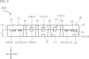
- FIG. 4 is a front view of the semiconductor device shown in FIG. 1.
- FIG. 5 is a right side view of the semiconductor device shown in FIG. 1.
- FIG. 6 is a cross-sectional view taken along line VI-VI of FIG.
- FIG. 7 is a cross-sectional view along line VII-VII of FIG.
- FIG. 8 is a cross-sectional view along line VIII-VIII of FIG.
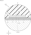
- FIG. 9 is a partial enlarged view of FIG. 6 showing the first element and its vicinity.
- FIG. 10 is a partially enlarged view of FIG.
- FIG. 11 is a cross-sectional view of a semiconductor device according to a modification of the first embodiment of the present disclosure
- FIG. 12 is a front view of a semiconductor device package according to the first embodiment of the present disclosure
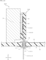
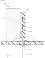
- FIG. 13 is a cross-sectional view taken along line XIII-XIII of FIG. 12.
- FIG. 14 is a cross-sectional view along line XIV-XIV in FIG. 12.
- FIG. 15 is a cross-sectional view of a semiconductor device according to a second embodiment of the present disclosure and a package of the semiconductor device.
- 16 is a plan view of a semiconductor device according to a third embodiment of the present disclosure
- FIG. 17 is a front view of the semiconductor device shown in FIG. 16.
- FIG. 16 is a plan view of a semiconductor device according to a third embodiment of the present disclosure
- FIG. 17 is a front view of the semiconductor device shown in FIG. 16.
- FIG. 16 is a plan view of a semiconductor device according to a third embodiment of the present disclosure
- FIG. 18 is a right side view of the semiconductor device shown in FIG. 16.
- FIG. 19 is a cross-sectional view along line XIX-XIX in FIG. 16.
- FIG. 20 is a cross-sectional view of a semiconductor device package according to a third embodiment of the present disclosure.
- FIG. 21 is a cross-sectional view of a semiconductor device according to a fourth embodiment of the present disclosure and a package of the semiconductor device. 22 is a right side view of the semiconductor device shown in FIG. 21.
- FIG. FIG. 23 is a cross-sectional view of a semiconductor device according to a fifth embodiment of the present disclosure and a package of the semiconductor device.
- FIG. 1 A semiconductor device A10 according to the first embodiment of the present disclosure will be described based on FIGS. 1 to 10.
- FIG. The semiconductor device A10 includes two die pads 10, three first terminals 11, two second terminals 12, two third terminals 13, a plurality of semiconductor elements 21, a first conducting member 31, a second conducting member 32, and A sealing resin 50 is provided. Further, semiconductor device A10 includes two first wires 41, two second wires 42, two first relay wires 43, and two second relay wires 44.
- FIG. 2 is transparent through the sealing resin 50 for convenience of understanding.
- the permeated sealing resin 50 is indicated by an imaginary line (chain double-dashed line).
- the VI-VI line, the VII-VII line and the VIII-VIII line are indicated by one-dot chain lines.
- first direction x A direction in which the two second terminals 12 extend is called "first direction x”.
- second direction y A direction perpendicular to the first direction x is called a “second direction y”.
- the second direction y corresponds to the normal direction of main surfaces 101 of two die pads 10, which will be described later.
- a direction orthogonal to the first direction x and the second direction y is called a “third direction z”.
- the semiconductor device A10 converts a DC power supply voltage applied to a first input terminal 11A and a second input terminal 11C out of three first terminals 11, which will be described later, into AC power using a plurality of semiconductor elements 21.
- the converted AC power is input from the output terminal 11B of the three first terminals 11 to a power supply object such as a motor.
- the semiconductor device A10 is used, for example, in a power conversion circuit such as an inverter.
- the two die pads 10 include a first pad 10A and a second pad 10B, as shown in FIGS.
- the first pad 10A and the second pad 10B are positioned apart from each other in the third direction z.
- Two die pads 10 are obtained from the same leadframe along with three first terminals 11, two second terminals 12 and two third terminals 13.
- the lead frame is copper (Cu) or a copper alloy. Therefore, the compositions of the two die pads 10, the three first terminals 11, the two second terminals 12, and the two third terminals 13 contain copper.
- Each of the two die pads 10 has a main surface 101 and a back surface 102 .
- the main surface 101 and the back surface 102 face opposite sides in the second direction y.
- the rear surface 102 is exposed outside from the sealing resin 50 .
- a first seat portion 103 is provided on the second pad 10B.
- the first seat portion 103 is recessed from the main surface 101 of the second pad 10B. Accordingly, in the second pad 10B, a step is formed between the main surface 101 and the first seat portion 103 .
- the sealing resin 50 covers the plurality of semiconductor elements 21, the first conductive members 31 and the second conductive members 32, as shown in FIGS. Furthermore, the sealing resin 50 partially covers each of the two die pads 10 , the three first terminals 11 , the two second terminals 12 , and the two third terminals 13 .
- the sealing resin 50 has electrical insulation.
- Sealing resin 50 is made of a material containing, for example, black epoxy resin.
- the sealing resin 50 has a top surface 51 , a bottom surface 52 , two first side surfaces 53 , a second side surface 54 , a third side surface 55 , a plurality of recesses 56 and grooves 57 .
- the top surface 51 faces the same side as the major surfaces 101 of the two die pads 10 in the second direction y.
- the bottom surface 52 faces away from the top surface 51 in the second direction y.
- the rear surface 102 of the first pad 10A and the rear surface 102 of the second pad 10B are exposed from the bottom surface 52 to the outside.
- the two first side surfaces 53 are located apart from each other in the third direction z.
- the two first side surfaces 53 face the third direction z and extend in the first direction x.
- Two first side surfaces 53 are connected to the top surface 51 and the bottom surface 52 .
- the second side 54 and the third side 55 are positioned apart from each other in the first direction x.
- the second side surface 54 and the third side surface 55 face opposite sides in the first direction x and extend in the third direction z.
- a second side surface 54 and a third side surface 55 are connected to the top surface 51 and the bottom surface 52 .
- three first terminals 11, two second terminals 12, and two third terminals 13 are exposed from the third side surface 55 to the outside.
- the plurality of recesses 56 are recessed from the third side surface 55 in the first direction x and reach the bottom surface 52 from the top surface 51 in the second direction y.
- the plurality of concave portions 56 are arranged between a first input terminal 11A and a first detection terminal 13A, which will be described later, between a first input terminal 11A and a second input terminal 11C, which will be described later, and an output terminal, which will be described later. 11B and the second input terminal 11C, and between the output terminal 11B and the second detection terminal 13B.
- the groove 57 is recessed from the bottom surface 52 in the second direction y and extends in the first direction x. Both sides of the groove portion 57 in the first direction x are connected to the second side surface 54 and the third side surface 55 . As viewed in the second direction y, the groove portion 57 divides the rear surface 102 of the first pad 10A and the rear surface 102 of the second pad 10B.
- a plurality of semiconductor elements 21 are mounted on each of the first pads 10A and the second pads 10B, as shown in FIGS.
- the multiple semiconductor elements 21 include two first elements 21A and two second elements 21B.
- the two first elements 21A are mounted on the main surface 101 of the first pad 10A.
- the two second elements 21B are mounted on the main surface 101 of the second pad 10B.
- the plurality of semiconductor elements 21 are, for example, MOSFETs (Metal-Oxide-Semiconductor Field-Effect Transistors).
- the plurality of semiconductor elements 21 may be switching elements such as IGBTs (Insulated Gate Bipolar Transistors) or diodes.
- the plurality of semiconductor elements 21 are n-channel MOSFETs with a vertical structure.
- the plurality of semiconductor elements 21 includes compound semiconductor substrates.
- the composition of the compound semiconductor substrate includes silicon carbide (SiC).
- SiC silicon carbide
- each of the plurality of semiconductor elements 21 has a first electrode 211, a second electrode 212, a gate electrode 213 and two detection electrodes 214.
- the first electrode 211 is located on the opposite side of the main surface 101 of either of the two die pads 10 in the second direction y. A current corresponding to the power converted by the semiconductor element 21 flows through the first electrode 211 . That is, the first electrode 211 corresponds to the source electrode of the semiconductor element 21 .
- the second electrode 212 faces one of the main surfaces 101 of the two die pads 10. As shown in FIGS. 9 and 10, the second electrode 212 faces one of the main surfaces 101 of the two die pads 10. As shown in FIGS. A current corresponding to the power before being converted by the semiconductor element 21 flows through the second electrode 212 . That is, the second electrode 212 corresponds to the drain electrode of the semiconductor element 21 .
- the gate electrode 213 is positioned on the same side as the first electrode 211 in the second direction y.
- a gate voltage for driving the semiconductor element 21 is applied to the gate electrode 213 .
- the area of the gate electrode 213 is smaller than the area of the first electrode 211 when viewed in the second direction y.
- the two detection electrodes 214 are positioned on the same side as the first electrode 211 in the second direction y.
- the two detection electrodes 214 are positioned opposite to each other with respect to the gate electrode 213 in the first direction x.
- a voltage having the same potential as that of the first electrode 211 is applied to each of the two detection electrodes 214 .
- the die bonding layer 23 is formed between the main surface 101 of the first pad 10A and the two first elements 21A and between the main surface 101 of the second pad 10B and the two second elements. 21B, respectively.
- the die bonding layer 23 has conductivity. Die bonding layer 23 is, for example, solder. Alternatively, the die bonding layer 23 may be a sintered metal.
- the die bonding layer 23 electrically connects the main surface 101 of the first pad 10A and the second electrodes 212 of the two first elements 21A. Thereby, the second electrodes 212 of the two first elements 21A are electrically connected to the first pad 10A.
- the die bonding layer 23 electrically connects the main surface 101 of the second pad 10B and the second electrodes 212 of the two second elements 21B. Thereby, the second electrodes 212 of the two second elements 21B are electrically connected to the second pads 10B.
- the three first terminals 11 are located on the opposite side of the second side surface 54 of the sealing resin 50 with the two die pads 10 as the reference in the first direction x, as shown in FIG.
- the three first terminals 11 are electrically connected to the plurality of semiconductor elements 21 .
- the three first terminals 11 include a first input terminal 11A, an output terminal 11B and a second input terminal 11C.
- each of the three first terminals 11 has a first portion 111, a second portion 112 and a third portion 113.
- FIG. At least a portion of the first portion 111 extends in the first direction x.
- the first portion 111 extends from the third side surface 55 of the sealing resin 50 .
- the second portion 112 extends in the first direction x.
- the second part 112 is located apart from the first part 111 and the sealing resin 50 .
- the second part 112 overlaps the first part 111 when viewed in the second direction y.
- the third part 113 connects the first part 111 and the second part 112 .
- the third portion 113 is located on the opposite side of the sealing resin 50 with respect to the first portion 111 in the first direction x.
- the sealing resin 50 entirely overlaps each of the first portion 111 and the second portion 112 when viewed in the first direction x. .
- each of the three first terminals 11 has a covering portion 115. As shown in FIG. The covering portion 115 is located on the side opposite to the third portion 113 with respect to the first portion 111 in the first direction x. The covering portion 115 is connected to the first portion 111 . The covering portion 115 is covered with the sealing resin 50 .
- the covering portion 115 of the first input terminal 11A is connected to the first pad 10A, as shown in FIGS. Therefore, the first input terminal 11A is electrically connected to the second electrodes 212 of the two first elements 21A via the first pads 10A.
- the first input terminal 11A is a P terminal (positive electrode) to which a DC power supply voltage to be converted is applied.
- the covering portion 115 of the output terminal 11B is connected to the second pad 10B as shown in FIG. Therefore, the output terminal 11B is electrically connected to the second electrodes 212 of the two second elements 21B via the second pads 10B. AC power converted by the plurality of semiconductor elements 21 is output from the output terminal 11B.
- the second input terminal 11C is located away from the two die pads 10 in the first direction x, as shown in FIG.
- the second input terminal 11C is positioned between the first input terminal 11A and the output terminal 11B in the third direction z.
- the second input terminal 11C is electrically connected to the first electrodes 211 of the two second elements 21B.
- the second input terminal 11C is an N terminal (negative electrode) to which a DC power supply voltage to be converted is applied.
- a second seat portion 116 is provided on the covering portion 115 of the second input terminal 11C.
- the second seat portion 116 is recessed in the second direction y from the side on which the second base portion 321 of the second conducting member 32 described later is located.
- the two second terminals 12 are located on the opposite side of the second side surface 54 of the sealing resin 50 with the two die pads 10 as the reference in the first direction x, as shown in FIG. As shown in FIG. 2, the two second terminals 12 extend in the first direction x. Each of the two second terminals 12 is positioned away from the three first terminals 11 in the third direction z. The two second terminals 12 sandwich the three first terminals 11 and the two third terminals 13 in the third direction z.
- the two second terminals 12 include a first gate terminal 12A and a second gate terminal 12B.
- each of the two second terminals 12 has a first mounting portion 121, a second mounting portion 122 and a covering portion 123.
- FIG. The first mounting portion 121 extends from the third side surface 55 of the sealing resin 50 .
- the second mounting portion 122 is located on the opposite side of the sealing resin 50 with respect to the first mounting portion 121 in the first direction x.
- the second mounting portion 122 is connected to the first mounting portion 121 .
- the dimension of the second mounting portion 122 in the third direction z is smaller than the dimension of the first mounting portion 121 in the third direction z.
- the covering portion 123 is located on the side opposite to the second mounting portion 122 with respect to the first mounting portion 121 in the first direction x.
- the covering portion 123 is connected to the first mounting portion 121 .
- the covering portion 123 is covered with the sealing resin 50 .
- the first mounting portion 121 of each of the two second terminals 12 has a first edge 121A.
- the first edge 121A extends in the third direction z.
- the second mounting portion 122 of one of the two second terminals 12 is connected to the first edge 121A.
- the second mounting portions 122 of each of the three first terminals 11 are located on both sides of the first edge 121A in the first direction x.
- the first gate terminal 12A is positioned closer to the first pad 10A than the second pad 10B, as shown in FIG.
- the first gate terminal 12A is electrically connected to the gate electrodes 213 of the two first elements 21A.
- a gate voltage for driving the two first elements 21A is applied to the first gate terminal 12A.
- the second gate terminal 12B is located closer to the second pad 10B than the first pad 10A, as shown in FIG.
- the second gate terminal 12B is electrically connected to the gate electrodes 213 of the two second elements 21B.
- a gate voltage for driving the two second elements 21B is applied to the second gate terminal 12B.
- the two third terminals 13 are located on the opposite side of the second side surface 54 of the sealing resin 50 with the two die pads 10 as the reference in the first direction x, as shown in FIG. As shown in FIG. 2, the two third terminals 13 extend in the first direction x. Each of the two third terminals 13 is located away from the three first terminals 11 in the third direction z. The two third terminals 13 sandwich the three first terminals 11 in the third direction z.
- the two third terminals 13 include a first detection terminal 13A and a second detection terminal 13B.
- each of the two third terminals 13 has a mounting portion 131 and a covering portion 132 .
- the mounting portion 131 extends from the third side surface 55 of the sealing resin 50 .
- the covering portion 132 is connected to the mounting portion 131 and covered with the sealing resin 50 .
- the first detection terminal 13A is positioned between the first input terminal 11A and the first gate terminal 12A, as shown in FIG.
- the first detection terminal 13A is electrically connected to the two detection electrodes 214 of the two first elements 21A.
- a voltage having the same potential as the voltage applied to the first electrodes 211 of the two first elements 21A is applied to the first detection terminal 13A.
- the second detection terminal 13B is located between the output terminal 11B and the second gate terminal 12B, as shown in FIG.
- the second detection terminal 13B is electrically connected to two detection electrodes 214 of the two second elements 21B.
- a voltage having the same potential as the voltage applied to the first electrodes 211 of the two second elements 21B is applied to the second detection terminal 13B.
- the heights h of the first portions 111 of the three first terminals 11 are all the same.
- the first mounting portion 121 of one of the two second terminals 12 overlaps the first portion 111 of one of the three first terminals 11 when viewed in the third direction z.
- the first conductive member 31 is conductively joined to the first electrodes 211 of the two first elements 21A and the first seat portion 103 of the second pad 10B. Thereby, the first electrodes 211 of the two first elements 21A are electrically connected to the second pads 10B and the second electrodes 212 of the two second elements 21B.
- the composition of the first conduction member 31 contains copper.
- the first conductive member 31 is a metal clip.
- the first conducting member 31 has a first base portion 311 , two first joint portions 312 and a second joint portion 313 .
- the first base 311 extends in the third direction z. As shown in FIG. 6, the first base portion 311 straddles between the first pad 10A and the second pad 10B.
- the two first joints 312 are individually conductively joined to the first electrodes 211 of the two first elements 21A.
- Each of the two first joints 312 is bifurcated apart from each other in the first direction x.
- the two first joints 312 are positioned apart from each other in the first direction x.
- the two first joints 312 are connected to the first base 311 .
- the second joint portion 313 is conductively joined to the first seat portion 103 of the second pad 10B.
- the second joint portion 313 extends in the first direction x. At least part of the second joint portion 313 is accommodated in the first seat portion 103 .
- the second joint portion 313 is connected to the first base portion 311 .
- the second joint 313 is located on the opposite side of the first base 311 from the two first joints 312 in the third direction z.
- the semiconductor device A10 further includes a first bonding layer 33, as shown in FIGS.
- the first bonding layer 33 electrically connects the first electrodes 211 of the two first elements 21A and the two first bonding portions 312 .
- the first bonding layer 33 is solder, for example.
- the first bonding layer 33 may be a sintered metal.
- the semiconductor device A10 further includes a second bonding layer 34, as shown in FIG.
- the second bonding layer 34 conductively bonds the first seat portion 103 of the second pad 10B and the second bonding portion 313 .
- the second bonding layer 34 is solder, for example.
- the second bonding layer 34 may be a sintered metal.
- the second conductive member 32 is conductively joined to the first electrodes 211 of the two second elements 21B and the second seat portion 116 of the second input terminal 11C. Thereby, the second input terminal 11C is electrically connected to the first electrodes 211 of the two second elements 21B.
- the composition of the second conducting member 32 contains copper.
- the second conductive member 32 is a metal clip.
- the second conducting member 32 has a second base 321 , two third joints 322 and a fourth joint 323 .
- the second base 321 is bent like a hook when viewed in the second direction y.
- the second base portion 321 overlaps the main surface 101 of the second pad 10B.
- the two third joints 322 are individually conductively joined to the first electrodes 211 of the two second elements 21B.
- Each of the two third joints 322 is bifurcated apart from each other in the first direction x.
- the two third joints 322 are positioned apart from each other in the first direction x.
- the two third joints 322 are connected to the second base 321 .
- the fourth joint portion 323 is conductively joined to the second seat portion 116 of the second input terminal 11C.
- the fourth joint portion 323 extends in the third direction z. At least part of the fourth joint portion 323 is accommodated in the second seat portion 116 .
- the fourth joint portion 323 is connected to the second base portion 321 .
- the semiconductor device A10 further includes a third bonding layer 35, as shown in FIGS.
- the third bonding layer 35 electrically connects the first electrodes 211 of the two second elements 21B and the two third bonding portions 322 .
- the third bonding layer 35 is solder, for example.
- the third bonding layer 35 may be a sintered metal.
- the semiconductor device A10 further includes a fourth bonding layer 36, as shown in FIG.
- the fourth bonding layer 36 conductively bonds the second seat portion 116 of the second input terminal 11 ⁇ /b>C and the fourth bonding portion 323 .
- the fourth bonding layer 36 is solder, for example.
- the fourth bonding layer 36 may be a sintered metal.
- One of the two first wires 41 is connected to the gate electrode 213 of the first element 21A located closest to the first gate terminal 12A of the two first elements 21A. and the covering portion 123 of the first gate terminal 12A.
- the other first wire 41 of the two first wires 41 is, as shown in FIG. and the covering portion 123 of the second gate terminal 12B.
- One first relay wire 43 of the two first relay wires 43 is electrically conductive to the gate electrode 213 of one first element 21A and the gate electrode 213 of the other first element 21A, as shown in FIG. are spliced.
- the other first relay wire 43 of the two first relay wires 43 is, as shown in FIG. are spliced.
- the two first wires 41 and the two first relay wires 43 electrically connect the first gate terminal 12A to the gate electrodes 213 of the two first elements 21A.
- the second gate terminal 12B is electrically connected to the gate electrode 213 of each of the two second elements 21B.
- One of the two second wires 42 is, as shown in FIG. Any one of the electrodes 214 is conductively joined to the covering portion 132 of the first detection terminal 13A.
- the other second wire 42 of the two second wires 42 is, as shown in FIG. Either of the electrodes 214 is conductively joined to the covering portion 132 of the second detection terminal 13B.
- One of the two second relay wires 44 is, as shown in FIG. It is conductively joined to one of the sensing electrodes 214 .
- the other second relay wire 44 of the two second relay wires 44 is, as shown in FIG. It is conductively joined to one of the sensing electrodes 214 .
- the two second wires 42 and the two second relay wires 44 electrically connect the first detection terminal 13A to the two detection electrodes 214 of each of the two first elements 21A.
- the second detection terminal 13B is electrically connected to each of the two detection electrodes 214 of the two second elements 21B.
- each of the three first terminals 11 does not have the third portion 113 in the semiconductor device A11.
- the second portion 112 is joined to the first portion 111 by welding or the like. Therefore, the second portion 112 is in contact with the first portion 111 .
- the mounting body B10 includes a semiconductor device A10, a wiring board 60, a bonding layer 69, and a heat dissipation member .
- FIG. 14 omits illustration of the bonding layer 69 for convenience of understanding.
- the XIII-XIII line is indicated by a dashed line.
- the wiring board 60 is a mounting target of the semiconductor device A10.
- Wiring board 60 is, for example, a PCB.
- the wiring board 60 has a base material 61 and wiring 62 .
- the base material 61 is provided with a plurality of through holes 611 .
- a plurality of through holes 611 pass through the base material 61 in the first direction x.
- each of the plurality of through holes 611 is an elongated hole extending in the second direction y.
- the wiring 62 is adjacent to a plurality of through holes 611, as shown in FIGS.
- the wiring 62 is electrically connected to a DC power supply arranged outside the mounting body B10, a gate driver and a controller (both not shown) mounted on the wiring board 60, and the like.
- the three first terminals 11, the two second terminals 12, and the two third terminals 13 of the semiconductor device A10 are individually inserted through the plurality of through holes 611 of the substrate 61. .
- the three first terminals 11 , the two second terminals 12 and the three third terminals 13 are conductively joined to the wiring 62 by the joining layer 69 . Therefore, the semiconductor device A10 is through-hole mounted in the mounting body B10.
- the bonding layer 69 is solder, for example.
- each of the first portion 111 and the second portion 112 of each of the three first terminals 11 is housed in one of the plurality of through holes 611 of the base material 61 .
- the heat dissipation member 70 is attached to the sealing resin 50 of the semiconductor device A10.
- the heat dissipation member 70 faces the rear surfaces 102 of the two die pads 10 .
- Heat dissipation member 70 is, for example, a heat sink.
- the semiconductor device A10 has a first terminal 11 electrically connected to the semiconductor element 21 .
- the first terminal 11 has a first portion 111 at least partially extending in the first direction x and a second portion 112 extending in the first direction x.
- the second part 112 overlaps the first part 111 when viewed in the second direction y.
- a part of each of first portion 111 and second portion 112 is accommodated in through hole 611 provided in base material 61 of wiring board 60. As shown in FIG. With this configuration, the contact area of the first terminal 11 with the bonding layer 69 is increased, so that the heat conducted from the semiconductor element 21 to the first terminal 11 is easily radiated from the bonding layer 69 to the outside.
- the temperature rise of the wiring substrate 60 can be suppressed, and the current that can be conducted to the first terminal 11 can be increased. Furthermore, it contributes to the improvement of heat dissipation of the semiconductor device A10. Therefore, according to the semiconductor device A10 and the mounting body B10, it is possible to improve the reliability of the semiconductor device A10 that is through-hole mounted.
- the first terminal 11 has a third portion 113 connecting the first portion 111 and the second portion 112 . Furthermore, the second part 112 is located away from the first part 111 . By adopting this configuration, the contact area of the first terminal 11 with the bonding layer 69 is further increased in the mounting body B10.
- the semiconductor device A10 further includes a sealing resin 50 that covers part of the first terminals 11 and the semiconductor element 21 .
- the second portion 112 of the first terminal 11 is located away from the sealing resin 50 .
- the sealing resin 50 overlaps the first portion 111 and the second portion 112 .
- the semiconductor device A10 further includes a second terminal 12 extending in the first direction x and partially covered with the sealing resin 50 .
- the second terminal 12 is positioned apart from the first terminal 11 in the third direction z.
- the second terminal 12 has a first mounting portion 121 and a second mounting portion 122 .
- the second mounting portion 122 is located on the opposite side of the sealing resin 50 with respect to the first mounting portion 121 in the first direction x.
- the dimension of the second mounting portion 122 in the third direction z is smaller than the dimension of the first mounting portion 121 in the third direction z.
- the first mounting portion 121 of the second terminal 12 extends in the third direction z and has a first edge 121A to which the second mounting portion 122 is connected.
- the second portion 112 of the first terminal 11 is located on both sides of the first edge 121A in the first direction x.
- a through hole 611 of the base material 61 is an elongated hole extending in the second direction y.
- the sealing resin 50 has a plurality of recesses 56 recessed from the third side surface 55 in the first direction x. This configuration ensures a longer creepage distance of the sealing resin 50 between any two of the three first terminals 11 . Thereby, the withstand voltage of the semiconductor device A10 can be improved.
- the sealing resin 50 has a groove portion 57 which is recessed from the bottom surface 52 and separates the back surface 102 of the first pad 10A and the back surface 102 of the second pad 10B when viewed in the second direction y.
- a longer creepage distance of the sealing resin 50 between the two die pads 10 is ensured. This makes it possible to further improve the withstand voltage of the semiconductor device A10.
- the thermal strain of the sealing resin 50 in the third direction z is dispersed. As a result, concentration of thermal strain on the two first side surfaces 53 of the sealing resin 50 can be alleviated.
- each of the first input terminal 11A and the output terminal 11B is connected to one of the two die pads 10.
- the two die pads 10 can be utilized as conductive members while suppressing an increase in the size of the semiconductor device A10.
- the rear surfaces 102 of the two die pads 10 are exposed from the sealing resin 50 . Thereby, the heat dissipation of the semiconductor device A10 can be improved.
- the composition of the first conduction member 31 and the second conduction member 32 contains copper.
- the electric resistance of the first conducting member 31 and the second conducting member 32 can be reduced as compared with a wire containing aluminum in its composition. This is suitable for allowing a larger current to flow through the semiconductor element 21 .
- FIG. 15 Based on FIG. 15, a semiconductor device A20 according to the second embodiment of the present disclosure and a semiconductor device package (hereinafter referred to as a “package B20”) according to the second embodiment of the present disclosure will be described.
- a semiconductor device package hereinafter referred to as a “package B20”
- elements that are the same as or similar to those of the semiconductor device A10 and the mounting body B10 described above are denoted by the same reference numerals, and overlapping descriptions are omitted.
- the cross-sectional position of FIG. 15 is the same as the cross-sectional position of FIG. 13 showing the mounting body B10.
- the mounting body B20 includes a semiconductor device A20, a wiring board 60, a bonding layer 69, and a heat dissipation member 70.
- the configuration of the three first terminals 11 is different from that of the semiconductor device A10 and the mounting body B10.
- the third portion 113 protrudes from the first portion 111 and the second portion 112 when viewed in the first direction x.
- the third portion 113 protrudes in the second direction y.
- the semiconductor device A20 has a first terminal 11 electrically connected to the semiconductor element 21 .
- the first terminal 11 has a first portion 111 at least partially extending in the first direction x and a second portion 112 extending in the first direction x.
- the second part 112 overlaps the first part 111 when viewed in the second direction y.
- a part of each of first portion 111 and second portion 112 is accommodated in through hole 611 provided in base material 61 of wiring board 60. As shown in FIG. Therefore, the semiconductor device A20 and the mounting body B20 can also improve the reliability of the through-hole mounted semiconductor device A20.
- the third portion 113 of the first terminal 11 protrudes from the first portion 111 and the second portion 112 of the first terminal 11 when viewed in the first direction x.
- a semiconductor device A30 according to the third embodiment of the present disclosure and a semiconductor device package (hereinafter referred to as a “package B30”) according to the third embodiment of the present disclosure will be described with reference to FIGS. .
- FIGS. In these figures, elements that are the same as or similar to those of the semiconductor device A10 and the mounting body B10 described above are denoted by the same reference numerals, and overlapping descriptions are omitted.
- the XIX-XIX line is indicated by a one-dot chain line.
- a mounted body B30 includes a semiconductor device A30, a wiring board 60, a bonding layer 69, and a heat dissipation member .
- the configuration of the three first terminals 11 is different from that of the semiconductor device A10 and the mounting body B10.
- each of the three first terminals 11 of the semiconductor device A30 has a fourth portion 114.
- FIG. The fourth portion 114 is located on the opposite side of the third portion 113 with respect to the second portion 112 in the first direction x.
- the fourth section 114 is connected to the second section 112 .
- the fourth portion 114 extends to the side opposite to the side where the first portion 111 is located in the second direction y.
- the fourth portions 114 of the three first terminals 11 are opposite to the third portions 113 of the three first terminals 11 with respect to the wiring board 60 in the first direction x. located on the side.
- the semiconductor device A30 has a first terminal 11 electrically connected to the semiconductor element 21 .
- the first terminal 11 has a first portion 111 at least partially extending in the first direction x and a second portion 112 extending in the first direction x.
- the second part 112 overlaps the first part 111 when viewed in the second direction y.
- mounting body B ⁇ b>30 a portion of each of first portion 111 and second portion 112 is accommodated in through hole 611 provided in base material 61 of wiring board 60 . Therefore, the semiconductor device A30 and the mounting body B30 can also improve the reliability of the through-hole mounted semiconductor device A30.
- the first terminal 11 has a fourth portion 114 connected to the second portion 112.
- the fourth portion 114 is located on the side opposite to the side on which the first portion 111 of the first terminal 11 is located in the second direction y.
- FIG. 21 a semiconductor device A40 according to the fourth embodiment of the present disclosure and a semiconductor device package (hereinafter referred to as a "package B40") according to the fourth embodiment of the present disclosure will be described.
- a semiconductor device package hereinafter referred to as a "package B40"
- FIG. 21 elements that are the same as or similar to those of the semiconductor device A10 and the mounting body B10 described above are denoted by the same reference numerals, and overlapping descriptions are omitted.
- the cross-sectional position of FIG. 21 is the same as the cross-sectional position of FIG. 13 showing the mounting body B10.
- a mounted body B40 includes a semiconductor device A40, a wiring board 60, a bonding layer 69, and a heat dissipation member 70.
- the arrangement configuration of the semiconductor device A40 is different from the configuration of the mounting body B10.
- the semiconductor device A40 has three first terminals 11, two second terminals 12, and two third terminals 13 of the semiconductor device A10 arranged at 90 degrees around the third direction z. It is bent to Accordingly, in the semiconductor device A40, the normal direction of the main surfaces 101 of the two die pads 10 is the first direction x. Furthermore, in the mounting body B40, the first portion 111 of each of the three first terminals 11 is located between the sealing resin 50 and the second portion 112 of the first terminal 11 in the second direction y.
- the semiconductor device A40 has a first terminal 11 electrically connected to the semiconductor element 21 .
- the first terminal 11 has a first portion 111 at least partially extending in the first direction x and a second portion 112 extending in the first direction x.
- the second part 112 overlaps the first part 111 when viewed in the second direction y.
- a part of each of first portion 111 and second portion 112 is accommodated in through hole 611 provided in base material 61 of wiring board 60. As shown in FIG. Therefore, the semiconductor device A40 and the mounting body B40 can also improve the reliability of the through-hole mounted semiconductor device A40.
- FIG. 23 Based on FIG. 23, a semiconductor device A50 according to the fifth embodiment of the present disclosure and a semiconductor device package (hereinafter referred to as a “package B50”) according to the fifth embodiment of the present disclosure will be described.
- the same or similar elements as those of the semiconductor device A10 and the mounting body B10 described above are denoted by the same reference numerals, and overlapping descriptions are omitted.
- the cross-sectional position of FIG. 23 is the same as the cross-sectional position of FIG. 13 showing the mounting body B10.
- a mounted body B50 includes a semiconductor device A50, a wiring board 60, a bonding layer 69, and a heat dissipation member .
- the arrangement configuration of the semiconductor device A50 is different from the configuration of the mounting body B30 described above.
- the semiconductor device A50 has three first terminals 11, two second terminals 12, and two third terminals 13 of the semiconductor device A30 bent at 90° around the third direction z. It is what I did. Accordingly, in the semiconductor device A50, the normal direction of the main surfaces 101 of the two die pads 10 is the first direction x. Furthermore, in the mounting body B50, the first portion 111 of each of the three first terminals 11 is positioned between the sealing resin 50 and the second portion 112 of the first terminal 11 in the second direction y.
- the semiconductor device A50 has a first terminal 11 electrically connected to the semiconductor element 21 .
- the first terminal 11 has a first portion 111 at least partially extending in the first direction x and a second portion 112 extending in the first direction x.
- the second part 112 overlaps the first part 111 when viewed in the second direction y.
- a part of each of first portion 111 and second portion 112 is accommodated in through hole 611 provided in base material 61 of wiring board 60. As shown in FIG. Therefore, the semiconductor device A50 and the mounting body B50 can also improve the reliability of the through-hole mounted semiconductor device A50.
- Appendix 1 a semiconductor element; a first terminal electrically connected to the semiconductor element; The first terminal has a first portion at least partially extending in a first direction and a second portion extending in the first direction, The semiconductor device, wherein the second portion overlaps the first portion when viewed in a second direction orthogonal to the first direction.
- Appendix 2. The semiconductor device according to appendix 1, wherein the first terminal has a third portion connecting the first portion and the second portion.
- Appendix 3 The semiconductor device according to appendix 2, wherein the third portion protrudes from the first portion and the second portion when viewed in the first direction.
- Appendix 5. the first terminal has a fourth portion positioned opposite to the third portion with respect to the second portion in the first direction and connected to the second portion; 5.
- Appendix 6. further comprising a sealing resin covering a portion of the first terminal and the semiconductor element; The first part extends from the sealing resin, 6.
- Appendix 6 wherein the sealing resin overlaps the first portion and the second portion when viewed in the first direction.
- Appendix 8. further comprising a second terminal extending in the first direction and partially covered with the sealing resin; the second terminal is positioned away from the first terminal in a third direction orthogonal to the first direction and the second direction; The second terminal is located on a side opposite to the sealing resin with respect to the first mounting portion extending from the sealing resin and the first mounting portion in the first direction, and is attached to the first mounting portion. and a second mounting portion connected, 8.
- the semiconductor device according to appendix 8 wherein the first mounting portion overlaps the first portion when viewed in the third direction.
- Appendix 10. the first mounting portion has a first edge extending in the third direction and connected to the second mounting portion; 10.
- Appendix 11. further equipped with a die pad, 11.
- Appendix 12. 12.
- Appendix 13. The die pad has a back surface facing the side opposite to the side facing the semiconductor element in the second direction, 13.
- Appendix 14 a semiconductor device according to any one of Appendices 6 to 13; a wiring board having a base material and wiring arranged on the base material; a bonding layer that conductively bonds the wiring and the first terminal; the base material is provided with a through hole adjacent to the wiring and penetrating the base material in the first direction; A mounted body of a semiconductor device, wherein a part of each of the first part and the second part is housed in the through hole.
- Appendix 15. 15.
- Appendix 14 or 15 wherein the first portion is positioned between the sealing resin and the second portion in the second direction.
- Appendix 17. further comprising a heat dissipating member, 17.
Landscapes
- Engineering & Computer Science (AREA)
- Microelectronics & Electronic Packaging (AREA)
- Manufacturing & Machinery (AREA)
- Structures Or Materials For Encapsulating Or Coating Semiconductor Devices Or Solid State Devices (AREA)
Priority Applications (4)
| Application Number | Priority Date | Filing Date | Title |
|---|---|---|---|
| DE112022004162.5T DE112022004162T5 (de) | 2021-12-14 | 2022-12-02 | Halbleiterbauteil, und halbleiterbauteil-montagekörper |
| JP2023567693A JPWO2023112723A1 (https=) | 2021-12-14 | 2022-12-02 | |
| CN202280081786.7A CN118435348A (zh) | 2021-12-14 | 2022-12-02 | 半导体装置以及半导体装置的安装体 |
| US18/652,417 US20240282681A1 (en) | 2021-12-14 | 2024-05-01 | Semiconductor device, and semiconductor device mounting body |
Applications Claiming Priority (2)
| Application Number | Priority Date | Filing Date | Title |
|---|---|---|---|
| JP2021-202614 | 2021-12-14 | ||
| JP2021202614 | 2021-12-14 |
Related Child Applications (1)
| Application Number | Title | Priority Date | Filing Date |
|---|---|---|---|
| US18/652,417 Continuation US20240282681A1 (en) | 2021-12-14 | 2024-05-01 | Semiconductor device, and semiconductor device mounting body |
Publications (1)
| Publication Number | Publication Date |
|---|---|
| WO2023112723A1 true WO2023112723A1 (ja) | 2023-06-22 |
Family
ID=86774296
Family Applications (1)
| Application Number | Title | Priority Date | Filing Date |
|---|---|---|---|
| PCT/JP2022/044545 Ceased WO2023112723A1 (ja) | 2021-12-14 | 2022-12-02 | 半導体装置、および半導体装置の実装体 |
Country Status (5)
| Country | Link |
|---|---|
| US (1) | US20240282681A1 (https=) |
| JP (1) | JPWO2023112723A1 (https=) |
| CN (1) | CN118435348A (https=) |
| DE (1) | DE112022004162T5 (https=) |
| WO (1) | WO2023112723A1 (https=) |
Citations (5)
| Publication number | Priority date | Publication date | Assignee | Title |
|---|---|---|---|---|
| JPS327516Y1 (https=) * | 1955-05-23 | 1957-07-19 | ||
| JPS58116221U (ja) * | 1982-01-30 | 1983-08-08 | ニチコン株式会社 | 有極性電子部品 |
| JP2000208896A (ja) * | 1999-01-13 | 2000-07-28 | Fuji Electric Co Ltd | 電子部品搭載モジュ―ル及び電子部品搭載方法 |
| US20160365296A1 (en) * | 2015-06-09 | 2016-12-15 | Infineon Technologies Ag | Electronic Devices with Increased Creepage Distances |
| WO2021131611A1 (ja) * | 2019-12-25 | 2021-07-01 | ローム株式会社 | 半導体モジュール |
-
2022
- 2022-12-02 DE DE112022004162.5T patent/DE112022004162T5/de active Pending
- 2022-12-02 JP JP2023567693A patent/JPWO2023112723A1/ja active Pending
- 2022-12-02 CN CN202280081786.7A patent/CN118435348A/zh active Pending
- 2022-12-02 WO PCT/JP2022/044545 patent/WO2023112723A1/ja not_active Ceased
-
2024
- 2024-05-01 US US18/652,417 patent/US20240282681A1/en active Pending
Patent Citations (5)
| Publication number | Priority date | Publication date | Assignee | Title |
|---|---|---|---|---|
| JPS327516Y1 (https=) * | 1955-05-23 | 1957-07-19 | ||
| JPS58116221U (ja) * | 1982-01-30 | 1983-08-08 | ニチコン株式会社 | 有極性電子部品 |
| JP2000208896A (ja) * | 1999-01-13 | 2000-07-28 | Fuji Electric Co Ltd | 電子部品搭載モジュ―ル及び電子部品搭載方法 |
| US20160365296A1 (en) * | 2015-06-09 | 2016-12-15 | Infineon Technologies Ag | Electronic Devices with Increased Creepage Distances |
| WO2021131611A1 (ja) * | 2019-12-25 | 2021-07-01 | ローム株式会社 | 半導体モジュール |
Also Published As
| Publication number | Publication date |
|---|---|
| DE112022004162T5 (de) | 2024-06-13 |
| US20240282681A1 (en) | 2024-08-22 |
| JPWO2023112723A1 (https=) | 2023-06-22 |
| CN118435348A (zh) | 2024-08-02 |
Similar Documents
| Publication | Publication Date | Title |
|---|---|---|
| JP7267930B2 (ja) | 半導体装置 | |
| CN103314437B (zh) | 功率半导体模块及电源单元装置 | |
| WO2019235146A1 (ja) | 半導体モジュール | |
| WO2023162722A1 (ja) | 半導体装置および半導体モジュール | |
| WO2024116873A1 (ja) | 半導体モジュール | |
| WO2023112662A1 (ja) | 半導体モジュールおよび半導体装置 | |
| WO2025142335A1 (ja) | 半導体装置 | |
| WO2023112723A1 (ja) | 半導体装置、および半導体装置の実装体 | |
| WO2024018790A1 (ja) | 半導体装置 | |
| WO2020149225A1 (ja) | 半導体装置 | |
| WO2024176740A1 (ja) | 半導体装置および車両 | |
| WO2024029336A1 (ja) | 半導体装置 | |
| WO2023243278A1 (ja) | 半導体装置 | |
| WO2023149257A1 (ja) | 半導体装置 | |
| WO2023047890A1 (ja) | 半導体モジュール | |
| JP2023134143A (ja) | 半導体モジュール、半導体装置、及び車両 | |
| WO2022080081A1 (ja) | 半導体装置 | |
| JP7704594B2 (ja) | 半導体装置 | |
| WO2023218943A1 (ja) | 半導体装置 | |
| WO2024018851A1 (ja) | 半導体装置 | |
| WO2025177840A1 (ja) | 半導体装置および車両 | |
| WO2022168618A1 (ja) | 半導体装置 | |
| WO2023120185A1 (ja) | 半導体装置 | |
| WO2024128062A1 (ja) | 半導体装置 | |
| WO2022259809A1 (ja) | 半導体装置 |
Legal Events
| Date | Code | Title | Description |
|---|---|---|---|
| 121 | Ep: the epo has been informed by wipo that ep was designated in this application |
Ref document number: 22907251 Country of ref document: EP Kind code of ref document: A1 |
|
| ENP | Entry into the national phase |
Ref document number: 2023567693 Country of ref document: JP Kind code of ref document: A |
|
| WWE | Wipo information: entry into national phase |
Ref document number: 202280081786.7 Country of ref document: CN |
|
| 122 | Ep: pct application non-entry in european phase |
Ref document number: 22907251 Country of ref document: EP Kind code of ref document: A1 |