WO2023105845A1 - 共振子及び共振装置 - Google Patents
共振子及び共振装置 Download PDFInfo
- Publication number
- WO2023105845A1 WO2023105845A1 PCT/JP2022/029124 JP2022029124W WO2023105845A1 WO 2023105845 A1 WO2023105845 A1 WO 2023105845A1 JP 2022029124 W JP2022029124 W JP 2022029124W WO 2023105845 A1 WO2023105845 A1 WO 2023105845A1
- Authority
- WO
- WIPO (PCT)
- Prior art keywords
- vibrating
- thickness
- substrate
- resonator
- support
- Prior art date
- Legal status (The legal status is an assumption and is not a legal conclusion. Google has not performed a legal analysis and makes no representation as to the accuracy of the status listed.)
- Ceased
Links
Images


Classifications
-
- H—ELECTRICITY
- H03—ELECTRONIC CIRCUITRY
- H03H—IMPEDANCE NETWORKS, e.g. RESONANT CIRCUITS; RESONATORS
- H03H9/00—Networks comprising electromechanical or electro-acoustic elements; Electromechanical resonators
- H03H9/15—Constructional features of resonators consisting of piezoelectric or electrostrictive material
- H03H9/17—Constructional features of resonators consisting of piezoelectric or electrostrictive material having a single resonator
- H03H9/171—Constructional features of resonators consisting of piezoelectric or electrostrictive material having a single resonator implemented with thin-film techniques, i.e. of the film bulk acoustic resonator [FBAR] type
-
- H—ELECTRICITY
- H03—ELECTRONIC CIRCUITRY
- H03H—IMPEDANCE NETWORKS, e.g. RESONANT CIRCUITS; RESONATORS
- H03H9/00—Networks comprising electromechanical or electro-acoustic elements; Electromechanical resonators
- H03H9/02—Details
- H03H9/02007—Details of bulk acoustic wave devices
- H03H9/02086—Means for compensation or elimination of undesirable effects
- H03H9/02102—Means for compensation or elimination of undesirable effects of temperature influence
-
- H—ELECTRICITY
- H03—ELECTRONIC CIRCUITRY
- H03H—IMPEDANCE NETWORKS, e.g. RESONANT CIRCUITS; RESONATORS
- H03H9/00—Networks comprising electromechanical or electro-acoustic elements; Electromechanical resonators
- H03H9/02—Details
- H03H9/02244—Details of microelectro-mechanical resonators
- H03H9/02433—Means for compensation or elimination of undesired effects
- H03H9/02448—Means for compensation or elimination of undesired effects of temperature influence
-
- H—ELECTRICITY
- H03—ELECTRONIC CIRCUITRY
- H03H—IMPEDANCE NETWORKS, e.g. RESONANT CIRCUITS; RESONATORS
- H03H9/00—Networks comprising electromechanical or electro-acoustic elements; Electromechanical resonators
- H03H9/02—Details
- H03H9/05—Holders or supports
- H03H9/10—Mounting in enclosures
- H03H9/1057—Mounting in enclosures for microelectro-mechanical devices
-
- H—ELECTRICITY
- H03—ELECTRONIC CIRCUITRY
- H03H—IMPEDANCE NETWORKS, e.g. RESONANT CIRCUITS; RESONATORS
- H03H9/00—Networks comprising electromechanical or electro-acoustic elements; Electromechanical resonators
- H03H9/15—Constructional features of resonators consisting of piezoelectric or electrostrictive material
- H03H9/17—Constructional features of resonators consisting of piezoelectric or electrostrictive material having a single resonator
- H03H9/19—Constructional features of resonators consisting of piezoelectric or electrostrictive material having a single resonator consisting of quartz
-
- H—ELECTRICITY
- H03—ELECTRONIC CIRCUITRY
- H03H—IMPEDANCE NETWORKS, e.g. RESONANT CIRCUITS; RESONATORS
- H03H9/00—Networks comprising electromechanical or electro-acoustic elements; Electromechanical resonators
- H03H9/24—Constructional features of resonators of material which is not piezoelectric, electrostrictive, or magnetostrictive
-
- H—ELECTRICITY
- H03—ELECTRONIC CIRCUITRY
- H03H—IMPEDANCE NETWORKS, e.g. RESONANT CIRCUITS; RESONATORS
- H03H9/00—Networks comprising electromechanical or electro-acoustic elements; Electromechanical resonators
- H03H9/15—Constructional features of resonators consisting of piezoelectric or electrostrictive material
- H03H2009/155—Constructional features of resonators consisting of piezoelectric or electrostrictive material using MEMS techniques
Definitions
- the present invention relates to resonators and resonator devices.
- Patent Document 1 discloses a piezoelectric vibrator that includes a vibrating portion that performs contour vibration and a holding portion that has holding arms that hold the vibrating portion. ing.
- the vibrating portion has a structure in which a silicon oxide film, a silicon layer, a lower electrode, a piezoelectric film, a first adjustment film, and a second adjustment film are laminated.
- vibration may leak from the vibrating portion to the holding portion. Therefore, it is required to further improve the vibration confinement property (Q value) by suppressing such vibration leakage.
- the present invention has been made in view of such circumstances, and an object of the present invention is to provide a resonator and a resonance device capable of improving the confinement of vibration.
- a resonator includes a substrate and a piezoelectric layer provided on a main surface of the substrate and vibrating along the main surface of the substrate in response to an applied voltage.
- a holding portion provided around at least a portion of the vibrating portion in plan view on the main surface of the substrate; and a support portion provided between the holding portion and the vibrating portion to support the vibrating portion.
- the vibrating portion has a first portion that is a part of the main surface of the substrate when viewed in plan and a second portion that is another area of the main surface of the substrate when viewed in plan;
- the thickness of the second portion in the thickness direction intersecting the plane is greater than the thickness of the first portion in the thickness direction, and the vibrating portion is formed by the first portion and the second portion.
- the side opposite to the piezoelectric layer is configured to be concave or convex.
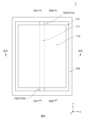
- FIG. 1 is an exploded perspective view schematically showing the configuration of a resonance device according to a first embodiment
- FIG. 1 is a cross-sectional view schematically showing the structure of a resonator according to a first embodiment
- FIG. FIG. 5 is a cross-sectional view schematically showing the structure of a resonator according to a second embodiment
- FIG. 11 is a cross-sectional view schematically showing the structure of a resonator according to a third embodiment
- FIG. 11 is a cross-sectional view schematically showing the structure of a resonator according to a fourth embodiment
- FIG. 11 is a cross-sectional view schematically showing the structure of a resonator according to a fifth embodiment
- FIG. 11 is a cross-sectional view schematically showing the structure of a resonator according to a sixth embodiment;
- FIG. 11 is a plan view schematically showing the structure of a resonator according to a seventh embodiment;
- FIG. 9 is a cross-sectional view of the resonator according to the seventh embodiment taken along line IXA-IXA in FIG. 8;
- FIG. 9 is a cross-sectional view of the resonator according to the seventh embodiment taken along line IXB-IXB in FIG. 8;
- FIG. 9 is a cross-sectional view of the resonator according to the seventh embodiment taken along line IXC-IXC in FIG. 8;
- FIG. 20 is a plan view schematically showing the structure of a resonator according to an eighth embodiment
- FIG. 11 is a cross-sectional view of the resonator according to the eighth embodiment taken along line XIA-XIA in FIG. 10
- FIG. 11 is a cross-sectional view of the resonator according to the eighth embodiment taken along line XIB-XIB in FIG. 10
- FIG. 11 is a cross-sectional view of the resonator according to the eighth embodiment taken along line XIC-XIC in FIG. 10
- FIG. 21 is a plan view schematically showing the structure of a resonator according to a ninth embodiment
- FIG. 13 is a cross-sectional view of the resonator according to the ninth embodiment taken along line XIIIA-XIIIA in FIG. 12;
- FIG. 13 is a cross-sectional view of the resonator according to the ninth embodiment taken along line XIIIB-XIIIB in FIG. 12;
- FIG. 13 is a cross-sectional view of the resonator according to the ninth embodiment taken along line XIIIC-XIIIC of FIG. 12;
- FIG. 20 is a plan view schematically showing the structure of a resonator according to a tenth embodiment;
- FIG. 15 is a cross-sectional view of the resonator according to the tenth embodiment taken along line XVA-XVIA in FIG. 14;
- FIG. 15 is a cross-sectional view of the resonator according to the tenth embodiment taken along line XVB-XVB in FIG. 14;
- FIG. 15 is a cross-sectional view of the resonator according to the tenth embodiment taken along line XVC-XVC in FIG. 14;
- FIG. 21 is a cross-sectional view schematically showing the structure of a resonator according to an eleventh embodiment;
- FIG. 1 is an exploded perspective view schematically showing the configuration of the resonator according to this embodiment.
- FIG. 2 is a cross-sectional view schematically showing the structure of the resonator according to the first embodiment.
- Each drawing is provided with an orthogonal coordinate system consisting of X, Y and Z axes for convenience in order to clarify the relationship between each drawing and to help understand the positional relationship of each member.
- Directions parallel to the X-axis, Y-axis and Z-axis are called the X-axis direction, the Y-axis direction and the Z-axis direction, respectively.
- the positive direction of the Z-axis (the direction of the arrow of the Z-axis) is defined as "up”
- the negative direction of the Z-axis (the direction opposite to the direction of the arrow of the Z-axis) is defined as "down”.
- a plane defined by the X-axis and the Y-axis is defined as the XY plane, and the same applies to the YZ plane and the ZX plane.
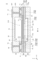
- the resonator 1 includes a resonator 15, a lower lid 20, and an upper lid 30 arranged to face the lower lid 20 with the resonator 15 interposed therebetween.
- a lower lid 20, a resonator 15, and an upper lid 30 are stacked in this order in the Z-axis direction.
- the resonator 15 and the lower lid 20 are joined together to form a MEMS substrate 50 .
- the upper lid 30 is bonded to the resonator 15 side of the MEMS substrate 50 .
- the upper lid 30 is joined to the lower lid 20 via the resonator 15 .
- the lower lid 20 and the upper lid 30 correspond to a package structure having a vibration space inside for vibrating the vibrating section 110 to be described later.
- the resonator 15 is a MEMS vibration element manufactured using MEMS technology.
- the frequency band of the resonator 15 is, for example, 1 kHz or more and 1 MHz or less.
- the resonator 15 is formed, for example, plane-symmetrical with respect to the YZ plane that bisects the resonator 15 in the X-axis direction.
- the resonator 15 includes a vibrating portion 110 , a holding portion 140 and a supporting portion 150 .
- the vibrating section 110 vibrates according to the applied alternating voltage.
- the vibration part 110 is held so as to vibrate in a vibration space provided between the lower lid 20 and the upper lid 30 .
- the vibrating portion 110 extends along the XY plane when not vibrating (when voltage is not applied), and stretches and vibrates in the X-axis direction when vibrating (when voltage is applied). That is, the vibrating section 110 vibrates in the widening vibration mode.
- the vibrating section 110 is provided in a plate shape having a main surface extending in the XY plane.
- the shape of the vibrating portion 110 is a pair of short electrodes extending in the X-axis direction and facing each other in the Y-axis direction. It has a rectangular shape having sides and a pair of long sides extending in the Y-axis direction and facing in the X-axis direction. Note that the shape of the vibrating portion 110 is not limited to the above, as long as the vibrating portion 110 can vibrate in the widening vibration mode.
- the holding part 140 forms a vibration space of the package structure together with the lower lid 20 and the upper lid 30 .
- the holding portion 140 is provided in a frame shape so as to surround the vibrating portion 110 when viewed from above.
- the holding portion 140 has a first frame portion 141A, a second frame portion 141B, a third frame portion 141C and a fourth frame portion 141D.
- the first frame portion 141A extends in the X-axis direction on the Y-axis positive direction side of the vibrating portion 110 .
- the second frame portion 141B extends in the X-axis direction on the Y-axis negative direction side of the vibrating portion 110 .
- the third frame portion 141C extends in the Y-axis direction on the X-axis negative direction side of the vibrating portion 110 .
- the fourth frame portion 141D extends in the Y-axis direction on the X-axis positive direction side of the vibrating portion 110 .
- the end of the first frame portion 141A on the negative X-axis direction side is connected to the end portion of the third frame portion 141C on the positive Y-axis direction side.
- the end of the third frame portion 141C in the negative Y-axis direction is connected to the end of the second frame portion 141B in the negative direction of the X-axis, and the end of the second frame portion 141B in the positive direction of the X-axis is connected to the end portion of the second frame portion 141B in the positive direction of the X-axis. is connected to the Y-axis negative direction end of the fourth frame portion 141D.
- the supporting portion 150 is provided between the vibrating portion 110 and the holding portion 140 and supports the vibrating portion 110 .
- the support portion 150 has a first support arm 151A and a second support arm 151B.
- the first support arm 151A and the second support arm 151B correspond to an example of "a pair of support arms" according to the present invention.
- the first support arm 151A and the second support arm 151B each extend in the Y-axis direction.
- the first support arm 151A connects the X-axis direction center portion of the side surface of the vibrating portion 110 on the Y-axis positive direction side to the X-axis direction center portion of the side surface of the first frame portion 141A on the Y-axis negative direction side. are doing.
- the second support arm 151B connects the X-axis direction center portion of the side surface of the vibrating portion 110 on the Y-axis negative direction side to the X-axis direction center portion of the side surface of the second frame portion 141B on the Y-axis positive direction side. are doing.
- the lower lid 20 has a rectangular flat bottom plate 22 having a main surface extending along the XY plane, and side walls 23 extending from the periphery of the bottom plate 22 toward the upper lid 30 .
- Side wall 23 is joined to holding portion 140 of resonator 15 .
- a cavity 21 surrounded by a bottom plate 22 and side walls 23 is formed in the lower lid 20 on the side of the resonator 15 facing the vibrating portion 110 .
- the cavity 21 is a rectangular parallelepiped opening that opens upward.
- the upper lid 30 has a rectangular flat bottom plate 32 having a main surface extending along the XY plane, and side walls 33 extending from the peripheral edge of the bottom plate 32 toward the lower lid 20 . Side wall 33 is joined to holding portion 140 of resonator 15 .
- a cavity 31 surrounded by a bottom plate 32 and side walls 33 is formed in the top cover 30 on the side of the resonator 15 facing the vibrating portion 110 .
- the cavity 31 is a rectangular parallelepiped opening that opens downward.
- the cavity 21 and the cavity 31 face each other with the vibrating portion 110 of the resonator 15 interposed therebetween to form a vibration space with a package structure.
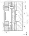
- FIG. 2 is a cross-sectional view schematically showing the structure of the resonator according to the first embodiment.
- FIG. 2 is a cross-sectional view of the resonator 1 shown in FIG. 1 along line II-II.
- the resonator 15 is held between the lower lid 20 and the upper lid 30. Specifically, the holding portion 140 of the resonator 15 is joined to the sidewall 23 of the lower lid 20 and the sidewall 33 of the upper lid 30, respectively. Thus, the lower lid 20, the upper lid 30, and the holding portion 140 form a vibration space in which the vibrating portion 110 can vibrate.
- the resonator 15, the lower lid 20, and the upper lid 30 are each formed using a silicon (Si) substrate as an example.
- the resonator 15, the lower lid 20, and the upper lid 30 may each be formed using an SOI (Silicon On Insulator) substrate in which a silicon layer and a silicon oxide film are laminated.
- the resonator 15, the lower cover 20 and the upper cover 30 are each made of a substrate other than a silicon substrate, such as a compound semiconductor substrate, a glass substrate, a ceramic substrate, a resin substrate, etc., as long as it is a substrate that can be processed by microfabrication technology. may be formed using
- a concave portion 16 is formed on the lower lid 20 side of the vibrating portion 110 .
- the recess 16 is a rectangular parallelepiped opening that opens downward.
- the upper lid 30 side of the vibrating portion 110 is substantially flat.
- the vibrating portion 110 includes a thin portion 111 corresponding to the bottom of the recess 16 and a thick portion 112 corresponding to the sidewall of the recess 16 .
- the thickness of the thick portion 112 in the Z-axis direction (hereinafter simply referred to as “thickness”) is greater than the thickness of the thin portion 111 .
- the thickness of the thick portion 112 is substantially equal to the thickness of the support portion 150 and substantially equal to the thickness of the holding portion 140 .
- the thin portion 111 corresponds to an example of the "first portion” according to the present invention
- the thick portion 112 corresponds to an example of the "second portion” according to the present invention.
- the depth of the concave portion 16 corresponds to the difference between the thickness of the thick portion 112 and the thickness of the thin portion 111 .
- the depth of the recess 16 is greater than the thickness of the silicon oxide film F21, which will be described later, and smaller than the thickness of the silicon substrate F2, which will be described later.
- the depth of the recess 16 is, for example, greater than the thickness of each of a metal film E1, a metal film E2, and a piezoelectric film F3, which will be described later, and greater than the sum of these thicknesses.
- the thin portion 111 is located between the first support arm 151A and the second support arm 151B in the Y-axis direction (hereinafter referred to as “central region”). It is provided so that the direction is the longitudinal direction.
- a central region between the first support arm 151A and the second support arm 151B is a region in which displacement is small when the vibrating section 110 vibrates in a widening manner. Therefore, it can be said that the thin portion 111 is provided in a region of the vibrating portion 110 where the displacement is small.
- a plane of the thin portion 111 when viewed from above (hereinafter referred to as a “planar shape”) is, for example, a rectangular shape.
- the thick portions 112 are provided in regions (hereinafter referred to as "outer end regions") that sandwich the central region from both directions of the X axis.
- the outer end region is a region in which displacement is large when the vibrating portion 110 vibrates in a widening manner.
- the thick portion 112 is also provided between the thin portion 111 and the support portion 150 . That is, the first support arm 151A and the second support arm 151B are connected to the thick portion 112 of the vibrating portion 110 .
- the thick portion 112 is provided in a frame shape surrounding the thin portion 111 . Also, the area of the thick portion 112 is larger than the area of the thin portion 111 .
- the number, shape, position, etc. of the thin portions are not limited to the above.
- a plurality of thin portions may be provided, and may have a polygonal shape, a circular shape, an elliptical shape, or a planar shape combining these.
- the vibrating portion 110, the holding portion 140 and the supporting portion 150 included in the resonator 15 are integrally formed by the same process.
- the resonator 15 has a silicon oxide film F21, a silicon substrate F2, a metal film E1, a piezoelectric film F3, a metal film E2, and a protective film F5.
- the resonator 15 is formed by patterning a layered body including a silicon oxide film F21, a silicon substrate F2, a metal film E1, a piezoelectric film F3, a metal film E2, a protective film F5, etc., by removal processing.
- the removing process is, for example, dry etching using an argon (Ar) ion beam.
- the concave portion 16 of the vibrating portion 110 is formed by removal processing such as dry etching, as in the patterning described above.
- the formation of the recesses 16 may be performed before the patterning described above, or may be performed after the patterning described above.
- the silicon oxide film F21 is provided on part of the lower surface of the silicon substrate F2. Specifically, they are provided on the lower surfaces of the thick portion 112 of the vibrating portion 110 , the support portion 150 and the holding portion 140 . Silicon oxide film F21 is sandwiched between silicon substrate P10 and silicon substrate F2.
- the silicon oxide film F21 is made of silicon oxide containing SiO 2 or the like, for example.
- the silicon oxide film F21 functions as a temperature characteristic correction film that reduces the temperature coefficient of the resonance frequency of the resonator 15, that is, the rate of change of the resonance frequency per unit temperature, at least around room temperature. Therefore, the silicon oxide film F21 improves the temperature characteristics of the resonator 15.
- the silicon oxide film may be formed on the upper surface of the silicon substrate F2.
- the silicon oxide film F21 corresponds to an example of the "temperature characteristic correction film" according to the present invention.
- the silicon substrate F2 is formed of, for example, a degenerate n-type silicon (Si) semiconductor with a thickness of about 6 ⁇ m.
- the silicon substrate F2 may contain phosphorus (P), arsenic (As), antimony (Sb), etc. as an n-type dopant.
- the resistance value of degenerate silicon (Si) used for the silicon substrate F2 is, for example, less than 16 m ⁇ cm, and more preferably 1.2 m ⁇ cm or less.
- the silicon semiconductor forming the silicon substrate F2 may be in any state of single crystal, polycrystal and amorphous.
- the silicon substrate F2 corresponds to an example of the "substrate" according to the invention.
- a concave portion 16 is formed in the silicon substrate F2.
- the silicon substrate F2 forms the bottom surface of the recess 16, and the silicon oxide film F21 and the silicon substrate F2 form the side surfaces of the recess 16.
- the thickness of the silicon substrate F2 at the thin portion 111 is smaller than the thickness of the silicon substrate F2 at the thick portion 112 . That is, the vibrating portion 110 is configured such that the thin portion 111 and the thick portion 112 form a recess on the side of the silicon substrate F2 opposite to the piezoelectric film F3.
- the metal film E1 is laminated on the silicon substrate F2, the piezoelectric film F3 is laminated on the metal film E1, and the metal film E2 is laminated on the piezoelectric film F3. That is, the metal film E1, the metal film E2, and the piezoelectric film F3 are provided on the side opposite to the side of the silicon substrate F2 on which the concave portions 16 are formed.
- Each of the metal film E1 and the metal film E2 has a portion that functions as an excitation electrode that excites the vibrating portion 110 and a portion that functions as an extraction electrode that electrically connects the excitation electrode to an external power supply.
- the piezoelectric film F3 corresponds to an example of the "piezoelectric layer" according to the invention.
- the metal film E1 corresponds to an example of the "lower electrode” according to the invention.
- the metal film E2 corresponds to an example of the "upper electrode” according to the invention.
- each of the metal film E1 and the metal film E2 is, for example, about 0.1 ⁇ m or more and 0.2 ⁇ m or less.
- the metal film E1 and the metal film E2 are patterned into excitation electrodes, extraction electrodes, and the like by removal processing such as etching.
- the metal film E1 and the metal film E2 are formed of, for example, a metal material having a body-centered cubic crystal structure. Specifically, the metal film E1 and the metal film E2 are formed of Mo (molybdenum), tungsten (W), or the like.
- Mo mobdenum
- W tungsten
- an insulating film may be provided between the metal film E1 and the silicon substrate F2 from the viewpoint of suppressing the generation of parasitic capacitance and the generation of a short circuit at the end of the resonator 1.
- FIG. Such an insulating film may be made of the same material as the silicon oxide film F21, or may be made of the same material as the piezoelectric film F3.
- the piezoelectric film F3 is a thin film formed of a piezoelectric material that mutually converts electrical energy and mechanical energy.
- the piezoelectric film F3 expands and contracts in the X-axis direction among the in-plane directions of the XY plane according to the electric field applied by the metal films E1 and E2. Due to the expansion and contraction of the piezoelectric film F3, the vibrating portion 110 undergoes expansion and contraction vibration in the in-plane direction.
- the piezoelectric film F3 is made of a material having a wurtzite hexagonal crystal structure, such as aluminum nitride (AlN), scandium aluminum nitride (ScAlN), zinc oxide (ZnO), gallium nitride (GaN), It can be based on a nitride or oxide such as indium nitride (InN).
- AlN aluminum nitride
- ScAlN scandium aluminum nitride
- ZnO zinc oxide
- GaN gallium nitride
- It can be based on a nitride or oxide such as indium nitride (InN).
- scandium aluminum nitride is obtained by substituting a part of aluminum in aluminum nitride with scandium, and instead of scandium, magnesium (Mg) and niobium (Nb), or magnesium (Mg) and zirconium (Zr) , may be substituted with two elements such as
- the thickness of the piezoelectric film F3 is, for example, about 1 ⁇ m, but may be about 0.2 ⁇ m to 2 ⁇ m.
- the protective film F5 is laminated on the metal film E2.
- the protective film F5 protects, for example, the metal film E2 from oxidation.
- the material of the protective film F5 is, for example, an oxide, nitride, or oxynitride containing aluminum (Al), silicon (Si), or tantalum (Ta).
- a parasitic capacitance reducing film that reduces the parasitic capacitance formed between the internal wirings of the resonator 15 may be laminated on the protective film F5.
- the thickness of the protective film F5 is sufficiently larger than the respective thicknesses of the metal film E1, the metal film E2 and the piezoelectric film F3.
- the protective film F5 reduces the appearance of irregularities caused by the respective shapes of the metal film E1, the metal film E2, and the piezoelectric film F3 on the upper surface of the vibrating portion 110, and makes the upper surface of the vibrating portion 110 closer to a flat surface. .
- a frequency adjustment film may be provided on the protective film F5 to change the mass of the vibrating portion 110 by removal processing and change the frequency of the vibrating portion 110 accordingly.
- the frequency adjustment film is, for example, a metal material such as molybdenum (Mo), tungsten (W), gold (Au), platinum (Pt), nickel (Ni) or titanium (Ti).
- a lead wire C1 and a lead wire C2 are formed on the protective film F5 of the holding portion 140 .
- the lead wiring C1 is electrically connected to the metal film E1 through through holes formed in the piezoelectric film F3 and the protective film F5.
- the lead wiring C2 is electrically connected to the metal film E2 through a through hole formed in the protective film F5.
- the lead wiring C1 and the lead wiring C2 are made of a metal material such as aluminum (Al), germanium (Ge), gold (Au), tin (Sn), or the like.
- the bottom plate 22 and side walls 23 of the lower lid 20 are integrally formed of the silicon substrate P10.
- the silicon substrate P10 is made of a non-degenerate silicon semiconductor and has a resistivity of, for example, 10 ⁇ cm or more.
- the thickness of the lower lid 20 is greater than the thickness of the silicon substrate F2, and is, for example, about 150 ⁇ m.
- the silicon substrate P10 of the lower cover 20 corresponds to the support substrate (handle layer) of the SOI substrate
- the silicon oxide film F21 of the resonator 15 corresponds to the SOI substrate. It corresponds to the BOX layer
- the silicon substrate F2 of the resonator 15 corresponds to the active layer (device layer) of the SOI substrate.
- the bottom plate 32 and side walls 33 of the upper lid 30 are integrally formed by the silicon substrate Q10.
- a silicon oxide film Q11 is provided on the surface of the silicon substrate Q10. Specifically, the region between the silicon substrate Q10 and the through electrodes V1 and V2 described later, the region between the silicon substrate Q10 and the internal terminals Y1 and Y2 described later, and the silicon substrate Q10 and the external terminal T1 described later. , T2.
- the silicon oxide film Q11 prevents short-circuiting of the electrodes through the silicon substrate Q10.
- the inner wall of the cavity 31 is not provided with an electrode or the like that causes a short circuit, so the silicon substrate Q10 may be exposed on the inner wall of the cavity 31.
- the silicon oxide film Q11 is formed, for example, by thermal oxidation of the silicon substrate Q10 or chemical vapor deposition (CVD).
- the thickness of the upper lid 30 is, for example, about 150 ⁇ m.
- a metal film 70 is provided on the lower surface of the bottom plate 32 of the upper lid 30 .
- the metal film 70 is a getter that absorbs gas in the vibrating space formed by the cavities 21 and 31 to improve the degree of vacuum.
- the metal film 70 absorbs hydrogen gas, for example.
- the metal film 70 contains, for example, titanium (Ti), zirconium (Zr), vanadium (V), niobium (Nb), tantalum (Ta), or an alloy containing at least one of these.
- the metal film 70 may include an alkali metal oxide or an alkaline earth metal oxide.
- a layer for preventing diffusion of hydrogen from the silicon substrate Q10 to the metal film 70 for example, a layer for improving adhesion between the silicon substrate Q10 and the metal film 70, etc. Layers not shown may also be provided.
- the upper cover 30 is provided with through electrodes V1 and through electrodes V2.
- the through-electrodes V1 and V2 are provided inside through-holes that penetrate the side wall 33 in the Z-axis direction.
- the through electrodes V1 and V2 are surrounded by a silicon oxide film Q11 and insulated from each other.
- the through electrodes V1 and V2 are formed by, for example, filling through holes with polycrystalline silicon (Poly-Si), copper (Cu), gold (Au), or the like.
- An internal terminal Y1 and an internal terminal Y2 are provided on the lower surface of the upper lid 30, and an external terminal T1 and an external terminal T2 are provided on the upper surface of the upper lid 30.
- the internal terminal Y1 is connected to the lower end of the through electrode V1, and the external terminal T1 is connected to the upper end of the through electrode V1.
- the internal terminal Y2 is connected to the lower end of the through electrode V2, and the external terminal T2 is connected to the upper end of the through electrode V2.
- the internal terminal Y1 is a connection terminal that electrically connects the through electrode V1 and the lead wire C1
- the external terminal T1 is a mounting terminal that grounds the metal film E1.
- the internal terminal Y2 is a connection terminal that electrically connects the through electrode V2 and the lead wire C2, and the external terminal T2 is a mounting terminal that electrically connects the metal film E2 to an external power supply.
- the internal terminals Y1 and Y2 are electrically insulated from each other by a silicon oxide film Q11.
- a plurality of external terminals including external terminals T1 and T2 are also electrically insulated from each other by silicon oxide film Q11.
- the internal terminals Y1, Y2 and the external terminals T1, T2 are, for example, metallized layers (base layers) such as chromium (Cr), tungsten (W), nickel (Ni), nickel (Ni), gold (Au), and silver. (Ag), copper (Cu), or the like is plated.
- a joint portion H is formed between the side wall 33 of the upper lid 30 and the holding portion 140 of the resonator 15 .
- the joint H is provided in a frame shape that is continuous in the circumferential direction so as to surround the vibrating portion 110 when viewed from above, and hermetically seals the vibrating space formed by the cavities 21 and 31 in a vacuum state.
- the junction H is formed of, for example, a metal film in which an aluminum (Al) film, a germanium (Ge) film, and an aluminum (Al) film are laminated in this order from the resonator 15 side and eutectic bonded.
- the junction H is made of gold (Au), tin (Sn), copper (Cu), titanium (Ti), aluminum (Al), germanium (Ge), titanium (Ti), silicon (Si), and at least one of these. It may also include alloys containing species.
- the junction H may contain an insulator made of a metal compound such as titanium nitride (TiN) or tantalum nitride (TaN).
- TiN titanium nitride
- TaN tantalum nitride
- the vibrating portion 110 has a concave shape on the opposite side of the silicon substrate F2 to the piezoelectric film F3 that vibrates in a wide-spreading manner.
- the vibrating portion 110 has a thin portion 111 corresponding to the bottom of the recess 16 and a thick portion 112 corresponding to the sidewall of the recess 16 .
- Thick portion 112 is thicker than thin portion 111 .
- flexural vibration bending in the Z-axis direction may also occur due to the asymmetry of the laminated structure in the Z-axis direction.
- the bending vibration vibrates the supporting portion 150 and leaks vibrational energy to the holding portion 140, which may cause a decrease in vibration confinement.
- the concave portion 16 by providing the concave portion 16, it is possible to control the vibration mode and suppress unnecessary vibration such as the bending vibration. Therefore, according to this embodiment, it is possible to provide the resonator 15 with high vibration confinement and the resonator 1 including the same.
- the recess 16 is provided on the lower lid 20 side of the vibrating portion 110, and the upper lid 30 side surface of the silicon substrate F2 of the vibrating portion 110 on which the excitation electrodes and the like are provided is made flatter than the lower lid 20 side surface. , it is possible to suppress machining defects such as step disconnection and short circuit of the excitation electrode.
- the area of the thin portion 111 is smaller than the area of the thick portion 112 in plan view, the reduction in the mechanical strength of the vibrating portion 110 due to the formation of the concave portion 16 is suppressed. Therefore, damage to the resonator 15 due to impact during manufacturing or transportation can be suppressed, and reliability can be improved.
- a silicon oxide film F21 is provided on the lower lid 20 side of the silicon substrate F2.
- the silicon oxide film F21 corrects the frequency-temperature characteristic of the silicon substrate F2, thereby improving the frequency-temperature characteristic.
- the silicon oxide film F21 is provided on the thick portion 112 and is not provided on the inner wall of the recess 16 .
- the manufacturing process of the resonator 15 can be simplified. Further, even if a portion of the silicon oxide film F21 is removed when forming the thin portion 111 as described above, the area of the thin portion 111 is smaller than the area of the thick portion 112, so the silicon oxide film F21 is partially removed. It is possible to suppress the influence on the frequency temperature characteristics due to the fact that
- the silicon substrate F2 is adopted as the “substrate” according to the present invention
- the silicon oxide film F21 is adopted as the "temperature characteristic correction film” according to the present invention.
- the frequency temperature characteristic can be corrected easily and inexpensively.
- the thin portion 111 is provided in a central region sandwiched between the first support arm 151A and the second support arm 151B.
- the thin portion 111 in the central region where the displacement during vibration is small and the frequency-temperature characteristics are less likely to be affected, it is possible to achieve both good frequency-temperature characteristics and high vibration confinement properties. can be done.
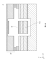
- FIG. 3 is a cross-sectional view schematically showing the structure of the resonator according to the second embodiment.
- This embodiment differs from the first embodiment in that the thickness of the first support arm 251A and the second support arm 251B of the support portion 250 is reduced. Specifically, the thickness of the first support arm 251A is smaller than the thickness of the thick portion 112 . As shown in FIG. 3 , the thickness of the first support arm 251A is smaller than the thickness of the thin portion 111 . Also, the thickness of the first support arm 251A is smaller than the thickness of the holding portion 140 . Such a thickness relationship also applies to the second support arm 251B. However, the thickness of the first support arm 251A may be larger than the thickness of the thin portion 111 as long as it is smaller than the thickness of the thick portion 112, and may be equal to or greater than the thickness of the holding portion 140. .
- the thickness of the first support arm 251A is, for example, approximately equal to the thickness of the second support arm 251B, but may be larger or smaller than the thickness of the second support arm 251B.
- the silicon oxide film F21 is not provided on the surface of the support portion 250 on the lower lid 20 side, and the silicon substrate F2 is exposed.
- a silicon oxide film may be provided on the surface of the support portion 250 on the lower lid 20 side.
- Such a support portion 250 can be formed, for example, by etching from the lower lid 20 side. By making the thickness of the support portion 250 smaller than the thickness of the thick portion 112 to which the support portion 250 is connected in this manner, leakage of vibration from the vibrating portion 110 to the holding portion 140 via the support portion 250 is suppressed. be able to.
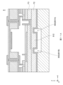
- FIG. 4 is a cross-sectional view schematically showing the structure of the resonator according to the third embodiment.
- the thickness of the first support arm 351A and the second support arm 351B of the support portion 350 is substantially the same as the thickness of the thin portion 111 .
- the silicon oxide film F21 is not provided on the surface of the support portion 350 on the lower lid 20 side, similarly to the surface of the thin portion 111 on the lower lid 20 side, and the silicon substrate F2 is exposed. According to this, in the manufacturing process of the resonance device 3, the manufacturing process can be simplified by collectively performing the etching processing of the supporting portion 350 and the thin portion 111. FIG. If the thickness of the support portion 350 and the thickness of the thin portion 111 are the same, a silicon oxide film F21 may be provided on the surfaces of the support portion 350 and the thin portion 111 on the lower lid 20 side.
- FIG. 5 is a cross-sectional view schematically showing the structure of the resonator according to the fourth embodiment.
- the thickness of the holding portion 440 is smaller than the thickness of the thick portion 112 .
- the thickness of the holding portion 440 is approximately the same as the thickness of the support portion 450 and approximately the same as the thickness of the thin portion 111 .
- the surface of the first support arm 451A on the lower lid 20 side and the surface of the first frame portion 441A on the lower lid 20 side are substantially flush with each other. These contents are the same for the second support portion 451B and the second frame portion 441B.
- the silicon oxide film F21 is not provided on the surfaces of the holding portion 440 and the support portion 450 on the lower lid 20 side, and the silicon substrate F2 is exposed.
- a silicon oxide film may be provided on the surfaces of the holding portion 440 and the support portion 450 on the lower lid 20 side.
- the resonance device 4 can be miniaturized.
- the support portion 450 is formed to have the same thickness as the thin portion 111 and the holding portion 440, the etching processing of the support portion 450, the thin portion 111 and the holding portion 440 in the manufacturing process of the resonance device 4 can be eliminated. By collectively performing the treatment, the manufacturing process can be simplified.
- the holding portion 440 may be formed to have a thickness different from that of the thin portion 111 and the support portion 450 .
- the thickness of the holding portion 440 is substantially equal to the thickness of the thick portion 112. Thickness can be reduced.
- the etching processing of the holding portion 440 and the supporting portion 450 can be performed collectively. The same applies to the case where the thicknesses of the thin portion 111 and the holding portion 440 are substantially the same and different from the thickness of the support portion 450 .
- FIG. 6 is a cross-sectional view schematically showing the structure of the resonator according to the fifth embodiment.
- the silicon oxide film F21 is provided not only on the lower surface of the thick portion 512 of the vibrating portion 510, but also on the lower surface of the thin portion 511, that is, on the bottom surface of the concave portion 56 of the vibrating portion 510.
- the silicon oxide film F21 is provided on the lower lid 20 side of the silicon substrate F2 and on the surface of the vibrating portion 510 in the direction along the main surface of the silicon substrate F2. According to this, better frequency temperature characteristics can be obtained.
- the silicon oxide film F21 is not provided on the side surface of the recess 56. As shown in FIG. Therefore, inhibition of vibration by the silicon oxide film is reduced compared to the structure in which the silicon oxide film is continuously provided over the thick portion and the thin portion.
- the silicon oxide film F21 is provided on the entire bottom surface of the thin portion 511 in the example shown in FIG. Moreover, the silicon oxide film F21 may be provided on a part of the side surface of the recess 56 as long as the silicon oxide film F21 is discontinuous at the boundary between the thick portion 512 and the thin portion 511 .
- FIG. 7 is a cross-sectional view schematically showing the structure of the resonator according to the sixth embodiment.
- the silicon oxide film F21 is provided not only on the lower surface of the thick portion 612 of the vibrating portion 610 but also on the lower surface of the thin portion 611, and the silicon oxide film F21 is continuous over the thick portion 612 and the thin portion 611. is provided.
- the silicon oxide film F21 is also provided on the side surface of the concave portion 66 of the vibrating portion 610 . In other words, it is provided on the lower cover 20 side of the silicon substrate F2 and on the surface of the vibrating portion 610 in the direction along the main surface of the silicon substrate F2 and in the direction intersecting the main surface. That is, the silicon oxide film F21 is provided on the entire surface of the vibrating portion 610 on the lower lid 20 side. Therefore, in the manufacturing process, the silicon oxide film F21 can be formed after the recess 66 is formed, and the manufacturing cost can be reduced as compared with the fifth embodiment.
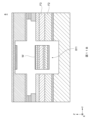
- FIG. 8 is a plan view schematically showing the structure of a resonator according to the seventh embodiment.
- 9A, 9B and 9C are cross-sectional views taken along lines IXA-IXA, IXB-IXB and IXC-IXC of FIG.
- the thin portion 711 is formed in a central region of the vibrating portion 710 sandwiched between the first support arm 751A and the second support arm 751B of the support portion 750 in the Y-axis direction. to the second support arm 751B, and the first support arm 751A and the second support arm 751B are connected to the thin portion 711.
- the thick portions 712 are provided in outer end regions that sandwich the central region from both directions of the X axis.
- the width of the thin portion 711 in the X-axis direction is substantially equal to the width of each of the first support arm 751A and the second support arm 751B in the X-axis direction.
- the recesses 76 are provided in substantially the entire central region where the displacement due to vibration is smaller than that in the outer end region. According to this, compared to a configuration in which a recess is provided in a part of the central region in the Y-axis direction, the recess can be made larger while suppressing the influence on the vibration characteristics, so that the vibration confinement property can be improved. can.
- the thickness of the support portion 750 is smaller than the thickness of the thick portion 712 and the holding portion 740, for example. Since the thickness changes at the boundary between the support portion 750 and the holding portion 740, vibration leakage from the support portion 750 to the holding portion 740 can be suppressed. Therefore, it is possible to improve the confinement of vibration.
- the thickness of the support portion 750 is, for example, substantially the same as the thickness of the thin portion 711, but is not limited to this.
- the thickness of the support portion 750 may be larger or smaller than the thickness of the thin portion 711 .
- the thin portion 711 has a rectangular planar shape.
- the shape is not limited to the above.
- the planar shape of the thin portion 711 may be polygonal, circular, elliptical, or a combination thereof.
- the width of the thin portion 711 in the X-axis direction is formed substantially equal to the width in the X-axis direction of the first support arm 751A and the second support arm 751B, but the width is not limited to this width.
- the width of the thin portion 711 in the X-axis direction is the width of the first support arm 751A and the second support arm 751B in the X-axis direction. may be larger or smaller than the width of
- a frequency adjustment film W is provided on the upper lid 30 side of the vibrating portion 710 .
- a frequency adjustment film W is provided in the outer end region. Since the frequency of the vibrating portion 710 that spreads and vibrates depends on the weight of the outer end region of the vibrating portion 710, the frequency can be adjusted by trimming the frequency adjustment film W.
- FIG. From the viewpoint of suppressing peeling and damage of the frequency adjustment film W due to strain during vibration of the vibrating portion 710, the frequency adjustment film W should be provided only in the outer end region, avoiding the central region where the strain during vibration is large. is preferred.
- the width of the frequency adjustment film W in the X-axis direction is preferably 5 ⁇ m or more. Therefore, the width in the X-axis direction of the outer end region where the frequency adjustment film W is provided is preferably 5 ⁇ m or more.
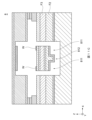
- FIG. 10 is a plan view schematically showing the structure of the resonator according to the eighth embodiment.
- 11A, 11B and 11C are cross-sectional views taken along lines XIA-XIA, XIB-XIB and XIC-XIC in FIG.
- a thick portion 812 is provided in a central region sandwiched between the first support arm 851A and the second support arm 851B of the support portion 850 in the Y-axis direction. extends in a belt shape from the first support arm 851A to the second support arm 851B, and the first support arm 851A and the second support arm 851B are connected to the thick portion 812.
- a thin portion 811 is provided in the outer end region sandwiching the central region from both directions of the X axis. That is, the vibrating portion 810 is configured such that the side of the silicon substrate F2 opposite to the piezoelectric film F3 is convex.
- the thickness of the support portion 850 is, for example, greater than the thickness of the thin portion 811 and substantially equal to the thickness of the thick portion 812 and the holding portion 840 . Since the thickness changes at the boundary between the vibrating portion 810 and the supporting portion 850, vibration leakage from the vibrating portion 810 to the supporting portion 850 can be suppressed. Moreover, since the thickness changes at the boundary between the support portion 850 and the holding portion 840, vibration leakage from the support portion 850 to the holding portion 840 can be suppressed. Therefore, it is possible to improve the confinement of vibration.
- the planar shape of the thick portion 812 is rectangular. is not limited to the above.
- the planar shape of the thick portion 812 may be polygonal, circular, elliptical, or a combination thereof.
- the width of the thick portion 812 in the X-axis direction is formed substantially equal to the width in the X-axis direction of the first support arm 851A and the second support arm 851B, but the width is not limited to this width.
- the width of the thick portion 812 in the X-axis direction is equal to the X-axis width of the first support arm 851A and the second support arm 851B. It may be larger or smaller than the width of the direction.
- the frequency of the vibrating portion 810 that spreads and vibrates depends on the weight of the outer end region of the vibrating portion 810 , the frequency can be adjusted by adjusting the thickness of the thin portion 811 .
- the thickness of the thin portion 811 is adjusted, for example, by trimming the silicon substrate F2 in the outer end region. If the thickness of the thick portion 812 in the central region changes, the frequency temperature characteristic will change, so it is preferable to trim only the outer end region while avoiding the central region. Therefore, from the viewpoint of trimming accuracy, the width of the outer end region in the X-axis direction is preferably 5 ⁇ m or more.
- the thick portion is provided in at least a part of the central region, and the first support arm and the second support arm are connected to each other. At least one may be connected to the thin portion.
- a thick portion may be provided in an intermediate portion in the Y-axis direction (hereinafter simply referred to as “intermediate portion”), and the thick portion may be provided in an island shape surrounded by thin portions in plan view.
- the frequency temperature characteristic can be adjusted by adjusting the ratio of the thick portion and the thin portion in the central region.
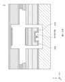
- FIG. 12 is a plan view schematically showing the structure of the resonator according to the ninth embodiment.
- 13A, 13B and 13C are cross-sectional views along lines XIIIA-XIIIA, XIIIB-XIIIB and XIIIC-XIIIC of FIG.
- a thin portion 911 is provided in the central region sandwiched between the first support arm 951A and the second support arm 951B of the support portion 950 in the Y-axis direction.
- thick portions 912 are provided in outer end regions sandwiching the central region from both directions of the X axis.
- the thin portion 911 has a wide intermediate portion. That is, as shown in FIGS. 12 and 13C, the vibrating portion 910 includes a thin portion 911A provided in the middle portion of the central region, and a thin portion 911A provided in the middle portion of the outer end region and adjacent to the central region. It has thin portions 911 B and thick portions 912 provided at the four corners of the vibrating portion 910 . According to this, it is possible to provide a resonance device having a higher vibration confinement property than that of the seventh embodiment.
- the planar shape of the intermediate portion of the thin portion 911 is rectangular, but is not limited to this.
- the planar shape of the intermediate portion of the thin portion 911 may be polygonal, circular, elliptical, or a combination thereof.
- the thickness of the thin portion 911A is substantially the same as the thickness of the thin portion 911B, but may be larger or smaller than the thickness of the thin portion 911B.
- the thin portion 911B reaches the outer end of the vibrating portion 910 on both sides of the thin portion 911A in the X-axis direction.
- the thin portion 911B does not reach the outer end of the vibrating portion 910 on both sides of the thin portion 911A in the X-axis direction, and is spaced apart from the outer end of the vibrating portion 910.
- the outer end of the intermediate portion of vibrating portion 910 may have the same thickness as thick portion 912 .
- the width of the thick portion 912 adjacent to the thin portion 911B in the X-axis direction is preferably 5 ⁇ m or more from the viewpoint of trimming accuracy.
- the width of the thick portion 912 adjacent to the thin portion 911B in the Y-axis direction is preferably 5 ⁇ m or more.
- the width of the portion other than the intermediate portion may be configured to be wide. That is, the intermediate portion of the thin portion may be configured to have a narrow width.
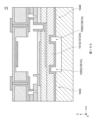
- FIG. 14 is a plan view schematically showing the structure of the resonator according to the tenth embodiment.
- 15A, 15B and 15C are cross-sectional views along lines XVA-XVA, XVB-XVB and XVC-XVC of FIG.
- a thick portion 1012 is provided in the central region sandwiched between the first support arm 1051A and the second support arm 1051B of the support portion 1050 in the Y-axis direction.
- a thin portion 1011 is provided in the outer end region sandwiching the central region from both directions of the X axis.
- the thick portion 1012 has a wide intermediate portion. That is, as shown in FIGS. 14 and 15C, the vibrating portion 1010 includes a thick portion 1012A provided in the middle portion of the central region and a portion adjacent to the central region in the middle portion of the outer end region. and thin portions 1011 provided at the four corners of the vibrating portion 910 . According to this, it is possible to provide a resonance device having a higher vibration confinement property than the eighth embodiment.
- the planar shape of the intermediate portion of the thick portion 1012 is rectangular, but is not limited to this.
- the planar shape of the intermediate portion of the thick portion 1012 may be polygonal, circular, elliptical, or a combination thereof.
- the thickness of thick portion 1012A is approximately the same as the thickness of thick portion 1012B, but may be greater or less than the thickness of thick portion 1012B.
- the width of the thick portion 1012 in the X-axis direction is formed substantially equal to the width in the X-axis direction of the first support arm 851A and the second support arm 851B, but the width is not limited to this width.
- the width of the thick portion 812 in the X-axis direction may be larger or smaller than the width of the first support arm 851A and the second support arm 851B in the X-axis direction.
- the thick portion 1012B reaches the outer end of the vibrating portion 1010 on both sides of the thick portion 1011A in the X-axis direction.
- apart from the example shown in FIG. may be provided with an opening.
- the outer end of the intermediate portion of vibrating portion 1010 may have the same thickness as thin portion 1011 .
- the width of the thin portion 1011 adjacent to the thick portion 1012B in the X-axis direction is preferably 5 ⁇ m or more from the viewpoint of trimming accuracy.
- the width of the thin portion 1011 adjacent to the thick portion 1012B in the Y-axis direction is preferably 5 ⁇ m or more.
- the thick portion is provided in at least a part of the central region, and the first support arm and the second support arm are connected to each other. At least one may be connected to the thin portion.
- a thick portion may be provided in an intermediate portion in the Y-axis direction, and the thick portion may be provided in an island shape surrounded by thin portions in plan view. In such a configuration, the frequency temperature characteristic can be adjusted by adjusting the ratio of the thick portion and the thin portion in the central region.
- the intermediate portion of the thick portion 1012 is configured to be wide, but portions other than the intermediate portion may be configured to be wide. That is, the intermediate portion of the thick portion may be configured to have a narrow width.
- FIG. 16 is a cross-sectional view schematically showing the structure of the resonator according to the eleventh embodiment.
- the resonator 60 has a first silicon layer F2A and a second silicon layer F2B, with a silicon oxide film F21 provided therebetween.
- the first silicon layer F2A is provided on the upper lid 30 side of the second silicon layer F2B.
- the first silicon layer F2A is the vibration portion 1110, the holding portion 1140 (including the first frame portion 1141A and the second frame portion 1141B), and the support portion 1150 (that is, the first support arm 1151A and the second support arm 1151B). provided throughout the area.
- the first silicon layer F2A is provided with a uniform thickness in the thin portion 1111 and the thick portion 1112 .
- the silicon oxide film F21 is similarly provided with a uniform thickness.
- the second silicon layer F2B is provided on the holding portion 1140 and the supporting portion 1150 .
- the second silicon layer F2B is provided in the thick portion 1112 avoiding the thin portion 1111 in the vibrating portion 1110 . Therefore, the silicon oxide film F21 is provided so as to be exposed on the bottom surface of the recess 116 in the thin portion 1111 of the vibrating portion 1110, and the second silicon layer F2B is provided so as to be exposed to the side surface of the recess 116.
- the thickness of the second silicon layer F2B may be greater than the thickness of the first silicon layer F2A.
- a silicon oxide film P11 is provided on the resonator 60 side of the lower lid 20 . The silicon oxide film P11 is continuously provided over the bonding surface between the silicon substrate P10 and the second silicon layer F2B and the inner surface of the cavity 21 .
- etching is stopped at the silicon oxide film F21 provided between the first silicon layer F2A and the second silicon layer F2B, thereby reducing the thickness of the thin portion 1111. It can be adjusted with high accuracy, and the frequency temperature characteristics and frequency variations can be suppressed.
- a vibrating portion 1110 shown in FIG. 16 is an example of a vibrating portion having a concave shape on the lower lid side.
- the resonator has a first silicon layer and a second silicon layer, and a silicon oxide film is provided between them
- the lower cover side of the vibrating portion may be formed in a convex shape or a concave shape other than the above.
- the vibrating portion is the seventh embodiment. It may have a planar thick portion and thin portion as in the tenth embodiment.
- a vibrating section including a substrate and a piezoelectric layer provided on the main surface of the substrate and vibrating along the main surface of the substrate in response to an applied voltage;
- a vibrating portion comprising a holding portion provided around at least a portion of the vibrating portion and a supporting portion provided between the holding portion and the vibrating portion and supporting the vibrating portion in plan view on the main surface of the substrate, has a first portion that is a part of the main surface of the substrate in plan view and a second portion that is another region in plan view of the main surface of the substrate, and intersects the main surface of the substrate.
- the thickness of the second portion in the thickness direction is larger than the thickness of the first portion in the thickness direction, and the vibrating portion is a piezoelectric body on the substrate by the first portion and the second portion.
- a resonator is provided whose side opposite the layer is configured concavely or convexly.
- the vibrating portion has a concave shape on the side of the substrate opposite to the piezoelectric layer, the first portion corresponds to the concave bottom portion of the vibrating portion, and the second portion corresponds to the concave side wall of the vibrating portion. It can correspond to the department.
- the support part may be connected to the second part, and the thickness of the support part in the thickness direction may be equal to the thickness of the second part in the thickness direction.
- the vibration mode can be controlled by the concave portion provided on the opposite side of the substrate from the piezoelectric layer, and the vibration confinement property of the resonator can be improved.
- the support part may be connected to the second part, and the thickness of the support part in the thickness direction may be smaller than the thickness of the second part in the thickness direction.
- the thickness of the supporting portion is thin, it is possible to suppress vibration leakage from the supporting portion and further improve the vibration containment property of the resonator. Also, by maintaining the thickness of the vibrating portion, it is possible to obtain good frequency-temperature characteristics.
- the thickness of the support portion in the thickness direction may be equal to the thickness of the first portion in the thickness direction.
- the supporting portion and the vibrating portion can be processed collectively, and a resonator with excellent productivity can be provided.
- the thickness of the holding portion in the thickness direction may be equal to the thickness of the support portion in the thickness direction.
- the height of the holding portion can be lowered, the height of the product can be lowered and the size can be reduced.
- the support portion has a pair of support arms provided facing each other across the vibrating portion, and the first portion is a pair of support arms in a region sandwiched between the pair of support arms in the vibrating portion.
- the support may extend in a strip shape from one end to the other end of the support, and the support may be connected to the first portion.
- the first portion and the second portion of the vibrating portion have different thicknesses, it is possible to control the vibration mode and further improve the confinement of vibration.
- the first portion may be configured such that the intermediate portion of the band-like extending region of the first portion is wide.
- the confinement of vibration can be improved by the concave portion provided in the intermediate portion.
- the vibrating portion has a convex shape on the side of the substrate opposite to the piezoelectric layer, the second portion corresponds to the convex top portion of the vibrating portion, and the first portion corresponds to the convex portion of the vibrating portion. It may correspond to a shaped side wall portion.
- the support portion has a pair of support arms provided facing each other across the vibrating portion, and the second portion is a pair of support arms in a region sandwiched between the pair of support arms in the vibrating portion. may extend from one end to the other end in a strip shape, and the support portion may be connected to the second portion.
- good frequency temperature characteristics can be obtained by optimizing the thickness of the central portion of the vibrator sandwiched between the support arms.
- the second portion may be configured such that the intermediate portion of the band-like extending region of the second portion is wide.
- the confinement of vibration can be improved by the concave portion provided in the intermediate portion.
- the vibrating section may have a temperature characteristic correction film that corrects the temperature characteristic of the substrate, and the temperature characteristic correction film may be provided on at least a portion of the substrate opposite to the piezoelectric layer.
- the temperature characteristic correction film may be provided on the surface of the vibrating portion in the direction along the main surface of the substrate.
- the temperature characteristic correction film is formed on the vibrating portion, the temperature characteristic correction film is not formed on the surface of the piezoelectric layer and the vibration is not hindered. Frequency temperature characteristics can be obtained.
- the temperature characteristic correction film may be further provided on a surface of the vibrating portion in a direction intersecting the main surface of the substrate.
- the temperature characteristic correction film can be collectively formed by thermal oxidation after film formation.
- the substrate is a silicon substrate
- the temperature characteristic correction film is a silicon oxide film
- the substrate includes a first silicon substrate, a silicon oxide film provided on the side of the first silicon substrate opposite to the piezoelectric layer, and a second silicon oxide film provided on the side of the silicon oxide film opposite to the piezoelectric layer. 2 silicon substrates, and the silicon oxide film is exposed on the side opposite to the piezoelectric layer in the first portion.
- the thickness can be adjusted with high precision, and variations in frequency temperature characteristics and frequency can be suppressed.
- a resonator a lower cover joined to a holding part, and an upper cover joined to the holding part and forming an internal space between the lower cover and the lower cover for accommodating the vibrating part, A resonator device is provided.
- Embodiments according to the present invention are applicable without particular limitation to devices that utilize the frequency characteristics of a vibrator, such as timing devices, sound generators, oscillators, and load sensors.
Landscapes
- Physics & Mathematics (AREA)
- Acoustics & Sound (AREA)
- Piezo-Electric Or Mechanical Vibrators, Or Delay Or Filter Circuits (AREA)
Priority Applications (3)
| Application Number | Priority Date | Filing Date | Title |
|---|---|---|---|
| CN202280081086.8A CN118451653A (zh) | 2021-12-06 | 2022-07-28 | 谐振器以及谐振装置 |
| JP2023566084A JP7685163B2 (ja) | 2021-12-06 | 2022-07-28 | 共振子及び共振装置 |
| US18/669,835 US20240305266A1 (en) | 2021-12-06 | 2024-05-21 | Resonator and resonance device |
Applications Claiming Priority (2)
| Application Number | Priority Date | Filing Date | Title |
|---|---|---|---|
| JP2021197531 | 2021-12-06 | ||
| JP2021-197531 | 2021-12-06 |
Related Child Applications (1)
| Application Number | Title | Priority Date | Filing Date |
|---|---|---|---|
| US18/669,835 Continuation US20240305266A1 (en) | 2021-12-06 | 2024-05-21 | Resonator and resonance device |
Publications (1)
| Publication Number | Publication Date |
|---|---|
| WO2023105845A1 true WO2023105845A1 (ja) | 2023-06-15 |
Family
ID=86730070
Family Applications (1)
| Application Number | Title | Priority Date | Filing Date |
|---|---|---|---|
| PCT/JP2022/029124 Ceased WO2023105845A1 (ja) | 2021-12-06 | 2022-07-28 | 共振子及び共振装置 |
Country Status (4)
| Country | Link |
|---|---|
| US (1) | US20240305266A1 (https=) |
| JP (1) | JP7685163B2 (https=) |
| CN (1) | CN118451653A (https=) |
| WO (1) | WO2023105845A1 (https=) |
Citations (4)
| Publication number | Priority date | Publication date | Assignee | Title |
|---|---|---|---|---|
| WO2016063863A1 (ja) * | 2014-10-22 | 2016-04-28 | 株式会社村田製作所 | 共振子及び共振装置 |
| WO2019008830A1 (ja) * | 2017-07-05 | 2019-01-10 | 株式会社村田製作所 | 共振子及び共振装置 |
| WO2020213210A1 (ja) * | 2019-04-19 | 2020-10-22 | 株式会社村田製作所 | 共振子及び共振装置 |
| JP2021513774A (ja) * | 2018-02-08 | 2021-05-27 | キョーセラ ティキティン オーユーKyocera Tikitin Oy | Mems共振器の構成 |
-
2022
- 2022-07-28 JP JP2023566084A patent/JP7685163B2/ja active Active
- 2022-07-28 CN CN202280081086.8A patent/CN118451653A/zh active Pending
- 2022-07-28 WO PCT/JP2022/029124 patent/WO2023105845A1/ja not_active Ceased
-
2024
- 2024-05-21 US US18/669,835 patent/US20240305266A1/en active Pending
Patent Citations (4)
| Publication number | Priority date | Publication date | Assignee | Title |
|---|---|---|---|---|
| WO2016063863A1 (ja) * | 2014-10-22 | 2016-04-28 | 株式会社村田製作所 | 共振子及び共振装置 |
| WO2019008830A1 (ja) * | 2017-07-05 | 2019-01-10 | 株式会社村田製作所 | 共振子及び共振装置 |
| JP2021513774A (ja) * | 2018-02-08 | 2021-05-27 | キョーセラ ティキティン オーユーKyocera Tikitin Oy | Mems共振器の構成 |
| WO2020213210A1 (ja) * | 2019-04-19 | 2020-10-22 | 株式会社村田製作所 | 共振子及び共振装置 |
Also Published As
| Publication number | Publication date |
|---|---|
| JP7685163B2 (ja) | 2025-05-29 |
| US20240305266A1 (en) | 2024-09-12 |
| JPWO2023105845A1 (https=) | 2023-06-15 |
| CN118451653A (zh) | 2024-08-06 |
Similar Documents
| Publication | Publication Date | Title |
|---|---|---|
| US20200290865A1 (en) | Mems device | |
| US11753296B2 (en) | MEMS device and method for manufacturing mems device | |
| US10879873B2 (en) | Resonator and resonance device | |
| US12552662B2 (en) | Package structure and method for manufacturing the same | |
| US11990890B2 (en) | Resonator and resonance device including same | |
| US20240333249A1 (en) | Resonator and resonating device | |
| JP7482402B2 (ja) | 共振子及び共振装置 | |
| JP6015010B2 (ja) | 振動素子、振動子、発振器および電子機器 | |
| CN112703672B (zh) | 谐振子以及谐振装置 | |
| US12107564B2 (en) | Resonator and resonance device including the same | |
| JP7685163B2 (ja) | 共振子及び共振装置 | |
| JP7591182B2 (ja) | 共振装置及びその製造方法 | |
| CN116601870A (zh) | 谐振子以及谐振装置 | |
| CN115398802A (zh) | 谐振子以及谐振装置 | |
| US12494763B2 (en) | Resonance device | |
| WO2023007787A1 (ja) | 共振装置及びその製造方法 | |
| US20250337386A1 (en) | Resonance device and method for manufacturing same | |
| US20240380380A1 (en) | Resonator, resonance device, and method for manufacturing resonator | |
| WO2025253683A1 (ja) | 共振装置及びその製造方法 | |
| US20240039511A1 (en) | Vibrator And Vibrator Device | |
| WO2022163020A1 (ja) | 共振装置及びその製造方法 | |
| JP2017005757A (ja) | 振動素子、振動子、発振器および電子機器 |
Legal Events
| Date | Code | Title | Description |
|---|---|---|---|
| 121 | Ep: the epo has been informed by wipo that ep was designated in this application |
Ref document number: 22903781 Country of ref document: EP Kind code of ref document: A1 |
|
| ENP | Entry into the national phase |
Ref document number: 2023566084 Country of ref document: JP Kind code of ref document: A |
|
| WWE | Wipo information: entry into national phase |
Ref document number: 202280081086.8 Country of ref document: CN |
|
| NENP | Non-entry into the national phase |
Ref country code: DE |
|
| 122 | Ep: pct application non-entry in european phase |
Ref document number: 22903781 Country of ref document: EP Kind code of ref document: A1 |