WO2023100285A1 - 加算回路 - Google Patents
加算回路 Download PDFInfo
- Publication number
- WO2023100285A1 WO2023100285A1 PCT/JP2021/044064 JP2021044064W WO2023100285A1 WO 2023100285 A1 WO2023100285 A1 WO 2023100285A1 JP 2021044064 W JP2021044064 W JP 2021044064W WO 2023100285 A1 WO2023100285 A1 WO 2023100285A1
- Authority
- WO
- WIPO (PCT)
- Prior art keywords
- resistor
- input terminal
- operational amplifier
- resistors
- adder circuit
- Prior art date
- Legal status (The legal status is an assumption and is not a legal conclusion. Google has not performed a legal analysis and makes no representation as to the accuracy of the status listed.)
- Ceased
Links
Images
Classifications
-
- H—ELECTRICITY
- H03—ELECTRONIC CIRCUITRY
- H03F—AMPLIFIERS
- H03F3/00—Amplifiers with only discharge tubes or only semiconductor devices as amplifying elements
- H03F3/45—Differential amplifiers
-
- H—ELECTRICITY
- H03—ELECTRONIC CIRCUITRY
- H03F—AMPLIFIERS
- H03F3/00—Amplifiers with only discharge tubes or only semiconductor devices as amplifying elements
- H03F3/60—Amplifiers in which coupling networks have distributed constants, e.g. with waveguide resonators
-
- G—PHYSICS
- G06—COMPUTING OR CALCULATING; COUNTING
- G06F—ELECTRIC DIGITAL DATA PROCESSING
- G06F7/00—Methods or arrangements for processing data by operating upon the order or content of the data handled
- G06F7/06—Arrangements for sorting, selecting, merging, or comparing data on individual record carriers
- G06F7/14—Merging, i.e. combining at least two sets of record carriers each arranged in the same ordered sequence to produce a single set having the same ordered sequence
-
- H—ELECTRICITY
- H03—ELECTRONIC CIRCUITRY
- H03F—AMPLIFIERS
- H03F3/00—Amplifiers with only discharge tubes or only semiconductor devices as amplifying elements
- H03F3/20—Power amplifiers, e.g. Class B amplifiers, Class C amplifiers
Definitions
- This disclosure relates to an adder circuit.
- N is an integer of 2 or more.
- the summing circuit includes N summing input resistors and an operational amplifier. A signal to be added is applied to one end of each addition input resistor. The other end of each addition input resistor is connected to the inverting input terminal of the operational amplifier. A non-inverting input terminal of the operational amplifier is connected to the ground.
- the parasitic capacitance of the line connecting the addition input resistor and the inverting input terminal of the operational amplifier increases as the length of the line increases.
- the adder circuit disclosed in Patent Document 1 not all of the N adder input resistors can be arranged near the operational amplifier. As the number of signals to be added increases, the number of summing input resistors also increases. As a result, it becomes difficult to arrange the summing input resistors close to the operational amplifier, so the number of summing input resistors with large parasitic capacitance increases. Since the adder circuit has an adder input resistor with a large parasitic capacitance, there is a problem that the flatness of the frequency characteristic of the pass gain in the adder circuit may be degraded.
- An object of the present invention is to obtain an adder circuit capable of preventing deterioration of flatness of frequency characteristics.
- the adding circuit includes a plurality of first resistors to which a signal to be added is applied at one end, a plurality of transmission lines to which the other end and one end of each of the first resistors are connected, and a plurality of transmission lines. It comprises a second resistor whose one end is connected to all the other ends of the line, and an amplifier circuit for amplifying the power of the signal output from the other end of the second resistor.
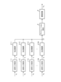
- FIG. 2 is a configuration diagram showing an adder circuit according to Embodiment 1;
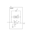
- FIG. 4 is a configuration diagram showing an amplifier circuit 4 of the adder circuit according to Embodiment 1;
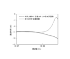
- FIG. 5 is an explanatory diagram showing an example of frequency characteristics of pass gain in the adder circuit according to Embodiment 1;
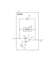
- FIG. 8 is a configuration diagram showing an amplifier circuit 4 of an adder circuit according to a second embodiment;
- FIG. 1 is a configuration diagram showing an adder circuit according to Embodiment 1.
- FIG. 2 is a configuration diagram showing the amplifier circuit 4 of the adder circuit according to the first embodiment.
- the adder circuit shown in FIG. I have.
- the amplifier circuit 4 has an operational amplifier 11 , a feedback resistor 12 and a capacitor 13 .
- a signal to be added is applied to one end of the addition input resistor 1-n.
- the voltage of the signal to be summed is Vn .
- the other end of the addition input resistor 1-n is connected to one end of the transmission line 2-n.
- the addition input resistor 1-n drops the voltage Vn of the signal to be added, and outputs the signal after the voltage drop to the transmission line 2-n.
- the adder input resistors 1-n are realized by chip resistors or metal film resistors.
- the addition input resistors 1-n only need to drop the voltage Vn of the signals to be added, and may be implemented by active elements such as transistors. Further, the addition input resistor 1-n may be a resistor with a fixed resistance value or a resistor with a variable resistance value.
- One end of the transmission line 2-n is connected to the other end of the addition input resistor 1-n.
- the other end of the transmission line 2-n is connected to one end of the isolation resistor 3.
- FIG. The transmission line 2-n transmits to the isolation resistor 3 the signal after the voltage drop by the addition input resistor 1-n.
- the isolation resistors 3 are implemented by chip resistors or metal film resistors, for example. One end of the isolation resistor 3 is connected to all the other ends of the transmission lines 2-1 to 2-N. The other end of the isolation resistor 3 is connected to the input terminal of the amplifier circuit 4 .
- the isolation resistor 3 drops the voltage of the combined signal of the N signals that have passed through the transmission lines 2-1 to 2-N.
- the isolation resistor 3 outputs the combined signal after the voltage drop to the amplifier circuit 4 .
- the isolation resistors 3 are realized by chip resistors or metal film resistors.
- the isolation resistor 3 only needs to drop the voltage of the combined signal, and may be realized by an active element such as a transistor, for example. Further, the isolation resistor 3 may be a resistor with a fixed resistance value, or may be a resistor with a variable resistance value.
- the amplifier circuit 4 amplifies the power of the combined signal after the voltage drop by the isolation resistor 3 .
- the operational amplifier 11 is implemented by, for example, a bipolar transistor or a FET (Field Effect Transistor).
- the operational amplifier 11 has a first input terminal (hereinafter referred to as "inverting input terminal") 11a, a second input terminal (hereinafter referred to as “non-inverting input terminal”) 11b, and an output terminal 11c for outputting a signal after power amplification. and
- An output terminal 11c of the operational amplifier 11 is connected to one end of the feedback resistor 12 and one end of the capacitor 13, respectively.
- An inverting input terminal 11a of the operational amplifier 11 is connected to the other end of the isolation resistor 3, the other end of the feedback resistor 12, and the other end of the capacitor 13, respectively.
- a non-inverting input terminal 11b of the operational amplifier 11 is connected to the ground. Therefore, 0V is applied to the non-inverting input terminal 11b as a constant voltage.
- the operational amplifier 11 amplifies the voltage difference between the voltage applied to the inverting input terminal 11a and the voltage applied to the non-inverting input terminal 11b.
- a signal having a voltage VO proportional to the voltage difference is output from the output terminal 11c of the operational amplifier 11 to the outside.
- Feedback resistor 12 is realized by, for example, a chip resistor or a metal film resistor.
- One end of the feedback resistor 12 is connected to the output terminal 11c of the operational amplifier 11 and one end of the capacitor 13, respectively.
- the other end of the feedback resistor 12 is connected to the inverting input terminal 11a of the operational amplifier 11, the other end of the capacitor 13, and the other end of the isolation resistor 3, respectively.
- the feedback resistor 12 drops the voltage of the signal output from the output terminal 11 c of the operational amplifier 11 and outputs the signal after the voltage drop to the inverting input terminal 11 a of the operational amplifier 11 .
- the feedback resistor 12 is implemented by a chip resistor or a metal film resistor.
- the feedback resistor 12 only needs to be able to drop the voltage of the signal output from the output terminal 11c of the operational amplifier 11, and may be implemented by an active element such as a transistor, for example. Further, the feedback resistor 12 may be a resistor with a fixed resistance value, or may be a resistor with a variable resistance value.
- Capacitor 13 is realized, for example, by a ceramic capacitor or an electrolytic capacitor. One end of the capacitor 13 is connected to the output terminal 11c of the operational amplifier 11 and one end of the feedback resistor 12, respectively. The other end of the capacitor 13 is connected to the inverting input terminal 11a of the operational amplifier 11, the other end of the feedback resistor 12, and the other end of the isolation resistor 3, respectively.
- the capacitor 13 has a capacitance for storing electric charge according to the potential difference between the voltage applied to the output terminal 11c of the operational amplifier 11 and the voltage applied to the inverting input terminal 11a.
- the capacitor 13 is provided to maintain stability of the amplifier circuit 4 to which negative feedback is applied. Therefore, the capacitance of the capacitor 13 is determined according to desired frequency characteristics or stability.
- the capacitor 13 is implemented by a ceramic capacitor or an electrolytic capacitor. However, this is only an example, and capacitor 13 may be realized by an active element such as a transistor. Further, the capacitor 13 may be a capacitor with a fixed capacitance value, or may be a capacitor with a variable capacitance value.
- each of the addition input resistors 1-1 to 1-4 is RCH
- the resistance value of the isolation resistor 3 is RIS
- the resistance value of the feedback resistor 12 is RRE .
- the four signals to be added have the same voltage Vn .
- each of the line connecting the addition input resistor 1-n and the transmission line 2-n, the line connecting the transmission line 2-n and the isolation resistor 3, and the line connecting the isolation resistor 3 and the amplifier circuit 4 has , should be free of parasitic components.
- N signals that have passed through the transmission lines 2-1 to 2-N are combined with each other.
- the isolation resistor 3 drops the voltage V n ′ of the combined signal and outputs the combined signal after the voltage drop to the inverting input terminal 11 a of the operational amplifier 11 in the amplifier circuit 4 .
- the voltage of the combined signal after the voltage drop by the isolation resistor 3 is V n ′′, and the current of the combined signal after the voltage drop is ⁇ I.
- the effect of the parasitic capacitance of the transmission line 2-n between the addition input resistor 1-n and the operational amplifier 11 by the amount that can increase the impedance when looking at one end of the addition input resistor 1-n from the inverting input terminal 11a of the operational amplifier 11 can be made smaller.
- the feedback resistor 12 drops the voltage VO of the signal output from the output terminal 11 c of the operational amplifier 11 and outputs the signal after the voltage drop to the inverting input terminal 11 a of the operational amplifier 11 .
- the voltage VO of the signal is expressed by the following equation (4).
- the adding circuit shown in FIG. 1 and the adding circuit disclosed in Patent Document 1 differ in how to determine resistance values.
- FIG. 3 is an explanatory diagram showing an example of frequency characteristics of pass gain in the adder circuit according to the first embodiment.
- the horizontal axis indicates frequency [Hz]
- the vertical axis indicates transmission gain [dB].
- the solid line indicates the frequency characteristics of the pass gain in the adder circuit shown in FIG. 1
- the dashed line indicates the frequency characteristics of the pass gain in the adder circuit disclosed in Patent Document 1.
- N 4.
- the adder circuit disclosed in Patent Document 1 not all of the N adder input resistors can be placed near the operational amplifier due to space constraints. As the number of signals to be added increases, the number of summing input resistors also increases.
- the isolation resistor 3 is arranged near the operational amplifier 11, whether all of the N addition input resistors 1-1 to 1-N are arranged near the operational amplifier 11 or not. Regardless of the above, as shown in FIG. 3, it is possible to suppress the deterioration of the flatness of the pass gain frequency characteristic in the adder circuit.
- the number of isolation resistors 3 provided in the addition circuit shown in FIG. By arranging the isolation resistor 3 near the operational amplifier 11, if the length of the line connecting the other end of the isolation resistor 3 and the inverting input terminal 11a of the operational amplifier 11 is shortened, the separation of the isolation resistor 3 and the operational amplifier 11 is reduced.
- the parasitic capacitance generated between it and the inverting input terminal 11a becomes so small that it can be ignored.
- the length of the line connecting the other end of the isolation resistor 3 and the inverting input terminal 11a of the operational amplifier 11 is shorter than the length of the transmission line 2-n.
- the effect of the parasitic capacitance of the transmission line 2-n between the addition input resistor 1-n and the operational amplifier 11 is caused by the increase in the impedance of one end of the addition input resistor 1-n from the inverting input terminal 11a of the operational amplifier 11. becomes smaller. Stability of the adder circuit because the parasitic capacitance generated between the other end of the isolation resistor 3 and the inverting input terminal 11a of the operational amplifier 11 is negligibly small, and the effect of the parasitic capacitance of the transmission line 2-n is small. deterioration can be suppressed. In addition, it is possible to suppress the deterioration of the flatness of the frequency characteristic of the pass gain in the adder circuit.
- a plurality of transmission lines 2-1 to 2-N having one end connected to the other end, and an isolation resistor 3 having one end connected to all the other ends of the plurality of transmission lines 2-1 to 2-N.
- an amplifier circuit 4 for amplifying the power of the signal output from the other end of the isolation resistor 3 . Therefore, the adder circuit can prevent deterioration of the flatness of the frequency characteristic of the pass-through gain regardless of whether or not all of the plurality of adder input resistors 1-1 to 1-N can be arranged near the amplifier circuit 4. can be done.
- the resistance values of the addition input resistors 1-1 to 1-N are the same RCH . However, this is only an example, and the resistance values of the adding input resistors 1-1 to 1-N may be different from each other.
- the amplifier circuit 4 includes a capacitor 13.
- the capacitor 13 is provided to maintain the stability of the amplifier circuit 4 to which negative feedback is applied. Even if the amplifier circuit 4 does not include the capacitor 13, the amplifier circuit 4 does not have to include the capacitor 13 as long as the stability of the amplifier circuit 4 can be maintained.
- Embodiment 2 In the addition circuit shown in FIG. 1, the non-inverting input terminal 11b of the operational amplifier 11 is connected to the ground. In the second embodiment, an adder circuit in which the non-inverting input terminal 11b of the operational amplifier 11 is connected to the voltage source 14 will be described.
- FIG. 4 is a configuration diagram showing the amplifier circuit 4 of the adder circuit according to the second embodiment.
- Voltage source 14 outputs a constant voltage to non-inverting input terminal 11 b of operational amplifier 11 . Even when the non-inverting input terminal 11b of the operational amplifier 11 is connected to the voltage source 14, the operational amplifier 11 is applied to the inverting input terminal 11a in the same manner as when the non-inverting input terminal 11b is grounded.
- the present disclosure is suitable for addition circuits.
- first resistor 1-1 to 1-N added input resistor (first resistor), 2-1 to 2-N transmission line, 3 isolation resistor (second resistor), 4 amplifier circuit, 11 operational amplifier, 11a inverting input terminal (first input terminal), 11b non-inverting input terminal (second input terminal), 11c output terminal, 12 feedback resistor, 13 capacitor, 14 voltage source.
Landscapes
- Engineering & Computer Science (AREA)
- Power Engineering (AREA)
- Amplifiers (AREA)
Abstract
加算対象の信号が一端に与えられる複数の加算入力抵抗(1-1)~(1-N)と、それぞれの加算入力抵抗(1-n)(n=1,・・・,N)の他端と一端が接続されている複数の伝送線路(2-1)~(2-N)と、複数の伝送線路(2-1)~(2-N)の他端の全てと一端が接続されているアイソレーション抵抗(3)と、アイソレーション抵抗(3)の他端から出力された信号の電力を増幅する増幅回路(4)とを備えるように、加算回路を構成した。
Description
本開示は、加算回路に関するものである。
N個の加算対象の信号を加算する加算回路がある(特許文献1を参照)。Nは、2以上の整数である。
当該加算回路は、N個の加算入力抵抗と、オペアンプとを備えている。それぞれの加算入力抵抗の一端には、加算対象の信号が与えられる。それぞれの加算入力抵抗の他端は、オペアンプの反転入力端子と接続されている。オペアンプの非反転入力端子は、グランドと接続されている。
当該加算回路は、N個の加算入力抵抗と、オペアンプとを備えている。それぞれの加算入力抵抗の一端には、加算対象の信号が与えられる。それぞれの加算入力抵抗の他端は、オペアンプの反転入力端子と接続されている。オペアンプの非反転入力端子は、グランドと接続されている。
加算入力抵抗とオペアンプの反転入力端子とを結ぶ線路の寄生容量は、当該線路の長さが長くなるほど大きくなる。
特許文献1に開示されている加算回路では、N個の加算入力抵抗の全てがオペアンプの近くに配置できるとは限らない。加算対象の信号の数が多いほど、加算入力抵抗の数も多くなり、その結果、加算入力抵抗をオペアンプの近くに配置しにくくなるために、寄生容量の大きな加算入力抵抗の数が増える。加算回路が、寄生容量の大きな加算入力抵抗を有することで、加算回路における通過利得の周波数特性の平坦性が劣化してしまうことがあるという課題があった。
特許文献1に開示されている加算回路では、N個の加算入力抵抗の全てがオペアンプの近くに配置できるとは限らない。加算対象の信号の数が多いほど、加算入力抵抗の数も多くなり、その結果、加算入力抵抗をオペアンプの近くに配置しにくくなるために、寄生容量の大きな加算入力抵抗の数が増える。加算回路が、寄生容量の大きな加算入力抵抗を有することで、加算回路における通過利得の周波数特性の平坦性が劣化してしまうことがあるという課題があった。
本開示は、上記のような課題を解決するためになされたもので、複数の加算入力抵抗である第1の抵抗の全てを増幅回路の近くに配置できるか否かにかかわらず、通過利得の周波数特性の平坦性の劣化を防止することができる加算回路を得ることを目的とする。
本開示に係る加算回路は、加算対象の信号が一端に与えられる複数の第1の抵抗と、それぞれの第1の抵抗の他端と一端が接続されている複数の伝送線路と、複数の伝送線路の他端の全てと一端が接続されている第2の抵抗と、第2の抵抗の他端から出力された信号の電力を増幅する増幅回路とを備えたものである。
本開示によれば、複数の加算入力抵抗である第1の抵抗の全てを増幅回路の近くに配置できるか否かにかかわらず、通過利得の周波数特性の平坦性の劣化を防止することができる。
以下、本開示をより詳細に説明するために、本開示を実施するための形態について、添付の図面に従って説明する。
実施の形態1.
図1は、実施の形態1に係る加算回路を示す構成図である。
図2は、実施の形態1に係る加算回路の増幅回路4を示す構成図である。
図1に示す加算回路は、加算入力抵抗(第1の抵抗)1-1~1-N、伝送線路2-1~2-N、アイソレーション抵抗(第2の抵抗)3及び増幅回路4を備えている。
増幅回路4は、オペアンプ11、帰還抵抗12及びコンデンサ13を備えている。
図1は、実施の形態1に係る加算回路を示す構成図である。
図2は、実施の形態1に係る加算回路の増幅回路4を示す構成図である。
図1に示す加算回路は、加算入力抵抗(第1の抵抗)1-1~1-N、伝送線路2-1~2-N、アイソレーション抵抗(第2の抵抗)3及び増幅回路4を備えている。
増幅回路4は、オペアンプ11、帰還抵抗12及びコンデンサ13を備えている。
加算入力抵抗1-n(n=1,・・・,N)は、例えば、チップ抵抗、又は、金属皮膜抵抗によって実現される。Nは、2以上の整数である。
加算入力抵抗1-nの一端には、加算対象の信号が与えられる。加算対象の信号の電圧は、Vnである。
加算入力抵抗1-nの他端は、伝送線路2-nの一端と接続されている。
加算入力抵抗1-nは、加算対象の信号の電圧Vnを降下させ、電圧降下後の信号を伝送線路2-nに出力する。
図1に示す加算回路では、加算入力抵抗1-nが、チップ抵抗、又は、金属皮膜抵抗によって実現されている。加算入力抵抗1-nは、加算対象の信号の電圧Vnを降下させることができればよく、例えば、トランジスタのような能動素子によって実現されていてもよい。
また、加算入力抵抗1-nは、抵抗値が固定の抵抗であってもよいし、抵抗値が可変の抵抗であってもよい。
加算入力抵抗1-nの一端には、加算対象の信号が与えられる。加算対象の信号の電圧は、Vnである。
加算入力抵抗1-nの他端は、伝送線路2-nの一端と接続されている。
加算入力抵抗1-nは、加算対象の信号の電圧Vnを降下させ、電圧降下後の信号を伝送線路2-nに出力する。
図1に示す加算回路では、加算入力抵抗1-nが、チップ抵抗、又は、金属皮膜抵抗によって実現されている。加算入力抵抗1-nは、加算対象の信号の電圧Vnを降下させることができればよく、例えば、トランジスタのような能動素子によって実現されていてもよい。
また、加算入力抵抗1-nは、抵抗値が固定の抵抗であってもよいし、抵抗値が可変の抵抗であってもよい。
伝送線路2-n(n=1,・・・,N)は、例えば、同軸ケーブル、プリント基板上のマイクロストリップ線路、コプレーナ線路、又は、導波管によって実現される。
伝送線路2-nの一端は、加算入力抵抗1-nの他端と接続されている。
伝送線路2-nの他端は、アイソレーション抵抗3の一端と接続されている。
伝送線路2-nは、加算入力抵抗1-nによる電圧降下後の信号をアイソレーション抵抗3まで伝送させる。
伝送線路2-nの一端は、加算入力抵抗1-nの他端と接続されている。
伝送線路2-nの他端は、アイソレーション抵抗3の一端と接続されている。
伝送線路2-nは、加算入力抵抗1-nによる電圧降下後の信号をアイソレーション抵抗3まで伝送させる。
アイソレーション抵抗3は、例えば、チップ抵抗、又は、金属皮膜抵抗によって実現される。
アイソレーション抵抗3の一端は、伝送線路2-1~2-Nの他端の全てと接続されている。
アイソレーション抵抗3の他端は、増幅回路4の入力端子と接続されている。
アイソレーション抵抗3は、伝送線路2-1~2-Nを通過してきたN個の信号の合成信号の電圧を降下させる。
アイソレーション抵抗3は、電圧降下後の合成信号を増幅回路4に出力する。
アイソレーション抵抗3の抵抗値は、加算入力抵抗1-n(n=1,・・・,N)の抵抗値よりも大きい。
図1に示す加算回路では、アイソレーション抵抗3が、チップ抵抗、又は、金属皮膜抵抗によって実現されている。アイソレーション抵抗3は、合成信号の電圧を降下させることができればよく、例えば、トランジスタのような能動素子によって実現されていてもよい。
また、アイソレーション抵抗3は、抵抗値が固定の抵抗であってもよいし、抵抗値が可変の抵抗であってもよい。
アイソレーション抵抗3の一端は、伝送線路2-1~2-Nの他端の全てと接続されている。
アイソレーション抵抗3の他端は、増幅回路4の入力端子と接続されている。
アイソレーション抵抗3は、伝送線路2-1~2-Nを通過してきたN個の信号の合成信号の電圧を降下させる。
アイソレーション抵抗3は、電圧降下後の合成信号を増幅回路4に出力する。
アイソレーション抵抗3の抵抗値は、加算入力抵抗1-n(n=1,・・・,N)の抵抗値よりも大きい。
図1に示す加算回路では、アイソレーション抵抗3が、チップ抵抗、又は、金属皮膜抵抗によって実現されている。アイソレーション抵抗3は、合成信号の電圧を降下させることができればよく、例えば、トランジスタのような能動素子によって実現されていてもよい。
また、アイソレーション抵抗3は、抵抗値が固定の抵抗であってもよいし、抵抗値が可変の抵抗であってもよい。
増幅回路4は、アイソレーション抵抗3による電圧降下後の合成信号の電力を増幅する。
オペアンプ11は、例えば、バイポーラトランジスタ、又は、FET(Field Effect Transistor)によって実現される。
オペアンプ11は、第1の入力端子(以下「反転入力端子」という)11aと、第2の入力端子(以下「非反転入力端子」という)11bと、電力増幅後の信号を出力する出力端子11cとを有している。
オペアンプ11の出力端子11cは、帰還抵抗12の一端及びコンデンサ13の一端のそれぞれと接続されている。
オペアンプ11の反転入力端子11aは、アイソレーション抵抗3の他端、帰還抵抗12の他端及びコンデンサ13の他端のそれぞれと接続されている。
オペアンプ11の非反転入力端子11bは、グランドと接続されている。したがって、非反転入力端子11bには、定電圧として、0Vが印加されている。
オペアンプ11は、反転入力端子11aに印加されている電圧と非反転入力端子11bに印加されている電圧との電圧差を増幅する。
オペアンプ11の出力端子11cから、当該電圧差に比例する電圧VOを有する信号が外部に出力される。
アイソレーション抵抗3とオペアンプ11の反転入力端子11aとを結ぶ線路の長さは、伝送線路2-n(n=1,・・・,N)の長さよりも短い。
オペアンプ11は、例えば、バイポーラトランジスタ、又は、FET(Field Effect Transistor)によって実現される。
オペアンプ11は、第1の入力端子(以下「反転入力端子」という)11aと、第2の入力端子(以下「非反転入力端子」という)11bと、電力増幅後の信号を出力する出力端子11cとを有している。
オペアンプ11の出力端子11cは、帰還抵抗12の一端及びコンデンサ13の一端のそれぞれと接続されている。
オペアンプ11の反転入力端子11aは、アイソレーション抵抗3の他端、帰還抵抗12の他端及びコンデンサ13の他端のそれぞれと接続されている。
オペアンプ11の非反転入力端子11bは、グランドと接続されている。したがって、非反転入力端子11bには、定電圧として、0Vが印加されている。
オペアンプ11は、反転入力端子11aに印加されている電圧と非反転入力端子11bに印加されている電圧との電圧差を増幅する。
オペアンプ11の出力端子11cから、当該電圧差に比例する電圧VOを有する信号が外部に出力される。
アイソレーション抵抗3とオペアンプ11の反転入力端子11aとを結ぶ線路の長さは、伝送線路2-n(n=1,・・・,N)の長さよりも短い。
帰還抵抗12は、例えば、チップ抵抗、又は、金属皮膜抵抗によって実現される。
帰還抵抗12の一端は、オペアンプ11の出力端子11c及びコンデンサ13の一端のそれぞれと接続されている。
帰還抵抗12の他端は、オペアンプ11の反転入力端子11a、コンデンサ13の他端及びアイソレーション抵抗3の他端のそれぞれと接続されている。
帰還抵抗12は、オペアンプ11の出力端子11cから出力された信号の電圧を降下させ、電圧降下後の信号をオペアンプ11の反転入力端子11aに出力する。
図2に示す増幅回路4では、帰還抵抗12が、チップ抵抗、又は、金属皮膜抵抗によって実現されている。帰還抵抗12は、オペアンプ11の出力端子11cから出力された信号の電圧を降下させることができればよく、例えば、トランジスタのような能動素子によって実現されていてもよい。
また、帰還抵抗12は、抵抗値が固定の抵抗であってもよいし、抵抗値が可変の抵抗であってもよい。
帰還抵抗12の一端は、オペアンプ11の出力端子11c及びコンデンサ13の一端のそれぞれと接続されている。
帰還抵抗12の他端は、オペアンプ11の反転入力端子11a、コンデンサ13の他端及びアイソレーション抵抗3の他端のそれぞれと接続されている。
帰還抵抗12は、オペアンプ11の出力端子11cから出力された信号の電圧を降下させ、電圧降下後の信号をオペアンプ11の反転入力端子11aに出力する。
図2に示す増幅回路4では、帰還抵抗12が、チップ抵抗、又は、金属皮膜抵抗によって実現されている。帰還抵抗12は、オペアンプ11の出力端子11cから出力された信号の電圧を降下させることができればよく、例えば、トランジスタのような能動素子によって実現されていてもよい。
また、帰還抵抗12は、抵抗値が固定の抵抗であってもよいし、抵抗値が可変の抵抗であってもよい。
コンデンサ13は、例えば、セラミックコンデンサ、又は、電界コンデンサによって実現される。
コンデンサ13の一端は、オペアンプ11の出力端子11c及び帰還抵抗12の一端のそれぞれと接続されている。
コンデンサ13の他端は、オペアンプ11の反転入力端子11a、帰還抵抗12の他端及びアイソレーション抵抗3の他端のそれぞれと接続されている。
コンデンサ13は、オペアンプ11の出力端子11cに印加されている電圧と反転入力端子11aに印加されている電圧との電位差に応じた電荷を蓄える静電容量を有している。
コンデンサ13は、負帰還をかけている増幅回路4の安定性を保つために設けられている。このため、コンデンサ13が有する静電容量は、所望の周波数特性、又は、安定性に応じて決定される。
図2に示す増幅回路4では、コンデンサ13が、セラミックコンデンサ、又は、電界コンデンサによって実現されている。しかし、これは一例に過ぎず、コンデンサ13は、トランジスタのような能動素子によって実現されていてもよい。
また、コンデンサ13は、容量値が固定のコンデンサであってもよいし、容量値が可変のコンデンサであってもよい。
コンデンサ13の一端は、オペアンプ11の出力端子11c及び帰還抵抗12の一端のそれぞれと接続されている。
コンデンサ13の他端は、オペアンプ11の反転入力端子11a、帰還抵抗12の他端及びアイソレーション抵抗3の他端のそれぞれと接続されている。
コンデンサ13は、オペアンプ11の出力端子11cに印加されている電圧と反転入力端子11aに印加されている電圧との電位差に応じた電荷を蓄える静電容量を有している。
コンデンサ13は、負帰還をかけている増幅回路4の安定性を保つために設けられている。このため、コンデンサ13が有する静電容量は、所望の周波数特性、又は、安定性に応じて決定される。
図2に示す増幅回路4では、コンデンサ13が、セラミックコンデンサ、又は、電界コンデンサによって実現されている。しかし、これは一例に過ぎず、コンデンサ13は、トランジスタのような能動素子によって実現されていてもよい。
また、コンデンサ13は、容量値が固定のコンデンサであってもよいし、容量値が可変のコンデンサであってもよい。
次に、図1に示す加算回路の動作について説明する。
ここでは、説明の便宜上、N=4の例を説明する。
また、加算入力抵抗1-1~1-4におけるそれぞれの抵抗値がRCHであり、アイソレーション抵抗3の抵抗値がRISであり、帰還抵抗12の抵抗値がRREであるものとする。
また、4つの加算対象の信号の電圧Vnが同じであるものとする。V1=V2=V3=V4である。
さらに、加算入力抵抗1-nと伝送線路2-nとを結ぶ線路、伝送線路2-nとアイソレーション抵抗3とを結ぶ線路及びアイソレーション抵抗3と増幅回路4とを結ぶ線路のそれぞれには、寄生成分が無いものとする。
ここでは、説明の便宜上、N=4の例を説明する。
また、加算入力抵抗1-1~1-4におけるそれぞれの抵抗値がRCHであり、アイソレーション抵抗3の抵抗値がRISであり、帰還抵抗12の抵抗値がRREであるものとする。
また、4つの加算対象の信号の電圧Vnが同じであるものとする。V1=V2=V3=V4である。
さらに、加算入力抵抗1-nと伝送線路2-nとを結ぶ線路、伝送線路2-nとアイソレーション抵抗3とを結ぶ線路及びアイソレーション抵抗3と増幅回路4とを結ぶ線路のそれぞれには、寄生成分が無いものとする。
加算入力抵抗1-n(n=1,・・・,4)は、加算対象の信号が与えられると、加算対象の信号の電圧Vnを降下させ、電圧降下後の信号を伝送線路2-nに出力する。
電圧降下後の信号の電圧は、Vn’であり、Vn>Vn’である。V1=V2=V3=V4であって、加算入力抵抗1-1~1-Nにおけるそれぞれの抵抗値は、同じRCHであるため、V1’=V2’=V3’=V4’である。
加算入力抵抗1-nから伝送線路2-nには、電流Inが流れる。V1=V2=V3=V4であって、加算入力抵抗1-1~1-Nにおけるそれぞれの抵抗値は、同じRCHであるため、I1=I2=I3=I4=Iである。
電圧降下後の信号の電圧は、Vn’であり、Vn>Vn’である。V1=V2=V3=V4であって、加算入力抵抗1-1~1-Nにおけるそれぞれの抵抗値は、同じRCHであるため、V1’=V2’=V3’=V4’である。
加算入力抵抗1-nから伝送線路2-nには、電流Inが流れる。V1=V2=V3=V4であって、加算入力抵抗1-1~1-Nにおけるそれぞれの抵抗値は、同じRCHであるため、I1=I2=I3=I4=Iである。
伝送線路2-n(n=1,・・・,4)は、加算入力抵抗1-nから、電圧がVn’で、電流がInの信号を受けると、当該信号をアイソレーション抵抗3まで伝送させる。
伝送線路2-1~2-Nを通過してきたN個の信号は、互いに合成される。N個の信号の合成信号の電圧は、Vn’であり、合成信号の電流ΣIは、以下の式(1)のように表される。
ΣI=I1+I2+I3+I4 (1)
ΣI=I1+I2+I3+I4 (1)
I1=I2=I3=I4=Iであるため、合成信号の電流ΣIは、以下の式(2)のように表される。
ΣI=4I (2)
ΣI=4I (2)
アイソレーション抵抗3は、合成信号の電圧Vn’を降下させ、電圧降下後の合成信号を増幅回路4におけるオペアンプ11の反転入力端子11aに出力する。
アイソレーション抵抗3による電圧降下後の合成信号の電圧は、Vn”であり、電圧降下後の合成信号の電流は、ΣIである。
アイソレーション抵抗3の抵抗値RISは、加算入力抵抗1-n(n=1,・・・,4)の抵抗値RCHよりも大きい。このため、オペアンプ11の反転入力端子11aから加算入力抵抗1-nの一端を見たインピーダンスを大きくすることができる。オペアンプ11の反転入力端子11aから加算入力抵抗1-nの一端を見たインピーダンスを大きくできる分だけ、加算入力抵抗1-nとオペアンプ11との間にある伝送線路2-nの寄生容量の影響を小さくすることができる。
アイソレーション抵抗3による電圧降下後の合成信号の電圧は、Vn”であり、電圧降下後の合成信号の電流は、ΣIである。
アイソレーション抵抗3の抵抗値RISは、加算入力抵抗1-n(n=1,・・・,4)の抵抗値RCHよりも大きい。このため、オペアンプ11の反転入力端子11aから加算入力抵抗1-nの一端を見たインピーダンスを大きくすることができる。オペアンプ11の反転入力端子11aから加算入力抵抗1-nの一端を見たインピーダンスを大きくできる分だけ、加算入力抵抗1-nとオペアンプ11との間にある伝送線路2-nの寄生容量の影響を小さくすることができる。
オペアンプ11の非反転入力端子11bは、グランドと接続されているため、負帰還をかけたイマジナリーショートが成立している。このため、オペアンプ11の反転入力端子11aの電位は、非反転入力端子11bと同じ電位になる。即ち、オペアンプ11の反転入力端子11aの電位は、0[V]になる。
したがって、加算対象の信号の電圧Vn(n=1,・・・,4)は、以下の式(3)のように表される。
Vn=RCH・In+RIS・ΣI (3)
したがって、加算対象の信号の電圧Vn(n=1,・・・,4)は、以下の式(3)のように表される。
Vn=RCH・In+RIS・ΣI (3)
帰還抵抗12は、オペアンプ11の出力端子11cから出力された信号の電圧VOを降下させ、電圧降下後の信号をオペアンプ11の反転入力端子11aに出力する。
帰還抵抗12を流れる電流がIREであるとすれば、信号の電圧VOは、以下の式(4)のように表される。
帰還抵抗12を流れる電流がIREであるとすれば、信号の電圧VOは、以下の式(4)のように表される。
VO=RRE・IRE (4)
IRE=ΣI (5)
また、式(2)~(5)より、信号の電圧VOは、以下の式(6)のように表される。
IRE=ΣI (5)
また、式(2)~(5)より、信号の電圧VOは、以下の式(6)のように表される。

例えば、4つの加算対象の信号が等振幅で加算される場合において、オペアンプ11の利得が、VO=4Vnとなるような利得を有していれば、以下の式(7)が成立する。
RCH+4RIS=RRE (7)
ここでは、N=4の例を示しているが、Nを一般化すれば、以下の式(8)が成立する。
RCH+N・RIS=RRE(8)
RCH+4RIS=RRE (7)
ここでは、N=4の例を示しているが、Nを一般化すれば、以下の式(8)が成立する。
RCH+N・RIS=RRE(8)
特許文献1に開示されている加算回路では、N個の抵抗(以下「加算入力抵抗」という)の抵抗値がRCH、オペアンプの反転入力端子とオペアンプの出力端子との間に接続されている帰還抵抗の抵抗値がRREであるとすれば、以下の式(9)が成立する。
N・RCH=RRE (9)
N・RCH=RRE (9)
式(8)及び式(9)が示すように、図1に示す加算回路と、特許文献1に開示されている加算回路とでは、抵抗値の決め方が異なる。
図3は、実施の形態1に係る加算回路における通過利得の周波数特性の一例を示す説明図である。
図3において、横軸は周波数[Hz]を示し、縦軸は通過利得[dB]を示している。
また、実線は、図1に示す加算回路における通過利得の周波数特性を示し、破線は、特許文献1に開示されている加算回路における通過利得の周波数特性を示している。図3の例では、N=4である。
特許文献1に開示されている加算回路では、スペースの都合上、N個の加算入力抵抗の全てがオペアンプの近くに配置できるとは限らない。加算対象の信号の数が多いほど、加算入力抵抗の数も多くなり、その結果、加算入力抵抗をオペアンプの近くに配置しにくくなるために、寄生容量の大きな加算入力抵抗の数が増える。当該加算回路が、寄生容量の大きな加算入力抵抗を有することで、当該加算回路の安定性が劣化してしまうことがある。また、図3に示すように、当該加算回路における通過利得の周波数特性の平坦性が劣化してしまうことがある。
図3において、横軸は周波数[Hz]を示し、縦軸は通過利得[dB]を示している。
また、実線は、図1に示す加算回路における通過利得の周波数特性を示し、破線は、特許文献1に開示されている加算回路における通過利得の周波数特性を示している。図3の例では、N=4である。
特許文献1に開示されている加算回路では、スペースの都合上、N個の加算入力抵抗の全てがオペアンプの近くに配置できるとは限らない。加算対象の信号の数が多いほど、加算入力抵抗の数も多くなり、その結果、加算入力抵抗をオペアンプの近くに配置しにくくなるために、寄生容量の大きな加算入力抵抗の数が増える。当該加算回路が、寄生容量の大きな加算入力抵抗を有することで、当該加算回路の安定性が劣化してしまうことがある。また、図3に示すように、当該加算回路における通過利得の周波数特性の平坦性が劣化してしまうことがある。
図1に示す加算回路では、アイソレーション抵抗3がオペアンプ11の近くに配置されていれば、N個の加算入力抵抗1-1~1-Nの全てがオペアンプ11の近くに配置されているか否かにかかわらず、図3に示すように、加算回路における通過利得の周波数特性の平坦性の劣化を抑えることができる。
図1に示す加算回路が備えるアイソレーション抵抗3の数は、1つであり、1つのアイソレーション抵抗3だけであれば、アイソレーション抵抗3をオペアンプ11の近くに配置できる可能性が高い。アイソレーション抵抗3をオペアンプ11の近くに配置することで、アイソレーション抵抗3の他端とオペアンプ11の反転入力端子11aとを結ぶ線路の長さが短くなれば、アイソレーション抵抗3とオペアンプ11の反転入力端子11aとの間に生じる寄生容量が、無視できるほどに小さくなる。図1に示す加算回路では、アイソレーション抵抗3の他端とオペアンプ11の反転入力端子11aとを結ぶ線路の長さが、伝送線路2-nの長さよりも短い。
図1に示す加算回路が備えるアイソレーション抵抗3の数は、1つであり、1つのアイソレーション抵抗3だけであれば、アイソレーション抵抗3をオペアンプ11の近くに配置できる可能性が高い。アイソレーション抵抗3をオペアンプ11の近くに配置することで、アイソレーション抵抗3の他端とオペアンプ11の反転入力端子11aとを結ぶ線路の長さが短くなれば、アイソレーション抵抗3とオペアンプ11の反転入力端子11aとの間に生じる寄生容量が、無視できるほどに小さくなる。図1に示す加算回路では、アイソレーション抵抗3の他端とオペアンプ11の反転入力端子11aとを結ぶ線路の長さが、伝送線路2-nの長さよりも短い。
また、図1に示す加算回路では、アイソレーション抵抗3の抵抗値RISが、加算入力抵抗1-n(n=1,・・・,4)の抵抗値RCHよりも大きい。アイソレーション抵抗3の抵抗値RISが、加算入力抵抗1-nの抵抗値RCHよりも大きければ、アイソレーション抵抗3が設けられていない加算回路よりも、オペアンプ11の反転入力端子11aから加算入力抵抗1-nの一端を見たインピーダンスが大きくなる。オペアンプ11の反転入力端子11aから加算入力抵抗1-nの一端を見たインピーダンスが大きくなることで、加算入力抵抗1-nとオペアンプ11との間にある伝送線路2-nの寄生容量の影響が小さくなる。
アイソレーション抵抗3の他端とオペアンプ11の反転入力端子11aとの間に生じる寄生容量が無視できるほどに小さく、かつ、伝送線路2-nの寄生容量の影響が小さいため、加算回路の安定性の劣化を抑えることができる。また、加算回路における通過利得の周波数特性の平坦性の劣化を抑えることができる。
アイソレーション抵抗3の他端とオペアンプ11の反転入力端子11aとの間に生じる寄生容量が無視できるほどに小さく、かつ、伝送線路2-nの寄生容量の影響が小さいため、加算回路の安定性の劣化を抑えることができる。また、加算回路における通過利得の周波数特性の平坦性の劣化を抑えることができる。
以上の実施の形態1では、加算対象の信号が一端に与えられる複数の加算入力抵抗1-1~1-Nと、それぞれの加算入力抵抗1-n(n=1,・・・,N)の他端と一端が接続されている複数の伝送線路2-1~2-Nと、複数の伝送線路2-1~2-Nの他端の全てと一端が接続されているアイソレーション抵抗3と、アイソレーション抵抗3の他端から出力された信号の電力を増幅する増幅回路4とを備えるように、加算回路を構成した。したがって、加算回路は、複数の加算入力抵抗1-1~1-Nの全てを増幅回路4の近くに配置できるか否かにかかわらず、通過利得の周波数特性の平坦性の劣化を防止することができる。
図1に示す加算回路では、加算入力抵抗1-1~1-Nにおけるそれぞれの抵抗値が同じRCHであるものを示している。しかし、これは一例に過ぎず、加算入力抵抗1-1~1-Nにおけるそれぞれの抵抗値が互いに異なっていてもよい。
図1に示す加算回路では、増幅回路4がコンデンサ13を備えている。コンデンサ13は、負帰還をかけた増幅回路4の安定性を保つために設けられている。増幅回路4がコンデンサ13を備えていなくても、増幅回路4の安定性を保つことができれば、増幅回路4がコンデンサ13を備えていなくてもよい。
実施の形態2.
図1に示す加算回路では、オペアンプ11の非反転入力端子11bがグランドと接続されている。
実施の形態2では、オペアンプ11の非反転入力端子11bが電圧源14と接続されている加算回路について説明する。
図1に示す加算回路では、オペアンプ11の非反転入力端子11bがグランドと接続されている。
実施の形態2では、オペアンプ11の非反転入力端子11bが電圧源14と接続されている加算回路について説明する。
実施の形態2に係る加算回路の構成は、実施の形態1に係る加算回路の構成と同様であり、実施の形態2に係る加算回路を示す構成図は、図1である。
図4は、実施の形態2に係る加算回路の増幅回路4を示す構成図である。図4において、図2と同一符号は同一又は相当部分を示すので説明を省略する。
電圧源14は、定電圧をオペアンプ11の非反転入力端子11bに出力する。
オペアンプ11の非反転入力端子11bが電圧源14と接続されている場合も、非反転入力端子11bがグランドと接続されている場合と同様に、オペアンプ11は、反転入力端子11aに印加されている電圧と非反転入力端子11bに印加されている電圧との電圧差を増幅する。
したがって、実施の形態2に係る加算回路は、実施の形態1に係る加算回路と同様に、複数の加算入力抵抗1-1~1-Nの全てを増幅回路4の近くに配置できるか否かにかかわらず、通過利得の周波数特性の平坦性の劣化を防止することができる。
図4は、実施の形態2に係る加算回路の増幅回路4を示す構成図である。図4において、図2と同一符号は同一又は相当部分を示すので説明を省略する。
電圧源14は、定電圧をオペアンプ11の非反転入力端子11bに出力する。
オペアンプ11の非反転入力端子11bが電圧源14と接続されている場合も、非反転入力端子11bがグランドと接続されている場合と同様に、オペアンプ11は、反転入力端子11aに印加されている電圧と非反転入力端子11bに印加されている電圧との電圧差を増幅する。
したがって、実施の形態2に係る加算回路は、実施の形態1に係る加算回路と同様に、複数の加算入力抵抗1-1~1-Nの全てを増幅回路4の近くに配置できるか否かにかかわらず、通過利得の周波数特性の平坦性の劣化を防止することができる。
なお、本開示は、各実施の形態の自由な組み合わせ、あるいは各実施の形態の任意の構成要素の変形、もしくは各実施の形態において任意の構成要素の省略が可能である。
本開示は、加算回路に適している。
1-1~1-N 加算入力抵抗(第1の抵抗)、2-1~2-N 伝送線路、3 アイソレーション抵抗(第2の抵抗)、4 増幅回路、11 オペアンプ、11a 反転入力端子(第1の入力端子)、11b 非反転入力端子(第2の入力端子)、11c 出力端子、12 帰還抵抗、13 コンデンサ、14 電圧源。
Claims (6)
- 加算対象の信号が一端に与えられる複数の第1の抵抗と、
それぞれの第1の抵抗の他端と一端が接続されている複数の伝送線路と、
前記複数の伝送線路の他端の全てと一端が接続されている第2の抵抗と、
前記第2の抵抗の他端から出力された信号の電力を増幅する増幅回路と
を備えた加算回路。 - 前記増幅回路は、
前記第2の抵抗の他端から出力された信号が与えられる第1の入力端子と、定電圧が印加される第2の入力端子と、電力増幅後の信号を出力する出力端子とを有するオペアンプと、
前記オペアンプの出力端子と一端が接続され、前記第1の入力端子と他端が接続されている帰還抵抗と
を備えていることを特徴とする請求項1記載の加算回路。 - 前記第1の入力端子が反転入力端子であり、前記第2の入力端子が非反転入力端子であることを特徴とする請求項2記載の加算回路。
- 前記増幅回路は、
前記オペアンプの出力端子と一端が接続され、前記第1の入力端子と他端が接続されているコンデンサを備えていることを特徴とする請求項2記載の加算回路。 - 前記第2の抵抗の抵抗値が、それぞれの第1の抵抗の抵抗値よりも大きいことを特徴とする請求項1記載の加算回路。
- 前記第2の抵抗と前記増幅回路とを結ぶ線路の長さが、それぞれの伝送線路の長さよりも短いことを特徴とする請求項1記載の加算回路。
Priority Applications (1)
| Application Number | Priority Date | Filing Date | Title |
|---|---|---|---|
| PCT/JP2021/044064 WO2023100285A1 (ja) | 2021-12-01 | 2021-12-01 | 加算回路 |
Applications Claiming Priority (1)
| Application Number | Priority Date | Filing Date | Title |
|---|---|---|---|
| PCT/JP2021/044064 WO2023100285A1 (ja) | 2021-12-01 | 2021-12-01 | 加算回路 |
Publications (1)
| Publication Number | Publication Date |
|---|---|
| WO2023100285A1 true WO2023100285A1 (ja) | 2023-06-08 |
Family
ID=86611779
Family Applications (1)
| Application Number | Title | Priority Date | Filing Date |
|---|---|---|---|
| PCT/JP2021/044064 Ceased WO2023100285A1 (ja) | 2021-12-01 | 2021-12-01 | 加算回路 |
Country Status (1)
| Country | Link |
|---|---|
| WO (1) | WO2023100285A1 (ja) |
Citations (3)
| Publication number | Priority date | Publication date | Assignee | Title |
|---|---|---|---|---|
| JPS63172516A (ja) * | 1987-01-09 | 1988-07-16 | Matsushita Electric Ind Co Ltd | Pwm信号出力回路 |
| JP2010056926A (ja) * | 2008-08-28 | 2010-03-11 | Yamaha Corp | D/a変換回路およびデジタル入力型d級増幅器 |
| JP2014099809A (ja) * | 2012-11-15 | 2014-05-29 | Asahi Kasei Electronics Co Ltd | バッファ回路 |
-
2021
- 2021-12-01 WO PCT/JP2021/044064 patent/WO2023100285A1/ja not_active Ceased
Patent Citations (3)
| Publication number | Priority date | Publication date | Assignee | Title |
|---|---|---|---|---|
| JPS63172516A (ja) * | 1987-01-09 | 1988-07-16 | Matsushita Electric Ind Co Ltd | Pwm信号出力回路 |
| JP2010056926A (ja) * | 2008-08-28 | 2010-03-11 | Yamaha Corp | D/a変換回路およびデジタル入力型d級増幅器 |
| JP2014099809A (ja) * | 2012-11-15 | 2014-05-29 | Asahi Kasei Electronics Co Ltd | バッファ回路 |
Similar Documents
| Publication | Publication Date | Title |
|---|---|---|
| US20100109739A1 (en) | Active guarding for reduction of resistive and capacitive signal loading with adjustable control of compensation level | |
| JP7763320B2 (ja) | 無線周波数電力増幅器システムおよびその出力信号を線形化する方法 | |
| US7592865B2 (en) | Power amplifier using power combiner | |
| EP3683963B1 (en) | A negative impedance circuit and corresponding device | |
| TWI655843B (zh) | 多路射頻功率放大裝置 | |
| US8134407B2 (en) | Enhancing dual op-amps for differential connections | |
| CN102577287B (zh) | 高速对内去偏斜电路 | |
| CN106328035A (zh) | 公共电压补偿电路、其补偿方法、显示面板及显示装置 | |
| US9559647B2 (en) | Amplifier circuit | |
| US20220123702A1 (en) | Distributed Circuit | |
| CN106505985B (zh) | 单端至差分转换电路及信号处理模块 | |
| US7642849B2 (en) | Multiple-input and multiple-output amplifier | |
| WO2023100285A1 (ja) | 加算回路 | |
| JP2010220195A (ja) | カレントコンベアベースの計器増幅器 | |
| US7123080B2 (en) | Differential amplification input circuit | |
| JP6503344B2 (ja) | 多段増幅のための方法及び回路要素 | |
| US10284152B2 (en) | Amplifier, audio signal output method, and electronic device | |
| US20180109227A1 (en) | Amplifier with adjustable gain | |
| JP5088099B2 (ja) | 映像信号増幅回路および増幅用半導体集積回路 | |
| US20210203281A1 (en) | Low noise amplifier | |
| CN114337560A (zh) | 差动放大器 | |
| JP4839572B2 (ja) | 入力回路 | |
| US8222947B2 (en) | Low distortion active balun circuit and method thereof | |
| US7057463B2 (en) | Differential amplifier with improved frequency characteristic | |
| US11929539B2 (en) | Directional coupler and semiconductor chip |
Legal Events
| Date | Code | Title | Description |
|---|---|---|---|
| 121 | Ep: the epo has been informed by wipo that ep was designated in this application |
Ref document number: 21966369 Country of ref document: EP Kind code of ref document: A1 |
|
| NENP | Non-entry into the national phase |
Ref country code: DE |
|
| 122 | Ep: pct application non-entry in european phase |
Ref document number: 21966369 Country of ref document: EP Kind code of ref document: A1 |
|
| NENP | Non-entry into the national phase |
Ref country code: JP |