WO2023100013A1 - Dispositif à semi-conducteurs et procédé de fabrication de dispositif à semi-conducteurs - Google Patents
Dispositif à semi-conducteurs et procédé de fabrication de dispositif à semi-conducteurs Download PDFInfo
- Publication number
- WO2023100013A1 WO2023100013A1 PCT/IB2022/061054 IB2022061054W WO2023100013A1 WO 2023100013 A1 WO2023100013 A1 WO 2023100013A1 IB 2022061054 W IB2022061054 W IB 2022061054W WO 2023100013 A1 WO2023100013 A1 WO 2023100013A1
- Authority
- WO
- WIPO (PCT)
- Prior art keywords
- insulator
- conductor
- oxide
- region
- oxygen
- Prior art date
Links
- 239000004065 semiconductor Substances 0.000 title claims abstract description 353
- 238000004519 manufacturing process Methods 0.000 title claims abstract description 62
- 238000000034 method Methods 0.000 title claims description 216
- 239000012212 insulator Substances 0.000 claims abstract description 1091
- 239000004020 conductor Substances 0.000 claims abstract description 642
- 229910052760 oxygen Inorganic materials 0.000 claims abstract description 301
- 239000001301 oxygen Substances 0.000 claims abstract description 299
- QVGXLLKOCUKJST-UHFFFAOYSA-N atomic oxygen Chemical compound [O] QVGXLLKOCUKJST-UHFFFAOYSA-N 0.000 claims abstract description 291
- 229910044991 metal oxide Inorganic materials 0.000 claims abstract description 116
- 150000004706 metal oxides Chemical class 0.000 claims abstract description 115
- 229910052751 metal Inorganic materials 0.000 claims abstract description 62
- 239000002184 metal Substances 0.000 claims abstract description 53
- 229910052739 hydrogen Inorganic materials 0.000 claims description 169
- 239000001257 hydrogen Substances 0.000 claims description 169
- UFHFLCQGNIYNRP-UHFFFAOYSA-N Hydrogen Chemical compound [H][H] UFHFLCQGNIYNRP-UHFFFAOYSA-N 0.000 claims description 158
- IJGRMHOSHXDMSA-UHFFFAOYSA-N Atomic nitrogen Chemical compound N#N IJGRMHOSHXDMSA-UHFFFAOYSA-N 0.000 claims description 109
- 239000000463 material Substances 0.000 claims description 92
- 229910052782 aluminium Inorganic materials 0.000 claims description 77
- XAGFODPZIPBFFR-UHFFFAOYSA-N aluminium Chemical compound [Al] XAGFODPZIPBFFR-UHFFFAOYSA-N 0.000 claims description 77
- 239000011701 zinc Substances 0.000 claims description 55
- 229910052710 silicon Inorganic materials 0.000 claims description 49
- 239000010703 silicon Substances 0.000 claims description 49
- 229910052757 nitrogen Inorganic materials 0.000 claims description 48
- 239000012298 atmosphere Substances 0.000 claims description 46
- 238000012545 processing Methods 0.000 claims description 46
- 229910052715 tantalum Inorganic materials 0.000 claims description 46
- GUVRBAGPIYLISA-UHFFFAOYSA-N tantalum atom Chemical group [Ta] GUVRBAGPIYLISA-UHFFFAOYSA-N 0.000 claims description 46
- 229910052738 indium Inorganic materials 0.000 claims description 27
- APFVFJFRJDLVQX-UHFFFAOYSA-N indium atom Chemical compound [In] APFVFJFRJDLVQX-UHFFFAOYSA-N 0.000 claims description 25
- RTAQQCXQSZGOHL-UHFFFAOYSA-N Titanium Chemical compound [Ti] RTAQQCXQSZGOHL-UHFFFAOYSA-N 0.000 claims description 23
- 229910052719 titanium Inorganic materials 0.000 claims description 23
- 239000010936 titanium Substances 0.000 claims description 23
- 229910052725 zinc Inorganic materials 0.000 claims description 12
- HCHKCACWOHOZIP-UHFFFAOYSA-N Zinc Chemical compound [Zn] HCHKCACWOHOZIP-UHFFFAOYSA-N 0.000 claims description 8
- 230000010354 integration Effects 0.000 abstract description 2
- 239000010408 film Substances 0.000 description 434
- 239000010410 layer Substances 0.000 description 281
- 108091006146 Channels Proteins 0.000 description 163
- 239000000758 substrate Substances 0.000 description 157
- 230000006870 function Effects 0.000 description 145
- 230000002829 reductive effect Effects 0.000 description 122
- 238000010438 heat treatment Methods 0.000 description 103
- 238000004544 sputter deposition Methods 0.000 description 99
- 230000015572 biosynthetic process Effects 0.000 description 97
- 239000012535 impurity Substances 0.000 description 92
- 239000007789 gas Substances 0.000 description 79
- 238000000231 atomic layer deposition Methods 0.000 description 56
- VYPSYNLAJGMNEJ-UHFFFAOYSA-N Silicium dioxide Chemical compound O=[Si]=O VYPSYNLAJGMNEJ-UHFFFAOYSA-N 0.000 description 55
- XLYOFNOQVPJJNP-UHFFFAOYSA-N water Substances O XLYOFNOQVPJJNP-UHFFFAOYSA-N 0.000 description 50
- 229910001868 water Inorganic materials 0.000 description 50
- XUIMIQQOPSSXEZ-UHFFFAOYSA-N Silicon Chemical compound [Si] XUIMIQQOPSSXEZ-UHFFFAOYSA-N 0.000 description 49
- 238000009792 diffusion process Methods 0.000 description 48
- 229910052581 Si3N4 Inorganic materials 0.000 description 47
- HQVNEWCFYHHQES-UHFFFAOYSA-N silicon nitride Chemical compound N12[Si]34N5[Si]62N3[Si]51N64 HQVNEWCFYHHQES-UHFFFAOYSA-N 0.000 description 47
- 239000013078 crystal Substances 0.000 description 45
- 229910052814 silicon oxide Inorganic materials 0.000 description 43
- TWNQGVIAIRXVLR-UHFFFAOYSA-N oxo(oxoalumanyloxy)alumane Chemical compound O=[Al]O[Al]=O TWNQGVIAIRXVLR-UHFFFAOYSA-N 0.000 description 41
- 150000004767 nitrides Chemical class 0.000 description 40
- 238000005229 chemical vapour deposition Methods 0.000 description 39
- 229920005989 resin Polymers 0.000 description 36
- 239000011347 resin Substances 0.000 description 36
- 239000000203 mixture Substances 0.000 description 34
- 229910052735 hafnium Inorganic materials 0.000 description 33
- 238000010586 diagram Methods 0.000 description 32
- 230000007423 decrease Effects 0.000 description 30
- 239000012044 organic layer Substances 0.000 description 30
- 238000012546 transfer Methods 0.000 description 30
- 230000004888 barrier function Effects 0.000 description 29
- VBJZVLUMGGDVMO-UHFFFAOYSA-N hafnium atom Chemical compound [Hf] VBJZVLUMGGDVMO-UHFFFAOYSA-N 0.000 description 29
- 239000003990 capacitor Substances 0.000 description 28
- 238000004549 pulsed laser deposition Methods 0.000 description 27
- 229910052733 gallium Inorganic materials 0.000 description 26
- -1 hafnium aluminate Chemical class 0.000 description 26
- 238000001451 molecular beam epitaxy Methods 0.000 description 26
- GYHNNYVSQQEPJS-UHFFFAOYSA-N Gallium Chemical compound [Ga] GYHNNYVSQQEPJS-UHFFFAOYSA-N 0.000 description 22
- PXHVJJICTQNCMI-UHFFFAOYSA-N Nickel Chemical group [Ni] PXHVJJICTQNCMI-UHFFFAOYSA-N 0.000 description 22
- 125000004429 atom Chemical group 0.000 description 22
- 230000007547 defect Effects 0.000 description 20
- 229910001882 dioxygen Inorganic materials 0.000 description 19
- 238000005530 etching Methods 0.000 description 19
- 239000002356 single layer Substances 0.000 description 19
- 229910052721 tungsten Inorganic materials 0.000 description 19
- 239000010937 tungsten Substances 0.000 description 19
- MYMOFIZGZYHOMD-UHFFFAOYSA-N Dioxygen Chemical compound O=O MYMOFIZGZYHOMD-UHFFFAOYSA-N 0.000 description 18
- 230000005669 field effect Effects 0.000 description 18
- 239000000126 substance Substances 0.000 description 18
- WFKWXMTUELFFGS-UHFFFAOYSA-N tungsten Chemical compound [W] WFKWXMTUELFFGS-UHFFFAOYSA-N 0.000 description 18
- 238000004140 cleaning Methods 0.000 description 17
- 238000001312 dry etching Methods 0.000 description 17
- 230000002349 favourable effect Effects 0.000 description 17
- XLOMVQKBTHCTTD-UHFFFAOYSA-N Zinc monoxide Chemical compound [Zn]=O XLOMVQKBTHCTTD-UHFFFAOYSA-N 0.000 description 16
- 238000000151 deposition Methods 0.000 description 16
- 229910000449 hafnium oxide Inorganic materials 0.000 description 16
- WIHZLLGSGQNAGK-UHFFFAOYSA-N hafnium(4+);oxygen(2-) Chemical compound [O-2].[O-2].[Hf+4] WIHZLLGSGQNAGK-UHFFFAOYSA-N 0.000 description 16
- OKTJSMMVPCPJKN-UHFFFAOYSA-N Carbon Chemical compound [C] OKTJSMMVPCPJKN-UHFFFAOYSA-N 0.000 description 15
- RYGMFSIKBFXOCR-UHFFFAOYSA-N Copper Chemical group [Cu] RYGMFSIKBFXOCR-UHFFFAOYSA-N 0.000 description 15
- NRTOMJZYCJJWKI-UHFFFAOYSA-N Titanium nitride Chemical compound [Ti]#N NRTOMJZYCJJWKI-UHFFFAOYSA-N 0.000 description 15
- 230000008021 deposition Effects 0.000 description 15
- 230000003647 oxidation Effects 0.000 description 15
- 238000007254 oxidation reaction Methods 0.000 description 15
- 229910001873 dinitrogen Inorganic materials 0.000 description 14
- 239000011261 inert gas Substances 0.000 description 14
- 230000003071 parasitic effect Effects 0.000 description 14
- 229910052799 carbon Inorganic materials 0.000 description 13
- XEEYBQQBJWHFJM-UHFFFAOYSA-N Iron Chemical group [Fe] XEEYBQQBJWHFJM-UHFFFAOYSA-N 0.000 description 12
- 238000002441 X-ray diffraction Methods 0.000 description 12
- 229910052802 copper Inorganic materials 0.000 description 12
- 239000010949 copper Substances 0.000 description 12
- 230000000694 effects Effects 0.000 description 12
- 150000002431 hydrogen Chemical class 0.000 description 12
- 230000004048 modification Effects 0.000 description 12
- 238000012986 modification Methods 0.000 description 12
- KRHYYFGTRYWZRS-UHFFFAOYSA-N Fluorane Chemical compound F KRHYYFGTRYWZRS-UHFFFAOYSA-N 0.000 description 11
- CPLXHLVBOLITMK-UHFFFAOYSA-N magnesium oxide Inorganic materials [Mg]=O CPLXHLVBOLITMK-UHFFFAOYSA-N 0.000 description 11
- 229910052759 nickel Inorganic materials 0.000 description 11
- 229910052707 ruthenium Inorganic materials 0.000 description 11
- MZLGASXMSKOWSE-UHFFFAOYSA-N tantalum nitride Chemical compound [Ta]#N MZLGASXMSKOWSE-UHFFFAOYSA-N 0.000 description 11
- 239000000395 magnesium oxide Substances 0.000 description 10
- 230000001590 oxidative effect Effects 0.000 description 10
- ZOKXTWBITQBERF-UHFFFAOYSA-N Molybdenum Chemical group [Mo] ZOKXTWBITQBERF-UHFFFAOYSA-N 0.000 description 9
- MWUXSHHQAYIFBG-UHFFFAOYSA-N Nitric oxide Chemical compound O=[N] MWUXSHHQAYIFBG-UHFFFAOYSA-N 0.000 description 9
- AJNVQOSZGJRYEI-UHFFFAOYSA-N digallium;oxygen(2-) Chemical compound [O-2].[O-2].[O-2].[Ga+3].[Ga+3] AJNVQOSZGJRYEI-UHFFFAOYSA-N 0.000 description 9
- 238000010894 electron beam technology Methods 0.000 description 9
- 229910001195 gallium oxide Inorganic materials 0.000 description 9
- AXZKOIWUVFPNLO-UHFFFAOYSA-N magnesium;oxygen(2-) Chemical compound [O-2].[Mg+2] AXZKOIWUVFPNLO-UHFFFAOYSA-N 0.000 description 9
- 229910052750 molybdenum Inorganic materials 0.000 description 9
- 239000011733 molybdenum Chemical group 0.000 description 9
- 230000002093 peripheral effect Effects 0.000 description 9
- 230000008569 process Effects 0.000 description 9
- 239000010453 quartz Substances 0.000 description 9
- 238000001039 wet etching Methods 0.000 description 9
- XKRFYHLGVUSROY-UHFFFAOYSA-N Argon Chemical compound [Ar] XKRFYHLGVUSROY-UHFFFAOYSA-N 0.000 description 8
- KJTLSVCANCCWHF-UHFFFAOYSA-N Ruthenium Chemical compound [Ru] KJTLSVCANCCWHF-UHFFFAOYSA-N 0.000 description 8
- 238000004833 X-ray photoelectron spectroscopy Methods 0.000 description 8
- 238000002149 energy-dispersive X-ray emission spectroscopy Methods 0.000 description 8
- 229910052746 lanthanum Inorganic materials 0.000 description 8
- FZLIPJUXYLNCLC-UHFFFAOYSA-N lanthanum atom Chemical group [La] FZLIPJUXYLNCLC-UHFFFAOYSA-N 0.000 description 8
- 230000007246 mechanism Effects 0.000 description 8
- 239000002243 precursor Substances 0.000 description 8
- 239000000523 sample Substances 0.000 description 8
- JBQYATWDVHIOAR-UHFFFAOYSA-N tellanylidenegermanium Chemical compound [Te]=[Ge] JBQYATWDVHIOAR-UHFFFAOYSA-N 0.000 description 8
- 239000011787 zinc oxide Substances 0.000 description 8
- QCWXUUIWCKQGHC-UHFFFAOYSA-N Zirconium Chemical compound [Zr] QCWXUUIWCKQGHC-UHFFFAOYSA-N 0.000 description 7
- 239000002156 adsorbate Substances 0.000 description 7
- 230000008859 change Effects 0.000 description 7
- 230000006866 deterioration Effects 0.000 description 7
- 230000005684 electric field Effects 0.000 description 7
- 125000004435 hydrogen atom Chemical group [H]* 0.000 description 7
- 125000004430 oxygen atom Chemical group O* 0.000 description 7
- 238000009832 plasma treatment Methods 0.000 description 7
- 238000007789 sealing Methods 0.000 description 7
- 238000001228 spectrum Methods 0.000 description 7
- 239000010409 thin film Substances 0.000 description 7
- 229910052726 zirconium Inorganic materials 0.000 description 7
- VHUUQVKOLVNVRT-UHFFFAOYSA-N Ammonium hydroxide Chemical compound [NH4+].[OH-] VHUUQVKOLVNVRT-UHFFFAOYSA-N 0.000 description 6
- ATJFFYVFTNAWJD-UHFFFAOYSA-N Tin Chemical group [Sn] ATJFFYVFTNAWJD-UHFFFAOYSA-N 0.000 description 6
- 235000011114 ammonium hydroxide Nutrition 0.000 description 6
- 239000000969 carrier Substances 0.000 description 6
- 239000000470 constituent Substances 0.000 description 6
- 229910052732 germanium Inorganic materials 0.000 description 6
- GNPVGFCGXDBREM-UHFFFAOYSA-N germanium atom Chemical group [Ge] GNPVGFCGXDBREM-UHFFFAOYSA-N 0.000 description 6
- 239000011229 interlayer Substances 0.000 description 6
- 229910052742 iron Inorganic materials 0.000 description 6
- 238000005259 measurement Methods 0.000 description 6
- RVTZCBVAJQQJTK-UHFFFAOYSA-N oxygen(2-);zirconium(4+) Chemical compound [O-2].[O-2].[Zr+4] RVTZCBVAJQQJTK-UHFFFAOYSA-N 0.000 description 6
- 239000011241 protective layer Substances 0.000 description 6
- 229910001925 ruthenium oxide Inorganic materials 0.000 description 6
- WOCIAKWEIIZHES-UHFFFAOYSA-N ruthenium(iv) oxide Chemical compound O=[Ru]=O WOCIAKWEIIZHES-UHFFFAOYSA-N 0.000 description 6
- 229910052718 tin Inorganic materials 0.000 description 6
- 229910052727 yttrium Inorganic materials 0.000 description 6
- VWQVUPCCIRVNHF-UHFFFAOYSA-N yttrium atom Chemical group [Y] VWQVUPCCIRVNHF-UHFFFAOYSA-N 0.000 description 6
- 229910001928 zirconium oxide Inorganic materials 0.000 description 6
- ZOXJGFHDIHLPTG-UHFFFAOYSA-N Boron Chemical compound [B] ZOXJGFHDIHLPTG-UHFFFAOYSA-N 0.000 description 5
- VYZAMTAEIAYCRO-UHFFFAOYSA-N Chromium Chemical compound [Cr] VYZAMTAEIAYCRO-UHFFFAOYSA-N 0.000 description 5
- PXGOKWXKJXAPGV-UHFFFAOYSA-N Fluorine Chemical compound FF PXGOKWXKJXAPGV-UHFFFAOYSA-N 0.000 description 5
- FYYHWMGAXLPEAU-UHFFFAOYSA-N Magnesium Chemical group [Mg] FYYHWMGAXLPEAU-UHFFFAOYSA-N 0.000 description 5
- 102100022778 POC1 centriolar protein homolog A Human genes 0.000 description 5
- 101710125073 POC1 centriolar protein homolog A Proteins 0.000 description 5
- 102100022769 POC1 centriolar protein homolog B Human genes 0.000 description 5
- 101710125069 POC1 centriolar protein homolog B Proteins 0.000 description 5
- 229910052784 alkaline earth metal Inorganic materials 0.000 description 5
- 229910045601 alloy Inorganic materials 0.000 description 5
- 239000000956 alloy Substances 0.000 description 5
- 238000004458 analytical method Methods 0.000 description 5
- 238000000137 annealing Methods 0.000 description 5
- 239000007864 aqueous solution Substances 0.000 description 5
- 229910052796 boron Inorganic materials 0.000 description 5
- 229910052804 chromium Inorganic materials 0.000 description 5
- 239000011651 chromium Substances 0.000 description 5
- 239000003086 colorant Substances 0.000 description 5
- 150000001875 compounds Chemical class 0.000 description 5
- 238000009826 distribution Methods 0.000 description 5
- 229910052731 fluorine Inorganic materials 0.000 description 5
- 239000011737 fluorine Substances 0.000 description 5
- 229910003437 indium oxide Inorganic materials 0.000 description 5
- PJXISJQVUVHSOJ-UHFFFAOYSA-N indium(iii) oxide Chemical compound [O-2].[O-2].[O-2].[In+3].[In+3] PJXISJQVUVHSOJ-UHFFFAOYSA-N 0.000 description 5
- 238000002347 injection Methods 0.000 description 5
- 239000007924 injection Substances 0.000 description 5
- 239000011810 insulating material Substances 0.000 description 5
- 238000001459 lithography Methods 0.000 description 5
- 229910052749 magnesium Inorganic materials 0.000 description 5
- 239000011777 magnesium Chemical group 0.000 description 5
- 230000015654 memory Effects 0.000 description 5
- SIWVEOZUMHYXCS-UHFFFAOYSA-N oxo(oxoyttriooxy)yttrium Chemical compound O=[Y]O[Y]=O SIWVEOZUMHYXCS-UHFFFAOYSA-N 0.000 description 5
- 230000036961 partial effect Effects 0.000 description 5
- 230000005855 radiation Effects 0.000 description 5
- 239000000376 reactant Substances 0.000 description 5
- 230000003068 static effect Effects 0.000 description 5
- 229910052712 strontium Inorganic materials 0.000 description 5
- 238000002230 thermal chemical vapour deposition Methods 0.000 description 5
- OGIDPMRJRNCKJF-UHFFFAOYSA-N titanium oxide Inorganic materials [Ti]=O OGIDPMRJRNCKJF-UHFFFAOYSA-N 0.000 description 5
- 229910052779 Neodymium Inorganic materials 0.000 description 4
- GWEVSGVZZGPLCZ-UHFFFAOYSA-N Titan oxide Chemical compound O=[Ti]=O GWEVSGVZZGPLCZ-UHFFFAOYSA-N 0.000 description 4
- WGLPBDUCMAPZCE-UHFFFAOYSA-N Trioxochromium Chemical compound O=[Cr](=O)=O WGLPBDUCMAPZCE-UHFFFAOYSA-N 0.000 description 4
- 230000009471 action Effects 0.000 description 4
- 229910052783 alkali metal Inorganic materials 0.000 description 4
- 150000001340 alkali metals Chemical class 0.000 description 4
- 150000001342 alkaline earth metals Chemical class 0.000 description 4
- 229910052786 argon Inorganic materials 0.000 description 4
- 150000004770 chalcogenides Chemical class 0.000 description 4
- 229910000423 chromium oxide Inorganic materials 0.000 description 4
- 238000013461 design Methods 0.000 description 4
- 238000003795 desorption Methods 0.000 description 4
- 230000008030 elimination Effects 0.000 description 4
- 238000003379 elimination reaction Methods 0.000 description 4
- 238000001341 grazing-angle X-ray diffraction Methods 0.000 description 4
- 150000002500 ions Chemical class 0.000 description 4
- MRELNEQAGSRDBK-UHFFFAOYSA-N lanthanum(3+);oxygen(2-) Chemical compound [O-2].[O-2].[O-2].[La+3].[La+3] MRELNEQAGSRDBK-UHFFFAOYSA-N 0.000 description 4
- 239000007788 liquid Substances 0.000 description 4
- 239000011159 matrix material Substances 0.000 description 4
- 239000002159 nanocrystal Substances 0.000 description 4
- QEFYFXOXNSNQGX-UHFFFAOYSA-N neodymium atom Chemical group [Nd] QEFYFXOXNSNQGX-UHFFFAOYSA-N 0.000 description 4
- PLDDOISOJJCEMH-UHFFFAOYSA-N neodymium(3+);oxygen(2-) Chemical compound [O-2].[O-2].[O-2].[Nd+3].[Nd+3] PLDDOISOJJCEMH-UHFFFAOYSA-N 0.000 description 4
- 229910052756 noble gas Inorganic materials 0.000 description 4
- 150000002894 organic compounds Chemical class 0.000 description 4
- BPUBBGLMJRNUCC-UHFFFAOYSA-N oxygen(2-);tantalum(5+) Chemical compound [O-2].[O-2].[O-2].[O-2].[O-2].[Ta+5].[Ta+5] BPUBBGLMJRNUCC-UHFFFAOYSA-N 0.000 description 4
- 239000002245 particle Substances 0.000 description 4
- 239000012466 permeate Substances 0.000 description 4
- 238000000206 photolithography Methods 0.000 description 4
- 238000004151 rapid thermal annealing Methods 0.000 description 4
- 230000009467 reduction Effects 0.000 description 4
- 238000004088 simulation Methods 0.000 description 4
- CIOAGBVUUVVLOB-UHFFFAOYSA-N strontium atom Chemical compound [Sr] CIOAGBVUUVVLOB-UHFFFAOYSA-N 0.000 description 4
- 229910001936 tantalum oxide Inorganic materials 0.000 description 4
- 238000012360 testing method Methods 0.000 description 4
- 229910052723 transition metal Inorganic materials 0.000 description 4
- 230000032258 transport Effects 0.000 description 4
- JBRZTFJDHDCESZ-UHFFFAOYSA-N AsGa Chemical compound [As]#[Ga] JBRZTFJDHDCESZ-UHFFFAOYSA-N 0.000 description 3
- 229910052684 Cerium Inorganic materials 0.000 description 3
- MUBZPKHOEPUJKR-UHFFFAOYSA-N Oxalic acid Chemical compound OC(=O)C(O)=O MUBZPKHOEPUJKR-UHFFFAOYSA-N 0.000 description 3
- OAICVXFJPJFONN-UHFFFAOYSA-N Phosphorus Chemical compound [P] OAICVXFJPJFONN-UHFFFAOYSA-N 0.000 description 3
- 229910000577 Silicon-germanium Inorganic materials 0.000 description 3
- 239000006227 byproduct Substances 0.000 description 3
- 230000015556 catabolic process Effects 0.000 description 3
- ZMIGMASIKSOYAM-UHFFFAOYSA-N cerium Chemical group [Ce][Ce][Ce][Ce][Ce][Ce][Ce][Ce][Ce][Ce][Ce][Ce][Ce][Ce][Ce][Ce][Ce][Ce][Ce][Ce][Ce][Ce][Ce][Ce][Ce][Ce][Ce][Ce][Ce][Ce][Ce][Ce][Ce][Ce][Ce][Ce][Ce][Ce] ZMIGMASIKSOYAM-UHFFFAOYSA-N 0.000 description 3
- 229910017052 cobalt Inorganic materials 0.000 description 3
- 239000010941 cobalt Chemical group 0.000 description 3
- GUTLYIVDDKVIGB-UHFFFAOYSA-N cobalt atom Chemical group [Co] GUTLYIVDDKVIGB-UHFFFAOYSA-N 0.000 description 3
- 230000003247 decreasing effect Effects 0.000 description 3
- 238000002003 electron diffraction Methods 0.000 description 3
- 238000007667 floating Methods 0.000 description 3
- YBMRDBCBODYGJE-UHFFFAOYSA-N germanium oxide Inorganic materials O=[Ge]=O YBMRDBCBODYGJE-UHFFFAOYSA-N 0.000 description 3
- KQHQLIAOAVMAOW-UHFFFAOYSA-N hafnium(4+) oxygen(2-) zirconium(4+) Chemical compound [O--].[O--].[O--].[O--].[Zr+4].[Hf+4] KQHQLIAOAVMAOW-UHFFFAOYSA-N 0.000 description 3
- 125000005843 halogen group Chemical group 0.000 description 3
- AMGQUBHHOARCQH-UHFFFAOYSA-N indium;oxotin Chemical compound [In].[Sn]=O AMGQUBHHOARCQH-UHFFFAOYSA-N 0.000 description 3
- 238000001095 inductively coupled plasma mass spectrometry Methods 0.000 description 3
- 238000009413 insulation Methods 0.000 description 3
- SHXXPRJOPFJRHA-UHFFFAOYSA-K iron(iii) fluoride Chemical compound F[Fe](F)F SHXXPRJOPFJRHA-UHFFFAOYSA-K 0.000 description 3
- 125000004433 nitrogen atom Chemical group N* 0.000 description 3
- QGLKJKCYBOYXKC-UHFFFAOYSA-N nonaoxidotritungsten Chemical compound O=[W]1(=O)O[W](=O)(=O)O[W](=O)(=O)O1 QGLKJKCYBOYXKC-UHFFFAOYSA-N 0.000 description 3
- 230000003287 optical effect Effects 0.000 description 3
- 239000007800 oxidant agent Substances 0.000 description 3
- PVADDRMAFCOOPC-UHFFFAOYSA-N oxogermanium Chemical compound [Ge]=O PVADDRMAFCOOPC-UHFFFAOYSA-N 0.000 description 3
- 229910052698 phosphorus Inorganic materials 0.000 description 3
- 239000011574 phosphorus Substances 0.000 description 3
- 238000000623 plasma-assisted chemical vapour deposition Methods 0.000 description 3
- 150000003254 radicals Chemical class 0.000 description 3
- 239000002994 raw material Substances 0.000 description 3
- 238000000851 scanning transmission electron micrograph Methods 0.000 description 3
- 229910052714 tellurium Inorganic materials 0.000 description 3
- PORWMNRCUJJQNO-UHFFFAOYSA-N tellurium atom Chemical compound [Te] PORWMNRCUJJQNO-UHFFFAOYSA-N 0.000 description 3
- 229910001930 tungsten oxide Inorganic materials 0.000 description 3
- 229910052720 vanadium Inorganic materials 0.000 description 3
- GPPXJZIENCGNKB-UHFFFAOYSA-N vanadium Chemical group [V]#[V] GPPXJZIENCGNKB-UHFFFAOYSA-N 0.000 description 3
- YVTHLONGBIQYBO-UHFFFAOYSA-N zinc indium(3+) oxygen(2-) Chemical compound [O--].[Zn++].[In+3] YVTHLONGBIQYBO-UHFFFAOYSA-N 0.000 description 3
- QGZKDVFQNNGYKY-UHFFFAOYSA-N Ammonia Chemical compound N QGZKDVFQNNGYKY-UHFFFAOYSA-N 0.000 description 2
- ZAMOUSCENKQFHK-UHFFFAOYSA-N Chlorine atom Chemical compound [Cl] ZAMOUSCENKQFHK-UHFFFAOYSA-N 0.000 description 2
- 229910001218 Gallium arsenide Inorganic materials 0.000 description 2
- DGAQECJNVWCQMB-PUAWFVPOSA-M Ilexoside XXIX Chemical compound C[C@@H]1CC[C@@]2(CC[C@@]3(C(=CC[C@H]4[C@]3(CC[C@@H]5[C@@]4(CC[C@@H](C5(C)C)OS(=O)(=O)[O-])C)C)[C@@H]2[C@]1(C)O)C)C(=O)O[C@H]6[C@@H]([C@H]([C@@H]([C@H](O6)CO)O)O)O.[Na+] DGAQECJNVWCQMB-PUAWFVPOSA-M 0.000 description 2
- GPXJNWSHGFTCBW-UHFFFAOYSA-N Indium phosphide Chemical compound [In]#P GPXJNWSHGFTCBW-UHFFFAOYSA-N 0.000 description 2
- BPQQTUXANYXVAA-UHFFFAOYSA-N Orthosilicate Chemical compound [O-][Si]([O-])([O-])[O-] BPQQTUXANYXVAA-UHFFFAOYSA-N 0.000 description 2
- CBENFWSGALASAD-UHFFFAOYSA-N Ozone Chemical compound [O-][O+]=O CBENFWSGALASAD-UHFFFAOYSA-N 0.000 description 2
- NBIIXXVUZAFLBC-UHFFFAOYSA-N Phosphoric acid Chemical compound OP(O)(O)=O NBIIXXVUZAFLBC-UHFFFAOYSA-N 0.000 description 2
- 239000004372 Polyvinyl alcohol Substances 0.000 description 2
- 229910001080 W alloy Inorganic materials 0.000 description 2
- LEVVHYCKPQWKOP-UHFFFAOYSA-N [Si].[Ge] Chemical compound [Si].[Ge] LEVVHYCKPQWKOP-UHFFFAOYSA-N 0.000 description 2
- 238000010521 absorption reaction Methods 0.000 description 2
- 230000002411 adverse Effects 0.000 description 2
- 229910052790 beryllium Inorganic materials 0.000 description 2
- ATBAMAFKBVZNFJ-UHFFFAOYSA-N beryllium atom Chemical group [Be] ATBAMAFKBVZNFJ-UHFFFAOYSA-N 0.000 description 2
- 230000005540 biological transmission Effects 0.000 description 2
- 230000000903 blocking effect Effects 0.000 description 2
- 229910052800 carbon group element Inorganic materials 0.000 description 2
- 229910052798 chalcogen Inorganic materials 0.000 description 2
- 150000001787 chalcogens Chemical class 0.000 description 2
- 238000006243 chemical reaction Methods 0.000 description 2
- 239000000460 chlorine Substances 0.000 description 2
- 229910052801 chlorine Inorganic materials 0.000 description 2
- 239000002131 composite material Substances 0.000 description 2
- 238000011109 contamination Methods 0.000 description 2
- PMHQVHHXPFUNSP-UHFFFAOYSA-M copper(1+);methylsulfanylmethane;bromide Chemical compound Br[Cu].CSC PMHQVHHXPFUNSP-UHFFFAOYSA-M 0.000 description 2
- 230000002950 deficient Effects 0.000 description 2
- 230000003111 delayed effect Effects 0.000 description 2
- 238000007865 diluting Methods 0.000 description 2
- 230000005611 electricity Effects 0.000 description 2
- 238000011156 evaluation Methods 0.000 description 2
- 238000000605 extraction Methods 0.000 description 2
- 230000005525 hole transport Effects 0.000 description 2
- 229910010272 inorganic material Inorganic materials 0.000 description 2
- 238000010884 ion-beam technique Methods 0.000 description 2
- 229910052451 lead zirconate titanate Inorganic materials 0.000 description 2
- MGRWKWACZDFZJT-UHFFFAOYSA-N molybdenum tungsten Chemical compound [Mo].[W] MGRWKWACZDFZJT-UHFFFAOYSA-N 0.000 description 2
- 239000012299 nitrogen atmosphere Substances 0.000 description 2
- 239000011368 organic material Substances 0.000 description 2
- 230000000704 physical effect Effects 0.000 description 2
- 239000000049 pigment Substances 0.000 description 2
- 238000005268 plasma chemical vapour deposition Methods 0.000 description 2
- BASFCYQUMIYNBI-UHFFFAOYSA-N platinum Chemical compound [Pt] BASFCYQUMIYNBI-UHFFFAOYSA-N 0.000 description 2
- 229920006122 polyamide resin Polymers 0.000 description 2
- 229910021420 polycrystalline silicon Inorganic materials 0.000 description 2
- 229920002451 polyvinyl alcohol Polymers 0.000 description 2
- 239000002096 quantum dot Substances 0.000 description 2
- 238000001552 radio frequency sputter deposition Methods 0.000 description 2
- 230000006798 recombination Effects 0.000 description 2
- 238000004626 scanning electron microscopy Methods 0.000 description 2
- 238000000682 scanning probe acoustic microscopy Methods 0.000 description 2
- 238000001004 secondary ion mass spectrometry Methods 0.000 description 2
- 229910052708 sodium Inorganic materials 0.000 description 2
- 239000011734 sodium Substances 0.000 description 2
- 238000012916 structural analysis Methods 0.000 description 2
- 238000004506 ultrasonic cleaning Methods 0.000 description 2
- 235000012431 wafers Nutrition 0.000 description 2
- KXGFMDJXCMQABM-UHFFFAOYSA-N 2-methoxy-6-methylphenol Chemical compound [CH]OC1=CC=CC([CH])=C1O KXGFMDJXCMQABM-UHFFFAOYSA-N 0.000 description 1
- SDDGNMXIOGQCCH-UHFFFAOYSA-N 3-fluoro-n,n-dimethylaniline Chemical compound CN(C)C1=CC=CC(F)=C1 SDDGNMXIOGQCCH-UHFFFAOYSA-N 0.000 description 1
- 239000004925 Acrylic resin Substances 0.000 description 1
- 229920000178 Acrylic resin Polymers 0.000 description 1
- 101100082458 Arabidopsis thaliana PBL34 gene Proteins 0.000 description 1
- 101100034357 Arabidopsis thaliana RIPK gene Proteins 0.000 description 1
- FIPWRIJSWJWJAI-UHFFFAOYSA-N Butyl carbitol 6-propylpiperonyl ether Chemical compound C1=C(CCC)C(COCCOCCOCCCC)=CC2=C1OCO2 FIPWRIJSWJWJAI-UHFFFAOYSA-N 0.000 description 1
- 229910001111 Fine metal Inorganic materials 0.000 description 1
- JMASRVWKEDWRBT-UHFFFAOYSA-N Gallium nitride Chemical compound [Ga]#N JMASRVWKEDWRBT-UHFFFAOYSA-N 0.000 description 1
- 206010021143 Hypoxia Diseases 0.000 description 1
- 108010083687 Ion Pumps Proteins 0.000 description 1
- WHXSMMKQMYFTQS-UHFFFAOYSA-N Lithium Chemical compound [Li] WHXSMMKQMYFTQS-UHFFFAOYSA-N 0.000 description 1
- 229910016001 MoSe Inorganic materials 0.000 description 1
- 239000002202 Polyethylene glycol Substances 0.000 description 1
- 239000004373 Pullulan Substances 0.000 description 1
- 229920001218 Pullulan Polymers 0.000 description 1
- BUGBHKTXTAQXES-UHFFFAOYSA-N Selenium Chemical compound [Se] BUGBHKTXTAQXES-UHFFFAOYSA-N 0.000 description 1
- BQCADISMDOOEFD-UHFFFAOYSA-N Silver Chemical compound [Ag] BQCADISMDOOEFD-UHFFFAOYSA-N 0.000 description 1
- NINIDFKCEFEMDL-UHFFFAOYSA-N Sulfur Chemical compound [S] NINIDFKCEFEMDL-UHFFFAOYSA-N 0.000 description 1
- 238000003917 TEM image Methods 0.000 description 1
- 238000005411 Van der Waals force Methods 0.000 description 1
- 238000000833 X-ray absorption fine structure spectroscopy Methods 0.000 description 1
- PNEYBMLMFCGWSK-UHFFFAOYSA-N aluminium oxide Inorganic materials [O-2].[O-2].[O-2].[Al+3].[Al+3] PNEYBMLMFCGWSK-UHFFFAOYSA-N 0.000 description 1
- 229910000147 aluminium phosphate Inorganic materials 0.000 description 1
- 229910021529 ammonia Inorganic materials 0.000 description 1
- 238000004380 ashing Methods 0.000 description 1
- 229910052788 barium Inorganic materials 0.000 description 1
- 238000005452 bending Methods 0.000 description 1
- UMIVXZPTRXBADB-UHFFFAOYSA-N benzocyclobutene Chemical compound C1=CC=C2CCC2=C1 UMIVXZPTRXBADB-UHFFFAOYSA-N 0.000 description 1
- LNMGXZOOXVAITI-UHFFFAOYSA-N bis(selanylidene)hafnium Chemical compound [Se]=[Hf]=[Se] LNMGXZOOXVAITI-UHFFFAOYSA-N 0.000 description 1
- WVMYSOZCZHQCSG-UHFFFAOYSA-N bis(sulfanylidene)zirconium Chemical compound S=[Zr]=S WVMYSOZCZHQCSG-UHFFFAOYSA-N 0.000 description 1
- 229910000416 bismuth oxide Inorganic materials 0.000 description 1
- 229910052795 boron group element Inorganic materials 0.000 description 1
- 239000006229 carbon black Substances 0.000 description 1
- 239000001913 cellulose Substances 0.000 description 1
- 229920002678 cellulose Polymers 0.000 description 1
- 239000011248 coating agent Substances 0.000 description 1
- 238000000576 coating method Methods 0.000 description 1
- 238000006731 degradation reaction Methods 0.000 description 1
- 238000001514 detection method Methods 0.000 description 1
- 238000011161 development Methods 0.000 description 1
- 230000018109 developmental process Effects 0.000 description 1
- 229910003460 diamond Inorganic materials 0.000 description 1
- 239000010432 diamond Substances 0.000 description 1
- TYIXMATWDRGMPF-UHFFFAOYSA-N dibismuth;oxygen(2-) Chemical compound [O-2].[O-2].[O-2].[Bi+3].[Bi+3] TYIXMATWDRGMPF-UHFFFAOYSA-N 0.000 description 1
- KPUWHANPEXNPJT-UHFFFAOYSA-N disiloxane Chemical class [SiH3]O[SiH3] KPUWHANPEXNPJT-UHFFFAOYSA-N 0.000 description 1
- 230000009977 dual effect Effects 0.000 description 1
- 239000000428 dust Substances 0.000 description 1
- 238000005401 electroluminescence Methods 0.000 description 1
- 238000002524 electron diffraction data Methods 0.000 description 1
- 230000007613 environmental effect Effects 0.000 description 1
- 239000003822 epoxy resin Substances 0.000 description 1
- 238000011049 filling Methods 0.000 description 1
- 239000000446 fuel Substances 0.000 description 1
- 238000005247 gettering Methods 0.000 description 1
- 239000011521 glass Substances 0.000 description 1
- PCHJSUWPFVWCPO-UHFFFAOYSA-N gold Chemical compound [Au] PCHJSUWPFVWCPO-UHFFFAOYSA-N 0.000 description 1
- 229910052737 gold Inorganic materials 0.000 description 1
- 239000010931 gold Substances 0.000 description 1
- 229910021389 graphene Inorganic materials 0.000 description 1
- 229910002804 graphite Inorganic materials 0.000 description 1
- 239000010439 graphite Substances 0.000 description 1
- NRJVMVHUISHHQB-UHFFFAOYSA-N hafnium(4+);disulfide Chemical compound [S-2].[S-2].[Hf+4] NRJVMVHUISHHQB-UHFFFAOYSA-N 0.000 description 1
- 229910052736 halogen Inorganic materials 0.000 description 1
- 150000002367 halogens Chemical class 0.000 description 1
- 230000012447 hatching Effects 0.000 description 1
- 238000002173 high-resolution transmission electron microscopy Methods 0.000 description 1
- 229910000040 hydrogen fluoride Inorganic materials 0.000 description 1
- 238000005286 illumination Methods 0.000 description 1
- 238000003384 imaging method Methods 0.000 description 1
- 150000003949 imides Chemical class 0.000 description 1
- 238000007654 immersion Methods 0.000 description 1
- 230000001771 impaired effect Effects 0.000 description 1
- 238000009616 inductively coupled plasma Methods 0.000 description 1
- 150000002484 inorganic compounds Chemical class 0.000 description 1
- 239000011147 inorganic material Substances 0.000 description 1
- 230000003993 interaction Effects 0.000 description 1
- 229910052741 iridium Inorganic materials 0.000 description 1
- GKOZUEZYRPOHIO-UHFFFAOYSA-N iridium atom Chemical compound [Ir] GKOZUEZYRPOHIO-UHFFFAOYSA-N 0.000 description 1
- 230000001678 irradiating effect Effects 0.000 description 1
- HFGPZNIAWCZYJU-UHFFFAOYSA-N lead zirconate titanate Chemical compound [O-2].[O-2].[O-2].[O-2].[O-2].[Ti+4].[Zr+4].[Pb+2] HFGPZNIAWCZYJU-UHFFFAOYSA-N 0.000 description 1
- 239000004973 liquid crystal related substance Substances 0.000 description 1
- 229910052744 lithium Inorganic materials 0.000 description 1
- 238000011068 loading method Methods 0.000 description 1
- WPBNNNQJVZRUHP-UHFFFAOYSA-L manganese(2+);methyl n-[[2-(methoxycarbonylcarbamothioylamino)phenyl]carbamothioyl]carbamate;n-[2-(sulfidocarbothioylamino)ethyl]carbamodithioate Chemical compound [Mn+2].[S-]C(=S)NCCNC([S-])=S.COC(=O)NC(=S)NC1=CC=CC=C1NC(=S)NC(=O)OC WPBNNNQJVZRUHP-UHFFFAOYSA-L 0.000 description 1
- 238000013507 mapping Methods 0.000 description 1
- QSHDDOUJBYECFT-UHFFFAOYSA-N mercury Chemical compound [Hg] QSHDDOUJBYECFT-UHFFFAOYSA-N 0.000 description 1
- 229910052753 mercury Inorganic materials 0.000 description 1
- 239000005435 mesosphere Substances 0.000 description 1
- 229910001507 metal halide Inorganic materials 0.000 description 1
- 150000005309 metal halides Chemical class 0.000 description 1
- 238000002156 mixing Methods 0.000 description 1
- MHWZQNGIEIYAQJ-UHFFFAOYSA-N molybdenum diselenide Chemical compound [Se]=[Mo]=[Se] MHWZQNGIEIYAQJ-UHFFFAOYSA-N 0.000 description 1
- CWQXQMHSOZUFJS-UHFFFAOYSA-N molybdenum disulfide Chemical compound S=[Mo]=S CWQXQMHSOZUFJS-UHFFFAOYSA-N 0.000 description 1
- RUFLMLWJRZAWLJ-UHFFFAOYSA-N nickel silicide Chemical compound [Ni]=[Si]=[Ni] RUFLMLWJRZAWLJ-UHFFFAOYSA-N 0.000 description 1
- 229910021334 nickel silicide Inorganic materials 0.000 description 1
- 229910052758 niobium Inorganic materials 0.000 description 1
- 239000010955 niobium Substances 0.000 description 1
- GUCVJGMIXFAOAE-UHFFFAOYSA-N niobium atom Chemical compound [Nb] GUCVJGMIXFAOAE-UHFFFAOYSA-N 0.000 description 1
- 229910000484 niobium oxide Inorganic materials 0.000 description 1
- URLJKFSTXLNXLG-UHFFFAOYSA-N niobium(5+);oxygen(2-) Chemical compound [O-2].[O-2].[O-2].[O-2].[O-2].[Nb+5].[Nb+5] URLJKFSTXLNXLG-UHFFFAOYSA-N 0.000 description 1
- 239000003758 nuclear fuel Substances 0.000 description 1
- 239000003960 organic solvent Substances 0.000 description 1
- 230000001151 other effect Effects 0.000 description 1
- 235000006408 oxalic acid Nutrition 0.000 description 1
- 238000006213 oxygenation reaction Methods 0.000 description 1
- 238000005192 partition Methods 0.000 description 1
- 230000000737 periodic effect Effects 0.000 description 1
- 230000035699 permeability Effects 0.000 description 1
- 229920001568 phenolic resin Polymers 0.000 description 1
- 239000005011 phenolic resin Substances 0.000 description 1
- 235000011007 phosphoric acid Nutrition 0.000 description 1
- 238000005424 photoluminescence Methods 0.000 description 1
- 229920002120 photoresistant polymer Polymers 0.000 description 1
- 238000001020 plasma etching Methods 0.000 description 1
- 238000007747 plating Methods 0.000 description 1
- 229910052697 platinum Inorganic materials 0.000 description 1
- 229910052696 pnictogen Inorganic materials 0.000 description 1
- 238000005498 polishing Methods 0.000 description 1
- 229910052699 polonium Inorganic materials 0.000 description 1
- HZEBHPIOVYHPMT-UHFFFAOYSA-N polonium atom Chemical compound [Po] HZEBHPIOVYHPMT-UHFFFAOYSA-N 0.000 description 1
- 229920002037 poly(vinyl butyral) polymer Polymers 0.000 description 1
- 229920000647 polyepoxide Polymers 0.000 description 1
- 229920001223 polyethylene glycol Polymers 0.000 description 1
- 229920001721 polyimide Polymers 0.000 description 1
- 239000009719 polyimide resin Substances 0.000 description 1
- 229920005591 polysilicon Polymers 0.000 description 1
- 229920000036 polyvinylpyrrolidone Polymers 0.000 description 1
- 239000001267 polyvinylpyrrolidone Substances 0.000 description 1
- 235000013855 polyvinylpyrrolidone Nutrition 0.000 description 1
- 239000011148 porous material Substances 0.000 description 1
- 238000003672 processing method Methods 0.000 description 1
- 239000000047 product Substances 0.000 description 1
- 230000001681 protective effect Effects 0.000 description 1
- 235000019423 pullulan Nutrition 0.000 description 1
- 238000011002 quantification Methods 0.000 description 1
- 239000012857 radioactive material Substances 0.000 description 1
- 239000002901 radioactive waste Substances 0.000 description 1
- 238000005546 reactive sputtering Methods 0.000 description 1
- 238000005215 recombination Methods 0.000 description 1
- 230000008439 repair process Effects 0.000 description 1
- 239000010980 sapphire Substances 0.000 description 1
- 229910052594 sapphire Inorganic materials 0.000 description 1
- 229920006395 saturated elastomer Polymers 0.000 description 1
- 229910052711 selenium Inorganic materials 0.000 description 1
- 239000011669 selenium Substances 0.000 description 1
- HVEIXSLGUCQTMP-UHFFFAOYSA-N selenium(2-);zirconium(4+) Chemical compound [Se-2].[Se-2].[Zr+4] HVEIXSLGUCQTMP-UHFFFAOYSA-N 0.000 description 1
- 229910021428 silicene Inorganic materials 0.000 description 1
- 229910021332 silicide Inorganic materials 0.000 description 1
- FVBUAEGBCNSCDD-UHFFFAOYSA-N silicide(4-) Chemical compound [Si-4] FVBUAEGBCNSCDD-UHFFFAOYSA-N 0.000 description 1
- HBMJWWWQQXIZIP-UHFFFAOYSA-N silicon carbide Chemical compound [Si+]#[C-] HBMJWWWQQXIZIP-UHFFFAOYSA-N 0.000 description 1
- 229910010271 silicon carbide Inorganic materials 0.000 description 1
- 229920002050 silicone resin Polymers 0.000 description 1
- 229910052709 silver Inorganic materials 0.000 description 1
- 239000004332 silver Substances 0.000 description 1
- 238000009751 slip forming Methods 0.000 description 1
- 239000000243 solution Substances 0.000 description 1
- 241000894007 species Species 0.000 description 1
- 238000000391 spectroscopic ellipsometry Methods 0.000 description 1
- 230000007480 spreading Effects 0.000 description 1
- 238000003892 spreading Methods 0.000 description 1
- 238000005477 sputtering target Methods 0.000 description 1
- 229910002076 stabilized zirconia Inorganic materials 0.000 description 1
- 238000003860 storage Methods 0.000 description 1
- 239000005437 stratosphere Substances 0.000 description 1
- VEALVRVVWBQVSL-UHFFFAOYSA-N strontium titanate Chemical compound [Sr+2].[O-][Ti]([O-])=O VEALVRVVWBQVSL-UHFFFAOYSA-N 0.000 description 1
- 238000000859 sublimation Methods 0.000 description 1
- 230000008022 sublimation Effects 0.000 description 1
- 238000006467 substitution reaction Methods 0.000 description 1
- 229910052717 sulfur Inorganic materials 0.000 description 1
- 239000011593 sulfur Substances 0.000 description 1
- 239000005439 thermosphere Substances 0.000 description 1
- 150000003624 transition metals Chemical class 0.000 description 1
- ITRNXVSDJBHYNJ-UHFFFAOYSA-N tungsten disulfide Chemical compound S=[W]=S ITRNXVSDJBHYNJ-UHFFFAOYSA-N 0.000 description 1
- 238000007740 vapor deposition Methods 0.000 description 1
- 239000011800 void material Substances 0.000 description 1
- 238000005406 washing Methods 0.000 description 1
- 239000013585 weight reducing agent Substances 0.000 description 1
- 229910052724 xenon Inorganic materials 0.000 description 1
- FHNFHKCVQCLJFQ-UHFFFAOYSA-N xenon atom Chemical compound [Xe] FHNFHKCVQCLJFQ-UHFFFAOYSA-N 0.000 description 1
- 229910001233 yttria-stabilized zirconia Inorganic materials 0.000 description 1
- RUDFQVOCFDJEEF-UHFFFAOYSA-N yttrium(III) oxide Inorganic materials [O-2].[O-2].[O-2].[Y+3].[Y+3] RUDFQVOCFDJEEF-UHFFFAOYSA-N 0.000 description 1
Images


Classifications
-
- G—PHYSICS
- G09—EDUCATION; CRYPTOGRAPHY; DISPLAY; ADVERTISING; SEALS
- G09F—DISPLAYING; ADVERTISING; SIGNS; LABELS OR NAME-PLATES; SEALS
- G09F9/00—Indicating arrangements for variable information in which the information is built-up on a support by selection or combination of individual elements
- G09F9/30—Indicating arrangements for variable information in which the information is built-up on a support by selection or combination of individual elements in which the desired character or characters are formed by combining individual elements
-
- H—ELECTRICITY
- H01—ELECTRIC ELEMENTS
- H01L—SEMICONDUCTOR DEVICES NOT COVERED BY CLASS H10
- H01L21/00—Processes or apparatus adapted for the manufacture or treatment of semiconductor or solid state devices or of parts thereof
- H01L21/02—Manufacture or treatment of semiconductor devices or of parts thereof
- H01L21/02104—Forming layers
- H01L21/02107—Forming insulating materials on a substrate
-
- H—ELECTRICITY
- H01—ELECTRIC ELEMENTS
- H01L—SEMICONDUCTOR DEVICES NOT COVERED BY CLASS H10
- H01L21/00—Processes or apparatus adapted for the manufacture or treatment of semiconductor or solid state devices or of parts thereof
- H01L21/02—Manufacture or treatment of semiconductor devices or of parts thereof
- H01L21/04—Manufacture or treatment of semiconductor devices or of parts thereof the devices having at least one potential-jump barrier or surface barrier, e.g. PN junction, depletion layer or carrier concentration layer
- H01L21/18—Manufacture or treatment of semiconductor devices or of parts thereof the devices having at least one potential-jump barrier or surface barrier, e.g. PN junction, depletion layer or carrier concentration layer the devices having semiconductor bodies comprising elements of Group IV of the Periodic System or AIIIBV compounds with or without impurities, e.g. doping materials
- H01L21/20—Deposition of semiconductor materials on a substrate, e.g. epitaxial growth solid phase epitaxy
- H01L21/2003—Deposition of semiconductor materials on a substrate, e.g. epitaxial growth solid phase epitaxy characterised by the substrate
- H01L21/2015—Deposition of semiconductor materials on a substrate, e.g. epitaxial growth solid phase epitaxy characterised by the substrate the substrate being of crystalline semiconductor material, e.g. lattice adaptation, heteroepitaxy
-
- H—ELECTRICITY
- H01—ELECTRIC ELEMENTS
- H01L—SEMICONDUCTOR DEVICES NOT COVERED BY CLASS H10
- H01L21/00—Processes or apparatus adapted for the manufacture or treatment of semiconductor or solid state devices or of parts thereof
- H01L21/02—Manufacture or treatment of semiconductor devices or of parts thereof
- H01L21/04—Manufacture or treatment of semiconductor devices or of parts thereof the devices having at least one potential-jump barrier or surface barrier, e.g. PN junction, depletion layer or carrier concentration layer
- H01L21/18—Manufacture or treatment of semiconductor devices or of parts thereof the devices having at least one potential-jump barrier or surface barrier, e.g. PN junction, depletion layer or carrier concentration layer the devices having semiconductor bodies comprising elements of Group IV of the Periodic System or AIIIBV compounds with or without impurities, e.g. doping materials
- H01L21/26—Bombardment with radiation
- H01L21/263—Bombardment with radiation with high-energy radiation
- H01L21/268—Bombardment with radiation with high-energy radiation using electromagnetic radiation, e.g. laser radiation
-
- H—ELECTRICITY
- H01—ELECTRIC ELEMENTS
- H01L—SEMICONDUCTOR DEVICES NOT COVERED BY CLASS H10
- H01L21/00—Processes or apparatus adapted for the manufacture or treatment of semiconductor or solid state devices or of parts thereof
- H01L21/02—Manufacture or treatment of semiconductor devices or of parts thereof
- H01L21/04—Manufacture or treatment of semiconductor devices or of parts thereof the devices having at least one potential-jump barrier or surface barrier, e.g. PN junction, depletion layer or carrier concentration layer
- H01L21/18—Manufacture or treatment of semiconductor devices or of parts thereof the devices having at least one potential-jump barrier or surface barrier, e.g. PN junction, depletion layer or carrier concentration layer the devices having semiconductor bodies comprising elements of Group IV of the Periodic System or AIIIBV compounds with or without impurities, e.g. doping materials
- H01L21/28—Manufacture of electrodes on semiconductor bodies using processes or apparatus not provided for in groups H01L21/20 - H01L21/268
-
- H—ELECTRICITY
- H01—ELECTRIC ELEMENTS
- H01L—SEMICONDUCTOR DEVICES NOT COVERED BY CLASS H10
- H01L21/00—Processes or apparatus adapted for the manufacture or treatment of semiconductor or solid state devices or of parts thereof
- H01L21/02—Manufacture or treatment of semiconductor devices or of parts thereof
- H01L21/04—Manufacture or treatment of semiconductor devices or of parts thereof the devices having at least one potential-jump barrier or surface barrier, e.g. PN junction, depletion layer or carrier concentration layer
- H01L21/18—Manufacture or treatment of semiconductor devices or of parts thereof the devices having at least one potential-jump barrier or surface barrier, e.g. PN junction, depletion layer or carrier concentration layer the devices having semiconductor bodies comprising elements of Group IV of the Periodic System or AIIIBV compounds with or without impurities, e.g. doping materials
- H01L21/30—Treatment of semiconductor bodies using processes or apparatus not provided for in groups H01L21/20 - H01L21/26
- H01L21/302—Treatment of semiconductor bodies using processes or apparatus not provided for in groups H01L21/20 - H01L21/26 to change their surface-physical characteristics or shape, e.g. etching, polishing, cutting
- H01L21/306—Chemical or electrical treatment, e.g. electrolytic etching
- H01L21/3065—Plasma etching; Reactive-ion etching
-
- H—ELECTRICITY
- H01—ELECTRIC ELEMENTS
- H01L—SEMICONDUCTOR DEVICES NOT COVERED BY CLASS H10
- H01L21/00—Processes or apparatus adapted for the manufacture or treatment of semiconductor or solid state devices or of parts thereof
- H01L21/02—Manufacture or treatment of semiconductor devices or of parts thereof
- H01L21/04—Manufacture or treatment of semiconductor devices or of parts thereof the devices having at least one potential-jump barrier or surface barrier, e.g. PN junction, depletion layer or carrier concentration layer
- H01L21/18—Manufacture or treatment of semiconductor devices or of parts thereof the devices having at least one potential-jump barrier or surface barrier, e.g. PN junction, depletion layer or carrier concentration layer the devices having semiconductor bodies comprising elements of Group IV of the Periodic System or AIIIBV compounds with or without impurities, e.g. doping materials
- H01L21/30—Treatment of semiconductor bodies using processes or apparatus not provided for in groups H01L21/20 - H01L21/26
- H01L21/31—Treatment of semiconductor bodies using processes or apparatus not provided for in groups H01L21/20 - H01L21/26 to form insulating layers thereon, e.g. for masking or by using photolithographic techniques; After treatment of these layers; Selection of materials for these layers
-
- H—ELECTRICITY
- H01—ELECTRIC ELEMENTS
- H01L—SEMICONDUCTOR DEVICES NOT COVERED BY CLASS H10
- H01L21/00—Processes or apparatus adapted for the manufacture or treatment of semiconductor or solid state devices or of parts thereof
- H01L21/02—Manufacture or treatment of semiconductor devices or of parts thereof
- H01L21/04—Manufacture or treatment of semiconductor devices or of parts thereof the devices having at least one potential-jump barrier or surface barrier, e.g. PN junction, depletion layer or carrier concentration layer
- H01L21/18—Manufacture or treatment of semiconductor devices or of parts thereof the devices having at least one potential-jump barrier or surface barrier, e.g. PN junction, depletion layer or carrier concentration layer the devices having semiconductor bodies comprising elements of Group IV of the Periodic System or AIIIBV compounds with or without impurities, e.g. doping materials
- H01L21/30—Treatment of semiconductor bodies using processes or apparatus not provided for in groups H01L21/20 - H01L21/26
- H01L21/324—Thermal treatment for modifying the properties of semiconductor bodies, e.g. annealing, sintering
-
- H—ELECTRICITY
- H01—ELECTRIC ELEMENTS
- H01L—SEMICONDUCTOR DEVICES NOT COVERED BY CLASS H10
- H01L21/00—Processes or apparatus adapted for the manufacture or treatment of semiconductor or solid state devices or of parts thereof
- H01L21/02—Manufacture or treatment of semiconductor devices or of parts thereof
- H01L21/04—Manufacture or treatment of semiconductor devices or of parts thereof the devices having at least one potential-jump barrier or surface barrier, e.g. PN junction, depletion layer or carrier concentration layer
- H01L21/34—Manufacture or treatment of semiconductor devices or of parts thereof the devices having at least one potential-jump barrier or surface barrier, e.g. PN junction, depletion layer or carrier concentration layer the devices having semiconductor bodies not provided for in groups H01L21/0405, H01L21/0445, H01L21/06, H01L21/16 and H01L21/18 with or without impurities, e.g. doping materials
- H01L21/42—Bombardment with radiation
- H01L21/423—Bombardment with radiation with high-energy radiation
- H01L21/428—Bombardment with radiation with high-energy radiation using electromagnetic radiation, e.g. laser radiation
-
- H—ELECTRICITY
- H01—ELECTRIC ELEMENTS
- H01L—SEMICONDUCTOR DEVICES NOT COVERED BY CLASS H10
- H01L21/00—Processes or apparatus adapted for the manufacture or treatment of semiconductor or solid state devices or of parts thereof
- H01L21/70—Manufacture or treatment of devices consisting of a plurality of solid state components formed in or on a common substrate or of parts thereof; Manufacture of integrated circuit devices or of parts thereof
- H01L21/77—Manufacture or treatment of devices consisting of a plurality of solid state components or integrated circuits formed in, or on, a common substrate
- H01L21/78—Manufacture or treatment of devices consisting of a plurality of solid state components or integrated circuits formed in, or on, a common substrate with subsequent division of the substrate into plural individual devices
- H01L21/82—Manufacture or treatment of devices consisting of a plurality of solid state components or integrated circuits formed in, or on, a common substrate with subsequent division of the substrate into plural individual devices to produce devices, e.g. integrated circuits, each consisting of a plurality of components
- H01L21/822—Manufacture or treatment of devices consisting of a plurality of solid state components or integrated circuits formed in, or on, a common substrate with subsequent division of the substrate into plural individual devices to produce devices, e.g. integrated circuits, each consisting of a plurality of components the substrate being a semiconductor, using silicon technology
- H01L21/8232—Field-effect technology
- H01L21/8234—MIS technology, i.e. integration processes of field effect transistors of the conductor-insulator-semiconductor type
-
- H—ELECTRICITY
- H01—ELECTRIC ELEMENTS
- H01L—SEMICONDUCTOR DEVICES NOT COVERED BY CLASS H10
- H01L27/00—Devices consisting of a plurality of semiconductor or other solid-state components formed in or on a common substrate
- H01L27/02—Devices consisting of a plurality of semiconductor or other solid-state components formed in or on a common substrate including semiconductor components specially adapted for rectifying, oscillating, amplifying or switching and having at least one potential-jump barrier or surface barrier; including integrated passive circuit elements with at least one potential-jump barrier or surface barrier
- H01L27/04—Devices consisting of a plurality of semiconductor or other solid-state components formed in or on a common substrate including semiconductor components specially adapted for rectifying, oscillating, amplifying or switching and having at least one potential-jump barrier or surface barrier; including integrated passive circuit elements with at least one potential-jump barrier or surface barrier the substrate being a semiconductor body
- H01L27/06—Devices consisting of a plurality of semiconductor or other solid-state components formed in or on a common substrate including semiconductor components specially adapted for rectifying, oscillating, amplifying or switching and having at least one potential-jump barrier or surface barrier; including integrated passive circuit elements with at least one potential-jump barrier or surface barrier the substrate being a semiconductor body including a plurality of individual components in a non-repetitive configuration
-
- H—ELECTRICITY
- H01—ELECTRIC ELEMENTS
- H01L—SEMICONDUCTOR DEVICES NOT COVERED BY CLASS H10
- H01L27/00—Devices consisting of a plurality of semiconductor or other solid-state components formed in or on a common substrate
- H01L27/02—Devices consisting of a plurality of semiconductor or other solid-state components formed in or on a common substrate including semiconductor components specially adapted for rectifying, oscillating, amplifying or switching and having at least one potential-jump barrier or surface barrier; including integrated passive circuit elements with at least one potential-jump barrier or surface barrier
- H01L27/04—Devices consisting of a plurality of semiconductor or other solid-state components formed in or on a common substrate including semiconductor components specially adapted for rectifying, oscillating, amplifying or switching and having at least one potential-jump barrier or surface barrier; including integrated passive circuit elements with at least one potential-jump barrier or surface barrier the substrate being a semiconductor body
- H01L27/08—Devices consisting of a plurality of semiconductor or other solid-state components formed in or on a common substrate including semiconductor components specially adapted for rectifying, oscillating, amplifying or switching and having at least one potential-jump barrier or surface barrier; including integrated passive circuit elements with at least one potential-jump barrier or surface barrier the substrate being a semiconductor body including only semiconductor components of a single kind
- H01L27/085—Devices consisting of a plurality of semiconductor or other solid-state components formed in or on a common substrate including semiconductor components specially adapted for rectifying, oscillating, amplifying or switching and having at least one potential-jump barrier or surface barrier; including integrated passive circuit elements with at least one potential-jump barrier or surface barrier the substrate being a semiconductor body including only semiconductor components of a single kind including field-effect components only
- H01L27/088—Devices consisting of a plurality of semiconductor or other solid-state components formed in or on a common substrate including semiconductor components specially adapted for rectifying, oscillating, amplifying or switching and having at least one potential-jump barrier or surface barrier; including integrated passive circuit elements with at least one potential-jump barrier or surface barrier the substrate being a semiconductor body including only semiconductor components of a single kind including field-effect components only the components being field-effect transistors with insulated gate
-
- H—ELECTRICITY
- H01—ELECTRIC ELEMENTS
- H01L—SEMICONDUCTOR DEVICES NOT COVERED BY CLASS H10
- H01L29/00—Semiconductor devices adapted for rectifying, amplifying, oscillating or switching, or capacitors or resistors with at least one potential-jump barrier or surface barrier, e.g. PN junction depletion layer or carrier concentration layer; Details of semiconductor bodies or of electrodes thereof ; Multistep manufacturing processes therefor
- H01L29/40—Electrodes ; Multistep manufacturing processes therefor
- H01L29/41—Electrodes ; Multistep manufacturing processes therefor characterised by their shape, relative sizes or dispositions
- H01L29/417—Electrodes ; Multistep manufacturing processes therefor characterised by their shape, relative sizes or dispositions carrying the current to be rectified, amplified or switched
-
- H—ELECTRICITY
- H01—ELECTRIC ELEMENTS
- H01L—SEMICONDUCTOR DEVICES NOT COVERED BY CLASS H10
- H01L29/00—Semiconductor devices adapted for rectifying, amplifying, oscillating or switching, or capacitors or resistors with at least one potential-jump barrier or surface barrier, e.g. PN junction depletion layer or carrier concentration layer; Details of semiconductor bodies or of electrodes thereof ; Multistep manufacturing processes therefor
- H01L29/40—Electrodes ; Multistep manufacturing processes therefor
- H01L29/41—Electrodes ; Multistep manufacturing processes therefor characterised by their shape, relative sizes or dispositions
- H01L29/423—Electrodes ; Multistep manufacturing processes therefor characterised by their shape, relative sizes or dispositions not carrying the current to be rectified, amplified or switched
-
- H—ELECTRICITY
- H01—ELECTRIC ELEMENTS
- H01L—SEMICONDUCTOR DEVICES NOT COVERED BY CLASS H10
- H01L29/00—Semiconductor devices adapted for rectifying, amplifying, oscillating or switching, or capacitors or resistors with at least one potential-jump barrier or surface barrier, e.g. PN junction depletion layer or carrier concentration layer; Details of semiconductor bodies or of electrodes thereof ; Multistep manufacturing processes therefor
- H01L29/40—Electrodes ; Multistep manufacturing processes therefor
- H01L29/43—Electrodes ; Multistep manufacturing processes therefor characterised by the materials of which they are formed
- H01L29/49—Metal-insulator-semiconductor electrodes, e.g. gates of MOSFET
-
- H—ELECTRICITY
- H01—ELECTRIC ELEMENTS
- H01L—SEMICONDUCTOR DEVICES NOT COVERED BY CLASS H10
- H01L29/00—Semiconductor devices adapted for rectifying, amplifying, oscillating or switching, or capacitors or resistors with at least one potential-jump barrier or surface barrier, e.g. PN junction depletion layer or carrier concentration layer; Details of semiconductor bodies or of electrodes thereof ; Multistep manufacturing processes therefor
- H01L29/66—Types of semiconductor device ; Multistep manufacturing processes therefor
- H01L29/66007—Multistep manufacturing processes
- H01L29/66075—Multistep manufacturing processes of devices having semiconductor bodies comprising group 14 or group 13/15 materials
- H01L29/66227—Multistep manufacturing processes of devices having semiconductor bodies comprising group 14 or group 13/15 materials the devices being controllable only by the electric current supplied or the electric potential applied, to an electrode which does not carry the current to be rectified, amplified or switched, e.g. three-terminal devices
- H01L29/66409—Unipolar field-effect transistors
- H01L29/66477—Unipolar field-effect transistors with an insulated gate, i.e. MISFET
-
- H—ELECTRICITY
- H01—ELECTRIC ELEMENTS
- H01L—SEMICONDUCTOR DEVICES NOT COVERED BY CLASS H10
- H01L29/00—Semiconductor devices adapted for rectifying, amplifying, oscillating or switching, or capacitors or resistors with at least one potential-jump barrier or surface barrier, e.g. PN junction depletion layer or carrier concentration layer; Details of semiconductor bodies or of electrodes thereof ; Multistep manufacturing processes therefor
- H01L29/66—Types of semiconductor device ; Multistep manufacturing processes therefor
- H01L29/68—Types of semiconductor device ; Multistep manufacturing processes therefor controllable by only the electric current supplied, or only the electric potential applied, to an electrode which does not carry the current to be rectified, amplified or switched
- H01L29/76—Unipolar devices, e.g. field effect transistors
- H01L29/772—Field effect transistors
- H01L29/78—Field effect transistors with field effect produced by an insulated gate
- H01L29/786—Thin film transistors, i.e. transistors with a channel being at least partly a thin film
-
- H—ELECTRICITY
- H01—ELECTRIC ELEMENTS
- H01L—SEMICONDUCTOR DEVICES NOT COVERED BY CLASS H10
- H01L29/00—Semiconductor devices adapted for rectifying, amplifying, oscillating or switching, or capacitors or resistors with at least one potential-jump barrier or surface barrier, e.g. PN junction depletion layer or carrier concentration layer; Details of semiconductor bodies or of electrodes thereof ; Multistep manufacturing processes therefor
- H01L29/66—Types of semiconductor device ; Multistep manufacturing processes therefor
- H01L29/68—Types of semiconductor device ; Multistep manufacturing processes therefor controllable by only the electric current supplied, or only the electric potential applied, to an electrode which does not carry the current to be rectified, amplified or switched
- H01L29/76—Unipolar devices, e.g. field effect transistors
- H01L29/772—Field effect transistors
- H01L29/78—Field effect transistors with field effect produced by an insulated gate
- H01L29/788—Field effect transistors with field effect produced by an insulated gate with floating gate
-
- H—ELECTRICITY
- H01—ELECTRIC ELEMENTS
- H01L—SEMICONDUCTOR DEVICES NOT COVERED BY CLASS H10
- H01L29/00—Semiconductor devices adapted for rectifying, amplifying, oscillating or switching, or capacitors or resistors with at least one potential-jump barrier or surface barrier, e.g. PN junction depletion layer or carrier concentration layer; Details of semiconductor bodies or of electrodes thereof ; Multistep manufacturing processes therefor
- H01L29/66—Types of semiconductor device ; Multistep manufacturing processes therefor
- H01L29/68—Types of semiconductor device ; Multistep manufacturing processes therefor controllable by only the electric current supplied, or only the electric potential applied, to an electrode which does not carry the current to be rectified, amplified or switched
- H01L29/76—Unipolar devices, e.g. field effect transistors
- H01L29/772—Field effect transistors
- H01L29/78—Field effect transistors with field effect produced by an insulated gate
- H01L29/792—Field effect transistors with field effect produced by an insulated gate with charge trapping gate insulator, e.g. MNOS-memory transistors
-
- H—ELECTRICITY
- H05—ELECTRIC TECHNIQUES NOT OTHERWISE PROVIDED FOR
- H05B—ELECTRIC HEATING; ELECTRIC LIGHT SOURCES NOT OTHERWISE PROVIDED FOR; CIRCUIT ARRANGEMENTS FOR ELECTRIC LIGHT SOURCES, IN GENERAL
- H05B33/00—Electroluminescent light sources
- H05B33/10—Apparatus or processes specially adapted to the manufacture of electroluminescent light sources
-
- H—ELECTRICITY
- H05—ELECTRIC TECHNIQUES NOT OTHERWISE PROVIDED FOR
- H05B—ELECTRIC HEATING; ELECTRIC LIGHT SOURCES NOT OTHERWISE PROVIDED FOR; CIRCUIT ARRANGEMENTS FOR ELECTRIC LIGHT SOURCES, IN GENERAL
- H05B33/00—Electroluminescent light sources
- H05B33/12—Light sources with substantially two-dimensional radiating surfaces
- H05B33/14—Light sources with substantially two-dimensional radiating surfaces characterised by the chemical or physical composition or the arrangement of the electroluminescent material, or by the simultaneous addition of the electroluminescent material in or onto the light source
-
- H—ELECTRICITY
- H05—ELECTRIC TECHNIQUES NOT OTHERWISE PROVIDED FOR
- H05B—ELECTRIC HEATING; ELECTRIC LIGHT SOURCES NOT OTHERWISE PROVIDED FOR; CIRCUIT ARRANGEMENTS FOR ELECTRIC LIGHT SOURCES, IN GENERAL
- H05B45/00—Circuit arrangements for operating light-emitting diodes [LED]
- H05B45/60—Circuit arrangements for operating LEDs comprising organic material, e.g. for operating organic light-emitting diodes [OLED] or polymer light-emitting diodes [PLED]
-
- H—ELECTRICITY
- H10—SEMICONDUCTOR DEVICES; ELECTRIC SOLID-STATE DEVICES NOT OTHERWISE PROVIDED FOR
- H10B—ELECTRONIC MEMORY DEVICES
- H10B12/00—Dynamic random access memory [DRAM] devices
-
- H—ELECTRICITY
- H10—SEMICONDUCTOR DEVICES; ELECTRIC SOLID-STATE DEVICES NOT OTHERWISE PROVIDED FOR
- H10B—ELECTRONIC MEMORY DEVICES
- H10B41/00—Electrically erasable-and-programmable ROM [EEPROM] devices comprising floating gates
- H10B41/70—Electrically erasable-and-programmable ROM [EEPROM] devices comprising floating gates the floating gate being an electrode shared by two or more components
-
- H—ELECTRICITY
- H10—SEMICONDUCTOR DEVICES; ELECTRIC SOLID-STATE DEVICES NOT OTHERWISE PROVIDED FOR
- H10K—ORGANIC ELECTRIC SOLID-STATE DEVICES
- H10K50/00—Organic light-emitting devices
-
- H—ELECTRICITY
- H10—SEMICONDUCTOR DEVICES; ELECTRIC SOLID-STATE DEVICES NOT OTHERWISE PROVIDED FOR
- H10K—ORGANIC ELECTRIC SOLID-STATE DEVICES
- H10K59/00—Integrated devices, or assemblies of multiple devices, comprising at least one organic light-emitting element covered by group H10K50/00
- H10K59/10—OLED displays
- H10K59/12—Active-matrix OLED [AMOLED] displays
Definitions
- One embodiment of the present invention relates to transistors, semiconductor devices, display devices, and electronic devices. Alternatively, one embodiment of the present invention relates to a method for manufacturing a semiconductor device and a method for manufacturing a display device. Alternatively, one aspect of the present invention relates to semiconductor wafers and modules.
- a semiconductor device refers to all devices that can function by utilizing semiconductor characteristics.
- a semiconductor element such as a transistor, a semiconductor circuit, an arithmetic device, and a memory device are examples of semiconductor devices.
- a display device (such as a liquid crystal display device or a light-emitting display device), a projection device, a lighting device, an electro-optical device, a power storage device, a memory device, a semiconductor circuit, an imaging device, an electronic device, or the like can be said to include a semiconductor device in some cases.
- One aspect of the present invention is not limited to the above technical field.
- One embodiment of the invention disclosed in this specification and the like relates to a product, a method, or a manufacturing method.
- One aspect of the invention also relates to a process, machine, manufacture, or composition of matter.
- a CPU is an assembly of semiconductor elements that are processed from a semiconductor wafer, have semiconductor integrated circuits (at least transistors and memories) that are chipped, and have electrodes that are connection terminals.
- IC chips Semiconductor circuits (IC chips) such as LSIs, CPUs, and memories are mounted on circuit boards, such as printed wiring boards, and used as one of the components of various electronic devices.
- transistor is widely applied to electronic devices such as integrated circuits (ICs) and image display devices (also simply referred to as display devices).
- ICs integrated circuits
- image display devices also simply referred to as display devices.
- Silicon-based semiconductor materials are widely known as semiconductor thin films applicable to transistors, but oxide semiconductors are attracting attention as other materials.
- Patent Document 1 discloses a low-power-consumption CPU and the like that utilize a characteristic that a transistor including an oxide semiconductor has a small leakage current.
- Patent Document 2 discloses a memory device or the like that can retain stored data for a long period of time by utilizing the characteristic of a transistor including an oxide semiconductor that leakage current is small.
- Non-Patent Document 1 and Non-Patent Document 2 disclose a transistor (Junctionless-FET) having a channel length of 3 nm and having no p/n junction using silicon for the channel.
- Non-Patent Document 3 discloses a transistor with a gate length of 12 nm or less in which an oxide semiconductor is used for a channel.
- An object of one embodiment of the present invention is to provide a semiconductor device that can be miniaturized or highly integrated. Another object is to provide a semiconductor device with favorable electrical characteristics. Another object is to provide a semiconductor device with little variation in electrical characteristics of transistors. Another object is to provide a highly reliable semiconductor device. Another object is to provide a semiconductor device with high on-state current. Another object is to provide a semiconductor device with low power consumption.
- One embodiment of the present invention provides a metal oxide including a channel formation region of a transistor, a first conductor and a second conductor over the metal oxide, and a first conductor over the metal oxide.
- a first insulator positioned between the body and the second conductor; a second insulator on the first insulator; a third insulator on the second insulator; A third conductor on the third insulator, a fourth insulator between the first conductor and the first insulator, the second conductor and the first insulator and a sixth insulator positioned above the first conductor and the second conductor.
- the sixth insulator has an opening. The opening has a region between the first conductor and the second conductor that overlaps the metal oxide.
- a first insulator, a second insulator, a third insulator, and a third conductor are disposed within the opening.
- the first insulator has a region in contact with the top surface of the metal oxide, a region in contact with the side surfaces of the metal oxide, and a region in contact with the sidewalls of the opening.
- the first insulator is a material that is less permeable to oxygen than the second insulator.
- the first insulator has a region with a film thickness of 1.0 nm or more and less than 3.0 nm.
- the first conductor and the second conductor each have a metal element.
- the fourth insulator and the fifth insulator have metal elements.
- the distance from the first conductor to the first insulator is greater than or equal to the film thickness of the first insulator, and the distance from the third conductor to the metal oxide is greater than or equal to the film thickness of the first insulator. distance or less.
- the first insulator is a material that is less permeable to oxygen and hydrogen than the second insulator
- the third insulator is a material that is less permeable to hydrogen than the second insulator.
- the first insulator and the second insulator each contain oxygen
- the second insulator and the third insulator each contain silicon
- the third conductors each comprise nitrogen.
- the first insulator preferably contains aluminum.
- the metal oxide preferably has a concentration gradient in which the concentration of aluminum increases from the bottom surface of the metal oxide toward the top surface of the metal oxide.
- the metal oxide preferably contains at least indium, aluminum, and zinc.
- the metal element is preferably tantalum or titanium.
- One embodiment of the present invention includes a metal oxide, a first conductor to a third conductor, a first insulator to a fourth insulator, a first conductor, and a second insulator. and a sixth insulator positioned between the second conductor and the second insulator.
- a method for manufacturing a semiconductor device includes a first step of sequentially forming a metal oxide film and a conductive film, and a second step of processing the metal oxide film and the conductive film into an island shape to form the metal oxide and the conductive layer.
- a fifth insulator and a sixth insulator are formed when performing any one of the fourth step, the fifth step, the sixth step, and the seventh step.
- a semiconductor device that can be miniaturized or highly integrated can be provided.
- a highly reliable semiconductor device can be provided.
- a semiconductor device with little variation in electrical characteristics of transistors can be provided.
- a semiconductor device with favorable electrical characteristics can be provided.
- a semiconductor device with large on-current can be provided.
- a semiconductor device with low power consumption can be provided.
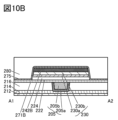
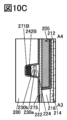
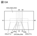
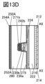
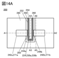
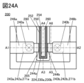
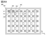
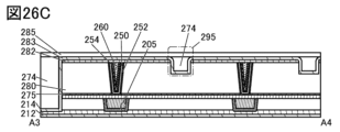
- FIG. 1A is a top view of a semiconductor device which is one embodiment of the present invention.
- 1B to 1D are cross-sectional views of semiconductor devices that are embodiments of the present invention.
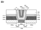
- FIG. 2 is a cross-sectional view of a semiconductor device which is one embodiment of the present invention.
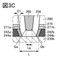
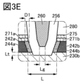
- 3A to 3E are cross-sectional views of semiconductor devices that are embodiments of the present invention.
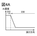
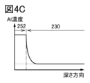
- 4A to 4D are schematic diagrams of aluminum concentration profiles in metal oxides.
- 5A and 5B are cross-sectional views of a semiconductor device that is one embodiment of the present invention.
- 6A and 6B are cross-sectional views of a semiconductor device that is one embodiment of the present invention.
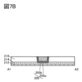
- FIG. 7A is a top view illustrating a method for manufacturing a semiconductor device which is one embodiment of the present invention.
- FIG. 7B to 7D are cross-sectional views illustrating a method for manufacturing a semiconductor device which is one embodiment of the present invention.
- FIG. 8A is a top view illustrating a method for manufacturing a semiconductor device which is one embodiment of the present invention.
- 8B to 8D are cross-sectional views illustrating a method for manufacturing a semiconductor device which is one embodiment of the present invention.
- FIG. 9A is a top view illustrating a method for manufacturing a semiconductor device which is one embodiment of the present invention.
- 9B to 9D are cross-sectional views illustrating a method for manufacturing a semiconductor device which is one embodiment of the present invention.
- FIG. 10A is a top view illustrating a method for manufacturing a semiconductor device which is one embodiment of the present invention.
- FIG. 10B to 10D are cross-sectional views illustrating a method for manufacturing a semiconductor device which is one embodiment of the present invention.
- FIG. 11A is a top view illustrating a method for manufacturing a semiconductor device which is one embodiment of the present invention.
- 11B to 11D are cross-sectional views illustrating a method for manufacturing a semiconductor device which is one embodiment of the present invention.
- FIG. 12A is a top view illustrating a method for manufacturing a semiconductor device which is one embodiment of the present invention.
- 12B to 12D are cross-sectional views illustrating a method for manufacturing a semiconductor device which is one embodiment of the present invention.
- FIG. 13A is a top view illustrating a method for manufacturing a semiconductor device which is one embodiment of the present invention.
- FIG. 13B to 13D are cross-sectional views illustrating a method for manufacturing a semiconductor device which is one embodiment of the present invention.
- FIG. 14A is a top view illustrating a method for manufacturing a semiconductor device which is one embodiment of the present invention.
- 14B to 14D are cross-sectional views illustrating a method for manufacturing a semiconductor device which is one embodiment of the present invention.
- FIG. 15A is a top view illustrating a method for manufacturing a semiconductor device which is one embodiment of the present invention.
- 15B to 15D are cross-sectional views illustrating a method for manufacturing a semiconductor device which is one embodiment of the present invention.
- FIG. 16A is a top view illustrating a method for manufacturing a semiconductor device which is one embodiment of the present invention.
- FIG. 16B to 16D are cross-sectional views illustrating a method for manufacturing a semiconductor device which is one embodiment of the present invention.
- FIG. 17A is a top view illustrating a method for manufacturing a semiconductor device which is one embodiment of the present invention.
- 17B to 17D are cross-sectional views illustrating a method for manufacturing a semiconductor device which is one embodiment of the present invention.
- FIG. 18 is a top view illustrating a microwave processing apparatus according to one embodiment of the present invention.
- FIG. 19 is a schematic cross-sectional view illustrating a microwave processing apparatus according to one embodiment of the present invention.
- FIG. 20 is a cross-sectional schematic diagram illustrating a microwave processing apparatus according to one embodiment of the present invention.
- FIG. 17A is a top view illustrating a method for manufacturing a semiconductor device which is one embodiment of the present invention.
- 17B to 17D are cross-sectional views illustrating a method for manufacturing a semiconductor device which is one embodiment of the present invention.
- FIG. 18 is
- FIG. 21 is a schematic diagram illustrating a microwave processing apparatus according to one embodiment of the present invention.
- FIG. 22A is a top view of a semiconductor device which is one embodiment of the present invention.
- 22B to 22D are cross-sectional views of semiconductor devices that are embodiments of the present invention.
- FIG. 23A is a top view of a semiconductor device which is one embodiment of the present invention.
- 23B to 23D are cross-sectional views of a semiconductor device that is one embodiment of the present invention.
- FIG. 24A is a top view of a semiconductor device which is one embodiment of the present invention.
- 24B to 24D are cross-sectional views of semiconductor devices that are embodiments of the present invention.
- FIG. 25A is a top view of a semiconductor device which is one embodiment of the present invention.
- FIG. 25B to 25D are cross-sectional views of semiconductor devices that are one embodiment of the present invention.
- FIG. 26A is a plan view of a semiconductor device according to one embodiment of the present invention.
- 26B and 26C are cross-sectional views of a semiconductor device that is one embodiment of the present invention.
- 27A and 27B are diagrams illustrating configuration examples of a display device.
- 28A to 28D are circuit diagrams showing configuration examples of display devices.
- 29A to 29D are circuit diagrams showing configuration examples of display devices.
- FIG. 30 is a circuit diagram showing a configuration example of a display device.
- 31A to 31C are diagrams showing configuration examples of display devices.
- 32A to 32F are diagrams showing configuration examples of pixels.
- FIG. 33 is a diagram illustrating a configuration example of a display device.
- FIG. 34 is a diagram illustrating a configuration example of a display device.
- FIG. 35 is a diagram illustrating a configuration example of a display device.
- FIG. 36 is a diagram illustrating a configuration example of a display device.
- 37A to 37F are diagrams showing configuration examples of light-emitting elements.
- 38A to 38C are diagrams showing configuration examples of light-emitting elements.
- 39A to 39D are diagrams showing examples of electronic devices.
- 40A to 40F are diagrams showing examples of electronic devices.
- 41A to 41G are diagrams illustrating examples of electronic devices.
- FIG. 42A is a block diagram illustrating a configuration example of a memory device according to one embodiment of the present invention.
- FIG. 42A is a block diagram illustrating a configuration example of a memory device according to one embodiment of the present invention.
- FIG. 42B is a perspective view illustrating a configuration example of a memory device according to one embodiment of the present invention.
- 43A to 43H are circuit diagrams illustrating configuration examples of memory devices according to one embodiment of the present invention.
- FIG. 44 is a diagram for explaining the etching rate of metal oxide.
- 45A to 45C are diagrams illustrating a method for manufacturing a sample.
- FIG. 46 is a cross-sectional STEM image of a transistor included in the manufactured sample.
- 47A and 47B are schematic cross-sectional views of transistors used for device simulation.
- FIG. 48A is a diagram showing Cg-Vg characteristics obtained by device simulation.
- FIG. 48B is a diagram showing Id-Vg characteristics obtained by device simulation.
- FIG. 49A is a diagram showing Id-Vg characteristics obtained by device simulation.
- FIG. 49B shows the results of Vth estimated from the Id-Vg characteristics.
- FIG. 49C shows the drain current estimated from the Id-Vg characteristics.
- 50A and 50B are cross-sectional STEM images of the prepared sample.
- FIG. 51 shows the Id-Vg characteristics of the transistor.
- FIG. 52 shows a normal probability plot of Vth.
- FIG. 53 is a diagram showing measurement results of cutoff frequencies of transistors.
- FIG. 54A is a diagram for explaining the laminated structure of the laminated film.
- Figures 54B and 54C are the results of SIMS analysis of the prepared samples.
- FIG. 55 is a diagram showing the sheet resistance of the manufactured samples.
- 56A and 56B are the Id-Vg characteristics of the transistor.
- FIG. 57A to 57C are cross-sectional STEM images of transistors included in manufactured samples.
- FIG. 58A is the Id-Vg characteristic of the transistor.
- FIG. 58B shows a normal probability plot of Vth.
- FIG. 59 is a diagram showing the relationship between Hall mobility and carrier concentration of metal oxides.
- 60A to 60D are Id-Vg characteristics of transistors.
- FIG. 61 is a diagram showing the relationship between threshold voltage and field effect mobility in the linear region.
- FIG. 62A is a diagram showing temperature dependence of carrier concentration of a metal oxide.
- FIG. 62B is a diagram showing temperature dependence of Hall mobility of metal oxides.
- top views also referred to as “plan views”
- perspective views also referred to as “plan views”.
- description of some hidden lines may be omitted.
- the ordinal numbers such as first and second are used for convenience and do not indicate the order of steps or the order of stacking. Therefore, for example, “first” can be appropriately replaced with “second” or “third”. Also, the ordinal numbers described in this specification and the like may not match the ordinal numbers used to specify one aspect of the present invention.
- connection relationships other than the connection relationships shown in the drawings or the text are not limited to the predetermined connection relationships, for example, the connection relationships shown in the drawings or the text.
- X and Y are objects (for example, devices, elements, circuits, wiring, electrodes, terminals, conductive films, layers, etc.).
- a transistor is an element having at least three terminals including a gate, a drain, and a source.
- a region in which a channel is formed (hereinafter also referred to as a channel formation region) is provided between the drain (drain terminal, drain region, or drain electrode) and the source (source terminal, source region, or source electrode).
- a current can flow between the source and the drain through the formation region.
- a channel formation region means a region where current mainly flows.
- the function of the source or drain may be switched when using transistors of different polarities or when the direction of current changes in circuit operation. Therefore, in this specification and the like, the terms “source” and “drain” can be used interchangeably in some cases.
- the channel length is, for example, a region in which a semiconductor (or a portion of the semiconductor in which current flows when the transistor is on) overlaps with a gate electrode in a top view of a transistor, or the source length in a channel formation region.
- channel lengths in one transistor do not always have the same value in all regions. That is, the channel length of one transistor may not be fixed to one value. Therefore, in this specification, the channel length is any one value, maximum value, minimum value, or average value in the channel forming region.
- the channel width is, for example, a region in which a semiconductor (or a portion of the semiconductor in which current flows when the transistor is on) overlaps with a gate electrode in a top view of a transistor, or a channel formation region in the channel length direction.
- a channel width in a region where a channel is actually formed (hereinafter also referred to as an “effective channel width”) and a channel width shown in a top view of a transistor ( hereinafter also referred to as “apparent channel width”) may be different.
- the effective channel width becomes larger than the apparent channel width, and its influence cannot be ignored.
- the proportion of the channel formation region formed on the side surface of the semiconductor may be large. In that case, the effective channel width is larger than the apparent channel width.
- channel width may refer to the apparent channel width.
- channel width may refer to the effective channel width.
- the channel length, channel width, effective channel width, or apparent channel width can be determined by analyzing cross-sectional TEM images, for example.
- impurities in a semiconductor refer to, for example, substances other than the main components that constitute the semiconductor.
- an element whose concentration is less than 0.1 atomic percent can be said to be an impurity.
- the inclusion of impurities may cause, for example, an increase in the defect level density of the semiconductor, a decrease in crystallinity, and the like.
- impurities that change the characteristics of the semiconductor include, for example, group 1 elements, group 2 elements, group 13 elements, group 14 elements, group 15 elements, and oxide semiconductors.
- transition metals other than the main component such as hydrogen, lithium, sodium, silicon, boron, phosphorus, carbon, and nitrogen.
- water may also function as an impurity.
- oxygen vacancies also referred to as V 2 O 3
- silicon oxynitride contains more oxygen than nitrogen as its composition.
- Silicon nitride oxide contains more nitrogen than oxygen in its composition.
- insulator can be replaced with an insulating film or an insulating layer.
- conductor can be replaced with a conductive film or a conductive layer.
- semiconductor can be interchanged with a semiconductor film or a semiconductor layer.
- parallel means a state in which two straight lines are arranged at an angle of -10 degrees or more and 10 degrees or less. Therefore, the case of ⁇ 5 degrees or more and 5 degrees or less is also included.
- substantially parallel means a state in which two straight lines are arranged at an angle of -30 degrees or more and 30 degrees or less.
- Perfect means that two straight lines are arranged at an angle of 80 degrees or more and 100 degrees or less. Therefore, the case of 85 degrees or more and 95 degrees or less is also included.
- substantially perpendicular means a state in which two straight lines are arranged at an angle of 60 degrees or more and 120 degrees or less.
- a metal oxide is a metal oxide in a broad sense.
- Metal oxides are classified into oxide insulators, oxide conductors (including transparent oxide conductors), oxide semiconductors (also referred to as oxide semiconductors or simply OSs), and the like.
- oxide semiconductors also referred to as oxide semiconductors or simply OSs
- an OS transistor can be referred to as a transistor including a metal oxide or an oxide semiconductor.
- the term “normally-off” means that the drain current per 1 ⁇ m of the channel width flowing through the transistor when no potential is applied to the gate or when a ground potential is applied to the gate is 1 ⁇ 10 ⁇ 1 at room temperature. 20 A or less, 1 ⁇ 10 ⁇ 18 A or less at 85° C., or 1 ⁇ 10 ⁇ 16 A or less at 125° C.
- Voltage is a potential difference from a reference potential.
- the reference potential is ground potential
- “voltage” can be replaced with “potential”. Note that the ground potential does not necessarily mean 0V.
- the potential is relative, and when the reference potential changes, the potential applied to the wiring, the potential applied to the circuit, etc., and the potential output from the circuit etc. also change.
- the heights are the same or approximately the same” refers to a configuration in which the heights from a reference surface (for example, a flat surface such as a substrate surface) are equal in cross-sectional view.
- planarization processing typically CMP processing
- CMP processing may expose the surface of a single layer or multiple layers.
- the surfaces to be CMP-processed have the same height from the reference surface.
- the heights of the layers may differ depending on the processing equipment, processing method, or material of the surface to be processed during the CMP processing. In this specification and the like, this case is also treated as "the height matches or roughly matches".
- the height of the top surface of the first layer and the height of the second layer When the difference in height from the upper surface of the layer is 20 nm or less, it is also said that the heights are the same or approximately the same.
- the ends match or roughly match means that at least part of the outline overlaps between the laminated layers when viewed from the top.
- the upper layer and the lower layer may be processed with the same mask pattern, or partially with the same mask pattern.
- the contours do not overlap, and the upper contour may be positioned inside the lower contour, or the upper contour may be positioned outside the lower contour. “match or approximate match”.
- a semiconductor device which is one embodiment of the present invention includes a transistor.
- FIG. 1A-1D are top and cross-sectional views of a semiconductor device having a transistor 200.
- FIG. 1A is a top view of the semiconductor device.
- 1B to 1D are cross-sectional views of the semiconductor device.
- FIG. 1B is a cross-sectional view of the portion indicated by the dashed-dotted line A1-A2 in FIG. 1A, and is also a cross-sectional view of the transistor 200 in the channel length direction.
- FIG. 1C is a cross-sectional view of the portion indicated by the dashed-dotted line A3-A4 in FIG.
- FIG. 1A is also a cross-sectional view of the transistor 200 in the channel width direction.
- FIG. 1D is sectional drawing of the site
- a semiconductor device of one embodiment of the present invention includes an insulator 212 over a substrate (not shown), an insulator 214 over the insulator 212, a transistor 200 over the insulator 214, and an insulator 280 over the transistor 200. , insulator 282 on insulator 280 , insulator 283 on insulator 282 , insulator 274 on insulator 283 , insulator 283 and insulator 285 on insulator 274 .
- the insulator 212, the insulator 214, the insulator 280, the insulator 282, the insulator 283, the insulator 285, the insulator 274, and the insulator 285 function as interlayer films.
- an insulator 241a is provided in contact with a side surface of the conductor 240a
- an insulator 241b is provided in contact with a side surface of the conductor 240b.
- a conductor 246a electrically connected to the conductor 240a is provided over the insulator 285 and the conductor 240a
- an electric conductor 240b is provided over the insulator 285 and the conductor 240b.
- a conductor 246b is provided connecting to the .
- the insulator 283 is in contact with part of the top surface of the insulator 214 , the side surfaces of the insulator 280 , and the side surfaces and top surface of the insulator 282 .
- An insulator 241a is provided in contact with the inner wall of the opening of the insulator 280, the insulator 282, the insulator 283, and the insulator 285, and the conductor 240a is provided in contact with the side surface of the insulator 241a.
- An insulator 241b is provided in contact with the inner wall of the opening of the insulator 280, the insulator 282, the insulator 283, and the insulator 285, and the conductor 240b is provided in contact with the side surface of the insulator 241b.
- Each of the insulators 241a and 241b has a structure in which a first insulator is provided in contact with the inner wall of the opening, and a second insulator is provided inside.
- the conductor 240a has a structure in which a first conductor is provided in contact with the side surface of the insulator 241a and a second conductor is provided inside.
- the conductor 240b has a structure in which a first conductor is provided in contact with the side surface of the insulator 241b and a second conductor is provided inside.
- the height of the top surface of the conductor 240a and the height of the top surface of the insulator 285 in the region overlapping with the conductor 246a can be made approximately the same.
- the top surface of the conductor 240b and the top surface of the insulator 285 in the region overlapping with the conductor 246b can be approximately the same height.
- the insulator 241a and the insulator 241b each have a structure in which a first insulator and a second insulator are stacked, but the present invention is not limited to this.
- each of the insulator 241a and the insulator 241b may be provided as a single layer or a stacked structure of three or more layers.
- the conductor 240a and the conductor 240b each have a structure in which a first conductor and a second conductor are stacked, but the present invention is not limited to this.
- each of the conductor 240a and the conductor 240b may be provided as a single layer or a laminated structure of three or more layers. When the structure has a laminated structure, an ordinal number may be assigned in order of formation for distinction.
- the transistor 200 includes an insulator 216 over an insulator 214, conductors 205 (a conductor 205a and a conductor 205b) embedded in the insulator 216, Insulator 216 and insulator 222 over conductor 205, insulator 224 over insulator 222, oxide 230a over insulator 224, oxide 230b over oxide 230a, and oxide 230b Conductors 242a and 242b, insulator 271a over conductor 242a, insulator 271b over conductor 242b, and oxide 230b between conductors 242a and 242b.
- the transistor 200 also includes an insulator 244 a positioned between the conductor 242 a and the insulator 252 and an insulator 244 b positioned between the conductor 242 b and the insulator 252 .
- oxide 230a and the oxide 230b may be collectively referred to as the oxide 230 below.
- the conductor 242a and the conductor 242b are collectively referred to as the conductor 242 in some cases.
- the insulator 271a and the insulator 271b are collectively referred to as the insulator 271 .
- the insulator 280 is located on the insulator 275 . Therefore, it can be said that the insulator 280 is positioned above the conductors 242a and 242b. Insulator 280 and insulator 275 are provided with openings down to oxide 230b. In other words, it can be said that the opening has a region between the conductor 242a and the conductor 242b and overlapping with the oxide 230b. In addition, it can be said that the insulator 275 has an opening that overlaps with the opening of the insulator 280 . An insulator 252, an insulator 250, an insulator 254, and a conductor 260 are arranged in the opening.
- the conductor 260 has a region overlapping with the oxide 230b with the insulators 252, 250, and 254 interposed therebetween.
- a conductor 260, an insulator 252, an insulator 250, and an insulator 254 are provided between the insulator 271a and the conductor 242a and the insulator 271b and the conductor 242b. is provided.
- the insulator 254 has a region in contact with the side surface of the conductor 260 and a region in contact with the bottom surface of the conductor 260 .
- the conductor 260 functions as a first gate (also called top gate) electrode, and the conductor 205 functions as a second gate (also called back gate) electrode.
- insulators 252, 250, and 254 function as a first gate insulator
- insulators 222 and 224 function as a second gate insulator.
- the gate insulator is sometimes called a gate insulating layer or a gate insulating film.
- the conductor 242a functions as one of the source electrode and the drain electrode
- the conductor 242b functions as the other of the source electrode and the drain electrode. At least part of the region of the oxide 230 overlapping with the conductor 260 functions as a channel formation region.
- the thickness of the gate insulator In order to miniaturize or increase the integration of transistors, it is necessary to reduce the thickness of the gate insulator. However, as the gate insulator becomes thinner, the parasitic capacitance between the source electrode and the gate electrode and the parasitic capacitance between the drain electrode and the gate electrode increase. , and leakage current between the drain electrode and the gate electrode increases.
- the insulator 244a is provided between the conductor 242a functioning as one of the source electrode and the drain electrode and the conductor 260 functioning as the top gate electrode.
- An insulator 244 b is provided between the functional conductor 242 b and the conductor 260 .
- a metal oxide functioning as a semiconductor (hereinafter also referred to as an oxide semiconductor) is preferably used for the oxide 230 including the channel formation region.
- the bandgap of the metal oxide that functions as a semiconductor is preferably 2 eV or more, more preferably 2.5 eV or more.
- the off-state current of the transistor can be reduced by using a metal oxide with a large bandgap.
- the channel forming region has a reduced carrier concentration and is preferably i-type or substantially i-type, and the source and drain regions have a high carrier concentration and are preferably n-type.
- a semiconductor device having favorable electrical characteristics can be provided. Note that at least part of the channel formation region of the oxide 230 overlaps with the conductor 260 . In other words, the channel formation region is provided in a region between the conductors 242a and 242b. One of the source region and the drain region is provided to overlap with the conductor 242a, and the other of the source region and the drain region is provided to overlap with the conductor 242b.
- a transistor including an oxide semiconductor tends to have electrical characteristics that fluctuate, and reliability may be degraded.
- a defect in which hydrogen is added to an oxygen vacancy (hereinafter sometimes referred to as VOH ) may be formed to generate an electron serving as a carrier. Therefore, if oxygen vacancies are included in the channel formation region in the oxide semiconductor, the transistor has normally-on characteristics (a channel exists even if no voltage is applied to the gate electrode, and a current flows through the transistor). easy to become. Therefore, impurities, oxygen vacancies, and VOH are preferably reduced as much as possible in the channel formation region in the oxide semiconductor.
- an insulator containing oxygen that is released by heating (hereinafter sometimes referred to as excess oxygen) is provided in the vicinity of the oxide semiconductor, and heat treatment is performed so that the oxide semiconductor is converted from the insulator.
- Oxygen can be supplied and oxygen vacancies and VOH can be reduced.
- the on-state current of the transistor may decrease or the field-effect mobility may decrease.
- variations in the amount of oxygen supplied to the source region or the drain region within the substrate surface cause variations in the characteristics of the semiconductor device having transistors.
- oxygen supplied from the insulator to the oxide semiconductor diffuses into a conductor such as a gate electrode, a source electrode, or a drain electrode, the conductor is oxidized and the conductivity is impaired. It may adversely affect the electrical characteristics and reliability of the transistor.
- oxygen vacancies and VOH are preferably reduced in the channel formation region. Therefore, it is preferable to supply oxygen to the channel formation region and prevent an excessive amount of oxygen from being supplied to the source region and the drain region. Furthermore, it is preferable to suppress the diffusion of hydrogen into the channel formation region.
- An insulator that easily transmits oxygen is preferably used as the insulator 250 in order to supply oxygen to the channel formation region.
- An insulator containing excess oxygen is preferably used as the insulator 280 . With such a structure, oxygen contained in the insulator 280 can be supplied to the channel formation region of the oxide 230 through the insulator 250 .
- the channel forming region of oxide 230 can be i-type or substantially i-type.
- the insulator 250 for example, silicon oxide, silicon oxynitride, silicon oxide to which fluorine is added, silicon oxide to which carbon is added, silicon oxide to which carbon and nitrogen are added, silicon oxide having vacancies, or the like can be used.
- silicon oxide and silicon oxynitride are preferable because they are stable against heat.
- the insulator 250 contains at least oxygen and silicon.
- the concentration of impurities such as water and hydrogen in the insulator 250 is reduced.
- the thickness of the insulator 250 is preferably 0.5 nm or more and 20 nm or less, more preferably 1 nm or more and 15 nm or less.
- the thickness of the insulator 250 is preferably 0.5 nm or more and 10 nm or less, more preferably 0.5 nm or more and 5 nm or less. is more preferred.
- the insulator 250 may have at least a portion of the region with the film thickness as described above.
- the insulator 250 is provided in contact with the upper surface of the insulator 252 .
- the insulator 280 is, for example, an oxide containing silicon, such as silicon oxide, silicon oxynitride, fluorine-added silicon oxide, carbon-added silicon oxide, carbon- and nitrogen-added silicon oxide, or silicon oxide having vacancies. is preferably used.
- silicon oxide and silicon oxynitride are preferable because they are thermally stable.
- a material such as silicon oxide, silicon oxynitride, or silicon oxide having vacancies is preferable because a region containing oxygen that is released by heating can be easily formed.
- the insulator 280 functions as an interlayer film, it preferably has a low dielectric constant. By using a material with a low dielectric constant as the interlayer film, the parasitic capacitance generated between wirings can be reduced.
- the silicon-containing oxides described above are preferred because they are materials with low dielectric constants.
- the concentration of impurities such as water and hydrogen in the insulator 280 is reduced.
- the insulator 280 is provided on the insulator 275 and has openings in regions where the insulator 252, the insulator 250, the insulator 254, and the conductor 260 are provided. Also, the upper surface of the insulator 280 may be flattened.
- the source region and the drain region are excessively oxidized through the channel formation region, and the on-current of the transistor 200 is lowered or the field effect mobility is reduced. may cause a decrease in
- an insulator 252 having a barrier property against oxygen is preferably provided between the insulator 250 and the oxide 230b.
- the insulator 252 is provided in contact with the bottom surface of the insulator 250, the top surface of the oxide 230b, and the side surfaces of the oxide 230b. Since the insulator 252 has a barrier property against oxygen, oxygen contained in the insulator 250 can be supplied to the channel formation region, and excessive supply of oxygen contained in the insulator 250 to the channel formation region can be suppressed. Therefore, excessive supply of oxygen to the source region and the drain region through the channel formation region can suppress a decrease in on-state current or a decrease in field-effect mobility of the transistor 200 .
- the insulator 252 is provided between the insulators 280 and has a region in contact with the sidewall of the opening of the insulator 280 . With such a structure, oxygen contained in the insulator 280 can be supplied to the insulator 250 and excessive supply of oxygen contained in the insulator 280 to the insulator 250 can be suppressed.
- an insulator containing oxides of one or both of aluminum and hafnium is preferable to use as the insulator 252 .
- the insulator aluminum oxide, hafnium oxide, an oxide containing aluminum and hafnium (hafnium aluminate), an oxide containing hafnium and silicon (hafnium silicate), or the like can be used.
- aluminum oxide is used as the insulator 252 .
- the insulator 252 contains at least oxygen and aluminum.
- the insulator 252 may be less permeable to oxygen than the insulator 250, for example.
- the insulator 252 for example, a material that is less permeable to oxygen than the insulator 250 may be used.
- the insulator 252 may be formed using magnesium oxide, gallium oxide, gallium zinc oxide, indium gallium zinc oxide, or the like.
- the film thickness of the insulator 252 is preferably thin. This is because if the insulator 252 is too thick, the amount of oxygen supplied to the oxide 230 through the insulator 250 is reduced.
- the thickness of the insulator 252 is 0.1 nm to 5.0 nm, preferably 0.5 nm to 3.0 nm, more preferably 1.0 nm to less than 3.0 nm.
- at least part of the insulator 252 may have a region with the thickness as described above.
- the insulator 252 preferably has a region with a thickness smaller than that of the insulator 250 .
- at least part of the insulator 252 may have a region thinner than the insulator 250 .
- the ALD method includes a thermal ALD (thermal ALD) method in which a precursor and a reactant react with only thermal energy, a PEALD (plasma enhanced ALD) method using a plasma-excited reactant, and the like.
- thermal ALD thermal ALD
- PEALD plasma enhanced ALD
- film formation can be performed at a lower temperature by using plasma, which is preferable in some cases.
- the ALD method can deposit atoms one layer at a time, it is possible to form extremely thin films, to form structures with a high aspect ratio, to form films with few defects such as pinholes, and to improve coverage. There are effects such as excellent film formation and low temperature film formation. Therefore, the insulator 252 can be formed with a thin film thickness as described above with good coverage on the side surfaces of the opening formed in the insulator 280 or the like.
- a film formed by the ALD method may contain more impurities such as carbon than films formed by other film formation methods.
- quantification of impurities secondary ion mass spectrometry (SIMS: Secondary Ion Mass Spectrometry), X-ray photoelectron spectroscopy (XPS: X-ray Photoelectron Spectroscopy), or Auger electron spectroscopy (AES: Auger Electron Spectroscopy) can be performed using
- the insulator 252 By reducing the film thickness of the insulator 252, miniaturization of the transistor 200 can be achieved. This is because the insulator 252 is provided in an opening formed in the insulator 280 or the like together with the insulator 254 , the insulator 250 , and the conductor 260 . With such a structure, a semiconductor device that can be miniaturized or highly integrated can be provided.
- the insulator 252 is provided between the insulator 250 and the conductor 242a and between the insulator 250 and the conductor 242b.
- the side surface of the conductor 242a is oxidized to form an insulator 244a.
- the sides of conductor 242b are oxidized to form insulator 244b.
- the transistor 200 has an insulator 244 a located between the conductor 242 a and the insulator 252 and an insulator 244 b located between the conductor 242 b and the insulator 252 .
- the lengths of the insulators 244a and 244b in the channel length direction can be controlled. For example, by increasing the thickness of the insulator 252, the amount of oxygen contained in the insulator 250 that diffuses into the conductors 242a and 242b is reduced, and the side surfaces of the conductors 242a and 242b are oxidized. can be suppressed, and the lengths of the insulators 244a and 244b in the channel length direction can be reduced. Accordingly, a decrease in on-state current or a decrease in field-effect mobility of the transistor 200 can be suppressed.
- the insulator 244a and the insulator 244b are self-aligned (self-aligned) when the conductor 242a and the conductor 242b are formed or in a process after the conductor 242a and the conductor 242b are formed. (also called alignment). Therefore, the parasitic capacitance between the conductors 242a and 260 and the parasitic capacitance between the conductors 242b and 260 can be reduced in a self-aligning manner.
- the insulator 244a contains an element included in the conductor 242a and oxygen.
- the insulator 244b contains an element included in the conductor 242b and oxygen.
- the insulators 244a and 244b each contain the metal element and oxygen.
- the insulators 244a and 244b each contain the metal element, oxygen, and nitrogen. have.
- An insulator having a function of suppressing diffusion of hydrogen is preferably provided near the oxide 230 in order to suppress diffusion of hydrogen into the channel formation region.
- the insulators are the insulators 252 and 254, for example.
- Aluminum oxide which can be suitably used as the insulator 252, has a function of suppressing diffusion of hydrogen (for example, at least one of hydrogen atoms and hydrogen molecules). Therefore, impurities such as hydrogen contained in the insulator 250 can be prevented from diffusing into the oxide 230 .
- the insulator 252 may be less permeable to hydrogen than the insulator 250, for example. Further, the insulator 252 may be made of a material that is less permeable to hydrogen than the insulator 250, for example.
- the insulator 254 preferably has a barrier property against hydrogen. Accordingly, impurities such as hydrogen contained in the conductor 260 can be prevented from diffusing into the insulator 250 and the oxide 230 .
- the insulator 254 for example, silicon nitride deposited by a PEALD method may be used. In this case, insulator 254 comprises at least nitrogen and silicon.
- the insulator 254 for example, aluminum oxide, magnesium oxide, hafnium oxide, gallium oxide, indium gallium zinc oxide, silicon nitride oxide, or the like may be used. Note that the insulator 254 may be less permeable to hydrogen than the insulator 250, for example.
- a material that is less permeable to hydrogen than the insulator 250 may be used.
- the insulator 254 may further have barrier properties against oxygen. Insulator 254 is provided between insulator 250 and conductor 260 . Therefore, oxygen contained in the insulator 250 can be prevented from diffusing into the conductor 260, and oxidation of the conductor 260 can be suppressed. In addition, reduction in the amount of oxygen supplied to the oxide 230 can be suppressed. Note that the insulator 254 may be less permeable to oxygen than the insulator 250, for example. For the insulator 254, for example, a material that is less permeable to oxygen than the insulator 250 may be used.
- the thickness of the insulator 254 is preferably thin.
- the insulator 254 has a thickness of 0.1 nm to 5.0 nm, preferably 0.5 nm to 3.0 nm, more preferably 1.0 nm to 3.0 nm. In this case, at least part of the insulator 254 may have a region with the thickness as described above. Further, the thickness of the insulator 254 is preferably thinner than the thickness of the insulator 250 . In this case, at least part of the insulator 254 may have a region thinner than the insulator 250 .
- FIG. 2 shows an enlarged view of the vicinity of the channel forming region in FIG. 1B.
- the length of the insulator 244a in the channel length direction is defined as a length D1.
- the length D1 is also the distance from the conductor 242a to the insulator 252 in a cross-sectional view in the channel length direction.
- the length D1 is also the distance from the side surface of the conductor 242a to the surface of the insulator 252 in contact with the insulator 244a.
- the length D1 is the difference between the position of the interface between the conductor 242 a and the insulator 244 a and the position of the interface between the insulator 244 a and the insulator 252 .
- the length of the insulator 244b in the channel length direction matches or substantially matches the length D1.
- the length D1 is preferably 1 nm or more, 3 nm or more, or 5 nm or more, and 20 nm or less, 15 nm or less, or 10 nm or less.
- the length D1 is preferably greater than or equal to the film thickness of the insulator 252 and less than or equal to the distance from the conductor 260 to the oxide 230 .
- the distance from the conductor 260 to the oxide 230b refers to, for example, the distance from the bottom surface of the conductor 260a to the top surface of the oxide 230b in a cross-sectional view in the channel length direction.
- the distance from the conductor 260 to the oxide 230 b is also the sum of the thicknesses of the insulators 252 , 250 , and 254 .
- the distance from the conductor 260 to the oxide 230b can be said to be the physical thickness of the first gate insulator.
- the length D1 can sometimes be measured by observing the cross-sectional shape of the insulator 244a and its periphery using a transmission electron microscope (TEM) or the like.
- TEM transmission electron microscope
- the length D1 may be calculated by performing line analysis of the composition of the insulator 244a and its surroundings by energy dispersive X-ray spectroscopy (EDX). For example, as a method of calculating the length D1, EDX line analysis is first performed with the channel length direction as the depth direction. Next, in the profile of the quantitative value of each element in the depth direction obtained by the analysis, the depth (position) of the interface between the insulator 244a and the insulator 252 is the main component of the insulator 252, and , the depth at which the quantified value of the element that is not the main component of the conductor 242a is half the value. Further, the depth (position) of the interface between the conductor 242a and the insulator 244a is set to the depth at which the quantitative value of oxygen is half the value. From the above, the length D1 can be calculated.
- EDX line analysis is first performed with the channel length direction as the depth direction.
- the oxide 230b includes a region 230bc functioning as a channel formation region of the transistor 200, and regions 230ba and 230bb functioning as a source region or a drain region and provided to sandwich the region 230bc. have. At least a portion of the region 230bc overlaps the conductor 260 . In other words, the region 230bc is provided in a region between the conductors 242a and 242b. The region 230ba is provided so as to overlap with the conductor 242a, and the region 230bb is provided so as to overlap with the conductor 242b.
- region 230bc has less oxygen vacancies or a lower impurity concentration than the regions 230ba and 230bb, and is therefore a high resistance region with a low carrier concentration.
- region 230bc can be said to be i-type (intrinsic) or substantially i-type.
- the regions 230ba and 230bb have a large amount of oxygen deficiency or a high concentration of impurities such as hydrogen, nitrogen, and metal elements, so that the carrier concentration is increased and the resistance is lowered. That is, the regions 230ba and 230bb are n-type regions having a higher carrier concentration and a lower resistance than the region 230bc.
- the carrier concentration of the region 230bc is preferably 1 ⁇ 10 18 cm ⁇ 3 or less, more preferably less than 1 ⁇ 10 17 cm ⁇ 3 , and less than 1 ⁇ 10 16 cm ⁇ 3 is more preferably less than 1 ⁇ 10 13 cm ⁇ 3 , even more preferably less than 1 ⁇ 10 12 cm ⁇ 3 .
- the lower limit of the carrier concentration of the region 230bc functioning as a channel forming region is not particularly limited, but can be, for example, 1 ⁇ 10 ⁇ 9 cm ⁇ 3 .
- a region 230bd is formed in the oxide 230b below the insulator 244a.
- the region 230bd has a carrier concentration equal to or lower than that of the region 230ba and equal to or higher than that of the region 230bc. Since the region 230bd is located between the regions 230bc and 230ba, it functions as a junction region or an offset region between the regions 230bc and 230ba.
- the region 230bd may have a hydrogen concentration equal to or lower than that of the region 230ba and equal to or higher than that of the region 230bc.
- transistor 200 has insulator 244b to form region 230be in oxide 230b under insulator 244b.
- Region 230be like region 230bd, functions as a junction region or offset region between regions 230bc and 230bb.
- region 230bd since the region 230bd is located below the insulator 244a, oxygen contained in the insulator 250 or the like may be supplied to the region 230bd through the insulator 244a. Therefore, the region 230bd may have oxygen vacancies equal to or less than those of the regions 230ba and equal to or greater than those of the regions 230bc. Similarly, region 230be may have oxygen vacancies equal to or less than those of region 230bb and equal to or greater than those of region 230bc.
- FIG. 2 shows an example in which the regions 230ba, 230bb, 230bc, 230bd, and 230be are formed in the oxide 230b
- the present invention is not limited to this.
- each of the above regions may be formed up to oxide 230a as well as oxide 230b.
- the concentrations of metal elements and impurity elements such as hydrogen and nitrogen detected in each region are not limited to stepwise changes for each region, and may change continuously within each region. In other words, it is sufficient if the concentration of impurity elements such as hydrogen and nitrogen is reduced in a region closer to the channel formation region.
- the insulator 252 is provided in contact with the top and side surfaces of the oxide 230b, the side surfaces of the oxide 230a, the side surfaces of the insulator 224, and the top surface of the insulator 222. That is, regions of the oxides 230a and 230b, and the insulator 224 overlapping with the conductor 260 are covered with the insulator 252 in the cross section in the channel width direction.
- the insulator 252 has a region in contact with the side surface of the insulator 271a, a region in contact with the side surface of the insulator 271b, and a region in contact with the side wall of the opening of the insulator 275.
- the region 230bc functioning as a channel forming region can be i-type or substantially i-type, and the regions 230ba and 230bb functioning as source or drain regions can be n-type.
- the parasitic capacitance between the conductor 260 and the conductor 242a and the parasitic capacitance between the conductor 260 and the conductor 242b can be reduced in a self-aligning manner. Therefore, a semiconductor device having good electrical characteristics can be provided. Further, with the above structure, even if the semiconductor device is miniaturized or highly integrated, it can have good electrical characteristics.
- the gate length is 20 nm or less, 15 nm or less, 10 nm or less, or 7 nm or less, and is 1 nm or more, 3 nm or more, or 5 nm or more. Note that the gate length will be described later.
- miniaturization of the transistor 200 can improve high-frequency characteristics. Specifically, the cutoff frequency can be improved.
- the cutoff frequency of the transistor can be, for example, 50 GHz or higher, or 100 GHz or higher in a room temperature environment.
- the insulators 252 and 250 each contain oxygen, and the insulators 250 and 250 contain oxygen. Insulators 254 each comprise silicon. Since the layers in contact with each other have a common element as a main component, it is possible to reduce the defect level density at the interface between the layers. Therefore, carrier traps and the like due to the defect level are suppressed, and the transistor 200 and the semiconductor device with favorable characteristics and high reliability can be manufactured.
- the insulator 254 and the conductor 260a each contain nitrogen. With such a structure, the transistor 200 and the semiconductor device with favorable characteristics and high reliability can be manufactured as described above.
- the oxide 230b contains oxygen as its main component, the density of defect states at the interface between the oxide 230b and the insulator 252 can be reduced. Therefore, carrier traps and the like due to the defect level are suppressed, and the transistor 200 and the semiconductor device with favorable characteristics and high reliability can be manufactured.
- the bottom surface of the conductor 260a is preferably positioned between the bottom surface and the top surface of the conductor 242a.
- Such a structure makes it easier for the electric field of the conductor 260 to act on the channel formation region of the oxide 230b. Therefore, the on current of the transistor 200 can be increased and the frequency characteristics can be improved.
- the bottom surface of the conductor 260a may be lower than the bottom surface of the conductor 242a in a cross-sectional view in the channel length direction depending on the thickness of the gate insulator, the amount of removal of the upper portion of the oxide 230b, or the like. Alternatively, it may be located above the upper surface of the conductor 242a.
- FIG. 3A is a cross-sectional view of the transistor 200 in the channel length direction.
- insulator 252, insulator 250, and insulator 254 function as the first gate insulator.
- the insulator 252, the insulator 250, and the insulator 254 may be collectively referred to as an insulator 256.
- insulator 256 has insulator 252 , insulator 250 over insulator 252 , and insulator 254 over insulator 250 .
- Insulator 256 also functions as a first gate insulator.
- FIG. 3B shows a cross-sectional view in which the insulator 252, the insulator 250, and the insulator 254 included in FIG. 3A are replaced with the insulator 256.
- FIG. 3B the conductor 260 is shown as a single layer for simplification of the drawing. As described above, the conductor 260 may have a laminated structure of the conductors 260a and 260b, or may have a laminated structure of three or more layers.
- the width Lg shown in FIGS. 3A and 3B is the width of the bottom surface of the conductor 260 in the region overlapping with the oxide 230b in a cross-sectional view in the channel length direction.
- the bottom surface of the conductor 260 in the region overlapping with the oxide 230b in a cross-sectional view in the channel length direction may simply be referred to as the bottom surface of the conductor 260 in the region overlapping with the oxide 230b. That is, the bottom surface of the conductor 260 in the region overlapping with the oxide 230b, which will be described later, can be read as the bottom surface of the conductor 260 in the region overlapping with the oxide 230b in a cross-sectional view in the channel length direction. .
- the gate length is the length of the gate electrode in the direction in which carriers move inside the channel formation region during transistor operation, and refers to the width of the bottom surface of the gate electrode in the top view of the transistor.
- the gate length is the width of the bottom surface of the conductor 260 in the region overlapping with the oxide 230b in a cross-sectional view in the channel length direction. That is, the gate length becomes the width Lg shown in FIGS. 3A and 3B.
- the conductor 260 is provided inside the openings of the insulators 275 and 280 .
- the sidewall of the opening is perpendicular to the substrate surface or inclined with respect to the substrate surface.
- the minimum width of the conductor 260 in the region overlapping with the oxide 230b is the width Lg. Therefore, it can be said that the conductor 260 has a region with a width Lg in a cross-sectional view in the channel length direction.
- the bottom surface of the conductor 260 in the region overlapping with the oxide 230b preferably has a flat region. As shown in FIGS. 3A and 3B, if the bottom surface of conductor 260 in the region overlapping oxide 230b has a flat area, width Lg is the width of the flat area. Since the bottom surface of the conductor 260 in the region overlapping with the oxide 230 b has a flat region, an electric field can be uniformly generated in the channel formation region of the oxide 230 .
- FIGS. 3A and 3B show a structure in which the bottom surface of the conductor 260 in the region overlapping with the oxide 230b has a flat region, the present invention is not limited to this.
- the bottom surface of the conductor 260 in the region overlapping with the oxide 230b may have a curve when viewed in cross section in the channel length direction.
- FIG. 3C is a cross-sectional view of the transistor 200 in the channel length direction.
- the bottom surface of conductor 260 in the region overlapping oxide 230b may have flat regions and curved regions. Note that the curved regions are located at both ends of the bottom surface.
- the point where the curve of the bottom surface on the side of the conductor 242a contacts the side surface of the conductor 260 on the side of the conductor 242a is defined as a point Qa.
- a point Qb is a point where the curve of the bottom surface on the side of the conductor 242b contacts the side surface of the conductor 260 on the side of the conductor 242b.
- the width Lg is the length of the line segment connecting the points Qa and Qb.
- FIG. 3D shows a modification of the transistor 200 shown in FIG. 3B.
- FIG. 3D is a cross-sectional view of the transistor 200 in the channel length direction.
- conductor 260 may have an arcuate bottom surface, as shown in FIG. 3D.
- the arc has a center of curvature P located within the conductor 260 and a radius r.
- the width Lg is the width of the region where the conductor 260 overlaps with the straight line that includes the center of curvature P and is parallel to the bottom surface of the oxide 230b in a cross-sectional view in the channel length direction.
- the width Lg is twice the radius r.
- 3D is a straight line that includes the center of curvature P and is parallel to the bottom surface of the oxide 230b.
- the width Lg shown in FIG. 3C may be applied as the gate length of the shape. That is, the width Lg may be calculated by determining the points Qa and Qb for the shape of the bottom surface of the conductor 260 shown in FIG. 3D.
- the width Lg shown in FIG. 3D may be applied as the gate length of the shape. That is, the width Lg may be calculated by determining the center of curvature P for the shape of the bottom surface of the conductor 260 shown in FIG. 3C.
- the insulator 244a has lower conductivity than the conductor 242a, and the insulator 244b has lower conductivity than the conductor 242b. Therefore, when the transistor 200 has insulators 244a and 244b, the distance between the bottom ends of the conductors 242a and 242b can be considered as the channel length, as shown in FIGS. 3A to 3D. can. That is, the channel length can be increased by forming the insulator 244a and the insulator 244b. Therefore, the source-drain breakdown voltage of the transistor 200 can be improved, and a highly reliable transistor can be realized. Therefore, good electrical characteristics can be obtained even if the transistor is miniaturized.
- a distance L is the distance between the lower end of the conductor 242a and the lower end of the conductor 242b.
- the channel length is set according to the material used for the conductor 260, the gate length, and the material and film thickness used for the first gate insulator.
- the channel length may be, for example, 60 nm or less, 50 nm or less, 40 nm or less, or 30 nm or less, and may be 5 nm or more, 10 nm or more, 15 nm or more, or 20 nm or more. .
- the length D1 of the insulator 244a in the channel length direction is preferably smaller than the width Lg and is preferably within any of the above ranges. With such a structure, the transistor 200 can have favorable electrical characteristics even when the gate length is in any of the above ranges. Note that if the width Lg is very small (for example, less than 5 nm), the length D1 may be greater than the width Lg.
- the upper portion of the oxide 230b in the region overlapping the openings may be removed.
- the film thickness of the region of the oxide 230b overlapping the conductor 260 is smaller than the film thickness of the region of the oxide 230b overlapping the conductor 242a.
- the transistor 200 shown in FIG. 3E is a modification of the transistor 200 shown in FIG. 3B.
- FIG. 3E is a cross-sectional view of the transistor 200 in the channel length direction.
- the difference between the thickness of the oxide 230b in the region overlapping the conductor 260 and the thickness of the oxide 230b in the region overlapping the conductor 242a is defined as a difference Lt. If the difference Lt is small, the distance L may be regarded as the channel length.
- a highly reliable semiconductor device can be provided.
- a semiconductor device having favorable electrical characteristics can be provided.
- a semiconductor device that can be miniaturized or highly integrated can be provided.
- a semiconductor device that has favorable electrical characteristics and can be miniaturized or highly integrated can be provided.
- microwave treatment is performed in an atmosphere containing oxygen in a state where the conductors 242a and 242b are provided over the oxide 230b, so that oxygen vacancies in the region 230bc and VOH are reduced. Plan. Note that the microwave treatment will be described later in detail in ⁇ Manufacturing Method of Semiconductor Device>.
- At least one of the insulator 212 , the insulator 214 , the insulator 271 , the insulator 275 , the insulator 282 , the insulator 283 , and the insulator 285 is exposed to impurities such as water and hydrogen from the substrate side or the transistor 200 . It preferably functions as a barrier insulating film that suppresses diffusion from above into the transistor 200 .
- At least one of the insulators 212, 214, 271, 275, 282, 283, and 285 is a hydrogen atom, a hydrogen molecule, a water molecule, a nitrogen atom, a nitrogen molecule, It is preferable to use an insulating material that has a function of suppressing the diffusion of impurities such as nitrogen oxide molecules (N 2 O, NO, NO 2 , etc.) and copper atoms (thus, the above impurities hardly permeate). Alternatively, it is preferable to use an insulating material that has a function of suppressing diffusion of oxygen (for example, at least one of oxygen atoms and oxygen molecules) (through which oxygen hardly permeates).
- a barrier insulating film refers to an insulating film having barrier properties.
- barrier property refers to the function of suppressing the diffusion of the corresponding substance (also referred to as “low permeability”).
- the corresponding substance has the function of capturing and fixing (also called gettering).
- the insulators 212, 214, 271, 275, 282, 283, and 285 are insulators having a function of suppressing diffusion of water, impurities such as hydrogen, and oxygen. is preferably used, and for example, aluminum oxide, magnesium oxide, hafnium oxide, gallium oxide, indium gallium zinc oxide, silicon nitride, or silicon nitride oxide can be used.
- the insulator 212, the insulator 275, and the insulator 283 are preferably made of silicon nitride or the like, which has a higher hydrogen barrier property.
- the insulator 214, the insulator 271, the insulator 282, and the insulator 285 are preferably made of aluminum oxide, magnesium oxide, or the like, which has high functions of capturing and fixing hydrogen. Accordingly, diffusion of impurities such as water and hydrogen from the substrate side to the transistor 200 side through the insulators 212 and 214 can be suppressed. Alternatively, impurities such as water and hydrogen can be prevented from diffusing to the transistor 200 side through the insulators 283 and 282 from the interlayer insulating film or the like provided outside the insulator 285 . Alternatively, oxygen contained in the insulator 224 or the like can be prevented from diffusing to the substrate side through the insulators 212 and 214 .
- oxygen contained in the insulator 280 or the like can be prevented from diffusing upward from the transistor 200 through the insulator 282 or the like.
- the transistor 200 is formed of the insulators 212, 214, 271, 275, 282, 283, and 283, which have a function of suppressing diffusion of impurities such as water and hydrogen, and oxygen.
- a structure surrounded by an insulator 285 is preferable.
- the insulators 212, 214, 271, 275, 282, 283, and 285 are preferably oxides having an amorphous structure.
- metal oxides such as AlO x (x is any number greater than 0) or MgO y (y is any number greater than 0).
- Oxygen atoms in metal oxides having such an amorphous structure have dangling bonds, and the dangling bonds sometimes have the property of capturing or fixing hydrogen.
- hydrogen contained in the transistor 200 or hydrogen existing around the transistor 200 is captured or fixed. be able to.
- the transistor 200 and the semiconductor device with favorable characteristics and high reliability can be manufactured.
- the insulators 212, 214, 271, 275, 282, 283, and 285 preferably have an amorphous structure, but part of the insulator 212, the insulator 214, the insulator 271, the insulator 275, the insulator 282, the insulator 283, and the insulator 285 has a polycrystalline structure. may be formed.
- the insulator 212, the insulator 214, the insulator 271, the insulator 275, the insulator 282, the insulator 283, and the insulator 285 are multilayers in which a layer having an amorphous structure and a layer having a polycrystalline structure are stacked. It may be a structure. For example, a laminated structure in which a layer of polycrystalline structure is formed on a layer of amorphous structure may be used.
- the insulators 212, 214, 271, 275, 282, 283, and 285 may be deposited by sputtering, for example. Since the sputtering method does not require the use of molecules containing hydrogen in the deposition gas, the hydrogen concentrations of the insulators 212, 214, 271, 275, 282, 283, and 285 are can be reduced.
- the film formation method is not limited to the sputtering method, chemical vapor deposition (CVD) method, molecular beam epitaxy (MBE) method, pulsed laser deposition (PLD) method. ) method, ALD method, or the like may be used as appropriate.
- insulators 212, 275, and 283 may also be desirable to reduce the resistivity of insulators 212, 275, and 283.
- the resistivity of the insulator 212, the insulator 275, and the insulator 283 can be approximately 1 ⁇ 10 13 ⁇ cm, the insulator 212, the insulator 275, and the insulator 283 can be processed using plasma or the like in a manufacturing process of a semiconductor device.
- Insulator 283 can mitigate charge-up of conductor 205, conductor 242, conductor 260, conductor 246a, or conductor 246b in some cases.
- Each of the insulator 212, the insulator 275, and the insulator 283 preferably has a resistivity of 1 ⁇ 10 10 ⁇ cm or more and 1 ⁇ 10 15 ⁇ cm or less.
- the conductor 205 is arranged so as to overlap with the oxide 230 and the conductor 260 .
- the conductor 205 is preferably embedded in an opening formed in the insulator 216 . Also, part of the conductor 205 is embedded in the insulator 214 in some cases.
- the conductor 205 has a conductor 205a and a conductor 205b.
- a conductor 205a is provided in contact with the bottom and side walls of the opening.
- the conductor 205b is provided so as to be embedded in a recess formed in the conductor 205a.
- the height of the top surface of the conductor 205 b matches or substantially matches the height of the top surface of the conductor 205 a and the height of the top surface of the insulator 216 .
- the conductor 205a has a function of suppressing diffusion of impurities such as hydrogen atoms, hydrogen molecules, water molecules, nitrogen atoms, nitrogen molecules, nitrogen oxide molecules (such as N 2 O, NO, NO 2 ), and copper atoms. It is preferable to use a conductive material having a Alternatively, a conductive material having a function of suppressing diffusion of oxygen (eg, at least one of oxygen atoms and oxygen molecules) is preferably used.
- a conductive material having a function of reducing diffusion of hydrogen When a conductive material having a function of reducing diffusion of hydrogen is used for the conductor 205a, impurities such as hydrogen contained in the conductor 205b enter the oxide 230 through the insulators 216, 224, and the like. You can prevent it from spreading.
- a conductive material having a function of suppressing diffusion of oxygen for the conductor 205a, it is possible to suppress a decrease in conductivity due to oxidation of the conductor 205b.
- Examples of conductive materials having a function of suppressing diffusion of oxygen include titanium, titanium nitride, tantalum, tantalum nitride, ruthenium, and ruthenium oxide. Therefore, as the conductor 205a, a single layer or stacked layers of the above conductive material are preferably used.
- the conductor 205a may be titanium nitride.
- a conductive material containing tungsten, copper, or aluminum as its main component is preferably used for the conductor 205b.
- tungsten may be used for the conductor 205b.
- the conductor 205 may function as a second gate electrode.
- the threshold voltage (Vth) of the transistor 200 can be controlled by changing the potential applied to the conductor 205 independently of the potential applied to the conductor 260 .
- Vth of the transistor 200 can be increased and off-state current can be reduced. Therefore, applying a negative potential to the conductor 205 can make the drain current smaller when the potential applied to the conductor 260 is 0 V than when no potential is applied.
- the resistivity of the conductor 205 is designed in consideration of the potential applied to the conductor 205, and the film thickness of the conductor 205 is set according to the resistivity.
- the thickness of the insulator 216 is almost the same as that of the conductor 205 .
- the conductor 205 is preferably provided larger than a region of the oxide 230 that does not overlap with the conductors 242a and 242b, as shown in FIG. 1A.
- the conductor 205 and the conductor 260 preferably overlap with each other with an insulator interposed therebetween on the outside of the side surface of the oxide 230 in the channel width direction.
- the electric field of the conductor 260 functioning as the first gate electrode and the electric field of the conductor 205 functioning as the second gate electrode electrically connect the channel formation region of the oxide 230 .
- a transistor structure in which a channel formation region is electrically surrounded by electric fields of a first gate and a second gate is referred to as a surrounded channel (S-channel) structure.
- a transistor with an S-channel structure represents a transistor structure in which a channel formation region is electrically surrounded by electric fields of one and the other of a pair of gate electrodes.
- the S-channel structure disclosed in this specification and the like has a structure different from the Fin type structure and the planar type structure.
- the S-channel structure disclosed in this specification etc. can also be regarded as a type of Fin structure.
- a Fin structure indicates a structure in which a gate electrode is arranged so as to cover at least two sides (specifically, two sides, three sides, four sides, etc.) of a channel.
- the channel formation region can be electrically surrounded. Therefore, since the density of the current flowing through the transistor can be increased, it can be expected that the on-state current of the transistor or the field-effect mobility of the transistor can be increased.
- transistor 200 in FIG. 1B is an S-channel transistor
- the semiconductor device of one embodiment of the present invention is not limited thereto.
- a transistor structure that can be used in one embodiment of the present invention may be one or more selected from a planar structure, a Fin structure, and a GAA (Gate All Around) structure.
- the conductor 205 is extended to function as wiring.
- a structure in which a conductor functioning as a wiring is provided under the conductor 205 may be employed.
- one conductor 205 does not necessarily have to be provided for each transistor.
- the conductor 205 may be shared by a plurality of transistors.
- the conductor 205 has a structure in which the conductor 205a and the conductor 205b are stacked; however, the present invention is not limited to this.
- the conductor 205 may be provided as a single layer or a laminated structure of three or more layers.
- the insulator 222 preferably has a function of suppressing diffusion of hydrogen (for example, at least one of hydrogen atoms and hydrogen molecules). Further, the insulator 222 preferably has a function of suppressing diffusion of oxygen (eg, at least one of oxygen atoms and oxygen molecules). For example, the insulator 222 preferably has a function of suppressing diffusion of one or both of hydrogen and oxygen more than the insulator 224 does.
- hydrogen for example, at least one of hydrogen atoms and hydrogen molecules
- oxygen eg, at least one of oxygen atoms and oxygen molecules
- the insulator 222 preferably has a function of suppressing diffusion of one or both of hydrogen and oxygen more than the insulator 224 does.
- the insulator 222 it is preferable to use an insulator containing oxides of one or both of aluminum and hafnium, which are insulating materials.
- the insulator aluminum oxide, hafnium oxide, an oxide containing aluminum and hafnium (hafnium aluminate), or the like is preferably used.
- the conductor 205 can be prevented from reacting with oxygen contained in the insulator 224 and the oxide 230 .
- aluminum oxide, bismuth oxide, germanium oxide, niobium oxide, silicon oxide, titanium oxide, tungsten oxide, yttrium oxide, or zirconium oxide may be added to the insulator.
- these insulators may be nitrided.
- these insulators may be stacked with silicon oxide, silicon oxynitride, or silicon nitride.
- the insulator 222 may be a single layer or a stack of insulators containing so-called high-k materials such as aluminum oxide, hafnium oxide, tantalum oxide, zirconium oxide, and hafnium zirconium oxide.
- high-k materials such as aluminum oxide, hafnium oxide, tantalum oxide, zirconium oxide, and hafnium zirconium oxide.
- thinning of gate insulators may cause problems such as leakage current.
- a high-k material for an insulator that functions as a gate insulator it is possible to reduce the gate potential during transistor operation while maintaining the physical film thickness.
- a substance with a high dielectric constant such as lead zirconate titanate (PZT), strontium titanate (SrTiO 3 ), (Ba, Sr)TiO 3 (BST) may be used in some cases.
- silicon oxide, silicon oxynitride, or the like may be used as appropriate.
- the insulator 222 and the insulator 224 may have a laminated structure of two or more layers. In that case, it is not limited to a laminated structure made of the same material, and a laminated structure made of different materials may be used.
- the insulator 224 may be formed in an island shape so as to overlap with the oxide 230a. In this case, the insulator 275 is in contact with the side surface of the insulator 224 and the top surface of the insulator 222 .
- an In-M-Zn oxide containing indium, element M and zinc (element M is aluminum, gallium, yttrium, tin, boron, silicon, vanadium, beryllium, copper, titanium, iron, nickel , germanium, zirconium, molybdenum, lanthanum, cerium, neodymium, hafnium, tantalum, tungsten, magnesium, cobalt, etc.).
- a metal oxide containing indium, zinc, and one or more selected from gallium, aluminum, and tin Note that as the oxide 230, an In--Ga oxide, an In--Zn oxide, an indium oxide, or the like may be used.
- the oxide 230 preferably has a laminated structure of multiple oxide layers with different chemical compositions.
- the atomic ratio of the element M to the main component metal element is the same as the atomic ratio of the element M to the main component metal element in the metal oxide used for the oxide 230b. Larger is preferable.
- the atomic ratio of the element M to In is preferably higher than the atomic ratio of the element M to In in the metal oxide used for the oxide 230b.
- Such a structure can suppress diffusion of impurities and oxygen from the structure formed below the oxide 230a to the oxide 230b.
- the atomic ratio of In to the element M is preferably higher than the atomic ratio of In to the element M in the metal oxide used for the oxide 230a.
- the transistor 200 can have high on-state current and high frequency characteristics.
- the oxides 230a and 230b have a common element other than oxygen as a main component, the defect level density at the interface between the oxides 230a and 230b can be reduced. Therefore, the influence of interface scattering on carrier conduction is reduced, and the transistor 200 can obtain a large on-current and high frequency characteristics.
- a metal oxide having a composition of 1:3 [atomic ratio] or in the vicinity thereof may be used.
- the neighboring composition includes a range of ⁇ 30% of the desired atomic number ratio.
- the element M it is preferable to use gallium or aluminum.
- the above atomic ratio is not limited to the atomic ratio of the deposited metal oxide, and the atomic ratio of the sputtering target used for the deposition of the metal oxide. may be
- the transistor 200 when used, for example, in a pixel circuit of a display device, part of light emitted from a light-emitting element included in the display device (stray light) may enter the transistor 200 in some cases. At this time, the stray light may degrade the transistor characteristics and adversely affect the pixel operation.
- stray light part of light emitted from a light-emitting element included in the display device
- the amount of deterioration of the transistor characteristics due to stray light is measured using, for example, the amount of change in threshold voltage or shift voltage (Vsh) of the transistor, which is measured by a NBTIS (Negative Bias Temperature Illumination Stress) test of the transistor. can be evaluated.
- deterioration in which the threshold voltage of a transistor changes or deterioration in which Vsh changes is sometimes referred to as optical negative bias deterioration.
- the transistor 200 is preferably less affected by stray light.
- the transistor 200 preferably has reduced deterioration of transistor characteristics due to stray light.
- the transistor 200 preferably has high resistance to NBTIS testing (reduced optical negative bias degradation).
- the metal oxide functioning as a semiconductor of the transistor 200 preferably has a bandgap of 3.1 eV or more, such as 3.3 eV or more. It is more preferable to use the thing.
- the energy of light with a wavelength of 400 nm or more is 3.1 eV or less. That is, even when light with a wavelength of 400 nm or more is incident on the metal oxide, electrons in the valence band are less likely to be excited to the conduction band. Therefore, by using a metal oxide with a wider bandgap for the channel formation region of the transistor, it is possible to increase the resistance to the NBTIS test.
- the bandgap of the metal oxide is determined by optical evaluation using a spectrophotometer, spectroscopic ellipsometry, photoluminescence method, X-ray photoelectron spectroscopy (XPS or ESCA: Electron Spectroscopy for Chemical Analysis), X-ray absorption fine structure (XAFS: X- Ray Absorption Fine Structure) can be used for evaluation.
- the composition of the metal oxide is determined using inductively coupled plasma mass spectrometry (ICP-MS: Inductively Coupled Plasma-Mass Spectrometry), XPS, SEM (Scanning Electron Microscopy)-EDX (Energy Dispersive X-ray Spectroscopy), SIMS, etc. Te , can be evaluated.
- ICP-MS Inductively Coupled Plasma-Mass Spectrometry
- XPS Inductively Coupled Plasma-Mass Spectrometry
- SEM Sccanning Electron Microscopy
- EDX Electronic X-ray Spectroscopy
- SIMS etc. Te
- the oxide 230b preferably has crystallinity.
- CAAC-OS c-axis aligned crystal oxide semiconductor
- CAAC-OS is a metal oxide that has a dense structure with high crystallinity and few impurities and defects (such as oxygen vacancies).
- heat treatment is performed at a temperature at which the metal oxide is not polycrystallized (for example, 400° C. or more and 600° C. or less), so that the CAAC-OS has a dense structure with higher crystallinity.
- a temperature at which the metal oxide is not polycrystallized for example, 400° C. or more and 600° C. or less
- the oxide 230b by using a crystalline oxide such as CAAC-OS as the oxide 230b, extraction of oxygen from the oxide 230b by the conductor 242a or 242b can be suppressed. Accordingly, extraction of oxygen from the oxide 230b can be reduced even if heat treatment is performed, so that the transistor 200 is stable against high temperatures (so-called thermal budget) in the manufacturing process. In addition, it is possible to suppress the decrease in conductivity of the conductors 242a and 242b.
- a crystalline oxide such as CAAC-OS
- a curved surface may be provided between the side surface of the oxide 230b and the top surface of the oxide 230b. That is, the end of the side surface and the end of the upper surface may be curved (hereinafter also referred to as round shape).
- the radius of curvature of the curved surface is preferably larger than 0 nm and smaller than the film thickness of the oxide 230b in the region overlapping with the conductor 242, or smaller than half the length of the region without the curved surface.
- the radius of curvature of the curved surface is greater than 0 nm and less than or equal to 20 nm, preferably greater than or equal to 1 nm and less than or equal to 15 nm, and more preferably greater than or equal to 2 nm and less than or equal to 10 nm.
- aluminum oxide is used as the insulator 252
- aluminum may be added to a region of the oxide 230b in contact with the insulator 252 and its vicinity.
- the addition of aluminum to the region of the oxide 230b that is in contact with the insulator 252 and the vicinity thereof is performed by forming an insulating film to be the insulator 252, forming a film over the insulating film, or forming the insulating film. It is caused by processes after the formation of the insulating film, such as heat treatment performed after the film is formed.
- 4A to 4D schematically show aluminum concentration profiles in the insulator 252 and the oxide 230 in the depth direction.
- the vertical axis is aluminum (Al) concentration and the horizontal axis is depth. Note that the depth can be rephrased as a film thickness.
- FIGS. 4A to 4D indicate the detection lower limit of the aluminum concentration.
- 4A to 4D show the aluminum concentration of the oxide 230 near the insulator 224 when a metal oxide containing aluminum is used as the oxide 230 before aluminum is added.
- the oxide 230 has a concentration gradient in which the concentration of aluminum increases from the bottom surface of the oxide 230 toward the top surface of the oxide 230 .
- the oxide 230 has a concentration gradient in which the concentration of aluminum increases toward the insulator 252 in the film thickness direction.
- the oxide 230 may have a region where the aluminum concentration monotonically decreases with a peak at the interface between the insulator 252 and the oxide 230 and a region where the aluminum concentration is constant. . At this time, the region where the aluminum concentration monotonically decreases is positioned closer to the insulator 252 than the region where the aluminum concentration is constant.
- the oxide 230 has a first region where the aluminum concentration is monotonically decreasing with a peak at the interface between the insulator 252 and the oxide 230, and a monotonically decreasing aluminum concentration. and a second region. At this time, the first region is positioned closer to the insulator 252 than the second region.
- the oxide 230 has a region where the aluminum concentration peaks at the interface between the insulator 252 and the oxide 230 and decreases exponentially, and a region where the aluminum concentration is constant. may have. At this time, the region where the aluminum concentration decreases exponentially is positioned closer to the insulator 252 than the region where the aluminum concentration is constant.
- the aluminum concentration may decrease exponentially with the peak at the interface between the insulator 252 and the oxide 230.
- the oxide 230b By adding aluminum to the region of the oxide 230b in contact with the insulator 252 and its vicinity, the formation of oxygen vacancies in this region and its vicinity can be suppressed. Since a channel is easily formed in the region of the oxide 230b and its vicinity, oxygen vacancies in the channel formation region can be reduced with such a structure. Therefore, it is possible to suppress variations in the electrical characteristics of the transistor 200, and suppress variation in the electrical characteristics of the transistor 200 within the substrate surface.
- the oxide 230b includes at least indium (In), aluminum (Al), zinc (Zn), have It also contains indium (In), the element M, aluminum (Al), and zinc (Zn).
- indium contained in the oxide 230 is unevenly distributed at and near the interface between the oxide 230 and the insulator 252.
- the vicinity of the surface of the oxide 230 has an atomic ratio close to that of indium oxide or an atomic ratio close to that of In—Zn oxide.
- the oxide 230 has a structure in which two layers of the oxide 230a and the oxide 230b are stacked; however, the present invention is not limited to this.
- a structure in which a single layer of the oxide 230a, a single layer of the oxide 230b, or a stacked structure of three or more layers is provided may be employed; good too.
- the conductors 242a and 242b are provided in contact with the top surface of the oxide 230b.
- the conductors 242a and 242b it is preferable to use a conductive material that is difficult to oxidize, a conductive material that has a function of suppressing the diffusion of oxygen, or the like.
- the conductive material include a conductive material containing nitrogen and a conductive material containing oxygen. Accordingly, it is possible to suppress a decrease in the conductivity of the conductors 242a and 242b.
- the conductors 242a and 242b contain at least a metal element and nitrogen.
- nitrides containing tantalum, nitrides containing titanium, nitrides containing molybdenum, nitrides containing tungsten, nitrides containing tantalum and aluminum, and nitrides containing titanium and aluminum are used. It is preferable to use an object or the like.
- ruthenium, ruthenium oxide, ruthenium nitride, an oxide containing strontium and ruthenium, an oxide containing lanthanum and nickel, or the like may be used. These materials are preferable because they are conductive materials that are difficult to oxidize or materials that maintain conductivity even after absorbing oxygen.
- hydrogen contained in the oxide 230b and the like might diffuse into the conductor 242a or the conductor 242b.
- hydrogen contained in the oxide 230b or the like easily diffuses into the conductor 242a or the conductor 242b, and the diffused hydrogen 242a or the conductor 242b. That is, hydrogen contained in the oxide 230b or the like might be absorbed by the conductor 242a or the conductor 242b.
- the conductor 242 without the curved surface, the cross-sectional area of the conductor 242 in the cross section in the channel width direction as shown in FIG. 1D can be increased. Accordingly, the conductivity of the conductor 242 can be increased, and the on current of the transistor 200 can be increased.
- the sheet resistance of the oxide 230b in a region overlapping with the conductor 242a may be reduced.
- the carrier concentration may increase. Therefore, the resistance of the oxide 230b in the region overlapping with the conductor 242a can be reduced in a self-aligning manner.
- the sheet resistance of the oxide 230b overlapping with the conductor 242b may be reduced.
- the carrier concentration may increase. Therefore, the resistance of the oxide 230b in the region overlapping with the conductor 242b can be reduced in a self-aligning manner.
- the conductors 242a and 242b are preferably formed using a conductive film having compressive stress.
- a strain expanding in the direction of tension (hereinafter sometimes referred to as tensile strain) can be formed in the regions 230ba and 230bb.
- the compressive stress of the conductor 242a is the stress that tends to relax the compressed shape of the conductor 242a, and is the stress that has a vector in the direction from the center to the end of the conductor 242a. The same applies to the compressive stress of the conductor 242b.
- the magnitude of the compressive stress of the conductor 242a is, for example, 500 MPa or more, preferably 1000 MPa or more, more preferably 1500 MPa or more, and even more preferably 2000 MPa or more. Note that the magnitude of the stress of the conductor 242a may be determined by measuring the stress of a sample obtained by forming a conductive film used for the conductor 242a over a substrate. The same applies to the magnitude of the compressive stress that the conductor 242b has.
- Strains are formed in the regions 230ba and 230bb by the action of the compressive stresses of the conductors 242a and 242b.
- the strain is a strain (tensile strain) expanded in the direction of tension by the action of the compressive stress of the conductors 242a and 242b.
- the strain corresponds to stretching of the CAAC structure in a direction perpendicular to the c-axis.
- oxygen vacancies are likely to be formed in the strain.
- VOH since hydrogen is likely to be taken into the strain, VOH is likely to be formed. Therefore, in the strain, oxygen vacancies and VOH are likely to be formed, and these tend to have a stable structure.
- the regions 230ba and 230bb become stable n-type regions with high carrier concentrations.
- the present invention is not limited to this.
- a similar strain may form in oxide 230a.
- conductors 242a and 242b it is particularly preferable to use a nitride containing tantalum or a nitride containing titanium for the conductors 242a and 242b.
- conductors 242a and 242b contain tantalum or titanium and nitrogen.
- the conductor 242 is a single layer, but the present invention is not limited to this, and a laminated structure of two or more layers may be used.
- the conductor 242a has a two-layer laminated structure of a conductor 242a1 and a conductor 242a2 on the conductor 242a1
- the conductor 242b has a conductor 242b1 and a conductor 242b1 on the conductor 242b1.
- a two-layer structure including the conductor 242b2 may be used.
- the conductor 242a1 and the conductor 242b1 are arranged on the side in contact with the oxide 230b.
- the conductor 242a1 and the conductor 242b1 may be collectively referred to as the lower layer of the conductor 242. Further, the conductor 242a2 and the conductor 242b2 may be collectively referred to as an upper layer of the conductor 242 in some cases.
- the lower layers of the conductor 242 are preferably made of a conductive material that is resistant to oxidation. Accordingly, it is possible to prevent the lower layer of the conductor 242 from being oxidized and the conductivity of the conductor 242 from decreasing. Note that the lower layer of the conductor 242 may have a property of easily absorbing (releasing) hydrogen. As a result, hydrogen in the oxide 230 diffuses into the lower layer of the conductor 242, so that the hydrogen concentration in the oxide 230 can be reduced. Therefore, the transistor 200 can have stable electrical characteristics.
- the upper layers of the conductors 242 can be made of a conductive material with higher conductivity than the lower layers of the conductors 242 (the conductors 242a1 and 242b1). preferable.
- the upper layer of the conductor 242 may at least partially have a region with higher conductivity than the lower layer of the conductor 242 .
- the upper layer of the conductor 242 is preferably made of a conductive material with a lower resistivity than the lower layer of the conductor 242 . Accordingly, a semiconductor device in which wiring delay is suppressed can be manufactured.
- the upper layer of the conductor 242 may have the property of easily absorbing hydrogen. As a result, hydrogen absorbed in the lower layer of the conductor 242 diffuses into the upper layer of the conductor 242, so that the hydrogen concentration in the oxide 230 can be further reduced. Therefore, the transistor 200 can have stable electrical characteristics.
- the lower layer of the conductor 242 and the upper layer of the conductor 242 are preferably made of conductive materials having the same constituent elements and different chemical compositions.
- the lower layer of the conductor 242 and the upper layer of the conductor 242 can be continuously formed without being exposed to the atmospheric environment.
- impurities or moisture from the atmospheric environment can be prevented from adhering to the surface of the lower layer of the conductor 242, and the vicinity of the interface between the lower layer and the upper layer of the conductor 242 can be prevented. can be kept clean.
- a nitride containing tantalum with a high nitrogen to tantalum atomic ratio is used for the lower layer of the conductor 242
- a tantalum containing nitride with a low nitrogen to tantalum atomic ratio is used for the upper layer of the conductor 242 .
- the lower layer of the conductor 242 tantalum with an atomic ratio of nitrogen to tantalum of 1.0 to 2.0, preferably 1.1 to 1.8, more preferably 1.2 to 1.5
- the upper layer of the conductor 242 has an atomic ratio of nitrogen to tantalum of 0.3 to 1.5, preferably 0.5 to 1.3, more preferably 0.6 to 1.0. of tantalum-containing nitride is used.
- oxidation of the nitride containing tantalum can be suppressed.
- the oxidation resistance of the nitride containing tantalum can be enhanced.
- diffusion of oxygen into the nitride containing tantalum can be suppressed. Therefore, it is preferable to use a nitride containing tantalum, which has a high atomic ratio of nitrogen to tantalum, for the lower layer of the conductor 242 . This can prevent the formation of an oxide layer between the lower layer of the conductor 242 and the oxide 230 or reduce the thickness of the oxide layer.
- a nitride containing tantalum by lowering the atomic ratio of nitrogen to tantalum, the resistivity of the nitride can be lowered. Therefore, it is preferable to use a nitride containing tantalum, which has a low atomic ratio of nitrogen to tantalum, for the top layer of the conductor 242 . Accordingly, a semiconductor device in which wiring delay is suppressed can be manufactured.
- each of the insulators 244a and 244b has regions with different lengths in the channel length direction.
- the distance from the lower layer of the conductor 242 to the insulator 252 is defined as length D2
- the distance from the upper layer of the conductor 242 to the insulator 252 is defined as length D3.
- each of the insulators 244a and 244b has a first region with a length of D2 in the channel length direction and a length of D3 in the channel length direction above the first region. It is said to have a certain second region.
- the parasitic capacitance between the conductor 242a and the conductor 260 and the parasitic capacitance between the conductor 242b and the conductor 260 can be reduced, and an increase in the channel length can be suppressed. can. Therefore, the switching speed of the transistor 200 can be improved and the transistor can have high frequency characteristics. In addition, it is possible to suppress a decrease in on-state current or a decrease in field-effect mobility of the transistor 200 .
- FIG. 5A illustrates a configuration in which the lengths of the insulators 244a and 244b in the channel length direction are discontinuous at the boundary between the upper layer of the conductor 242 and the lower layer of the conductor 242.
- the lengths of the insulators 244 a and 244 b in the channel length direction may change continuously at the boundary between the upper layer of the conductor 242 and the lower layer of the conductor 242 .
- the side surface of the insulator 244a in contact with the conductor 242a is curved.
- the side surface of the insulator 244b in contact with the conductor 242b is curved.
- the parasitic capacitance between the conductors 242a and 260 and the parasitic capacitance between the conductors 242b and 260 can be reduced, and an increase in the channel length can be suppressed.
- the side surface of the insulator 244a in contact with the conductor 242a may be curved.
- the side surface of the insulator 244b in contact with the conductor 242b may be curved.
- the film thickness of the lower layer of the conductor 242 is 0.1 nm or more and 5.0 nm or less, preferably 0.5 nm or more and 3.0 nm or less, more preferably 1.0 nm or more and 3.0 nm or less. In this case, at least a part of the lower layer of the conductor 242 should have a region having the film thickness as described above. In addition, the film thickness of the lower layer of the conductor 242 is preferably thinner than the film thickness of the upper layer of the conductor 242 . In this case, at least a portion of the lower layer of the conductor 242 may have a region thinner than the upper layer of the conductor 242 .
- the lower layer of the conductor 242 and the upper layer of the conductor 242 use the same element and have different chemical compositions of the conductive materials
- the lower layer of the conductor 242 is not limited to this. and the upper layer of the conductor 242 may be formed using different conductive materials.
- the structures of the lower layer of the conductor 242 and the upper layer of the conductor 242 are not limited to the above.
- the lower layer of the conductor 242 and the upper layer of the conductor 242 may have different one or more selected from constituent elements, chemical compositions, and film formation conditions.
- a nitride containing tantalum may be used as the lower layer of the conductor 242 and a nitride containing titanium may be used as the upper layer of the conductor 242 .
- the insulator 271a is provided in contact with the upper surface of the conductor 242a, and the insulator 271b is provided in contact with the upper surface of the conductor 242b.
- the insulator 271 preferably functions as a barrier insulating film against at least oxygen. Therefore, the insulator 271 preferably has a function of suppressing diffusion of oxygen. For example, the insulator 271 preferably has a function of suppressing diffusion of oxygen more than the insulator 280 does.
- an insulator such as silicon nitride, aluminum oxide, or magnesium oxide may be used.
- the insulator 275 is provided to cover the insulator 224, the oxide 230a, the oxide 230b, the conductor 242a, the conductor 242b, the insulator 271a, and the insulator 271b.
- the insulator 275 includes a region in contact with the side surface of the insulator 224, a region in contact with the side surface of the oxide 230a, a region in contact with the side surface of the oxide 230b, a region in contact with the side surface of the conductor 242a, and a region in contact with the side surface of the conductor 242b. It has a region in contact with the side surface, a region in contact with the side surface and the top surface of the insulator 271a, and a region in contact with the side surface and the top surface of the insulator 271b.
- the insulator 275 preferably has the function of capturing and fixing hydrogen.
- the insulator 275 preferably includes an insulator such as silicon nitride or a metal oxide having an amorphous structure, such as aluminum oxide or magnesium oxide.
- the insulator 275 may be a stacked film of aluminum oxide and silicon nitride over the aluminum oxide.
- the insulator 275 preferably has a barrier property against oxygen. Accordingly, diffusion of oxygen contained in the insulator 280 to the side surface of the conductor 242a in contact with the insulator 275 and the side surface of the conductor 242b in contact with the insulator 275 can be suppressed. Therefore, the side surface of the conductor 242a in contact with the insulator 275 and the side surface of the conductor 242b in contact with the insulator 275 are oxidized by oxygen contained in the insulator 280 to increase the resistivity and reduce the on current. can be suppressed.
- the insulator 275 may be less permeable to oxygen than the insulator 280, for example.
- a material that is less permeable to oxygen than the insulator 280 may be used, for example.
- the insulator 275 has a barrier property against oxygen, diffusion of oxygen contained in the insulator 280 to the side surfaces of the oxides 230a and 230b can be suppressed.
- the insulator 275 is in contact with the regions 230ba and 230bb functioning as the source and drain regions of the transistor 200 and is not in contact with the region 230bc functioning as the channel formation region of the transistor 200 . Therefore, it is possible to suppress excessive supply of oxygen to the source region and the drain region and decrease in on-state current or decrease in field-effect mobility of the transistor 200 .
- the conductor 242 can be wrapped with an insulator having a barrier property against oxygen.
- oxygen contained in the insulators 224 and 280 can be prevented from diffusing into the conductor 242 . Accordingly, oxygen contained in the insulator 224 and the insulator 280 can suppress direct oxidation of the conductor 242 to increase the resistivity and reduce the on-current.
- the insulator 250 functions as part of the gate insulator. 1A to 1D and the like show a structure in which the insulator 250 is a single layer, the present invention is not limited to this, and a laminated structure of two or more layers may be employed.
- the insulator 250 may have a two-layer laminated structure of an insulator 250a and an insulator 250b on the insulator 250a.
- the insulator 250a is formed using an insulator that easily transmits oxygen, and the insulator 250b has a function of suppressing the diffusion of oxygen.
- the insulator 250b has a function of suppressing the diffusion of oxygen.
- the insulator 250a is preferably formed using the material that can be used for the insulator 250, and the insulator 250b is preferably an insulator containing an oxide of one or both of aluminum and hafnium.
- the insulator aluminum oxide, hafnium oxide, an oxide containing aluminum and hafnium (hafnium aluminate), an oxide containing hafnium and silicon (hafnium silicate), or the like can be used.
- hafnium oxide is used for the insulator 250b.
- the insulator 250b contains at least oxygen and hafnium.
- the thickness of the insulator 250b is 0.5 nm to 5.0 nm, preferably 1.0 nm to 5.0 nm, more preferably 1.0 nm to 3.0 nm. In this case, at least a part of the insulator 250b may have a region with the thickness as described above.
- an insulating material that is a high-k material with a high dielectric constant may be used for the insulator 250b.
- the gate insulator has a stacked structure of the insulators 250a and 250b, the stacked structure can be stable against heat and have a high relative dielectric constant. Therefore, the gate potential applied during transistor operation can be reduced while maintaining the physical film thickness of the gate insulator. Also, the equivalent oxide thickness (EOT) of the insulator that functions as the gate insulator can be reduced. Therefore, the withstand voltage of the insulator 250 can be increased.
- EOT equivalent oxide thickness
- the insulator 250 has a two-layer structure as illustrated in FIG. 6A
- an insulator such as hafnium oxide which has a function of suppressing permeation of impurities such as hydrogen and oxygen, such as hafnium oxide
- the insulator 250b can also have the function of the insulator 254 .
- the structure without the insulator 254 can simplify the manufacturing process of the semiconductor device and improve productivity.
- a conductor 260 functions as a first gate electrode of the transistor 200 .
- the conductor 260 preferably has a conductor 260a and a conductor 260b disposed over the conductor 260a.
- conductor 260a is preferably arranged to wrap the bottom and side surfaces of conductor 260b.
- the top surface of conductor 260 is level with the top surface of insulator 254, the top surface of insulator 250, the top surface of insulator 252, and the top surface of insulator 280. Matches or roughly matches.
- the conductor 260 has a two-layer structure of conductors 260a and 260b, but may have a single-layer structure or a laminated structure of three or more layers.
- the conductor 260a preferably uses a conductive material that has a function of suppressing the diffusion of impurities such as hydrogen atoms, hydrogen molecules, water molecules, nitrogen atoms, nitrogen molecules, nitrogen oxide molecules, and copper atoms.
- a conductive material having a function of suppressing diffusion of oxygen eg, at least one of oxygen atoms and oxygen molecules is preferably used.
- the conductor 260a has a function of suppressing the diffusion of oxygen
- oxygen contained in the insulator 250 can suppress oxidation of the conductor 260b and a decrease in conductivity.
- the conductive material having a function of suppressing diffusion of oxygen titanium, titanium nitride, tantalum, tantalum nitride, ruthenium, ruthenium oxide, or the like is preferably used, for example.
- the conductor 260a contains titanium or tantalum and nitrogen.
- the conductor 260 since the conductor 260 also functions as wiring, it is preferable to use a conductor with high conductivity.
- the conductor 260b can use a conductive material whose main component is tungsten, copper, or aluminum. Further, the conductor 260b may have a layered structure, for example, a layered structure of titanium or titanium nitride and any of the above conductive materials.
- the conductor 260 is formed in self-alignment so as to fill an opening formed in the insulator 280 or the like.
- the conductor 260 can be reliably placed in the region between the conductors 242a and 242b without being aligned.
- the transistor structure of the transistor 200 can be called a TGSA (Trench Gate Self Align) structure, and can also be regarded as a type of Fin structure.
- the height of the bottom surface of the conductor 260 in the region that does not overlap with the oxide 230b with respect to the bottom surface of the insulator 222 in the channel width direction of the transistor 200 is the oxide 230b. is preferably lower than the height of the bottom surface of the The conductor 260 functioning as a gate electrode covers the side surface and top surface of the channel formation region of the oxide 230b with the insulator 250 or the like interposed therebetween. Easier to work on the whole. Therefore, the on current of the transistor 200 can be increased and the frequency characteristics can be improved.
- the difference between the height of the bottom surface of the conductor 260 in the region that does not overlap with the oxide 230b and the height of the bottom surface of the oxide 230b with respect to the bottom surface of the insulator 222 is 0 nm or more and 100 nm or less, preferably 3 nm or more and 50 nm or less, more preferably 5 nm or more and 20 nm or less.
- the insulator 282 is in contact with at least part of the upper surface of each of the conductor 260, the insulator 252, the insulator 250, the insulator 254, and the insulator 280, as shown in FIG. 1B.
- the insulator 282 preferably functions as a barrier insulating film that suppresses diffusion of impurities such as water and hydrogen into the insulator 280 from above, and preferably has a function of capturing impurities such as hydrogen. Further, the insulator 282 preferably functions as a barrier insulating film that suppresses permeation of oxygen.
- an insulator such as a metal oxide having an amorphous structure such as aluminum oxide may be used. In this case, the insulator 282 contains at least oxygen and aluminum.
- the insulator 282 having a function of trapping impurities such as hydrogen in contact with the insulator 280 in a region sandwiched between the insulator 212 and the insulator 283, hydrogen and the like contained in the insulator 280 and the like are provided. of impurities can be captured, and the amount of hydrogen in the region can be made constant.
- the insulator 282 provided over the insulator 280 is preferably formed by a method by which oxygen can be added to the insulator 280 .
- the insulator 280 can contain excess oxygen.
- aluminum oxide is preferably deposited by a sputtering method, and more preferably by a pulse DC sputtering method using an aluminum target in an atmosphere containing oxygen gas.
- RF Radio Frequency
- the amount of oxygen injected into the layer below insulator 282 can be controlled by the amount of RF power applied to the substrate.
- the smaller the RF power the smaller the amount of oxygen injected into a layer below the insulator 282, and the oxygen amount is likely to be saturated even if the thickness of the insulator 282 is thin. Also, the amount of oxygen injected into the layer below the insulator 282 increases as the RF power increases.
- RF power is, for example, 0 W/cm 2 or more and 1.86 W/cm 2 or less.
- the amount of oxygen suitable for the characteristics of the transistor can be changed and implanted depending on the RF power when the insulator 282 is formed. Therefore, the amount of oxygen suitable for improving the reliability of the transistor can be implanted.
- the RF frequency is preferably 10 MHz or higher. It is typically 13.56 MHz. The higher the RF frequency, the smaller the damage to the substrate.
- the insulator 282 may have a two-layer laminated structure of an insulator 282a and an insulator 282b on the insulator 282a.
- the insulators 282a and 282b are preferably formed from the same material by different methods.
- the RF power applied to the substrate when the insulator 282a is formed and the insulation It is preferable that the RF power applied to the substrate when depositing the insulator 282b is different. Lower than RF power is more preferred.
- the insulator 282a is deposited with RF power applied to the substrate of 0 W/cm 2 or more and 0.62 W/cm 2 or less, and the RF power applied to the substrate of the insulator 282b is 1.86 W/cm 2 .
- a film is formed as follows. More specifically, the insulator 282a is deposited with RF power applied to the substrate of 0 W/cm 2 , and the insulator 282b is deposited with RF power applied to the substrate of 0.31 W/cm 2 . With such a structure, the insulator 282 can have an amorphous structure and the amount of oxygen supplied to the insulator 280 can be adjusted.
- the RF power applied to the substrate when the insulator 282a is formed may be higher than the RF power applied to the substrate when the insulator 282b is formed.
- the insulator 282a is deposited with RF power applied to the substrate of 1.86 W/cm 2 or less, and the insulator 282b is deposited with RF power applied to the substrate of 0 W/cm 2 or more and 0.62 W/cm 2 or more .
- a film is formed as follows. More specifically, the insulator 282a is deposited with RF power applied to the substrate of 1.86 W/cm 2 , and the insulator 282b is deposited with RF power applied to the substrate of 0.62 W/cm 2 . With such a structure, the amount of oxygen supplied to the insulator 280 can be increased.
- the thickness of the insulator 282a is 1 nm to 20 nm, preferably 1.5 nm to 15 nm, more preferably 2 nm to 10 nm, further preferably 3 nm to 8 nm. With such a structure, the insulator 282a can have an amorphous structure regardless of RF power. Further, when the insulator 282a has an amorphous structure, the insulator 282b can easily have an amorphous structure, and the insulator 282 can have an amorphous structure.
- the insulator 282a and the insulator 282b have a laminated structure made of the same material, but the present invention is not limited to this.
- the insulator 282a and the insulator 282b may be laminated structures made of different materials.
- Insulator 283 is in contact with a portion of the top surface of insulator 214, the side surface of insulator 216, the side surface of insulator 222, the side surface of insulator 275, the side surface of insulator 280, and the side and top surface of insulator 282, respectively. .
- the insulator 283 functions as a barrier insulating film that suppresses diffusion of impurities such as water and hydrogen into the insulator 280 from above. Insulator 283 is placed over insulator 282 .
- a nitride containing silicon such as silicon nitride or silicon nitride oxide is preferably used.
- silicon nitride deposited by a sputtering method may be used as the insulator 283 .
- a silicon nitride film with high density can be formed.
- silicon nitride deposited by a PEALD method or a CVD method may be stacked over silicon nitride deposited by a sputtering method.
- the conductors 240a and 240b are preferably made of a conductive material containing tungsten, copper, or aluminum as its main component. Further, the conductor 240a and the conductor 240b may have a laminated structure.
- each of the conductors 240a and 240b has a stacked structure
- the insulators 285, 283, 282, 280, 275, and 271 are arranged in the vicinity of the first insulators.
- a conductive material having a function of suppressing permeation of impurities such as water and hydrogen is preferably used for the conductor.
- the conductive material having a function of suppressing permeation of impurities such as water and hydrogen may be used in a single layer or stacked layers.
- impurities such as water and hydrogen contained in a layer above the insulator 283 can be prevented from entering the oxide 230 through the conductors 240a and 240b.
- a barrier insulating film that can be used for the insulator 275 or the like may be used as the insulator 241a and the insulator 241b.
- an insulator such as silicon nitride, aluminum oxide, or silicon nitride oxide may be used for the insulators 241a and 241b.
- the insulators 241a and 241b are provided in contact with the insulators 283, 282, 275, and 271; Also, it is possible to suppress mixing into the oxide 230 through the conductor 240b.
- silicon nitride is suitable because it has a high blocking property against hydrogen.
- oxygen contained in the insulator 280 can be prevented from being absorbed by the conductors 240a and 240b.
- the insulator 241a and the insulator 241b have a laminated structure as shown in FIG. It is preferable to use a combination of a barrier insulating film and a barrier insulating film against hydrogen.
- aluminum oxide deposited by the ALD method may be used as the first insulator, and silicon nitride deposited by the PEALD method may be used as the second insulator.
- oxidation of the conductors 240a and 240b can be suppressed, and moreover, entry of hydrogen into the conductors 240a and 240b can be reduced.
- a conductor 246a functioning as a wiring may be arranged in contact with the upper surface of the conductor 240a, and a conductor 246b functioning as a wiring may be arranged in contact with the upper surface of the conductor 240b.
- a conductive material containing tungsten, copper, or aluminum as its main component is preferably used for the conductors 246a and 246b.
- the conductor may have a layered structure, for example, a layered structure of titanium or titanium nitride and the above conductive material. Note that the conductor may be formed so as to be embedded in an opening provided in the insulator.
- an insulator substrate, a semiconductor substrate, or a conductor substrate may be used, for example.
- insulator substrates include glass substrates, quartz substrates, sapphire substrates, stabilized zirconia substrates (yttria stabilized zirconia substrates, etc.), and resin substrates.
- Semiconductor substrates include, for example, semiconductor substrates made of silicon or germanium, or compound semiconductor substrates made of silicon carbide, silicon germanium, gallium arsenide, indium phosphide, zinc oxide, or gallium oxide. Further, there is a semiconductor substrate having an insulator region inside the semiconductor substrate, such as an SOI (Silicon On Insulator) substrate.
- SOI Silicon On Insulator
- Examples of conductive substrates include graphite substrates, metal substrates, alloy substrates, and conductive resin substrates. Alternatively, there are a substrate having a metal nitride, a substrate having a metal oxide, and the like. Furthermore, there are substrates in which an insulator substrate is provided with a conductor or a semiconductor, a substrate in which a semiconductor substrate is provided with a conductor or an insulator, a substrate in which a conductor substrate is provided with a semiconductor or an insulator, and the like. Alternatively, these substrates provided with elements may be used. Elements provided on the substrate include a capacitor element, a resistance element, a switch element, a light emitting element, a memory element, and the like.
- Insulators with a high relative dielectric constant include gallium oxide, hafnium oxide, zirconium oxide, oxides containing aluminum and hafnium, oxynitrides containing aluminum and hafnium, oxides containing silicon and hafnium, and silicon and hafnium. oxynitrides with silicon, or nitrides with silicon and hafnium.
- Insulators with a low relative dielectric constant include silicon oxide, silicon oxynitride, silicon nitride oxide, silicon nitride, silicon oxide to which fluorine is added, silicon oxide to which carbon is added, silicon oxide to which carbon and nitrogen are added, and an empty silicon oxide. There are silicon oxide with pores, resin, and the like.
- insulators having a function of suppressing permeation of impurities such as hydrogen and oxygen include boron, carbon, nitrogen, oxygen, fluorine, magnesium, aluminum, silicon, phosphorus, chlorine, argon, gallium, germanium, yttrium, and zirconium. Insulators including lanthanum, neodymium, hafnium, or tantalum may be used in single layers or in stacks.
- insulators having a function of suppressing permeation of impurities such as hydrogen and oxygen
- Metal oxides such as tantalum oxide, and metal nitrides such as aluminum nitride, silicon nitride oxide, and silicon nitride can be used.
- An insulator that functions as a gate insulator preferably has a region containing oxygen that is released by heating. For example, by forming a structure in which silicon oxide or silicon oxynitride having a region containing oxygen released by heating is in contact with the oxide 230, oxygen vacancies in the oxide 230 can be compensated.
- Conductors include aluminum, chromium, copper, silver, gold, platinum, tantalum, nickel, titanium, molybdenum, tungsten, hafnium, vanadium, niobium, manganese, magnesium, zirconium, beryllium, indium, ruthenium, iridium, strontium, and lanthanum. It is preferable to use a metal element selected from among the above, an alloy containing the above-described metal elements as a component, or an alloy or the like in which the above-described metal elements are combined.
- tantalum nitride, titanium nitride, tungsten, nitride containing titanium and aluminum, nitride containing tantalum and aluminum, ruthenium oxide, ruthenium nitride, oxide containing strontium and ruthenium, oxide containing lanthanum and nickel, and the like are used. is preferred. Also, tantalum nitride, titanium nitride, nitrides containing titanium and aluminum, nitrides containing tantalum and aluminum, ruthenium oxide, ruthenium nitride, oxides containing strontium and ruthenium, and oxides containing lanthanum and nickel are difficult to oxidize.
- a conductive material or a material that maintains conductivity even after absorbing oxygen.
- a semiconductor with high electrical conductivity typified by polycrystalline silicon containing an impurity element such as phosphorus, or a silicide such as nickel silicide may be used.
- a plurality of conductive layers formed of the above materials may be laminated and used.
- a laminated structure in which the material containing the metal element described above and the conductive material containing oxygen are combined may be used.
- a laminated structure may be employed in which the material containing the metal element described above and the conductive material containing nitrogen are combined.
- a laminated structure may be employed in which the material containing the metal element described above, the conductive material containing oxygen, and the conductive material containing nitrogen are combined.
- a stacked-layer structure in which the above-described material containing the metal element and a conductive material containing oxygen are combined is used for a conductor functioning as a gate electrode.
- a conductive material containing oxygen is preferably provided on the channel formation region side.
- a conductor functioning as a gate electrode it is preferable to use a conductive material containing oxygen and a metal element contained in a metal oxide in which a channel is formed.
- a conductive material containing the metal element and nitrogen described above may be used.
- a conductive material containing nitrogen such as titanium nitride or tantalum nitride may be used.
- indium tin oxide, indium oxide containing tungsten oxide, indium zinc oxide containing tungsten oxide, indium oxide containing titanium oxide, indium tin oxide containing titanium oxide, indium zinc oxide, and silicon were added.
- Indium tin oxide may also be used.
- indium gallium zinc oxide containing nitrogen may be used.
- a metal oxide (oxide semiconductor) that functions as a semiconductor is preferably used as the oxide 230 .
- Metal oxides applicable to the oxide 230 according to the present invention are described below.
- the metal oxide preferably contains at least indium or zinc. In particular, it preferably contains indium and zinc. In addition to these, it is preferable that aluminum, gallium, yttrium, tin, and the like are contained. Further, one or more selected from boron, titanium, iron, nickel, germanium, zirconium, molybdenum, lanthanum, cerium, neodymium, hafnium, tantalum, tungsten, magnesium, cobalt, etc. may be contained.
- the metal oxide is an In-M-Zn oxide having indium, the element M and zinc.
- the element M is aluminum, gallium, yttrium, or tin.
- Other elements applicable to element M include boron, titanium, iron, nickel, germanium, zirconium, molybdenum, lanthanum, cerium, neodymium, hafnium, tantalum, tungsten, magnesium, and cobalt.
- the element M there are cases where a plurality of the above elements may be combined.
- the element M is preferably one or more selected from gallium, aluminum, yttrium, and tin.
- an oxide containing indium (In), gallium (Ga), and zinc (Zn) is preferably used for a semiconductor layer of a transistor.
- an oxide containing indium (In), aluminum (Al), and zinc (Zn) also referred to as IAZO
- IAZO indium (In), aluminum (Al), gallium (Ga), and zinc
- IAGZO or IGAZO oxide containing indium (In), aluminum (Al), gallium (Ga), and zinc (Zn) may be used for the semiconductor layer.
- nitrogen-containing metal oxides may also be collectively referred to as metal oxides.
- a metal oxide containing nitrogen may also be referred to as a metal oxynitride.
- oxides containing indium (In), gallium (Ga), and zinc (Zn) will be described as examples of metal oxides. Note that an oxide containing indium (In), gallium (Ga), and zinc (Zn) is sometimes called an In--Ga--Zn oxide.
- Crystal structures of oxide semiconductors include amorphous (including completely amorphous), CAAC (c-axis-aligned crystalline), nc (nanocrystalline), CAC (cloud-aligned composite), single crystal, and polycrystal. (poly crystal) and the like.
- the crystal structure of the film or substrate can be evaluated using an X-ray diffraction (XRD) spectrum.
- XRD X-ray diffraction
- it can be evaluated using an XRD spectrum obtained by GIXD (Grazing-Incidence XRD) measurement.
- GIXD Gram-Incidence XRD
- the GIXD method is also called a thin film method or a Seemann-Bohlin method.
- the XRD spectrum obtained by the GIXD measurement may be simply referred to as the XRD spectrum.
- the shape of the peak of the XRD spectrum is almost bilaterally symmetrical.
- the shape of the peak of the XRD spectrum is left-right asymmetric.
- the asymmetric shape of the peaks in the XRD spectra demonstrates the presence of crystals in the film or substrate. In other words, the film or substrate cannot be said to be in an amorphous state unless the shape of the peaks in the XRD spectrum is symmetrical.
- the crystal structure of the film or substrate can be evaluated by a diffraction pattern (also referred to as a nano beam electron diffraction pattern) observed by nano beam electron diffraction (NBED).
- a diffraction pattern also referred to as a nano beam electron diffraction pattern
- NBED nano beam electron diffraction
- a halo is observed in the diffraction pattern of a quartz glass substrate, and it can be confirmed that the quartz glass is in an amorphous state.
- a spot-like pattern is observed instead of a halo. For this reason, it is presumed that it cannot be concluded that the In-Ga-Zn oxide deposited at room temperature is in an intermediate state, neither single crystal nor polycrystal, nor amorphous state, and is in an amorphous state. be done.
- oxide semiconductors may be classified differently from the above when their structures are focused. For example, oxide semiconductors are classified into single-crystal oxide semiconductors and non-single-crystal oxide semiconductors. Examples of non-single-crystal oxide semiconductors include the above CAAC-OS and nc-OS. Non-single-crystal oxide semiconductors include polycrystalline oxide semiconductors, amorphous-like oxide semiconductors (a-like OS), amorphous oxide semiconductors, and the like.
- CAAC-OS is an oxide semiconductor that includes a plurality of crystal regions, and the c-axes of the plurality of crystal regions are oriented in a specific direction. Note that the specific direction is the thickness direction of the CAAC-OS film, the normal direction to the formation surface of the CAAC-OS film, or the normal direction to the surface of the CAAC-OS film.
- a crystalline region is a region having periodicity in atomic arrangement. If the atomic arrangement is regarded as a lattice arrangement, the crystalline region is also a region with a uniform lattice arrangement.
- CAAC-OS has a region where a plurality of crystal regions are connected in the a-b plane direction, and the region may have strain.
- the strain refers to a portion where the orientation of the lattice arrangement changes between a region with a uniform lattice arrangement and another region with a uniform lattice arrangement in a region where a plurality of crystal regions are connected. That is, CAAC-OS is an oxide semiconductor that is c-axis oriented and has no obvious orientation in the ab plane direction.
- each of the plurality of crystal regions is composed of one or more minute crystals (crystals having a maximum diameter of less than 10 nm).
- the maximum diameter of the crystalline region is less than 10 nm.
- the maximum diameter of the crystal region may be about several tens of nanometers.
- the CAAC-OS includes a layer containing indium (In) and oxygen (hereinafter referred to as an In layer) and a layer containing gallium (Ga), zinc (Zn), and oxygen (
- In layer a layer containing indium (In) and oxygen
- Ga gallium
- Zn zinc
- oxygen oxygen
- it tends to have a layered crystal structure (also referred to as a layered structure) in which (Ga, Zn) layers are laminated.
- the (Ga, Zn) layer may contain indium.
- the In layer may contain gallium.
- the In layer may contain zinc.
- the layered structure is observed as a lattice image in, for example, a high-resolution TEM (Transmission Electron Microscope) image.
- a plurality of bright points are observed in the electron beam diffraction pattern of the CAAC-OS film.
- a certain spot and another spot are observed at point-symmetrical positions with respect to the spot of the incident electron beam that has passed through the sample (also referred to as a direct spot) as the center of symmetry.
- the lattice arrangement in the crystal region is basically a hexagonal lattice, but the unit cell is not always a regular hexagon and may be a non-regular hexagon. Moreover, the distortion may have a lattice arrangement such as a pentagon or a heptagon. Note that in the CAAC-OS, no clear grain boundaries can be observed even in the vicinity of the strain. That is, it can be seen that the distortion of the lattice arrangement suppresses the formation of grain boundaries. This is because the CAAC-OS can tolerate strain due to the fact that the arrangement of oxygen atoms is not dense in the ab plane direction and the bond distance between atoms changes due to the substitution of metal atoms. it is conceivable that.
- a crystal structure in which clear grain boundaries are confirmed is called a polycrystal.
- a grain boundary becomes a recombination center, traps carriers, and is highly likely to cause a decrease in on-current of a transistor, a decrease in field-effect mobility, and the like. Therefore, a CAAC-OS in which no clear grain boundaries are observed is one of crystalline oxides having a crystal structure suitable for a semiconductor layer of a transistor.
- a structure containing Zn is preferable for forming a CAAC-OS.
- In--Zn oxide and In--Ga--Zn oxide are preferable because they can suppress the generation of grain boundaries more than In oxide.
- CAAC-OS is an oxide semiconductor with high crystallinity and no clear crystal grain boundaries. Therefore, it can be said that the decrease in electron mobility due to grain boundaries is less likely to occur in CAAC-OS.
- CAAC-OS since the crystallinity of an oxide semiconductor may be deteriorated due to contamination of impurities, generation of defects, or the like, CAAC-OS can be said to be an oxide semiconductor with few impurities and defects (such as oxygen vacancies). Therefore, an oxide semiconductor including CAAC-OS has stable physical properties. Therefore, an oxide semiconductor including CAAC-OS is resistant to heat and has high reliability.
- CAAC-OS is also stable against high temperatures (so-called thermal budget) in the manufacturing process. Therefore, when a CAAC-OS is used for a transistor including a metal oxide in a channel formation region (sometimes referred to as an OS transistor), the degree of freedom in the manufacturing process can be increased.
- nc-OS has periodic atomic arrangement in a minute region (eg, a region of 1 nm to 10 nm, particularly a region of 1 nm to 3 nm).
- the nc-OS has minute crystals.
- the size of the minute crystal is, for example, 1 nm or more and 10 nm or less, particularly 1 nm or more and 3 nm or less, the minute crystal is also called a nanocrystal.
- nc-OS does not show regularity in crystal orientation between different nanocrystals. Therefore, no orientation is observed in the entire film.
- an nc-OS may be indistinguishable from an a-like OS or an amorphous oxide semiconductor depending on the analysis method.
- an nc-OS film is subjected to structural analysis using an XRD apparatus, out-of-plane XRD measurement using ⁇ /2 ⁇ scanning does not detect a peak indicating crystallinity.
- an nc-OS film is subjected to electron beam diffraction (also referred to as selected area electron beam diffraction) using an electron beam with a probe diameter larger than that of nanocrystals (for example, 50 nm or more), a diffraction pattern like a halo pattern is obtained. Observed.
- an electron beam diffraction pattern is obtained in which a plurality of spots are observed within a ring-shaped area centered on the spot.
- An a-like OS is an oxide semiconductor having a structure between an nc-OS and an amorphous oxide semiconductor.
- An a-like OS has void or low density regions. That is, the a-like OS has lower crystallinity than the nc-OS and CAAC-OS. In addition, the a-like OS has a higher hydrogen concentration in the film than the nc-OS and the CAAC-OS.
- CAC-OS relates to material composition.
- CAC-OS is, for example, one structure of a material in which elements constituting a metal oxide are unevenly distributed with a size of 0.5 nm or more and 10 nm or less, preferably 1 nm or more and 3 nm or less, or in the vicinity thereof.
- the metal oxide one or more metal elements are unevenly distributed, and the region having the metal element has a size of 0.5 nm or more and 10 nm or less, preferably 1 nm or more and 3 nm or less, or a size in the vicinity thereof.
- the mixed state is also called mosaic or patch.
- CAC-OS is a structure in which the material is separated into a first region and a second region to form a mosaic shape, and the first region is distributed in the film (hereinafter, also referred to as a cloud shape). is called). That is, CAC-OS is a composite metal oxide in which the first region and the second region are mixed.
- the atomic ratios of In, Ga, and Zn to the metal elements constituting the CAC-OS in the In--Ga--Zn oxide are denoted by [In], [Ga], and [Zn], respectively.
- the first region is a region where [In] is larger than [In] in the composition of the CAC-OS film.
- the second region is a region where [Ga] is greater than [Ga] in the composition of the CAC-OS film.
- the first region is a region in which [In] is larger than [In] in the second region and [Ga] is smaller than [Ga] in the second region.
- the second region is a region in which [Ga] is larger than [Ga] in the first region and [In] is smaller than [In] in the first region.
- the first region is a region whose main component is indium oxide, indium zinc oxide, or the like.
- the second region is a region containing gallium oxide, gallium zinc oxide, or the like as a main component. That is, the first region can be rephrased as a region containing In as a main component. Also, the second region can be rephrased as a region containing Ga as a main component.
- a clear boundary between the first region and the second region may not be observed.
- the CAC-OS in the In—Ga—Zn oxide means a region containing Ga as a main component and a region containing In as a main component in a material structure containing In, Ga, Zn, and O. Each region is a mosaic, and refers to a configuration in which these regions exist randomly. Therefore, CAC-OS is presumed to have a structure in which metal elements are unevenly distributed.
- the CAC-OS can be formed, for example, by sputtering under the condition that the substrate is not heated.
- an inert gas typically argon
- oxygen gas oxygen gas
- nitrogen gas may be used as the film forming gas. good.
- the flow rate ratio of the oxygen gas to the total flow rate of the film forming gas during film formation is preferably as low as possible.
- the flow ratio of the oxygen gas to the total flow rate of the film forming gas during film formation is 0% or more and less than 30%, preferably 0% or more and 10% or less.
- an EDX mapping obtained using energy dispersive X-ray spectroscopy shows that a region containing In as a main component It can be confirmed that the (first region) and the region (second region) containing Ga as the main component are unevenly distributed and have a mixed structure.
- the first region is a region with higher conductivity than the second region. That is, when carriers flow through the first region, conductivity as a metal oxide is developed. Therefore, by distributing the first region in the form of a cloud in the metal oxide, a high field effect mobility ( ⁇ ) can be realized.
- the second region is a region with higher insulation than the first region. That is, the distribution of the second region in the metal oxide can suppress the off current.
- CAC-OS when used for a transistor, the conductivity caused by the first region and the insulation caused by the second region act complementarily to provide a switching function (on/off). functions) can be given to the CAC-OS.
- a part of the material has a conductive function
- a part of the material has an insulating function
- the whole material has a semiconductor function.
- CAC-OS is most suitable for various semiconductor devices including display devices.
- Oxide semiconductors have a variety of structures, each with different characteristics.
- An oxide semiconductor of one embodiment of the present invention includes two or more of an amorphous oxide semiconductor, a polycrystalline oxide semiconductor, an a-like OS, a CAC-OS, an nc-OS, and a CAAC-OS. may
- an oxide semiconductor with low carrier concentration is preferably used for a transistor.
- the carrier concentration of the oxide semiconductor is 1 ⁇ 10 17 cm ⁇ 3 or less, preferably 1 ⁇ 10 15 cm ⁇ 3 or less, more preferably 1 ⁇ 10 13 cm ⁇ 3 or less, more preferably 1 ⁇ 10 11 cm ⁇ 3 or less . 3 or less, more preferably less than 1 ⁇ 10 10 cm ⁇ 3 and 1 ⁇ 10 ⁇ 9 cm ⁇ 3 or more.
- the impurity concentration in the oxide semiconductor film may be lowered to lower the defect level density.
- a low impurity concentration and a low defect level density are referred to as high-purity intrinsic or substantially high-purity intrinsic.
- an oxide semiconductor with a low carrier concentration is sometimes referred to as a highly purified intrinsic or substantially highly purified intrinsic oxide semiconductor.
- the trap level density may also be low.
- the charge trapped in the trap level of the oxide semiconductor takes a long time to disappear, and may behave as if it were a fixed charge. Therefore, a transistor whose channel formation region is formed in an oxide semiconductor with a high trap level density might have unstable electrical characteristics.
- Impurities include hydrogen, nitrogen, alkali metals, alkaline earth metals, iron, nickel, silicon, and the like.
- the impurities in the oxide semiconductor refer to, for example, substances other than the main components of the oxide semiconductor. For example, an element whose concentration is less than 0.1 atomic percent can be said to be an impurity.
- the concentration of silicon or carbon in the oxide semiconductor is set to 2 ⁇ 10 18 atoms/cm 3 or less, preferably 2 ⁇ 10 17 atoms/cm 3 or less.
- the concentration of alkali metal or alkaline earth metal in the oxide semiconductor obtained by SIMS is set to 1 ⁇ 10 18 atoms/cm 3 or less, preferably 2 ⁇ 10 16 atoms/cm 3 or less.
- the nitrogen concentration in the oxide semiconductor obtained by SIMS is less than 5 ⁇ 10 19 atoms/cm 3 , preferably 5 ⁇ 10 18 atoms/cm 3 or less, more preferably 1 ⁇ 10 18 atoms/cm 3 or less. , more preferably 5 ⁇ 10 17 atoms/cm 3 or less.
- the oxide semiconductor reacts with oxygen that bonds to a metal atom to form water, which may cause oxygen vacancies.
- oxygen vacancies When hydrogen enters the oxygen vacancies, electrons, which are carriers, may be generated.
- part of hydrogen may bond with oxygen that bonds with a metal atom to generate an electron, which is a carrier. Therefore, a transistor including an oxide semiconductor containing hydrogen is likely to have normally-on characteristics. Therefore, hydrogen in the oxide semiconductor is preferably reduced as much as possible.
- the hydrogen concentration in the oxide semiconductor obtained by SIMS is less than 1 ⁇ 10 20 atoms/cm 3 , preferably less than 1 ⁇ 10 19 atoms/cm 3 , more preferably 5 ⁇ 10 18 atoms/cm. Less than 3 , more preferably less than 1 ⁇ 10 18 atoms/cm 3 .
- the oxide 230 can be called a semiconductor layer including a channel formation region of the transistor 200 .
- the semiconductor material that can be used for the semiconductor layer is not limited to the above metal oxides.
- a semiconductor material having a bandgap (a semiconductor material that is not a zero-gap semiconductor) may be used as the semiconductor layer.
- a layered substance that functions as a semiconductor as the semiconductor material it is preferable to use a layered substance that functions as a semiconductor as the semiconductor material.
- a layered substance is a general term for a group of materials having a layered crystal structure.
- a layered crystal structure is a structure in which layers formed by covalent or ionic bonds are stacked via bonds such as van der Waals forces that are weaker than covalent or ionic bonds.
- a layered material has high electrical conductivity within a unit layer, that is, high two-dimensional electrical conductivity.
- Layered substances include graphene, silicene, and chalcogenides.
- Chalcogenides are compounds that contain chalcogens.
- Chalcogen is a general term for elements belonging to Group 16, and includes oxygen, sulfur, selenium, tellurium, polonium, and livermorium.
- Chalcogenides include transition metal chalcogenides and Group 13 chalcogenides.
- transition metal chalcogenide that functions as a semiconductor.
- transition metal chalcogenides applicable as semiconductor layers include molybdenum sulfide (typically MoS 2 ), molybdenum selenide (typically MoSe 2 ), molybdenum tellurium (typically MoTe 2 ), Tungsten sulfide (typically WS 2 ), tungsten selenide (typically WSe 2 ), tungsten tellurium (typically WTe 2 ), hafnium sulfide (typically HfS 2 ), hafnium selenide (typically HfSe 2 ), zirconium sulfide (typically ZrS 2 ), zirconium selenide (typically ZrSe 2 ), and the like.
- a in each figure shows a top view.
- B in each figure is a cross-sectional view corresponding to a portion indicated by a dashed-dotted line A1-A2 in A in each figure, and is also a cross-sectional view of the transistor 200 in the channel length direction.
- C in each figure is a cross-sectional view corresponding to the portion indicated by the dashed-dotted line A3-A4 in A in each figure, and is also a cross-sectional view of the transistor 200 in the channel width direction.
- D in each figure is a cross-sectional view of a portion indicated by a dashed line A5-A6 in A in each figure.
- some elements are omitted for clarity of the drawing.
- an insulating material for forming an insulator, a conductive material for forming a conductor, or a semiconductor material for forming a semiconductor is a sputtering method, a CVD method, an MBE method, a PLD method, or an ALD method. etc. can be used as appropriate for film formation.
- Sputtering methods include an RF sputtering method using a high-frequency power source as a power source for sputtering, a DC sputtering method using a DC power source, and a pulse DC sputtering method in which the voltage applied to the electrodes is changed in pulses.
- the RF sputtering method is mainly used for forming an insulating film
- the DC sputtering method is mainly used for forming a metal conductive film.
- the pulse DC sputtering method is mainly used when forming a film of a compound such as an oxide, a nitride, or a carbide by a reactive sputtering method.
- the CVD method can be classified into a plasma CVD (PECVD) method using plasma, a thermal CVD (TCVD) method using heat, a photo CVD (Photo CVD) method using light, and the like. Furthermore, it can be divided into a metal CVD (MCVD) method and an organic metal CVD (MOCVD) method depending on the raw material gas used.
- PECVD plasma CVD
- TCVD thermal CVD
- Photo CVD photo CVD
- MCVD metal CVD
- MOCVD organic metal CVD
- the plasma CVD method can obtain high-quality films at relatively low temperatures.
- the thermal CVD method does not use plasma, it is a film formation method capable of reducing plasma damage to the object to be processed.
- wiring, electrodes, elements (transistors, capacitive elements, etc.) included in a semiconductor device may be charged up by receiving charges from plasma. At this time, the accumulated charges may destroy wiring, electrodes, elements, and the like included in the semiconductor device.
- a thermal CVD method that does not use plasma does not cause such plasma damage, so that the yield of semiconductor devices can be increased.
- the thermal CVD method does not cause plasma damage during film formation, a film with few defects can be obtained.
- the ALD method a thermal ALD method in which the precursor and the reactant react with only thermal energy, a PEALD method using a plasma-excited reactant, or the like can be used.
- the CVD method and ALD method are different from the sputtering method, in which particles emitted from a target or the like are deposited. Therefore, it is a film forming method which is not easily affected by the shape of the object to be processed and which has good step coverage.
- the ALD method has excellent step coverage and excellent thickness uniformity, and is therefore suitable for coating the surface of an opening with a high aspect ratio.
- the ALD method since the ALD method has a relatively slow film formation rate, it may be preferable to use it in combination with another film formation method, such as the CVD method, which has a high film formation rate.
- a film of any composition can be deposited depending on the flow rate ratio of the raw material gases.
- the CVD method it is possible to form a film whose composition is continuously changed by changing the flow rate ratio of source gases while forming a film.
- the time required for film formation is reduced compared to film formation using a plurality of film formation chambers, as the time required for transportation or pressure adjustment is not required. can do. Therefore, productivity of semiconductor devices can be improved in some cases.
- a film of any composition can be formed by simultaneously introducing different types of precursors.
- a film of any composition can be formed by controlling the number of cycles for each precursor.
- a substrate (not shown) is prepared, and an insulator 212 is formed on the substrate (see FIGS. 7A to 7D).
- the insulator 212 is preferably deposited by a sputtering method.
- the hydrogen concentration in the insulator 212 can be reduced by using a sputtering method that does not require molecules containing hydrogen in the deposition gas.
- the film formation of the insulator 212 is not limited to the sputtering method, and a CVD method, an MBE method, a PLD method, an ALD method, or the like may be used as appropriate.
- silicon nitride is deposited as the insulator 212 by a pulse DC sputtering method using a silicon target in an atmosphere containing nitrogen gas.
- a pulse DC sputtering method it is possible to suppress the generation of particles due to arcing on the target surface, so that the film thickness distribution can be made more uniform.
- the rise and fall of the discharge can be steeper than the high-frequency voltage. As a result, power can be supplied to the electrodes more efficiently, and the sputtering rate and film quality can be improved.
- an insulator such as silicon nitride
- impurities such as water and hydrogen
- diffusion of impurities such as water and hydrogen contained in layers below the insulator 212 can be suppressed.
- an insulator such as silicon nitride through which copper is difficult to permeate as the insulator 212, even if a metal such as copper that is easily diffused is used as a conductor (not shown) below the insulator 212, the metal does not easily pass through. The upward diffusion through the insulator 212 can be suppressed.
- an insulator 214 is formed over the insulator 212 (see FIGS. 7A to 7D).
- the insulator 214 is preferably deposited by a sputtering method.
- the hydrogen concentration in the insulator 214 can be reduced by using a sputtering method that does not require molecules containing hydrogen in the deposition gas.
- the film formation of the insulator 214 is not limited to the sputtering method, and a CVD method, an MBE method, a PLD method, an ALD method, or the like may be used as appropriate.
- the insulator 214 it is preferable to use a metal oxide having an amorphous structure, such as aluminum oxide, which has a high function of trapping and fixing hydrogen. Accordingly, hydrogen contained in the insulator 216 or the like can be captured or fixed, and diffusion of the hydrogen to the oxide 230 can be prevented.
- a metal oxide having an amorphous structure such as aluminum oxide
- aluminum oxide having an amorphous structure aluminum oxide having an amorphous structure as the insulator 214 because hydrogen can be captured or fixed more effectively in some cases. Accordingly, the transistor 200 and the semiconductor device with favorable characteristics and high reliability can be manufactured.
- aluminum oxide is deposited as the insulator 214 by a pulse DC sputtering method using an aluminum target in an atmosphere containing an oxygen gas.
- the pulse DC sputtering method By using the pulse DC sputtering method, the film thickness distribution can be made more uniform, and the sputtering rate and film quality can be improved.
- RF power may now be applied to the substrate.
- the amount of oxygen injected into the layers below insulator 214 can be controlled by the amount of RF power applied to the substrate.
- the RF power is 0 W/cm 2 or more and 1.86 W/cm 2 or less.
- the amount of oxygen suitable for the characteristics of the transistor can be changed and implanted according to the RF power when the insulator 214 is formed. Therefore, the amount of oxygen suitable for improving the reliability of the transistor can be implanted.
- the RF frequency is preferably 10 MHz or higher. It is typically 13.56 MHz. The higher the RF frequency, the smaller the damage to the substrate.
- an insulator 216 is deposited on the insulator 214 .
- the insulator 216 is preferably deposited by a sputtering method.
- the hydrogen concentration in the insulator 216 can be reduced by using a sputtering method that does not require molecules containing hydrogen in the deposition gas.
- the film formation of the insulator 216 is not limited to the sputtering method, and a CVD method, an MBE method, a PLD method, an ALD method, or the like may be used as appropriate.
- a silicon oxide film is formed as the insulator 216 by a pulse DC sputtering method using a silicon target in an atmosphere containing oxygen gas.
- the pulse DC sputtering method the film thickness distribution can be made more uniform, and the sputtering rate and film quality can be improved.
- the insulators 212, 214, and 216 are preferably formed continuously without being exposed to the air.
- a multi-chamber film deposition apparatus may be used.
- the insulator 212, the insulator 214, and the insulator 216 are formed with reduced hydrogen in the films, and the entry of hydrogen into the films between the film formation steps can be reduced. can be done.
- Openings include, for example, grooves and slits. Also, an area in which an opening is formed may be referred to as an opening. Wet etching may be used to form the openings, but dry etching is preferable for fine processing.
- an insulator that functions as an etching stopper film when the insulator 216 is etched to form an opening is preferably selected. For example, when silicon oxide or silicon oxynitride is used for the insulator 216 forming the opening, silicon nitride, aluminum oxide, or hafnium oxide is preferably used for the insulator 214 .
- a capacitively coupled plasma (CCP) etching apparatus having parallel plate electrodes can be used as a dry etching apparatus.
- a capacitively coupled plasma etching apparatus having parallel plate electrodes may be configured to apply a high frequency voltage to one electrode of the parallel plate electrodes. Alternatively, a plurality of different high-frequency voltages may be applied to one of the parallel plate electrodes. Alternatively, a high-frequency voltage having the same frequency may be applied to each of the parallel plate electrodes. Alternatively, high-frequency voltages having different frequencies may be applied to parallel plate electrodes.
- a dry etching apparatus having a high density plasma source can be used.
- a dry etching apparatus having a high-density plasma source can be, for example, an inductively coupled plasma (ICP) etching apparatus.
- ICP inductively coupled plasma
- a conductive film to be the conductor 205a is formed.
- the conductive film preferably contains a conductor having a function of suppressing permeation of oxygen.
- a conductor having a function of suppressing permeation of oxygen for example, tantalum nitride, tungsten nitride, titanium nitride, or the like can be used.
- a stacked film of a conductor having a function of suppressing permeation of oxygen and tantalum, tungsten, titanium, molybdenum, aluminum, copper, or a molybdenum-tungsten alloy can be used.
- the conductive film can be formed by a sputtering method, a CVD method, an MBE method, a PLD method, an ALD method, or the like.
- a titanium nitride film is formed as a conductive film to be the conductor 205a.
- a metal nitride as a lower layer of the conductor 205b, oxidation of the conductor 205b by the insulator 216 or the like can be suppressed.
- the metal can be prevented from diffusing out of the conductor 205a.
- a conductive film to be the conductor 205b is formed.
- the conductive film tantalum, tungsten, titanium, molybdenum, aluminum, copper, a molybdenum-tungsten alloy, or the like can be used.
- the conductive film can be formed by a plating method, a sputtering method, a CVD method, an MBE method, a PLD method, an ALD method, or the like. In this embodiment mode, tungsten is deposited as the conductive film.
- CMP treatment is performed to remove part of the conductive film to be the conductor 205a and part of the conductive film to be the conductor 205b to expose the insulator 216 (see FIGS. 7A to 7D). As a result, conductors 205a and 205b remain only in the openings. Note that part of the insulator 216 is removed by the CMP treatment in some cases.
- an insulator 222 is formed over the insulator 216 and the conductor 205 (see FIGS. 8A to 8D).
- an insulator containing an oxide of one or both of aluminum and hafnium is preferably deposited.
- the insulator containing oxides of one or both of aluminum and hafnium aluminum oxide, hafnium oxide, an oxide containing aluminum and hafnium (hafnium aluminate), or the like is preferably used.
- hafnium-zirconium oxide is preferably used.
- Insulators containing oxides of one or both of aluminum and hafnium have barrier properties against oxygen, hydrogen, and water. Since the insulator 222 has barrier properties against hydrogen and water, diffusion of hydrogen and water contained in structures provided around the transistor 200 into the transistor 200 through the insulator 222 is suppressed. , the generation of oxygen vacancies in the oxide 230 can be suppressed.
- the film formation of the insulator 222 can be performed using a sputtering method, a CVD method, an MBE method, a PLD method, an ALD method, or the like.
- the insulator 222 is formed using hafnium oxide by an ALD method.
- the heat treatment may be performed at 250° C. or higher and 650° C. or lower, preferably 300° C. or higher and 500° C. or lower, more preferably 320° C. or higher and 450° C. or lower.
- the heat treatment is performed in a nitrogen gas atmosphere, an inert gas atmosphere, or an atmosphere containing 10 ppm or more, 1% or more, or 10% or more of an oxidizing gas.
- oxygen gas may be about 20%.
- heat treatment may be performed in an atmosphere containing 10 ppm or more, 1% or more, or 10% or more of an oxidizing gas in order to compensate for desorbed oxygen.
- the gas used in the heat treatment is preferably highly purified.
- the amount of water contained in the gas used in the heat treatment may be 1 ppb or less, preferably 0.1 ppb or less, more preferably 0.05 ppb or less.
- the heat treatment after the insulator 222 is formed, treatment is performed at a temperature of 400° C. for 1 hour at a flow ratio of nitrogen gas to oxygen gas of 4:1.
- impurities such as water and hydrogen contained in the insulator 222 can be removed.
- the insulator 222 may be partly crystallized by the heat treatment.
- the heat treatment can be performed at a timing such as after the insulating film to be the insulator 224 is formed.
- an insulating film 224A is formed on the insulator 222 (see FIGS. 8A to 8D).
- the insulating film 224A can be formed using a sputtering method, a CVD method, an MBE method, a PLD method, an ALD method, or the like.
- a silicon oxide film is formed as the insulating film 224A by a sputtering method.
- the hydrogen concentration in the insulating film 224A can be reduced by using a sputtering method that does not require molecules containing hydrogen in the deposition gas. Since the insulating film 224A is in contact with the oxide 230a in a later step, it is preferable that the hydrogen concentration is reduced in this manner.
- an oxide film 230A and an oxide film 230B are formed in order on the insulating film 224A (see FIGS. 8A to 8D).
- the oxide film 230A is a metal oxide film that becomes the oxide 230a
- the oxide film 230B is a metal oxide film that becomes the oxide 230b.
- the oxide films 230A and 230B are preferably formed continuously without being exposed to the atmospheric environment. By forming the films without exposure to the atmosphere, it is possible to prevent impurities or moisture from the atmospheric environment from adhering to the oxide films 230A and 230B. can be kept clean.
- the oxide film 230A and the oxide film 230B can be formed using a sputtering method, a CVD method, an MBE method, a PLD method, an ALD method, or the like.
- the sputtering method is used to form the oxide films 230A and 230B.
- the oxide film 230A and the oxide film 230B are formed by sputtering
- oxygen or a mixed gas of oxygen and noble gas is used as the sputtering gas.
- the sputtering gas By increasing the proportion of oxygen contained in the sputtering gas, excess oxygen in the formed oxide film can be increased.
- the above oxide film is formed by a sputtering method, the above In-M-Zn oxide target or the like can be used.
- part of the oxygen contained in the sputtering gas may be supplied to the insulator 224 when forming the oxide film 230A. Therefore, the percentage of oxygen contained in the sputtering gas should be 70% or more, preferably 80% or more, and more preferably 100%.
- the oxide film 230B is formed by a sputtering method, if the percentage of oxygen contained in the sputtering gas is more than 30% and 100% or less, preferably 70% or more and 100% or less, oxygen-excess oxidation occurs. A material semiconductor is formed. A transistor in which an oxygen-excess oxide semiconductor is used for a channel formation region has relatively high reliability. However, one embodiment of the present invention is not limited to this.
- an oxygen-deficient oxide semiconductor is formed by setting the oxygen content in the sputtering gas to 1% to 30%, preferably 5% to 20%. be.
- a transistor in which an oxygen-deficient oxide semiconductor is used for a channel formation region has relatively high field-effect mobility.
- the crystallinity of the oxide film can be improved by forming the film while heating the substrate.
- each oxide film may be formed in accordance with the characteristics required for the oxide 230a and the oxide 230b by appropriately selecting the film formation conditions and the atomic ratio.
- the insulating film 224A, the oxide film 230A, and the oxide film 230B are preferably formed by a sputtering method without being exposed to the atmosphere.
- a multi-chamber film deposition apparatus may be used.
- the insulating film 224A, the oxide film 230A, and the oxide film 230B can be prevented from being mixed with hydrogen between the film formation steps.
- the heat treatment may be performed within a temperature range in which the oxide films 230A and 230B are not polycrystallized, and may be performed at 250° C. to 650° C., preferably 400° C. to 600° C.
- the heat treatment is performed in a nitrogen gas atmosphere, an inert gas atmosphere, or an atmosphere containing 10 ppm or more, 1% or more, or 10% or more of an oxidizing gas.
- heat treatment is preferably performed in an oxygen atmosphere. Oxygen is thereby supplied to the oxide films 230A and 230B, and oxygen vacancies can be reduced.
- the oxygen gas may be about 20%.
- heat processing in a pressure-reduced state.
- heat treatment may be performed in an atmosphere containing 10 ppm or more, 1% or more, or 10% or more of an oxidizing gas in order to compensate for desorbed oxygen.
- heat treatment may be continuously performed in a nitrogen gas or inert gas atmosphere.
- oxygen vacancies in the oxide 230 can be repaired with supplied oxygen. Furthermore, the supplied oxygen reacts with the hydrogen remaining in the oxide 230, so that the hydrogen can be removed as H 2 O (dehydrated). This can suppress recombination of hydrogen remaining in the oxide 230 with oxygen vacancies to form VOH .
- the gas used in the heat treatment is preferably highly purified.
- the amount of water contained in the gas used in the heat treatment may be 1 ppb or less, preferably 0.1 ppb or less, more preferably 0.05 ppb or less.
- the heat treatment is performed at a temperature of 400° C. for 1 hour with a flow rate ratio of nitrogen gas and oxygen gas of 4:1.
- Such heat treatment including oxygen gas can reduce impurities such as water and hydrogen in the oxide films 230A and 230B, for example.
- the crystallinity of the oxide film 230B can be improved, and a denser structure can be obtained.
- the crystal regions in the oxide films 230A and 230B can be increased, and the in-plane variations in the crystal regions in the oxide films 230A and 230B can be reduced. Therefore, in-plane variations in electrical characteristics of the transistor 200 can be reduced.
- hydrogen in the insulator 216, the insulating film 224A, the oxide film 230A, and the oxide film 230B moves to the insulator 222 and is absorbed into the insulator 222.
- hydrogen in insulator 216 , insulating film 224 A, oxide film 230 A, and oxide film 230 B diffuses into insulator 222 . Therefore, although the hydrogen concentration in the insulator 222 increases, the hydrogen concentrations in the insulator 216, the insulating film 224A, the oxide films 230A, and the oxide films 230B decrease.
- the insulating film 224A functions as a gate insulator of the transistor 200
- the oxide films 230A and 230B function as channel formation regions of the transistor 200. Therefore, the transistor 200 including the insulating film 224A, the oxide film 230A, and the oxide film 230B with reduced hydrogen concentration is preferable because it has high reliability.
- a conductive film 242A is formed on the oxide film 230B (see FIGS. 8A to 8D).
- the conductive film 242A can be formed by a sputtering method, a CVD method, an MBE method, a PLD method, an ALD method, or the like.
- a tantalum nitride film may be formed by a sputtering method.
- heat treatment may be performed before the conductive film 242A is formed. The heat treatment may be performed under reduced pressure to continuously form the conductive film 242A without exposure to the air.
- the temperature of the heat treatment is preferably 100° C. or higher and 400° C. or lower. In this embodiment mode, the temperature of the heat treatment is set to 200.degree.
- an insulating film 271A is formed on the conductive film 242A (see FIGS. 8A to 8D).
- the insulating film 271A can be formed using a sputtering method, a CVD method, an MBE method, a PLD method, an ALD method, or the like.
- the insulating film 271A is preferably an insulating film having a function of suppressing permeation of oxygen.
- an aluminum oxide film or a silicon nitride film may be formed by a sputtering method.
- a silicon nitride film and a silicon oxide film over the silicon nitride film may be formed by sputtering as the insulating film 271A.
- the conductive film 242A and the insulating film 271A are preferably formed by a sputtering method without being exposed to the air.
- a multi-chamber film deposition apparatus may be used. Accordingly, the conductive film 242A and the insulating film 271A can be formed with reduced hydrogen in the films, and further, entry of hydrogen into the films between film formation steps can be reduced. Further, in the case of providing a hard mask over the insulating film 271A, a film to be the hard mask may be formed continuously without being exposed to the air.
- the insulating film 224A, the oxide film 230A, the oxide film 230B, the conductive film 242A, and the insulating film 271A are processed into an island shape by a lithography method, so that the insulator 224, the oxide 230a, the oxide 230b, and the conductive film 224A are formed.
- a layer 242B and an insulating layer 271B are formed (see FIGS. 9A-9D).
- the insulator 224, the oxide 230a, the oxide 230b, the conductive layer 242B, and the insulating layer 271B are formed so as to overlap with the conductor 205 at least partially.
- a dry etching method or a wet etching method can be used for the above processing. Processing by the dry etching method is suitable for fine processing.
- the insulating film 224A, the oxide film 230A, the oxide film 230B, the conductive film 242A, and the insulating film 271A may be processed under different
- the resist is first exposed through a mask.
- the exposed regions are then removed or left behind using a developer to form a resist mask.
- a conductor, a semiconductor, an insulator, or the like can be processed into a desired shape by etching treatment through the resist mask.
- a resist mask may be formed by exposing a resist using KrF excimer laser light, ArF excimer laser light, EUV (Extreme Ultraviolet) light, or the like.
- a liquid immersion technique may be used in which a liquid (for example, water) is filled between the substrate and the projection lens for exposure.
- an electron beam or an ion beam may be used instead of the light described above.
- the resist mask can be removed by dry etching treatment such as ashing, wet etching treatment, dry etching treatment followed by wet etching treatment, or wet etching treatment followed by dry etching treatment.
- a hard mask made of an insulator or conductor may be used under the resist mask.
- an insulating film or a conductive film that serves as a hard mask material is formed over the conductive film 242A, a resist mask is formed thereon, and the hard mask material is etched to form a hard mask having a desired shape. can do.
- the etching of the conductive film 242A or the like may be performed after removing the resist mask or may be performed with the resist mask left. In the latter case, the resist mask may disappear during etching.
- the hard mask may be removed by etching after etching the conductive film 242A or the like.
- the insulating layer 271B is used as a hard mask.
- the conductive layer 242B does not have curved surfaces between the side surfaces and the top surface, as shown in FIGS. 9B to 9D.
- the conductors 242a and 242b shown in FIGS. 1B and 1D have angular ends where the side surface and the top surface intersect. Since the end portion where the side surface and the top surface of the conductor 242 intersect is angular, the cross-sectional area of the conductor 242 is larger than when the end portion has a curved surface. Accordingly, the resistance of the conductor 242 is reduced, so that the on current of the transistor 200 can be increased.
- side surfaces of the insulator 224, the oxide 230a, the oxide 230b, the conductive layer 242B, and the insulating layer 271B may be tapered.
- a tapered shape refers to a shape in which at least a part of the side surface of the structure is inclined with respect to the substrate surface.
- the angle formed by the inclined side surface and the substrate surface (hereinafter sometimes referred to as taper angle) is preferably less than 90°.
- Side surfaces of the insulator 224, the oxide 230a, the oxide 230b, the conductive layer 242B, and the insulating layer 271B may have a taper angle of, for example, 60° or more and less than 90°.
- the structure is not limited to the above, and the side surfaces of the insulator 224, the oxide 230a, the oxide 230b, the conductive layer 242B, and the insulating layer 271B may be substantially perpendicular to the top surface of the insulator 222.
- the area can be reduced and the density can be increased.
- byproducts generated in the above etching step are formed in layers on side surfaces of the insulator 224, the oxides 230a and 230b, the conductive layer 242B, and the insulating layer 271B in some cases.
- the layered byproduct is formed between the insulator 224 , the oxide 230 a , the oxide 230 b , the conductive layer 242 B, the insulating layer 271 B, and the insulator 275 . Therefore, the layered byproduct formed in contact with the top surface of the insulator 222 is preferably removed.
- an insulator 275 is formed to cover the insulator 224, the oxide 230a, the oxide 230b, the conductive layer 242B, and the insulating layer 271B (see FIGS. 10A to 10D).
- insulator 275 preferably contacts the top surface of insulator 222 and the side surface of insulator 224 .
- the insulator 275 can be deposited by a sputtering method, a CVD method, an MBE method, a PLD method, an ALD method, or the like.
- An insulating film having a function of suppressing permeation of oxygen is preferably used as the insulator 275 .
- silicon nitride may be deposited by ALD.
- the insulator 275 aluminum oxide is deposited by a sputtering method, and silicon nitride is deposited thereover by a PEALD method.
- the function of suppressing diffusion of water, impurities such as hydrogen, and oxygen may be improved.
- the insulator 224, the oxides 230a and 230b, and the conductive layer 242B can be covered with the insulator 275 and the insulating layer 271B, which have a function of suppressing diffusion of oxygen. This can reduce direct diffusion of oxygen from the insulator 280 into the insulator 224, the oxides 230a, 230b, and the conductive layer 242B in a later step.
- an insulating film to be the insulator 280 is formed on the insulator 275 .
- the insulating film can be formed by a sputtering method, a CVD method, an MBE method, a PLD method, an ALD method, or the like.
- a silicon oxide film may be formed by a sputtering method.
- the insulator 280 containing excess oxygen can be formed.
- the hydrogen concentration in the insulator 280 can be reduced by using a sputtering method that does not require molecules containing hydrogen in the deposition gas. Note that heat treatment may be performed before the insulating film is formed.
- the heat treatment may be performed under reduced pressure, and the insulating film may be formed continuously without exposure to the air.
- moisture and hydrogen adsorbed to the surface of the insulator 275 or the like are removed, and the moisture and hydrogen concentrations in the oxides 230a and 230b and the insulator 224 are reduced. be able to.
- the heat treatment conditions described above can be used for the heat treatment.
- the insulating film to be the insulator 280 is subjected to CMP treatment to form the insulator 280 with a flat upper surface (see FIGS. 10A to 10D).
- CMP treatment to form the insulator 280 with a flat upper surface.
- a silicon nitride film may be formed over the insulator 280 by a sputtering method, for example, and CMP treatment may be performed until the silicon nitride reaches the insulator 280 .
- part of the insulator 280, part of the insulator 275, part of the insulating layer 271B, and part of the conductive layer 242B are processed to form an opening reaching the oxide 230b.
- the opening is preferably formed so as to overlap with the conductor 205 .
- an insulator 271a, an insulator 271b, a conductor 242a, and a conductor 242b are formed (see FIGS. 11A to 11D).
- the side surfaces of the insulator 280, the insulator 275, the insulator 271, and the conductor 242 may be tapered.
- the taper angle of the insulator 280 may be larger than the taper angle of the conductor 242 .
- the top of oxide 230b may be removed when forming the opening. A trench may be formed in the oxide 230b by removing a portion of the oxide 230b.
- a dry etching method or a wet etching method can be used for processing part of the insulator 280, part of the insulator 275, part of the insulating layer 271B, and part of the conductive layer 242B. Processing by the dry etching method is suitable for fine processing. Further, the processing may be performed under different conditions. For example, part of the insulator 280 is processed by a dry etching method, part of the insulator 275 and part of the insulating layer 271B are processed by a wet etching method, and part of the conductive layer 242B is processed by a dry etching method. You may
- the insulator 275 can function as an etching stopper when an opening is formed in the insulator 280 . Therefore, an extremely fine transistor (a transistor with a small gate length and a small channel width) can be manufactured.
- the insulator 244a When forming an opening that reaches the oxide 230b, the insulator 244a may be formed by oxidizing the side surface of the conductor 242a. In addition, the side surface of the conductor 242b is oxidized to form the insulator 244b in some cases. Note that the lengths of the insulators 244a and 244b in the channel length direction change depending on the processing conditions for forming the openings.
- the dry etching apparatus used for forming the conductors 242a and 242b has a function of removing static electricity accumulated on the substrate during etching. That is, after the etching process for forming the conductors 242a and 242b is completed, the static electricity accumulated on the substrate is removed by performing the plasma treatment with power lower than that for forming the conductors 242a and 242b. be.
- This plasma treatment is called static elimination plasma treatment.
- the lengths of the insulators 244a and 244b in the channel length direction tend to be smaller when nitrogen is used for the static elimination plasma treatment than when oxygen is used for the static elimination plasma treatment.
- the impurity adheres to the side surface of the oxide 230a, the top surface and side surface of the oxide 230b, the side surface of the conductor 242, the side surface of the insulator 280, or the like, or diffuses into these.
- a step of removing such impurities may be performed.
- the dry etching may form a damaged region on the surface of the oxide 230b. Such damaged areas may be removed.
- the impurities include components contained in the insulator 280, the insulator 275, part of the insulating layer 271B, and the conductive layer 242B, components contained in a member used in an apparatus used for forming the opening, It may be caused by components contained in the gas or liquid used for etching. Examples of such impurities include hafnium, silicon, tantalum, fluorine, and chlorine.
- impurities such as silicon may reduce the crystallinity of the oxide 230b. Therefore, impurities such as silicon are preferably removed from the surface of oxide 230b and its vicinity. Further, it is preferable that the concentration of the impurity is reduced.
- the concentration of silicon atoms on and near the surface of the oxide 230b may be 5.0 atomic % or less, preferably 2.0 atomic % or less, more preferably 1.5 atomic % or less, and 1.0 atomic % or less. Atom % or less is more preferable, and less than 0.3 atomic % is even more preferable.
- the regions with low crystallinity of the oxide 230b are preferably reduced or removed.
- the oxide 230b have a layered CAAC structure.
- the conductor 242a or the conductor 242b and its vicinity function as a drain.
- the oxide 230b in the vicinity of the lower end portion of the conductor 242a or the conductor 242b has a CAAC structure. In this way, even at the drain edge, which significantly affects the drain breakdown voltage, the low-crystalline region of the oxide 230b is removed, and the CAAC structure can further suppress variations in the electrical characteristics of the transistor 200. FIG. In addition, reliability of the transistor 200 can be improved.
- a cleaning process is performed to remove impurities adhered to the surface of the oxide 230b in the etching process.
- a cleaning method there are wet cleaning using a cleaning solution (also referred to as wet etching treatment), plasma treatment using plasma, cleaning by heat treatment, and the like, and the above cleaning may be performed in combination as appropriate. Note that the cleaning process may deepen the groove.
- Ammonia water, oxalic acid, phosphoric acid, hydrofluoric acid, etc. may be washed with carbonated water or an aqueous solution diluted with pure water, pure water, carbonated water, or the like. Alternatively, ultrasonic cleaning may be performed using these aqueous solutions, pure water, or carbonated water. Alternatively, these washings may be appropriately combined.
- an aqueous solution obtained by diluting hydrofluoric acid with pure water is sometimes referred to as diluted hydrofluoric acid
- an aqueous solution obtained by diluting ammonia water with pure water is sometimes referred to as diluted ammonia water.
- concentration, temperature, and the like of the aqueous solution may be adjusted as appropriate depending on impurities to be removed, the configuration of the semiconductor device to be cleaned, and the like.
- the ammonia concentration of the diluted ammonia water should be 0.01% or more and 5% or less, preferably 0.1% or more and 0.5% or less.
- the concentration of hydrogen fluoride in the diluted hydrofluoric acid should be 0.01 ppm or more and 100 ppm or less, preferably 0.1 ppm or more and 10 ppm or less.
- a frequency of 200 kHz or higher is preferably used for ultrasonic cleaning, and a frequency of 900 kHz or higher is more preferably used. By using the frequency, damage to the oxide 230b and the like can be reduced.
- the above cleaning treatment may be performed multiple times, and the cleaning liquid may be changed for each cleaning treatment.
- a treatment using diluted hydrofluoric acid or diluted ammonia water may be performed as the first cleaning treatment
- a treatment using pure water or carbonated water may be performed as the second cleaning treatment.
- wet cleaning is performed using diluted ammonia water.
- impurities attached to the surfaces of the oxides 230a and 230b or diffused inside can be removed. Furthermore, the crystallinity of the oxide 230b can be improved.
- a heat treatment may be performed after the above etching or after the above cleaning.
- the heat treatment may be performed at 100° C. or higher and 450° C. or lower, preferably 350° C. or higher and 400° C. or lower.
- the heat treatment is performed in a nitrogen gas atmosphere, an inert gas atmosphere, or an atmosphere containing 10 ppm or more, 1% or more, or 10% or more of an oxidizing gas.
- heat treatment is preferably performed in an oxygen atmosphere. Accordingly, oxygen can be supplied to the oxides 230a and 230b, and oxygen vacancies can be reduced. Further, by performing such heat treatment, the crystallinity of the oxide 230b can be improved.
- after heat treatment in an oxygen atmosphere heat treatment may be continuously performed in a nitrogen atmosphere without exposure to the air.
- an insulating film 252A is formed (see FIGS. 12A to 12D).
- the insulating film 252A can be formed using a sputtering method, a CVD method, an MBE method, a PLD method, an ALD method, or the like.
- the insulating film 252A is preferably formed using the ALD method.
- the insulating film 252A is preferably formed with a thin film thickness, and it is necessary to reduce variations in film thickness.
- the ALD method is a method of forming a film by alternately introducing a precursor and a reactant (for example, an oxidizing agent). Film thickness can be adjusted.
- a precursor and a reactant for example, an oxidizing agent
- the insulating film 252A needs to be formed with good coverage on the bottom and side surfaces of the opening formed by the insulator 280 and the like.
- ozone (O 3 ), oxygen (O 2 ), water (H 2 O), or the like can be used as an oxidizing agent.
- oxygen (O 2 ), or the like that does not contain hydrogen can be used as an oxidizing agent.
- the insulating film 252A is formed by thermal ALD using aluminum oxide.
- the lengths of the insulators 244a and 244b in the channel length direction are increased by forming the insulating film 252A in some cases.
- the insulator 244a is formed by oxidizing the side surface of the conductor 242a during the formation of the insulating film 252A. There is something.
- the side surface of the conductor 242b is oxidized to form the insulator 244b in some cases.
- an insulating film 250A is formed (see FIGS. 12A to 12D).
- Heat treatment may be performed before the insulating film 250A is formed, or the heat treatment may be performed under reduced pressure and the insulating film 250A may be formed continuously without exposure to the atmosphere. Further, the heat treatment is preferably performed in an atmosphere containing oxygen. By performing such treatment, moisture and hydrogen adsorbed to the surface of the insulating film 252A or the like can be removed, and the moisture concentration and hydrogen concentration in the oxides 230a and 230b can be reduced.
- the temperature of the heat treatment is preferably 100° C. or higher and 400° C. or lower.
- the insulating film 250A can be formed using a sputtering method, a CVD method, a PECVD method, an MBE method, a PLD method, an ALD method, or the like. Further, the insulating film 250A is preferably formed by a film formation method using a gas in which hydrogen atoms are reduced or removed. Thereby, the hydrogen concentration of the insulating film 250A can be reduced. Since the insulating film 250A becomes the insulator 250 facing the oxide 230b through the thin insulator 252 in a later step, it is preferable that the hydrogen concentration is reduced in this way.
- silicon oxynitride is deposited by PECVD as the insulating film 250A.
- the lengths of the insulators 244a and 244b in the channel length direction may be increased by forming the insulating film 250A.
- the insulator 244a is formed by oxidizing the side surface of the conductor 242a during the formation of the insulating film 250A. There is something.
- the side surface of the conductor 242b is oxidized to form the insulator 244b in some cases.
- microwave treatment refers to treatment using an apparatus having a power supply for generating high-density plasma using microwaves, for example.
- microwaves refer to electromagnetic waves having a frequency of 300 MHz or more and 300 GHz or less.
- Dotted lines shown in FIGS. 12B to 12D indicate microwaves, high frequencies such as RF, oxygen plasma, or oxygen radicals.
- a microwave treatment apparatus having a power supply for generating high-density plasma using microwaves, for example.
- the frequency of the microwave processing device may be 300 MHz or more and 300 GHz or less, preferably 2.4 GHz or more and 2.5 GHz or less, for example, 2.45 GHz.
- High-density oxygen radicals can be generated by using high-density plasma.
- the power of the power source for applying microwaves in the microwave processing apparatus may be 1000 W or more and 10000 W or less, preferably 2000 W or more and 5000 W or less.
- the microwave processing apparatus may have a power supply for applying RF to the substrate side. Further, by applying RF to the substrate side, oxygen ions generated by high-density plasma can be efficiently guided into the oxide 230b.
- the above microwave treatment is preferably performed under reduced pressure, and the pressure should be 10 Pa or more and 1000 Pa or less, preferably 300 Pa or more and 700 Pa or less.
- the treatment temperature may be 750°C or lower, preferably 500°C or lower, for example, about 250°C.
- heat treatment may be continuously performed without exposure to the outside air.
- the temperature may be 100° C. or higher and 750° C. or lower, preferably 300° C. or higher and 500° C. or lower.
- the microwave treatment may be performed using oxygen gas and argon gas.
- the oxygen flow rate ratio (O 2 /(O 2 +Ar)) is greater than 0% and 100% or less, preferably greater than 0% and 50% or less, more preferably 10% or more and 40% or less, further preferably 10%. % or more and 30% or less.
- microwave treatment is performed in an oxygen-containing atmosphere to turn oxygen gas into plasma using microwaves or high frequencies such as RF. It can act on the region between 242a and conductor 242b.
- the region 230bc can also be irradiated with microwaves or high frequencies such as RF. That is, the region 230bc shown in FIG. 2 can be acted upon by microwaves, high frequencies such as RF, oxygen plasma, or the like.
- V OH in the region 230bc can be split into oxygen vacancies (V 0 ) and hydrogen (H) by the action of plasma, microwaves, or the like.
- region 230bc a reaction of “V OH ⁇ H+V 0 ” occurs, and the V OH contained in the region 230bc can be reduced.
- oxygen radicals generated by the oxygen plasma or oxygen contained in the insulator 250 By supplying oxygen radicals generated by the oxygen plasma or oxygen contained in the insulator 250 to oxygen vacancies in the region 230bc, oxygen vacancies in the region 230bc can be reduced. That is, it is possible to promote the reaction "V O +O ⁇ null".
- hydrogen in the region 230bc drifts (diffuses) due to the strain formed in the regions 230ba and 230bb due to the compressive stress of the conductors 242a and 242b. Therefore, the hydrogen concentration in the region 230bc can be reduced. Therefore, the VOH , oxygen vacancies, and hydrogen concentrations in the region 230bc can be reduced, and the carrier concentration can be lowered. In this manner, region 230bc can be i-type or substantially i-type.
- a conductor 242a and a conductor 242b are provided on the regions 230ba and 230bb shown in FIG.
- the conductor 242 preferably functions as a shielding film against the action of microwaves, high frequencies such as RF, oxygen plasma, and the like when microwave treatment is performed in an oxygen-containing atmosphere. Therefore, the conductor 242 preferably has a function of shielding electromagnetic waves of 300 MHz or more and 300 GHz or less, for example, 2.4 GHz or more and 2.5 GHz or less.
- the effects of microwaves, high frequencies such as RF, and oxygen plasma are reduced by the insulators 244a and 244b, they are not shielded as much as the conductors 242a and 242b. Therefore, the effect on the regions 230bd and 230be is weaker than the regions 230bc and stronger than the regions 230ba and 230bb. Therefore, due to microwave treatment, the carrier concentration in regions 230bd and 230be is reduced more than in regions 230ba and 230bb, but less than in region 230bc.
- An insulator 252 having a barrier property against oxygen is provided in contact with side surfaces of the conductors 242a and 242b. Accordingly, supply of an excessive amount of oxygen to the side surfaces of the conductors 242a and 242b due to microwave treatment can be suppressed.
- An insulator 275 having a barrier property against oxygen is provided above the conductors 242a and 242b and in contact with the side surfaces of the conductors 242a and 242b. This can suppress oxidation of the upper and side surfaces of the conductors 242a and 242b due to microwave treatment. Also, as shown in FIG. 12D, the insulator 275 is in contact with the side surfaces of the oxide 230b in the region overlapping the conductor 242a or the conductor 242b. Therefore, the insulator 275 suppresses supply of an excessive amount of oxygen to the side surface of the oxide 230b in the region, so that a decrease in carrier concentration can be prevented.
- microwave treatment is preferably performed in an atmosphere containing oxygen.
- oxygen can be efficiently injected into the region 230bc.
- the insulating film 252A so as to be in contact with the surface of the region 230bc, it is possible to suppress the injection of more than a necessary amount of oxygen into the region 230bc.
- the insulating film 252A near the side surface of the conductor 242, excessive oxidation of the side surface of the conductor 242 can be suppressed.
- oxygen injected into the region 230bc has various forms such as oxygen atoms, oxygen molecules, and oxygen radicals (also called O radicals, atoms or molecules with unpaired electrons, or ions). Note that the oxygen injected into the region 230bc may be one or more of the forms described above, and oxygen radicals are particularly preferable.
- the film quality of the insulator 252 and the insulator 250 can be improved, the reliability of the transistor 200 is improved.
- oxygen vacancies and V OH can be selectively removed from the oxide semiconductor region 230bc to make the region 230bc i-type or substantially i-type. Furthermore, excessive supply of oxygen to the regions 230ba and 230bb functioning as the source region or the drain region can be suppressed, and the state of the n-type region before the microwave treatment can be maintained. Additionally, regions 230bd and 230be can function as junction regions or offset regions. As a result, variations in the electrical characteristics of the transistor 200 can be suppressed, and variation in the electrical characteristics of the transistor 200 within the substrate surface can be suppressed.
- the above-described microwave treatment is one of very effective techniques for making the region 230bc i-type or substantially i-type and the regions 230ba and 230bb n-type.
- a minute transistor 200 with a gate length of 6 nm, or even 3 nm, can be manufactured.
- microwave treatment heat energy may be directly transmitted to the oxide 230b due to the electromagnetic interaction between the microwave and the molecules in the oxide 230b. This thermal energy may heat the oxide 230b.
- Such heat treatment is sometimes called microwave annealing.
- an effect equivalent to that of oxygen annealing may be obtained.
- the microwave annealing can repair (null) the oxygen vacancies with oxygen.
- hydrogen is contained in the oxide 230b, it is conceivable that this thermal energy is transmitted to hydrogen in the oxide 230b and thus activated hydrogen is released from the oxide 230b.
- the lengths of the insulators 244a and 244b in the channel length direction may be increased by performing the microwave treatment. Note that if the insulator 244a and the insulator 244b are not formed before the microwave treatment, the insulator 244a is formed by oxidizing the side surface of the conductor 242a when the microwave treatment is performed. may be In addition, the side surface of the conductor 242b is oxidized to form the insulator 244b in some cases.
- Oxygen vacancies and V It may be possible to reduce OH and suppress excessive supply of oxygen to the regions 230ba and 230bb. In such a case, insulator 252 may not be provided. Accordingly, a manufacturing process of a semiconductor device can be simplified and productivity can be improved.
- the above microwave treatment may be performed after the insulating film 252A is formed.
- the microwave treatment may be performed after the insulating film 252A is formed without performing the microwave treatment after the insulating film 250A is formed.
- an insulating film to be the insulator 250b may be formed after forming the insulating film 250A.
- the insulating film can be formed by a sputtering method, a CVD method, an MBE method, a PLD method, an ALD method, or the like.
- the insulating film is preferably formed using an insulator having a function of suppressing diffusion of oxygen. With such a structure, diffusion of oxygen contained in the insulator 250a to the conductor 260 can be suppressed. That is, reduction in the amount of oxygen supplied to the oxide 230 can be suppressed.
- the insulating film can be provided using a material similar to that of the insulator 222 .
- hafnium oxide may be deposited as the insulating film by thermal ALD.
- the above microwave treatment is preferably performed after the insulating film 250A is formed.
- the microwave treatment may be performed after the insulating film to be the insulator 250b is formed without performing the microwave treatment after the insulating film 250A is formed.
- heat treatment may be performed while maintaining the reduced pressure state after the microwave treatment.
- hydrogen in the oxides 230b and 230a can be efficiently removed.
- the insulating films 252A, 250A, and the insulating films to be the insulator 250b hydrogen in the insulating films formed before the microwave treatment can be efficiently removed.
- part of the hydrogen may be gettered by the conductor 242a and the conductor 242b.
- the step of performing the heat treatment may be repeated a plurality of times while the reduced pressure state is maintained. By repeating the heat treatment, hydrogen in the oxides 230b and 230a can be removed more efficiently.
- the heat treatment temperature is preferably 300° C. or higher and 500° C. or lower.
- microwave annealing may serve as the heat treatment. When the oxide 230b and the like are sufficiently heated by microwave annealing, the heat treatment may not be performed.
- diffusion of hydrogen, water, impurities, or the like is suppressed by modifying the film properties of one or more of the insulating films 252A, 250A, and the insulating film to be the insulator 250b by microwave treatment. can. Therefore, in a post-process such as formation of a conductive film to be the conductor 260 or a post-treatment such as heat treatment, hydrogen, water, impurities, or the like diffuse into the oxide 230b, the oxide 230a, or the like through the insulator 252. can be suppressed.
- the insulator 244a is formed on the side surface of the conductor 242a, and the insulator 244b is formed on the side surface of the conductor 242b.
- a step of processing a part of the insulator 280 or the like to form an opening reaching the oxide 230b, a step of forming the insulating film 252A, a step of forming the insulating film 250A, and a microwave treatment are performed.
- Insulator 244a and insulator 244b are formed in performing any one of the steps. That is, the insulators 244a and 244b are formed in a self-aligning manner in the manufacturing process of the semiconductor device.
- an insulating film 254A is formed (see FIGS. 13A to 13D).
- the insulating film 254A can be formed using a sputtering method, a CVD method, an MBE method, a PLD method, an ALD method, or the like.
- the insulating film 254A is preferably formed using the ALD method similarly to the insulating film 252A.
- the insulating film 254A can be formed with a thin film thickness and good coverage.
- a silicon nitride film is formed as the insulating film 254A by a PEALD method.
- a conductive film to be the conductor 260a and a conductive film to be the conductor 260b are formed in this order.
- the conductive film to be the conductor 260a and the conductive film to be the conductor 260b can be formed by a sputtering method, a CVD method, an MBE method, a PLD method, an ALD method, or the like.
- a titanium nitride film is formed by an ALD method as the conductive film to be the conductor 260a
- a tungsten film is formed by a CVD method as the conductive film to be the conductor 260b.
- the insulating film 252A, the insulating film 250A, the insulating film 254A, the conductive film to be the conductor 260a, and the conductive film to be the conductor 260b are polished by CMP treatment until the insulator 280 is exposed.
- 252, insulator 250, insulator 254, and conductors 260 (conductors 260a and 260b) are formed (see FIGS. 14A-14D). Insulator 252 is thereby placed to cover the opening to oxide 230b.
- the conductor 260 is arranged to fill the opening with the insulator 252, the insulator 250, and the insulator 254 interposed therebetween.
- heat treatment may be performed under the same conditions as the above heat treatment.
- the treatment is performed at a temperature of 400° C. for one hour in a nitrogen atmosphere.
- the concentrations of moisture and hydrogen in the insulators 250 and 280 can be reduced.
- the insulator 282 may be formed continuously without exposure to the air.
- an insulator 282 is formed over the insulator 252, the insulator 250, the insulator 254, the conductor 260, and the insulator 280 (see FIGS. 14A to 14D).
- the insulator 282 can be deposited by a sputtering method, a CVD method, an MBE method, a PLD method, an ALD method, or the like.
- the insulator 282 is preferably deposited by a sputtering method.
- the concentration of hydrogen in the insulator 282 can be reduced by using a sputtering method that does not require molecules containing hydrogen in the deposition gas.
- the insulator 282 is deposited as the insulator 282 by a pulse DC sputtering method using an aluminum target in an atmosphere containing an oxygen gas.
- the RF power applied to the substrate is 1.86 W/cm 2 or less. Preferably, it is 0 W/cm 2 or more and 0.62 W/cm 2 or less. By reducing the RF power, the amount of oxygen injected into the insulator 280 can be suppressed.
- the insulator 282 may be formed to have a two-layer structure.
- the lower layer of the insulator 282 is deposited with an RF power of 0 W/cm 2 applied to the substrate, and the upper layer of the insulator 282 is deposited with an RF power of 0.62 W/cm 2 applied to the substrate. .
- the insulator 282 in an oxygen-containing atmosphere by a sputtering method, oxygen can be added to the insulator 280 while the insulator 280 is being formed.
- the insulator 280 can contain excess oxygen.
- the insulator 282 is preferably formed while heating the substrate.
- an etching mask is formed over the insulator 282 by a lithography method, and the insulator 282, the insulator 280, the insulator 275, the insulator 222, and the insulator 216 are etched. is processed until the top surface of the insulator 214 is exposed (see FIGS. 15A to 15D).
- wet etching may be used for the processing, use of dry etching is preferable for fine processing.
- heat treatment may be performed.
- the heat treatment may be performed at 250° C. or higher and 650° C. or lower, preferably 350° C. or higher and 600° C. or lower.
- the temperature of the heat treatment is preferably lower than the temperature of the heat treatment performed after forming the oxide film 230B.
- the heat treatment is performed in a nitrogen gas or inert gas atmosphere. By performing the heat treatment, part of the oxygen added to the insulator 280 diffuses into the oxide 230 through the insulator 250 and the like.
- oxygen contained in the insulator 280 and hydrogen bonded to the oxygen can be released to the outside from the side surface of the insulator 280 formed by the above processing. Hydrogen combined with oxygen is released as water. Therefore, unnecessary oxygen and hydrogen contained in the insulator 280 can be reduced.
- an insulator 252 is provided in contact with the top surface and side surfaces of the oxide 230 in a region of the oxide 230 that overlaps with the conductor 260 . Since the insulator 252 has barrier properties against oxygen, diffusion of an excessive amount of oxygen into the oxide 230 can be reduced. Oxygen can thereby be supplied to the region 230bc and its vicinity so that an excessive amount of oxygen is not supplied. As a result, oxygen vacancies and VOH in the region 230bc can be reduced, and excessive supply of oxygen to the regions 230ba and 230bb can be suppressed. Therefore, the electrical characteristics of the transistor 200 can be improved and the reliability can be improved.
- the volume of the insulator 280 for one transistor 200 may become excessively small.
- the amount of oxygen that diffuses into the oxide 230 is significantly reduced in the above heat treatment. If the oxide 230 is heated in contact with an oxide insulator (eg, the insulator 250 or the like) that does not contain enough oxygen, oxygen in the oxide 230 might be released.
- the insulator 252 is provided in contact with the top surface and side surfaces of the oxide 230 in a region of the oxide 230 overlapping with the conductor 260 . Since the insulator 252 has a barrier property against oxygen, release of oxygen from the oxide 230 can be reduced even in the above heat treatment. This can suppress the formation of oxygen vacancies and VOH in the region 230bc. Therefore, the electrical characteristics of the transistor 200 can be improved and the reliability can be improved.
- a transistor having favorable electrical characteristics and favorable reliability can be formed regardless of whether the amount of oxygen supplied from the insulator 280 is large or small. can be done. Therefore, it is possible to provide a semiconductor device that suppresses variations in the electrical characteristics of the transistor 200 within the substrate surface.
- an insulator 283 is formed over the insulator 282 (see FIGS. 16A to 16D).
- the insulator 283 can be deposited by a sputtering method, a CVD method, an MBE method, a PLD method, an ALD method, or the like.
- the insulator 283 is preferably deposited by a sputtering method.
- the concentration of hydrogen in the insulator 283 can be reduced by using a sputtering method that does not require molecules containing hydrogen in the deposition gas.
- the insulator 283 may be multi-layered.
- a silicon nitride film may be formed using a sputtering method, and a silicon nitride film may be formed over the silicon nitride film using an ALD method.
- an insulating film to be the insulator 274 is formed on the insulator 283 .
- the insulating film can be formed by a sputtering method, a CVD method, an MBE method, a PLD method, an ALD method, or the like.
- a silicon oxide film is formed as the insulating film by a CVD method.
- the insulating film to be the insulator 274 is polished by CMP treatment until the insulator 283 is exposed, thereby planarizing the upper surface of the insulating film and forming the insulator 274 (see FIGS. 16A to 16D). Part of the top surface of the insulator 283 may be removed by the CMP treatment.
- an insulator 285 is formed over the insulator 274 and the insulator 283 (see FIGS. 17A to 17D).
- the insulator 285 can be deposited by a sputtering method, a CVD method, an MBE method, a PLD method, an ALD method, or the like.
- the insulator 285 is preferably deposited by a sputtering method.
- the concentration of hydrogen in the insulator 285 can be reduced by using a sputtering method that does not require molecules containing hydrogen in the deposition gas.
- silicon oxide is deposited as the insulator 285 by a sputtering method.
- openings reaching the conductors 242 are formed in the insulators 271, 275, 280, 282, 283, and 285 (see FIGS. 17A and 17B).
- the formation of the opening may be performed using a lithography method.
- the shape of the opening is circular when viewed from above, but the shape is not limited to this.
- the opening may have a substantially circular shape such as an ellipse, a polygonal shape such as a quadrangle, or a polygonal shape such as a quadrangle with rounded corners when viewed from above.
- the insulating film can be formed by a sputtering method, a CVD method, an MBE method, a PLD method, an ALD method, or the like.
- an insulating film having a function of suppressing permeation of oxygen is preferably used.
- the anisotropic etching of the insulating films to be the insulators 241a and 241b for example, a dry etching method or the like may be used.
- a dry etching method or the like By providing the insulators 241a and 241b on the side walls of the opening, permeation of oxygen from the outside can be suppressed, and oxidation of the conductors 240a and 240b to be formed next can be prevented.
- impurities such as water and hydrogen contained in the insulator 280 or the like can be prevented from diffusing into the conductors 240a and 240b.
- the conductive film preferably has a stacked-layer structure including a conductor having a function of suppressing permeation of impurities such as water and hydrogen.
- a stack of tantalum nitride, titanium nitride, or the like and tungsten, molybdenum, copper, or the like can be used.
- the conductive film can be formed by a sputtering method, a CVD method, an MBE method, a PLD method, an ALD method, or the like.
- CMP treatment is performed to remove part of the conductive film to be the conductors 240a and 240b, and the upper surface of the insulator 285 is exposed.
- the conductive film remains only in the openings, so that the conductors 240a and 240b with flat top surfaces can be formed (see FIGS. 17A to 17D). Note that part of the top surface of the insulator 285 is removed by the CMP treatment in some cases.
- the conductive film can be formed by a sputtering method, a CVD method, an MBE method, a PLD method, an ALD method, or the like.
- the conductive films to be the conductors 246a and 246b are processed by a lithography method to form the conductor 246a in contact with the top surface of the conductor 240a and the conductor 246b in contact with the top surface of the conductor 240b.
- part of the insulator 285 in a region where the conductors 246a and 246b do not overlap with the insulator 285 may be removed.
- a semiconductor device including the transistor 200 illustrated in FIGS. 1A to 1D can be manufactured.
- the transistor 200 can be manufactured by using the method for manufacturing the semiconductor device described in this embodiment.
- ⁇ Microwave processing device> A microwave processing apparatus that can be used in the above method for manufacturing a semiconductor device is described below.
- FIG. 18 the configuration of a manufacturing apparatus in which impurities are less mixed when manufacturing a semiconductor device or the like will be described with reference to FIGS. 18 to 21.
- FIG. 18 the configuration of a manufacturing apparatus in which impurities are less mixed when manufacturing a semiconductor device or the like will be described with reference to FIGS. 18 to 21.
- FIG. 18 schematically shows a top view of a single-wafer multi-chamber manufacturing apparatus 2700.
- the manufacturing apparatus 2700 includes an atmosphere-side substrate supply chamber 2701 having a cassette port 2761 for accommodating substrates and an alignment port 2762 for aligning substrates, and an atmosphere-side substrate transfer chamber for transferring substrates from the atmosphere-side substrate supply chamber 2701 .
- the atmospheric side substrate transfer chamber 2702 is connected to the load lock chamber 2703a and the unload lock chamber 2703b, the load lock chamber 2703a and the unload lock chamber 2703b are connected to the transfer chamber 2704, and the transfer chamber 2704 is connected to the chamber 2706a. , chamber 2706b, chamber 2706c and chamber 2706d.
- a gate valve GV is provided at the connecting portion of each chamber, and each chamber can be independently maintained in a vacuum state except for the atmosphere-side substrate supply chamber 2701 and the atmosphere-side substrate transfer chamber 2702 .
- the atmosphere-side substrate transfer chamber 2702 is provided with a transfer robot 2763a
- the transfer chamber 2704 is provided with a transfer robot 2763b. The substrate can be transported within the manufacturing apparatus 2700 by the transport robot 2763a and the transport robot 2763b.
- the back pressure (total pressure) of the transfer chamber 2704 and each chamber is, for example, 1 ⁇ 10 ⁇ 4 Pa or less, preferably 3 ⁇ 10 ⁇ 5 Pa or less, more preferably 1 ⁇ 10 ⁇ 5 Pa or less.
- the partial pressure of gas molecules (atoms) having a mass-to-charge ratio (m/z) of 18 in the transfer chamber 2704 and each chamber is, for example, 3 ⁇ 10 ⁇ 5 Pa or less, preferably 1 ⁇ 10 ⁇ 5 Pa or less. and more preferably 3 ⁇ 10 ⁇ 6 Pa or less.
- the partial pressure of gas molecules (atoms) having an m/z of 28 in the transfer chamber 2704 and each chamber is, for example, 3 ⁇ 10 ⁇ 5 Pa or less, preferably 1 ⁇ 10 ⁇ 5 Pa or less, more preferably 3 ⁇ 10 ⁇ 5 Pa or less. ⁇ 10 ⁇ 6 Pa or less.
- the partial pressure of gas molecules (atoms) with m/z of 44 in the transfer chamber 2704 and each chamber is, for example, 3 ⁇ 10 ⁇ 5 Pa or less, preferably 1 ⁇ 10 ⁇ 5 Pa or less, more preferably 3 ⁇ 10 ⁇ 5 Pa or less. ⁇ 10 ⁇ 6 Pa or less.
- the total pressure and partial pressure in the transfer chamber 2704 and each chamber can be measured using an ionization vacuum gauge, a mass spectrometer, or the like.
- the transfer chamber 2704 and each chamber have a configuration with little external or internal leakage.
- the leak rate of the transfer chamber 2704 is 1 ⁇ 10 0 Pa/min or less, preferably 5 ⁇ 10 ⁇ 1 Pa/min or less.
- the leak rate of each chamber is 1 ⁇ 10 ⁇ 1 Pa/min or less, preferably 5 ⁇ 10 ⁇ 2 Pa/min or less.
- the leak rate can be derived from the total pressure and partial pressure measured using an ionization vacuum gauge, mass spectrometer, or the like. For example, it may be derived from the total pressure 10 minutes after the start of vacuuming with a vacuum pump such as a turbo-molecular pump and the total pressure 10 minutes after the valve is closed.
- the total pressure after 10 minutes from the start of the evacuation may be an average value obtained by measuring the total pressure a plurality of times.
- the leak rate depends on external and internal leaks.
- An external leak is an inflow of gas from outside the vacuum system due to a minute hole, poor seal, or the like.
- Internal leaks result from leaks from partitions such as valves in the vacuum system or from released gas from internal components. In order to keep the leak rate below the above numerical value, it is necessary to take measures against both external and internal leaks.
- the transfer chamber 2704 and the opening/closing parts of each chamber may be sealed with metal gaskets.
- Metal gaskets are preferably made of metal coated with iron fluoride, aluminum oxide, or chromium oxide. Metal gaskets have higher adhesion than O-rings and can reduce external leaks.
- passivated metal coated with iron fluoride, aluminum oxide, chromium oxide, or the like released gas containing impurities released from the metal gasket can be suppressed, and internal leakage can be reduced.
- aluminum, chromium, titanium, zirconium, nickel, or vanadium, which emits less gas containing impurities is used as a member constituting the manufacturing apparatus 2700 .
- an alloy containing iron, chromium, nickel, or the like may be coated with the aforementioned metal containing impurities and emitting less gas. Alloys containing iron, chromium, nickel, and the like are rigid, heat resistant, and workable.
- the surface unevenness of the member is reduced by polishing or the like in order to reduce the surface area, the emitted gas can be reduced.
- the members of the manufacturing apparatus 2700 described above may be coated with iron fluoride, aluminum oxide, chromium oxide, or the like.
- the members of the manufacturing apparatus 2700 are preferably made of metal as much as possible. It is advisable to thinly coat with chromium or the like.
- the adsorbate existing in the transfer chamber 2704 and each chamber does not affect the pressure of the transfer chamber 2704 and each chamber because it is adsorbed on the inner wall or the like, but it is a cause of gas release when the transfer chamber 2704 and each chamber is evacuated. becomes. Therefore, although there is no correlation between the leak rate and the evacuation speed, it is important to use a pump with a high evacuation capacity to desorb as much as possible the adsorbate existing in the transfer chamber 2704 and each chamber and to evacuate them in advance.
- the transfer chamber 2704 and each chamber may be baked in order to facilitate the desorption of the adsorbate. By baking, the desorption speed of the adsorbate can be increased by about ten times. Baking may be performed at 100° C.
- the desorption speed of water and the like which is difficult to desorb only by exhausting, can be further increased.
- the desorption speed of the adsorbate can be further increased.
- an inert gas such as a heated noble gas, oxygen, or the like to increase the pressure in the transfer chamber 2704 and each chamber, and then evacuate the transfer chamber 2704 and each chamber again after a certain period of time.
- an inert gas or oxygen having a temperature of 40° C. or more and 400° C. or less, preferably 50° C. or more and 200° C.
- the pressure is preferably 1 Pa or more and 1 kPa or less, more preferably 5 Pa or more and 100 Pa or less, and the pressure is maintained for 1 minute or more and 300 minutes or less, preferably 5 minutes or more and 120 minutes or less.
- the transfer chamber 2704 and each chamber are evacuated for a period of 5 to 300 minutes, preferably 10 to 120 minutes.
- the chamber 2706b and the chamber 2706c are, for example, chambers capable of subjecting an object to be processed to microwave processing. Note that the chamber 2706b and the chamber 2706c are different only in the atmosphere when the microwave treatment is performed. Since other configurations are common, they will be collectively described below.
- the chamber 2706b and the chamber 2706c have a slot antenna plate 2808, a dielectric plate 2809, a substrate holder 2812 and an exhaust port 2819. Further, outside the chambers 2706b and 2706c, etc., there are a gas supply source 2801, a valve 2802, a high frequency generator 2803, a waveguide 2804, a mode converter 2805, a gas pipe 2806, and a waveguide 2807. , a matching box 2815 , a high frequency power supply 2816 , a vacuum pump 2817 and a valve 2818 are provided.
- a high frequency generator 2803 is connected to a mode converter 2805 via a waveguide 2804 .
- Mode converter 2805 is connected to slot antenna plate 2808 via waveguide 2807 .
- Slot antenna plate 2808 is placed in contact with dielectric plate 2809 .
- gas supply source 2801 is connected to mode converter 2805 via valve 2802 .
- Gas is sent to chambers 2706b and 2706c by gas pipe 2806 passing through mode converter 2805, waveguide 2807 and dielectric plate 2809.
- the vacuum pump 2817 has a function of exhausting gas and the like from the chambers 2706b and 2706c through the valve 2818 and the exhaust port 2819 .
- the high-frequency power supply 2816 is connected to the substrate holder 2812 through the matching box 2815 .
- the substrate holder 2812 has a function of holding the substrate 2811. For example, it has a function of electrostatically chucking or mechanically chucking the substrate 2811 . It also functions as an electrode to which power is supplied from the high frequency power supply 2816 . It also has a heating mechanism 2813 inside and has a function of heating the substrate 2811 .
- the vacuum pump 2817 for example, a dry pump, a mechanical booster pump, an ion pump, a titanium sublimation pump, a cryopump, a turbomolecular pump, or the like can be used. Also, in addition to the vacuum pump 2817, a cryotrap may be used. The use of a cryopump and a cryotrap is particularly preferable because water can be discharged efficiently.
- the heating mechanism 2813 for example, a heating mechanism that heats using a resistance heating element or the like may be used.
- a heating mechanism that heats by heat conduction or heat radiation from a medium such as heated gas may be used.
- RTA Rapid Thermal Annealing
- GRTA Gas Rapid Thermal Annealing
- LRTA Low Rapid Thermal Annealing
- GRTA performs heat treatment using high temperature gas.
- An inert gas is used as the gas.
- the gas supply source 2801 may be connected to the refiner via a mass flow controller. It is preferable to use a gas having a dew point of ⁇ 80° C. or lower, preferably ⁇ 100° C. or lower.
- a gas having a dew point of ⁇ 80° C. or lower preferably ⁇ 100° C. or lower.
- oxygen gas, nitrogen gas, and noble gas such as argon gas may be used.
- dielectric plate 2809 for example, silicon oxide (quartz), aluminum oxide (alumina), yttrium oxide (yttria), or the like may be used. Further, another protective layer may be formed on the surface of dielectric plate 2809 . As the protective layer, magnesium oxide, titanium oxide, chromium oxide, zirconium oxide, hafnium oxide, tantalum oxide, silicon oxide, aluminum oxide, yttrium oxide, or the like may be used. Since the dielectric plate 2809 will be exposed to a particularly high-density region of the high-density plasma 2810, which will be described later, damage can be mitigated by providing a protective layer. As a result, an increase in particles during processing can be suppressed.
- the high-frequency generator 2803 has a function of generating microwaves of, for example, 0.3 GHz to 3.0 GHz, 0.7 GHz to 1.1 GHz, or 2.2 GHz to 2.8 GHz.
- a microwave generated by the high frequency generator 2803 is transmitted to the mode converter 2805 via the waveguide 2804 .
- the microwave transmitted in TE (Transverse Electric) mode is converted into TEM (Transverse Electric and Magnetic) mode.
- the microwave is transmitted to slot antenna plate 2808 via waveguide 2807 .
- Slot antenna plate 2808 is provided with a plurality of slot holes, and microwaves pass through the slot holes and dielectric plate 2809 .
- an electric field can be generated below the dielectric plate 2809 to generate high density plasma 2810 .
- Ions and radicals according to the gas species supplied from the gas supply source 2801 are present in the high-density plasma 2810 . For example, there are oxygen radicals.
- the ions and radicals generated by the high-density plasma 2810 can modify the film on the substrate 2811 .
- the high-frequency power supply 2816 for example, an RF (Radio Frequency) power supply with frequencies such as 13.56 MHz and 27.12 MHz may be used.
- RF Radio Frequency
- oxygen radical treatment using high-density plasma 2810 can be performed.
- the chamber 2706a and the chamber 2706d are, for example, chambers capable of irradiating an object to be processed with electromagnetic waves.
- the only difference between the chamber 2706a and the chamber 2706d is the type of electromagnetic wave. Since there are many common parts in other configurations, they will be collectively described below.
- the chambers 2706 a and 2706 d have one or more lamps 2820 , substrate holders 2825 , gas inlets 2823 and exhaust ports 2830 . Also, a gas supply source 2821, a valve 2822, a vacuum pump 2828, and a valve 2829 are provided outside the chambers 2706a and 2706d.
- a gas supply source 2821 is connected to a gas inlet 2823 via a valve 2822 .
- Vacuum pump 2828 is connected to exhaust port 2830 through valve 2829 .
- the lamp 2820 is arranged facing the substrate holder 2825 .
- the substrate holder 2825 has the function of holding the substrate 2824 . Further, the substrate holder 2825 has a heating mechanism 2826 inside and has a function of heating the substrate 2824 .
- a light source having a function of emitting electromagnetic waves such as visible light or ultraviolet light
- a light source having a function of emitting an electromagnetic wave having a peak wavelength of 10 nm to 2500 nm, 500 nm to 2000 nm, or 40 nm to 340 nm may be used.
- a light source such as a halogen lamp, a metal halide lamp, a xenon arc lamp, a carbon arc lamp, a high pressure sodium lamp, or a high pressure mercury lamp may be used.
- the electromagnetic waves radiated from the lamp 2820 can be partially or wholly absorbed by the substrate 2824 to modify the film or the like on the substrate 2824 .
- defects can be created or reduced, or impurities can be removed. Note that if the substrate 2824 is heated while the substrate 2824 is heated, defects can be efficiently generated or reduced, or impurities can be removed.
- electromagnetic waves radiated from the lamps 2820 may cause the substrate holder 2825 to generate heat to heat the substrate 2824 .
- the heating mechanism 2826 may not be provided inside the substrate holder 2825 .
- the vacuum pump 2828 refers to the description of the vacuum pump 2817.
- the heating mechanism 2826 the description of the heating mechanism 2813 is referred to.
- the gas supply source 2821 the description of the gas supply source 2801 is referred to.
- the microwave processing device that can be used in this embodiment is not limited to the above.
- a microwave processing apparatus 2900 shown in FIG. 21 can be used.
- Microwave processing apparatus 2900 has quartz tube 2901 , exhaust port 2819 , gas supply source 2801 , valve 2802 , high frequency generator 2803 , waveguide 2804 , gas pipe 2806 , vacuum pump 2817 and valve 2818 .
- the microwave processing apparatus 2900 also has a substrate holder 2902 that holds a plurality of substrates 2811 (2811_1 to 2811_n, where n is an integer of 2 or more) inside the quartz tube 2901 . Further, the microwave processing apparatus 2900 may have heating means 2903 outside the quartz tube 2901 .
- the microwave generated by the high-frequency generator 2803 is applied to the substrate provided inside the quartz tube 2901 through the waveguide 2804 .
- a vacuum pump 2817 is connected to an exhaust port 2819 via a valve 2818 and can adjust the pressure inside the quartz tube 2901 .
- a gas supply source 2801 is also connected to a gas pipe 2806 via a valve 2802 so that a desired gas can be introduced into the quartz pipe 2901 .
- the heating means 2903 can heat the substrate 2811 in the quartz tube 2901 to a desired temperature. Alternatively, the heating means 2903 may heat the gas supplied from the gas supply source 2801 .
- the microwave treatment apparatus 2900 heat treatment and microwave treatment can be performed on the substrate 2811 at the same time. Further, microwave treatment can be performed after the substrate 2811 is heated. Further, heat treatment can be performed after microwave treatment is performed on the substrate 2811 .
- All of the substrates 2811_1 to 2811_n may be processing substrates for forming semiconductor devices or memory devices, or some of the substrates may be dummy substrates.
- the substrates 2811_1 and 2811_n may be dummy substrates, and the substrates 2811_2 to 2811_n ⁇ 1 may be processing substrates.
- the substrates 2811_1, 2811_2, 2811_n ⁇ 1, and 2811_n may be dummy substrates, and the substrates 2811_3 to 2811_n ⁇ 2 may be processing substrates.
- the use of a dummy substrate is preferable because a plurality of substrates to be processed can be uniformly processed during microwave treatment or heat treatment, and variations among the substrates to be processed can be reduced.
- placing a dummy substrate on the processing substrate closest to the high-frequency generator 2803 and the waveguide 2804 is preferable because direct exposure of the processing substrate to microwaves can be suppressed.
- a in each figure shows a top view of the semiconductor device.
- B in each figure is a cross-sectional view corresponding to the portion indicated by the dashed-dotted line A1-A2 in A in each figure.
- C in each figure is a cross-sectional view corresponding to a portion indicated by a dashed line A3-A4 in A in each figure.
- D in each figure is a cross-sectional view corresponding to a portion indicated by a dashed line A5-A6 in A in each figure.
- some elements are omitted for clarity of illustration.
- the semiconductor device shown in FIGS. 22A to 22D is a modification of the semiconductor device shown in FIGS. 1A to 1D.
- the semiconductor devices shown in FIGS. 22A to 22D are different from the semiconductor devices shown in FIGS. 1A to 1D in that each of the insulators 271 and 283 has a two-layer structure.
- the insulator 271a has an insulator 271a1 and an insulator 271a2 on the insulator 271a1.
- the insulator 271b has an insulator 271b1 and an insulator 271b2 on the insulator 271b1.
- the insulators 271a1 and 271b1 preferably function as barrier insulating films against at least oxygen. Therefore, the insulator 271a1 and the insulator 271b1 preferably have a function of suppressing diffusion of oxygen. Accordingly, oxygen contained in the insulator 280 can be prevented from diffusing into the conductors 242a and 242b. Therefore, the oxygen contained in the insulator 280 can prevent the conductors 242a and 242b from being oxidized to increase the resistivity and reduce the on-current.
- the insulators 271a2 and 271b2 function as protective layers for leaving the insulators 271a1 and 271b1.
- the insulating layer to be the insulators 271a1 and 271b1 may be removed. Therefore, insulating layers to be the insulators 271a1 and 271b1 are provided between the hard mask and the insulating layers to be the insulators 271a1 and 271b1. can be left.
- silicon oxide or the like is preferably used for the insulators 271a2 and 271b2.
- the insulator 283 has an insulator 283a and an insulator 283b on the insulator 283a.
- the insulators 283a and 283b are preferably formed from the same material by different methods.
- silicon nitride may be deposited as the insulator 283a by a sputtering method
- silicon nitride may be deposited as the insulator 283b by an ALD method.
- the hydrogen concentration in the insulator 282a can be reduced by using a sputtering method that does not require molecules containing hydrogen in the deposition gas.
- a film formed by an ALD method with good coverage is used to block the overlapping portion of the pinhole or discontinuity. be able to.
- a part of the upper surface of the insulator 283b may be removed. Further, it may be difficult to clearly detect the boundary between the insulator 283a and the insulator 283b.
- the insulator 283a and the insulator 283b are not limited to a laminated structure made of the same material, and may be a laminated structure made of different materials.
- the semiconductor device shown in FIGS. 23A to 23D is a modification of the semiconductor device shown in FIGS. 1A to 1D.
- the semiconductor devices shown in FIGS. 23A to 23D are different from the semiconductor devices shown in FIGS. 1A to 1D in that the insulator 282 is not provided. Therefore, in the semiconductor device shown in FIGS. touch the top.
- the oxide 230 can be substantially i-type.
- a structure in which the insulator 282 is not provided can be employed, thereby simplifying the manufacturing process of the semiconductor device and improving productivity.
- the semiconductor device shown in FIGS. 24A to 24D is a modification of the semiconductor device shown in FIGS. 1A to 1D.
- the semiconductor devices illustrated in FIGS. 24A to 24D are different from the semiconductor devices illustrated in FIGS. 1A to 1D in that oxides 243 (oxides 243a and 243b) are provided.
- the oxide 243a is provided between the oxide 230b and the conductor 242a
- the oxide 243b is provided between the oxide 230b and the conductor 242b.
- oxide 243a preferably contacts the top surface of oxide 230b and the bottom surface of conductor 242a.
- oxide 243b preferably contacts the top surface of oxide 230b and the bottom surface of conductor 242b.
- the oxide 243 preferably has a function of suppressing permeation of oxygen.
- the oxide 243 having a function of suppressing permeation of oxygen between the conductor 242 functioning as a source electrode or a drain electrode and the oxide 230b, an electric current between the conductor 242 and the oxide 230b is reduced. This is preferable because resistance is reduced. With such a structure, electrical characteristics, field-effect mobility, and reliability of the transistor 200 can be improved in some cases.
- a metal oxide containing the element M may also be used as the oxide 243 .
- the element M is preferably aluminum, gallium, yttrium, or tin.
- the oxide 243 preferably has a higher concentration of the element M than the oxide 230b.
- gallium oxide may be used as the oxide 243 .
- a metal oxide such as an In-M-Zn oxide may be used as the oxide 243 .
- the atomic ratio of the element M to In is preferably higher than the atomic ratio of the element M to In in the metal oxide used for the oxide 230b.
- the thickness of the oxide 243 is preferably 0.5 nm to 5 nm, more preferably 1 nm to 3 nm, and still more preferably 1 nm to 2 nm. Further, the oxide 243 preferably has crystallinity. When the oxide 243 has crystallinity, release of oxygen from the oxide 230 can be suppressed favorably. For example, if the oxide 243 has a crystal structure such as a hexagonal crystal structure, release of oxygen from the oxide 230 can be suppressed in some cases.
- the semiconductor device shown in FIGS. 25A to 25D is a modification of the semiconductor device shown in FIGS. 1A to 1D.
- the semiconductor device shown in FIGS. 25A to 25D is different from the semiconductor device shown in FIGS. 1A to 1D in that the insulator 283 is in contact with part of the top surface of the insulator 212.
- FIG. Transistor 200 is thus disposed within the region encapsulated by insulator 283 and insulator 212 . With such a configuration, it is possible to prevent hydrogen contained outside the sealed region from entering the sealed region.
- 25A to 25D show a structure in which the insulator 212 and the insulator 283 are provided as single layers; however, the present invention is not limited to this.
- the insulator 212 and the insulator 283 may be provided as a stacked structure of two or more layers.
- OS transistor such as the transistor 200 has little change in electrical characteristics due to radiation irradiation, that is, it has high resistance to radiation, so it can be suitably used in an environment where radiation may be incident.
- OS transistors can be suitably used when used in outer space.
- the OS transistor can be used as a transistor included in a semiconductor device provided in a space shuttle, an artificial satellite, a space probe, or the like.
- Radiation includes, for example, X-rays, neutron beams, and the like.
- outer space refers to, for example, an altitude of 100 km or more, but the outer space described in this specification may include the thermosphere, the mesosphere, and the stratosphere.
- the OS transistor can be used as a transistor that constitutes a semiconductor device provided in a nuclear power plant, a radioactive waste disposal site, or a working robot in a disposal site.
- it can be suitably used for a transistor that constitutes a semiconductor device provided in a remote-controlled robot that is remotely controlled for dismantling a nuclear reactor facility, retrieving nuclear fuel or fuel debris, and conducting a field survey of a space with a large amount of radioactive materials.
- 26A shows a top view of the semiconductor device 500.
- FIG. The x-direction shown in FIG. 26A is parallel to the channel length direction of transistor 200, and the y-direction is perpendicular to the x-direction.
- 26B is a cross-sectional view corresponding to the portion indicated by the dashed-dotted line A1-A2 in FIG. 26A, and is also a cross-sectional view of the transistor 200 in the channel length direction.
- FIG. 26C is a cross-sectional view corresponding to the portion indicated by the dashed-dotted line A3-A4 in FIG. 26A, and is also a cross-sectional view of the opening region 295 and its vicinity. Note that some elements are omitted in the top view of FIG. 26A for clarity of illustration.
- a semiconductor device 500 shown in FIGS. 26A to 26C is a modification of the semiconductor device shown in FIGS. 1A to 1D.
- a semiconductor device 500 shown in FIGS. 26A to 26C differs from the semiconductor device shown in FIGS. 1A to 1D in that a sealing portion 265 is formed so as to surround a plurality of transistors 200.
- FIG. 1A to 1D A semiconductor device 500 shown in FIGS. 26A to 26C differs from the semiconductor device shown in FIGS. 1A to 1D in that a sealing portion 265 is formed so as to surround a plurality of transistors 200.
- the semiconductor device 500 has a plurality of transistors 200 and a plurality of opening regions 295 arranged in a matrix.
- a plurality of conductors 260 functioning as gate electrodes of the transistors 200 are provided extending in the y direction.
- Open region 295 is formed in a region that does not overlap oxide 230 and conductor 260 .
- a sealing portion 265 is formed to surround the plurality of transistors 200 , the plurality of conductors 260 and the plurality of opening regions 295 .
- the number, arrangement, and size of transistors 200, conductors 260, and opening regions 295 are not limited to the structure shown in FIG.
- the sealing portion 265 is provided so as to surround the plurality of transistors 200, the insulators 216, the insulators 222, the insulators 275, the insulators 280, and the insulators 282.
- insulator 283 is provided to cover insulator 216 , insulator 222 , insulator 275 , insulator 280 , and insulator 282 .
- the insulator 283 is in contact with the upper surface of the insulator 214 .
- An insulator 274 is provided between the insulator 283 and the insulator 285 over the sealing portion 265 .
- the top surface of the insulator 274 is approximately level with the top surface of the insulator 283 .
- an insulator similar to the insulator 280 can be used.
- the plurality of transistors 200 can be wrapped with the insulator 283 , the insulator 214 and the insulator 212 .
- one or more of the insulator 283, the insulator 214, and the insulator 212 preferably function as barrier insulating films against hydrogen. This can prevent hydrogen contained outside the region of the sealing portion 265 from entering the region of the sealing portion 265 .
- the insulator 282 has openings in the opening regions 295 .
- the insulator 280 may have a groove overlapping the opening of the insulator 282.
- the depth of the groove of the insulator 280 should be at least as deep as the upper surface of the insulator 275 is exposed, and for example, it may be about 1/4 or more and 1/2 or less of the maximum film thickness of the insulator 280 .
- the insulator 283 is in contact with the side surfaces of the insulator 282 , the side surfaces of the insulator 280 , and the top surface of the insulator 280 inside the opening region 295 .
- the insulator 274 is partially formed to fill the recess formed in the insulator 283 within the opening region 295 .
- the top surface of the insulator 274 formed in the opening region 295 and the height of the top surface of the insulator 283 may match or substantially match each other.
- Heat treatment is performed in a state where the opening region 295 is formed and the insulator 280 is exposed from the opening of the insulator 282 , whereby oxygen contained in the insulator 280 is removed while oxygen is supplied to the oxide 230 . can be diffused out of the open area 295 .
- sufficient oxygen is supplied from the insulator 280 containing excess oxygen to the region functioning as a channel formation region in the oxide semiconductor layer and its vicinity, and an excessive amount of oxygen is not supplied. can do.
- hydrogen contained in the insulator 280 can be combined with oxygen and released to the outside through the opening region 295 . Hydrogen combined with oxygen is released as water. Therefore, hydrogen contained in the insulator 280 can be reduced, and entry of hydrogen contained in the insulator 280 into the oxide 230 can be reduced.
- the shape of the opening region 295 in top view is substantially rectangular, but the present invention is not limited to this.
- the top view shape of the open area 295 may be rectangular, elliptical, circular, diamond-shaped, or a combination thereof.
- the area and arrangement intervals of the opening regions 295 can be appropriately set according to the design of the semiconductor device including the transistor 200 . For example, in a region where the density of the transistors 200 is low, the area of the opening regions 295 may be widened or the spacing between the opening regions 295 may be narrowed. Further, for example, in a region where the density of the transistors 200 is high, the area of the opening regions 295 may be narrowed or the arrangement interval of the opening regions 295 may be widened.
- a novel transistor can be provided according to one embodiment of the present invention.
- a semiconductor device with little variation in transistor characteristics can be provided.
- a semiconductor device having favorable electrical characteristics can be provided.
- a highly reliable semiconductor device can be provided.
- a semiconductor device with large on-current can be provided.
- a semiconductor device with high field effect mobility can be provided.
- a semiconductor device with favorable frequency characteristics can be provided.
- a semiconductor device that can be miniaturized or highly integrated can be provided.
- a semiconductor device with low power consumption can be provided.
- Embodiment 2 In this embodiment, a structural example of a display device (display panel) of one embodiment of the present invention will be described.
- the transistor 200 described in the above embodiment can be applied to the transistor included in the display device of one embodiment of the present invention. Note that since the semiconductor device described in the above embodiment includes the transistor 200, the display device can be said to include a light-emitting element and a semiconductor device.
- One embodiment of the present invention is a display device including a light-emitting element (also referred to as a light-emitting device).
- a display device has two or more light-emitting elements that emit light of different colors. Each light-emitting element has a pair of electrodes and an EL layer therebetween.
- the light-emitting element is preferably an organic EL element (organic electroluminescence element). Two or more light-emitting elements that emit different colors have EL layers each containing a different light-emitting material.
- a full-color display device can be realized by using three types of light-emitting elements that emit red (R), green (G), and blue (B) light.
- island-like layers containing at least light-emitting materials with different emission colors.
- a method of forming an island-shaped organic film by a vapor deposition method using a shadow mask such as a metal mask is known.
- various influences such as the precision of the metal mask, the misalignment between the metal mask and the substrate, the bending of the metal mask, and the broadening of the contour of the film to be formed due to the scattering of vapor, etc., cause the formation of island-like organic films.
- the layer profile may be blurred and the edge thickness may be reduced.
- the thickness of the island-shaped light-emitting layer may vary depending on the location.
- countermeasures have been taken to artificially increase the definition (also called pixel density) by adopting a special pixel arrangement method such as a pentile arrangement.
- the island shape indicates a state in which two or more layers using the same material formed in the same process are physically separated.
- an island-shaped light-emitting layer means that the light-emitting layer is physically separated from an adjacent light-emitting layer.
- an EL layer is processed into a fine pattern by photolithography without using a shadow mask such as a fine metal mask (FMM).
- a shadow mask such as a fine metal mask (FMM).
- FMM fine metal mask
- the EL layers can be separately formed, a display device with extremely vivid, high contrast, and high display quality can be realized.
- the EL layer may be processed into a fine pattern using both a metal mask and photolithography.
- part or all of the EL layer can be physically separated. Accordingly, leakage current between light-emitting elements can be suppressed through a layer (also referred to as a common layer) commonly used between adjacent light-emitting elements. Thereby, crosstalk due to unintended light emission can be prevented, and a display device with extremely high contrast can be realized. In particular, a display device with high current efficiency at low luminance can be realized.
- One embodiment of the present invention can also be a display device in which a light-emitting element that emits white light and a color filter are combined.
- light-emitting elements having the same structure can be applied to light-emitting elements provided in pixels (sub-pixels) that emit light of different colors, and all layers can be common layers. Further, part or all of each EL layer is divided by photolithography. As a result, leakage current through the common layer is suppressed, and a high-contrast display device can be realized.
- a device having a tandem structure in which a plurality of light-emitting layers are stacked via a highly conductive intermediate layer, it is possible to effectively prevent leakage current through the intermediate layer, resulting in high brightness and high definition. , and high contrast.
- an insulating layer covering at least the side surface of the island-shaped light emitting layer.
- the insulating layer may cover part of the top surface of the island-shaped EL layer.
- a material having barrier properties against water and oxygen is preferably used for the insulating layer.
- an inorganic insulating film that hardly diffuses water or oxygen can be used. Accordingly, deterioration of the EL layer can be suppressed, and a highly reliable display device can be realized.
- a phenomenon occurs in which the common electrode is divided by a step at the end of the EL layer (also referred to as step disconnection). may insulate. Therefore, it is preferable to adopt a structure in which a local step located between two adjacent light emitting elements is filled with a resin layer functioning as a planarization film (also called LFP: Local Filling Planarization).
- the resin layer has a function as a planarizing film.
- Display module A perspective view of the display module 390 is shown in FIG. 27A.
- the display module 390 has a display device 400 and an FPC 440 .
- the display panel included in the display module 390 is not limited to the display device 400, and may be any one of display devices 400A to 400D, which will be described later.
- the display module 390 has substrates 441 and 442 .
- the display module 390 has a display section 431 .
- the display unit 431 is an area for displaying images.
- FIG. 27B shows a perspective view schematically showing the configuration on the substrate 441 side.
- a circuit portion 432 , a pixel circuit portion 433 on the circuit portion 432 , and a pixel portion 434 on the pixel circuit portion 433 are stacked on the substrate 441 .
- a terminal portion 435 for connecting to the FPC 440 is provided on a portion of the substrate 441 that does not overlap with the pixel portion 434 .
- the terminal portion 435 and the circuit portion 432 are electrically connected by a wiring portion 436 composed of a plurality of wirings.
- the pixel unit 434 has a plurality of periodically arranged pixels 434a. An enlarged view of one pixel 434a is shown on the right side of FIG. 27B.
- the pixel 434a has a light emitting element 110R that emits red light, a light emitting element 110G that emits green light, and a light emitting element 110B that emits blue light.
- the pixel circuit section 433 has a plurality of pixel circuits 433a arranged periodically.
- One pixel circuit 433a is a circuit that controls light emission of three light emitting devices included in one pixel 434a.
- One pixel circuit 433a may be provided with three circuits for controlling light emission of one light-emitting device.
- the pixel circuit 433a can have at least one selection transistor, one current control transistor (driving transistor), and a capacitive element for each light emitting device. At this time, a gate signal is inputted to the gate of the selection transistor, and a source signal is inputted to the source thereof. This realizes an active matrix display panel.
- the transistor 200 described in the above embodiment can be applied to at least one of the transistors included in the pixel circuit 433a.
- the circuit section 432 has a circuit that drives each pixel circuit 433 a of the pixel circuit section 433 .
- a circuit that drives each pixel circuit 433 a of the pixel circuit section 433 For example, it is preferable to have one or both of a gate line driver circuit and a source line driver circuit.
- at least one of an arithmetic circuit, a memory circuit, a power supply circuit, and the like may be provided. Note that the transistor 200 described in the above embodiment may be applied to at least one of the transistors included in the circuit portion 432 .
- the transistor provided in the circuit portion 432 may constitute part of the pixel circuit 433a.
- the pixel circuit 433a may include a transistor included in the pixel circuit portion 433 and a transistor included in the circuit portion 432 .
- the FPC 440 functions as wiring for supplying a video signal, power supply potential, etc. to the circuit section 432 from the outside. Also, an IC may be mounted on the FPC 440 .
- the aperture ratio (effective display area ratio) of the display portion 431 is extremely high. can be higher.
- the aperture ratio of the display portion 431 can be 40% or more and less than 100%, preferably 50% or more and 95% or less, more preferably 60% or more and 95% or less.
- the pixels 434a can be arranged at extremely high density, and the definition of the display portion 431 can be extremely high.
- pixels 434a may be arranged with a resolution of 2000 ppi or more, preferably 3000 ppi or more, more preferably 5000 ppi or more, and still more preferably 6000 ppi or more, and 20000 ppi or less, or 30000 ppi or less. preferable.
- a display module 390 Since such a display module 390 has extremely high definition, it can be suitably used for devices for VR such as head-mounted displays, or glasses-type devices for AR. For example, even when the display portion of the display module 390 is viewed through a lens, since the display module 390 has an extremely high-definition display portion 431, pixels cannot be viewed even if the display portion is enlarged with the lens. , a highly immersive display can be performed.
- the display module 390 is not limited to this, and can be suitably used for electronic equipment having a relatively small display unit. For example, it can be suitably used for a display part of a wearable electronic device such as a wristwatch.
- a pixel circuit PIX1 shown in FIG. 28A has a transistor M1, a transistor M2, a capacitor C1, and a light emitting element EL.
- a wiring SL, a wiring GL, a wiring AL, and a wiring CL are electrically connected to the pixel circuit PIX1.
- the transistor M1 has a gate electrically connected to the wiring GL, one of the source and the drain electrically connected to the wiring SL, and the other electrically connected to the gate of the transistor M2 and one electrode of the capacitor C1.
- One of the source and the drain of the transistor M2 is electrically connected to the wiring AL, and the other is electrically connected to the anode of the light emitting element EL.
- the other electrode of the capacitor C1 is electrically connected to the anode of the light emitting element EL.
- the cathode of the light emitting element EL is electrically connected to the wiring CL.
- the transistor M1 can also be called a selection transistor and functions as a switch for controlling selection/non-selection of pixels.
- the transistor M2 can also be called a driving transistor and has a function of controlling current flowing through the light emitting element EL.
- the capacitor C1 functions as a holding capacitor and has a function of holding the gate potential of the transistor M2.
- a capacitive element such as an MIM capacitance may be applied, or capacitance between wirings, gate capacitance of a transistor, or the like may be used as the capacitance C1.
- a source signal is supplied to the wiring SL.
- a gate signal is supplied to the wiring GL.
- a constant potential is supplied to each of the wiring AL and the wiring CL.
- the anode side of the light emitting element EL can be set at a high potential, and the cathode side can be set at a lower potential than the anode side.
- the pixel circuit PIX2 shown in FIG. 28B has a configuration in which a transistor M3 is added to the pixel circuit PIX1.
- a wiring V0 is electrically connected to the pixel circuit PIX2.
- the transistor M3 has a gate electrically connected to the wiring GL, one of the source and the drain electrically connected to the anode of the light emitting element EL, and the other electrically connected to the wiring V0.
- a constant potential is applied to the wiring V0 when writing data to the pixel circuit PIX2. Thereby, variations in the voltage between the gate and the source of the transistor M2 can be suppressed.
- a pixel circuit PIX3 shown in FIG. 28C is an example in which a pair of transistors whose gates are electrically connected are applied to the transistors M1 and M2 of the pixel circuit PIX1.
- a pixel circuit PIX4 shown in FIG. 28D is an example in which the transistor is applied to the pixel circuit PIX2. This can increase the current that the transistor can pass. Note that although a transistor having a pair of gates electrically connected to each other is used as all the transistors here, the present invention is not limited to this. Alternatively, a transistor having a pair of gates and electrically connected to different wirings may be used. For example, reliability can be improved by using a transistor in which one of the gates and the source are electrically connected.
- a pixel circuit PIX5 shown in FIG. 29A has a configuration in which a transistor M4 is added to the pixel circuit PIX2.
- the pixel circuit PIX5 is electrically connected to three wirings (wiring GL1, wiring GL2, and wiring GL3) functioning as gate lines.
- the transistor M4 has a gate electrically connected to the wiring GL3, one of the source and the drain electrically connected to the gate of the transistor M2, and the other electrically connected to the wiring V0.
- a gate of the transistor M1 is electrically connected to the wiring GL1, and a gate of the transistor M3 is electrically connected to the wiring GL2.
- Such a pixel circuit is suitable for a display method in which display periods and off periods are alternately provided.
- a pixel circuit PIX6 shown in FIG. 29B is an example in which a capacitor C2 is added to the pixel circuit PIX5.
- One electrode of the capacitor C2 is electrically connected to the gate of the transistor M2, and the other electrode is electrically connected to the wiring AL.
- Capacitor C2 functions as a holding capacitor.
- a pixel circuit PIX7 shown in FIG. 29C is an example in which a transistor having a pair of gates is applied to the pixel circuit PIX5.
- a pixel circuit PIX8 shown in FIG. 29D is an example in which a transistor having a pair of gates is applied to the pixel circuit PIX6.
- a transistor in which a pair of gates are electrically connected is applied to the transistor M1, the transistor M3, and the transistor M4, and a transistor in which one gate is electrically connected to the source is applied to the transistor M2. .
- the pixel circuit PIX9 shown in FIG. 30 has transistors M11 to M17, capacitive elements C11 to C13, and a light emitting element EL.
- the transistors M11 to M17 are enhancement type (normally-off) n-channel field effect transistors unless otherwise specified. Therefore, its threshold voltage (Vth) is assumed to be greater than 0V.
- One terminal of the light emitting element EL is electrically connected to one of the source or drain of the transistor M15 and one terminal of the capacitive element C13.
- the other terminal of the light emitting element EL is electrically connected to the wiring 104 .
- one terminal of the light emitting element EL can be used as an anode terminal, and the other terminal can be used as a cathode terminal.
- One terminal of the light emitting element EL may be used as a cathode terminal, and the other terminal may be used as an anode terminal.
- the gate of the transistor M15 is electrically connected to the other terminal of the capacitive element C13 and the source or drain of the transistor M17.
- the other of the source and drain of the transistor M15 is one terminal of the capacitor C11, one terminal of the capacitor C12, one of the source and drain of the transistor M12, one of the source and drain of the transistor M13, and the source or drain of the transistor M16. electrically connected to one of the drains;
- the gate of the transistor M12 is electrically connected to the other terminal of the capacitive element C11, the other of the source or drain of the transistor M13, and one of the source or drain of the transistor M11.
- Transistor M12 has a back gate.
- a back gate of the transistor M12 is electrically connected to the other terminal of the capacitor C12 and one of the source and drain of the transistor M14.
- the other of the source and drain of the transistor M11 is electrically connected to the wiring DL, and the gate of the transistor M11 is electrically connected to the wiring GLa.
- the transistor M11 has a function of selecting whether to make the line between the gate of the transistor M12 and the wiring DL conductive or non-conductive.
- Transistor M12 has a back gate.
- the transistor M12 has a function of controlling the amount of current flowing through the light emitting element EL. That is, the transistor M12 has a function of controlling the light emission amount of the light emitting element EL. Therefore, the transistor M12 can be called a "driving transistor.”
- a gate of the transistor M13 is electrically connected to the wiring GLb.
- the transistor M13 has a function of selecting between the gate and source of the transistor M12 to be conductive or non-conductive.
- a gate of the transistor M14 is electrically connected to the wiring GLb, and the other of the source and the drain of the transistor M14 is electrically connected to the wiring 102.
- the transistor M14 has a function of selecting whether to bring the wiring 102 and one terminal of the capacitor C12 into conduction or non-conduction.
- the transistor M15 has a function of switching between conduction and non-conduction between the transistor M12 and the light emitting element EL.
- the light-emitting element EL is extinguished when the transistor M15 is off, and can emit light when the transistor M15 is on.
- the transistor M15 In order to ensure that the amount of current determined by the driving transistor flows through the light emitting element EL, the transistor M15 must be turned on without fail regardless of the values of the source potential and the drain potential.
- the gate of the transistor M16 is electrically connected to the wiring GLa, and the other of the source and the drain of the transistor M16 is electrically connected to the wiring 103.
- the transistor M16 has a function of selecting whether the connection between one of the source or the drain of the transistor M12 and the wiring 103 should be on or off.
- a gate of the transistor M17 is electrically connected to the wiring GLa, and the other of the source and the drain of the transistor M17 is electrically connected to the wiring GLc.
- the transistor M17 has a function of selecting whether to bring the gate of the transistor M15 and the wiring GLc into conduction or non-conduction.
- One terminal of the capacitor C11, one terminal of the capacitor C12, one of the source and drain of the transistor M12, one of the source and drain of the transistor M13, the other of the source and drain of the transistor M15, and the source and drain of the transistor M16 is also referred to as a node ND11.
- a region where the other terminal of the capacitor C12, the back gate of the transistor M12, and one of the source and drain of the transistor M14 are electrically connected is also called a node ND12.
- a region where one of the source and drain of the transistor M11, the other of the source and drain of the transistor M13, the other terminal of the capacitor C11, and the gate of the transistor M12 are electrically connected is also called a node ND13.
- a region where the gate of the transistor M15, the other terminal of the capacitor C13, and one of the source and drain of the transistor M17 are electrically connected is also referred to as a node ND14.
- the capacitive element C11 has a function of holding a potential difference between one of the source or drain of the transistor M12 and the gate of the transistor M12 when the node ND13 is in a floating state.
- the capacitor C12 has a function of holding a potential difference between one of the source or drain of the transistor M12 and the back gate of the transistor M12 when the node ND12 is in a floating state.
- the capacitor C13 has a function of holding a potential difference between one of the source and drain of the transistor M15 and the gate of the transistor M15 when the node ND14 is in a floating state.
- the capacitive elements C11 to C13 have large capacitances.
- the capacitances of the capacitive elements C11 and C12 are preferably large, and preferably larger than the capacitance of the capacitive element C13.
- Each of the capacitive element C11 and the capacitive element C12 preferably has a capacitance of 2 fF or more, more preferably 4 fF or more, further preferably 6 fF or more, further preferably 8 fF or more, further preferably 10 fF or more.
- the capacitance of the capacitive element C13 is preferably 1 fF or more, more preferably 2 fF or more, further preferably 3 fF or more, further preferably 4 fF or more, further preferably 5 fF or more. Note that it is not necessary to provide an upper limit because the capacitance of the capacitors C11 to C13 is preferably as large as possible. However, if an upper limit is set, the capacitance of each of the capacitive elements C11 and C12 should be 20 fF or less, and the capacitance of the capacitive element C13 should be 10 fF or less.
- the capacitance of the capacitive element C11 By increasing the capacitance of the capacitive element C11, the potential difference between one of the source or drain of the transistor M12 and the gate of the transistor M12 can be maintained for a long time. By increasing the capacitance of the capacitor C12, the potential difference between the source or the drain of the transistor M12 and the back gate of the transistor M12 can be held for a long time. By increasing the capacitance of the capacitor C13, the potential difference between the source or the drain of the transistor M15 and the gate of the transistor M15 can be held for a long time.
- the capacitive element C11 preferably holds data for a period longer than one frame period.
- the capacitive element C12 preferably holds data for a period longer than one frame period, more preferably for 1 second or more, more preferably for 1 minute or more, further preferably for 1 hour or more. is preferred. Therefore, the capacitance of the capacitive element C12 may be larger than the capacitance of the capacitive element C11.
- the capacitance of the capacitor C13 may be smaller than that of the capacitors C11 and C12 as long as it can hold a voltage sufficient to turn on the transistor M15.
- the capacitance of the capacitive element C11 is preferably two times or more, more preferably three times or more, further preferably four times or more, further preferably five times or more than the capacitance of the capacitive element C13.
- the capacitance of the capacitive element C12 is preferably twice or more, more preferably three times or more, further preferably four times or more, further preferably five times or more than the capacitance of the capacitive element C13.
- the area of the capacitive element C11 is preferably twice or more, more preferably three times or more, more preferably four times or more, further preferably five times or more than the area of the capacitive element C13.
- the area of the capacitive element C12 is preferably twice or more the area of the capacitive element C13, more preferably three times or more, further preferably four times or more, further preferably five times or more.
- the area of a capacitor refers to the area of a region where an upper electrode and a lower electrode of the capacitor overlap with each other.
- any one of the pixel circuits PIX1 to PIX9 is used as a pixel circuit included in the display device of one embodiment of the present invention
- at least one of the transistors included in the pixel circuit is the transistor described in any of the above embodiments.
- An OS transistor such as 200 is preferably used. Since an oxide semiconductor has a bandgap of 2 eV or more, the off-state current of an OS transistor is extremely low. Therefore, by using the OS transistor in the pixel circuit, charge written to the node can be held for a long time. For example, when displaying a still image that does not require rewriting for each frame, it is possible to continue displaying the image even if the operation of the peripheral driving circuit is stopped.
- Such a driving method for stopping the operation of the peripheral driving circuit during display of a still image is also called "idling stop driving". Power consumption of the display device can be reduced by performing idling stop driving.
- the off current of the OS transistor hardly increases even in a high temperature environment. Specifically, the off-state current hardly increases even under an environmental temperature of room temperature or higher and 200° C. or lower. Also, the on-current is less likely to decrease even in a high-temperature environment.
- a display device including an OS transistor operates stably even in a high-temperature environment, and has high reliability.
- the OS transistor has a high dielectric strength voltage between the source and the drain.
- an OS transistor for the pixel circuit PIX9, operation is stable even when the potential difference between the potential Va and the potential Vc is large, and a highly reliable display device can be realized.
- an OS transistor is preferably used for one or both of the transistor M12 and the transistor M15.
- the pixel circuit may be composed of multiple types of transistors using different semiconductor materials.
- the pixel circuit may be composed of an LTPS transistor and an OS transistor.
- a structure in which an LTPS transistor and an OS transistor are combined is sometimes called an LTPO.
- an LTPS transistor refers to a transistor including low temperature poly silicon (LTPS) in a channel formation region.
- the LTPS transistor has high field effect mobility and good frequency characteristics.
- the transistors may be provided in different layers for each type of transistor.
- the pixel circuit includes a Si transistor and an OS transistor
- a layer including the Si transistor and a layer including the OS transistor may be stacked. With such a structure, the area of the pixel circuit can be reduced.
- a Si transistor and an OS transistor may be used for the transistors forming the peripheral drive circuit.
- an OS transistor may be used as a transistor forming a pixel circuit
- a Si transistor may be used as a transistor forming a peripheral driver circuit. Since the OS transistor has low off-state current, power consumption can be reduced.
- Si transistors operate faster than OS transistors, they are suitable for use in peripheral driver circuits.
- OS transistors may be used for both the transistor forming the pixel circuit and the transistor forming the peripheral driver circuit.
- a Si transistor may be used as a transistor forming a pixel circuit
- an OS transistor may be used as a transistor forming a peripheral driver circuit.
- the transistor M11 and the transistors M13 to M17 each function as switches. Therefore, the transistor M11 and the transistors M13 to M17 can be replaced with elements that can function as switches.
- FIG. 30 illustrates a structure in which the transistor M12 has a back gate and transistors other than the transistor M12 do not have back gates, one embodiment of the present invention is not limited to this.
- a transistor other than the transistor M12 may have a back gate.
- a multi-channel transistor may be used in the pixel circuit.
- a multi-channel transistor has a plurality of electrically connected gates and a plurality of regions where a semiconductor layer overlaps with the gates between a source and a drain.
- a multi-channel transistor has a plurality of electrically connected gates and a plurality of channel formation regions between a source and a drain. Note that in this specification and the like, a multi-channel transistor is sometimes referred to as a "multi-channel transistor,” a "multi-gate transistor,” or a "multi-gate transistor.”
- the structure of the transistor included in the display device which is one embodiment of the present invention is not limited to the above.
- the pixel circuit and the peripheral driving circuit are, for example, planar type, FIN type (fin type), TRI-GATE type (tri-gate type), top gate type, bottom gate type, dual gate type (gates are arranged above and below the channel).
- a transistor with various structures can be used.
- a transistor according to one embodiment of the present invention a MOS transistor, a junction transistor, a bipolar transistor, or the like can be used.
- a semiconductor material used for a transistor included in a display device which is one embodiment of the present invention is not limited to the above materials.
- a transistor may include a single crystal semiconductor, a polycrystalline semiconductor, a microcrystalline semiconductor, or an amorphous semiconductor in a channel formation region.
- the semiconductor material is not limited to a single semiconductor (eg, silicon (Si) or germanium (Ge)) whose main component is composed of a single element, and is not limited to a compound semiconductor (eg, gallium arsenide (GaAs), Indium phosphide (InP), gallium nitride (GaN), or silicon germanium (SiGe)), an oxide semiconductor, or the like may be used.
- a p-channel transistor may be used for part or all of the transistors included in the display device.
- FIG. 31A shows a schematic top view of a display device 400 of one embodiment of the present invention.
- the display device 400 includes a plurality of red light emitting elements 110R, green light emitting elements 110G, and blue light emitting elements 110B on a substrate 401, respectively.
- the light-emitting region of each light-emitting element is labeled with R, G, and B. As shown in FIG.
- the light emitting elements 110R, 110G, and 110B are arranged in a matrix.
- FIG. 31A shows a so-called stripe arrangement in which light emitting elements of the same color are arranged in one direction.
- the arrangement method of the light-emitting elements is not limited to this, and an arrangement method such as an S-stripe arrangement, a delta arrangement, a Bayer arrangement, or a zigzag arrangement may be applied, or a pentile arrangement, a diamond arrangement, or the like may be used.
- the light emitting element 110R, the light emitting element 110G, and the light emitting element 110B for example, an OLED (Organic Light Emitting Diode) or a QLED (Quantum-dot Light Emitting Diode) is preferably used.
- the light-emitting substance of the EL element include a substance that emits fluorescence (fluorescent material), a substance that emits phosphorescence (phosphorescent material), and a substance that exhibits thermally activated delayed fluorescence (thermally activated delayed fluorescence: TADF). materials), and inorganic compounds (such as quantum dot materials).
- FIG. 31A shows a connection electrode 111C electrically connected to the common electrode 113.
- FIG. 111 C of connection electrodes are given the electric potential (for example, anode electric potential or cathode electric potential) for supplying to the common electrode 113.
- FIG. The connection electrode 111C is provided outside the display area where the light emitting elements 110R and the like are arranged.
- connection electrodes 111C can be provided along the periphery of the display area. For example, it may be provided along one side of the periphery of the display area, or may be provided over two or more sides of the periphery of the display area. That is, when the top surface shape of the display area is rectangular, the top surface shape of the connection electrode 111C can be strip-shaped (rectangular), L-shaped, U-shaped (square bracket-shaped), square, or the like. .
- FIG. 31B and 31C are schematic cross-sectional views corresponding to the dashed-dotted line A1-A2 and the dashed-dotted line A3-A4 in FIG. 31A, respectively.
- FIG. 31B shows a schematic cross-sectional view of the light emitting elements 110R, 110G, and 110B
- FIG. 31C shows a schematic cross-sectional view of the connection portion 140 where the connection electrode 111C and the common electrode 113 are connected. ing.
- the light emitting element 110R has a pixel electrode 111R, an organic layer 112R, a common layer 114, and a common electrode 113.
- the light emitting element 110G has a pixel electrode 111G, an organic layer 112G, a common layer 114, and a common electrode 113.
- the light emitting element 110B has a pixel electrode 111B, an organic layer 112B, a common layer 114, and a common electrode 113.
- the common layer 114 and the common electrode 113 are commonly provided for the light emitting elements 110R, 110G, and 110B.
- the organic layer 112R of the light-emitting element 110R has a light-emitting organic compound that emits light having an intensity in at least the red wavelength range.
- the organic layer 112G included in the light-emitting element 110G includes a light-emitting organic compound that emits light having an intensity in at least the green wavelength range.
- the organic layer 112B included in the light-emitting element 110B contains a light-emitting organic compound that emits light having an intensity in at least a blue wavelength range.
- Each of the organic layer 112R, the organic layer 112G, and the organic layer 112B can also be called an EL layer and has at least a layer containing a light-emitting organic compound (light-emitting layer).
- the light-emitting element 110R, the light-emitting element 110G, and the light-emitting element 110B may be referred to as the light-emitting element 110 when describing matters common to them.
- the symbols omitting the letters may be used. be.
- the organic layer 112 and the common layer 114 may each independently have one or more of an electron injection layer, an electron transport layer, a hole injection layer, and a hole transport layer.
- the organic layer 112 may have a layered structure of a hole injection layer, a hole transport layer, a light emitting layer, and an electron transport layer from the pixel electrode 111 side, and the common layer 114 may have an electron injection layer. .
- a pixel electrode 111R, a pixel electrode 111G, and a pixel electrode 111B are provided for each light emitting element.
- the common electrode 113 and the common layer 114 are provided as a continuous layer common to each light emitting element.
- a conductive film having a property of transmitting visible light is used for one of the pixel electrodes and the common electrode 113, and a conductive film having a reflective property is used for the other.
- a protective layer 121 is provided on the common electrode 113 to cover the light emitting elements 110R, 110G, and 110B.
- the protective layer 121 has a function of preventing impurities such as water from diffusing into each light emitting element from above.
- the end of the pixel electrode 111 preferably has a tapered shape.
- the organic layer 112 provided along the side surface of the pixel electrode 111 also has a tapered shape.
- the side surface of the pixel electrode is tapered because foreign matter (eg, dust or particles) in the manufacturing process can be easily removed by a treatment such as cleaning.
- the organic layer 112 is processed into an island shape by photolithography. Therefore, the organic layer 112 has a shape in which the angle formed by the top surface and the side surface is close to 90 degrees at the end.
- an organic film formed using FMM or the like tends to have a thickness that gradually becomes thinner toward the end. It becomes a shape that makes it difficult to distinguish between the top surface and the side surface.
- An insulating layer 125, a resin layer 126, and a layer 128 are provided between two adjacent light emitting elements.
- the resin layer 126 is positioned between two adjacent light emitting elements, and is provided so as to fill the end portions of the respective organic layers 112 and the area between the two organic layers 112 .
- the resin layer 126 has a smooth convex upper surface, and a common layer 114 and a common electrode 113 are provided to cover the upper surface of the resin layer 126 .
- the resin layer 126 functions as a flattening film that fills the steps located between the two adjacent light emitting elements.
- a phenomenon in which the common electrode 113 is divided by a step at the end of the organic layer 112 (also referred to as step disconnection) occurs, and the common electrode on the organic layer 112 is prevented from being insulated. be able to.
- the resin layer 126 can also be called LFP.
- An insulating layer containing an organic material can be suitably used as the resin layer 126 .
- acrylic resin, polyimide resin, epoxy resin, imide resin, polyamide resin, polyimideamide resin, silicone resin, siloxane resin, benzocyclobutene-based resin, phenolic resin, and precursors of these resins are applied as the resin layer 126. can do.
- an organic material such as polyvinyl alcohol (PVA), polyvinyl butyral, polyvinylpyrrolidone, polyethylene glycol, polyglycerin, pullulan, water-soluble cellulose, or alcohol-soluble polyamide resin may be used.
- a photosensitive resin can be used as the resin layer 126 .
- a photoresist may be used as the photosensitive resin.
- a positive material or a negative material can be used for the photosensitive resin.
- the resin layer 126 may contain a material that absorbs visible light.
- the resin layer 126 itself may be made of a material that absorbs visible light, or the resin layer 126 may contain a pigment that absorbs visible light.
- a resin that transmits red, blue, or green light and can be used as a color filter that absorbs other light, or a resin that contains carbon black as a pigment and functions as a black matrix, or the like. can be used.
- the insulating layer 125 is provided in contact with the side surface of the organic layer 112 . Also, the insulating layer 125 is provided to cover the upper end portion of the organic layer 112 . A portion of the insulating layer 125 is provided in contact with the upper surface of the substrate 401 .
- the insulating layer 125 is positioned between the resin layer 126 and the organic layer 112 and functions as a protective film to prevent the resin layer 126 from contacting the organic layer 112 .
- the organic layer 112 may be dissolved by an organic solvent or the like used when forming the resin layer 126 . Therefore, by providing the insulating layer 125 between the organic layer 112 and the resin layer 126 as shown in this embodiment mode, the side surface of the organic layer 112 can be protected.
- the insulating layer 125 can be an insulating layer containing an inorganic material.
- an inorganic insulating film such as an oxide insulating film, a nitride insulating film, an oxynitride insulating film, or a nitride oxide insulating film can be used, for example.
- the insulating layer 125 may have a single-layer structure or a laminated structure.
- the oxide insulating film includes a silicon oxide film, an aluminum oxide film, a magnesium oxide film, an indium gallium zinc oxide film, a gallium oxide film, a germanium oxide film, an yttrium oxide film, a zirconium oxide film, a lanthanum oxide film, a neodymium oxide film, and an oxide film.
- Examples include a hafnium film and a tantalum oxide film.
- Examples of the nitride insulating film include a silicon nitride film and an aluminum nitride film.
- As the oxynitride insulating film a silicon oxynitride film, an aluminum oxynitride film, or the like can be given.
- nitride oxide insulating film a silicon nitride oxide film, an aluminum nitride oxide film, or the like can be given.
- a metal oxide film such as a hafnium oxide film, or an inorganic insulating film such as a silicon oxide film to the insulating layer 125, pinholes are reduced and the EL layer can be protected.
- a superior insulating layer 125 can be formed.
- oxynitride refers to a material whose composition contains more oxygen than nitrogen
- nitride oxide refers to a material whose composition contains more nitrogen than oxygen. point to the material.
- aluminum oxynitride refers to a material whose composition contains more oxygen than nitrogen
- aluminum oxynitride refers to a material whose composition contains more nitrogen than oxygen. indicates
- a sputtering method, a CVD method, a PLD method, an ALD method, or the like can be used to form the insulating layer 125 .
- the insulating layer 125 is preferably formed by an ALD method with good coverage.
- a reflective film for example, a metal film containing one or more selected from silver, palladium, copper, titanium, and aluminum
- a reflective film is provided between the insulating layer 125 and the resin layer 126 so that A configuration may be adopted in which emitted light is reflected by the reflecting film.
- the light extraction efficiency can be improved.
- the layer 128 is part of a protective layer (also referred to as a mask layer or a sacrificial layer) for protecting the organic layer 112 when the organic layer 112 is etched.
- a protective layer also referred to as a mask layer or a sacrificial layer
- any of the materials that can be used for the insulating layer 125 can be used.
- an aluminum oxide film, a metal oxide film such as a hafnium oxide film, or an inorganic insulating film such as a silicon oxide film formed by an ALD method has few pinholes. It can be suitably used for
- a protective layer 121 is provided to cover the common electrode 113 .
- the protective layer 121 can have, for example, a single layer structure or a laminated structure including at least an inorganic insulating film.
- the inorganic insulating film include oxide films such as a silicon oxide film, a silicon oxynitride film, a silicon nitride oxide film, a silicon nitride film, an aluminum oxide film, an aluminum oxynitride film, and a hafnium oxide film; An oxide film or a nitride film can be used.
- a semiconductor material or a conductive material such as indium gallium oxide, indium zinc oxide, indium tin oxide, or indium gallium zinc oxide may be used for the protective layer 121 .
- a laminated film of an inorganic insulating film and an organic insulating film can also be used as the protective layer 121 .
- a structure in which an organic insulating film is sandwiched between a pair of inorganic insulating films is preferable.
- the organic insulating film functions as a planarizing film.
- the upper surface of the organic insulating film can be flattened, so that the coverage of the inorganic insulating film thereon can be improved, and the barrier property can be enhanced.
- the upper surface of the protective layer 121 is flat, when a structure (for example, a color filter, an electrode of a touch sensor, or a lens array) is provided above the protective layer 121, an uneven shape due to the structure below may be formed. This is preferable because it can reduce the impact.
- a structure for example, a color filter, an electrode of a touch sensor, or a lens array
- FIG. 31C shows a connection portion 140 where the connection electrode 111C and the common electrode 113 are electrically connected.
- the connecting portion 140 an opening is provided in the insulating layer 125 and the resin layer 126 above the connecting electrode 111C.
- the connection electrode 111C and the common electrode 113 are electrically connected through the opening.
- FIG. 31C shows the connection portion 140 where the connection electrode 111C and the common electrode 113 are electrically connected. good. Especially when a carrier injection layer is used for the common layer 114, the resistivity of the material used for the common layer 114 is sufficiently low and the thickness can be made thin. is often no problem. As a result, the common electrode 113 and the common layer 114 can be formed using the same shielding mask, so the manufacturing cost can be reduced.
- FIG. 31A A pixel layout different from that in FIG. 31A will be mainly described below.
- the arrangement of the light emitting elements (sub-pixels) is not particularly limited, and various methods can be applied.
- top surface shapes of sub-pixels include triangles, quadrilaterals (including rectangles and squares), polygons such as pentagons, shapes with rounded corners of these polygons, ellipses, and circles.
- the top surface shape of the sub-pixel corresponds to the top surface shape of the light emitting region of the light emitting element.
- a pixel 150 shown in FIG. 32A is composed of three sub-pixels, a light emitting element 110a, a light emitting element 110b, and a light emitting element 110c.
- the light emitting element 110a may be a blue light emitting element
- the light emitting element 110b may be a red light emitting element
- the light emitting element 110c may be a green light emitting element.
- the pixel 150 shown in FIG. 32B includes a light emitting element 110a having a substantially trapezoidal top surface shape with rounded corners, a light emitting element 110b having a substantially triangular top surface shape with rounded corners, and a substantially square or substantially hexagonal top surface shape with rounded corners. and a light emitting element 110c having Further, the light emitting element 110a has a larger light emitting area than the light emitting element 110b. Thus, the shape and size of each light emitting element can be determined independently. For example, a more reliable light-emitting element can be made smaller.
- the light emitting element 110a may be a green light emitting element
- the light emitting element 110b may be a red light emitting element
- the light emitting element 110c may be a blue light emitting element.
- FIG. 32C shows an example in which pixels 124a having light-emitting elements 110a and 110b and pixels 124b having light-emitting elements 110b and 110c are alternately arranged.
- the light emitting element 110a may be a red light emitting element
- the light emitting element 110b may be a green light emitting element
- the light emitting element 110c may be a blue light emitting element.
- the pixel 124a has two light emitting elements (light emitting elements 110a and 110b) in the upper row (first row) and one light emitting element (light emitting element 110c) in the lower row (second row).
- the pixel 124b has one light emitting element (light emitting element 110c) in the upper row (first row) and two light emitting elements (light emitting elements 110a and 110b) in the lower row (second row).
- the light emitting element 110a may be a red light emitting element
- the light emitting element 110b may be a green light emitting element
- the light emitting element 110c may be a blue light emitting element.
- FIG. 32D is an example in which each light emitting element has a substantially square top surface shape with rounded corners
- FIG. 32E is an example in which each light emitting element has a circular top surface shape.
- FIG. 32F is an example in which light emitting elements of each color are arranged in a zigzag pattern. Specifically, when viewed from above, the upper sides of two light emitting elements (for example, light emitting elements 110a and 110b, or light emitting elements 110b and 110c) aligned in the column direction are displaced.
- the light emitting element 110a may be a red light emitting element
- the light emitting element 110b may be a green light emitting element
- the light emitting element 110c may be a blue light emitting element.
- the top surface shape of the light emitting element may be a polygonal shape with rounded corners, an elliptical shape, a circular shape, or the like.
- the EL layer is processed into an island shape using a resist mask.
- the resist film formed on the EL layer needs to be cured at a temperature lower than the heat resistance temperature of the EL layer. Therefore, curing of the resist film may be insufficient depending on the heat resistance temperature of the EL layer material and the curing temperature of the resist material.
- a resist film that is insufficiently hardened may take a shape away from the desired shape during processing.
- the top surface shape of the EL layer may be a polygon with rounded corners, an ellipse, or a circle. For example, when a resist mask having a square top surface is formed, a resist mask having a circular top surface is formed, and the EL layer may have a circular top surface.
- a technique for correcting the mask pattern in advance so that the design pattern and the transfer pattern match.
- OPC Optical Proximity Correction
- a pattern for correction is added to a corner portion of a figure on a mask pattern.
- Display device 400A A display device 400A illustrated in FIG.
- the substrate 331 corresponds to the substrate 441 in FIGS. 27A and 27B.
- a transistor 200 is provided over the substrate 331 .
- the transistor 200 is the transistor 200 described in Embodiment 1. Therefore, Embodiment 1 can be used for the structure of the transistor 200 .
- a plug 374 electrically connected to one of the conductors 242 a and 242 b is provided so as to be embedded in the insulating layer 365 , the insulating layer 329 , the insulating layer 264 and the insulator 275 .
- the plug 374 is a conductive layer 374a that covers the side surfaces of the openings of the insulating layers 365, 329, 264, and 275 and part of the upper surface of one of the conductors 242a and 242b. and a conductive layer 374b in contact with the top surface of the conductive layer 374a.
- a conductive material into which hydrogen and oxygen are difficult to diffuse is preferably used for the conductive layer 374a.
- a capacitor 240 is provided on the insulating layer 365 .
- the capacitor 240 has a conductive layer 341, a conductive layer 245, and an insulating layer 343 positioned therebetween.
- the conductive layer 341 functions as one electrode of the capacitor 240
- the conductive layer 245 functions as the other electrode of the capacitor 240
- the insulating layer 343 functions as the dielectric of the capacitor 240 .
- the conductive layer 341 is provided on the insulating layer 365 and embedded in the insulating layer 354 .
- Conductive layer 341 is electrically connected to one of the source and drain of transistor 200 by plug 374 embedded in insulating layer 365 or the like.
- An insulating layer 343 is provided over the conductive layer 341 .
- the conductive layer 245 is provided in a region overlapping with the conductive layer 341 with the insulating layer 343 provided therebetween.
- An insulating layer 255a is provided to cover the capacitor 240, an insulating layer 255b is provided on the insulating layer 255a, and an insulating layer 255c is provided on the insulating layer 255b.
- An inorganic insulating film can be preferably used for each of the insulating layer 255a, the insulating layer 255b, and the insulating layer 255c.
- a silicon oxide film is preferably used for the insulating layers 255a and 255c
- a silicon nitride film is preferably used for the insulating layer 255b.
- the insulating layer 255b can function as an etching protection film.
- an example in which the insulating layer 255c is partly etched to form a recess is shown; however, the insulating layer 255c does not have to be provided with the recess.
- a light emitting element 110R, a light emitting element 110G, and a light emitting element 110B are provided on the insulating layer 255c.
- the above [Structure Example of Display Device] can be used.
- the display device 400A since the light-emitting device is separately manufactured for each emission color, there is little change in chromaticity between low-luminance light emission and high-luminance light emission.
- the organic layers 112R, 112G, and 112B are separated from each other, crosstalk between adjacent sub-pixels can be suppressed even in a high-definition display panel. Therefore, a display panel with high definition and high display quality can be realized.
- An insulating layer 125, a resin layer 126, and a layer 128 are provided in a region between adjacent light emitting elements.
- the pixel electrode 111R, the pixel electrode 111G, and the pixel electrode 111B of the light-emitting element are connected to the transistor by plugs 356 embedded in the insulating layers 255a, 255b, and 255c and plugs 374 embedded in the insulating layer 365 or the like. 200 is electrically connected to either the source or the drain.
- the height of the upper surface of the insulating layer 255c and the height of the upper surface of the plug 356 match or substantially match.
- Various conductive materials can be used for the plug.
- a protective layer 121 is provided on the light emitting elements 110R, 110G, and 110B.
- a substrate 170 is bonded onto the protective layer 121 with an adhesive layer 171 .
- the transistor 200 includes an oxide semiconductor in a channel formation region, leakage current is extremely small. Further, the transistor 200 can be miniaturized, and channel formation regions between adjacent transistors 200 can be separated. Therefore, leakage current (also referred to as lateral leakage current, side leakage current, or the like) that can flow between adjacent light emitting elements can be reduced. Therefore, even when the distance between adjacent light emitting elements is extremely narrow, leakage current between the light emitting elements is suppressed, and a display device with high contrast can be realized.
- leakage current also referred to as lateral leakage current, side leakage current, or the like
- a display device 400B illustrated in FIG. 34 has a structure in which a transistor 200A and a transistor 200B each including an oxide semiconductor as a semiconductor in which a channel is formed are stacked.
- the display device 400A can be used for the configuration of the transistor 200A, the transistor 200B, and their peripherals.
- transistors each including an oxide semiconductor are stacked here, the structure is not limited to this.
- a structure in which three or more transistors are stacked may be employed.
- a display device 400C illustrated in FIG. 35 has a structure in which a transistor 310 in which a channel is formed over a substrate 301 and a transistor 200 including a metal oxide in a semiconductor layer in which the channel is formed are stacked.
- the substrate 301 corresponds to the substrate 441 in FIGS. 27A and 27B.
- a transistor 310 is a transistor having a channel formation region in the substrate 301 .
- the substrate 301 for example, a semiconductor substrate such as a single crystal silicon substrate can be used.
- Transistor 310 includes a portion of substrate 301 , conductive layer 311 , low resistance region 312 , insulating layer 313 and insulating layer 314 .
- the conductive layer 311 functions as a gate electrode.
- An insulating layer 313 is located between the substrate 301 and the conductive layer 311 and functions as a gate insulating layer.
- the low-resistance region 312 is a region in which the substrate 301 is doped with impurities and functions as either a source or a drain.
- the insulating layer 314 is provided to cover the side surface of the conductive layer 311 and functions as an insulating layer.
- a device isolation layer 315 is provided between two adjacent transistors 310 so as to be embedded in the substrate 301 .
- An insulating layer 261 is provided to cover the transistor 310 , and a conductive layer 251 is provided over the insulating layer 261 .
- Conductive layer 251 is electrically connected to one of the source and drain of transistor 310 by plug 371 embedded in insulating layer 261 .
- An insulating layer 262 is provided to cover the conductive layer 251 , and a conductive layer 352 is provided over the insulating layer 262 .
- Each of the conductive layers 251 and 352 functions as a wiring.
- An insulating layer 263 and an insulating layer 332 are provided to cover the conductive layer 352 , and the transistor 200 is provided over the insulating layer 332 .
- An insulating layer 365 is provided to cover the transistor 200 and a capacitor 240 is provided over the insulating layer 365 . Capacitor 240 and transistor 200 are electrically connected by plug 374 .
- FIG. 35 illustrates a structure in which the transistor 310 including single crystal silicon in the semiconductor layer in which the channel is formed and the transistor 200 including metal oxide in the semiconductor layer in which the channel is formed are stacked. It is not limited to this.
- the transistor 310 may be a high electron mobility transistor (HEMT), a transistor using gallium nitride (also referred to as GaN), or a transistor using gallium (Ga).
- HEMT high electron mobility transistor
- GaN gallium nitride
- Gaa gallium nitride
- the stacked structure of the transistor 310 and the transistor 200 includes Si ⁇ OS (silicon and oxide semiconductor over the silicon), HEMT ⁇ OS (high electron mobility transistor, and oxide semiconductor), GaN ⁇ OS (gallium nitride and an oxide semiconductor over the gallium nitride), Ga ⁇ OS (gallium and an oxide semiconductor over the gallium nitride), or the like.
- Si ⁇ OS silicon and oxide semiconductor over the silicon
- HEMT ⁇ OS high electron mobility transistor, and oxide semiconductor
- GaN ⁇ OS gallium nitride and an oxide semiconductor over the gallium nitride
- Ga ⁇ OS gallium and an oxide semiconductor over the gallium nitride
- a material used for the HEMT for example, one or a plurality of materials selected from GaAs, InP, GaN, and SiGe can be used.
- the transistor 200 can be used as a transistor forming a pixel circuit.
- the transistor 310 can be used as a transistor forming a pixel circuit or a transistor forming a driver circuit (a gate line driver circuit or a source line driver circuit) for driving the pixel circuit.
- the transistor 310 and the transistor 200 can be used as transistors included in various circuits such as an arithmetic circuit and a memory circuit.
- a display device 400D illustrated in FIG. 36 has a structure in which a transistor 310 in which a channel is formed over a substrate 301, a transistor 200A including a metal oxide in a semiconductor layer in which the channel is formed, and a transistor 200B are stacked.
- the transistor 200A can be used as a transistor forming a pixel circuit.
- the transistor 310 can be used as a transistor that forms a pixel circuit or a transistor that forms a driver circuit (a gate line driver circuit or a source line driver circuit) for driving the pixel circuit.
- the transistor 200B may be used as a transistor forming a pixel circuit, or may be used as a transistor forming the driver circuit. Further, the transistor 310, the transistor 200A, and the transistor 200B can be used as transistors included in various circuits such as an arithmetic circuit or a memory circuit.
- This embodiment can be implemented by appropriately combining at least part of it with other embodiments described herein.
- the light emitting device has an EL layer 763 between a pair of electrodes (lower electrode 761 and upper electrode 762).
- EL layer 763 can be composed of multiple layers, such as layer 780 , light-emitting layer 771 , and layer 790 .
- the light-emitting layer 771 has at least a light-emitting substance (also referred to as a light-emitting material).
- the layer 780 includes a layer containing a substance with high hole injection property (hole injection layer), a layer containing a substance with high hole transport property (positive hole-transporting layer) and a layer containing a highly electron-blocking substance (electron-blocking layer).
- the layer 790 includes a layer containing a substance with high electron injection properties (electron injection layer), a layer containing a substance with high electron transport properties (electron transport layer), and a layer containing a substance with high hole blocking properties (positive layer). pore blocking layer).
- a structure having a layer 780, a light-emitting layer 771, and a layer 790 provided between a pair of electrodes can function as a single light-emitting unit, and the structure of FIG. 37A is referred to herein as a single structure.
- FIG. 37B is a modification of the EL layer 763 included in the light emitting element shown in FIG. 37A. Specifically, the light-emitting element shown in FIG. It has a top layer 792 and a top electrode 762 on layer 792 .
- layer 781 is a hole injection layer
- layer 782 is a hole transport layer
- layer 791 is an electron transport layer
- layer 792 is an electron injection layer.
- the layer 781 is an electron injection layer
- the layer 782 is an electron transport layer
- the layer 791 is a hole transport layer
- the layer 792 is a hole injection layer.
- FIGS. 37C and 37D a configuration in which a plurality of light-emitting layers (light-emitting layers 771, 772, and 773) are provided between layers 780 and 790 is also a variation of the single structure.
- FIGS. 37C and 37D show an example having three light-emitting layers, the number of light-emitting layers in a single-structure light-emitting element may be two, or four or more.
- the single-structure light-emitting element may have a buffer layer between the two light-emitting layers.
- a structure in which a plurality of light-emitting units (light-emitting unit 763a and light-emitting unit 763b) are connected in series via a charge generation layer 785 (also referred to as an intermediate layer) is used in this specification.
- This is called a tandem structure.
- the tandem structure may also be called a stack structure.
- a light-emitting element capable of emitting light with high luminance can be obtained.
- the tandem structure can reduce the current required to obtain the same luminance as compared with the single structure, so reliability can be improved.
- FIGS. 37D and 37F are examples in which the display device has a layer 764 overlapping with the light emitting element.
- FIG. 37D is an example in which layer 764 overlaps the light emitting element shown in FIG. 37C
- FIG. 37F is an example in which layer 764 overlaps the light emitting element shown in FIG. 37E.
- a conductive film that transmits visible light is used for the upper electrode 762 in order to extract light to the upper electrode 762 side.
- the layer 764 one or both of a color conversion layer and a color filter (colored layer) can be used.
- a light-emitting element with a single structure has three light-emitting layers, a light-emitting layer containing a light-emitting substance that emits red (R) light, a light-emitting layer containing a light-emitting substance that emits green (G) light, and a light-emitting layer that emits blue light. It is preferable to have a light-emitting layer having a light-emitting substance (B) that emits light.
- the stacking order of the light-emitting layers can be R, G, B from the anode side, or R, B, G, etc. from the anode side.
- a buffer layer may be provided between R and G or B.
- a light-emitting element with a single structure has two light-emitting layers
- a light-emitting layer containing a light-emitting substance that emits blue (B) light and a light-emitting layer containing a light-emitting substance that emits yellow (Y) light. is preferred.
- This structure is sometimes called a BY single structure.
- a light-emitting element that emits white light preferably contains two or more types of light-emitting substances.
- two or more light-emitting substances may be selected so that the light emission of each light-emitting substance has a complementary color relationship.
- a light-emitting element that emits white light as a whole can be obtained.
- the layer 780 and the layer 790 may each independently have a laminated structure consisting of two or more layers.
- the light-emitting element having the configuration shown in FIG. 37E or FIG. 37F is used for the sub-pixel that emits light of each color
- different light-emitting substances may be used depending on the sub-pixel.
- a light-emitting substance that emits red light may be used for each of the light-emitting layers 771 and 772 .
- the light-emitting layers 771 and 772 may each use a light-emitting substance that emits green light.
- a light-emitting substance that emits blue light may be used for each of the light-emitting layers 771 and 772 . It can be said that the display device having such a configuration employs a tandem-structured light-emitting element and has an SBS structure. Therefore, it is possible to have both the merit of the tandem structure and the merit of the SBS structure. As a result, a highly reliable light-emitting element capable of emitting light with high brightness can be realized.
- FIGS. 37E and 37F show an example in which the light emitting unit 763a has one light emitting layer 771 and the light emitting unit 763b has one light emitting layer 772, but the present invention is not limited to this.
- Each of the light-emitting unit 763a and the light-emitting unit 763b may have two or more light-emitting layers.
- the light-emitting element having two light-emitting units is exemplified, but the present invention is not limited to this.
- the light-emitting element may have three or more light-emitting units.
- a structure having two light-emitting units may be called a two-stage tandem structure, and a structure having three light-emitting units may be called a three-stage tandem structure.
- the light emitting unit 763a has layers 780a, 771 and 790a
- the light emitting unit 763b has layers 780b, 772 and 790b.
- layers 780a and 780b each have one or more of a hole injection layer, a hole transport layer, and an electron blocking layer.
- layers 790a and 790b each include one or more of an electron injection layer, an electron transport layer, and a hole blocking layer. If the bottom electrode 761 is the cathode and the top electrode 762 is the anode, then layers 780a and 790a would have the opposite arrangement, and layers 780b and 790b would also have the opposite arrangement.
- layer 780a has a hole-injection layer and a hole-transport layer over the hole-injection layer, and further includes a hole-transport layer. It may have an electron blocking layer on the layer.
- Layer 790a also has an electron-transporting layer and may also have a hole-blocking layer between the light-emitting layer 771 and the electron-transporting layer.
- Layer 780b also has a hole transport layer and may also have an electron blocking layer on the hole transport layer.
- Layer 790b also has an electron-transporting layer, an electron-injecting layer on the electron-transporting layer, and may also have a hole-blocking layer between the light-emitting layer 772 and the electron-transporting layer. If the bottom electrode 761 is the cathode and the top electrode 762 is the anode, for example, layer 780a has an electron injection layer, an electron transport layer on the electron injection layer, and a positive electrode on the electron transport layer. It may have a pore blocking layer. Layer 790a also has a hole-transporting layer and may also have an electron-blocking layer between the light-emitting layer 771 and the hole-transporting layer.
- Layer 780b also has an electron-transporting layer and may also have a hole-blocking layer on the electron-transporting layer.
- Layer 790b also has a hole-transporting layer, a hole-injecting layer on the hole-transporting layer, and an electron-blocking layer between the light-emitting layer 772 and the hole-transporting layer. good too.
- charge generation layer 785 has at least a charge generation region.
- the charge-generating layer 785 has a function of injecting electrons into one of the two light-emitting units and holes into the other when a voltage is applied between the pair of electrodes.
- tandem-structured light-emitting element the structures shown in FIGS. 38A to 38C can be given.
- FIG. 38A shows a configuration having three light emitting units.
- a plurality of light-emitting units (light-emitting unit 763a, light-emitting unit 763b, and light-emitting unit 763c) are connected in series via charge generation layers 785, respectively.
- Light-emitting unit 763a includes layer 780a, light-emitting layer 771, and layer 790a
- light-emitting unit 763b includes layer 780b, light-emitting layer 772, and layer 790b
- light-emitting unit 763c includes , a layer 780c, a light-emitting layer 773, and a layer 790c.
- a structure applicable to the layers 780a and 780b can be used for the layer 780c
- a structure applicable to the layers 790a and 790b can be used for the layer 790c.
- the light-emitting layer 771, the light-emitting layer 772, and the light-emitting layer 773 preferably have light-emitting substances that emit light of the same color.
- the light-emitting layer 771, the light-emitting layer 772, and the light-emitting layer 773 each include a red (R) light-emitting substance (so-called three-stage tandem structure of R ⁇ R ⁇ R), the light-emitting layer 771, and the light-emitting layer 772 and 773 each include a green (G) light-emitting substance (so-called G ⁇ G ⁇ G three-stage tandem structure), or the light-emitting layers 771, 772, and 773 each include a blue light-emitting layer.
- R red
- G green
- a structure (B) including a light-emitting substance (a so-called three-stage tandem structure of B ⁇ B ⁇ B) can be employed.
- a ⁇ b means that a light-emitting unit having a light-emitting substance that emits light b is provided over a light-emitting unit that has a light-emitting substance that emits light a through a charge generation layer.
- a, b denote colors.
- a light-emitting substance that emits light of a different color may be used for part or all of the light-emitting layers 771, 772, and 773.
- the combination of the emission colors of the light-emitting layer 771, the light-emitting layer 772, and the light-emitting layer 773 is, for example, a configuration in which any two are blue (B) and the remaining one is yellow (Y), and any one is red (R ), the other one is green (G), and the remaining one is blue (B).
- the luminescent substances that emit light of the same color are not limited to the above configurations.
- a tandem light-emitting element in which light-emitting units having a plurality of light-emitting layers are stacked may be used.
- FIG. 38B shows a configuration in which two light-emitting units (light-emitting unit 763a and light-emitting unit 763b) are connected in series via a charge generation layer 785.
- the light-emitting unit 763a includes a layer 780a, a light-emitting layer 771a, a light-emitting layer 771b, a light-emitting layer 771c, and a layer 790a. and a light-emitting layer 772c and a layer 790b.
- luminescent materials having a complementary color relationship are selected for the luminescent layers 771a, 771b, and 771c, and the luminescent unit 763a is configured to emit white light (W).
- the luminescent unit 763a is configured to emit white light (W).
- the configuration shown in FIG. 38B is a two-stage tandem structure of W ⁇ W. Note that there is no particular limitation on the stacking order of the light-emitting substances that are complementary colors. A practitioner can appropriately select the optimum stacking order. Although not shown, a three-stage tandem structure of W ⁇ W ⁇ W or a tandem structure of four or more stages may be employed.
- a two-stage tandem structure of B ⁇ Y or Y ⁇ B having a light-emitting unit that emits yellow (Y) light and a light-emitting unit that emits blue (B) light.
- Two-stage tandem structure of R ⁇ G ⁇ B or B ⁇ R ⁇ G having a light-emitting unit that emits (R) and green (G) light and a light-emitting unit that emits blue (B) light, blue (B)
- a three-stage tandem structure of B ⁇ Y ⁇ B having, in this order, a light-emitting unit that emits light of yellow (Y), and a light-emitting unit that emits light of blue (B).
- a light-emitting unit that emits yellow-green (YG) light, and a light-emitting unit that emits blue (B) light in this order, a three-stage tandem structure of B ⁇ YG ⁇ B, blue A three-stage tandem structure of B ⁇ G ⁇ B having, in this order, a light-emitting unit that emits (B) light, a light-emitting unit that emits green (G) light, and a light-emitting unit that emits blue (B) light, etc. is mentioned.
- a ⁇ b means that one light-emitting unit includes a light-emitting substance that emits light a and a light-emitting substance that emits light b.
- a light-emitting unit having one light-emitting layer and a light-emitting unit having a plurality of light-emitting layers may be combined.
- a plurality of light-emitting units (light-emitting unit 763a, light-emitting unit 763b, and light-emitting unit 763c) are connected in series via charge generation layers 785, respectively.
- Light-emitting unit 763a includes layer 780a, light-emitting layer 771, and layer 790a
- light-emitting unit 763b includes layer 780b, light-emitting layer 772a, light-emitting layer 772b, light-emitting layer 772c, and layer 790b.
- the light-emitting unit 763c includes a layer 780c, a light-emitting layer 773, and a layer 790c.
- the light-emitting unit 763a is a light-emitting unit that emits blue (B) light
- the light-emitting unit 763b emits red (R), green (G), and yellow-green (YG) light.
- a three-stage tandem structure of B ⁇ R, G, and YG ⁇ B, in which the light-emitting unit 763c is a light-emitting unit that emits blue (B) light, or the like can be applied.
- the order of the number of stacked light-emitting units and the colors is as follows: from the anode side, a two-stage structure of B and Y; a two-stage structure of B and light-emitting unit X; a three-stage structure of B, Y, and B; , B, and the order of the number of layers of light-emitting layers and the colors in the light-emitting unit X is, from the anode side, a two-layer structure of R and Y, a two-layer structure of R and G, and a two-layer structure of G and R.
- a two-layer structure, a three-layer structure of G, R, and G, or a three-layer structure of R, G, and R can be used.
- another layer may be provided between the two light-emitting layers.
- a conductive film that transmits visible light is used for the electrode on the light extraction side of the lower electrode 761 and the upper electrode 762 .
- a conductive film that reflects visible light is preferably used for the electrode on the side from which light is not extracted.
- a conductive film that transmits visible light and infrared light is used for the electrode on the side from which light is extracted, and a conductive film is used for the electrode on the side that does not extract light.
- a conductive film that reflects visible light and infrared light is preferably used.
- a conductive film that transmits visible light may also be used for the electrode on the side from which light is not extracted.
- the electrode is preferably placed between the reflective layer and the EL layer 763 . That is, the light emitted from the EL layer 763 may be reflected by the reflective layer and extracted from the display device.
- metals, alloys, electrically conductive compounds, mixtures thereof, and the like can be used as appropriate.
- specific examples of such materials include aluminum, titanium, chromium, manganese, iron, cobalt, nickel, copper, gallium, zinc, indium, tin, molybdenum, tantalum, tungsten, palladium, gold, platinum, silver, yttrium, Metals such as neodymium, and alloys containing appropriate combinations thereof can be mentioned.
- Examples of such materials include indium tin oxide (also referred to as In—Sn oxide, ITO), In—Si—Sn oxide (also referred to as ITSO), indium zinc oxide (In—Zn oxide), and In -W-Zn oxide and the like can be mentioned.
- Examples of the material include aluminum-containing alloys (aluminum alloys) such as alloys of aluminum, nickel, and lanthanum (Al-Ni-La), and alloys of silver, palladium and copper (Ag-Pd-Cu, APC Also referred to as).
- elements belonging to Group 1 or Group 2 of the periodic table of elements not exemplified above e.g., lithium, cesium, calcium, strontium
- europium e.g., europium
- rare earth metals such as ytterbium
- appropriate combinations of these alloy containing, graphene, and the like e.g., graphene, graphene, and the like.
- a micro optical resonator (microcavity) structure is preferably applied to the light emitting element. Therefore, one of the pair of electrodes of the light-emitting element preferably has an electrode (semi-transmissive/semi-reflective electrode) that is transparent and reflective to visible light, and the other is an electrode that is reflective to visible light ( reflective electrode). Since the light-emitting element has a microcavity structure, the light emitted from the light-emitting layer can be resonated between the two electrodes, and the light emitted from the light-emitting element can be enhanced.
- the semi-transmissive/semi-reflective electrode has a laminated structure of a conductive layer that can be used as a reflective electrode and a conductive layer that can be used as an electrode that transmits visible light (also referred to as a transparent electrode). can be done.
- the light transmittance of the transparent electrode is set to 40% or more.
- an electrode having a transmittance of 40% or more for visible light (light having a wavelength of 400 nm or more and less than 750 nm) as the transparent electrode of the light emitting element.
- the visible light reflectance of the semi-transmissive/semi-reflective electrode is 10% or more and 95% or less, preferably 30% or more and 80% or less.
- the visible light reflectance of the reflective electrode is 40% or more and 100% or less, preferably 70% or more and 100% or less.
- the resistivity of these electrodes is preferably 1 ⁇ 10 ⁇ 2 ⁇ cm or less.
- a light-emitting element has at least a light-emitting layer. Further, in the light-emitting element, layers other than the light-emitting layer include a substance with a high hole-injection property, a substance with a high hole-transport property, a hole-blocking material, a substance with a high electron-transport property, an electron-blocking material, and a substance with a high electron-injection property.
- a layer containing a substance, a bipolar substance (a substance with high electron-transport properties and high hole-transport properties), or the like may be further included.
- the light-emitting device has one or more layers selected from a hole injection layer, a hole transport layer, a hole blocking layer, a charge generation layer, an electron blocking layer, an electron transport layer, and an electron injection layer. can be configured.
- Either a low-molecular compound or a high-molecular compound can be used for the light-emitting element, and an inorganic compound may be included.
- Each of the layers constituting the light-emitting element can be formed by a vapor deposition method (including a vacuum vapor deposition method), a transfer method, a printing method, an inkjet method, a coating method, or the like.
- the luminescent layer has one or more luminescent substances.
- a substance emitting light of blue, purple, blue-violet, green, yellow-green, yellow, orange, red, or the like is used as appropriate.
- a substance that emits near-infrared light can be used as the light-emitting substance.
- Luminous materials include fluorescent materials, phosphorescent materials, TADF materials, and quantum dot materials.
- fluorescent materials include pyrene derivatives, anthracene derivatives, triphenylene derivatives, fluorene derivatives, carbazole derivatives, dibenzothiophene derivatives, dibenzofuran derivatives, dibenzoquinoxaline derivatives, quinoxaline derivatives, pyridine derivatives, pyrimidine derivatives, phenanthrene derivatives, and naphthalene derivatives. mentioned.
- Examples of phosphorescent materials include organometallic complexes (especially iridium complexes) having a 4H-triazole skeleton, 1H-triazole skeleton, imidazole skeleton, pyrimidine skeleton, pyrazine skeleton, or pyridine skeleton, and phenylpyridine derivatives having an electron-withdrawing group.
- organometallic complexes especially iridium complexes
- platinum complexes, rare earth metal complexes, and the like, which serve as ligands, can be mentioned.
- the light-emitting layer may contain one or more organic compounds (host material, assist material, etc.) in addition to the light-emitting substance (guest material).
- One or both of a highly hole-transporting substance (hole-transporting material) and a highly electron-transporting substance (electron-transporting material) can be used as the one or more organic compounds.
- a highly hole-transporting substance hole-transporting material
- a highly electron-transporting substance electron-transporting material
- electron-transporting material a material having a high electron-transporting property that can be used for the electron-transporting layer, which will be described later, can be used.
- Bipolar materials or TADF materials may also be used as one or more organic compounds.
- the light-emitting layer preferably includes, for example, a phosphorescent material and a combination of a hole-transporting material and an electron-transporting material that easily form an exciplex.
- ExTET Exciplex-Triplet Energy Transfer
- a combination that forms an exciplex that emits light that overlaps with the wavelength of the absorption band on the lowest energy side of the light-emitting substance energy transfer becomes smooth and light emission can be efficiently obtained. With this configuration, high efficiency, low-voltage driving, and long life of the light-emitting element can be realized at the same time.
- the hole-injecting layer is a layer that injects holes from the anode into the hole-transporting layer, and contains a material with high hole-injecting properties.
- highly hole-injecting materials include aromatic amine compounds and composite materials containing a hole-transporting material and an acceptor material (electron-accepting material).
- hole-transporting material a material having a high hole-transporting property that can be used for the hole-transporting layer, which will be described later, can be used.
- oxides of metals belonging to groups 4 to 8 in the periodic table can be used.
- Specific examples include molybdenum oxide, vanadium oxide, niobium oxide, tantalum oxide, chromium oxide, tungsten oxide, manganese oxide, and rhenium oxide.
- molybdenum oxide is particularly preferred because it is stable even in the atmosphere, has low hygroscopicity, and is easy to handle.
- An organic acceptor material containing fluorine can also be used.
- Organic acceptor materials such as quinodimethane derivatives, chloranil derivatives, and hexaazatriphenylene derivatives can also be used.
- a material with a high hole-injection property a material containing a hole-transporting material and an oxide of a metal belonging to Groups 4 to 8 in the above-described periodic table (typically molybdenum oxide) is used. may be used.
- the hole-transporting layer is a layer that transports holes injected from the anode to the light-emitting layer by means of the hole-injecting layer.
- a hole-transporting layer is a layer containing a hole-transporting material.
- the hole-transporting material a substance having a hole mobility of 1 ⁇ 10 ⁇ 6 cm 2 /Vs or more is preferable. Note that substances other than these can be used as long as they have a higher hole-transport property than electron-transport property.
- hole-transporting materials include ⁇ -electron-rich heteroaromatic compounds (e.g., carbazole derivatives, thiophene derivatives, furan derivatives, etc.), aromatic amines (compounds having an aromatic amine skeleton), and other highly hole-transporting materials. is preferred.
- ⁇ -electron-rich heteroaromatic compounds e.g., carbazole derivatives, thiophene derivatives, furan derivatives, etc.
- aromatic amines compounds having an aromatic amine skeleton
- other highly hole-transporting materials is preferred.
- the electron blocking layer is provided in contact with the light emitting layer.
- the electron blocking layer is a layer containing a material capable of transporting holes and blocking electrons.
- a material having an electron blocking property can be used among the above hole-transporting materials.
- the electron blocking layer has hole transport properties, it can also be called a hole transport layer. Moreover, the layer which has electron blocking property can also be called an electron blocking layer among hole transport layers.
- the electron-transporting layer is a layer that transports electrons injected from the cathode to the light-emitting layer by the electron-injecting layer.
- the electron-transporting layer is a layer containing an electron-transporting material.
- an electron-transporting material a substance having an electron mobility of 1 ⁇ 10 ⁇ 6 cm 2 /Vs or more is preferable. Note that substances other than these substances can be used as long as they have a higher electron-transport property than hole-transport property.
- electron-transporting materials include metal complexes having a quinoline skeleton, metal complexes having a benzoquinoline skeleton, metal complexes having an oxazole skeleton, metal complexes having a thiazole skeleton, oxadiazole derivatives, triazole derivatives, imidazole derivatives, ⁇ electron deficient including oxazole derivatives, thiazole derivatives, phenanthroline derivatives, quinoline derivatives with quinoline ligands, benzoquinoline derivatives, quinoxaline derivatives, dibenzoquinoxaline derivatives, pyridine derivatives, bipyridine derivatives, pyrimidine derivatives, and other nitrogen-containing heteroaromatic compounds
- a material having a high electron transport property such as a type heteroaromatic compound can be used.
- the hole blocking layer is provided in contact with the light emitting layer.
- the hole-blocking layer is a layer containing a material that has electron-transport properties and can block holes. Among the above electron-transporting materials, materials having hole-blocking properties can be used for the hole-blocking layer.
- the hole-blocking layer can also be called an electron-transporting layer because it has electron-transporting properties. Moreover, among the electron transport layers, a layer having hole blocking properties can also be referred to as a hole blocking layer.
- the electron injection layer is a layer that injects electrons from the cathode to the electron transport layer, and is a layer that contains a material with high electron injection properties.
- Alkali metals, alkaline earth metals, or compounds thereof can be used as materials with high electron injection properties.
- a composite material containing an electron-transporting material and a donor material (electron-donating material) can also be used as a material with high electron-injecting properties.
- the LUMO level of the material with high electron injection properties has a small difference (specifically, 0.5 eV or less) from the value of the work function of the material used for the cathode.
- the electron injection layer includes, for example, lithium, cesium, ytterbium, lithium fluoride (LiF), cesium fluoride (CsF), calcium fluoride (CaF x , X is an arbitrary number), 8-(quinolinolato)lithium (abbreviation: Liq), 2-(2-pyridyl)phenoratritium (abbreviation: LiPP), 2-(2-pyridyl)-3-pyridinolatritium (abbreviation: LiPPy), 4-phenyl-2-(2-pyridyl)pheno Alkali metals such as latolithium (abbreviation: LiPPP), lithium oxide (LiO x ), cesium carbonate, alkaline earth metals, or compounds thereof can be used.
- the electron injection layer may have a laminated structure of two or more layers. Examples of the laminated structure include a structure in which lithium fluoride is used for the first layer and ytterbium is provided for the second layer.
- the electron injection layer may have an electron-transporting material.
- a compound having a lone pair of electrons and a ⁇ -electron deficient heteroaromatic ring can be used as the electron-transporting material.
- a compound having at least one of a pyridine ring, diazine ring (pyrimidine ring, pyrazine ring, pyridazine ring), and triazine ring can be used.
- the lowest unoccupied molecular orbital (LUMO) level of an organic compound having an unshared electron pair is preferably -3.6 eV or more and -2.3 eV or less.
- CV cyclic voltammetry
- photoelectron spectroscopy optical absorption spectroscopy
- inverse photoelectron spectroscopy etc. are used to determine the highest occupied molecular orbital (HOMO: Highest Occupied Molecular Orbital) level and LUMO level of an organic compound. can be estimated.
- BPhen 4,7-diphenyl-1,10-phenanthroline
- NBPhen 2,9-di(naphthalen-2-yl)-4,7-diphenyl-1,10-phenanthroline
- HATNA diquinoxalino [2,3-a:2′,3′-c]phenazine
- TmPPPyTz 2,4,6-tris[3′-(pyridin-3-yl)biphenyl-3-yl]-1,3 , 5-triazine
- the charge generation layer has at least a charge generation region as described above.
- the charge generation region preferably contains an acceptor material, for example, preferably contains a hole transport material and an acceptor material applicable to the hole injection layer described above.
- the charge generation layer preferably has a layer containing a material with high electron injection properties.
- This layer can also be called an electron injection buffer layer.
- the electron injection buffer layer is preferably provided between the charge generation region and the electron transport layer. Since the injection barrier between the charge generation region and the electron transport layer can be relaxed by providing the electron injection buffer layer, electrons generated in the charge generation region can be easily injected into the electron transport layer.
- the electron injection buffer layer preferably contains an alkali metal or an alkaline earth metal, and can be configured to contain, for example, an alkali metal compound or an alkaline earth metal compound.
- the electron injection buffer layer preferably has an inorganic compound containing an alkali metal and oxygen, or an inorganic compound containing an alkaline earth metal and oxygen. Lithium (Li 2 O), etc.) is more preferred.
- the above materials applicable to the electron injection layer can be preferably used.
- the charge generation layer preferably has a layer containing a material with high electron transport properties. Such layers may also be referred to as electron relay layers.
- the electron relay layer is preferably provided between the charge generation region and the electron injection buffer layer. If the charge generation layer does not have an electron injection buffer layer, the electron relay layer is preferably provided between the charge generation region and the electron transport layer.
- the electron relay layer has a function of smoothly transferring electrons by preventing interaction between the charge generation region and the electron injection buffer layer (or electron transport layer).
- a phthalocyanine-based material such as copper (II) phthalocyanine (abbreviation: CuPc), or a metal complex having a metal-oxygen bond and an aromatic ligand.
- charge generation region the electron injection buffer layer, and the electron relay layer described above may not be clearly distinguishable depending on their cross-sectional shape or characteristics.
- the charge generation layer may have a donor material instead of the acceptor material.
- the charge-generating layer may have a layer containing an electron-transporting material and a donor material, which are applicable to the electron-injecting layer described above.
- An electronic device of this embodiment includes the display device of one embodiment of the present invention in a display portion.
- the display device of one embodiment of the present invention can easily have high definition and high resolution. Therefore, it can be used for display portions of various electronic devices.
- Examples of electronic devices include television devices, desktop or notebook personal computers, computer monitors, digital signage, and electronic devices with relatively large screens such as large game machines such as pachinko machines. Examples include cameras, digital video cameras, digital photo frames, mobile phones, portable game machines, personal digital assistants, and sound reproduction devices.
- the display device of one embodiment of the present invention can have high definition, it can be suitably used for an electronic device having a relatively small display portion.
- electronic devices include wristwatch-type and bracelet-type information terminals (wearable devices), VR devices such as head-mounted displays, glasses-type AR devices, and MR devices. wearable devices that can be worn on
- a display device of one embodiment of the present invention includes HD (1280 ⁇ 720 pixels), FHD (1920 ⁇ 1080 pixels), WQHD (2560 ⁇ 1440 pixels), WQXGA (2560 ⁇ 1600 pixels), 4K (2560 ⁇ 1600 pixels), 3840 ⁇ 2160) and 8K (7680 ⁇ 4320 pixels).
- the resolution it is preferable to set the resolution to 4K, 8K, or higher.
- the pixel density (definition) of the display device of one embodiment of the present invention is preferably 100 ppi or more, preferably 300 ppi or more, more preferably 500 ppi or more, more preferably 1000 ppi or more, more preferably 2000 ppi or more, and 3000 ppi or more.
- the display device More preferably, it is 5000 ppi or more, and even more preferably 7000 ppi or more.
- a display device having one or both of high resolution and high definition in this way, it is possible to further enhance the sense of realism and depth in electronic devices for personal use such as portable or home use.
- the screen ratio aspect ratio
- the display can accommodate various screen ratios such as 1:1 (square), 4:3, 16:9, and 16:10.
- the electronic device of this embodiment includes sensors (force, displacement, position, velocity, acceleration, angular velocity, number of revolutions, distance, light, liquid, magnetism, temperature, chemical substance, sound, time, hardness, electric field, current, voltage , power, radiation, flow, humidity, gradient, vibration, odor, or infrared).
- the electronic device of this embodiment can have various functions. For example, a function to display various information (still images, moving images, text images, etc.) on the display unit, a touch panel function, a function to display a calendar, date, or time, etc., a function to execute various software (programs), It can have a wireless communication function, a function of reading a program or data recorded on a recording medium, or the like.
- FIGS. 39A to 39D An example of a wearable device that can be worn on the head will be described with reference to FIGS. 39A to 39D.
- These wearable devices have at least one of a function of displaying AR content, a function of displaying VR content, a function of displaying SR content, and a function of displaying MR content. If the electronic device has a function of displaying at least one of AR, VR, SR, MR, and the like, it is possible to enhance the user's sense of immersion.
- Electronic device 700A shown in FIG. 39A and electronic device 700B shown in FIG. It has a portion (not shown), an imaging portion (not shown), a pair of optical members 753 , a frame 757 and a pair of nose pads 758 .
- the display device of one embodiment of the present invention can be applied to the display panel 751 . Therefore, an extremely high-definition electronic device can be obtained.
- the electronic device 700A and the electronic device 700B can each project an image displayed on the display panel 751 onto the display area 756 of the optical member 753. Since the optical member 753 has translucency, the user can see the image displayed in the display area superimposed on the transmitted image visually recognized through the optical member 753 . Therefore, the electronic device 700A and the electronic device 700B are electronic devices capable of AR display.
- the electronic device 700A and the electronic device 700B may be provided with a camera capable of capturing an image in front as an imaging unit. Further, each of the electronic devices 700A and 700B includes an acceleration sensor such as a gyro sensor to detect the orientation of the user's head and display an image corresponding to the orientation in the display area 756. can also be provided with a camera capable of capturing an image in front as an imaging unit. Further, each of the electronic devices 700A and 700B includes an acceleration sensor such as a gyro sensor to detect the orientation of the user's head and display an image corresponding to the orientation in the display area 756. can also
- the communication unit has a wireless communication device, and can supply, for example, a video signal by the wireless communication device.
- a connector capable of connecting a cable to which the video signal and the power supply potential are supplied may be provided.
- the electronic device 700A and the electronic device 700B are provided with a battery, and can be charged by one or both of wireless and wired.
- the housing 721 may be provided with a touch sensor module.
- the touch sensor module has a function of detecting that the outer surface of the housing 721 is touched.
- the touch sensor module can detect a user's tap operation, slide operation, or the like, and execute various processes. For example, it is possible to perform processing such as pausing or resuming a moving image by a tap operation, and it is possible to perform fast-forward or fast-reverse processing by a slide operation. Further, by providing a touch sensor module for each of the two housings 721, the range of operations can be expanded.
- touch sensors can be applied as the touch sensor module.
- various methods such as a capacitance method, a resistive film method, an infrared method, an electromagnetic induction method, a surface acoustic wave method, or an optical method can be adopted.
- a photoelectric conversion element (also referred to as a photoelectric conversion device) can be used as the light receiving element.
- a photoelectric conversion element also referred to as a photoelectric conversion device
- One or both of an inorganic semiconductor and an organic semiconductor can be used for the active layer of the photoelectric conversion element.
- the display device of one embodiment of the present invention can be applied to the display portion 820 . Therefore, an extremely high-definition electronic device can be obtained.
- the display unit 820 is provided inside the housing 821 at a position where it can be viewed through the lens 832 . By displaying different images on the pair of display portions 820, three-dimensional display using parallax can be performed.
- Each of the electronic device 800A and the electronic device 800B can be said to be an electronic device for VR.
- a user wearing electronic device 800A or electronic device 800B can visually recognize an image displayed on display unit 820 through lens 832 .
- the electronic device 800A and the electronic device 800B each have a mechanism for adjusting the left and right positions of the lens 832 and the display unit 820 so that they are optimally positioned according to the position of the user's eyes. preferably. In addition, it is preferable to have a mechanism for adjusting focus by changing the distance between the lens 832 and the display portion 820 .
- the wearer 823 allows the user to wear the electronic device 800A or the electronic device 800B on the head.
- the shape is illustrated as a temple of eyeglasses (also referred to as a joint, a temple, or the like), but the shape is not limited to this.
- the mounting portion 823 may be worn by the user, and may have, for example, a helmet-type or band-type shape.
- the imaging unit 825 has a function of acquiring external information. Data acquired by the imaging unit 825 can be output to the display unit 820 . An image sensor can be used for the imaging unit 825 . Also, a plurality of cameras may be provided so as to be able to deal with a plurality of angles of view such as telephoto and wide angle.
- a distance measuring sensor also referred to as a detection unit
- the imaging unit 825 is one aspect of the detection unit.
- the detection unit for example, an image sensor or a distance image sensor such as LIDAR (Light Detection and Ranging) can be used.
- LIDAR Light Detection and Ranging
- the electronic device 800A may have a vibration mechanism that functions as bone conduction earphones.
- the vibration mechanism can be applied to one or more of the display portion 820 , the housing 821 , and the mounting portion 823 .
- the electronic device 800A and the electronic device 800B may each have an input terminal.
- a cable for supplying a video signal from a video output device or the like and electric power for charging a battery provided in the electronic device can be connected to the input terminal.
- the electronic device of one embodiment of the present invention may have a function of wirelessly communicating with the earphone 750.
- Earphone 750 has a communication unit (not shown) and has a wireless communication function.
- Earphone 750 can receive information (eg, audio data) from an electronic device through its wireless communication function.
- electronic device 700A shown in FIG. 39A has a function of transmitting information to earphone 750 by a wireless communication function.
- electronic device 800A shown in FIG. 39C has a function of transmitting information to earphone 750 by a wireless communication function.
- the electronic device may have an earphone unit.
- Electronic device 700B shown in FIG. 39B has earphone section 727 .
- the earphone unit 727 and the control unit can be configured to be wired to each other.
- a part of the wiring connecting the earphone section 727 and the control section may be arranged inside the housing 721 or the mounting section 723 .
- the electronic device 800B shown in FIG. 39D has an earphone section 827.
- the earphone unit 827 and the control unit 824 can be configured to be wired to each other.
- a part of the wiring connecting the earphone section 827 and the control section 824 may be arranged inside the housing 821 or the mounting section 823 .
- the earphone section 827 and the mounting section 823 may have magnets. As a result, the earphone section 827 can be fixed to the mounting section 823 by magnetic force, and storage is facilitated, which is preferable.
- the electronic device may have an audio output terminal to which earphones, headphones, or the like can be connected. Also, the electronic device may have one or both of the audio input terminal and the audio input mechanism.
- the voice input mechanism for example, a sound collecting device such as a microphone can be used. By providing the electronic device with a voice input mechanism, the electronic device may function as a so-called headset.
- both a glasses type (electronic device 700A, electronic device 700B, etc.) and a goggle type (electronic device 800A, electronic device 800B, etc.) are preferable. be.
- the electronic device of one embodiment of the present invention can transmit information to the earphone by wire or wirelessly.
- An electronic device 6500 shown in FIG. 40A is a mobile information terminal that can be used as a smartphone.
- the electronic device 6500 has a housing 6501, a display unit 6502, a power button 6503, a button 6504, a speaker 6505, a microphone 6506, a camera 6507, a light source 6508, and the like.
- a display portion 6502 has a touch panel function.
- the display device of one embodiment of the present invention can be applied to the display portion 6502 . Therefore, an extremely high-definition electronic device can be obtained.
- FIG. 40B is a schematic cross-sectional view including the end of the housing 6501 on the microphone 6506 side.
- a light-transmitting protective member 6510 is provided on the display surface side of the housing 6501, and a display panel 6511, an optical member 6512, a touch sensor panel 6513, and a printer are placed in a space surrounded by the housing 6501 and the protective member 6510.
- a substrate 6517, a battery 6518, and the like are arranged.
- a display panel 6511, an optical member 6512, and a touch sensor panel 6513 are fixed to the protective member 6510 with an adhesive layer (not shown).
- a portion of the display panel 6511 is folded back in a region outside the display portion 6502, and the FPC 6515 is connected to the folded region.
- An IC6516 is mounted on the FPC6515.
- the FPC 6515 is connected to terminals provided on the printed circuit board 6517 .
- the flexible display of one embodiment of the present invention can be applied to the display panel 6511 . Therefore, an extremely lightweight electronic device can be realized. In addition, since the display panel 6511 is extremely thin, the thickness of the electronic device can be reduced and the large-capacity battery 6518 can be mounted. In addition, by folding back part of the display panel 6511 and arranging a connection portion with the FPC 6515 on the back side of the pixel portion, an electronic device with a narrow frame can be realized.
- a television set 7100 has a display portion 7000 incorporated in a housing 7101 .
- a configuration in which a housing 7101 is supported by a stand 7103 is shown.
- the display device of one embodiment of the present invention can be applied to the display portion 7000 . Therefore, an extremely high-definition electronic device can be obtained.
- the operation of the television device 7100 shown in FIG. 40C can be performed using operation switches provided in the housing 7101 and a separate remote controller 7111 .
- the display portion 7000 may be provided with a touch sensor, and the television device 7100 may be operated by touching the display portion 7000 with a finger or the like.
- the remote controller 7111 may have a display unit that displays information output from the remote controller 7111 .
- a channel and a volume can be operated with operation keys or a touch panel provided in the remote controller 7111 , and an image displayed on the display portion 7000 can be operated.
- the television device 7100 is configured to include a receiver, a modem, and the like.
- the receiver can receive general television broadcasts. Also, by connecting to a wired or wireless communication network via a modem, one-way (from the sender to the receiver) or two-way (between the sender and the receiver, or between the receivers, etc.) information communication can be performed. is also possible.
- FIG. 40D shows an example of a notebook personal computer.
- a notebook personal computer 7200 has a housing 7211, a keyboard 7212, a pointing device 7213, an external connection port 7214, and the like.
- the display portion 7000 is incorporated in the housing 7211 .
- the display device of one embodiment of the present invention can be applied to the display portion 7000 . Therefore, an extremely high-definition electronic device can be obtained.
- FIGS. 40E and 40F An example of digital signage is shown in FIGS. 40E and 40F.
- a digital signage 7300 shown in FIG. 40E includes a housing 7301, a display unit 7000, speakers 7303, and the like. Furthermore, it can have an LED lamp, an operation key (including a power switch or an operation switch), connection terminals, various sensors, a microphone, and the like.
- FIG. 40F is a digital signage 7400 attached to a cylindrical post 7401.
- a digital signage 7400 has a display section 7000 provided along the curved surface of a pillar 7401 .
- the display device of one embodiment of the present invention can be applied to the display portion 7000 in FIGS. 40E and 40F. Therefore, an extremely high-definition electronic device can be obtained.
- the wider the display unit 7000 the more information can be provided at once.
- the wider the display unit 7000 the more conspicuous it is, and the more effective the advertisement can be, for example.
- a touch panel By applying a touch panel to the display unit 7000, not only can images or moving images be displayed on the display unit 7000, but also the user can intuitively operate the display unit 7000, which is preferable. Further, when used for providing information such as route information or traffic information, the usability can be enhanced by intuitive operation.
- the digital signage 7300 or digital signage 7400 is preferably capable of cooperating with an information terminal 7311 or information terminal 7411 such as a smartphone possessed by the user through wireless communication.
- advertisement information displayed on the display portion 7000 can be displayed on the screen of the information terminal 7311 or the information terminal 7411 .
- display on the display portion 7000 can be switched.
- the digital signage 7300 or the digital signage 7400 can execute a game using the screen of the information terminal 7311 or 7411 as an operation means (controller). This allows an unspecified number of users to simultaneously participate in and enjoy the game.
- the electronic device shown in FIGS. 41A to 41G includes a housing 9000, a display unit 9001, a speaker 9003, operation keys 9005 (including a power switch or an operation switch), connection terminals 9006, sensors 9007 (force, displacement, position, speed , acceleration, angular velocity, number of rotations, distance, light, liquid, magnetism, temperature, chemical substances, sound, time, hardness, electric field, current, voltage, power, radiation, flow rate, humidity, gradient, vibration, smell, or infrared rays measuring function), and a microphone 9008 and the like.
- the electronic devices shown in FIGS. 41A to 41G have various functions. For example, a function to display various information (still images, moving images, text images, etc.) on the display unit, a touch panel function, a calendar, a function to display the date or time, etc., a function to control processing by various software (programs) , a wireless communication function, or a function of reading and processing programs or data recorded on a recording medium.
- a function to display various information (still images, moving images, text images, etc.) on the display unit a touch panel function, a calendar, a function to display the date or time, etc.
- a function to control processing by various software (programs) a wireless communication function
- a wireless communication function or a function of reading and processing programs or data recorded on a recording medium.
- the electronic device may have a plurality of display units.
- the electronic device may be provided with a camera or the like, and may have a function of capturing a still image or moving image and storing it in a recording medium (external or built into the camera), and a function of displaying the captured image on the display unit. .
- FIGS. 41A to 41G Details of the electronic devices shown in FIGS. 41A to 41G will be described below.
- FIG. 41A is a perspective view showing a mobile information terminal 9101.
- the mobile information terminal 9101 can be used as a smart phone, for example.
- the portable information terminal 9101 may be provided with a speaker 9003, a connection terminal 9006, a sensor 9007, or the like.
- the mobile information terminal 9101 can display text and image information on its multiple surfaces.
- FIG. 41A shows an example in which three icons 9050 are displayed.
- Information 9051 indicated by a dashed rectangle can also be displayed on another surface of the display portion 9001 . Examples of the information 9051 include notification of incoming e-mails, SNSs, telephone calls, titles of e-mails or SNSs, sender names, date and time, remaining battery power, radio wave intensity, and the like.
- an icon 9050 may be displayed at the position where the information 9051 is displayed.
- FIG. 41B is a perspective view showing a mobile information terminal 9102.
- the portable information terminal 9102 has a function of displaying information on three or more sides of the display portion 9001 .
- information 9052, information 9053, and information 9054 are displayed on different surfaces.
- the user can confirm the information 9053 displayed at a position where the mobile information terminal 9102 can be viewed from above the mobile information terminal 9102 while the mobile information terminal 9102 is stored in the chest pocket of the clothes.
- the user can check the display without taking out the portable information terminal 9102 from the pocket, and can determine, for example, whether to receive a call.
- the tablet terminal 9103 is capable of executing various applications such as mobile phone, e-mail, reading and creating text, playing music, Internet communication, and computer games, for example.
- the tablet terminal 9103 has a display portion 9001, a camera 9002, a microphone 9008, and a speaker 9003 on the front of the housing 9000, operation keys 9005 as operation buttons on the left side of the housing 9000, and connection on the bottom. It has a terminal 9006 .
- FIG. 41D is a perspective view showing a wristwatch-type mobile information terminal 9200.
- the mobile information terminal 9200 can be used as a smart watch (registered trademark), for example.
- the display portion 9001 has a curved display surface, and display can be performed along the curved display surface.
- the mobile information terminal 9200 can also make hands-free calls by mutual communication with a headset capable of wireless communication, for example.
- the portable information terminal 9200 can perform mutual data transmission and charging with another information terminal through the connection terminal 9006 . Note that the charging operation may be performed by wireless power supply.
- FIGS. 41E and 41G are perspective views showing a foldable personal digital assistant 9201.
- FIG. 41E is a state in which the portable information terminal 9201 is unfolded
- FIG. 41G is a state in which it is folded
- FIG. 41F is a perspective view in the middle of changing from one of FIGS. 41E and 41G to the other.
- the portable information terminal 9201 has excellent portability in the folded state, and has excellent display visibility due to a seamless wide display area in the unfolded state.
- a display portion 9001 included in the portable information terminal 9201 is supported by three housings 9000 connected by hinges 9055 .
- the display portion 9001 can be bent with a curvature radius of 0.1 mm or more and 150 mm or less.
- Embodiment 5 The application range of the transistor 200 described in Embodiment 1 is not limited to display devices, electronic devices including display devices, and the like.
- a transistor using an oxide as a semiconductor hereinafter also referred to as an OS transistor
- An applied storage device hereinafter sometimes referred to as an OS memory device
- An OS memory device is a memory device that includes at least a capacitor and an OS transistor that controls charging and discharging of the capacitor. Since the off-state current of the OS transistor is extremely small, the OS memory device has excellent retention characteristics and can function as a nonvolatile memory.
- FIG. 42A shows an example of the configuration of the OS memory device.
- a memory device 1400 has a peripheral circuit 1411 and a memory cell array 1470 .
- Peripheral circuitry 1411 includes row circuitry 1420 , column circuitry 1430 , output circuitry 1440 and control logic circuitry 1460 .
- the column circuit 1430 has, for example, a column decoder, precharge circuit, sense amplifier, write circuit, and the like.
- the precharge circuit has a function of precharging the wiring.
- a sense amplifier has a function of amplifying a data signal read from a memory cell. Note that the above wirings are wirings connected to memory cells included in the memory cell array 1470, and will be described later in detail.
- the amplified data signal is output to the outside of memory device 1400 via output circuit 1440 as data signal RDATA.
- the row circuit 1420 has, for example, a row decoder, a word line driver circuit, etc., and can select a row to be accessed.
- the storage device 1400 is externally supplied with a low power supply voltage (VSS), a high power supply voltage (VDD) for the peripheral circuit 1411, and a high power supply voltage (VIL) for the memory cell array 1470 as power supply voltages.
- Control signals (CE, WE, RE), an address signal ADDR, and a data signal WDATA are input to the storage device 1400 from the outside.
- the address signal ADDR is input to the row and column decoders, and the data signal WDATA is input to the write circuit.
- the control logic circuit 1460 processes externally input control signals (CE, WE, RE) to generate control signals for the row decoder and column decoder.
- Control signal CE is a chip enable signal
- control signal WE is a write enable signal
- control signal RE is a read enable signal.
- the signal processed by the control logic circuit 1460 is not limited to this, and other control signals may be input as necessary.
- the memory cell array 1470 has a plurality of memory cells MC arranged in rows and columns and a plurality of wirings.
- the number of wirings connecting the memory cell array 1470 and the row circuit 1420 is determined by the configuration of the memory cells MC, the number of memory cells MC in one column, and the like.
- the number of wires connecting the memory cell array 1470 and the column circuit 1430 is determined by the configuration of the memory cells MC, the number of memory cells MC in one row, and the like.
- FIG. 42A shows an example in which the peripheral circuit 1411 and the memory cell array 1470 are formed on the same plane, this embodiment is not limited to this.
- a memory cell array 1470 may be provided so as to overlap with part of the peripheral circuit 1411 .
- a structure in which a sense amplifier is provided under the memory cell array 1470 may be employed.
- FIGS. 43A to 43H A configuration example of a memory cell that can be applied to the memory cell MC described above will be described with reference to FIGS. 43A to 43H.
- [DOSRAM] 43A to 43C show circuit configuration examples of memory cells of a DRAM.
- a DRAM using a 1-OS-transistor-1-capacitor-type memory cell is sometimes referred to as a DOSRAM (Dynamic Oxide Semiconductor Random Access Memory).
- a memory cell 1471 illustrated in FIG. 43A includes a transistor M1 and a capacitor CA. Note that the transistor M1 has a gate (sometimes referred to as a top gate) and a back gate.
- the transistor M1 has a first terminal connected to the first terminal of the capacitor CA, a second terminal connected to the wiring BIL, a gate connected to the wiring WOL, and a back gate of the transistor M1. are connected to the wiring BGL.
- a second terminal of the capacitive element CA is connected to the wiring LL.
- the wiring BIL functions as a bit line
- the wiring WOL functions as a word line.
- the wiring LL functions as a wiring for applying a predetermined potential to the second terminal of the capacitive element CA.
- the wiring LL may be at a ground potential or a low-level potential when writing and reading data.
- the wiring BGL functions as a wiring for applying a potential to the back gate of the transistor M1. By applying an arbitrary potential to the wiring BGL, the threshold voltage of the transistor M1 can be increased or decreased.
- the memory cell MC is not limited to the memory cell 1471, and the circuit configuration can be changed.
- the memory cell MC may have a configuration in which the back gate of the transistor M1 is connected to the wiring WOL instead of the wiring BGL, like the memory cell 1472 shown in FIG. 43B.
- the memory cell MC may be a memory cell configured with a single-gate transistor, that is, a transistor M1 having no back gate, like a memory cell 1473 shown in FIG. 43C.
- the transistor 200 can be used as the transistor M1.
- the off-state current of the transistor M1 can be significantly reduced.
- the frequency of refreshing the memory cell can be reduced.
- the refresh operation of the memory cells can be made unnecessary.
- the off current is very small, multilevel data or analog data can be held in the memory cells 1471 , 1472 , and 1473 .
- the bit line can be shortened. As a result, the bit line capacity is reduced, and the storage capacity of the memory cell can be reduced.
- [NOSRAM] 43D to 43G show a circuit configuration example of a gain cell type memory cell with two transistors and one capacitive element.
- a memory cell 1474 illustrated in FIG. 43D includes a transistor M2, a transistor M3, and a capacitor CB. Note that the transistor M2 has a top gate (sometimes simply referred to as a gate) and a back gate.
- NOSRAM Nonvolatile Oxide Semiconductor RAM
- the transistor M2 has a first terminal connected to the first terminal of the capacitor CB, a second terminal connected to the wiring WBL, a gate connected to the wiring WOL, and a back gate of the transistor M2. are connected to the wiring BGL.
- a second terminal of the capacitive element CB is connected to the wiring CAL.
- a first terminal of the transistor M3 is connected to the wiring RBL, a second terminal of the transistor M3 is connected to the wiring SL, and a gate of the transistor M3 is connected to the first terminal of the capacitor CB.
- the wiring WBL functions as a write bit line
- the wiring RBL functions as a read bit line
- the wiring WOL functions as a word line.
- the wiring CAL functions as a wiring for applying a predetermined potential to the second terminal of the capacitor CB.
- a high-level potential is preferably applied to the wiring CAL when data is written and when data is read. Further, it is preferable to apply a low-level potential to the wiring CAL while data is being held.
- the wiring BGL functions as a wiring for applying a potential to the back gate of the transistor M2. By applying an arbitrary potential to the wiring BGL, the threshold voltage of the transistor M2 can be increased or decreased.
- the memory cell MC is not limited to the memory cell 1474, and the circuit configuration can be changed as appropriate.
- the memory cell MC may have a configuration in which the back gate of the transistor M2 is connected to the wiring WOL instead of the wiring BGL, like the memory cell 1475 shown in FIG. 43E.
- the memory cell MC may be a memory cell configured with a single-gate transistor, that is, a transistor M2 that does not have a back gate, like the memory cell 1476 shown in FIG. 43F.
- the memory cell MC may have a configuration in which the wiring WBL and the wiring RBL are combined into one wiring BIL, like the memory cell 1477 shown in FIG. 43G.
- the transistor 200 can be used as the transistor M2.
- the off-state current of the transistor M2 can be significantly reduced.
- written data can be held for a long time by the transistor M2, so that the refresh frequency of the memory cell can be reduced.
- the refresh operation of the memory cells can be made unnecessary.
- the off current is very small, multilevel data or analog data can be held in the memory cell 1474 . The same applies to memory cells 1475 to 1477 .
- the transistor M3 may be a transistor including silicon in a channel formation region (hereinafter sometimes referred to as a Si transistor).
- the conductivity type of the Si transistor may be n-channel type or p-channel type.
- a Si transistor may have higher field effect mobility than an OS transistor. Therefore, a Si transistor may be used as the transistor M3 that functions as a read transistor.
- the transistor M2 can be stacked over the transistor M3, so that the area occupied by the memory cell can be reduced and the memory device can be highly integrated.
- the transistor M3 may be an OS transistor.
- OS transistors are used for the transistors M2 and M3, the circuit of the memory cell array 1470 can be formed using only n-channel transistors.
- FIG. 43H shows an example of a gain cell type memory cell with 3 transistors and 1 capacitive element.
- a memory cell 1478 illustrated in FIG. 43H includes transistors M4 to M6 and a capacitor CC. Capacitive element CC is provided as appropriate.
- a memory cell 1478 is electrically connected to a wiring BIL, a wiring RWL, a wiring WWL, a wiring BGL, and a wiring GNDL.
- a wiring GNDL is a wiring for applying a low-level potential. Note that the memory cell 1478 may be electrically connected to the wiring RBL and the wiring WBL instead of the wiring BIL.
- the transistor M4 is an OS transistor having a backgate, and the backgate is electrically connected to the wiring BGL. Note that the back gate and gate of the transistor M4 may be electrically connected to each other. Alternatively, transistor M4 may not have a backgate.
- the transistor M5 and the transistor M6 may each be an n-channel Si transistor or a p-channel Si transistor.
- the transistors M4 to M6 may be OS transistors.
- memory cell array 1470 can be configured using only n-type transistors.
- the transistor 200 can be used as the transistor M4.
- the off-state current of the transistor M4 can be significantly reduced.
- peripheral circuit 1411 the memory cell array 1470, and the like described in this embodiment are not limited to those described above. Arrangements or functions of these circuits and wiring, circuit elements, etc. connected to the circuits may be changed, deleted, or added as necessary.
- the semiconductor devices described in the above embodiments are, for example, storage devices of various electronic devices (e.g., information terminals, computers, smartphones, e-book terminals, digital cameras (including video cameras), recording/playback devices, navigation systems, etc.).
- the computer includes a tablet computer, a notebook computer, a desktop computer, and a large computer such as a server system.
- the semiconductor devices described in the above embodiments are applied to various removable storage devices such as memory cards (eg, SD cards), USB memories, and SSDs (solid state drives).
- SoC System on Chip
- a chip has a CPU, a GPU, one or more analog computation units, one or more memory controllers, one or more interfaces, one or more network circuits, and the like.
- the chip is provided with bumps and is connected to the first surface of a printed circuit board (PCB).
- PCB printed circuit board
- a plurality of bumps are provided on the back surface of the first surface of the PCB, and are connected to the motherboard.
- the motherboard may be provided with storage devices such as DRAM and flash memory.
- storage devices such as DRAM and flash memory.
- the DOSRAM shown in the previous embodiment can be used as the DRAM.
- the NOSRAM shown in the previous embodiment can be used as the flash memory.
- the CPU preferably has multiple CPU cores.
- the GPU preferably has multiple GPU cores.
- the CPU and GPU may each have a memory for temporarily storing data.
- a memory common to the CPU and GPU may be provided on the chip.
- NOSRAM or DOSRAM can be used for the memory.
- GPUs are also suitable for parallel computation of a large amount of data, and can be used for image processing and sum-of-products operations. By providing an image processing circuit and a sum-of-products operation circuit using the oxide semiconductor of the present invention in a GPU, image processing and sum-of-products operation can be performed with low power consumption.
- the analog computation unit has one or both of an A/D (analog/digital) conversion circuit and a D/A (digital/analog) conversion circuit. Further, the sum-of-products operation circuit may be provided in the analog operation unit.
- the memory controller has a circuit that functions as a DRAM controller and a circuit that functions as a flash memory interface.
- the interface has an interface circuit with externally connected devices such as display devices, speakers, microphones, cameras, and controllers.
- the network circuit has circuits for networks such as LAN (Local Area Network). It may also have circuitry for network security.
- networks such as LAN (Local Area Network). It may also have circuitry for network security.
- a PCB provided with a chip having a GPU, a motherboard provided with a DRAM, and a flash memory can be called a GPU module.
- the GPU module has a chip that uses SoC technology, so its size can be reduced. In addition, since it excels in image processing, it is suitable for use in portable electronic devices such as smartphones, tablet terminals, laptop PCs, and portable (portable) game machines.
- DNN deep neural network
- CNN convolutional neural network
- RNN recurrent neural network
- DBM deep Boltzmann machine
- DBN deep belief network
- the chip can be used as an AI chip or a GPU module as an AI system module.
- the chip can be mounted on various electronic devices.
- electronic devices include televisions, monitors for desktop or notebook information terminals, digital signage (digital signage), large game machines such as pachinko machines, and large computers.
- digital signage digital signage
- large game machines such as pachinko machines
- large computers digital cameras, digital video cameras, digital photo frames, e-book readers, mobile phones (smartphones), portable game machines, personal digital assistants, sound playback devices, mobile objects, electrical appliances, etc.
- Mobile objects include, for example, automobiles, trains, monorails, ships, flying objects (helicopters, unmanned aerial vehicles (drone), airplanes, rockets), and the like.
- electric appliances for example, electric refrigerators, refrigerators, vacuum cleaners, microwave ovens, electric ovens, rice cookers, water heaters, IH cookers, water servers, cooling and heating appliances including air conditioners, washing machines, dryers, audio visual equipment etc.
- the electronic device can be equipped with artificial intelligence.
- the electronic device of one embodiment of the present invention may have an antenna.
- An image, information, or the like can be displayed on the display portion by receiving a signal with the antenna.
- the antenna may be used for contactless power transmission.
- the electronic device of one embodiment of the present invention includes sensors (force, displacement, position, speed, acceleration, angular velocity, number of rotations, distance, light, liquid, magnetism, temperature, chemical substances, sound, time, hardness, electric field, current, voltage, power, radiation, flow rate, humidity, gradient, vibration, odor or infrared).
- An electronic device of one embodiment of the present invention can have various functions. For example, functions to display various information (still images, moving images, text images, etc.) on the display unit, touch panel functions, calendars, functions to display the date or time, functions to execute various software (programs), wireless communication function, a function of reading a program or data recorded on a recording medium, and the like.
- the electronic devices, the functions of the electronic devices, the application examples of artificial intelligence, the effects thereof, and the like described in the present embodiment can be appropriately combined with the descriptions of other electronic devices.
- the etching rate of an oxide semiconductor in a dry etching method was evaluated, and the cross section of an oxide semiconductor processed into an island shape by a dry etching method was observed.
- an In--Ga--Zn oxide was used as the oxide semiconductor.
- Table 1 shows boiling points of by-products generated when etching In--Ga--Zn oxide.
- wet etching is generally used for etching of In--Ga--Zn oxide.
- the evaluation results of the oxide etching rate in the dry etching method will be explained. Specifically, the etching rate of the oxide semiconductor was evaluated by changing the conditions of the etching gas and the high-frequency power applied to the electrode in the dry etching process. A plurality of samples having the same configuration were prepared in order to vary the conditions of the etching gas and the high-frequency power applied to the electrodes.
- the samples were prepared as follows. First, a silicon oxide film as an etching stopper was formed over a silicon wafer, a 100-nm-thick oxide semiconductor was formed over the silicon oxide film, and a resist mask was formed over the oxide semiconductor.
- the film formation of the oxide semiconductor is performed by a DC sputtering method, using 45 sccm of oxygen gas as a film forming gas, setting the film forming pressure to 0.7 Pa, setting the film forming power to 500 W, and setting the substrate temperature to 200° C., The distance between the target and the substrate was 60 mm.
- An oxide semiconductor formed under these conditions is an oxide semiconductor having a CAAC structure (CAAC-OS).
- a dry etching process was performed on the above samples using a CCP etching apparatus.
- the high frequency power applied to the upper electrode was 1000 W
- the pressure was 1.2 Pa
- the substrate temperature was 70° C.
- the processing time was 30 seconds.
- the high-frequency power applied to the lower electrode was in the range of 0W to 400W.
- FIG. 44 shows the etching rate of the oxide semiconductor under each condition.
- the vertical axis indicates the etching rate of the oxide semiconductor (CAAC-OS etching rate) [nm/min], and the horizontal axis indicates the high frequency power (Bottom rf) [W] applied to the lower electrode.
- the rhombic plots are the results when chlorine gas (Cl 2 ) was used as the etching gas
- the black circle plots are the mixed gas of chlorine and argon (Cl 2 /Ar ) is used
- the plot indicated by white circles is the result when a mixed gas of methane and argon (CH 4 /Ar) is used as the etching gas.
- an oxide semiconductor can be etched by dry etching using chlorine gas, a mixed gas of chlorine and argon, or a mixed gas of methane and argon. Therefore, by using a gas containing halogen or methane as an etching gas, a fine pattern of In--Ga--Zn oxide can be precisely formed. It was also found that the etching rate of the oxide semiconductor strongly depends on the high-frequency power applied to the lower electrode in any of chlorine gas, mixed gas of chlorine and argon, and mixed gas of methane and argon. That is, it can be seen that dry etching of an oxide semiconductor follows a reactive etching mechanism including ionic sputtering and chemical reaction. In other words, dry etching of an oxide semiconductor requires an assist effect due to relatively high ion incident energy.
- Embodiment Mode 1 can be referred to for details of the manufacturing method.
- a silicon wafer was prepared, and a silicon oxynitride film with a thickness of 200 nm was formed on the silicon wafer using the CVD method.
- the silicon oxynitride corresponds to the insulator 216 described in Embodiment 1. FIG.
- a film of hafnium oxide having a thickness of 20 nm was formed on the silicon oxynitride using the ALD method.
- the hafnium oxide corresponds to the insulator 222 described in Embodiment 1.
- a first silicon oxide film with a thickness of 20 nm was formed on the above hafnium oxide by a sputtering method.
- the first silicon oxide film corresponds to the insulating film 224A described in the first embodiment.
- An oxide semiconductor film was formed over the first silicon oxide film by a sputtering method.
- the oxide semiconductor film has a stacked-layer structure of a first oxide semiconductor film and a second oxide semiconductor film over the first oxide semiconductor film.
- the thickness of the first oxide semiconductor film is 10 nm, and the thickness of the second oxide semiconductor film is 15 nm.
- the first oxide semiconductor film and the second oxide semiconductor film correspond to the oxide film 230A and the oxide film 230B described in Embodiment 1, respectively. Note that since the oxide semiconductor film has a CAAC structure, it is represented as “CAAC-OS” in FIG. 45C.
- a 20-nm-thick tantalum nitride film, a 5-nm-thick silicon nitride film, and a 10-nm-thick second silicon oxide film are formed in this order over the oxide semiconductor film by a sputtering method. filmed.
- the tantalum nitride film, the silicon nitride film, and the second silicon oxide film were successively formed using a multi-chamber sputtering apparatus without exposure to the outside air.
- the tantalum nitride film corresponds to the conductive film 242A described in Embodiment 1
- the stacked film of the silicon nitride film and the second silicon oxide film corresponds to the insulating film 271A.
- a tungsten film was formed on the second silicon oxide film.
- An organic mask is formed over the tungsten film, and using the organic mask as a mask, the tungsten film, the second silicon oxide film, the silicon nitride film, and the tantalum nitride film are formed into islands by a dry etching method.
- an island-like tungsten layer (“Metal Mask” in FIG. 45C)
- a silicon oxide layer, a silicon nitride layer, and a tantalum nitride layer were formed (left side in FIG. 45C).
- the tantalum nitride layer corresponds to the conductive layer 242B described in Embodiment 1, and the stack of the silicon nitride layer and the silicon oxide layer corresponds to the insulating layer 271B.
- the conductive layer 242B is a conductive layer that serves as a source electrode and a drain electrode, it is denoted as "S/D metal" in FIG. 45C. Also, since the stack of the silicon nitride layer and the silicon oxide layer functions as an etching stopper, it is denoted as "etch stopper" in FIG. 45C.
- the oxide semiconductor film having a laminated structure was processed by a dry etching method to form an island-shaped oxide semiconductor (middle of FIG. 45C).
- the island-shaped oxide semiconductor has a stacked-layer structure of a first oxide semiconductor formed using a first oxide semiconductor film and a second oxide semiconductor formed using a second oxide semiconductor film. .
- a mixed gas of methane and argon was used as an etching gas.
- the island-shaped tungsten layer was removed (right side of FIG. 45C).
- the tantalum nitride layer is protected by the laminate of the silicon nitride layer and the silicon oxide layer, the shape of the tantalum nitride layer is maintained.
- FIG. 9B can be referred to as a cross-sectional view showing the structure of the sample.
- FIG. 45A shows an example of a method of processing an oxide semiconductor film using an organic mask (“organic mask” shown in FIG. 45A) instead of the “metal mask” and “etch stopper” in FIG. 45C.
- FIG. 45B shows an example of a method for processing an oxide semiconductor film without using the "metal mask” and "etch stopper” in FIG. 45C.
- reaction product When an oxide semiconductor film is etched using a mixed gas of methane and argon, an organometallic compound is generated as a reaction product.
- reaction product When an oxide semiconductor film is etched using an organic mask, a reaction product ("reaction product" in FIG. 45A) re-adheres to the sides of the organic mask and the oxide semiconductor, forming a layer ("rabbit ear" in FIG. 45A). is formed.
- an organic mask is used to form a conductive layer (“S/D metal” in FIG. 45A).
- a method in which the mask is removed and the oxide semiconductor film is etched using the conductive layer as a mask can be considered.
- etching of an oxide semiconductor requires an assist effect due to relatively high ion incident energy. Therefore, when the oxide semiconductor film is etched using the conductive layer as a mask, the end portion of the conductive layer is shaved (reduced cross-sectional area), and the cross-sectional area of the conductive layer becomes smaller (the right side of FIG. 45B). .
- the reduction in the cross-sectional area of the conductive layer adversely affects the characteristics of the transistor as the transistor becomes finer.
- FIG. 46 shows a cross-sectional STEM image of the fabricated sample.
- "Etch Stopper” shown in FIG. 46 is a laminate of the silicon nitride layer and the silicon oxide layer
- "S/D metal” is the tantalum nitride layer
- “CAAC-OS” is an island shape having a laminate structure. is an oxide semiconductor.
- the length in the channel width direction of the interface between the first oxide semiconductor and the second oxide semiconductor was 36.5 nm.
- This embodiment can be used in appropriate combination with the configurations, structures, methods, and the like shown in the embodiment mode or other embodiments.
- FIG. 47A and 47B show schematic cross-sectional views of the transistors used in the device simulation.
- FIG. 47A is a schematic cross-sectional view of the transistor in the channel length direction.
- FIG. 47B is a schematic cross-sectional view of the transistor in the channel width direction.
- the transistor used in the device simulation has a back gate electrode (backgate, BGE), a back gate insulating film (backgate insulator, BGI) on the back gate electrode, and an oxide semiconductor (CAAC) having a CAAC structure on the back gate insulating film.
- ⁇ OS the source and drain electrodes
- S/D metal on the oxide semiconductor
- topgate, TGE the top gate electrode
- TGI top gate insulator
- the transistor includes an oxide positioned between one of the source electrode and the drain electrode and the top gate insulating film, and an oxide positioned between the other of the source electrode and the drain electrode and the top gate insulating film.
- an oxide positioned between one of the source electrode and the drain electrode and the top gate insulating film is referred to as a first oxide
- an oxide positioned between the other of the source electrode and the drain electrode and the top gate insulating film is referred to as a first oxide.
- the oxide is referred to as a second oxide.
- the transistor used for the device simulation corresponds to the transistor 200 described in the first embodiment.
- the back gate electrode corresponds to the conductor 205
- the back gate insulating film corresponds to the insulators 222 and 224
- the oxide semiconductor corresponds to the oxide 230
- the source electrode and The drain electrode corresponds to conductors 242 a and 242 b
- the top gate insulating film corresponds to insulators 252 , 250 and 254
- the top gate electrode corresponds to conductor 260 .
- the first oxide and the second oxide correspond to the insulator 244a and the insulator 244b, respectively.
- the length of the first oxide in the channel length direction (condition in FIG. 47A) was set to 0 nm, 3 nm, 5 nm, or 10 nm.
- the length of the second oxide in the channel length direction was the same as the length of the first oxide in the channel length direction.
- the length of the first oxide in the channel length direction corresponds to the length D1 described in the first embodiment.
- a transistor in which both the lengths in the channel length direction of the first oxide and the second oxide are 0 nm can be said to be a transistor that does not have the first oxide and the second oxide.
- the gate length (the width of the top gate electrode in the channel length direction) was set to 6.5 nm. Also, the distance between the side surface of the first oxide and the side surface of the second oxide was set to 20.5 nm. Further, the length of the oxide semiconductor in the channel width direction was set to 26.9 nm.
- Table 2 shows the parameters set in the device simulation other than the above.
- FIGS. 48A and 48B The device simulation results are shown in FIGS. 48A and 48B.
- FIG. 48A shows the calculated Cg-Vg characteristics
- FIG. 48B shows the calculated Id-Vg characteristics.
- the vertical axis indicates the capacitance Cg [fF] between the top gate electrode and the drain electrode
- the horizontal axis indicates the top gate voltage Vg [V].
- the vertical axis indicates the drain current Id [A]
- the horizontal axis indicates the top gate voltage Vg [V].
- Dotted lines in FIGS. 48A and 48B are results obtained using a transistor in which the length of the first oxide in the channel length direction is 0 nm
- dashed lines in FIGS. 48A and 48B are the results obtained using a transistor in which the length of the first oxide in the channel length direction is 3 nm
- the dashed-dotted lines shown in FIGS. The results are obtained using a transistor
- the solid lines in FIGS. 48A and 48B are the results obtained using a transistor in which the length of the first oxide in the channel length direction is 10 nm.
- the transistor of one embodiment of the present invention can operate at high speed and consumes low power.
- the threshold voltage Vth was positively shifted by providing the first oxide and the second oxide. It is presumed that the provision of the first oxide and the second oxide relatively increased the electric field strength in the vertical direction and suppressed the short channel effect.
- the parasitic capacitance between the top gate electrode and the drain electrode can be reduced. Also, the short channel effect can be suppressed.
- the length in the channel length direction (length D1) of the insulator 244a described in the embodiment is 1 nm or more, 3 nm or more, or 5 nm or more and is 20 nm or less, 15 nm or less, or 10 nm or less. is preferably
- the length in the channel length direction of each of the first oxide and the second oxide was set to 3 nm. Also, the gate length was set to 6.5 nm. Also, the distance between the side surface of the first oxide and the side surface of the second oxide was set to 20.5 nm. Also, the length of the oxide semiconductor in the channel width direction (channel width) was set to 26.9 nm, 45 nm, or 60 nm.
- FIG. 49A shows the calculated Id-Vg characteristics.
- the vertical axis indicates the drain current Id [A/ ⁇ m] per 1 ⁇ m channel width
- the horizontal axis indicates the top gate voltage Vg [V].
- the solid line in FIG. 49A indicates the results obtained using a transistor whose oxide semiconductor length in the channel width direction is 26.9 nm
- the broken line in FIG. 49A indicates the length of the oxide semiconductor in the channel width direction.
- the results are obtained using a transistor with a length of 45 nm
- the dotted line in FIG. 49A is the result obtained using a transistor with an oxide semiconductor whose length in the channel width direction is 60 nm.
- FIG. 49B shows the results of the threshold voltage Vth estimated from the calculated Id-Vg characteristics
- GCA Gradient Channel Approximation
- This embodiment can be used in appropriate combination with the configurations, structures, methods, and the like shown in the embodiment mode or other embodiments.
- a sample including a plurality of transistors was manufactured, and the structure of the transistor, the crystallinity of the metal oxide included in the transistor, and the electrical characteristics of the transistor were evaluated.
- FIGS. 22A to 22D can be referred to for the cross-sectional structure of the transistor included in the sample. Note that the designed values of the transistor included in the sample were a channel length of 20 nm and a channel width of 20 nm.
- Embodiment Mode 1 can be referred to for details of the manufacturing method.
- the insulator 212 used silicon nitride with a film thickness of 60 nm.
- the insulator 212 was deposited by a pulse DC sputtering method using a silicon target.
- the insulator 214 used aluminum oxide with a film thickness of 40 nm.
- the insulator 214 was deposited by a pulse DC sputtering method using an aluminum target.
- the insulator 216 used silicon oxide with a film thickness of 130 nm.
- the insulator 216 was deposited by a pulse DC sputtering method using a silicon target.
- the insulator 212, the insulator 214, and the insulator 216 were formed continuously using a multi-chamber sputtering apparatus without being exposed to the outside air.
- the conductor 205a was formed using a titanium nitride film formed by a metal CVD method.
- the conductor 205b was formed using a tungsten film formed by a metal CVD method.
- the insulator 222 used hafnium oxide with a film thickness of 20 nm deposited by the ALD method.
- the insulator 224 was formed using a silicon oxide film with a thickness of 20 nm formed by a sputtering method.
- the conductors 242a and 242b were formed using a tantalum nitride film with a thickness of 20 nm formed by a sputtering method. Note that the conductive films to be the conductors 242a and 242b were formed using a metal tantalum target in an atmosphere containing nitrogen.
- the insulators 271a1 and 271b1 were formed using a silicon nitride film with a thickness of 5 nm.
- the insulators 271a2 and 271b2 were formed using a silicon oxide film. Note that the silicon nitride film and the silicon oxide film were continuously formed using a multi-chamber sputtering apparatus without exposure to the outside air.
- the insulator 275 used silicon nitride with a film thickness of 5 nm formed by the ALD method.
- the insulator 280 uses silicon oxide deposited by a sputtering method.
- the insulator 252 was formed using an aluminum oxide film with a thickness of 1 nm deposited by the ALD method.
- the insulator 250 was formed using a 3-nm-thick silicon oxide film formed by an ALD method.
- the insulator 254 was formed using a 3-nm-thick silicon nitride film formed by an ALD method.
- the conductor 260a was formed using a titanium nitride film with a film thickness of 5 nm, which was deposited by a metal CVD method.
- the conductor 260b was formed using a tungsten film formed by a metal CVD method.
- Aluminum oxide was used for the insulator 282 .
- the insulator 282 was deposited by a pulsed DC sputtering method using an aluminum target.
- the insulator 283a used silicon nitride with a film thickness of 20 nm formed by a sputtering method.
- silicon nitride with a thickness of 5 nm deposited by an ALD method was used.
- the insulator 274 uses silicon oxynitride deposited by the CVD method.
- silicon oxide with a thickness of 50 nm formed by a sputtering method was used.
- a laminate of a first insulator and a second insulator is used for each of the insulators 241a and 241b.
- the first insulator was formed using an aluminum oxide film formed by an ALD method
- the second insulator was formed using a silicon nitride film formed by an ALD method.
- Each of the conductors 240a and 240b was formed using a laminated film of a titanium nitride film and a tungsten film on the titanium nitride film. Note that the titanium nitride film and the tungsten film were formed by a CVD method.
- a sample including a transistor was produced as described above.
- the EOT of the top gate insulating films is 5.1 nm.
- FIG. 50A shows a cross-sectional STEM image of the fabricated sample in the channel length direction
- FIG. 50B shows a cross-sectional STEM image of the fabricated sample in the channel width direction.
- the length of each component was measured based on the observation result of the cross-sectional STEM image.
- the gate length in the channel length direction (width Lg shown in FIG. 50A) of the transistor included in the sample was 6.5 nm.
- the length in the channel width direction (W shown in FIG. 50B) of the interface between the oxide 230a and the oxide 230b included in the transistor included in the sample was 26.9 nm. rice field.
- Id-Vg characteristics were measured as electrical characteristics.
- the Id-Vg characteristics were measured by setting the drain voltage Vd to 0.1 V or 1.2 V, the source voltage Vs and the back gate voltage Vbg to 0 V, and sweeping the top gate voltage Vg from ⁇ 4 V to +4 V in steps of 0.1 V. bottom. Moreover, the said measurement was performed in a room temperature environment.
- FIG. 51 shows Id-Vg characteristics of nine transistors included in the manufactured sample.
- the first vertical axis represents drain current Id [A]
- the second vertical axis represents field effect mobility ⁇ FE [cm 2 /Vs]
- the horizontal axis represents top gate voltage Vg [V].
- the solid line indicates Id when the drain voltage Vd is 1.2 V
- the dashed-dotted line indicates Id when the drain voltage Vd is 0.1 V
- the dashed line indicates the field effect mobility. Note that the field effect mobility was calculated from the value measured with the drain voltage Vd set to 1.2V.
- the transistor included in the manufactured sample exhibited favorable electrical characteristics.
- the EOT of the transistor is 5.1 nm, having a relatively thick EOT with respect to the gate length.
- DIBL drain induced barrier lowering
- the Id-Vg characteristics of 36 transistors included in the manufactured sample were measured to evaluate the variation in Vth. Note that the conditions for measuring the Id-Vg characteristics are the same as those described above.
- FIG. 52 A normal probability plot diagram of Vth is shown in FIG. 52, the horizontal axis represents Vth [V], and the vertical axis represents the expected value [V] when Vth follows a normal distribution. That is, the normal probability plot of Vth shown in FIG. 52 is a normal QQ plot.
- the median value of the threshold voltage Vth was -0.43V, and the standard deviation ( ⁇ ) of the threshold voltage Vth was 0.22V.
- the cutoff frequency of the transistor included in the manufactured sample was measured. Specifically, the cutoff frequency with respect to the channel length of the transistor was measured. In the measurement of the cutoff frequency, the drain voltage Vd was set to 2.5V and the top gate voltage Vg was set to 1.5V. Moreover, the measurement was performed under a room temperature environment (here, under a temperature environment of 27°C). Further, the measurement was performed by connecting 1000 transistors in parallel. In this transistor, the gate length in the channel length direction is 6.5 nm.
- FIG. 53 shows the measurement results of the cutoff frequency.
- the vertical axis indicates current gain (
- the squares shown in FIG. 53 indicate the actual measurement of the current gain with respect to frequency, and the solid line shown in FIG. 53 indicates the extrapolation of the actual measurement of the current gain with respect to the frequency.
- the cutoff frequency fT of the transistor was estimated to be 118 GHz.
- the transistors included in the manufactured samples were fine and exhibited good electrical characteristics.
- the transistor was shown to have excellent frequency characteristics.
- the barrier properties of the silicon nitride film against oxygen and hydrogen, the sheet resistance of the laminate of conductor and metal oxide, the structure of the transistor, and the electrical characteristics of the transistor were evaluated.
Abstract
L'invention concerne un dispositif à semi-conducteurs permettant une miniaturisation ou une intégration à haut niveau, et son procédé de fabrication. Ce dispositif à semi-conducteurs comprend un oxyde métallique, un premier conducteur et un deuxième conducteur sur l'oxyde métallique, un premier isolant positionné sur l'oxyde métallique entre le premier conducteur et le deuxième conducteur, un deuxième isolant sur le premier isolant, un troisième isolant sur le deuxième isolant, un troisième conducteur sur le troisième isolant, un quatrième isolant positionné entre le premier conducteur et le premier isolant, et un cinquième isolant positionné entre le deuxième conducteur et le premier isolant. Le premier isolant est en contact avec la surface supérieure et les surfaces latérales de l'oxyde métallique et est moins perméable à l'oxygène que le deuxième isolant. Le premier conducteur, le deuxième conducteur, le quatrième isolant et le cinquième isolant ont le même élément métallique. Dans une vue en coupe transversale dans le sens de la longueur du canal, la distance du premier conducteur au premier isolant est supérieure ou égale à l'épaisseur de film du premier isolant et inférieure ou égale à la distance du troisième conducteur à l'oxyde métallique.
Applications Claiming Priority (6)
| Application Number | Priority Date | Filing Date | Title |
|---|---|---|---|
| JP2021-194809 | 2021-11-30 | ||
| JP2021194809 | 2021-11-30 | ||
| JP2022030009 | 2022-02-28 | ||
| JP2022-030009 | 2022-02-28 | ||
| JP2022080079 | 2022-05-16 | ||
| JP2022-080079 | 2022-05-16 |
Publications (1)
| Publication Number | Publication Date |
|---|---|
| WO2023100013A1 true WO2023100013A1 (fr) | 2023-06-08 |
Family
ID=86611604
Family Applications (1)
| Application Number | Title | Priority Date | Filing Date |
|---|---|---|---|
| PCT/IB2022/061054 WO2023100013A1 (fr) | 2021-11-30 | 2022-11-17 | Dispositif à semi-conducteurs et procédé de fabrication de dispositif à semi-conducteurs |
Country Status (2)
| Country | Link |
|---|---|
| TW (1) | TW202329333A (fr) |
| WO (1) | WO2023100013A1 (fr) |
Citations (5)
| Publication number | Priority date | Publication date | Assignee | Title |
|---|---|---|---|---|
| JP2012514328A (ja) * | 2008-12-24 | 2012-06-21 | スリーエム イノベイティブ プロパティズ カンパニー | 金属酸化物半導体薄膜トランジスタにおける安定性の向上 |
| JP2016208023A (ja) * | 2015-04-15 | 2016-12-08 | 株式会社半導体エネルギー研究所 | 半導体装置およびその作製方法 |
| WO2021053450A1 (fr) * | 2019-09-20 | 2021-03-25 | 株式会社半導体エネルギー研究所 | Dispositif à semi-conducteur |
| WO2021144666A1 (fr) * | 2020-01-16 | 2021-07-22 | 株式会社半導体エネルギー研究所 | Dispositif semi-conducteur et procédé destiné à fabriquer un dispositif semi-conducteur |
| WO2021198836A1 (fr) * | 2020-03-31 | 2021-10-07 | 株式会社半導体エネルギー研究所 | Dispositif à semi-conducteur et procédé de production de dispositif à semi-conducteur |
-
2022
- 2022-11-16 TW TW111143756A patent/TW202329333A/zh unknown
- 2022-11-17 WO PCT/IB2022/061054 patent/WO2023100013A1/fr unknown
Patent Citations (5)
| Publication number | Priority date | Publication date | Assignee | Title |
|---|---|---|---|---|
| JP2012514328A (ja) * | 2008-12-24 | 2012-06-21 | スリーエム イノベイティブ プロパティズ カンパニー | 金属酸化物半導体薄膜トランジスタにおける安定性の向上 |
| JP2016208023A (ja) * | 2015-04-15 | 2016-12-08 | 株式会社半導体エネルギー研究所 | 半導体装置およびその作製方法 |
| WO2021053450A1 (fr) * | 2019-09-20 | 2021-03-25 | 株式会社半導体エネルギー研究所 | Dispositif à semi-conducteur |
| WO2021144666A1 (fr) * | 2020-01-16 | 2021-07-22 | 株式会社半導体エネルギー研究所 | Dispositif semi-conducteur et procédé destiné à fabriquer un dispositif semi-conducteur |
| WO2021198836A1 (fr) * | 2020-03-31 | 2021-10-07 | 株式会社半導体エネルギー研究所 | Dispositif à semi-conducteur et procédé de production de dispositif à semi-conducteur |
Also Published As
| Publication number | Publication date |
|---|---|
| TW202329333A (zh) | 2023-07-16 |
Similar Documents
| Publication | Publication Date | Title |
|---|---|---|
| JP7282134B2 (ja) | 半導体装置 | |
| JP7059423B2 (ja) | 半導体装置 | |
| JP7154448B2 (ja) | 半導体装置 | |
| TWI796574B (zh) | 半導體裝置及其製造方法 | |
| JP6744108B2 (ja) | トランジスタ、トランジスタの作製方法、半導体装置および電子機器 | |
| TWI570924B (zh) | 半導體裝置以及其製造方法 | |
| TWI529865B (zh) | 半導體裝置 | |
| JP6608648B2 (ja) | 半導体装置及びその作製方法 | |
| JP2017130647A (ja) | トランジスタ、半導体装置、および電子機器 | |
| TW201705490A (zh) | 半導體裝置及其製造方法 | |
| KR20130085969A (ko) | 반도체 장치, 및 그 제작 방법 | |
| TW201521205A (zh) | 半導體裝置 | |
| JP6683503B2 (ja) | 半導体装置 | |
| TW201126724A (en) | Semiconductor device | |
| JP2017112374A (ja) | トランジスタ、半導体装置、および電子機器 | |
| TW201810614A (zh) | 半導體裝置 | |
| JP2023024481A (ja) | 表示装置 | |
| US20220285560A1 (en) | Transistor and display device | |
| WO2023100013A1 (fr) | Dispositif à semi-conducteurs et procédé de fabrication de dispositif à semi-conducteurs | |
| JP2016219761A (ja) | 構造体の作製方法、および半導体装置の作製方法 | |
| TW202139364A (zh) | 半導體裝置 | |
| JPWO2020084400A1 (ja) | 金属酸化物の作製方法、半導体装置の作製方法 | |
| JPWO2019234547A1 (ja) | 半導体装置 | |
| WO2021005432A1 (fr) | Dispositif à semi-conducteur et procédé de production de dispositif à semi-conducteur | |
| WO2021028770A1 (fr) | Dispositif de mémoire |
Legal Events
| Date | Code | Title | Description |
|---|---|---|---|
| 121 | Ep: the epo has been informed by wipo that ep was designated in this application |
Ref document number: 22900749 Country of ref document: EP Kind code of ref document: A1 |