WO2023095681A1 - Dispositif à semi-conducteurs - Google Patents
Dispositif à semi-conducteurs Download PDFInfo
- Publication number
- WO2023095681A1 WO2023095681A1 PCT/JP2022/042404 JP2022042404W WO2023095681A1 WO 2023095681 A1 WO2023095681 A1 WO 2023095681A1 JP 2022042404 W JP2022042404 W JP 2022042404W WO 2023095681 A1 WO2023095681 A1 WO 2023095681A1
- Authority
- WO
- WIPO (PCT)
- Prior art keywords
- lead
- semiconductor device
- electrode
- metal layer
- leads
- Prior art date
Links
- 239000004065 semiconductor Substances 0.000 title claims abstract description 243
- 239000011347 resin Substances 0.000 claims abstract description 47
- 229920005989 resin Polymers 0.000 claims abstract description 47
- 238000007789 sealing Methods 0.000 claims abstract description 42
- 239000002184 metal Substances 0.000 claims description 139
- 229910052751 metal Inorganic materials 0.000 claims description 139
- 239000000463 material Substances 0.000 claims description 47
- 229910000679 solder Inorganic materials 0.000 claims description 5
- 238000007747 plating Methods 0.000 description 19
- 239000000470 constituent Substances 0.000 description 14
- 238000002161 passivation Methods 0.000 description 11
- 230000000694 effects Effects 0.000 description 8
- 238000010586 diagram Methods 0.000 description 7
- 239000000758 substrate Substances 0.000 description 7
- 238000000034 method Methods 0.000 description 6
- 238000006243 chemical reaction Methods 0.000 description 3
- 238000009713 electroplating Methods 0.000 description 3
- 238000005530 etching Methods 0.000 description 3
- 229910000881 Cu alloy Inorganic materials 0.000 description 2
- VYPSYNLAJGMNEJ-UHFFFAOYSA-N Silicium dioxide Chemical compound O=[Si]=O VYPSYNLAJGMNEJ-UHFFFAOYSA-N 0.000 description 2
- 230000005540 biological transmission Effects 0.000 description 2
- 230000015572 biosynthetic process Effects 0.000 description 2
- 238000010292 electrical insulation Methods 0.000 description 2
- 229910052759 nickel Inorganic materials 0.000 description 2
- HBMJWWWQQXIZIP-UHFFFAOYSA-N silicon carbide Chemical compound [Si+]#[C-] HBMJWWWQQXIZIP-UHFFFAOYSA-N 0.000 description 2
- 229910010271 silicon carbide Inorganic materials 0.000 description 2
- 229910052814 silicon oxide Inorganic materials 0.000 description 2
- 229910052581 Si3N4 Inorganic materials 0.000 description 1
- 229910004298 SiO 2 Inorganic materials 0.000 description 1
- 229910007637 SnAg Inorganic materials 0.000 description 1
- 239000004020 conductor Substances 0.000 description 1
- 238000001816 cooling Methods 0.000 description 1
- 238000007772 electroless plating Methods 0.000 description 1
- 239000003822 epoxy resin Substances 0.000 description 1
- 230000005669 field effect Effects 0.000 description 1
- 229910052737 gold Inorganic materials 0.000 description 1
- 230000012447 hatching Effects 0.000 description 1
- 230000017525 heat dissipation Effects 0.000 description 1
- 239000011810 insulating material Substances 0.000 description 1
- 229910052742 iron Inorganic materials 0.000 description 1
- WABPQHHGFIMREM-VENIDDJXSA-N lead-201 Chemical compound [201Pb] WABPQHHGFIMREM-VENIDDJXSA-N 0.000 description 1
- 229910052763 palladium Inorganic materials 0.000 description 1
- 230000002093 peripheral effect Effects 0.000 description 1
- 239000005011 phenolic resin Substances 0.000 description 1
- 229920000647 polyepoxide Polymers 0.000 description 1
- 229920001721 polyimide Polymers 0.000 description 1
- 239000009719 polyimide resin Substances 0.000 description 1
- 229910052710 silicon Inorganic materials 0.000 description 1
- 239000010703 silicon Substances 0.000 description 1
- HQVNEWCFYHHQES-UHFFFAOYSA-N silicon nitride Chemical compound N12[Si]34N5[Si]62N3[Si]51N64 HQVNEWCFYHHQES-UHFFFAOYSA-N 0.000 description 1
- 238000004544 sputter deposition Methods 0.000 description 1
Images


Classifications
-
- H—ELECTRICITY
- H01—ELECTRIC ELEMENTS
- H01L—SEMICONDUCTOR DEVICES NOT COVERED BY CLASS H10
- H01L21/00—Processes or apparatus adapted for the manufacture or treatment of semiconductor or solid state devices or of parts thereof
- H01L21/02—Manufacture or treatment of semiconductor devices or of parts thereof
- H01L21/04—Manufacture or treatment of semiconductor devices or of parts thereof the devices having potential barriers, e.g. a PN junction, depletion layer or carrier concentration layer
- H01L21/50—Assembly of semiconductor devices using processes or apparatus not provided for in a single one of the subgroups H01L21/06 - H01L21/326, e.g. sealing of a cap to a base of a container
- H01L21/60—Attaching or detaching leads or other conductive members, to be used for carrying current to or from the device in operation
-
- H—ELECTRICITY
- H01—ELECTRIC ELEMENTS
- H01L—SEMICONDUCTOR DEVICES NOT COVERED BY CLASS H10
- H01L23/00—Details of semiconductor or other solid state devices
- H01L23/48—Arrangements for conducting electric current to or from the solid state body in operation, e.g. leads, terminal arrangements ; Selection of materials therefor
- H01L23/50—Arrangements for conducting electric current to or from the solid state body in operation, e.g. leads, terminal arrangements ; Selection of materials therefor for integrated circuit devices, e.g. power bus, number of leads
Definitions
- the present disclosure relates to semiconductor devices.
- a semiconductor device has been proposed in which a plurality of leads and a semiconductor element are bonded in the form of a so-called flip chip.
- a semiconductor device is disclosed in Patent Document 1, for example.
- the semiconductor device includes multiple leads, a semiconductor element, a bonding layer, and a sealing resin.
- the semiconductor element is mounted on the leads with the plurality of first electrodes facing the leads.
- Each first electrode has a base electrically connected to the semiconductor layer and a columnar portion projecting from the base toward the lead. The columnar portion is joined to the lead via the joining layer.
- a plurality of leads are arranged with a predetermined interval or more from each other.
- a first electrode joined to a certain lead and a first electrode joined to another lead are separated from each other according to the distance between the leads. As the distance between the first electrodes increases, the electric resistance in the current path increases because the current path formed inside the semiconductor layer increases.
- An object of the present disclosure is to provide an improved semiconductor device.
- an object of the present disclosure is to provide a semiconductor device capable of suppressing electrical resistance in a current path.
- a semiconductor device provided according to one aspect of the present disclosure includes an element main surface and an element back surface facing opposite sides in a thickness direction, an electrode layer formed on the element main surface, in contact with the electrode layer, and and electrode terminals projecting in the thickness direction; and a first lead electrically connected to the semiconductor element and having a first main surface and a first back surface facing opposite to each other in the thickness direction. and a sealing resin that covers the semiconductor element.
- the first lead further has a first main body positioned closer to the first rear surface than the first main surface.
- the electrode terminal has a bonding surface facing the first lead.
- the joint surface has a suspended portion that does not overlap the first body portion when viewed in the thickness direction.
- FIG. 1 is a perspective view showing a semiconductor device according to a first embodiment of the present disclosure
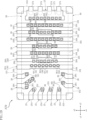
- FIG. FIG. 2 is a plan view showing the semiconductor device of FIG. 1, and is a view through a sealing resin.
- FIG. 3 is a plan view showing the semiconductor device of FIG. 1, and is a view through a semiconductor element.
- 4 is a bottom view showing the semiconductor device of FIG. 1.
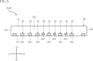
- FIG. 5 is a front view showing the semiconductor device of FIG. 1.
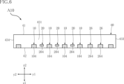
- FIG. 6 is a rear view showing the semiconductor device of FIG. 1.
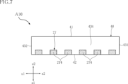
- FIG. 7 is a right side view of the semiconductor device of FIG. 1.
- FIG. 8 is a left side view of the semiconductor device of FIG. 1.
- FIG. 9 is a cross-sectional view taken along line IX-IX in FIG. 3.
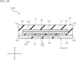
- FIG. 10 is a cross-sectional view taken along line XX of FIG. 3.
- FIG. 11 is a cross-sectional view along line XI-XI in FIG. 12 is a partially enlarged view of FIG. 9.
- FIG. 13 is a partially enlarged view of FIG. 9.
- FIG. 14 is a partially enlarged cross-sectional view showing a semiconductor device according to a second embodiment of the present disclosure;
- FIG. 15 is a partially enlarged cross-sectional view showing a semiconductor device according to a third embodiment of the present disclosure;
- FIG. 16 is a partially enlarged cross-sectional view showing a semiconductor device according to a fourth embodiment of the present disclosure;
- FIG. 17 is a partially enlarged cross-sectional view showing a semiconductor device according to a fifth embodiment of the present disclosure
- FIG. 18 is a partially enlarged cross-sectional view showing a semiconductor device according to a sixth embodiment of the present disclosure
- FIG. 19 is a plan view showing a semiconductor device according to a seventh embodiment of the present disclosure, and is a view through a sealing resin and a semiconductor element.
- FIG. 20 is a partially enlarged cross-sectional view showing a semiconductor device according to an eighth embodiment of the present disclosure.
- First embodiment: 1 to 13 show an example of a semiconductor device according to the present disclosure.
- the semiconductor device A10 of this embodiment includes a plurality of leads 10, a plurality of leads 20, a plurality of leads 25, a plurality of leads 26, a lead 27, a plurality of bonding materials 5, a plurality of metal layers 6, a semiconductor element 30, and a sealing.
- a stopper resin 40 is provided.
- the package format of the semiconductor device A10 is not particularly limited, and in this embodiment, as shown in FIG. 1, it is a QFN (Quad Flat Non-leaded package) type. Further, the usage and function of the semiconductor device A10 are not limited at all. For example, the semiconductor device A10 is used as one element forming a circuit of a DC/DC converter.
- FIG. 1 is a perspective view showing the semiconductor device A10.
- FIG. 2 is a plan view showing the semiconductor device A10.
- the outer shape of the sealing resin 40 is shown by an imaginary line (chain double-dashed line) through the sealing resin 40 .
- FIG. 3 is a plan view showing the semiconductor device A10.
- the encapsulating resin 40 and the semiconductor element 30 are shown through the encapsulating resin 40 and the semiconductor element 30 by imaginary lines (double-dot chain lines).
- FIG. 4 is a bottom view showing the semiconductor device A10.
- FIG. 5 is a front view showing the semiconductor device A10.
- FIG. 6 is a back view showing the semiconductor device A10.
- FIG. 7 is a right side view showing the semiconductor device A10.
- FIG. 5 is a front view showing the semiconductor device A10.
- FIG. 6 is a back view showing the semiconductor device A10.
- FIG. 7 is a right side view showing the semiconductor device A10.
- FIG. 8 is a left side view of the semiconductor device A10.
- 9 is a cross-sectional view taken along line IX-IX in FIG. 3.
- FIG. 10 is a cross-sectional view taken along line XX of FIG. 3.
- FIG. 11 is a cross-sectional view along line XI-XI in FIG. 12 is a partially enlarged view of FIG. 9.
- FIG. 13 is a partially enlarged view of FIG. 9.
- the semiconductor device A10 is plate-shaped, and has a long rectangular shape when viewed in the thickness direction (planar view).
- an example of the “thickness direction” (planar view direction) of the semiconductor device A10 is defined as the z-direction, and the direction along the short side of the semiconductor device A10 orthogonal to the z-direction (vertical direction in FIGS. 2 to 4).
- An example is the x-direction, the z-direction, and the y-direction is an example of a direction perpendicular to the x-direction (horizontal direction in FIGS. 2 to 4).
- One side in the z direction (the lower side in FIGS.
- the z direction corresponds to an example of the "thickness direction" of the present disclosure.
- the shape and dimensions of the semiconductor device A10 are not limited.
- the plurality of leads 10, the plurality of leads 20, the plurality of leads 25, the plurality of leads 26, and the leads 27 are arranged apart from each other.
- the plurality of leads 10, the plurality of leads 20, the plurality of leads 25, the plurality of leads 26, and the leads 27 support the semiconductor element 30 and mount the semiconductor device A10 on the wiring substrate, as shown in FIG. terminal.
- each of the plurality of leads 10, the plurality of leads 20, the plurality of leads 25, the plurality of leads 26, and the leads 27 is partially covered with a sealing resin 40. . 1, 4 to 8, a plurality of discrete points are formed on portions of the plurality of leads 10, the plurality of leads 20, the plurality of leads 25, the plurality of leads 26, and the leads 27 exposed from the sealing resin 40.
- the hatching consisting of Hereinafter, when the plurality of leads 10, the plurality of leads 20, the plurality of leads 25, the plurality of leads 26, and the leads 27 are collectively indicated, they may be described as "conductive member 1".
- the conductive member 1 is composed of, for example, a lead frame formed by etching a metal plate. Note that the method for forming the conductive member 1 is not limited.
- a constituent material of the conductive member 1 is, for example, Cu or a Cu alloy, but is not limited thereto.
- a plurality of (four in this embodiment) leads 10 each extend in the x direction, as shown in FIGS.
- a plurality of leads 10 are arranged at predetermined intervals in the y direction.
- Each of the plurality of leads 10 is an input terminal to which DC power (voltage) to be converted in the semiconductor device A10 is input.
- the lead 10 is a positive electrode (P terminal).
- the lead 10 has a main surface 101, two back surfaces 102, a concave surface 103, and two end surfaces 104.
- the main surface 101 and the back surface 102 face opposite sides in the z-direction.
- the main surface 101 faces the z-direction z2 side and faces the semiconductor element 30 .
- Main surface 101 is covered with sealing resin 40 .
- the semiconductor element 30 is supported on the main surface 101 .
- the back surface 102 faces the z-direction z1 side and is exposed from the sealing resin 40 .
- the two back surfaces 102 are arranged at both ends of the lead 10 in the x direction.
- a concave surface 103 is located between the two back surfaces 102 in the x-direction.
- the concave surface 103 is positioned on the principal surface 101 side (z2 side in the z direction) with respect to the back surface 102 in the z direction.
- the concave surface 103 is covered with the sealing resin 40 .
- the lead 10 has a width dimension (y-direction dimension) of a portion where the back surface 102 is located larger than a width dimension (y-direction dimension) of a portion where the concave surface 103 is located.
- End surface 104 is connected to both main surface 101 and back surface 102 .
- One end face 104 is positioned at the end of the lead 10 on the x1 side in the x direction and faces the x1 side.
- the other end face 104 is located at the end of the lead 10 on the x2 side in the x direction and faces the x2 side.
- Each end face 104 is exposed from the sealing resin 40 .
- the plurality of leads 10 includes leads 10A.
- the lead 10A is positioned closest to the x1 side in the x direction.
- the lead 10A has a body portion 11 and a projecting portion 12, as shown in FIG.
- the body portion 11 is a portion located on the back surface 102 side (z direction z1 side) from the main surface 101 .
- the protrusion 12 is a portion that protrudes from the main surface 101 in the z direction z2.
- the projecting portion 12 overlaps a joint surface 365 of the electrode terminal 36, which will be described later, when viewed in the z direction.
- a plurality of (three in this embodiment) leads 20 each extend in the x direction, as shown in FIGS.
- the plurality of leads 20 are arranged at predetermined intervals in the y direction.
- Each lead 20 is arranged between leads 10 adjacent in the y direction.
- the plurality of leads 10 and the plurality of leads 20 are alternately arranged in the y direction.
- Each of the plurality of leads 20 outputs AC power (voltage) that is power-converted by a switching circuit 321 (described later) formed in the semiconductor element 30 .
- the lead 20 has a main surface 201, a back surface 202, a concave surface 203, and two end surfaces 204.
- the main surface 201 and the back surface 202 face opposite sides in the z-direction.
- the main surface 201 faces the z-direction z2 side and faces the semiconductor element 30 .
- Main surface 201 is covered with sealing resin 40 .
- semiconductor element 30 is supported on main surface 201 .
- the back surface 202 faces the z-direction z1 side and is exposed from the sealing resin 40 .
- the back surface 202 is arranged in the center of the lead 20 in the x direction.
- the back surface 202 does not overlap any of the back surfaces 102 of the leads 10 when viewed in the y direction.
- the concave surface 203 surrounds the back surface 202 and extends to both ends of the lead 20 in the x direction.
- the concave surface 203 is positioned on the principal surface 201 side (z2 side in the z direction) with respect to the back surface 202 in the z direction.
- the concave surface 203 is covered with the sealing resin 40 .
- the width dimension (dimension in the y direction) of the portion of the lead 20 where the back surface 202 is located is larger than the width dimension (dimension in the y direction) of the portion where the back surface 202 is not located.
- End surface 204 is connected to both main surface 201 and concave surface 203 .
- One end surface 204 is located at the end of the lead 20 on the x1 side in the x direction and faces the x1 side.
- the other end face 204 is positioned at the end of the lead 20 on the x2 direction side and faces the x2 direction side.
- Each end surface 204 is exposed from the sealing resin 40 .
- the plurality of leads 20 includes leads 20A.
- the lead 20A is positioned closest to the y-direction y1 side among the plurality of leads 20, and is adjacent to the lead 10A and positioned on the y-direction y2 side of the lead 10A.
- the lead 20A has a body portion 21 and a projecting portion 22, as shown in FIG.
- the body portion 21 is a portion located on the back surface 202 side (z direction z1 side) from the main surface 201 .
- the protrusion 22 is a portion that protrudes from the main surface 201 in the z direction z2.
- the plurality of (four in this embodiment) leads 25 are located on the y-direction y1 side of the leads 10A, and are located at the end of the semiconductor device A10 on the y-direction y1 side.
- Power (voltage) for driving a control circuit 322, which will be described later, or an electric signal for transmission to the control circuit 322 is input to each of the leads 25, for example.
- lead 25 has major surface 251 , back surface 252 and end surface 254 .
- the main surface 251 and the back surface 252 face opposite sides in the z-direction.
- the main surface 251 faces the z-direction z2 side and faces the semiconductor element 30 .
- the main surface 251 is covered with the sealing resin 40 .
- semiconductor element 30 is supported on main surface 251 .
- the rear surface 252 faces the z-direction z1 side and is exposed from the sealing resin 40 .
- the rear surface 252 is arranged at the end of the lead 25 on the y1 side in the y direction.
- End surface 254 is connected to both main surface 251 and back surface 252 .
- the end face 254 is positioned at the end of the lead 25 on the y1 side in the y direction and faces the y1 side in the y direction.
- the end surface 254 is exposed from the sealing resin 40 .
- the end faces 254 of the multiple leads 25 are arranged at predetermined intervals along the x direction.
- a plurality of (four in this embodiment) leads 26 are positioned between the lead 10A and the plurality of leads 25 in the y direction, as shown in FIG. Some of the plurality of leads 26 (two in this embodiment) are positioned at the end of the semiconductor device A10 on the x-direction x1 side. Other leads 26 (two in this embodiment) are located at the end of the semiconductor device A10 on the x-direction x2 side. An electrical signal is input to each of the leads 26 for transmission to the control circuit 322, for example. As shown in FIGS. 3 and 4, lead 26 has major surface 261 , back surface 262 and end surface 264 . The main surface 261 and the back surface 262 face opposite sides in the z-direction.
- the main surface 261 faces the z-direction z2 side and faces the semiconductor element 30 .
- the main surface 261 is covered with the sealing resin 40 .
- semiconductor element 30 is supported on main surface 261 .
- the back surface 262 faces the z-direction z1 side and is exposed from the sealing resin 40 .
- the back surface 262 is located at the x-direction outer end of the lead 26 .
- End surface 264 is connected to both main surface 261 and back surface 262 .
- the end face 264 is positioned at the x-direction outer end of the lead 26 and faces outward in the x-direction.
- the end surface 264 is exposed from the sealing resin 40 .
- the end faces 264 are arranged along the y-direction along with the end faces 104 of the leads 10 and the end faces 204 of the leads 20 .
- the leads 27 are located on the y2 side in the y direction with respect to the plurality of leads 10, as shown in FIG.
- the lead 27 is an input terminal to which DC power (voltage) to be converted in the semiconductor device A10 is input.
- the lead 27 is a negative electrode (N terminal).
- the lead 27 has a major surface 271 , a plurality of back surfaces 272 , a concave surface 273 and a plurality of end surfaces 274 .
- the main surface 271 and the back surface 272 face opposite sides in the z-direction.
- the main surface 271 faces the z-direction z2 side and faces the semiconductor element 30 .
- the main surface 271 is covered with the sealing resin 40 .
- the semiconductor element 30 is supported on the main surface 271 of the leads 27 .
- the back surface 272 faces the z-direction z1 side and is exposed from the sealing resin 40 .
- the rear surface 272 is arranged at the end of the lead 27 on the y2 side in the y direction.
- a plurality of (four in this embodiment) rear surfaces 272 are spaced apart from each other in the x direction and arranged at predetermined intervals along the x direction.
- the concave surface 273 is positioned closer to the y1 side of the lead 27 in the y direction.
- the concave surface 273 is located on the main surface 271 side (z2 side in the z direction) with respect to the back surface 272 in the z direction.
- the concave surface 273 is covered with the sealing resin 40 .
- Each end surface 274 is connected to both the main surface 271 and one of the back surfaces 272 .
- the end face 274 is located at the end of the lead 27 on the y2 side in the y direction and faces the y2 side in the y direction.
- the end surface 264 is exposed from the sealing resin 40 .
- the plurality of end surfaces 274 are arranged at predetermined intervals along the x direction.
- Back surface 102 and end surface 104 of each lead 10, back surface 202 and end surface 204 of each lead 20, back surface 252 and end surface 254 of each lead 25, back surface 262 and end surface 264 of each lead 26, and back surface 272 and end surface 274 of lead 27. may be plated with Sn, for example.
- Sn plating a plurality of metal platings in which Ni, Pd, and Au are laminated in this order, for example, may be adopted.
- the number, shape, and arrangement of leads 10, 20, 25, 26, and 27 are not limited.
- the semiconductor element 30 is arranged in the center of the semiconductor device A10 when viewed in the z direction.
- the semiconductor element 30 is supported by a plurality of leads 10, a plurality of leads 20, a plurality of leads 25, a plurality of leads 26, and a lead 27, as shown in FIGS.
- the semiconductor element 30 is covered with a sealing resin 40 .
- the semiconductor element 30 has a semiconductor substrate 31 , a semiconductor layer 32 , a passivation film 33 , an electrode 34 , an insulating layer 35 and a plurality of electrode terminals 36 .
- the semiconductor element 30 is a flip-chip type LSI in which a circuit is configured.
- the semiconductor element 30 has a rectangular shape when viewed in the z direction as shown in FIG. 2, and a plate shape as shown in FIGS.
- the semiconductor element 30 has an element main surface 30a and an element rear surface 30b.
- the element main surface 30a includes the main surface 101 of the plurality of leads 10, the main surface 201 of the plurality of leads 20, the main surface 251 of the plurality of leads 25, the main surface 261 of the plurality of leads 26, and the main surface 261 of the plurality of leads 27 in the z direction. It faces the main surface 271 .
- the element rear surface 30b faces the side opposite to the element main surface 30a in the z direction.
- the semiconductor substrate 31 is provided with a semiconductor layer 32, a passivation film 33, an electrode 34, an insulating layer 35, and a plurality of electrode terminals 36 on the z-direction z1 side.
- the constituent material of the semiconductor substrate 31 is, for example, Si (silicon) or SiC (silicon carbide).
- the surface of the semiconductor substrate 31 on the z-direction z2 side constitutes the element back surface 30b.
- the semiconductor layer 32 is laminated on the semiconductor substrate 31 on the z-direction z1 side.
- the semiconductor layer 32 includes a plurality of types of p-type semiconductors and n-type semiconductors based on different amounts of doped elements.
- a switching circuit 321 and a control circuit 322 electrically connected to the switching circuit 321 are formed in the semiconductor layer 32 .
- the switching circuit 321 includes a plurality of switching elements such as MOSFETs (Metal-Oxide-Semiconductor Field-Effect Transistors) or IGBTs (Insulated Gate Bipolar Transistors).
- the switching circuit 321 is divided into two regions, a high voltage region (upper arm circuit) and a low voltage region (lower arm circuit). Each region comprises, for example, an n-channel MOSFET.
- the control circuit 322 includes a gate driver for driving the switching circuit 321, a bootstrap circuit corresponding to the high voltage region of the switching circuit 321, and the like, and performs control for normally driving the switching circuit 321. .
- a wiring layer (not shown) is further formed in the semiconductor layer 32 . The wiring layer electrically connects the switching circuit 321 and the control circuit 322 to each other.
- the passivation film 33 covers the surface of the semiconductor layer 32 on the z-direction z1 side.
- Passivation film 33 has electrical insulation.
- the passivation film 33 is composed of, for example, a silicon oxide film (SiO 2 ) laminated in contact with the semiconductor layer 32 and a silicon nitride film (Si 3 N 4 ) laminated on the silicon oxide film.
- the surface of the passivation film 33 on the z-direction z1 side constitutes the element main surface 30a.
- a plurality of electrodes 34 are formed on the element main surface 30a.
- the shape and arrangement of each electrode 34 when viewed in the z-direction are not limited.
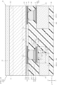
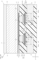
- Each electrode 34 is connected to a wiring layer formed in the semiconductor layer 32 through an opening (not shown) provided in the passivation film 33 . Thereby, each electrode 34 is electrically connected to either the switching circuit 321 or the control circuit 322 of the semiconductor layer 32 . Further, as shown in FIGS. 12 and 13, each electrode 34 is electrically connected to the conductive member 1 via an electrode terminal 36, respectively.
- the electrode 34 is composed of a plurality of metal layers laminated from the passivation film 33 toward the z-direction z1 side, and includes a first layer 34a, a second layer 34b, and a third layer 34c. ing.
- the first layer 34a is in contact with the passivation film 33 and is made of Cu.
- the second layer 34b is in contact with the first layer 34a and is made of Ni.
- the third layer 34c is in contact with the second layer 34b and is made of Pd. Note that the configuration of the electrode 34 is not limited.
- the insulating layer 35 is formed on the element main surface 30a and partially covers the passivation film 33 and the electrodes 34. As shown in FIGS.
- the insulating layer 35 has electrical insulation.
- the constituent material of the insulating layer 35 is phenol resin in this embodiment.
- the constituent material of the insulating layer 35 is not limited, and other insulating materials such as polyimide resin may be used.
- the insulating layer 35 has a plurality of openings 35a. One of the electrodes 34 is exposed from each of the plurality of openings 35a.
- the insulating layer 35 is formed, for example, by applying a photolithographic technique to a photosensitive resin material applied by a spin coater.
- the plurality of electrode terminals 36 are arranged on the element main surface 30a and protrude toward the conductive member 1. As shown in FIG. As shown in FIGS. 12 and 13, each electrode terminal 36 is in contact with one of the electrodes 34 through the opening 35a of the insulating layer 35, respectively. Each electrode terminal 36 is in contact with the electrode 34 at its central portion when viewed in the z-direction, and overlaps the insulating layer 35 at its peripheral portion.
- the multiple electrode terminals 36 are conductive.
- each electrode terminal 36 includes a seed layer 361, a first plating layer 362, and a second plating layer 363.
- the seed layer 361 is in contact with the electrode 34 and the insulating layer 35 and contains Cu.
- Seed layer 361 is formed, for example, by electroless plating.
- the constituent material and formation method of the seed layer 361 are not limited.
- seed layer 361 may be formed by a sputtering method.
- the first plated layer 362 is laminated on the seed layer 361 and is made of, for example, Cu or a Cu alloy.
- the first plating layer 362 is formed by electrolytic plating.
- the constituent material of the first plating layer 362 is not limited.
- the second plating layer 363 is laminated on the first plating layer 362 .
- the second plating layer 363 is interposed between the first plating layer 362 and the bonding material 5 and functions to suppress the chemical reaction between the first plating layer 362 and the bonding material 5 .
- the constituent material of the second plating layer 363 is not particularly limited, and a metal capable of suppressing a chemical reaction is appropriately selected, and examples thereof include Ni and Fe.
- the first plating layer 362 contains Cu and the bonding material 5 contains Sn, so the second plating layer 363 is made of Ni, for example.
- the second plating layer 363 is formed by electrolytic plating.
- the constituent material and formation method of the second plating layer 363 are not limited.
- Each electrode terminal 36 has a joint surface 365 .
- the joint surface 365 is a surface facing away from the electrode 34 (a surface facing the conductive member 1 ), and is joined to the metal layer 6 formed on the conductive member 1 via the joint material 5 .
- the electrode terminals 36 electrically connected to the plurality of leads 10 , the plurality of leads 20 , or the leads 27 of the conductive member 1 are electrically connected to the switching circuit 321 of the semiconductor layer 32 .
- the plurality of leads 10 , the plurality of leads 20 and the leads 27 are electrically connected to the switching circuit 321 .
- at least one electrode terminal 36 overlaps the rear surface 202 of each lead 20 when viewed in the z direction.
- three electrode terminals 36 overlap each other on the back surface 202 of each lead 20 when viewed in the z-direction.
- Electrode terminals 36 electrically connected to the plurality of leads 25 or 26 of the conductive member 1 are electrically connected to the control circuit 322 of the semiconductor layer 32 .
- the plurality of leads 25 and the plurality of leads 26 are electrically connected to the control circuit 322 .
- the shape of the electrode terminal 36 when viewed in the z-direction is circular, and the joint surface 365 of the electrode terminal 36 is also circular.
- the diameter of the joint surface 365 is not particularly limited, for example, it is 100 ⁇ m.
- the shape and dimensions of the electrode terminal 36 as viewed in the z direction are not limited.
- the shape of each electrode terminal 36 when viewed in the z-direction may be, for example, an elliptical shape, a rectangular shape, or a polygonal shape.
- the electrode terminals 36 may have different shapes or dimensions.
- one or more metal layers 6 are formed on the plurality of leads 10, the plurality of leads 20, the plurality of leads 25, the plurality of leads 26, and the leads 27, respectively.
- Each metal layer 6 is arranged according to the position of the electrode terminal 36 of the semiconductor element 30 .
- Electrode terminals 36 of the semiconductor element 30 are joined to each metal layer 6 .
- the shape of each metal layer 6 when viewed in the z-direction is circular, matching the shape of the joint surface 365 of the electrode terminal 36 .
- the diameter of the metal layer 6 is larger than the diameter of the joint surface 365 .
- the electrode terminal 36 (joint surface 365 ) is included in the metal layer 6 when viewed in the z direction. As shown in FIGS.
- each metal layer 6 is interposed between the conductive member 1 and the electrode terminal 36 , and the electrode terminal 36 is joined by the joining material 5 .
- the metal layer 6 suppresses a chemical reaction between the conductive member 1 and the bonding material 5 and regulates the range over which the bonding material 5 spreads when the semiconductor element 30 is bonded.
- the multiple metal layers 6 include multiple metal layers 6A and multiple metal layers 6B.
- a plurality of metal layers 6A are formed on leads 10A and leads 20A.
- a plurality of metal layers 6B are formed on the conductive member 1 other than the leads 10A.
- a metal layer 6A and a metal layer 6B are formed on the lead 20A.
- Each metal layer 6B is included in one of the main surfaces 101, 201, 251, 261, 271 when viewed in the z direction.
- Each metal layer 6B also has a first metal layer 601, as shown in FIG.
- the first metal layer 601 has a first layer 61 , a second layer 62 and a third layer 63 .
- the first layer 61 is laminated in contact with any one of the main surfaces 101 , 201 , 251 , 261 and 271 .
- the conductive member 1 contains Cu and the bonding material 5 contains Sn, so the first layer 61 is made of Ni, for example.
- the second layer 62 is laminated in contact with the first layer 61 .
- the constituent material of the second layer 62 is not particularly limited, and includes Pd, for example.
- the third layer 63 is laminated in contact with the second layer 62 .
- the third layer 63 is made of a constituent material having relatively good wettability with the bonding material 5 (solder).
- a constituent material of the third layer 63 is not particularly limited, and includes Au, for example.
- the number of layers of the first metal layer 601 is not limited, and the constituent material of each layer is not limited.
- the thickness (z-direction dimension) of the first metal layer 601 is not particularly limited, but is about 5 to 10 ⁇ m.
- Each metal layer 6A is formed on a lead 10A or a lead 20A, as shown in FIG. Each metal layer 6A is not included in the lead 10A or the lead 20A when viewed in the z-direction.
- each metal layer 6A formed on the lead 10A protrudes from the lead 10A in the y direction y2.
- each metal layer 6A formed on the lead 20A protrudes from the lead 20A in the y direction y1. That is, each metal layer 6A formed on the lead 10A and each metal layer 6A formed on the lead 20A are arranged so as to be close to each other in the y direction.
- Each metal layer 6A has a metal layer suspending portion 6Aa which is suspended without overlapping the leads 10A (20A) when viewed in the z direction.
- the metal layer suspended portion 6Aa does not overlap the main body portion 11 of the lead 10A (the main body portion 21 of the lead 20A).
- each metal layer 6A is formed on the top surface of the projecting portion 12 of the lead 10 (the surface facing the z-direction z2 side) or the top surface of the projecting portion 22 of the lead 20 (the surface facing the z-direction z2 side). surface) and is spaced apart from each of the main surfaces 101 and 201 .
- Each metal layer 6A comprises a first metal layer 601 and a second metal layer 602, as shown in FIG.
- the first metal layer 601 has the same configuration as the first metal layer 601 of the metal layer 6A, and the first layer 61 is laminated in contact with the second metal layer 602 .
- the second metal layer 602 is laminated in contact with the top surfaces of the protrusions 12 and 22 .
- the second metal layer 602 encloses the first metal layer 601 when viewed in the z-direction.
- the configuration of the second metal layer 602 is not limited.
- the second metal layer 602 may have a first layer 61 , a second layer 62 and a third layer 63 in a configuration similar to that of the first metal layer 601 .
- the thickness (z-direction dimension) of the second metal layer 602 is not particularly limited, but is about 1 to 10 ⁇ m.
- the second metal layer 602 of the metal layer 6A is formed at a predetermined position of the lead frame lead 10A and lead 20A. Thereafter, for example, an etching process is performed to form main body portion 11 and protruding portion 12 of lead 10A and main body portion 21 and protruding portion 22 of lead 20A. The second metal layer 602 is partially supported by the protruding portions 12 and 22 and protrudes from the body portions 11 and 21 . After that, a first metal layer 601 is laminated on each predetermined position of the lead frame. The first metal layer 601 laminated on the second metal layer 602 becomes the metal layer 6A together with the second metal layer 602 . The first metal layer 601 directly laminated on the lead frame becomes the metal layer 6B. Note that the method of forming the metal layers 6A and 6B is not limited.
- the electrode terminals 36 joined to each metal layer 6A are not included in the leads 10A or 20A when viewed in the z direction.
- the electrode terminal 36A electrically connected to the lead 10A protrudes from the lead 10A in the y direction y2.
- the electrode terminal 36A electrically connected to the lead 20A protrudes from the lead 20A to the y-direction y1 side. That is, the electrode terminal 36A electrically connected to the lead 10A and the electrode terminal 36A electrically connected to the lead 20A are arranged so as to approach each other in the y direction.
- a joint surface 365 of each electrode terminal 36A has a suspended portion 365a that does not overlap the lead 10A (20A) when viewed in the z direction.
- the suspended portion 365a does not overlap the main body portion 11 of the lead 10A (the main body portion 21 of the lead 20A).
- the area of the suspended portion 365a is not particularly limited, it is desirable to be about 10% or more and 50% or less of the area of the joint surface 365.
- the suspended portion 365a of the electrode terminal 36A electrically connected to the lead 10A and the suspended portion 365a of the electrode terminal 36A electrically connected to the lead 20A are positioned between the lead 10A and the lead 20A.
- the electrode terminal 36A conducting to the lead 10A and the electrode terminal 36A conducting to the lead 20A are joined to different electrodes 34 separated from each other.
- a switching element is formed between the electrode 34 electrically connected to the lead 10A and the electrode 34 electrically connected to the lead 20A when viewed in the z direction.
- a first terminal (drain terminal) of the switching element is conductively connected to the lead 10A via the wiring layer, the electrode 34, and the electrode terminal 36A, and a second terminal (source terminal) is connected to the wiring layer, the electrode 34, and the electrode terminal 36A. It is conductively connected to the lead 20A via the electrode terminal 36A. The shorter the distance between the electrode 34 conducting to the lead 10A and the electrode 34 conducting to the lead 20A, the shorter the current path in the wiring layer electrically connected to the switching element.
- the bonding material 5 has conductivity, is interposed between the electrode terminal 36 and the metal layer 6, and conducts them to each other.
- the bonding material 5 is made of, for example, solder containing Sn (SnAg, etc.).
- the constituent material of the bonding material 5 is not limited.
- the constituent material of the bonding material 5 may be, for example, Ag paste or other conductive material such as sintered metal (sintered Ag).
- the shape of the bonding material 5 is a truncated cone shape in which the upper surface is in contact with the bonding surface 365 and the lower surface is in contact with the metal layer 6 . Note that the shape of the bonding material 5 is not limited.
- the bonding material 5 is formed in advance by electrolytic plating so as to be in contact with the bonding surface 365 of each electrode terminal 36 of the semiconductor element 30 .
- the semiconductor element 30 is bonded to the conductive member 1 by flip-chip bonding. Specifically, the semiconductor element 30 is brought close to the conductive member 1 with the element main surface 30a facing the conductive member 1 in a state where the bonding material 5 is melted by reflow. Each melted bonding material 5 contacts the first metal layer 601 of the corresponding metal layer 6 .
- the third layer 63 of the first metal layer 601 has relatively good solder wettability.
- the bonding material 5 spreads over the entire surface of the first metal layer 601 so as not to protrude from the first metal layer 601 when viewed in the z direction.
- the bonding material 5 has a truncated cone shape in which the cross-sectional area perpendicular to the z-direction increases from the electrode terminal 36 toward the metal layer 6 in the z-direction. Then, by cooling, the bonding material 5 is solidified and the electrode terminal 36 and the metal layer 6 are bonded.
- the sealing resin 40 covers the entire semiconductor element 30 and part of each of the plurality of leads 10 , the plurality of leads 20 , the plurality of leads 25 , the plurality of leads 26 and the leads 27 .
- Sealing resin 40 is made of a material containing, for example, black epoxy resin. Note that the material of the sealing resin 40 is not limited.
- the sealing resin 40 has a rectangular shape when viewed in the z direction, and has a top surface 41, a bottom surface 42, a first side surface 431, a second side surface 432, a third side surface 433 and a fourth side surface 434, as shown in FIGS. have
- the top surface 41 faces the same side as the main surface 101 of the lead 10 in the z direction. Also, the bottom surface 42 faces the opposite side of the top surface 41 . 4 and 9 to 11, from the bottom surface 42, each rear surface 102 of the plurality of leads 10, the rear surface 202 of the plurality of leads 20, the rear surface 252 of the plurality of leads 25, the rear surface 262 of the plurality of leads 26, and the back surface 272 of each lead 27 is exposed.
- the first side surface 431 is connected to both the top surface 41 and the bottom surface 42 and faces the x direction x2.
- the second side surface 432 is connected to both the top surface 41 and the bottom surface 42 and faces the x1 side in the x direction.
- the first side surface 431 and the second side surface 432 are separated from each other in the x-direction. 5, 6, 10, and 11, from the first side surface 431, the end faces 104 of the plurality of leads 10, the end faces 204 of the plurality of leads 20, and some of the leads 26 is exposed so as to be flush with the first side surface 431 .
- the end surfaces 104 of the plurality of leads 10 , the end surfaces 204 of the plurality of leads 20 , and the end surface 264 of some of the plurality of leads 26 are flush with the second side surface 432 . exposed like this.
- the third side surface 433 is connected to all of the top surface 41, the bottom surface 42, the first side surface 431, and the second side surface 432, and faces the y direction y1 side.
- the fourth side surface 434 is connected to all of the top surface 41, the bottom surface 42, the first side surface 431, and the second side surface 432, and faces the y direction y2.
- the third side 433 and the fourth side 434 are separated from each other in the y direction. 7 to 9, end surfaces 254 of the plurality of leads 25 are exposed from the third side surface 433 so as to be flush with the third side surface 433.
- a plurality of end surfaces 274 of the lead 27 are exposed from the fourth side surface 434 so as to be flush with the fourth side surface 434 .
- the electrode terminal 36A electrically connected to the lead 10A protrudes from the lead 10A in the y direction y2. Further, the electrode terminal 36A electrically connected to the lead 20A protrudes from the lead 20A to the y-direction y1 side. That is, as shown in FIG. 13, the electrode terminal 36A electrically connected to the lead 10A and the electrode terminal 36A electrically connected to the lead 20A are arranged so as to approach each other in the y direction. Therefore, compared to the case where the electrode terminal 36 does not protrude from the leads 10A and 20A (see FIG. 12), the distance between the electrode 34 electrically connected to the lead 10A and the electrode 34 electrically connected to the lead 20A is reduced. The current path can be shortened. Thereby, the semiconductor device A10 can suppress the electrical resistance in the current path.
- the semiconductor device A10 includes a plurality of leads 10 extending in the x direction.
- a plurality of leads 10 are arranged at intervals in the y direction.
- Each lead 10 has a main surface 101 on which the semiconductor element 30 is mounted, and two back surfaces 102 and a concave surface 103 facing opposite to the main surface 101 in the z-direction.
- the two back surfaces 102 are separated from each other across the concave surface 103 in the x direction and are exposed from the bottom surface 42 of the sealing resin 40 .
- the concave surface 103 is covered with the sealing resin 40 . That is, in the semiconductor device A10, the rear surfaces 102 of the leads 10 are distributed in both the x direction and the y direction.
- the semiconductor device A10 can disperse and release the heat generated in the semiconductor element 30, so that the heat can be uniformly dissipated.
- each rear surface 102 serves as a joint portion when mounted on a wiring board, the semiconductor device A10 has many joint portions, and mounting reliability is enhanced.
- the semiconductor device A10 includes a plurality of leads 20 extending in the x direction.
- a plurality of leads 20 are arranged between leads 10 adjacent to each other in the y direction.
- Each lead 20 has a main surface 201 on which the semiconductor element 30 is mounted, and a back surface 202 and a concave surface 203 facing away from the main surface 201 in the z-direction.
- the back surface 202 is located in the center of the lead 20 in the x direction and exposed from the bottom surface 42 of the sealing resin 40 .
- the concave surface 203 is covered with the sealing resin 40 . Therefore, the rear surfaces 102 of adjacent leads 10 are prevented from approaching each other. In addition, the rear surfaces 102 and 202 of adjacent leads 10 and 20 are prevented from approaching each other.
- the rear surface 202 does not overlap any of the rear surfaces 102 of the leads 10 when viewed in the y direction. Therefore, adjacent leads 10 and 20 are more reliably prevented from having their rear surfaces 102 and 202 approach each other.
- the lead 10 has a width dimension of the portion where the back surface 102 is located larger than the width dimension of the portion where the concave surface 103 is located. Therefore, it is possible to reduce the arrangement pitch of the leads 10 adjacent to each other with the lead 20 interposed therebetween in the y direction. This is preferable for miniaturization of the semiconductor device A10.
- the semiconductor element 30 is mounted on the conductive member 1 by so-called flip-chip bonding. Therefore, the semiconductor device A10 can suppress the resistance of the current path and can be made low-profile compared to a semiconductor device in which each electrode 34 and each lead are electrically connected by wires. Furthermore, when the sealing resin 40 has the same external size in plan view, the semiconductor device A10 can mount a larger semiconductor element 30 than a semiconductor device that conducts with wires. Moreover, when the same semiconductor element 30 is mounted, the semiconductor device A10 can have a smaller outer shape of the sealing resin 40 than a semiconductor device that conducts with wires.
- each metal layer 6A is formed on the lead 10A or the lead 20A, that is, the case where each electrode terminal 36A is joined to the lead 10A or the lead 20A has been described, but the present invention is not limited to this. do not have.
- the lead on which the metal layer 6A is formed that is, the lead to which the electrode terminal 36A is joined is not limited.
- the electrode terminals 36 to be joined to different leads are to be arranged close to each other on the element main surface 30a of the semiconductor element 30, these electrode terminals 36 are used as the electrode terminals 36A, and the leads to which the electrode terminals 36A are joined are formed.
- the metal layer 6 to be coated may be the metal layer 6A.
- the semiconductor element 30 is an LSI has been described, but the present invention is not limited to this.
- the type of semiconductor element 30 is not limited.
- the number, shape, and arrangement of the leads that constitute the conductive member 1 provided in the semiconductor device A10 are not limited.
- FIG. 14 is a diagram for explaining the semiconductor device A20 according to the second embodiment of the present disclosure.
- FIG. 14 is a partially enlarged cross-sectional view showing the semiconductor device A20, corresponding to FIG.
- the semiconductor device A20 of this embodiment differs from the first embodiment in that the metal layer 6A does not include the second metal layer 602.
- FIG. The configuration and operation of other portions of this embodiment are the same as those of the first embodiment.
- the metal layer 6A does not include the second metal layer 602, but includes only the first metal layer 601. That is, in this embodiment, the metal layer 6A has the same structure as the metal layer 6B, and the first layer 61 of the first metal layer 601 is in contact with the top surfaces of the protruding portions 12 and 22 .
- the electrode terminals 36A electrically connected to the leads 10A and the electrode terminals 36A electrically connected to the leads 20A protrude from the leads 10A and 20A, respectively, and are arranged so as to approach each other in the y direction.
- the distance between the electrode 34 electrically connected to the lead 10A and the electrode 34 electrically connected to the lead 20A can be reduced, so that the semiconductor device A20 can shorten the current path in the wiring layer and suppress the electrical resistance in the current path.
- the semiconductor device A20 has the same effect as the semiconductor device A10 due to the configuration common to the semiconductor device A10.
- FIG. 15 is a diagram for explaining a semiconductor device A30 according to the third embodiment of the present disclosure.
- FIG. 15 is a partially enlarged cross-sectional view showing the semiconductor device A30, corresponding to FIG.
- the semiconductor device A30 of this embodiment differs from the first embodiment in that the lead 10A does not have the projecting portion 12 and the lead 20A does not have the projecting portion 22.
- FIG. The configuration and operation of other portions of this embodiment are the same as those of the first embodiment. Note that each part of the above first and second embodiments may be combined arbitrarily.
- the lead 10A does not have the projecting portion 12, and the metal layer 6A is arranged in contact with the main surface 101.
- the lead 20A does not have the projecting portion 12, and the metal layer 6A is arranged in contact with the main surface 201. As shown in FIG.
- the electrode terminals 36A electrically connected to the leads 10A and the electrode terminals 36A electrically connected to the leads 20A protrude from the leads 10A and 20A, respectively, and are arranged so as to approach each other in the y direction.
- the distance between the electrode 34 electrically connected to the lead 10A and the electrode 34 electrically connected to the lead 20A can be reduced, so that the semiconductor device A30 can shorten the current path in the wiring layer and suppress the electrical resistance in the current path.
- the semiconductor device A30 has the same effect as the semiconductor device A10 due to the configuration common to the semiconductor device A10.
- FIG. 16 is a diagram for explaining a semiconductor device A40 according to the fourth embodiment of the present disclosure.
- FIG. 16 is a partially enlarged cross-sectional view showing the semiconductor device A40, corresponding to FIG.
- the semiconductor device A40 of this embodiment differs from the first embodiment in that the lead 10A further includes a receiving plate portion 13 and the lead 20A further includes a receiving plate portion 23.
- FIG. The configuration and operation of other portions of this embodiment are the same as those of the first embodiment. Note that each part of the above first to third embodiments may be combined arbitrarily.
- the lead 10A further includes a receiving plate portion 13.
- the receiving plate portion 13 is interposed between the projecting portion 12 and the metal layer 6 ⁇ /b>A and is connected to the projecting portion 12 .
- the lead 20A further includes a saucer portion 23.
- the receiving plate portion 23 is interposed between the projecting portion 22 and the metal layer 6A and is connected to the projecting portion 22 .
- the shape and dimensions of the saucer portions 13 and 23 are not limited. 6 A of metal layers are formed in contact with the surface which faces the z direction z2 side of the saucer parts 13 and 23. As shown in FIG.
- the saucer portions 13 and 23 are portions that were in contact with the metal layer 6A and could not be completely removed when the projecting portions 12 (22) of the leads 10A (20A) were formed by etching. In this embodiment, it cannot be said that the electrode terminal 36A protrudes from the leads 10 and 20 when viewed in the z direction. However, the electrode terminal 36A protrudes from the body portions 11 and 21 when viewed in the z direction.
- the suspended portion 365a is a portion of the joint surface 365 that does not overlap the main body portion 11 of the lead 10A (the main body portion 21 of the lead 20A).
- the electrode terminal 36A electrically connected to the lead 10A protrudes from the main body portion 11 of the lead 10A in the y direction y2. Further, the electrode terminal 36A electrically connected to the lead 20A protrudes from the body portion 11 of the lead 20A in the y direction y1. That is, the electrode terminal 36A electrically connected to the lead 10A and the electrode terminal 36A electrically connected to the lead 20A are arranged so as to approach each other in the y direction. As a result, the distance between the electrode 34 electrically connected to the lead 10A and the electrode 34 electrically connected to the lead 20A can be reduced, so that the semiconductor device A40 can shorten the current path in the wiring layer and suppress the electrical resistance in the current path. In addition, the semiconductor device A40 has the same effect as the semiconductor device A10 due to the configuration common to the semiconductor device A10.
- FIG. 17 is a diagram for explaining a semiconductor device A50 according to the fifth embodiment of the present disclosure.
- FIG. 17 is a partially enlarged cross-sectional view showing the semiconductor device A50, corresponding to FIG.
- the semiconductor device A50 of this embodiment differs from the first embodiment in that the electrode terminals 36 electrically connected to the leads 20A do not protrude from the leads 20A.
- the configuration and operation of other portions of this embodiment are the same as those of the first embodiment. It should be noted that each part of the above-described first to fourth embodiments may be combined arbitrarily.
- the electrode terminal 36 electrically connected to the lead 20A is not the electrode terminal 36A, and the metal layer 6 formed on the lead 20A is not the metal layer 6A but the metal layer 6B. That is, the lead 20A is the same as the other leads 20, and the electrode terminal 36 electrically connected to the lead 20A does not protrude from the lead 20A.
- the electrode terminal 36A electrically connected to the lead 10A protrudes from the lead 10A in the y direction y2. That is, the electrode terminal 36A electrically connected to the lead 10A is arranged so as to be close to the electrode terminal 36 electrically connected to the lead 20A. Therefore, the distance between the electrode 34 electrically connected to the lead 10A and the electrode 34 electrically connected to the lead 20A is smaller than when the electrode terminal 36 does not protrude from either of the leads 10A and 20A (see FIG. 12). A current path in the wiring layer can be shortened. Thereby, the semiconductor device A50 can suppress the electrical resistance in the current path. Further, the semiconductor device A50 has the same effect as the semiconductor device A10 due to the configuration common to the semiconductor device A10.
- FIG. 18 is a diagram for explaining a semiconductor device A60 according to the sixth embodiment of the present disclosure.
- FIG. 18 is a partially enlarged cross-sectional view showing the semiconductor device A60, corresponding to FIG.
- the semiconductor device A60 of this embodiment differs from the first embodiment in that the metal layer 6A does not protrude from the lead 10A or the lead 20A when viewed in the z direction.
- the configuration and operation of other portions of this embodiment are the same as those of the first embodiment. It should be noted that each part of the above-described first to fifth embodiments may be combined arbitrarily.
- the metal layer 6A does not include the second metal layer 602, but includes only the first metal layer 601. That is, in this embodiment, the metal layer 6A has the same configuration as the metal layer 6B. Moreover, the lead 10A (20A) does not have the projecting portion 12 (22), and the metal layer 6A is formed in contact with the main surface 101 (201). The metal layer 6A is included in the leads 10A and 20A without protruding from the leads 10A and 20A when viewed in the z direction. On the other hand, as in the first embodiment, the electrode terminal 36A electrically connected to the lead 10A protrudes from the lead 10A in the y direction y2.
- the electrode terminal 36A electrically connected to the lead 20A protrudes from the lead 20A to the y-direction y1 side. That is, the electrode terminal 36A electrically connected to the lead 10A and the electrode terminal 36A electrically connected to the lead 20A are arranged so as to approach each other in the y direction. Each electrode terminal 36A is joined to the corresponding metal layer 6A via the joining material 5. As shown in FIG.
- the electrode terminals 36A electrically connected to the leads 10A and the electrode terminals 36A electrically connected to the leads 20A protrude from the leads 10A and 20A, respectively, and are arranged so as to approach each other in the y direction.
- the distance between the electrode 34 electrically connected to the lead 10A and the electrode 34 electrically connected to the lead 20A can be reduced, so that the semiconductor device A60 can shorten the current path in the wiring layer and suppress the electrical resistance in the current path.
- the semiconductor device A60 has the same effect as the semiconductor device A10 due to the configuration common to the semiconductor device A10.
- the electrode terminal 36A may be directly bonded to the principal surface 101 of the lead 10A via the bonding material 5 without forming the metal layer 6A on the lead 10A.
- the metal layer 6A may not be formed on the lead 20A, and the electrode terminal 36A may be directly joined to the main surface 201 of the lead 20A via the joining material 5.
- FIG. 19 is a diagram for explaining a semiconductor device A70 according to the seventh embodiment of the present disclosure.
- FIG. 19 is a plan view showing the semiconductor device A70, corresponding to FIG. In FIG. 19 , for convenience of understanding, the encapsulating resin 40 and the semiconductor element 30 are shown through the encapsulating resin 40 and the semiconductor element 30 by imaginary lines (two-dot chain lines).
- the semiconductor device A70 of this embodiment differs from that of the first embodiment in the shape of the electrode terminal 36 and the metal layer 6 .
- the configuration and operation of other portions of this embodiment are the same as those of the first embodiment. Note that each part of the above first to sixth embodiments may be combined arbitrarily.
- each electrode terminal 36 as viewed in the z-direction is rectangular. Therefore, the joint surface 365 of each electrode terminal 36 also has the same rectangular shape.
- the shape of each metal layer 6 as viewed in the z-direction is rectangular to match the shape of the joint surface 365 of the electrode terminal 36 .
- the electrode terminals 36A electrically connected to the leads 10A and the electrode terminals 36A electrically connected to the leads 20A protrude from the leads 10A and 20A, respectively, and are arranged so as to approach each other in the y direction.
- the distance between the electrode 34 conducting to the lead 10A and the electrode 34 conducting to the lead 20A can be reduced, so that the semiconductor device A70 can shorten the current path in the wiring layer and suppress the electrical resistance in the current path.
- the semiconductor device A70 has the same effect as the semiconductor device A10 due to the configuration common to the semiconductor device A10.
- the z-direction shape (planar shape) and each dimension of the electrode terminal 36 are not limited.
- the shape of each electrode terminal 36 when viewed in the z-direction may be, for example, an elliptical shape, a rectangular shape, or a polygonal shape.
- the electrode terminals 36 may have different shapes or dimensions.
- FIG. 20 is a diagram for explaining a semiconductor device A80 according to the eighth embodiment of the present disclosure.
- FIG. 20 is a partially enlarged cross-sectional view showing the semiconductor device A80, corresponding to FIG.
- the semiconductor device A80 of the present embodiment differs from the first embodiment in that the electrode terminal 36 electrically connected to the lead 10A and the electrode terminal 36 electrically connected to the lead 20A are electrically connected to the same electrode 34.
- FIG. The configuration and operation of other portions of this embodiment are the same as those of the first embodiment. Note that each part of the above first to seventh embodiments may be combined arbitrarily.
- the semiconductor device A80 differs from the semiconductor device A10 in the internal configuration of the semiconductor element 30 and the shape and arrangement of the conductive member 1.
- the leads 10A and 20A are electrically connected through the electrodes 34 of the semiconductor element 30.
- FIG. The electrode terminal 36 electrically connected to the lead 10A and the electrode terminal 36 electrically connected to the lead 20A are in contact with and electrically connected to the same electrode 34, respectively.
- the electrode terminals 36A electrically connected to the leads 10A and the electrode terminals 36A electrically connected to the leads 20A protrude from the leads 10A and 20A, respectively, and are arranged so as to approach each other in the y direction.
- the distance between the position of the electrode 34 at which the electrode terminal 36 conducting to the lead 10A contacts and the position at which the electrode terminal 36 conducting to the lead 20A contacts can be reduced. It can be shortened, and electric resistance in the current path can be suppressed.
- the semiconductor device A80 has the same effect as the semiconductor device A10 due to the configuration common to the semiconductor device A10.
- the semiconductor device according to the present disclosure is not limited to the above-described embodiments.
- the specific configuration of each part of the semiconductor device according to the present disclosure can be changed in various ways.
- the present disclosure includes embodiments described in the appendices below.
- Appendix 1 An element main surface (30a) and an element back surface (30b) facing opposite to each other in the thickness direction, an electrode layer formed on the element main surface, and being in contact with the electrode layer and protruding in the thickness direction a semiconductor element (30) having electrode terminals (36A); a first lead (10A) electrically connected to the semiconductor element and having a first main surface (101) and a first rear surface (102) facing opposite sides in the thickness direction; a sealing resin (40) covering the semiconductor element; with The first lead has a first body portion (11) located closer to the first rear surface than the first principal surface, The electrode terminal has a joint surface (365) facing the first lead, The semiconductor device according to claim 1, wherein the bonding surface has a suspended portion (365a) that does not overlap the first body portion when viewed in the thickness direction.
- Appendix 2 The semiconductor device according to appendix 1, wherein the suspended portion does not overlap the first lead when viewed in the thickness direction. Appendix 3. 3. The semiconductor device according to appendix 1 or 2, wherein the area of the suspended portion is 10% or more and 50% or less of the area of the bonding surface. Appendix 4. 4. The semiconductor device according to any one of appendices 1 to 3, further comprising a metal layer (6A) formed on the first lead and to which the electrode terminal is joined. Appendix 5. 5. The semiconductor device according to appendix 4, wherein the metal layer includes a metal layer suspending portion (6Aa) that does not overlap the first body portion when viewed in the thickness direction. Appendix 6.
- said metal layer comprises a first metal layer (601) and a second metal layer (602); the second metal layer is in contact with the first lead; 6.
- the semiconductor device according to appendix 4 or 5 wherein the first metal layer is in contact with the second metal layer and is included in the second metal layer when viewed in the thickness direction.
- Appendix 7. The semiconductor device according to any one of Appendixes 4 to 6, wherein the shape of the metal layer when viewed in the thickness direction and the shape of the bonding surface are circular. Supplementary Note 8, Third Embodiment, FIG. 8. The semiconductor device according to any one of Appendixes 4 to 7, wherein the metal layer is arranged in contact with the first main surface. Appendix 9.
- the first lead has a projecting portion (12) projecting from the first main surface in the thickness direction and overlapping the bonding surface when viewed in the thickness direction; 8.
- Appendix 10. further comprising a bonding material (5) interposed between the bonding surface and the first lead; 10.
- a second lead (20A) which is spaced apart from the first lead and conducts to the semiconductor element and has a second main surface (201) and a second rear surface (202) facing opposite to each other in the thickness direction; further prepared, the second lead has a second body portion (21) located closer to the second rear surface than the second main surface;
- the semiconductor element has a second electrode terminal (36A) that is in contact with the electrode layer and protrudes in the thickness direction,
- the second electrode terminal has a second joint surface (365) facing the second lead, 11.
- the semiconductor device according to any one of appendices 1 to 10, wherein the second bonding surface includes a second suspended portion (365A) that does not overlap the second body portion when viewed in the thickness direction. Appendix 12. 12.
- said electrode layer comprising a first electrode (34) and a second electrode (34) spaced apart from each other; the electrode terminal is in contact with the first electrode; the second electrode terminal is in contact with the second electrode; 13.
- the semiconductor element comprises a switching element having a first terminal, a second terminal, and a control terminal, the first electrode is electrically connected to the first terminal of the switching element; 14.
- the electrode layer comprises a first electrode (34); 13.
- the semiconductor device according to appendix 11 or 12 wherein the electrode terminal and the second electrode terminal are in contact with the first electrode.
Landscapes
- Engineering & Computer Science (AREA)
- Physics & Mathematics (AREA)
- Condensed Matter Physics & Semiconductors (AREA)
- General Physics & Mathematics (AREA)
- Computer Hardware Design (AREA)
- Microelectronics & Electronic Packaging (AREA)
- Power Engineering (AREA)
- Manufacturing & Machinery (AREA)
- Lead Frames For Integrated Circuits (AREA)
Abstract
L'invention concerne un dispositif à semi-conducteurs A10 comprenant : un élément semi-conducteur 30 ayant une surface principale d'élément 30a et une surface arrière d'élément 30b faisant face à des côtés opposés l'un à l'autre dans une direction z, des électrodes 34 formées sur la surface principale de l'élément 30a, et des bornes d'électrode 36a qui sont en contact avec les électrodes 34 et qui font saillie dans la direction z ; un conducteur 10A qui a une surface principale 101 et une surface arrière 102 faisant face à des côtés opposés l'un à l'autre dans la direction z et qui établit une connexion électrique avec l'élément semi-conducteur 30 ; et une résine d'étanchéité 40 qui recouvre l'élément semi-conducteur 30. Le conducteur 10A comprend une partie de corps 11 située plus près de la surface arrière 102 que de la surface principale 101. Les bornes d'électrode 36A comportent chacune une surface de jonction 365 faisant face au conducteur 10. La surface de jonction 365 a une partie de suspension 365a qui ne chevauche pas la partie corps 11 lorsqu'elle est vue dans la direction z.
Applications Claiming Priority (2)
| Application Number | Priority Date | Filing Date | Title |
|---|---|---|---|
| JP2021190267 | 2021-11-24 | ||
| JP2021-190267 | 2021-11-24 |
Publications (1)
| Publication Number | Publication Date |
|---|---|
| WO2023095681A1 true WO2023095681A1 (fr) | 2023-06-01 |
Family
ID=86539660
Family Applications (1)
| Application Number | Title | Priority Date | Filing Date |
|---|---|---|---|
| PCT/JP2022/042404 WO2023095681A1 (fr) | 2021-11-24 | 2022-11-15 | Dispositif à semi-conducteurs |
Country Status (1)
| Country | Link |
|---|---|
| WO (1) | WO2023095681A1 (fr) |
Citations (5)
| Publication number | Priority date | Publication date | Assignee | Title |
|---|---|---|---|---|
| JP2000156389A (ja) * | 1998-11-20 | 2000-06-06 | Fujitsu Ltd | テープキャリアパッケージ |
| WO2001069678A1 (fr) * | 2000-03-13 | 2001-09-20 | Dai Nippon Printing Co., Ltd. | Dispositif semi-conducteur sous enveloppe de resine, element de circuit destine a ce dispositif et procede de fabrication de cet element de circuit |
| JP2010258200A (ja) * | 2009-04-24 | 2010-11-11 | Panasonic Corp | 半導体装置およびその製造方法 |
| JP2020077723A (ja) * | 2018-11-07 | 2020-05-21 | ローム株式会社 | 半導体装置 |
| JP2020155483A (ja) * | 2019-03-18 | 2020-09-24 | ローム株式会社 | 半導体装置および半導体パッケージ |
-
2022
- 2022-11-15 WO PCT/JP2022/042404 patent/WO2023095681A1/fr unknown
Patent Citations (5)
| Publication number | Priority date | Publication date | Assignee | Title |
|---|---|---|---|---|
| JP2000156389A (ja) * | 1998-11-20 | 2000-06-06 | Fujitsu Ltd | テープキャリアパッケージ |
| WO2001069678A1 (fr) * | 2000-03-13 | 2001-09-20 | Dai Nippon Printing Co., Ltd. | Dispositif semi-conducteur sous enveloppe de resine, element de circuit destine a ce dispositif et procede de fabrication de cet element de circuit |
| JP2010258200A (ja) * | 2009-04-24 | 2010-11-11 | Panasonic Corp | 半導体装置およびその製造方法 |
| JP2020077723A (ja) * | 2018-11-07 | 2020-05-21 | ローム株式会社 | 半導体装置 |
| JP2020155483A (ja) * | 2019-03-18 | 2020-09-24 | ローム株式会社 | 半導体装置および半導体パッケージ |
Similar Documents
| Publication | Publication Date | Title |
|---|---|---|
| JP6509885B2 (ja) | 半導体チップの端子を有するdc−dcコンバータ | |
| JP7199921B2 (ja) | 半導体装置 | |
| JP2005064479A (ja) | 回路モジュール | |
| US20240038612A1 (en) | Package with electrically insulated carrier and at least one step on encapsulant | |
| US10290567B2 (en) | Transistor package with three-terminal clip | |
| US10879155B2 (en) | Electronic device with double-sided cooling | |
| US20130256920A1 (en) | Semiconductor device | |
| WO2022080081A1 (fr) | Dispositif à semi-conducteur | |
| WO2023095681A1 (fr) | Dispositif à semi-conducteurs | |
| US20220301966A1 (en) | Semiconductor device | |
| WO2022059251A1 (fr) | Dispositif à semi-conducteur | |
| JP7473376B2 (ja) | 半導体装置 | |
| JP7339000B2 (ja) | 半導体装置および半導体パッケージ | |
| WO2023136078A1 (fr) | Dispositif à semi-conducteur | |
| US9362221B2 (en) | Surface mountable power components | |
| WO2021251128A1 (fr) | Élément à semi-conducteur et dispositif à semi-conducteur | |
| KR20190085587A (ko) | 고열전도성 반도체 패키지 | |
| US20230245951A1 (en) | Semiconductor device | |
| WO2023100663A1 (fr) | Dispositif à semi-conducteurs | |
| JP2023082291A (ja) | 半導体素子、半導体装置、および、半導体素子の製造方法 | |
| US20220301967A1 (en) | Semiconductor device | |
| WO2023017707A1 (fr) | Dispositif à semi-conducteurs | |
| WO2023203934A1 (fr) | Dispositif à semi-conducteur et procédé de fabrication de dispositif à semi-conducteur | |
| WO2022270305A1 (fr) | Dispositif à semi-conducteur et procédé de fabrication de dispositif à semi-conducteur | |
| WO2023136074A1 (fr) | Dispositif à semi-conducteur |
Legal Events
| Date | Code | Title | Description |
|---|---|---|---|
| 121 | Ep: the epo has been informed by wipo that ep was designated in this application |
Ref document number: 22898465 Country of ref document: EP Kind code of ref document: A1 |