WO2023095681A1 - Semiconductor device - Google Patents
Semiconductor device Download PDFInfo
- Publication number
- WO2023095681A1 WO2023095681A1 PCT/JP2022/042404 JP2022042404W WO2023095681A1 WO 2023095681 A1 WO2023095681 A1 WO 2023095681A1 JP 2022042404 W JP2022042404 W JP 2022042404W WO 2023095681 A1 WO2023095681 A1 WO 2023095681A1
- Authority
- WO
- WIPO (PCT)
- Prior art keywords
- lead
- semiconductor device
- electrode
- metal layer
- leads
- Prior art date
Links
Images


Classifications
-
- H—ELECTRICITY
- H01—ELECTRIC ELEMENTS
- H01L—SEMICONDUCTOR DEVICES NOT COVERED BY CLASS H10
- H01L21/00—Processes or apparatus adapted for the manufacture or treatment of semiconductor or solid state devices or of parts thereof
- H01L21/02—Manufacture or treatment of semiconductor devices or of parts thereof
- H01L21/04—Manufacture or treatment of semiconductor devices or of parts thereof the devices having at least one potential-jump barrier or surface barrier, e.g. PN junction, depletion layer or carrier concentration layer
- H01L21/50—Assembly of semiconductor devices using processes or apparatus not provided for in a single one of the subgroups H01L21/06 - H01L21/326, e.g. sealing of a cap to a base of a container
- H01L21/60—Attaching or detaching leads or other conductive members, to be used for carrying current to or from the device in operation
-
- H—ELECTRICITY
- H01—ELECTRIC ELEMENTS
- H01L—SEMICONDUCTOR DEVICES NOT COVERED BY CLASS H10
- H01L23/00—Details of semiconductor or other solid state devices
- H01L23/48—Arrangements for conducting electric current to or from the solid state body in operation, e.g. leads, terminal arrangements ; Selection of materials therefor
- H01L23/50—Arrangements for conducting electric current to or from the solid state body in operation, e.g. leads, terminal arrangements ; Selection of materials therefor for integrated circuit devices, e.g. power bus, number of leads
Definitions
- the present disclosure relates to semiconductor devices.
- a semiconductor device has been proposed in which a plurality of leads and a semiconductor element are bonded in the form of a so-called flip chip.
- a semiconductor device is disclosed in Patent Document 1, for example.
- the semiconductor device includes multiple leads, a semiconductor element, a bonding layer, and a sealing resin.
- the semiconductor element is mounted on the leads with the plurality of first electrodes facing the leads.
- Each first electrode has a base electrically connected to the semiconductor layer and a columnar portion projecting from the base toward the lead. The columnar portion is joined to the lead via the joining layer.
- a plurality of leads are arranged with a predetermined interval or more from each other.
- a first electrode joined to a certain lead and a first electrode joined to another lead are separated from each other according to the distance between the leads. As the distance between the first electrodes increases, the electric resistance in the current path increases because the current path formed inside the semiconductor layer increases.
- An object of the present disclosure is to provide an improved semiconductor device.
- an object of the present disclosure is to provide a semiconductor device capable of suppressing electrical resistance in a current path.
- a semiconductor device provided according to one aspect of the present disclosure includes an element main surface and an element back surface facing opposite sides in a thickness direction, an electrode layer formed on the element main surface, in contact with the electrode layer, and and electrode terminals projecting in the thickness direction; and a first lead electrically connected to the semiconductor element and having a first main surface and a first back surface facing opposite to each other in the thickness direction. and a sealing resin that covers the semiconductor element.
- the first lead further has a first main body positioned closer to the first rear surface than the first main surface.
- the electrode terminal has a bonding surface facing the first lead.
- the joint surface has a suspended portion that does not overlap the first body portion when viewed in the thickness direction.
- FIG. 1 is a perspective view showing a semiconductor device according to a first embodiment of the present disclosure
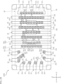
- FIG. FIG. 2 is a plan view showing the semiconductor device of FIG. 1, and is a view through a sealing resin.
- FIG. 3 is a plan view showing the semiconductor device of FIG. 1, and is a view through a semiconductor element.
- 4 is a bottom view showing the semiconductor device of FIG. 1.
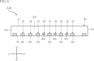
- FIG. 5 is a front view showing the semiconductor device of FIG. 1.
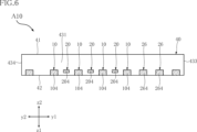
- FIG. 6 is a rear view showing the semiconductor device of FIG. 1.
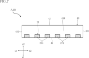
- FIG. 7 is a right side view of the semiconductor device of FIG. 1.
- FIG. 8 is a left side view of the semiconductor device of FIG. 1.
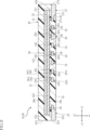
- FIG. 9 is a cross-sectional view taken along line IX-IX in FIG. 3.
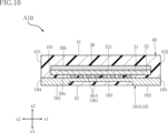
- FIG. 10 is a cross-sectional view taken along line XX of FIG. 3.
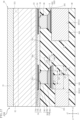
- FIG. 11 is a cross-sectional view along line XI-XI in FIG. 12 is a partially enlarged view of FIG. 9.
- FIG. 13 is a partially enlarged view of FIG. 9.
- FIG. 14 is a partially enlarged cross-sectional view showing a semiconductor device according to a second embodiment of the present disclosure;
- FIG. 15 is a partially enlarged cross-sectional view showing a semiconductor device according to a third embodiment of the present disclosure;
- FIG. 16 is a partially enlarged cross-sectional view showing a semiconductor device according to a fourth embodiment of the present disclosure;
- FIG. 17 is a partially enlarged cross-sectional view showing a semiconductor device according to a fifth embodiment of the present disclosure
- FIG. 18 is a partially enlarged cross-sectional view showing a semiconductor device according to a sixth embodiment of the present disclosure
- FIG. 19 is a plan view showing a semiconductor device according to a seventh embodiment of the present disclosure, and is a view through a sealing resin and a semiconductor element.
- FIG. 20 is a partially enlarged cross-sectional view showing a semiconductor device according to an eighth embodiment of the present disclosure.
- First embodiment: 1 to 13 show an example of a semiconductor device according to the present disclosure.
- the semiconductor device A10 of this embodiment includes a plurality of leads 10, a plurality of leads 20, a plurality of leads 25, a plurality of leads 26, a lead 27, a plurality of bonding materials 5, a plurality of metal layers 6, a semiconductor element 30, and a sealing.
- a stopper resin 40 is provided.
- the package format of the semiconductor device A10 is not particularly limited, and in this embodiment, as shown in FIG. 1, it is a QFN (Quad Flat Non-leaded package) type. Further, the usage and function of the semiconductor device A10 are not limited at all. For example, the semiconductor device A10 is used as one element forming a circuit of a DC/DC converter.
- FIG. 1 is a perspective view showing the semiconductor device A10.
- FIG. 2 is a plan view showing the semiconductor device A10.
- the outer shape of the sealing resin 40 is shown by an imaginary line (chain double-dashed line) through the sealing resin 40 .
- FIG. 3 is a plan view showing the semiconductor device A10.
- the encapsulating resin 40 and the semiconductor element 30 are shown through the encapsulating resin 40 and the semiconductor element 30 by imaginary lines (double-dot chain lines).
- FIG. 4 is a bottom view showing the semiconductor device A10.
- FIG. 5 is a front view showing the semiconductor device A10.
- FIG. 6 is a back view showing the semiconductor device A10.
- FIG. 7 is a right side view showing the semiconductor device A10.
- FIG. 5 is a front view showing the semiconductor device A10.
- FIG. 6 is a back view showing the semiconductor device A10.
- FIG. 7 is a right side view showing the semiconductor device A10.
- FIG. 8 is a left side view of the semiconductor device A10.
- 9 is a cross-sectional view taken along line IX-IX in FIG. 3.
- FIG. 10 is a cross-sectional view taken along line XX of FIG. 3.
- FIG. 11 is a cross-sectional view along line XI-XI in FIG. 12 is a partially enlarged view of FIG. 9.
- FIG. 13 is a partially enlarged view of FIG. 9.
- the semiconductor device A10 is plate-shaped, and has a long rectangular shape when viewed in the thickness direction (planar view).
- an example of the “thickness direction” (planar view direction) of the semiconductor device A10 is defined as the z-direction, and the direction along the short side of the semiconductor device A10 orthogonal to the z-direction (vertical direction in FIGS. 2 to 4).
- An example is the x-direction, the z-direction, and the y-direction is an example of a direction perpendicular to the x-direction (horizontal direction in FIGS. 2 to 4).
- One side in the z direction (the lower side in FIGS.
- the z direction corresponds to an example of the "thickness direction" of the present disclosure.
- the shape and dimensions of the semiconductor device A10 are not limited.
- the plurality of leads 10, the plurality of leads 20, the plurality of leads 25, the plurality of leads 26, and the leads 27 are arranged apart from each other.
- the plurality of leads 10, the plurality of leads 20, the plurality of leads 25, the plurality of leads 26, and the leads 27 support the semiconductor element 30 and mount the semiconductor device A10 on the wiring substrate, as shown in FIG. terminal.
- each of the plurality of leads 10, the plurality of leads 20, the plurality of leads 25, the plurality of leads 26, and the leads 27 is partially covered with a sealing resin 40. . 1, 4 to 8, a plurality of discrete points are formed on portions of the plurality of leads 10, the plurality of leads 20, the plurality of leads 25, the plurality of leads 26, and the leads 27 exposed from the sealing resin 40.
- the hatching consisting of Hereinafter, when the plurality of leads 10, the plurality of leads 20, the plurality of leads 25, the plurality of leads 26, and the leads 27 are collectively indicated, they may be described as "conductive member 1".
- the conductive member 1 is composed of, for example, a lead frame formed by etching a metal plate. Note that the method for forming the conductive member 1 is not limited.
- a constituent material of the conductive member 1 is, for example, Cu or a Cu alloy, but is not limited thereto.
- a plurality of (four in this embodiment) leads 10 each extend in the x direction, as shown in FIGS.
- a plurality of leads 10 are arranged at predetermined intervals in the y direction.
- Each of the plurality of leads 10 is an input terminal to which DC power (voltage) to be converted in the semiconductor device A10 is input.
- the lead 10 is a positive electrode (P terminal).
- the lead 10 has a main surface 101, two back surfaces 102, a concave surface 103, and two end surfaces 104.
- the main surface 101 and the back surface 102 face opposite sides in the z-direction.
- the main surface 101 faces the z-direction z2 side and faces the semiconductor element 30 .
- Main surface 101 is covered with sealing resin 40 .
- the semiconductor element 30 is supported on the main surface 101 .
- the back surface 102 faces the z-direction z1 side and is exposed from the sealing resin 40 .
- the two back surfaces 102 are arranged at both ends of the lead 10 in the x direction.
- a concave surface 103 is located between the two back surfaces 102 in the x-direction.
- the concave surface 103 is positioned on the principal surface 101 side (z2 side in the z direction) with respect to the back surface 102 in the z direction.
- the concave surface 103 is covered with the sealing resin 40 .
- the lead 10 has a width dimension (y-direction dimension) of a portion where the back surface 102 is located larger than a width dimension (y-direction dimension) of a portion where the concave surface 103 is located.
- End surface 104 is connected to both main surface 101 and back surface 102 .
- One end face 104 is positioned at the end of the lead 10 on the x1 side in the x direction and faces the x1 side.
- the other end face 104 is located at the end of the lead 10 on the x2 side in the x direction and faces the x2 side.
- Each end face 104 is exposed from the sealing resin 40 .
- the plurality of leads 10 includes leads 10A.
- the lead 10A is positioned closest to the x1 side in the x direction.
- the lead 10A has a body portion 11 and a projecting portion 12, as shown in FIG.
- the body portion 11 is a portion located on the back surface 102 side (z direction z1 side) from the main surface 101 .
- the protrusion 12 is a portion that protrudes from the main surface 101 in the z direction z2.
- the projecting portion 12 overlaps a joint surface 365 of the electrode terminal 36, which will be described later, when viewed in the z direction.
- a plurality of (three in this embodiment) leads 20 each extend in the x direction, as shown in FIGS.
- the plurality of leads 20 are arranged at predetermined intervals in the y direction.
- Each lead 20 is arranged between leads 10 adjacent in the y direction.
- the plurality of leads 10 and the plurality of leads 20 are alternately arranged in the y direction.
- Each of the plurality of leads 20 outputs AC power (voltage) that is power-converted by a switching circuit 321 (described later) formed in the semiconductor element 30 .
- the lead 20 has a main surface 201, a back surface 202, a concave surface 203, and two end surfaces 204.
- the main surface 201 and the back surface 202 face opposite sides in the z-direction.
- the main surface 201 faces the z-direction z2 side and faces the semiconductor element 30 .
- Main surface 201 is covered with sealing resin 40 .
- semiconductor element 30 is supported on main surface 201 .
- the back surface 202 faces the z-direction z1 side and is exposed from the sealing resin 40 .
- the back surface 202 is arranged in the center of the lead 20 in the x direction.
- the back surface 202 does not overlap any of the back surfaces 102 of the leads 10 when viewed in the y direction.
- the concave surface 203 surrounds the back surface 202 and extends to both ends of the lead 20 in the x direction.
- the concave surface 203 is positioned on the principal surface 201 side (z2 side in the z direction) with respect to the back surface 202 in the z direction.
- the concave surface 203 is covered with the sealing resin 40 .
- the width dimension (dimension in the y direction) of the portion of the lead 20 where the back surface 202 is located is larger than the width dimension (dimension in the y direction) of the portion where the back surface 202 is not located.
- End surface 204 is connected to both main surface 201 and concave surface 203 .
- One end surface 204 is located at the end of the lead 20 on the x1 side in the x direction and faces the x1 side.
- the other end face 204 is positioned at the end of the lead 20 on the x2 direction side and faces the x2 direction side.
- Each end surface 204 is exposed from the sealing resin 40 .
- the plurality of leads 20 includes leads 20A.
- the lead 20A is positioned closest to the y-direction y1 side among the plurality of leads 20, and is adjacent to the lead 10A and positioned on the y-direction y2 side of the lead 10A.
- the lead 20A has a body portion 21 and a projecting portion 22, as shown in FIG.
- the body portion 21 is a portion located on the back surface 202 side (z direction z1 side) from the main surface 201 .
- the protrusion 22 is a portion that protrudes from the main surface 201 in the z direction z2.
- the plurality of (four in this embodiment) leads 25 are located on the y-direction y1 side of the leads 10A, and are located at the end of the semiconductor device A10 on the y-direction y1 side.
- Power (voltage) for driving a control circuit 322, which will be described later, or an electric signal for transmission to the control circuit 322 is input to each of the leads 25, for example.
- lead 25 has major surface 251 , back surface 252 and end surface 254 .
- the main surface 251 and the back surface 252 face opposite sides in the z-direction.
- the main surface 251 faces the z-direction z2 side and faces the semiconductor element 30 .
- the main surface 251 is covered with the sealing resin 40 .
- semiconductor element 30 is supported on main surface 251 .
- the rear surface 252 faces the z-direction z1 side and is exposed from the sealing resin 40 .
- the rear surface 252 is arranged at the end of the lead 25 on the y1 side in the y direction.
- End surface 254 is connected to both main surface 251 and back surface 252 .
- the end face 254 is positioned at the end of the lead 25 on the y1 side in the y direction and faces the y1 side in the y direction.
- the end surface 254 is exposed from the sealing resin 40 .
- the end faces 254 of the multiple leads 25 are arranged at predetermined intervals along the x direction.
- a plurality of (four in this embodiment) leads 26 are positioned between the lead 10A and the plurality of leads 25 in the y direction, as shown in FIG. Some of the plurality of leads 26 (two in this embodiment) are positioned at the end of the semiconductor device A10 on the x-direction x1 side. Other leads 26 (two in this embodiment) are located at the end of the semiconductor device A10 on the x-direction x2 side. An electrical signal is input to each of the leads 26 for transmission to the control circuit 322, for example. As shown in FIGS. 3 and 4, lead 26 has major surface 261 , back surface 262 and end surface 264 . The main surface 261 and the back surface 262 face opposite sides in the z-direction.
- the main surface 261 faces the z-direction z2 side and faces the semiconductor element 30 .
- the main surface 261 is covered with the sealing resin 40 .
- semiconductor element 30 is supported on main surface 261 .
- the back surface 262 faces the z-direction z1 side and is exposed from the sealing resin 40 .
- the back surface 262 is located at the x-direction outer end of the lead 26 .
- End surface 264 is connected to both main surface 261 and back surface 262 .
- the end face 264 is positioned at the x-direction outer end of the lead 26 and faces outward in the x-direction.
- the end surface 264 is exposed from the sealing resin 40 .
- the end faces 264 are arranged along the y-direction along with the end faces 104 of the leads 10 and the end faces 204 of the leads 20 .
- the leads 27 are located on the y2 side in the y direction with respect to the plurality of leads 10, as shown in FIG.
- the lead 27 is an input terminal to which DC power (voltage) to be converted in the semiconductor device A10 is input.
- the lead 27 is a negative electrode (N terminal).
- the lead 27 has a major surface 271 , a plurality of back surfaces 272 , a concave surface 273 and a plurality of end surfaces 274 .
- the main surface 271 and the back surface 272 face opposite sides in the z-direction.
- the main surface 271 faces the z-direction z2 side and faces the semiconductor element 30 .
- the main surface 271 is covered with the sealing resin 40 .
- the semiconductor element 30 is supported on the main surface 271 of the leads 27 .
- the back surface 272 faces the z-direction z1 side and is exposed from the sealing resin 40 .
- the rear surface 272 is arranged at the end of the lead 27 on the y2 side in the y direction.
- a plurality of (four in this embodiment) rear surfaces 272 are spaced apart from each other in the x direction and arranged at predetermined intervals along the x direction.
- the concave surface 273 is positioned closer to the y1 side of the lead 27 in the y direction.
- the concave surface 273 is located on the main surface 271 side (z2 side in the z direction) with respect to the back surface 272 in the z direction.
- the concave surface 273 is covered with the sealing resin 40 .
- Each end surface 274 is connected to both the main surface 271 and one of the back surfaces 272 .
- the end face 274 is located at the end of the lead 27 on the y2 side in the y direction and faces the y2 side in the y direction.
- the end surface 264 is exposed from the sealing resin 40 .
- the plurality of end surfaces 274 are arranged at predetermined intervals along the x direction.
- Back surface 102 and end surface 104 of each lead 10, back surface 202 and end surface 204 of each lead 20, back surface 252 and end surface 254 of each lead 25, back surface 262 and end surface 264 of each lead 26, and back surface 272 and end surface 274 of lead 27. may be plated with Sn, for example.
- Sn plating a plurality of metal platings in which Ni, Pd, and Au are laminated in this order, for example, may be adopted.
- the number, shape, and arrangement of leads 10, 20, 25, 26, and 27 are not limited.
- the semiconductor element 30 is arranged in the center of the semiconductor device A10 when viewed in the z direction.
- the semiconductor element 30 is supported by a plurality of leads 10, a plurality of leads 20, a plurality of leads 25, a plurality of leads 26, and a lead 27, as shown in FIGS.
- the semiconductor element 30 is covered with a sealing resin 40 .
- the semiconductor element 30 has a semiconductor substrate 31 , a semiconductor layer 32 , a passivation film 33 , an electrode 34 , an insulating layer 35 and a plurality of electrode terminals 36 .
- the semiconductor element 30 is a flip-chip type LSI in which a circuit is configured.
- the semiconductor element 30 has a rectangular shape when viewed in the z direction as shown in FIG. 2, and a plate shape as shown in FIGS.
- the semiconductor element 30 has an element main surface 30a and an element rear surface 30b.
- the element main surface 30a includes the main surface 101 of the plurality of leads 10, the main surface 201 of the plurality of leads 20, the main surface 251 of the plurality of leads 25, the main surface 261 of the plurality of leads 26, and the main surface 261 of the plurality of leads 27 in the z direction. It faces the main surface 271 .
- the element rear surface 30b faces the side opposite to the element main surface 30a in the z direction.
- the semiconductor substrate 31 is provided with a semiconductor layer 32, a passivation film 33, an electrode 34, an insulating layer 35, and a plurality of electrode terminals 36 on the z-direction z1 side.
- the constituent material of the semiconductor substrate 31 is, for example, Si (silicon) or SiC (silicon carbide).
- the surface of the semiconductor substrate 31 on the z-direction z2 side constitutes the element back surface 30b.
- the semiconductor layer 32 is laminated on the semiconductor substrate 31 on the z-direction z1 side.
- the semiconductor layer 32 includes a plurality of types of p-type semiconductors and n-type semiconductors based on different amounts of doped elements.
- a switching circuit 321 and a control circuit 322 electrically connected to the switching circuit 321 are formed in the semiconductor layer 32 .
- the switching circuit 321 includes a plurality of switching elements such as MOSFETs (Metal-Oxide-Semiconductor Field-Effect Transistors) or IGBTs (Insulated Gate Bipolar Transistors).
- the switching circuit 321 is divided into two regions, a high voltage region (upper arm circuit) and a low voltage region (lower arm circuit). Each region comprises, for example, an n-channel MOSFET.
- the control circuit 322 includes a gate driver for driving the switching circuit 321, a bootstrap circuit corresponding to the high voltage region of the switching circuit 321, and the like, and performs control for normally driving the switching circuit 321. .
- a wiring layer (not shown) is further formed in the semiconductor layer 32 . The wiring layer electrically connects the switching circuit 321 and the control circuit 322 to each other.
- the passivation film 33 covers the surface of the semiconductor layer 32 on the z-direction z1 side.
- Passivation film 33 has electrical insulation.
- the passivation film 33 is composed of, for example, a silicon oxide film (SiO 2 ) laminated in contact with the semiconductor layer 32 and a silicon nitride film (Si 3 N 4 ) laminated on the silicon oxide film.
- the surface of the passivation film 33 on the z-direction z1 side constitutes the element main surface 30a.
- a plurality of electrodes 34 are formed on the element main surface 30a.
- the shape and arrangement of each electrode 34 when viewed in the z-direction are not limited.
- Each electrode 34 is connected to a wiring layer formed in the semiconductor layer 32 through an opening (not shown) provided in the passivation film 33 . Thereby, each electrode 34 is electrically connected to either the switching circuit 321 or the control circuit 322 of the semiconductor layer 32 . Further, as shown in FIGS. 12 and 13, each electrode 34 is electrically connected to the conductive member 1 via an electrode terminal 36, respectively.
- the electrode 34 is composed of a plurality of metal layers laminated from the passivation film 33 toward the z-direction z1 side, and includes a first layer 34a, a second layer 34b, and a third layer 34c. ing.
- the first layer 34a is in contact with the passivation film 33 and is made of Cu.
- the second layer 34b is in contact with the first layer 34a and is made of Ni.
- the third layer 34c is in contact with the second layer 34b and is made of Pd. Note that the configuration of the electrode 34 is not limited.
- the insulating layer 35 is formed on the element main surface 30a and partially covers the passivation film 33 and the electrodes 34. As shown in FIGS.
- the insulating layer 35 has electrical insulation.
- the constituent material of the insulating layer 35 is phenol resin in this embodiment.
- the constituent material of the insulating layer 35 is not limited, and other insulating materials such as polyimide resin may be used.
- the insulating layer 35 has a plurality of openings 35a. One of the electrodes 34 is exposed from each of the plurality of openings 35a.
- the insulating layer 35 is formed, for example, by applying a photolithographic technique to a photosensitive resin material applied by a spin coater.
- the plurality of electrode terminals 36 are arranged on the element main surface 30a and protrude toward the conductive member 1. As shown in FIG. As shown in FIGS. 12 and 13, each electrode terminal 36 is in contact with one of the electrodes 34 through the opening 35a of the insulating layer 35, respectively. Each electrode terminal 36 is in contact with the electrode 34 at its central portion when viewed in the z-direction, and overlaps the insulating layer 35 at its peripheral portion.
- the multiple electrode terminals 36 are conductive.
- each electrode terminal 36 includes a seed layer 361, a first plating layer 362, and a second plating layer 363.
- the seed layer 361 is in contact with the electrode 34 and the insulating layer 35 and contains Cu.
- Seed layer 361 is formed, for example, by electroless plating.
- the constituent material and formation method of the seed layer 361 are not limited.
- seed layer 361 may be formed by a sputtering method.
- the first plated layer 362 is laminated on the seed layer 361 and is made of, for example, Cu or a Cu alloy.
- the first plating layer 362 is formed by electrolytic plating.
- the constituent material of the first plating layer 362 is not limited.
- the second plating layer 363 is laminated on the first plating layer 362 .
- the second plating layer 363 is interposed between the first plating layer 362 and the bonding material 5 and functions to suppress the chemical reaction between the first plating layer 362 and the bonding material 5 .
- the constituent material of the second plating layer 363 is not particularly limited, and a metal capable of suppressing a chemical reaction is appropriately selected, and examples thereof include Ni and Fe.
- the first plating layer 362 contains Cu and the bonding material 5 contains Sn, so the second plating layer 363 is made of Ni, for example.
- the second plating layer 363 is formed by electrolytic plating.
- the constituent material and formation method of the second plating layer 363 are not limited.
- Each electrode terminal 36 has a joint surface 365 .
- the joint surface 365 is a surface facing away from the electrode 34 (a surface facing the conductive member 1 ), and is joined to the metal layer 6 formed on the conductive member 1 via the joint material 5 .
- the electrode terminals 36 electrically connected to the plurality of leads 10 , the plurality of leads 20 , or the leads 27 of the conductive member 1 are electrically connected to the switching circuit 321 of the semiconductor layer 32 .
- the plurality of leads 10 , the plurality of leads 20 and the leads 27 are electrically connected to the switching circuit 321 .
- at least one electrode terminal 36 overlaps the rear surface 202 of each lead 20 when viewed in the z direction.
- three electrode terminals 36 overlap each other on the back surface 202 of each lead 20 when viewed in the z-direction.
- Electrode terminals 36 electrically connected to the plurality of leads 25 or 26 of the conductive member 1 are electrically connected to the control circuit 322 of the semiconductor layer 32 .
- the plurality of leads 25 and the plurality of leads 26 are electrically connected to the control circuit 322 .
- the shape of the electrode terminal 36 when viewed in the z-direction is circular, and the joint surface 365 of the electrode terminal 36 is also circular.
- the diameter of the joint surface 365 is not particularly limited, for example, it is 100 ⁇ m.
- the shape and dimensions of the electrode terminal 36 as viewed in the z direction are not limited.
- the shape of each electrode terminal 36 when viewed in the z-direction may be, for example, an elliptical shape, a rectangular shape, or a polygonal shape.
- the electrode terminals 36 may have different shapes or dimensions.
- one or more metal layers 6 are formed on the plurality of leads 10, the plurality of leads 20, the plurality of leads 25, the plurality of leads 26, and the leads 27, respectively.
- Each metal layer 6 is arranged according to the position of the electrode terminal 36 of the semiconductor element 30 .
- Electrode terminals 36 of the semiconductor element 30 are joined to each metal layer 6 .
- the shape of each metal layer 6 when viewed in the z-direction is circular, matching the shape of the joint surface 365 of the electrode terminal 36 .
- the diameter of the metal layer 6 is larger than the diameter of the joint surface 365 .
- the electrode terminal 36 (joint surface 365 ) is included in the metal layer 6 when viewed in the z direction. As shown in FIGS.
- each metal layer 6 is interposed between the conductive member 1 and the electrode terminal 36 , and the electrode terminal 36 is joined by the joining material 5 .
- the metal layer 6 suppresses a chemical reaction between the conductive member 1 and the bonding material 5 and regulates the range over which the bonding material 5 spreads when the semiconductor element 30 is bonded.
- the multiple metal layers 6 include multiple metal layers 6A and multiple metal layers 6B.
- a plurality of metal layers 6A are formed on leads 10A and leads 20A.
- a plurality of metal layers 6B are formed on the conductive member 1 other than the leads 10A.
- a metal layer 6A and a metal layer 6B are formed on the lead 20A.
- Each metal layer 6B is included in one of the main surfaces 101, 201, 251, 261, 271 when viewed in the z direction.
- Each metal layer 6B also has a first metal layer 601, as shown in FIG.
- the first metal layer 601 has a first layer 61 , a second layer 62 and a third layer 63 .
- the first layer 61 is laminated in contact with any one of the main surfaces 101 , 201 , 251 , 261 and 271 .
- the conductive member 1 contains Cu and the bonding material 5 contains Sn, so the first layer 61 is made of Ni, for example.
- the second layer 62 is laminated in contact with the first layer 61 .
- the constituent material of the second layer 62 is not particularly limited, and includes Pd, for example.
- the third layer 63 is laminated in contact with the second layer 62 .
- the third layer 63 is made of a constituent material having relatively good wettability with the bonding material 5 (solder).
- a constituent material of the third layer 63 is not particularly limited, and includes Au, for example.
- the number of layers of the first metal layer 601 is not limited, and the constituent material of each layer is not limited.
- the thickness (z-direction dimension) of the first metal layer 601 is not particularly limited, but is about 5 to 10 ⁇ m.
- Each metal layer 6A is formed on a lead 10A or a lead 20A, as shown in FIG. Each metal layer 6A is not included in the lead 10A or the lead 20A when viewed in the z-direction.
- each metal layer 6A formed on the lead 10A protrudes from the lead 10A in the y direction y2.
- each metal layer 6A formed on the lead 20A protrudes from the lead 20A in the y direction y1. That is, each metal layer 6A formed on the lead 10A and each metal layer 6A formed on the lead 20A are arranged so as to be close to each other in the y direction.
- Each metal layer 6A has a metal layer suspending portion 6Aa which is suspended without overlapping the leads 10A (20A) when viewed in the z direction.
- the metal layer suspended portion 6Aa does not overlap the main body portion 11 of the lead 10A (the main body portion 21 of the lead 20A).
- each metal layer 6A is formed on the top surface of the projecting portion 12 of the lead 10 (the surface facing the z-direction z2 side) or the top surface of the projecting portion 22 of the lead 20 (the surface facing the z-direction z2 side). surface) and is spaced apart from each of the main surfaces 101 and 201 .
- Each metal layer 6A comprises a first metal layer 601 and a second metal layer 602, as shown in FIG.
- the first metal layer 601 has the same configuration as the first metal layer 601 of the metal layer 6A, and the first layer 61 is laminated in contact with the second metal layer 602 .
- the second metal layer 602 is laminated in contact with the top surfaces of the protrusions 12 and 22 .
- the second metal layer 602 encloses the first metal layer 601 when viewed in the z-direction.
- the configuration of the second metal layer 602 is not limited.
- the second metal layer 602 may have a first layer 61 , a second layer 62 and a third layer 63 in a configuration similar to that of the first metal layer 601 .
- the thickness (z-direction dimension) of the second metal layer 602 is not particularly limited, but is about 1 to 10 ⁇ m.
- the second metal layer 602 of the metal layer 6A is formed at a predetermined position of the lead frame lead 10A and lead 20A. Thereafter, for example, an etching process is performed to form main body portion 11 and protruding portion 12 of lead 10A and main body portion 21 and protruding portion 22 of lead 20A. The second metal layer 602 is partially supported by the protruding portions 12 and 22 and protrudes from the body portions 11 and 21 . After that, a first metal layer 601 is laminated on each predetermined position of the lead frame. The first metal layer 601 laminated on the second metal layer 602 becomes the metal layer 6A together with the second metal layer 602 . The first metal layer 601 directly laminated on the lead frame becomes the metal layer 6B. Note that the method of forming the metal layers 6A and 6B is not limited.
- the electrode terminals 36 joined to each metal layer 6A are not included in the leads 10A or 20A when viewed in the z direction.
- the electrode terminal 36A electrically connected to the lead 10A protrudes from the lead 10A in the y direction y2.
- the electrode terminal 36A electrically connected to the lead 20A protrudes from the lead 20A to the y-direction y1 side. That is, the electrode terminal 36A electrically connected to the lead 10A and the electrode terminal 36A electrically connected to the lead 20A are arranged so as to approach each other in the y direction.
- a joint surface 365 of each electrode terminal 36A has a suspended portion 365a that does not overlap the lead 10A (20A) when viewed in the z direction.
- the suspended portion 365a does not overlap the main body portion 11 of the lead 10A (the main body portion 21 of the lead 20A).
- the area of the suspended portion 365a is not particularly limited, it is desirable to be about 10% or more and 50% or less of the area of the joint surface 365.
- the suspended portion 365a of the electrode terminal 36A electrically connected to the lead 10A and the suspended portion 365a of the electrode terminal 36A electrically connected to the lead 20A are positioned between the lead 10A and the lead 20A.
- the electrode terminal 36A conducting to the lead 10A and the electrode terminal 36A conducting to the lead 20A are joined to different electrodes 34 separated from each other.
- a switching element is formed between the electrode 34 electrically connected to the lead 10A and the electrode 34 electrically connected to the lead 20A when viewed in the z direction.
- a first terminal (drain terminal) of the switching element is conductively connected to the lead 10A via the wiring layer, the electrode 34, and the electrode terminal 36A, and a second terminal (source terminal) is connected to the wiring layer, the electrode 34, and the electrode terminal 36A. It is conductively connected to the lead 20A via the electrode terminal 36A. The shorter the distance between the electrode 34 conducting to the lead 10A and the electrode 34 conducting to the lead 20A, the shorter the current path in the wiring layer electrically connected to the switching element.
- the bonding material 5 has conductivity, is interposed between the electrode terminal 36 and the metal layer 6, and conducts them to each other.
- the bonding material 5 is made of, for example, solder containing Sn (SnAg, etc.).
- the constituent material of the bonding material 5 is not limited.
- the constituent material of the bonding material 5 may be, for example, Ag paste or other conductive material such as sintered metal (sintered Ag).
- the shape of the bonding material 5 is a truncated cone shape in which the upper surface is in contact with the bonding surface 365 and the lower surface is in contact with the metal layer 6 . Note that the shape of the bonding material 5 is not limited.
- the bonding material 5 is formed in advance by electrolytic plating so as to be in contact with the bonding surface 365 of each electrode terminal 36 of the semiconductor element 30 .
- the semiconductor element 30 is bonded to the conductive member 1 by flip-chip bonding. Specifically, the semiconductor element 30 is brought close to the conductive member 1 with the element main surface 30a facing the conductive member 1 in a state where the bonding material 5 is melted by reflow. Each melted bonding material 5 contacts the first metal layer 601 of the corresponding metal layer 6 .
- the third layer 63 of the first metal layer 601 has relatively good solder wettability.
- the bonding material 5 spreads over the entire surface of the first metal layer 601 so as not to protrude from the first metal layer 601 when viewed in the z direction.
- the bonding material 5 has a truncated cone shape in which the cross-sectional area perpendicular to the z-direction increases from the electrode terminal 36 toward the metal layer 6 in the z-direction. Then, by cooling, the bonding material 5 is solidified and the electrode terminal 36 and the metal layer 6 are bonded.
- the sealing resin 40 covers the entire semiconductor element 30 and part of each of the plurality of leads 10 , the plurality of leads 20 , the plurality of leads 25 , the plurality of leads 26 and the leads 27 .
- Sealing resin 40 is made of a material containing, for example, black epoxy resin. Note that the material of the sealing resin 40 is not limited.
- the sealing resin 40 has a rectangular shape when viewed in the z direction, and has a top surface 41, a bottom surface 42, a first side surface 431, a second side surface 432, a third side surface 433 and a fourth side surface 434, as shown in FIGS. have
- the top surface 41 faces the same side as the main surface 101 of the lead 10 in the z direction. Also, the bottom surface 42 faces the opposite side of the top surface 41 . 4 and 9 to 11, from the bottom surface 42, each rear surface 102 of the plurality of leads 10, the rear surface 202 of the plurality of leads 20, the rear surface 252 of the plurality of leads 25, the rear surface 262 of the plurality of leads 26, and the back surface 272 of each lead 27 is exposed.
- the first side surface 431 is connected to both the top surface 41 and the bottom surface 42 and faces the x direction x2.
- the second side surface 432 is connected to both the top surface 41 and the bottom surface 42 and faces the x1 side in the x direction.
- the first side surface 431 and the second side surface 432 are separated from each other in the x-direction. 5, 6, 10, and 11, from the first side surface 431, the end faces 104 of the plurality of leads 10, the end faces 204 of the plurality of leads 20, and some of the leads 26 is exposed so as to be flush with the first side surface 431 .
- the end surfaces 104 of the plurality of leads 10 , the end surfaces 204 of the plurality of leads 20 , and the end surface 264 of some of the plurality of leads 26 are flush with the second side surface 432 . exposed like this.
- the third side surface 433 is connected to all of the top surface 41, the bottom surface 42, the first side surface 431, and the second side surface 432, and faces the y direction y1 side.
- the fourth side surface 434 is connected to all of the top surface 41, the bottom surface 42, the first side surface 431, and the second side surface 432, and faces the y direction y2.
- the third side 433 and the fourth side 434 are separated from each other in the y direction. 7 to 9, end surfaces 254 of the plurality of leads 25 are exposed from the third side surface 433 so as to be flush with the third side surface 433.
- a plurality of end surfaces 274 of the lead 27 are exposed from the fourth side surface 434 so as to be flush with the fourth side surface 434 .
- the electrode terminal 36A electrically connected to the lead 10A protrudes from the lead 10A in the y direction y2. Further, the electrode terminal 36A electrically connected to the lead 20A protrudes from the lead 20A to the y-direction y1 side. That is, as shown in FIG. 13, the electrode terminal 36A electrically connected to the lead 10A and the electrode terminal 36A electrically connected to the lead 20A are arranged so as to approach each other in the y direction. Therefore, compared to the case where the electrode terminal 36 does not protrude from the leads 10A and 20A (see FIG. 12), the distance between the electrode 34 electrically connected to the lead 10A and the electrode 34 electrically connected to the lead 20A is reduced. The current path can be shortened. Thereby, the semiconductor device A10 can suppress the electrical resistance in the current path.
- the semiconductor device A10 includes a plurality of leads 10 extending in the x direction.
- a plurality of leads 10 are arranged at intervals in the y direction.
- Each lead 10 has a main surface 101 on which the semiconductor element 30 is mounted, and two back surfaces 102 and a concave surface 103 facing opposite to the main surface 101 in the z-direction.
- the two back surfaces 102 are separated from each other across the concave surface 103 in the x direction and are exposed from the bottom surface 42 of the sealing resin 40 .
- the concave surface 103 is covered with the sealing resin 40 . That is, in the semiconductor device A10, the rear surfaces 102 of the leads 10 are distributed in both the x direction and the y direction.
- the semiconductor device A10 can disperse and release the heat generated in the semiconductor element 30, so that the heat can be uniformly dissipated.
- each rear surface 102 serves as a joint portion when mounted on a wiring board, the semiconductor device A10 has many joint portions, and mounting reliability is enhanced.
- the semiconductor device A10 includes a plurality of leads 20 extending in the x direction.
- a plurality of leads 20 are arranged between leads 10 adjacent to each other in the y direction.
- Each lead 20 has a main surface 201 on which the semiconductor element 30 is mounted, and a back surface 202 and a concave surface 203 facing away from the main surface 201 in the z-direction.
- the back surface 202 is located in the center of the lead 20 in the x direction and exposed from the bottom surface 42 of the sealing resin 40 .
- the concave surface 203 is covered with the sealing resin 40 . Therefore, the rear surfaces 102 of adjacent leads 10 are prevented from approaching each other. In addition, the rear surfaces 102 and 202 of adjacent leads 10 and 20 are prevented from approaching each other.
- the rear surface 202 does not overlap any of the rear surfaces 102 of the leads 10 when viewed in the y direction. Therefore, adjacent leads 10 and 20 are more reliably prevented from having their rear surfaces 102 and 202 approach each other.
- the lead 10 has a width dimension of the portion where the back surface 102 is located larger than the width dimension of the portion where the concave surface 103 is located. Therefore, it is possible to reduce the arrangement pitch of the leads 10 adjacent to each other with the lead 20 interposed therebetween in the y direction. This is preferable for miniaturization of the semiconductor device A10.
- the semiconductor element 30 is mounted on the conductive member 1 by so-called flip-chip bonding. Therefore, the semiconductor device A10 can suppress the resistance of the current path and can be made low-profile compared to a semiconductor device in which each electrode 34 and each lead are electrically connected by wires. Furthermore, when the sealing resin 40 has the same external size in plan view, the semiconductor device A10 can mount a larger semiconductor element 30 than a semiconductor device that conducts with wires. Moreover, when the same semiconductor element 30 is mounted, the semiconductor device A10 can have a smaller outer shape of the sealing resin 40 than a semiconductor device that conducts with wires.
- each metal layer 6A is formed on the lead 10A or the lead 20A, that is, the case where each electrode terminal 36A is joined to the lead 10A or the lead 20A has been described, but the present invention is not limited to this. do not have.
- the lead on which the metal layer 6A is formed that is, the lead to which the electrode terminal 36A is joined is not limited.
- the electrode terminals 36 to be joined to different leads are to be arranged close to each other on the element main surface 30a of the semiconductor element 30, these electrode terminals 36 are used as the electrode terminals 36A, and the leads to which the electrode terminals 36A are joined are formed.
- the metal layer 6 to be coated may be the metal layer 6A.
- the semiconductor element 30 is an LSI has been described, but the present invention is not limited to this.
- the type of semiconductor element 30 is not limited.
- the number, shape, and arrangement of the leads that constitute the conductive member 1 provided in the semiconductor device A10 are not limited.
- FIG. 14 is a diagram for explaining the semiconductor device A20 according to the second embodiment of the present disclosure.
- FIG. 14 is a partially enlarged cross-sectional view showing the semiconductor device A20, corresponding to FIG.
- the semiconductor device A20 of this embodiment differs from the first embodiment in that the metal layer 6A does not include the second metal layer 602.
- FIG. The configuration and operation of other portions of this embodiment are the same as those of the first embodiment.
- the metal layer 6A does not include the second metal layer 602, but includes only the first metal layer 601. That is, in this embodiment, the metal layer 6A has the same structure as the metal layer 6B, and the first layer 61 of the first metal layer 601 is in contact with the top surfaces of the protruding portions 12 and 22 .
- the electrode terminals 36A electrically connected to the leads 10A and the electrode terminals 36A electrically connected to the leads 20A protrude from the leads 10A and 20A, respectively, and are arranged so as to approach each other in the y direction.
- the distance between the electrode 34 electrically connected to the lead 10A and the electrode 34 electrically connected to the lead 20A can be reduced, so that the semiconductor device A20 can shorten the current path in the wiring layer and suppress the electrical resistance in the current path.
- the semiconductor device A20 has the same effect as the semiconductor device A10 due to the configuration common to the semiconductor device A10.
- FIG. 15 is a diagram for explaining a semiconductor device A30 according to the third embodiment of the present disclosure.
- FIG. 15 is a partially enlarged cross-sectional view showing the semiconductor device A30, corresponding to FIG.
- the semiconductor device A30 of this embodiment differs from the first embodiment in that the lead 10A does not have the projecting portion 12 and the lead 20A does not have the projecting portion 22.
- FIG. The configuration and operation of other portions of this embodiment are the same as those of the first embodiment. Note that each part of the above first and second embodiments may be combined arbitrarily.
- the lead 10A does not have the projecting portion 12, and the metal layer 6A is arranged in contact with the main surface 101.
- the lead 20A does not have the projecting portion 12, and the metal layer 6A is arranged in contact with the main surface 201. As shown in FIG.
- the electrode terminals 36A electrically connected to the leads 10A and the electrode terminals 36A electrically connected to the leads 20A protrude from the leads 10A and 20A, respectively, and are arranged so as to approach each other in the y direction.
- the distance between the electrode 34 electrically connected to the lead 10A and the electrode 34 electrically connected to the lead 20A can be reduced, so that the semiconductor device A30 can shorten the current path in the wiring layer and suppress the electrical resistance in the current path.
- the semiconductor device A30 has the same effect as the semiconductor device A10 due to the configuration common to the semiconductor device A10.
- FIG. 16 is a diagram for explaining a semiconductor device A40 according to the fourth embodiment of the present disclosure.
- FIG. 16 is a partially enlarged cross-sectional view showing the semiconductor device A40, corresponding to FIG.
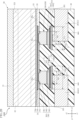
- the semiconductor device A40 of this embodiment differs from the first embodiment in that the lead 10A further includes a receiving plate portion 13 and the lead 20A further includes a receiving plate portion 23.
- FIG. The configuration and operation of other portions of this embodiment are the same as those of the first embodiment. Note that each part of the above first to third embodiments may be combined arbitrarily.
- the lead 10A further includes a receiving plate portion 13.
- the receiving plate portion 13 is interposed between the projecting portion 12 and the metal layer 6 ⁇ /b>A and is connected to the projecting portion 12 .
- the lead 20A further includes a saucer portion 23.
- the receiving plate portion 23 is interposed between the projecting portion 22 and the metal layer 6A and is connected to the projecting portion 22 .
- the shape and dimensions of the saucer portions 13 and 23 are not limited. 6 A of metal layers are formed in contact with the surface which faces the z direction z2 side of the saucer parts 13 and 23. As shown in FIG.
- the saucer portions 13 and 23 are portions that were in contact with the metal layer 6A and could not be completely removed when the projecting portions 12 (22) of the leads 10A (20A) were formed by etching. In this embodiment, it cannot be said that the electrode terminal 36A protrudes from the leads 10 and 20 when viewed in the z direction. However, the electrode terminal 36A protrudes from the body portions 11 and 21 when viewed in the z direction.
- the suspended portion 365a is a portion of the joint surface 365 that does not overlap the main body portion 11 of the lead 10A (the main body portion 21 of the lead 20A).
- the electrode terminal 36A electrically connected to the lead 10A protrudes from the main body portion 11 of the lead 10A in the y direction y2. Further, the electrode terminal 36A electrically connected to the lead 20A protrudes from the body portion 11 of the lead 20A in the y direction y1. That is, the electrode terminal 36A electrically connected to the lead 10A and the electrode terminal 36A electrically connected to the lead 20A are arranged so as to approach each other in the y direction. As a result, the distance between the electrode 34 electrically connected to the lead 10A and the electrode 34 electrically connected to the lead 20A can be reduced, so that the semiconductor device A40 can shorten the current path in the wiring layer and suppress the electrical resistance in the current path. In addition, the semiconductor device A40 has the same effect as the semiconductor device A10 due to the configuration common to the semiconductor device A10.
- FIG. 17 is a diagram for explaining a semiconductor device A50 according to the fifth embodiment of the present disclosure.
- FIG. 17 is a partially enlarged cross-sectional view showing the semiconductor device A50, corresponding to FIG.
- the semiconductor device A50 of this embodiment differs from the first embodiment in that the electrode terminals 36 electrically connected to the leads 20A do not protrude from the leads 20A.
- the configuration and operation of other portions of this embodiment are the same as those of the first embodiment. It should be noted that each part of the above-described first to fourth embodiments may be combined arbitrarily.
- the electrode terminal 36 electrically connected to the lead 20A is not the electrode terminal 36A, and the metal layer 6 formed on the lead 20A is not the metal layer 6A but the metal layer 6B. That is, the lead 20A is the same as the other leads 20, and the electrode terminal 36 electrically connected to the lead 20A does not protrude from the lead 20A.
- the electrode terminal 36A electrically connected to the lead 10A protrudes from the lead 10A in the y direction y2. That is, the electrode terminal 36A electrically connected to the lead 10A is arranged so as to be close to the electrode terminal 36 electrically connected to the lead 20A. Therefore, the distance between the electrode 34 electrically connected to the lead 10A and the electrode 34 electrically connected to the lead 20A is smaller than when the electrode terminal 36 does not protrude from either of the leads 10A and 20A (see FIG. 12). A current path in the wiring layer can be shortened. Thereby, the semiconductor device A50 can suppress the electrical resistance in the current path. Further, the semiconductor device A50 has the same effect as the semiconductor device A10 due to the configuration common to the semiconductor device A10.
- FIG. 18 is a diagram for explaining a semiconductor device A60 according to the sixth embodiment of the present disclosure.
- FIG. 18 is a partially enlarged cross-sectional view showing the semiconductor device A60, corresponding to FIG.
- the semiconductor device A60 of this embodiment differs from the first embodiment in that the metal layer 6A does not protrude from the lead 10A or the lead 20A when viewed in the z direction.
- the configuration and operation of other portions of this embodiment are the same as those of the first embodiment. It should be noted that each part of the above-described first to fifth embodiments may be combined arbitrarily.
- the metal layer 6A does not include the second metal layer 602, but includes only the first metal layer 601. That is, in this embodiment, the metal layer 6A has the same configuration as the metal layer 6B. Moreover, the lead 10A (20A) does not have the projecting portion 12 (22), and the metal layer 6A is formed in contact with the main surface 101 (201). The metal layer 6A is included in the leads 10A and 20A without protruding from the leads 10A and 20A when viewed in the z direction. On the other hand, as in the first embodiment, the electrode terminal 36A electrically connected to the lead 10A protrudes from the lead 10A in the y direction y2.
- the electrode terminal 36A electrically connected to the lead 20A protrudes from the lead 20A to the y-direction y1 side. That is, the electrode terminal 36A electrically connected to the lead 10A and the electrode terminal 36A electrically connected to the lead 20A are arranged so as to approach each other in the y direction. Each electrode terminal 36A is joined to the corresponding metal layer 6A via the joining material 5. As shown in FIG.
- the electrode terminals 36A electrically connected to the leads 10A and the electrode terminals 36A electrically connected to the leads 20A protrude from the leads 10A and 20A, respectively, and are arranged so as to approach each other in the y direction.
- the distance between the electrode 34 electrically connected to the lead 10A and the electrode 34 electrically connected to the lead 20A can be reduced, so that the semiconductor device A60 can shorten the current path in the wiring layer and suppress the electrical resistance in the current path.
- the semiconductor device A60 has the same effect as the semiconductor device A10 due to the configuration common to the semiconductor device A10.
- the electrode terminal 36A may be directly bonded to the principal surface 101 of the lead 10A via the bonding material 5 without forming the metal layer 6A on the lead 10A.
- the metal layer 6A may not be formed on the lead 20A, and the electrode terminal 36A may be directly joined to the main surface 201 of the lead 20A via the joining material 5.
- FIG. 19 is a diagram for explaining a semiconductor device A70 according to the seventh embodiment of the present disclosure.
- FIG. 19 is a plan view showing the semiconductor device A70, corresponding to FIG. In FIG. 19 , for convenience of understanding, the encapsulating resin 40 and the semiconductor element 30 are shown through the encapsulating resin 40 and the semiconductor element 30 by imaginary lines (two-dot chain lines).
- the semiconductor device A70 of this embodiment differs from that of the first embodiment in the shape of the electrode terminal 36 and the metal layer 6 .
- the configuration and operation of other portions of this embodiment are the same as those of the first embodiment. Note that each part of the above first to sixth embodiments may be combined arbitrarily.
- each electrode terminal 36 as viewed in the z-direction is rectangular. Therefore, the joint surface 365 of each electrode terminal 36 also has the same rectangular shape.
- the shape of each metal layer 6 as viewed in the z-direction is rectangular to match the shape of the joint surface 365 of the electrode terminal 36 .
- the electrode terminals 36A electrically connected to the leads 10A and the electrode terminals 36A electrically connected to the leads 20A protrude from the leads 10A and 20A, respectively, and are arranged so as to approach each other in the y direction.
- the distance between the electrode 34 conducting to the lead 10A and the electrode 34 conducting to the lead 20A can be reduced, so that the semiconductor device A70 can shorten the current path in the wiring layer and suppress the electrical resistance in the current path.
- the semiconductor device A70 has the same effect as the semiconductor device A10 due to the configuration common to the semiconductor device A10.
- the z-direction shape (planar shape) and each dimension of the electrode terminal 36 are not limited.
- the shape of each electrode terminal 36 when viewed in the z-direction may be, for example, an elliptical shape, a rectangular shape, or a polygonal shape.
- the electrode terminals 36 may have different shapes or dimensions.
- FIG. 20 is a diagram for explaining a semiconductor device A80 according to the eighth embodiment of the present disclosure.
- FIG. 20 is a partially enlarged cross-sectional view showing the semiconductor device A80, corresponding to FIG.
- the semiconductor device A80 of the present embodiment differs from the first embodiment in that the electrode terminal 36 electrically connected to the lead 10A and the electrode terminal 36 electrically connected to the lead 20A are electrically connected to the same electrode 34.
- FIG. The configuration and operation of other portions of this embodiment are the same as those of the first embodiment. Note that each part of the above first to seventh embodiments may be combined arbitrarily.
- the semiconductor device A80 differs from the semiconductor device A10 in the internal configuration of the semiconductor element 30 and the shape and arrangement of the conductive member 1.
- the leads 10A and 20A are electrically connected through the electrodes 34 of the semiconductor element 30.
- FIG. The electrode terminal 36 electrically connected to the lead 10A and the electrode terminal 36 electrically connected to the lead 20A are in contact with and electrically connected to the same electrode 34, respectively.
- the electrode terminals 36A electrically connected to the leads 10A and the electrode terminals 36A electrically connected to the leads 20A protrude from the leads 10A and 20A, respectively, and are arranged so as to approach each other in the y direction.
- the distance between the position of the electrode 34 at which the electrode terminal 36 conducting to the lead 10A contacts and the position at which the electrode terminal 36 conducting to the lead 20A contacts can be reduced. It can be shortened, and electric resistance in the current path can be suppressed.
- the semiconductor device A80 has the same effect as the semiconductor device A10 due to the configuration common to the semiconductor device A10.
- the semiconductor device according to the present disclosure is not limited to the above-described embodiments.
- the specific configuration of each part of the semiconductor device according to the present disclosure can be changed in various ways.
- the present disclosure includes embodiments described in the appendices below.
- Appendix 1 An element main surface (30a) and an element back surface (30b) facing opposite to each other in the thickness direction, an electrode layer formed on the element main surface, and being in contact with the electrode layer and protruding in the thickness direction a semiconductor element (30) having electrode terminals (36A); a first lead (10A) electrically connected to the semiconductor element and having a first main surface (101) and a first rear surface (102) facing opposite sides in the thickness direction; a sealing resin (40) covering the semiconductor element; with The first lead has a first body portion (11) located closer to the first rear surface than the first principal surface, The electrode terminal has a joint surface (365) facing the first lead, The semiconductor device according to claim 1, wherein the bonding surface has a suspended portion (365a) that does not overlap the first body portion when viewed in the thickness direction.
- Appendix 2 The semiconductor device according to appendix 1, wherein the suspended portion does not overlap the first lead when viewed in the thickness direction. Appendix 3. 3. The semiconductor device according to appendix 1 or 2, wherein the area of the suspended portion is 10% or more and 50% or less of the area of the bonding surface. Appendix 4. 4. The semiconductor device according to any one of appendices 1 to 3, further comprising a metal layer (6A) formed on the first lead and to which the electrode terminal is joined. Appendix 5. 5. The semiconductor device according to appendix 4, wherein the metal layer includes a metal layer suspending portion (6Aa) that does not overlap the first body portion when viewed in the thickness direction. Appendix 6.
- said metal layer comprises a first metal layer (601) and a second metal layer (602); the second metal layer is in contact with the first lead; 6.
- the semiconductor device according to appendix 4 or 5 wherein the first metal layer is in contact with the second metal layer and is included in the second metal layer when viewed in the thickness direction.
- Appendix 7. The semiconductor device according to any one of Appendixes 4 to 6, wherein the shape of the metal layer when viewed in the thickness direction and the shape of the bonding surface are circular. Supplementary Note 8, Third Embodiment, FIG. 8. The semiconductor device according to any one of Appendixes 4 to 7, wherein the metal layer is arranged in contact with the first main surface. Appendix 9.
- the first lead has a projecting portion (12) projecting from the first main surface in the thickness direction and overlapping the bonding surface when viewed in the thickness direction; 8.
- Appendix 10. further comprising a bonding material (5) interposed between the bonding surface and the first lead; 10.
- a second lead (20A) which is spaced apart from the first lead and conducts to the semiconductor element and has a second main surface (201) and a second rear surface (202) facing opposite to each other in the thickness direction; further prepared, the second lead has a second body portion (21) located closer to the second rear surface than the second main surface;
- the semiconductor element has a second electrode terminal (36A) that is in contact with the electrode layer and protrudes in the thickness direction,
- the second electrode terminal has a second joint surface (365) facing the second lead, 11.
- the semiconductor device according to any one of appendices 1 to 10, wherein the second bonding surface includes a second suspended portion (365A) that does not overlap the second body portion when viewed in the thickness direction. Appendix 12. 12.
- said electrode layer comprising a first electrode (34) and a second electrode (34) spaced apart from each other; the electrode terminal is in contact with the first electrode; the second electrode terminal is in contact with the second electrode; 13.
- the semiconductor element comprises a switching element having a first terminal, a second terminal, and a control terminal, the first electrode is electrically connected to the first terminal of the switching element; 14.
- the electrode layer comprises a first electrode (34); 13.
- the semiconductor device according to appendix 11 or 12 wherein the electrode terminal and the second electrode terminal are in contact with the first electrode.
Abstract
A semiconductor device A10 comprises: a semiconductor element 30 having an element main surface 30a and an element back surface 30b facing sides opposite to each other in a z direction, electrodes 34 formed on the element main surface 30a, and electrode terminals 36A that are in contact with the electrodes 34 and that protrude in the z direction; a lead 10A that has a main surface 101 and a back surface 102 facing sides opposite to each other in the z direction and that makes electrical connection to the semiconductor element 30; and a sealing resin 40 that covers the semiconductor element 30. The lead 10A has a body part 11 located closer to the back surface 102 than to the main surface 101. The electrode terminals 36A each have a joining surface 365 facing the lead 10. The joining surface 365 has a hanging part 365a not overlapping the body part 11 when viewed in the z direction.
Description
本開示は、半導体装置に関する。
The present disclosure relates to semiconductor devices.
複数のリードと半導体素子とが、いわゆるフリップチップの形態で接合された半導体装置が提案されている。このような半導体装置は、たとえば特許文献1に開示されている。当該半導体装置は、複数のリード、半導体素子、接合層、および封止樹脂を備えている。半導体素子は、複数の第1電極をリードに対向させて、リードに搭載されている。各第1電極は、半導体層に導通する基部、および、基部からリードに向けて突出する円柱状の柱状部を備えている。柱状部は、接合層を介して、リードに接合されている。複数のリードは互いに所定以上の間隔を空けて配置されている。半導体素子において、あるリードに接合される第1電極と、別のリードに接合される第1電極とは、リード間の距離に応じて離れて形成される。第1電極間の距離が長くなると、半導体層内部に形成される電流経路が長くなるので、電流経路での電気抵抗が大きくなる。
A semiconductor device has been proposed in which a plurality of leads and a semiconductor element are bonded in the form of a so-called flip chip. Such a semiconductor device is disclosed in Patent Document 1, for example. The semiconductor device includes multiple leads, a semiconductor element, a bonding layer, and a sealing resin. The semiconductor element is mounted on the leads with the plurality of first electrodes facing the leads. Each first electrode has a base electrically connected to the semiconductor layer and a columnar portion projecting from the base toward the lead. The columnar portion is joined to the lead via the joining layer. A plurality of leads are arranged with a predetermined interval or more from each other. In a semiconductor device, a first electrode joined to a certain lead and a first electrode joined to another lead are separated from each other according to the distance between the leads. As the distance between the first electrodes increases, the electric resistance in the current path increases because the current path formed inside the semiconductor layer increases.
本開示は、従来より改良が施された半導体装置を提供することを一の課題とする。特に本開示は、上記した事情に鑑み、電流経路での電気抵抗を抑制できる半導体装置を提供することをその一の課題とする。
An object of the present disclosure is to provide an improved semiconductor device. In particular, in view of the circumstances described above, an object of the present disclosure is to provide a semiconductor device capable of suppressing electrical resistance in a current path.
本開示の一の側面によって提供される半導体装置は、厚さ方向において互いに反対側を向く素子主面および素子裏面と、前記素子主面に形成された電極層と、前記電極層に接し、かつ、前記厚さ方向に突出する電極端子と、を有する半導体素子と、前記半導体素子に導通し、かつ、前記厚さ方向において互いに反対側を向く第1主面および第1裏面を有する第1リードと、前記半導体素子を覆う封止樹脂と、を備える。前記第1リードは、前記第1主面より前記第1裏面側に位置する第1本体部をさらに有する。前記電極端子は、前記第1リードに対向する接合面を備える。前記接合面は、前記厚さ方向に視て前記第1本体部に重ならない宙吊部を備えている。
A semiconductor device provided according to one aspect of the present disclosure includes an element main surface and an element back surface facing opposite sides in a thickness direction, an electrode layer formed on the element main surface, in contact with the electrode layer, and and electrode terminals projecting in the thickness direction; and a first lead electrically connected to the semiconductor element and having a first main surface and a first back surface facing opposite to each other in the thickness direction. and a sealing resin that covers the semiconductor element. The first lead further has a first main body positioned closer to the first rear surface than the first main surface. The electrode terminal has a bonding surface facing the first lead. The joint surface has a suspended portion that does not overlap the first body portion when viewed in the thickness direction.
上記構成によれば、電流経路での電気抵抗を抑制可能な半導体装置を提供することが可能である。
According to the above configuration, it is possible to provide a semiconductor device capable of suppressing electrical resistance in the current path.
本開示のその他の特徴および利点は、添付図面を参照して以下に行う詳細な説明によって、より明らかとなろう。
Other features and advantages of the present disclosure will become clearer from the detailed description given below with reference to the accompanying drawings.
以下、本開示の好ましい実施の形態を、添付図面を参照して具体的に説明する。
Preferred embodiments of the present disclosure will be specifically described below with reference to the accompanying drawings.
第1実施形態:
図1~図13は、本開示に係る半導体装置の一例を示している。本実施形態の半導体装置A10は、複数のリード10、複数のリード20、複数のリード25、複数のリード26、リード27、複数の接合材5、複数の金属層6、半導体素子30、および封止樹脂40を備えている。半導体装置A10のパッケージ形式は、特に限定されず、本実施形態においては、図1に示すように、QFN(Quad Flat Non-leaded package)タイプである。また、半導体装置A10の用途や機能は、何ら限定されない。たとえば、半導体装置A10は、DC/DCコンバータの回路を構成する一要素に用いられる。 First embodiment:
1 to 13 show an example of a semiconductor device according to the present disclosure. The semiconductor device A10 of this embodiment includes a plurality ofleads 10, a plurality of leads 20, a plurality of leads 25, a plurality of leads 26, a lead 27, a plurality of bonding materials 5, a plurality of metal layers 6, a semiconductor element 30, and a sealing. A stopper resin 40 is provided. The package format of the semiconductor device A10 is not particularly limited, and in this embodiment, as shown in FIG. 1, it is a QFN (Quad Flat Non-leaded package) type. Further, the usage and function of the semiconductor device A10 are not limited at all. For example, the semiconductor device A10 is used as one element forming a circuit of a DC/DC converter.
図1~図13は、本開示に係る半導体装置の一例を示している。本実施形態の半導体装置A10は、複数のリード10、複数のリード20、複数のリード25、複数のリード26、リード27、複数の接合材5、複数の金属層6、半導体素子30、および封止樹脂40を備えている。半導体装置A10のパッケージ形式は、特に限定されず、本実施形態においては、図1に示すように、QFN(Quad Flat Non-leaded package)タイプである。また、半導体装置A10の用途や機能は、何ら限定されない。たとえば、半導体装置A10は、DC/DCコンバータの回路を構成する一要素に用いられる。 First embodiment:
1 to 13 show an example of a semiconductor device according to the present disclosure. The semiconductor device A10 of this embodiment includes a plurality of
図1は、半導体装置A10を示す斜視図である。図2は、半導体装置A10を示す平面図である。図2においては、理解の便宜上、封止樹脂40を透過して、封止樹脂40の外形を想像線(二点鎖線)で示している。図3は、半導体装置A10を示す平面図である。図3においては、理解の便宜上、封止樹脂40および半導体素子30を透過して、封止樹脂40および半導体素子30の外形を想像線(二点鎖線)で示している。図4は、半導体装置A10を示す底面図である。図5は、半導体装置A10を示す正面図である。図6は、半導体装置A10を示す背面図である。図7は、半導体装置A10を示す右側面図である。図8は、半導体装置A10を示す左側面図である。図9は、図3のIX-IX線に沿う断面図である。図10は、図3のX-X線に沿う断面図である。図11は、図3のXI-XI線に沿う断面図である。図12は、図9の部分拡大図である。図13は、図9の部分拡大図である。
FIG. 1 is a perspective view showing the semiconductor device A10. FIG. 2 is a plan view showing the semiconductor device A10. In FIG. 2 , for convenience of understanding, the outer shape of the sealing resin 40 is shown by an imaginary line (chain double-dashed line) through the sealing resin 40 . FIG. 3 is a plan view showing the semiconductor device A10. In FIG. 3 , for convenience of understanding, the encapsulating resin 40 and the semiconductor element 30 are shown through the encapsulating resin 40 and the semiconductor element 30 by imaginary lines (double-dot chain lines). FIG. 4 is a bottom view showing the semiconductor device A10. FIG. 5 is a front view showing the semiconductor device A10. FIG. 6 is a back view showing the semiconductor device A10. FIG. 7 is a right side view showing the semiconductor device A10. FIG. 8 is a left side view of the semiconductor device A10. 9 is a cross-sectional view taken along line IX-IX in FIG. 3. FIG. 10 is a cross-sectional view taken along line XX of FIG. 3. FIG. FIG. 11 is a cross-sectional view along line XI-XI in FIG. 12 is a partially enlarged view of FIG. 9. FIG. 13 is a partially enlarged view of FIG. 9. FIG.
半導体装置A10は、板状であり、厚さ方向視(平面視)の形状が長矩形状である。説明の便宜上、半導体装置A10の「厚さ方向」(平面視方向)の一例をz方向とし、z方向に直交する半導体装置A10の短辺に沿う方向(図2~図4における上下方向)の一例をx方向、z方向およびx方向に直交する方向(図2~図4における左右方向)の一例をy方向とする。また、z方向の一方側(図5~図8における下側)をz1側とし、他方側(図5~図8における上側)をz2側とする。x方向の一方側(図2および図3における下側)をx1側とし、他方側(図2および図3における上側)をx2側とする。y方向の一方側(図2~図4における左側)をy1側とし、他方側(図2~図4における右側)をy2側とする。z方向が本開示の「厚さ方向」の一例に相当する。なお、半導体装置A10の形状および各寸法は限定されない。
The semiconductor device A10 is plate-shaped, and has a long rectangular shape when viewed in the thickness direction (planar view). For convenience of explanation, an example of the “thickness direction” (planar view direction) of the semiconductor device A10 is defined as the z-direction, and the direction along the short side of the semiconductor device A10 orthogonal to the z-direction (vertical direction in FIGS. 2 to 4). An example is the x-direction, the z-direction, and the y-direction is an example of a direction perpendicular to the x-direction (horizontal direction in FIGS. 2 to 4). One side in the z direction (the lower side in FIGS. 5 to 8) is the z1 side, and the other side (the upper side in FIGS. 5 to 8) is the z2 side. One side in the x direction (the lower side in FIGS. 2 and 3) is the x1 side, and the other side (the upper side in FIGS. 2 and 3) is the x2 side. One side in the y direction (the left side in FIGS. 2 to 4) is the y1 side, and the other side (the right side in FIGS. 2 to 4) is the y2 side. The z direction corresponds to an example of the "thickness direction" of the present disclosure. The shape and dimensions of the semiconductor device A10 are not limited.
複数のリード10、複数のリード20、複数のリード25、複数のリード26、およびリード27は、互いに離間して配置されている。複数のリード10、複数のリード20、複数のリード25、複数のリード26、およびリード27は、図2に示すように、半導体素子30を支持するとともに、半導体装置A10を配線基板に実装するための端子をなしている。図9~図11に示すように、複数のリード10、複数のリード20、複数のリード25、複数のリード26、およびリード27の各々は、その一部が封止樹脂40に覆われている。図1、図4~図8においては、複数のリード10、複数のリード20、複数のリード25、複数のリード26、およびリード27のうち封止樹脂40から露出する部分に、複数の離散点からなるハッチングを付している。以下では、複数のリード10、複数のリード20、複数のリード25、複数のリード26、およびリード27をまとめて示す場合、「導電部材1」と記載する場合がある。
The plurality of leads 10, the plurality of leads 20, the plurality of leads 25, the plurality of leads 26, and the leads 27 are arranged apart from each other. The plurality of leads 10, the plurality of leads 20, the plurality of leads 25, the plurality of leads 26, and the leads 27 support the semiconductor element 30 and mount the semiconductor device A10 on the wiring substrate, as shown in FIG. terminal. As shown in FIGS. 9 to 11, each of the plurality of leads 10, the plurality of leads 20, the plurality of leads 25, the plurality of leads 26, and the leads 27 is partially covered with a sealing resin 40. . 1, 4 to 8, a plurality of discrete points are formed on portions of the plurality of leads 10, the plurality of leads 20, the plurality of leads 25, the plurality of leads 26, and the leads 27 exposed from the sealing resin 40. The hatching consisting of Hereinafter, when the plurality of leads 10, the plurality of leads 20, the plurality of leads 25, the plurality of leads 26, and the leads 27 are collectively indicated, they may be described as "conductive member 1".
導電部材1は、たとえば、金属板にエッチング加工を施すことで形成されたリードフレームから構成されている。なお、導電部材1の形成方法は限定されない。導電部材1の構成材料は、たとえば、CuまたはCu合金であるが、これに限定されない。
The conductive member 1 is composed of, for example, a lead frame formed by etching a metal plate. Note that the method for forming the conductive member 1 is not limited. A constituent material of the conductive member 1 is, for example, Cu or a Cu alloy, but is not limited thereto.
複数(本実施形態では4個)のリード10は、図3および図4に示すように、各々がx方向に延びている。複数のリード10は、y方向に所定の間隔を隔てて配列されている。複数のリード10の各々は、半導体装置A10において電力変換対象となる直流電力(電圧)が入力される入力端子である。リード10は、正極(P端子)である。
A plurality of (four in this embodiment) leads 10 each extend in the x direction, as shown in FIGS. A plurality of leads 10 are arranged at predetermined intervals in the y direction. Each of the plurality of leads 10 is an input terminal to which DC power (voltage) to be converted in the semiconductor device A10 is input. The lead 10 is a positive electrode (P terminal).
図9および図10に示すようにリード10は、主面101、2個の裏面102、凹面103、および2個の端面104を有する。主面101および裏面102は、z方向において互いに反対側を向く。主面101は、z方向z2側を向き、かつ、半導体素子30に対向している。主面101は、封止樹脂40に覆われている。各リード10において、半導体素子30は、主面101に支持されている。裏面102は、z方向z1側を向き、封止樹脂40から露出している。図4に示すように、2個の裏面102は、リード10のx方向両端部にそれぞれ配置されている。凹面103は、x方向において、2個の裏面102の間に位置する。凹面103は、z方向において、裏面102に対して主面101側(z方向z2側)に位置する。凹面103は、封止樹脂40に覆われている。リード10は、本実施形態では、裏面102が位置する部分の幅寸法(y方向の寸法)が、凹面103が位置する部分の幅寸法(y方向の寸法)より大きい。端面104は、主面101および裏面102の双方につながっている。一方の端面104は、リード10のx方向x1側端部に位置し、x方向x1側を向いている。他方の端面104は、リード10のx方向x2側端部に位置し、x方向x2側を向いている。各端面104は、封止樹脂40から露出している。
As shown in FIGS. 9 and 10, the lead 10 has a main surface 101, two back surfaces 102, a concave surface 103, and two end surfaces 104. The main surface 101 and the back surface 102 face opposite sides in the z-direction. The main surface 101 faces the z-direction z2 side and faces the semiconductor element 30 . Main surface 101 is covered with sealing resin 40 . In each lead 10 , the semiconductor element 30 is supported on the main surface 101 . The back surface 102 faces the z-direction z1 side and is exposed from the sealing resin 40 . As shown in FIG. 4, the two back surfaces 102 are arranged at both ends of the lead 10 in the x direction. A concave surface 103 is located between the two back surfaces 102 in the x-direction. The concave surface 103 is positioned on the principal surface 101 side (z2 side in the z direction) with respect to the back surface 102 in the z direction. The concave surface 103 is covered with the sealing resin 40 . In the present embodiment, the lead 10 has a width dimension (y-direction dimension) of a portion where the back surface 102 is located larger than a width dimension (y-direction dimension) of a portion where the concave surface 103 is located. End surface 104 is connected to both main surface 101 and back surface 102 . One end face 104 is positioned at the end of the lead 10 on the x1 side in the x direction and faces the x1 side. The other end face 104 is located at the end of the lead 10 on the x2 side in the x direction and faces the x2 side. Each end face 104 is exposed from the sealing resin 40 .
複数のリード10は、リード10Aを含む。リード10Aは、複数のリード10の中で、最もx方向x1側に位置している。リード10Aは、図13に示すように、本体部11および突出部12を備えている。本体部11は、主面101より裏面102側(z方向z1側)に位置する部分である。突出部12は、主面101からz方向z2側に突出した部分である。突出部12は、z方向に視て、後述する電極端子36の接合面365に重なっている。
The plurality of leads 10 includes leads 10A. Among the plurality of leads 10, the lead 10A is positioned closest to the x1 side in the x direction. The lead 10A has a body portion 11 and a projecting portion 12, as shown in FIG. The body portion 11 is a portion located on the back surface 102 side (z direction z1 side) from the main surface 101 . The protrusion 12 is a portion that protrudes from the main surface 101 in the z direction z2. The projecting portion 12 overlaps a joint surface 365 of the electrode terminal 36, which will be described later, when viewed in the z direction.
複数(本実施形態では3個)のリード20は、図3および図4に示すように、各々がx方向に延びている。本実施形態において、複数のリード20は、y方向に所定の間隔を隔てて配列されている。各リード20は、y方向において隣り合うリード10の間にそれぞれ配置されている。複数のリード10および複数のリード20は、y方向において交互に配列されている。複数のリード20の各々は、半導体素子30に構成された後述するスイッチング回路321により電力変換された交流電力(電圧)が出力される。
A plurality of (three in this embodiment) leads 20 each extend in the x direction, as shown in FIGS. In this embodiment, the plurality of leads 20 are arranged at predetermined intervals in the y direction. Each lead 20 is arranged between leads 10 adjacent in the y direction. The plurality of leads 10 and the plurality of leads 20 are alternately arranged in the y direction. Each of the plurality of leads 20 outputs AC power (voltage) that is power-converted by a switching circuit 321 (described later) formed in the semiconductor element 30 .
図9および図11に示すように、リード20は、主面201、裏面202、凹面203、および2個の端面204を有する。主面201および裏面202は、z方向において互いに反対側を向く。主面201は、z方向z2側を向き、かつ、半導体素子30に対向している。主面201は、封止樹脂40に覆われている。各リード20において、半導体素子30は、主面201に支持されている。裏面202は、z方向z1側を向き、封止樹脂40から露出している。図4に示すように、裏面202は、リード20のx方向中央に配置されている。裏面202は、y方向に視て、複数のリード10の各裏面102のいずれにも重なっていない。凹面203は、裏面202を囲み、リード20のx方向両端まで延びている。凹面203は、z方向において、裏面202に対して主面201側(z方向z2側)に位置する。凹面203は、封止樹脂40に覆われている。リード20は、本実施形態では、裏面202が位置する部分の幅寸法(y方向の寸法)が、裏面202が位置しない部分の幅寸法(y方向の寸法)より大きい。端面204は、主面201および凹面203の双方につながっている。一方の端面204は、リード20のx方向x1側端部に位置し、x方向x1側を向いている。他方の端面204は、リード20のx方向x2側端部に位置し、x方向x2側を向いている。各端面204は、封止樹脂40から露出している。
As shown in FIGS. 9 and 11, the lead 20 has a main surface 201, a back surface 202, a concave surface 203, and two end surfaces 204. The main surface 201 and the back surface 202 face opposite sides in the z-direction. The main surface 201 faces the z-direction z2 side and faces the semiconductor element 30 . Main surface 201 is covered with sealing resin 40 . In each lead 20 , semiconductor element 30 is supported on main surface 201 . The back surface 202 faces the z-direction z1 side and is exposed from the sealing resin 40 . As shown in FIG. 4, the back surface 202 is arranged in the center of the lead 20 in the x direction. The back surface 202 does not overlap any of the back surfaces 102 of the leads 10 when viewed in the y direction. The concave surface 203 surrounds the back surface 202 and extends to both ends of the lead 20 in the x direction. The concave surface 203 is positioned on the principal surface 201 side (z2 side in the z direction) with respect to the back surface 202 in the z direction. The concave surface 203 is covered with the sealing resin 40 . In this embodiment, the width dimension (dimension in the y direction) of the portion of the lead 20 where the back surface 202 is located is larger than the width dimension (dimension in the y direction) of the portion where the back surface 202 is not located. End surface 204 is connected to both main surface 201 and concave surface 203 . One end surface 204 is located at the end of the lead 20 on the x1 side in the x direction and faces the x1 side. The other end face 204 is positioned at the end of the lead 20 on the x2 direction side and faces the x2 direction side. Each end surface 204 is exposed from the sealing resin 40 .
複数のリード20は、リード20Aを含む。リード20Aは、複数のリード20の中で、最もy方向y1側に位置しており、リード10Aに隣接して、リード10Aのy方向y2側に位置している。リード20Aは、図13に示すように、本体部21および突出部22を備えている。本体部21は、主面201より裏面202側(z方向z1側)に位置する部分である。突出部22は、主面201からz方向z2側に突出した部分である。
The plurality of leads 20 includes leads 20A. The lead 20A is positioned closest to the y-direction y1 side among the plurality of leads 20, and is adjacent to the lead 10A and positioned on the y-direction y2 side of the lead 10A. The lead 20A has a body portion 21 and a projecting portion 22, as shown in FIG. The body portion 21 is a portion located on the back surface 202 side (z direction z1 side) from the main surface 201 . The protrusion 22 is a portion that protrudes from the main surface 201 in the z direction z2.
複数(本実施形態では4個)のリード25は、図3に示すように、リード10Aよりもy方向y1側に位置し、半導体装置A10のy方向y1側の端部に位置する。複数のリード25の各々には、たとえば後述する制御回路322を駆動させるための電力(電圧)、または、制御回路322に伝達するための電気信号が入力される。図3、図4、および図9に示すように、リード25は、主面251、裏面252、および端面254を有する。主面251および裏面252は、z方向において互いに反対側を向く。主面251は、z方向z2側を向き、かつ半導体素子30に対向している。主面251は、封止樹脂40に覆われている。各リード25において、半導体素子30は、主面251に支持されている。裏面252は、z方向z1側を向き、封止樹脂40から露出している。図4に示すように、裏面252は、リード25のy方向y1側端部に配置されている。端面254は、主面251および裏面252の双方につながっている。端面254は、リード25のy方向y1側端部に位置し、y方向y1側を向いている。端面254は、封止樹脂40から露出している。図8に示すように、複数のリード25の端面254は、x方向に沿って所定の間隔で配列されている。
As shown in FIG. 3, the plurality of (four in this embodiment) leads 25 are located on the y-direction y1 side of the leads 10A, and are located at the end of the semiconductor device A10 on the y-direction y1 side. Power (voltage) for driving a control circuit 322, which will be described later, or an electric signal for transmission to the control circuit 322 is input to each of the leads 25, for example. As shown in FIGS. 3, 4 and 9, lead 25 has major surface 251 , back surface 252 and end surface 254 . The main surface 251 and the back surface 252 face opposite sides in the z-direction. The main surface 251 faces the z-direction z2 side and faces the semiconductor element 30 . The main surface 251 is covered with the sealing resin 40 . In each lead 25 , semiconductor element 30 is supported on main surface 251 . The rear surface 252 faces the z-direction z1 side and is exposed from the sealing resin 40 . As shown in FIG. 4, the rear surface 252 is arranged at the end of the lead 25 on the y1 side in the y direction. End surface 254 is connected to both main surface 251 and back surface 252 . The end face 254 is positioned at the end of the lead 25 on the y1 side in the y direction and faces the y1 side in the y direction. The end surface 254 is exposed from the sealing resin 40 . As shown in FIG. 8, the end faces 254 of the multiple leads 25 are arranged at predetermined intervals along the x direction.
複数(本実施形態では4個)のリード26は、図3に示すように、y方向において、リード10Aと複数のリード25との間に位置する。複数のリード26の一部(本実施形態では2個)は、半導体装置A10のx方向x1側の端部に位置する。他のリード26(本実施形態では2個)は、半導体装置A10のx方向x2側の端部に位置する。複数のリード26の各々には、たとえば制御回路322に伝達するための電気信号が入力される。図3および図4に示すように、リード26は、主面261、裏面262、および端面264を有する。主面261および裏面262は、z方向において互いに反対側を向く。主面261は、z方向z2側を向き、かつ半導体素子30に対向している。主面261は、封止樹脂40に覆われている。各リード26において、半導体素子30は、主面261に支持されている。裏面262は、z方向z1側を向き、封止樹脂40から露出している。図4に示すように、裏面262は、リード26のx方向外側端部に配置されている。端面264は、主面261および裏面262の双方につながっている。端面264は、リード26のx方向外側端部に位置し、x方向外側を向いている。端面264は、封止樹脂40から露出している。図5および図6に示すように、端面264は、リード10の端面104およびリード20の端面204とともに、y方向に沿って配列されている。
A plurality of (four in this embodiment) leads 26 are positioned between the lead 10A and the plurality of leads 25 in the y direction, as shown in FIG. Some of the plurality of leads 26 (two in this embodiment) are positioned at the end of the semiconductor device A10 on the x-direction x1 side. Other leads 26 (two in this embodiment) are located at the end of the semiconductor device A10 on the x-direction x2 side. An electrical signal is input to each of the leads 26 for transmission to the control circuit 322, for example. As shown in FIGS. 3 and 4, lead 26 has major surface 261 , back surface 262 and end surface 264 . The main surface 261 and the back surface 262 face opposite sides in the z-direction. The main surface 261 faces the z-direction z2 side and faces the semiconductor element 30 . The main surface 261 is covered with the sealing resin 40 . In each lead 26 , semiconductor element 30 is supported on main surface 261 . The back surface 262 faces the z-direction z1 side and is exposed from the sealing resin 40 . As shown in FIG. 4, the back surface 262 is located at the x-direction outer end of the lead 26 . End surface 264 is connected to both main surface 261 and back surface 262 . The end face 264 is positioned at the x-direction outer end of the lead 26 and faces outward in the x-direction. The end surface 264 is exposed from the sealing resin 40 . As shown in FIGS. 5 and 6, the end faces 264 are arranged along the y-direction along with the end faces 104 of the leads 10 and the end faces 204 of the leads 20 .
リード27は、図3に示すように、複数のリード10よりもy方向y2側に位置する。リード27は、半導体装置A10において電力変換対象となる直流電力(電圧)が入力される入力端子である。リード27は、負極(N端子)である。図3、図4、図9に示すように、リード27は、主面271、複数の裏面272、凹面273、および複数の端面274を有する。主面271および裏面272は、z方向において互いに反対側を向く。主面271は、z方向z2側を向き、かつ半導体素子30に対向している。主面271は、封止樹脂40に覆われている。リード27において、半導体素子30は、主面271に支持されている。裏面272は、z方向z1側を向き、封止樹脂40から露出している。図4に示すように、裏面272は、リード27のy方向y2側端部に配置されている。複数(本実施形態では4個)の裏面272は、x方向において互いに離間して、x方向に沿って所定の間隔で配列されている。凹面273は、リード27においてy方向y1側寄りに位置する。凹面273は、z方向において、裏面272に対して主面271側(z方向z2側)に位置する。凹面273は、封止樹脂40に覆われている。各端面274は、主面271およびいずれかの裏面272の双方につながっている。端面274は、リード27のy方向y2側端部に位置し、y方向y2側を向いている。端面264は、封止樹脂40から露出している。図7に示すように、複数の端面274は、x方向に沿って所定の間隔で配列されている。
The leads 27 are located on the y2 side in the y direction with respect to the plurality of leads 10, as shown in FIG. The lead 27 is an input terminal to which DC power (voltage) to be converted in the semiconductor device A10 is input. The lead 27 is a negative electrode (N terminal). As shown in FIGS. 3, 4 and 9, the lead 27 has a major surface 271 , a plurality of back surfaces 272 , a concave surface 273 and a plurality of end surfaces 274 . The main surface 271 and the back surface 272 face opposite sides in the z-direction. The main surface 271 faces the z-direction z2 side and faces the semiconductor element 30 . The main surface 271 is covered with the sealing resin 40 . The semiconductor element 30 is supported on the main surface 271 of the leads 27 . The back surface 272 faces the z-direction z1 side and is exposed from the sealing resin 40 . As shown in FIG. 4, the rear surface 272 is arranged at the end of the lead 27 on the y2 side in the y direction. A plurality of (four in this embodiment) rear surfaces 272 are spaced apart from each other in the x direction and arranged at predetermined intervals along the x direction. The concave surface 273 is positioned closer to the y1 side of the lead 27 in the y direction. The concave surface 273 is located on the main surface 271 side (z2 side in the z direction) with respect to the back surface 272 in the z direction. The concave surface 273 is covered with the sealing resin 40 . Each end surface 274 is connected to both the main surface 271 and one of the back surfaces 272 . The end face 274 is located at the end of the lead 27 on the y2 side in the y direction and faces the y2 side in the y direction. The end surface 264 is exposed from the sealing resin 40 . As shown in FIG. 7, the plurality of end surfaces 274 are arranged at predetermined intervals along the x direction.
各リード10の裏面102および端面104、各リード20の裏面202および端面204、各リード25の裏面252および端面254、各リード26の裏面262および端面264、ならびに、リード27の裏面272および端面274には、たとえばSnめっきを施してもよい。なお、Snめっきに替えて、たとえばNi、Pd、Auの順に積層された複数の金属めっきを採用してもよい。また、リード10、リード20、リード25、リード26、およびリード27のそれぞれの数、形状、および配置は限定されない。
Back surface 102 and end surface 104 of each lead 10, back surface 202 and end surface 204 of each lead 20, back surface 252 and end surface 254 of each lead 25, back surface 262 and end surface 264 of each lead 26, and back surface 272 and end surface 274 of lead 27. may be plated with Sn, for example. Instead of the Sn plating, a plurality of metal platings in which Ni, Pd, and Au are laminated in this order, for example, may be adopted. Also, the number, shape, and arrangement of leads 10, 20, 25, 26, and 27 are not limited.
半導体素子30は、図2に示すように、z方向視において、半導体装置A10の中央に配置されている。半導体素子30は、図9~図11に示すように、複数のリード10、複数のリード20、複数のリード25、複数のリード26、およびリード27に支持されている。半導体素子30は、封止樹脂40に覆われている。半導体素子30は、半導体基板31、半導体層32、パッシベーション膜33、電極34、絶縁層35、および複数の電極端子36を有する。半導体素子30は、その内部に回路が構成されたフリップチップ型のLSIである。
As shown in FIG. 2, the semiconductor element 30 is arranged in the center of the semiconductor device A10 when viewed in the z direction. The semiconductor element 30 is supported by a plurality of leads 10, a plurality of leads 20, a plurality of leads 25, a plurality of leads 26, and a lead 27, as shown in FIGS. The semiconductor element 30 is covered with a sealing resin 40 . The semiconductor element 30 has a semiconductor substrate 31 , a semiconductor layer 32 , a passivation film 33 , an electrode 34 , an insulating layer 35 and a plurality of electrode terminals 36 . The semiconductor element 30 is a flip-chip type LSI in which a circuit is configured.
半導体素子30は、図2に示すようにz方向視長矩形状であり、図9~図11に示すように板状である。半導体素子30は、素子主面30aおよび素子裏面30bを有する。素子主面30aは、z方向において、複数のリード10の主面101、複数のリード20の主面201、複数のリード25の主面251、複数のリード26の主面261、およびリード27の主面271と対向している。素子裏面30bは、z方向において素子主面30aとは反対側を向いている。
The semiconductor element 30 has a rectangular shape when viewed in the z direction as shown in FIG. 2, and a plate shape as shown in FIGS. The semiconductor element 30 has an element main surface 30a and an element rear surface 30b. The element main surface 30a includes the main surface 101 of the plurality of leads 10, the main surface 201 of the plurality of leads 20, the main surface 251 of the plurality of leads 25, the main surface 261 of the plurality of leads 26, and the main surface 261 of the plurality of leads 27 in the z direction. It faces the main surface 271 . The element rear surface 30b faces the side opposite to the element main surface 30a in the z direction.
図12および図13に示すように、半導体基板31は、そのz方向z1側に半導体層32、パッシベーション膜33、電極34、絶縁層35、および複数の電極端子36が設けられている。半導体基板31の構成材料は、たとえば、Si(シリコン)またはSiC(炭化ケイ素)である。本実施形態においては、半導体基板31のz方向z2側の面が、素子裏面30bを構成している。
As shown in FIGS. 12 and 13, the semiconductor substrate 31 is provided with a semiconductor layer 32, a passivation film 33, an electrode 34, an insulating layer 35, and a plurality of electrode terminals 36 on the z-direction z1 side. The constituent material of the semiconductor substrate 31 is, for example, Si (silicon) or SiC (silicon carbide). In this embodiment, the surface of the semiconductor substrate 31 on the z-direction z2 side constitutes the element back surface 30b.
図9~図13に示すように、半導体層32は、半導体基板31のz方向z1側に積層されている。半導体層32は、ドープされる元素量の相違に基づく複数種類のp型半導体およびn型半導体を含む。半導体層32には、スイッチング回路321と、スイッチング回路321に導通する制御回路322とが構成されている。スイッチング回路321は、MOSFET(Metal-Oxide-Semiconductor Field-Effect Transistor)またはIGBT(Insulated Gate Bipolar Transistor)などのスイッチング素子を複数備えている。半導体装置A10が示す例においては、スイッチング回路321は、高電圧領域(上アーム回路)と低電圧領域(下アーム回路)との2個の領域に区分されている。各々の領域は、たとえばnチャンネル型のMOSFETを備えている。制御回路322は、スイッチング回路321を駆動させるためのゲートドライバや、スイッチング回路321の高電圧領域に対応するブートストラップ回路などが構成されるとともに、スイッチング回路321を正常に駆動させるための制御を行う。なお、半導体層32には、配線層(図示略)がさらに構成されている。当該配線層により、スイッチング回路321と制御回路322とは、相互に導通している。
As shown in FIGS. 9 to 13, the semiconductor layer 32 is laminated on the semiconductor substrate 31 on the z-direction z1 side. The semiconductor layer 32 includes a plurality of types of p-type semiconductors and n-type semiconductors based on different amounts of doped elements. A switching circuit 321 and a control circuit 322 electrically connected to the switching circuit 321 are formed in the semiconductor layer 32 . The switching circuit 321 includes a plurality of switching elements such as MOSFETs (Metal-Oxide-Semiconductor Field-Effect Transistors) or IGBTs (Insulated Gate Bipolar Transistors). In the example shown by the semiconductor device A10, the switching circuit 321 is divided into two regions, a high voltage region (upper arm circuit) and a low voltage region (lower arm circuit). Each region comprises, for example, an n-channel MOSFET. The control circuit 322 includes a gate driver for driving the switching circuit 321, a bootstrap circuit corresponding to the high voltage region of the switching circuit 321, and the like, and performs control for normally driving the switching circuit 321. . A wiring layer (not shown) is further formed in the semiconductor layer 32 . The wiring layer electrically connects the switching circuit 321 and the control circuit 322 to each other.
図12および図13に示すように、パッシベーション膜33は、半導体層32のz方向z1側の面を覆っている。パッシベーション膜33は、電気絶縁性を有する。パッシベーション膜33は、たとえば、半導体層32に接して積層された酸化ケイ素膜(SiO2)と、当該酸化ケイ素膜に積層された窒化ケイ素膜(Si3N4)とにより構成される。本実施形態においては、パッシベーション膜33のz方向z1側の面が、素子主面30aを構成している。
As shown in FIGS. 12 and 13, the passivation film 33 covers the surface of the semiconductor layer 32 on the z-direction z1 side. Passivation film 33 has electrical insulation. The passivation film 33 is composed of, for example, a silicon oxide film (SiO 2 ) laminated in contact with the semiconductor layer 32 and a silicon nitride film (Si 3 N 4 ) laminated on the silicon oxide film. In this embodiment, the surface of the passivation film 33 on the z-direction z1 side constitutes the element main surface 30a.
素子主面30aには、複数の電極34が形成されている。各電極34のz方向視における形状および配置は限定されない。各電極34は、パッシベーション膜33に設けられた開口(図示略)を介して、半導体層32に構成された配線層に接続している。これにより、各電極34は、半導体層32のスイッチング回路321および制御回路322のいずれかに導通している。また、図12および図13に示すように、各電極34は、それぞれ電極端子36を介して、導電部材1に導通している。電極34は、本実施形態では、パッシベーション膜33からz方向z1側に向けて積層された複数の金属層によって構成されており、第1層34a、第2層34b、および第3層34cを備えている。第1層34aは、パッシベーション膜33に接し、Cuからなる。第2層34bは、第1層34aに接し、Niからなる。第3層34cは、第2層34bに接し、Pdからなる。なお、電極34の構成は限定されない。
A plurality of electrodes 34 are formed on the element main surface 30a. The shape and arrangement of each electrode 34 when viewed in the z-direction are not limited. Each electrode 34 is connected to a wiring layer formed in the semiconductor layer 32 through an opening (not shown) provided in the passivation film 33 . Thereby, each electrode 34 is electrically connected to either the switching circuit 321 or the control circuit 322 of the semiconductor layer 32 . Further, as shown in FIGS. 12 and 13, each electrode 34 is electrically connected to the conductive member 1 via an electrode terminal 36, respectively. In this embodiment, the electrode 34 is composed of a plurality of metal layers laminated from the passivation film 33 toward the z-direction z1 side, and includes a first layer 34a, a second layer 34b, and a third layer 34c. ing. The first layer 34a is in contact with the passivation film 33 and is made of Cu. The second layer 34b is in contact with the first layer 34a and is made of Ni. The third layer 34c is in contact with the second layer 34b and is made of Pd. Note that the configuration of the electrode 34 is not limited.
図12および図13に示すように、絶縁層35は、素子主面30aに形成され、パッシベーション膜33および電極34の一部を覆っている。絶縁層35は、電気絶縁性を有する。絶縁層35の構成材料は、本実施形態では、フェノール樹脂である。なお、絶縁層35の構成材料は限定されず、たとえばポリイミド樹脂などの他の絶縁材料でもよい。絶縁層35は、複数の開口35aを備えている。複数の開口35aからは、それぞれ、いずれかの電極34が露出している。絶縁層35は、例えば、スピンコーターによって塗布された感光性樹脂材料に対してフォトリソグラフィ技術を適用することによって、形成される。
As shown in FIGS. 12 and 13, the insulating layer 35 is formed on the element main surface 30a and partially covers the passivation film 33 and the electrodes 34. As shown in FIGS. The insulating layer 35 has electrical insulation. The constituent material of the insulating layer 35 is phenol resin in this embodiment. The constituent material of the insulating layer 35 is not limited, and other insulating materials such as polyimide resin may be used. The insulating layer 35 has a plurality of openings 35a. One of the electrodes 34 is exposed from each of the plurality of openings 35a. The insulating layer 35 is formed, for example, by applying a photolithographic technique to a photosensitive resin material applied by a spin coater.
図9~図11に示すように、複数の電極端子36は、素子主面30aに配置されており、導電部材1に向けて突出している。図12および図13に示すように、各電極端子36は、それぞれ、絶縁層35の開口35aを通じていずれかの電極34に接している。各電極端子36は、z方向視における中央部分で電極34に接し、周縁部分で絶縁層35に重なっている。複数の電極端子36は、導電性を有する。
As shown in FIGS. 9 to 11, the plurality of electrode terminals 36 are arranged on the element main surface 30a and protrude toward the conductive member 1. As shown in FIG. As shown in FIGS. 12 and 13, each electrode terminal 36 is in contact with one of the electrodes 34 through the opening 35a of the insulating layer 35, respectively. Each electrode terminal 36 is in contact with the electrode 34 at its central portion when viewed in the z-direction, and overlaps the insulating layer 35 at its peripheral portion. The multiple electrode terminals 36 are conductive.
図12および図13に示すように、各電極端子36は、シード層361、第1めっき層362、および第2めっき層363を備えている。シード層361は、電極34および絶縁層35に接しており、Cuを含んでいる。シード層361は、たとえば無電解めっきによって形成される。なお、シード層361の構成材料および形成方法は限定されない。たとえば、シード層361は、スパッタリング法によって形成されてもよい。第1めっき層362は、シード層361に積層されており、たとえばCuまたはCu合金等からなる。第1めっき層362は、電解めっきによって形成される。なお、第1めっき層362の構成材料は限定されない。第2めっき層363は、第1めっき層362に積層されている。第2めっき層363は、第1めっき層362と接合材5との間に介在し、第1めっき層362と接合材5との化合反応を抑制する機能を果たす。第2めっき層363の構成材料は特に限定されず、化合反応を抑制しうる金属が適宜選択され、たとえばNiやFe等が挙げられる。本実施形態では、第1めっき層362がCuを含み、接合材5がSnを含むので、第2めっき層363は、たとえばNiからなる。本実施形態では、第2めっき層363は、電解めっきによって形成される。なお、第2めっき層363の構成材料および形成方法は限定されない。また、第2めっき層363は、必ずしも必要ではない。各電極端子36は、接合面365を備えている。接合面365は、電極34とは反対側を向く面(導電部材1に対向する面)であり、接合材5を介して、導電部材1に形成された金属層6に接合されている。
As shown in FIGS. 12 and 13, each electrode terminal 36 includes a seed layer 361, a first plating layer 362, and a second plating layer 363. The seed layer 361 is in contact with the electrode 34 and the insulating layer 35 and contains Cu. Seed layer 361 is formed, for example, by electroless plating. Note that the constituent material and formation method of the seed layer 361 are not limited. For example, seed layer 361 may be formed by a sputtering method. The first plated layer 362 is laminated on the seed layer 361 and is made of, for example, Cu or a Cu alloy. The first plating layer 362 is formed by electrolytic plating. In addition, the constituent material of the first plating layer 362 is not limited. The second plating layer 363 is laminated on the first plating layer 362 . The second plating layer 363 is interposed between the first plating layer 362 and the bonding material 5 and functions to suppress the chemical reaction between the first plating layer 362 and the bonding material 5 . The constituent material of the second plating layer 363 is not particularly limited, and a metal capable of suppressing a chemical reaction is appropriately selected, and examples thereof include Ni and Fe. In this embodiment, the first plating layer 362 contains Cu and the bonding material 5 contains Sn, so the second plating layer 363 is made of Ni, for example. In this embodiment, the second plating layer 363 is formed by electrolytic plating. The constituent material and formation method of the second plating layer 363 are not limited. Also, the second plating layer 363 is not necessarily required. Each electrode terminal 36 has a joint surface 365 . The joint surface 365 is a surface facing away from the electrode 34 (a surface facing the conductive member 1 ), and is joined to the metal layer 6 formed on the conductive member 1 via the joint material 5 .
導電部材1の複数のリード10、複数のリード20、またはリード27に導通接続する電極端子36は、半導体層32のスイッチング回路321に導通している。これにより、複数のリード10、複数のリード20、およびリード27は、スイッチング回路321に導通している。図3、図9、および図11等に示すように、本実施形態においては、z方向に視て、少なくとも1つの電極端子36が各リード20の裏面202に重なっている。図示した例では、z方向に視て、各リード20の裏面202にそれぞれ3個の電極端子36が重なっている。導電部材1の複数のリード25または複数のリード26に導通接続する電極端子36は、半導体層32の制御回路322に導通している。これにより、複数のリード25および複数のリード26は、制御回路322に導通している。
The electrode terminals 36 electrically connected to the plurality of leads 10 , the plurality of leads 20 , or the leads 27 of the conductive member 1 are electrically connected to the switching circuit 321 of the semiconductor layer 32 . As a result, the plurality of leads 10 , the plurality of leads 20 and the leads 27 are electrically connected to the switching circuit 321 . As shown in FIGS. 3, 9, 11, etc., in this embodiment, at least one electrode terminal 36 overlaps the rear surface 202 of each lead 20 when viewed in the z direction. In the illustrated example, three electrode terminals 36 overlap each other on the back surface 202 of each lead 20 when viewed in the z-direction. Electrode terminals 36 electrically connected to the plurality of leads 25 or 26 of the conductive member 1 are electrically connected to the control circuit 322 of the semiconductor layer 32 . Thus, the plurality of leads 25 and the plurality of leads 26 are electrically connected to the control circuit 322 .
図2に破線で示すように、電極端子36のz方向視における形状は円形状であり、電極端子36の接合面365も、円形状である。接合面365の直径は、特に限定されないが、その一例を挙げると、たとえば100μmである。なお、電極端子36のz方向視における形状および各寸法は限定されない。各電極端子36のz方向視形状は、たとえば楕円形状、矩形状、または多角形状であってもよい。また、電極端子36によって、形状または寸法が異なってもよい。
As shown by the dashed line in FIG. 2, the shape of the electrode terminal 36 when viewed in the z-direction is circular, and the joint surface 365 of the electrode terminal 36 is also circular. Although the diameter of the joint surface 365 is not particularly limited, for example, it is 100 μm. The shape and dimensions of the electrode terminal 36 as viewed in the z direction are not limited. The shape of each electrode terminal 36 when viewed in the z-direction may be, for example, an elliptical shape, a rectangular shape, or a polygonal shape. Moreover, the electrode terminals 36 may have different shapes or dimensions.
図3に示すように、複数のリード10、複数のリード20、複数のリード25、複数のリード26、およびリード27には、それぞれ1個または複数の金属層6が形成されている。各金属層6は、半導体素子30の電極端子36の位置に合わせて配置されている。各金属層6には、半導体素子30の電極端子36が接合されている。各金属層6のz方向視における形状は、電極端子36の接合面365の形状に合わせて、円形状である。金属層6の直径は、接合面365の直径より大きい。また、z方向視において、電極端子36(接合面365)は、金属層6に内包されている。各金属層6は、図12および図13に示すように、導電部材1と電極端子36との間に介在しており、接合材5によって電極端子36が接合されている。金属層6は、導電部材1と接合材5との化合反応を抑制し、かつ、半導体素子30を接合する際に、接合材5が広がる範囲を規制する。本実施形態では、複数の金属層6は、複数の金属層6Aおよび複数の金属層6Bを含んでいる。複数の金属層6Aは、リード10Aおよびリード20Aに形成されている。複数の金属層6Bは、リード10A以外の導電部材1に形成されている。リード20Aには、金属層6Aと金属層6Bとが形成されている。
As shown in FIG. 3, one or more metal layers 6 are formed on the plurality of leads 10, the plurality of leads 20, the plurality of leads 25, the plurality of leads 26, and the leads 27, respectively. Each metal layer 6 is arranged according to the position of the electrode terminal 36 of the semiconductor element 30 . Electrode terminals 36 of the semiconductor element 30 are joined to each metal layer 6 . The shape of each metal layer 6 when viewed in the z-direction is circular, matching the shape of the joint surface 365 of the electrode terminal 36 . The diameter of the metal layer 6 is larger than the diameter of the joint surface 365 . Moreover, the electrode terminal 36 (joint surface 365 ) is included in the metal layer 6 when viewed in the z direction. As shown in FIGS. 12 and 13, each metal layer 6 is interposed between the conductive member 1 and the electrode terminal 36 , and the electrode terminal 36 is joined by the joining material 5 . The metal layer 6 suppresses a chemical reaction between the conductive member 1 and the bonding material 5 and regulates the range over which the bonding material 5 spreads when the semiconductor element 30 is bonded. In this embodiment, the multiple metal layers 6 include multiple metal layers 6A and multiple metal layers 6B. A plurality of metal layers 6A are formed on leads 10A and leads 20A. A plurality of metal layers 6B are formed on the conductive member 1 other than the leads 10A. A metal layer 6A and a metal layer 6B are formed on the lead 20A.
各金属層6Bは、図3に示すように、リード10の主面101、リード20の主面201、リード25の主面251、リード26の主面261、またはリード27の主面271に形成されている。各金属層6Bは、z方向に視て、主面101,201,251,261,271のいずれかに内包されている。また、各金属層6Bは、図12に示すように、第1金属層601を備えている。第1金属層601は、第1層61、第2層62、および第3層63を有する。第1層61は、主面101,201,251,261,271のいずれかに接して積層されている。本実施形態では、導電部材1がCuを含み、接合材5がSnを含むので、第1層61は、たとえばNiからなる。第2層62は、第1層61に接して積層されている。第2層62の構成材料は特に限定されず、たとえばPdを含む。第3層63は、第2層62に接して積層されている。第3層63は、接合材5(はんだ)の濡れ性が比較的良好な構成材料からなる。第3層63の構成材料は特に限定されず、たとえばAuを含む。なお、第1金属層601の積層数は限定されないし、各層の構成材料も限定されない。第1金属層601の厚さ(z方向の寸法)は、特に限定されないが、5~10μm程度である。
Each metal layer 6B, as shown in FIG. It is Each metal layer 6B is included in one of the main surfaces 101, 201, 251, 261, 271 when viewed in the z direction. Each metal layer 6B also has a first metal layer 601, as shown in FIG. The first metal layer 601 has a first layer 61 , a second layer 62 and a third layer 63 . The first layer 61 is laminated in contact with any one of the main surfaces 101 , 201 , 251 , 261 and 271 . In this embodiment, the conductive member 1 contains Cu and the bonding material 5 contains Sn, so the first layer 61 is made of Ni, for example. The second layer 62 is laminated in contact with the first layer 61 . The constituent material of the second layer 62 is not particularly limited, and includes Pd, for example. The third layer 63 is laminated in contact with the second layer 62 . The third layer 63 is made of a constituent material having relatively good wettability with the bonding material 5 (solder). A constituent material of the third layer 63 is not particularly limited, and includes Au, for example. Note that the number of layers of the first metal layer 601 is not limited, and the constituent material of each layer is not limited. The thickness (z-direction dimension) of the first metal layer 601 is not particularly limited, but is about 5 to 10 μm.
各金属層6Aは、図3に示すように、リード10Aまたはリード20Aに形成されている。各金属層6Aは、z方向に視て、リード10Aまたはリード20Aに内包されていない。本実施形態では、リード10Aに形成された各金属層6Aは、リード10Aからy方向y2側にはみ出している。また、リード20Aに形成された各金属層6Aは、リード20Aからy方向y1側にはみ出している。つまり、リード10Aに形成された各金属層6Aと、リード20Aに形成された各金属層6Aとは、y方向において互いに近づくように配置されている。各金属層6Aは、z方向に視てリード10A(20A)に重ならずに宙吊り状態になっている金属層宙吊部6Aaを備えている。金属層宙吊部6Aaは、リード10Aの本体部11(リード20Aの本体部21)に重ならない。各金属層6Aは、図13に示すように、リード10の突出部12の頂面(z方向z2側を向く面)、または、リード20の突出部22の頂面(z方向z2側を向く面)に接し、各主面101,201から離間して形成されている。
Each metal layer 6A is formed on a lead 10A or a lead 20A, as shown in FIG. Each metal layer 6A is not included in the lead 10A or the lead 20A when viewed in the z-direction. In this embodiment, each metal layer 6A formed on the lead 10A protrudes from the lead 10A in the y direction y2. Also, each metal layer 6A formed on the lead 20A protrudes from the lead 20A in the y direction y1. That is, each metal layer 6A formed on the lead 10A and each metal layer 6A formed on the lead 20A are arranged so as to be close to each other in the y direction. Each metal layer 6A has a metal layer suspending portion 6Aa which is suspended without overlapping the leads 10A (20A) when viewed in the z direction. The metal layer suspended portion 6Aa does not overlap the main body portion 11 of the lead 10A (the main body portion 21 of the lead 20A). As shown in FIG. 13, each metal layer 6A is formed on the top surface of the projecting portion 12 of the lead 10 (the surface facing the z-direction z2 side) or the top surface of the projecting portion 22 of the lead 20 (the surface facing the z-direction z2 side). surface) and is spaced apart from each of the main surfaces 101 and 201 .
各金属層6Aは、図13に示すように、第1金属層601および第2金属層602を備えている。第1金属層601は、金属層6Aの第1金属層601と同様の構成であり、第1層61が第2金属層602に接して積層されている。第2金属層602は、突出部12,22の頂面に接して積層されている。z方向に視て、第2金属層602は、第1金属層601を内包している。第2金属層602の構成は限定されない。たとえば、第2金属層602は、第1金属層601と同様の構成で、第1層61、第2層62、および第3層63を有してもよい。第2金属層602の厚さ(z方向の寸法)は、特に限定されないが、1~10μm程度である。
Each metal layer 6A comprises a first metal layer 601 and a second metal layer 602, as shown in FIG. The first metal layer 601 has the same configuration as the first metal layer 601 of the metal layer 6A, and the first layer 61 is laminated in contact with the second metal layer 602 . The second metal layer 602 is laminated in contact with the top surfaces of the protrusions 12 and 22 . The second metal layer 602 encloses the first metal layer 601 when viewed in the z-direction. The configuration of the second metal layer 602 is not limited. For example, the second metal layer 602 may have a first layer 61 , a second layer 62 and a third layer 63 in a configuration similar to that of the first metal layer 601 . The thickness (z-direction dimension) of the second metal layer 602 is not particularly limited, but is about 1 to 10 μm.
金属層6Aのうち第2金属層602は、リードフレームのリード10Aおよびリード20Aになる部分の所定の位置に形成される。その後、たとえばエッチング処理が施されることで、リード10Aの本体部11および突出部12と、リード20Aの本体部21および突出部22とが形成される。第2金属層602は、一部のみが突出部12,22によって支持され、本体部11,21からはみ出した状態になる。その後、リードフレームの所定の位置にそれぞれ第1金属層601が積層される。第2金属層602に重ねて積層された第1金属層601は、当該第2金属層602と合わせて、金属層6Aになる。リードフレームに直接積層された第1金属層601は、金属層6Bになる。なお、金属層6A、6Bの形成方法は限定されない。
The second metal layer 602 of the metal layer 6A is formed at a predetermined position of the lead frame lead 10A and lead 20A. Thereafter, for example, an etching process is performed to form main body portion 11 and protruding portion 12 of lead 10A and main body portion 21 and protruding portion 22 of lead 20A. The second metal layer 602 is partially supported by the protruding portions 12 and 22 and protrudes from the body portions 11 and 21 . After that, a first metal layer 601 is laminated on each predetermined position of the lead frame. The first metal layer 601 laminated on the second metal layer 602 becomes the metal layer 6A together with the second metal layer 602 . The first metal layer 601 directly laminated on the lead frame becomes the metal layer 6B. Note that the method of forming the metal layers 6A and 6B is not limited.
図13に示すように、各金属層6Aに接合された電極端子36(以下では、「電極端子36A」とする)は、z方向に視て、リード10Aまたはリード20Aに内包されていない。本実施形態では、リード10Aに導通する電極端子36Aは、リード10Aからy方向y2側にはみ出している。また、リード20Aに導通する電極端子36Aは、リード20Aからy方向y1側にはみ出している。つまり、リード10Aに導通する電極端子36Aと、リード20Aに導通する電極端子36Aとは、y方向において互いに近づくように配置されている。各電極端子36Aの接合面365は、z方向に視て、リード10A(20A)に重ならない宙吊部365aを備えている。宙吊部365aは、リード10Aの本体部11(リード20Aの本体部21)に重ならない。宙吊部365aの面積は、特に限定されないが、接合面365の面積の10%以上50%以下程度が望ましい。z方向に視て、リード10Aに導通する電極端子36Aの宙吊部365aおよびリード20Aに導通する電極端子36Aの宙吊部365aは、リード10Aとリード20Aとの間に位置する。
As shown in FIG. 13, the electrode terminals 36 joined to each metal layer 6A (hereinafter referred to as "electrode terminals 36A") are not included in the leads 10A or 20A when viewed in the z direction. In this embodiment, the electrode terminal 36A electrically connected to the lead 10A protrudes from the lead 10A in the y direction y2. Further, the electrode terminal 36A electrically connected to the lead 20A protrudes from the lead 20A to the y-direction y1 side. That is, the electrode terminal 36A electrically connected to the lead 10A and the electrode terminal 36A electrically connected to the lead 20A are arranged so as to approach each other in the y direction. A joint surface 365 of each electrode terminal 36A has a suspended portion 365a that does not overlap the lead 10A (20A) when viewed in the z direction. The suspended portion 365a does not overlap the main body portion 11 of the lead 10A (the main body portion 21 of the lead 20A). Although the area of the suspended portion 365a is not particularly limited, it is desirable to be about 10% or more and 50% or less of the area of the joint surface 365. As shown in FIG. When viewed in the z direction, the suspended portion 365a of the electrode terminal 36A electrically connected to the lead 10A and the suspended portion 365a of the electrode terminal 36A electrically connected to the lead 20A are positioned between the lead 10A and the lead 20A.
本実施形態では、リード10Aに導通する電極端子36Aと、リード20Aに導通する電極端子36Aとは、互いに離間した異なる電極34にそれぞれ接合されている。半導体層32のスイッチング回路321内では、z方向に視て、リード10Aに導通する電極34とリード20Aに導通する電極34との間に、スイッチング素子が形成されている。当該スイッチング素子の第1端子(ドレイン端子)は、配線層、電極34、および電極端子36Aを介して、リード10Aに導通接続し、第2端子(ソース端子)は、配線層、電極34、および電極端子36Aを介して、リード20Aに導通接続している。リード10Aに導通する電極34とリード20Aに導通する電極34との距離が短いほど、スイッチング素子に導通接続する配線層における電流経路を短くできる。
In this embodiment, the electrode terminal 36A conducting to the lead 10A and the electrode terminal 36A conducting to the lead 20A are joined to different electrodes 34 separated from each other. In the switching circuit 321 of the semiconductor layer 32, a switching element is formed between the electrode 34 electrically connected to the lead 10A and the electrode 34 electrically connected to the lead 20A when viewed in the z direction. A first terminal (drain terminal) of the switching element is conductively connected to the lead 10A via the wiring layer, the electrode 34, and the electrode terminal 36A, and a second terminal (source terminal) is connected to the wiring layer, the electrode 34, and the electrode terminal 36A. It is conductively connected to the lead 20A via the electrode terminal 36A. The shorter the distance between the electrode 34 conducting to the lead 10A and the electrode 34 conducting to the lead 20A, the shorter the current path in the wiring layer electrically connected to the switching element.
接合材5は、導電性を有し、電極端子36と金属層6との間に介在しており、これらを互いに導通させている。本実施形態では、接合材5は、たとえばSnを含むはんだ(SnAgなど)からなる。なお、接合材5の構成材料は限定されない。接合材5の構成材料は、たとえば、Agペーストまたは焼結金属(焼結Ag)などの他の導電性材料であってもよい。本実施形態では、接合材5の形状は、上面が接合面365に接し、下面が金属層6に接する円錐台形状である。なお、接合材5の形状は限定されない。
The bonding material 5 has conductivity, is interposed between the electrode terminal 36 and the metal layer 6, and conducts them to each other. In this embodiment, the bonding material 5 is made of, for example, solder containing Sn (SnAg, etc.). In addition, the constituent material of the bonding material 5 is not limited. The constituent material of the bonding material 5 may be, for example, Ag paste or other conductive material such as sintered metal (sintered Ag). In the present embodiment, the shape of the bonding material 5 is a truncated cone shape in which the upper surface is in contact with the bonding surface 365 and the lower surface is in contact with the metal layer 6 . Note that the shape of the bonding material 5 is not limited.
接合材5は、半導体素子30の各電極端子36の接合面365に接するように、電解めっきによってあらかじめ形成されている。半導体素子30は、フリップチップ接合により導電部材1に接合される。具体的には、半導体素子30は、リフローにより接合材5が溶融された状態で、素子主面30aを導電部材1に向けて、導電部材1に近づけられる。溶融した各接合材5は、対応する金属層6の第1金属層601に接触する。第1金属層601の第3層63は、はんだ濡れ性が比較的良好である。したがって、接合材5は、z方向視において第1金属層601からはみ出さないように、第1金属層601の全面に広がる。これにより、接合材5は、z方向において電極端子36から金属層6に向かうほど、z方向に直交する断面の面積が大きくなる円錐台形状になる。そして、冷却されることで、接合材5が固化して電極端子36と金属層6とが接合される。
The bonding material 5 is formed in advance by electrolytic plating so as to be in contact with the bonding surface 365 of each electrode terminal 36 of the semiconductor element 30 . The semiconductor element 30 is bonded to the conductive member 1 by flip-chip bonding. Specifically, the semiconductor element 30 is brought close to the conductive member 1 with the element main surface 30a facing the conductive member 1 in a state where the bonding material 5 is melted by reflow. Each melted bonding material 5 contacts the first metal layer 601 of the corresponding metal layer 6 . The third layer 63 of the first metal layer 601 has relatively good solder wettability. Therefore, the bonding material 5 spreads over the entire surface of the first metal layer 601 so as not to protrude from the first metal layer 601 when viewed in the z direction. As a result, the bonding material 5 has a truncated cone shape in which the cross-sectional area perpendicular to the z-direction increases from the electrode terminal 36 toward the metal layer 6 in the z-direction. Then, by cooling, the bonding material 5 is solidified and the electrode terminal 36 and the metal layer 6 are bonded.
封止樹脂40は、半導体素子30の全体と、複数のリード10、複数のリード20、複数のリード25、複数のリード26、およびリード27の各々の一部とを覆っている。封止樹脂40は、たとえば黒色のエポキシ樹脂を含む材料からなる。なお、封止樹脂40の材料は限定されない。封止樹脂40は、z方向視矩形状であり、図5~図8に示すように、頂面41、底面42、第1側面431、第2側面432、第3側面433および第4側面434を有する。
The sealing resin 40 covers the entire semiconductor element 30 and part of each of the plurality of leads 10 , the plurality of leads 20 , the plurality of leads 25 , the plurality of leads 26 and the leads 27 . Sealing resin 40 is made of a material containing, for example, black epoxy resin. Note that the material of the sealing resin 40 is not limited. The sealing resin 40 has a rectangular shape when viewed in the z direction, and has a top surface 41, a bottom surface 42, a first side surface 431, a second side surface 432, a third side surface 433 and a fourth side surface 434, as shown in FIGS. have
図9~図11に示すように、頂面41は、z方向においてリード10の主面101と同じ側を向く。また、底面42は、頂面41とは反対側を向く。図4、図9~図11に示すように、底面42から、複数のリード10の各裏面102、複数のリード20の裏面202、複数のリード25の裏面252、複数のリード26の裏面262、ならびにリード27の各裏面272が露出している。
As shown in FIGS. 9 to 11, the top surface 41 faces the same side as the main surface 101 of the lead 10 in the z direction. Also, the bottom surface 42 faces the opposite side of the top surface 41 . 4 and 9 to 11, from the bottom surface 42, each rear surface 102 of the plurality of leads 10, the rear surface 202 of the plurality of leads 20, the rear surface 252 of the plurality of leads 25, the rear surface 262 of the plurality of leads 26, and the back surface 272 of each lead 27 is exposed.
図7および図8に示すように、第1側面431は、頂面41および底面42の双方につながり、かつ、x方向x2側を向く。第2側面432は、頂面41および底面42の双方につながり、かつx方向のx1側を向く。第1側面431および第2側面432は、x方向において互いに離間している。図5、図6、図10、および図11に示すように、第1側面431から、複数のリード10の端面104と、複数のリード20の端面204と、複数のうちの一部のリード26の端面264とが、第1側面431と面一となるように露出している。また、第2側面432から、複数のリード10の端面104と、複数のリード20の端面204と、複数のうちの一部のリード26の端面264とが、第2側面432と面一となるように露出している。
As shown in FIGS. 7 and 8, the first side surface 431 is connected to both the top surface 41 and the bottom surface 42 and faces the x direction x2. The second side surface 432 is connected to both the top surface 41 and the bottom surface 42 and faces the x1 side in the x direction. The first side surface 431 and the second side surface 432 are separated from each other in the x-direction. 5, 6, 10, and 11, from the first side surface 431, the end faces 104 of the plurality of leads 10, the end faces 204 of the plurality of leads 20, and some of the leads 26 is exposed so as to be flush with the first side surface 431 . Also, from the second side surface 432 , the end surfaces 104 of the plurality of leads 10 , the end surfaces 204 of the plurality of leads 20 , and the end surface 264 of some of the plurality of leads 26 are flush with the second side surface 432 . exposed like this.
図5および図6に示すように、第3側面433は、頂面41、底面42、第1側面431、および第2側面432のいずれにもつながり、かつ、y方向y1側を向く。第4側面434は、頂面41、底面42、第1側面431、および第2側面432のいずれにもつながり、かつ、y方向y2側を向く。第3側面433および第4側面434は、y方向において互いに離間している。図7~図9に示すように、第3側面433から、複数のリード25の端面254が、第3側面433と面一になるように露出している。第4側面434から、リード27における複数の端面274が、第4側面434と面一になるように露出している。
As shown in FIGS. 5 and 6, the third side surface 433 is connected to all of the top surface 41, the bottom surface 42, the first side surface 431, and the second side surface 432, and faces the y direction y1 side. The fourth side surface 434 is connected to all of the top surface 41, the bottom surface 42, the first side surface 431, and the second side surface 432, and faces the y direction y2. The third side 433 and the fourth side 434 are separated from each other in the y direction. 7 to 9, end surfaces 254 of the plurality of leads 25 are exposed from the third side surface 433 so as to be flush with the third side surface 433. As shown in FIGS. A plurality of end surfaces 274 of the lead 27 are exposed from the fourth side surface 434 so as to be flush with the fourth side surface 434 .
次に、半導体装置A10の作用効果について説明する。
Next, the effects of the semiconductor device A10 will be described.
本実施形態によると、リード10Aに導通する電極端子36Aは、リード10Aからy方向y2側にはみ出している。また、リード20Aに導通する電極端子36Aは、リード20Aからy方向y1側にはみ出している。つまり、図13に示すように、リード10Aに導通する電極端子36Aと、リード20Aに導通する電極端子36Aとは、y方向において互いに近づくように配置されている。したがって、電極端子36がリード10A,20Aからはみ出さない場合(図12参照)と比較して、リード10Aに導通する電極34とリード20Aに導通する電極34との距離が小さくなり、配線層における電流経路を短くできる。これにより、半導体装置A10は、電流経路での電気抵抗を抑制できる。
According to this embodiment, the electrode terminal 36A electrically connected to the lead 10A protrudes from the lead 10A in the y direction y2. Further, the electrode terminal 36A electrically connected to the lead 20A protrudes from the lead 20A to the y-direction y1 side. That is, as shown in FIG. 13, the electrode terminal 36A electrically connected to the lead 10A and the electrode terminal 36A electrically connected to the lead 20A are arranged so as to approach each other in the y direction. Therefore, compared to the case where the electrode terminal 36 does not protrude from the leads 10A and 20A (see FIG. 12), the distance between the electrode 34 electrically connected to the lead 10A and the electrode 34 electrically connected to the lead 20A is reduced. The current path can be shortened. Thereby, the semiconductor device A10 can suppress the electrical resistance in the current path.
また、本実施形態によると、半導体装置A10は、x方向に延びる複数のリード10を備える。複数のリード10は、y方向に間隔を隔てて配列されている。各リード10は、半導体素子30が搭載される主面101と、z方向において主面101とは反対側を向く2個の裏面102および凹面103を有する。2個の裏面102は、x方向において凹面103を挟んで離れており、かつ、封止樹脂40の底面42から露出している。凹面103は、封止樹脂40に覆われている。つまり、半導体装置A10は、複数のリード10の裏面102がx方向およびy方向の双方に分散配置されている。これにより、半導体装置A10は、半導体素子30で発生した熱を分散させて逃がすことができるので、均一に放熱できる。また、各裏面102が配線基板への実装時の接合部となるので、半導体装置A10は、接合部が多く実装信頼性が高められる。
Also, according to this embodiment, the semiconductor device A10 includes a plurality of leads 10 extending in the x direction. A plurality of leads 10 are arranged at intervals in the y direction. Each lead 10 has a main surface 101 on which the semiconductor element 30 is mounted, and two back surfaces 102 and a concave surface 103 facing opposite to the main surface 101 in the z-direction. The two back surfaces 102 are separated from each other across the concave surface 103 in the x direction and are exposed from the bottom surface 42 of the sealing resin 40 . The concave surface 103 is covered with the sealing resin 40 . That is, in the semiconductor device A10, the rear surfaces 102 of the leads 10 are distributed in both the x direction and the y direction. As a result, the semiconductor device A10 can disperse and release the heat generated in the semiconductor element 30, so that the heat can be uniformly dissipated. In addition, since each rear surface 102 serves as a joint portion when mounted on a wiring board, the semiconductor device A10 has many joint portions, and mounting reliability is enhanced.
また、本実施形態によると、半導体装置A10は、x方向に延びる複数のリード20を備える。複数のリード20は、それぞれy方向において隣り合うリード10の間に配置されている。各リード20は、半導体素子30が搭載される主面201と、z方向において主面201とは反対側を向く裏面202および凹面203を有する。裏面202は、x方向においてリード20の中央に位置し、かつ、封止樹脂40の底面42から露出している。凹面203は、封止樹脂40に覆われている。したがって、隣り合うリード10において、裏面102どうしが近接することが防止される。また、隣り合うリード10とリード20とにおいて、裏面102と裏面202とが近接することが防止される。これにより、半導体装置A10は、より多くの裏面102および裏面202を効率よく配置できる。このことは、半導体装置A10の放熱性、および実装信頼性を高める上でより好ましい。 また、本実施形態によると、裏面202は、y方向に視て、複数のリード10の各裏面102のいずれにも重なっていない。したがって、隣り合うリード10とリード20において、裏面102と裏面202とが近接することが、より確実に防止される。
Also, according to this embodiment, the semiconductor device A10 includes a plurality of leads 20 extending in the x direction. A plurality of leads 20 are arranged between leads 10 adjacent to each other in the y direction. Each lead 20 has a main surface 201 on which the semiconductor element 30 is mounted, and a back surface 202 and a concave surface 203 facing away from the main surface 201 in the z-direction. The back surface 202 is located in the center of the lead 20 in the x direction and exposed from the bottom surface 42 of the sealing resin 40 . The concave surface 203 is covered with the sealing resin 40 . Therefore, the rear surfaces 102 of adjacent leads 10 are prevented from approaching each other. In addition, the rear surfaces 102 and 202 of adjacent leads 10 and 20 are prevented from approaching each other. As a result, more back surfaces 102 and 202 can be arranged efficiently in the semiconductor device A10. This is more preferable for improving the heat dissipation and mounting reliability of the semiconductor device A10. Also, according to the present embodiment, the rear surface 202 does not overlap any of the rear surfaces 102 of the leads 10 when viewed in the y direction. Therefore, adjacent leads 10 and 20 are more reliably prevented from having their rear surfaces 102 and 202 approach each other.
また、本実施形態によると、リード10は、裏面102が位置する部分の幅寸法が、凹面103が位置する部分の幅寸法より大きい。したがって、y方向においてリード20を間に挟んで隣り合うリード10の配列ピッチを小さくすることができる。このことは、半導体装置A10の小型化を図る上で好ましい。
Further, according to the present embodiment, the lead 10 has a width dimension of the portion where the back surface 102 is located larger than the width dimension of the portion where the concave surface 103 is located. Therefore, it is possible to reduce the arrangement pitch of the leads 10 adjacent to each other with the lead 20 interposed therebetween in the y direction. This is preferable for miniaturization of the semiconductor device A10.
また、本実施形態によると、半導体素子30は、いわゆるフリップチップ接合によって、導電部材1に搭載されている。したがって、半導体装置A10は、各電極34と各リードとをワイヤで導通させる半導体装置と比較して、電流経路の抵抗を抑制でき、また、低背化が可能である。さらに、平面視において、封止樹脂40の外形の大きさが同じ場合、半導体装置A10は、ワイヤで導通させる半導体装置と比較して、より大きい半導体素子30を搭載することができる。また、同じ半導体素子30を搭載する場合、半導体装置A10は、ワイヤで導通させる半導体装置と比較して、封止樹脂40の外形を小さくすることが可能である。
Further, according to this embodiment, the semiconductor element 30 is mounted on the conductive member 1 by so-called flip-chip bonding. Therefore, the semiconductor device A10 can suppress the resistance of the current path and can be made low-profile compared to a semiconductor device in which each electrode 34 and each lead are electrically connected by wires. Furthermore, when the sealing resin 40 has the same external size in plan view, the semiconductor device A10 can mount a larger semiconductor element 30 than a semiconductor device that conducts with wires. Moreover, when the same semiconductor element 30 is mounted, the semiconductor device A10 can have a smaller outer shape of the sealing resin 40 than a semiconductor device that conducts with wires.
なお、本実施形態においては、各金属層6Aがリード10Aまたはリード20Aに形成される場合、すなわち、各電極端子36Aがリード10Aまたはリード20Aに接合される場合について説明したが、これに限られない。金属層6Aが形成されるリード、すなわち、電極端子36Aが接合されるリードは限定されない。異なるリードにそれぞれ接合する電極端子36を、半導体素子30の素子主面30a上で互いに近づけて配置したい場合に、これらの電極端子36を電極端子36Aとし、電極端子36Aが接合されるリードに形成される金属層6を金属層6Aとすればよい。また、本実施形態においては、半導体素子30がLSIである場合について説明したが、これに限られない。半導体素子30の種類は限定されない。また、半導体装置A10が備える導電部材1を構成する各リードの数、形状、および配置は限定されない。
In this embodiment, the case where each metal layer 6A is formed on the lead 10A or the lead 20A, that is, the case where each electrode terminal 36A is joined to the lead 10A or the lead 20A has been described, but the present invention is not limited to this. do not have. The lead on which the metal layer 6A is formed, that is, the lead to which the electrode terminal 36A is joined is not limited. When the electrode terminals 36 to be joined to different leads are to be arranged close to each other on the element main surface 30a of the semiconductor element 30, these electrode terminals 36 are used as the electrode terminals 36A, and the leads to which the electrode terminals 36A are joined are formed. The metal layer 6 to be coated may be the metal layer 6A. Also, in this embodiment, the case where the semiconductor element 30 is an LSI has been described, but the present invention is not limited to this. The type of semiconductor element 30 is not limited. Moreover, the number, shape, and arrangement of the leads that constitute the conductive member 1 provided in the semiconductor device A10 are not limited.
図14~図20は、本開示の他の実施形態を示している。なお、これらの図において、上記実施形態と同一または類似の要素には、上記実施形態と同一の符号を付している。
14 to 20 show other embodiments of the present disclosure. In these figures, the same or similar elements as in the above embodiment are denoted by the same reference numerals as in the above embodiment.
第2実施形態:
図14は、本開示の第2実施形態に係る半導体装置A20を説明するための図である。図14は、半導体装置A20を示す部分拡大断面図であり、図13に対応する図である。本実施形態の半導体装置A20は、金属層6Aが第2金属層602を備えていない点で、第1実施形態と異なっている。本実施形態の他の部分の構成および動作は、第1実施形態と同様である。 Second embodiment:
FIG. 14 is a diagram for explaining the semiconductor device A20 according to the second embodiment of the present disclosure. FIG. 14 is a partially enlarged cross-sectional view showing the semiconductor device A20, corresponding to FIG. The semiconductor device A20 of this embodiment differs from the first embodiment in that themetal layer 6A does not include the second metal layer 602. FIG. The configuration and operation of other portions of this embodiment are the same as those of the first embodiment.
図14は、本開示の第2実施形態に係る半導体装置A20を説明するための図である。図14は、半導体装置A20を示す部分拡大断面図であり、図13に対応する図である。本実施形態の半導体装置A20は、金属層6Aが第2金属層602を備えていない点で、第1実施形態と異なっている。本実施形態の他の部分の構成および動作は、第1実施形態と同様である。 Second embodiment:
FIG. 14 is a diagram for explaining the semiconductor device A20 according to the second embodiment of the present disclosure. FIG. 14 is a partially enlarged cross-sectional view showing the semiconductor device A20, corresponding to FIG. The semiconductor device A20 of this embodiment differs from the first embodiment in that the
本実施形態では、金属層6Aは、第2金属層602を備えておらず、第1金属層601のみを備えている。つまり、本実施形態では、金属層6Aは、金属層6Bと同様の構成であり、第1金属層601の第1層61が突出部12,22の頂面に接している。
In this embodiment, the metal layer 6A does not include the second metal layer 602, but includes only the first metal layer 601. That is, in this embodiment, the metal layer 6A has the same structure as the metal layer 6B, and the first layer 61 of the first metal layer 601 is in contact with the top surfaces of the protruding portions 12 and 22 .
本実施形態においても、リード10Aに導通する電極端子36Aとリード20Aに導通する電極端子36Aとは、それぞれリード10A,20Aからはみ出して、y方向において互いに近づくように配置されている。これにより、リード10Aに導通する電極34とリード20Aに導通する電極34との距離を小さくできるので、半導体装置A20は、配線層における電流経路を短くでき、電流経路での電気抵抗を抑制できる。また、半導体装置A20は、半導体装置A10と共通する構成により、半導体装置A10と同等の効果を奏する。
Also in this embodiment, the electrode terminals 36A electrically connected to the leads 10A and the electrode terminals 36A electrically connected to the leads 20A protrude from the leads 10A and 20A, respectively, and are arranged so as to approach each other in the y direction. As a result, the distance between the electrode 34 electrically connected to the lead 10A and the electrode 34 electrically connected to the lead 20A can be reduced, so that the semiconductor device A20 can shorten the current path in the wiring layer and suppress the electrical resistance in the current path. Moreover, the semiconductor device A20 has the same effect as the semiconductor device A10 due to the configuration common to the semiconductor device A10.
第3実施形態:
図15は、本開示の第3実施形態に係る半導体装置A30を説明するための図である。図15は、半導体装置A30を示す部分拡大断面図であり、図13に対応する図である。本実施形態の半導体装置A30は、リード10Aが突出部12を備えず、リード20Aが突出部22を備えない点で、第1実施形態と異なっている。本実施形態の他の部分の構成および動作は、第1実施形態と同様である。なお、上記の第1~2実施形態の各部が任意に組み合わせられてもよい。 Third embodiment:
FIG. 15 is a diagram for explaining a semiconductor device A30 according to the third embodiment of the present disclosure. FIG. 15 is a partially enlarged cross-sectional view showing the semiconductor device A30, corresponding to FIG. The semiconductor device A30 of this embodiment differs from the first embodiment in that thelead 10A does not have the projecting portion 12 and the lead 20A does not have the projecting portion 22. FIG. The configuration and operation of other portions of this embodiment are the same as those of the first embodiment. Note that each part of the above first and second embodiments may be combined arbitrarily.
図15は、本開示の第3実施形態に係る半導体装置A30を説明するための図である。図15は、半導体装置A30を示す部分拡大断面図であり、図13に対応する図である。本実施形態の半導体装置A30は、リード10Aが突出部12を備えず、リード20Aが突出部22を備えない点で、第1実施形態と異なっている。本実施形態の他の部分の構成および動作は、第1実施形態と同様である。なお、上記の第1~2実施形態の各部が任意に組み合わせられてもよい。 Third embodiment:
FIG. 15 is a diagram for explaining a semiconductor device A30 according to the third embodiment of the present disclosure. FIG. 15 is a partially enlarged cross-sectional view showing the semiconductor device A30, corresponding to FIG. The semiconductor device A30 of this embodiment differs from the first embodiment in that the
本実施形態では、リード10Aが突出部12を備えておらず、金属層6Aが主面101に接して配置されている。また、リード20Aが突出部12を備えておらず、金属層6Aが主面201に接して配置されている。
In this embodiment, the lead 10A does not have the projecting portion 12, and the metal layer 6A is arranged in contact with the main surface 101. Moreover, the lead 20A does not have the projecting portion 12, and the metal layer 6A is arranged in contact with the main surface 201. As shown in FIG.
本実施形態においても、リード10Aに導通する電極端子36Aとリード20Aに導通する電極端子36Aとは、それぞれリード10A,20Aからはみ出して、y方向において互いに近づくように配置されている。これにより、リード10Aに導通する電極34とリード20Aに導通する電極34との距離を小さくできるので、半導体装置A30は、配線層における電流経路を短くでき、電流経路での電気抵抗を抑制できる。また、半導体装置A30は、半導体装置A10と共通する構成により、半導体装置A10と同等の効果を奏する。
Also in this embodiment, the electrode terminals 36A electrically connected to the leads 10A and the electrode terminals 36A electrically connected to the leads 20A protrude from the leads 10A and 20A, respectively, and are arranged so as to approach each other in the y direction. As a result, the distance between the electrode 34 electrically connected to the lead 10A and the electrode 34 electrically connected to the lead 20A can be reduced, so that the semiconductor device A30 can shorten the current path in the wiring layer and suppress the electrical resistance in the current path. Further, the semiconductor device A30 has the same effect as the semiconductor device A10 due to the configuration common to the semiconductor device A10.
第4実施形態:
図16は、本開示の第4実施形態に係る半導体装置A40を説明するための図である。図16は、半導体装置A40を示す部分拡大断面図であり、図13に対応する図である。本実施形態の半導体装置A40は、リード10Aが受皿部13をさらに備え、リード20Aが受皿部23をさらに備えている点で、第1実施形態と異なっている。本実施形態の他の部分の構成および動作は、第1実施形態と同様である。なお、上記の第1~3実施形態の各部が任意に組み合わせられてもよい。 Fourth embodiment:
FIG. 16 is a diagram for explaining a semiconductor device A40 according to the fourth embodiment of the present disclosure. FIG. 16 is a partially enlarged cross-sectional view showing the semiconductor device A40, corresponding to FIG. The semiconductor device A40 of this embodiment differs from the first embodiment in that thelead 10A further includes a receiving plate portion 13 and the lead 20A further includes a receiving plate portion 23. FIG. The configuration and operation of other portions of this embodiment are the same as those of the first embodiment. Note that each part of the above first to third embodiments may be combined arbitrarily.
図16は、本開示の第4実施形態に係る半導体装置A40を説明するための図である。図16は、半導体装置A40を示す部分拡大断面図であり、図13に対応する図である。本実施形態の半導体装置A40は、リード10Aが受皿部13をさらに備え、リード20Aが受皿部23をさらに備えている点で、第1実施形態と異なっている。本実施形態の他の部分の構成および動作は、第1実施形態と同様である。なお、上記の第1~3実施形態の各部が任意に組み合わせられてもよい。 Fourth embodiment:
FIG. 16 is a diagram for explaining a semiconductor device A40 according to the fourth embodiment of the present disclosure. FIG. 16 is a partially enlarged cross-sectional view showing the semiconductor device A40, corresponding to FIG. The semiconductor device A40 of this embodiment differs from the first embodiment in that the
本実施形態では、リード10Aが受皿部13をさらに備えている。受皿部13は、突出部12と金属層6Aとの間に介在し、突出部12につながっている。また、リード20Aは、受皿部23をさらに備えている。受皿部23は、突出部22と金属層6Aとの間に介在し、突出部22につながっている。受皿部13,23の形状および各寸法は限定されない。金属層6Aは、受皿部13,23のz方向z2側を向く面に接して形成されている。受皿部13,23は、エッチング処理でリード10A(20A)の突出部12(22)を形成した際に、金属層6Aに接して除去しきれなかった部分である。本実施形態では、電極端子36Aは、z方向に視て、リード10,20からはみ出しているとは言えない。しかし、電極端子36Aは、z方向に視て、本体部11,21からはみ出している。本実施形態では、宙吊部365aは、接合面365のうち、リード10Aの本体部11(リード20Aの本体部21)に重ならない部分である。
In this embodiment, the lead 10A further includes a receiving plate portion 13. The receiving plate portion 13 is interposed between the projecting portion 12 and the metal layer 6</b>A and is connected to the projecting portion 12 . Further, the lead 20A further includes a saucer portion 23. As shown in FIG. The receiving plate portion 23 is interposed between the projecting portion 22 and the metal layer 6A and is connected to the projecting portion 22 . The shape and dimensions of the saucer portions 13 and 23 are not limited. 6 A of metal layers are formed in contact with the surface which faces the z direction z2 side of the saucer parts 13 and 23. As shown in FIG. The saucer portions 13 and 23 are portions that were in contact with the metal layer 6A and could not be completely removed when the projecting portions 12 (22) of the leads 10A (20A) were formed by etching. In this embodiment, it cannot be said that the electrode terminal 36A protrudes from the leads 10 and 20 when viewed in the z direction. However, the electrode terminal 36A protrudes from the body portions 11 and 21 when viewed in the z direction. In this embodiment, the suspended portion 365a is a portion of the joint surface 365 that does not overlap the main body portion 11 of the lead 10A (the main body portion 21 of the lead 20A).
本実施形態によると、リード10Aに導通する電極端子36Aは、リード10Aの本体部11からy方向y2側にはみ出している。また、リード20Aに導通する電極端子36Aは、リード20Aの本体部11からy方向y1側にはみ出している。つまり、リード10Aに導通する電極端子36Aと、リード20Aに導通する電極端子36Aとは、y方向において互いに近づくように配置されている。これにより、リード10Aに導通する電極34とリード20Aに導通する電極34との距離を小さくできるので、半導体装置A40は、配線層における電流経路を短くでき、電流経路での電気抵抗を抑制できる。また、半導体装置A40は、半導体装置A10と共通する構成により、半導体装置A10と同等の効果を奏する。
According to this embodiment, the electrode terminal 36A electrically connected to the lead 10A protrudes from the main body portion 11 of the lead 10A in the y direction y2. Further, the electrode terminal 36A electrically connected to the lead 20A protrudes from the body portion 11 of the lead 20A in the y direction y1. That is, the electrode terminal 36A electrically connected to the lead 10A and the electrode terminal 36A electrically connected to the lead 20A are arranged so as to approach each other in the y direction. As a result, the distance between the electrode 34 electrically connected to the lead 10A and the electrode 34 electrically connected to the lead 20A can be reduced, so that the semiconductor device A40 can shorten the current path in the wiring layer and suppress the electrical resistance in the current path. In addition, the semiconductor device A40 has the same effect as the semiconductor device A10 due to the configuration common to the semiconductor device A10.
第5実施形態:
図17は、本開示の第5実施形態に係る半導体装置A50を説明するための図である。図17は、半導体装置A50を示す部分拡大断面図であり、図13に対応する図である。本実施形態の半導体装置A50は、リード20Aに導通する電極端子36が、リード20Aからはみ出していない点で、第1実施形態と異なっている。本実施形態の他の部分の構成および動作は、第1実施形態と同様である。なお、上記の第1~4実施形態の各部が任意に組み合わせられてもよい。 Fifth embodiment:
FIG. 17 is a diagram for explaining a semiconductor device A50 according to the fifth embodiment of the present disclosure. FIG. 17 is a partially enlarged cross-sectional view showing the semiconductor device A50, corresponding to FIG. The semiconductor device A50 of this embodiment differs from the first embodiment in that theelectrode terminals 36 electrically connected to the leads 20A do not protrude from the leads 20A. The configuration and operation of other portions of this embodiment are the same as those of the first embodiment. It should be noted that each part of the above-described first to fourth embodiments may be combined arbitrarily.
図17は、本開示の第5実施形態に係る半導体装置A50を説明するための図である。図17は、半導体装置A50を示す部分拡大断面図であり、図13に対応する図である。本実施形態の半導体装置A50は、リード20Aに導通する電極端子36が、リード20Aからはみ出していない点で、第1実施形態と異なっている。本実施形態の他の部分の構成および動作は、第1実施形態と同様である。なお、上記の第1~4実施形態の各部が任意に組み合わせられてもよい。 Fifth embodiment:
FIG. 17 is a diagram for explaining a semiconductor device A50 according to the fifth embodiment of the present disclosure. FIG. 17 is a partially enlarged cross-sectional view showing the semiconductor device A50, corresponding to FIG. The semiconductor device A50 of this embodiment differs from the first embodiment in that the
本実施形態では、リード20Aに導通する電極端子36が電極端子36Aではなく、リード20Aに形成された金属層6が金属層6Aではなく金属層6Bである。つまり、リード20Aは、他のリード20と同様であり、リード20Aに導通する電極端子36は、リード20Aからはみ出していない。
In this embodiment, the electrode terminal 36 electrically connected to the lead 20A is not the electrode terminal 36A, and the metal layer 6 formed on the lead 20A is not the metal layer 6A but the metal layer 6B. That is, the lead 20A is the same as the other leads 20, and the electrode terminal 36 electrically connected to the lead 20A does not protrude from the lead 20A.
本実施形態においても、リード10Aに導通する電極端子36Aは、リード10Aからy方向y2側にはみ出している。つまり、リード10Aに導通する電極端子36Aは、リード20Aに導通する電極端子36に近づくように配置されている。したがって、電極端子36がリード10A,20Aのどちらからもはみ出さない場合(図12参照)と比較して、リード10Aに導通する電極34とリード20Aに導通する電極34との距離が小さくなり、配線層における電流経路を短くできる。これにより、半導体装置A50は、電流経路での電気抵抗を抑制できる。また、半導体装置A50は、半導体装置A10と共通する構成により、半導体装置A10と同等の効果を奏する。
Also in this embodiment, the electrode terminal 36A electrically connected to the lead 10A protrudes from the lead 10A in the y direction y2. That is, the electrode terminal 36A electrically connected to the lead 10A is arranged so as to be close to the electrode terminal 36 electrically connected to the lead 20A. Therefore, the distance between the electrode 34 electrically connected to the lead 10A and the electrode 34 electrically connected to the lead 20A is smaller than when the electrode terminal 36 does not protrude from either of the leads 10A and 20A (see FIG. 12). A current path in the wiring layer can be shortened. Thereby, the semiconductor device A50 can suppress the electrical resistance in the current path. Further, the semiconductor device A50 has the same effect as the semiconductor device A10 due to the configuration common to the semiconductor device A10.
第6実施形態:
図18は、本開示の第6実施形態に係る半導体装置A60を説明するための図である。図18は、半導体装置A60を示す部分拡大断面図であり、図13に対応する図である。本実施形態の半導体装置A60は、金属層6Aがz方向に視てリード10Aまたはリード20Aからはみ出さない点で、第1実施形態と異なっている。本実施形態の他の部分の構成および動作は、第1実施形態と同様である。なお、上記の第1~5実施形態の各部が任意に組み合わせられてもよい。 Sixth embodiment:
FIG. 18 is a diagram for explaining a semiconductor device A60 according to the sixth embodiment of the present disclosure. FIG. 18 is a partially enlarged cross-sectional view showing the semiconductor device A60, corresponding to FIG. The semiconductor device A60 of this embodiment differs from the first embodiment in that themetal layer 6A does not protrude from the lead 10A or the lead 20A when viewed in the z direction. The configuration and operation of other portions of this embodiment are the same as those of the first embodiment. It should be noted that each part of the above-described first to fifth embodiments may be combined arbitrarily.
図18は、本開示の第6実施形態に係る半導体装置A60を説明するための図である。図18は、半導体装置A60を示す部分拡大断面図であり、図13に対応する図である。本実施形態の半導体装置A60は、金属層6Aがz方向に視てリード10Aまたはリード20Aからはみ出さない点で、第1実施形態と異なっている。本実施形態の他の部分の構成および動作は、第1実施形態と同様である。なお、上記の第1~5実施形態の各部が任意に組み合わせられてもよい。 Sixth embodiment:
FIG. 18 is a diagram for explaining a semiconductor device A60 according to the sixth embodiment of the present disclosure. FIG. 18 is a partially enlarged cross-sectional view showing the semiconductor device A60, corresponding to FIG. The semiconductor device A60 of this embodiment differs from the first embodiment in that the
本実施形態では、金属層6Aは、第2金属層602を備えておらず、第1金属層601のみを備えている。つまり、本実施形態では、金属層6Aは、金属層6Bと同様の構成である。また、リード10A(20A)は、突出部12(22)を有さず、金属層6Aは主面101(201)に接して形成されている。金属層6Aは、z方向に視て、リード10A,20Aからはみ出さず、リード10A,20Aに内包されている。一方、第1実施形態と同様に、リード10Aに導通する電極端子36Aは、リード10Aからy方向y2側にはみ出している。また、リード20Aに導通する電極端子36Aは、リード20Aからy方向y1側にはみ出している。つまり、リード10Aに導通する電極端子36Aと、リード20Aに導通する電極端子36Aとは、y方向において互いに近づくように配置されている。各電極端子36Aは、接合材5を介して、対応する金属層6Aに接合されている。
In this embodiment, the metal layer 6A does not include the second metal layer 602, but includes only the first metal layer 601. That is, in this embodiment, the metal layer 6A has the same configuration as the metal layer 6B. Moreover, the lead 10A (20A) does not have the projecting portion 12 (22), and the metal layer 6A is formed in contact with the main surface 101 (201). The metal layer 6A is included in the leads 10A and 20A without protruding from the leads 10A and 20A when viewed in the z direction. On the other hand, as in the first embodiment, the electrode terminal 36A electrically connected to the lead 10A protrudes from the lead 10A in the y direction y2. Further, the electrode terminal 36A electrically connected to the lead 20A protrudes from the lead 20A to the y-direction y1 side. That is, the electrode terminal 36A electrically connected to the lead 10A and the electrode terminal 36A electrically connected to the lead 20A are arranged so as to approach each other in the y direction. Each electrode terminal 36A is joined to the corresponding metal layer 6A via the joining material 5. As shown in FIG.
本実施形態においても、リード10Aに導通する電極端子36Aとリード20Aに導通する電極端子36Aとは、それぞれリード10A,20Aからはみ出して、y方向において互いに近づくように配置されている。これにより、リード10Aに導通する電極34とリード20Aに導通する電極34との距離を小さくできるので、半導体装置A60は、配線層における電流経路を短くでき、電流経路での電気抵抗を抑制できる。また、半導体装置A60は、半導体装置A10と共通する構成により、半導体装置A10と同等の効果を奏する。
Also in this embodiment, the electrode terminals 36A electrically connected to the leads 10A and the electrode terminals 36A electrically connected to the leads 20A protrude from the leads 10A and 20A, respectively, and are arranged so as to approach each other in the y direction. As a result, the distance between the electrode 34 electrically connected to the lead 10A and the electrode 34 electrically connected to the lead 20A can be reduced, so that the semiconductor device A60 can shorten the current path in the wiring layer and suppress the electrical resistance in the current path. In addition, the semiconductor device A60 has the same effect as the semiconductor device A10 due to the configuration common to the semiconductor device A10.
なお、本実施形態においては、金属層6Aがリード10A,20Aに形成されている場合について説明したが、これに限られない。リード10Aに金属層6Aが形成されず、電極端子36Aが接合材5を介して、リード10Aの主面101に直接接合されてもよい。また、リード20Aに金属層6Aが形成されず、電極端子36Aが接合材5を介して、リード20Aの主面201に直接接合されてもよい。
Although the case where the metal layer 6A is formed on the leads 10A and 20A has been described in the present embodiment, the present invention is not limited to this. The electrode terminal 36A may be directly bonded to the principal surface 101 of the lead 10A via the bonding material 5 without forming the metal layer 6A on the lead 10A. Alternatively, the metal layer 6A may not be formed on the lead 20A, and the electrode terminal 36A may be directly joined to the main surface 201 of the lead 20A via the joining material 5. FIG.
第7実施形態:
図19は、本開示の第7実施形態に係る半導体装置A70を説明するための図である。図19は、半導体装置A70を示す平面図であり、図3に対応する図である。図19においては、理解の便宜上、封止樹脂40および半導体素子30を透過して、封止樹脂40および半導体素子30の外形を想像線(二点鎖線)で示している。本実施形態の半導体装置A70は、電極端子36および金属層6の形状が、第1実施形態と異なっている。本実施形態の他の部分の構成および動作は、第1実施形態と同様である。なお、上記の第1~6実施形態の各部が任意に組み合わせられてもよい。 Seventh embodiment:
FIG. 19 is a diagram for explaining a semiconductor device A70 according to the seventh embodiment of the present disclosure. FIG. 19 is a plan view showing the semiconductor device A70, corresponding to FIG. In FIG. 19 , for convenience of understanding, the encapsulatingresin 40 and the semiconductor element 30 are shown through the encapsulating resin 40 and the semiconductor element 30 by imaginary lines (two-dot chain lines). The semiconductor device A70 of this embodiment differs from that of the first embodiment in the shape of the electrode terminal 36 and the metal layer 6 . The configuration and operation of other portions of this embodiment are the same as those of the first embodiment. Note that each part of the above first to sixth embodiments may be combined arbitrarily.
図19は、本開示の第7実施形態に係る半導体装置A70を説明するための図である。図19は、半導体装置A70を示す平面図であり、図3に対応する図である。図19においては、理解の便宜上、封止樹脂40および半導体素子30を透過して、封止樹脂40および半導体素子30の外形を想像線(二点鎖線)で示している。本実施形態の半導体装置A70は、電極端子36および金属層6の形状が、第1実施形態と異なっている。本実施形態の他の部分の構成および動作は、第1実施形態と同様である。なお、上記の第1~6実施形態の各部が任意に組み合わせられてもよい。 Seventh embodiment:
FIG. 19 is a diagram for explaining a semiconductor device A70 according to the seventh embodiment of the present disclosure. FIG. 19 is a plan view showing the semiconductor device A70, corresponding to FIG. In FIG. 19 , for convenience of understanding, the encapsulating
本実施形態では、各電極端子36のz方向視における形状は、矩形状である。したがって、各電極端子36の接合面365も、同一の矩形状である。また、各金属層6のz方向視における形状は、電極端子36の接合面365の形状に合わせて、矩形状である。
In this embodiment, the shape of each electrode terminal 36 as viewed in the z-direction is rectangular. Therefore, the joint surface 365 of each electrode terminal 36 also has the same rectangular shape. The shape of each metal layer 6 as viewed in the z-direction is rectangular to match the shape of the joint surface 365 of the electrode terminal 36 .
本実施形態においても、リード10Aに導通する電極端子36Aとリード20Aに導通する電極端子36Aとは、それぞれリード10A,20Aからはみ出して、y方向において互いに近づくように配置されている。これにより、リード10Aに導通する電極34とリード20Aに導通する電極34との距離を小さくできるので、半導体装置A70は、配線層における電流経路を短くでき、電流経路での電気抵抗を抑制できる。また、半導体装置A70は、半導体装置A10と共通する構成により、半導体装置A10と同等の効果を奏する。なお、電極端子36のz方向視形状(平面形状)および各寸法は限定されない。各電極端子36のz方向視形状は、たとえば楕円形状、矩形状、または多角形状であってもよい。また、電極端子36によって、形状または寸法が異なってもよい。
Also in this embodiment, the electrode terminals 36A electrically connected to the leads 10A and the electrode terminals 36A electrically connected to the leads 20A protrude from the leads 10A and 20A, respectively, and are arranged so as to approach each other in the y direction. As a result, the distance between the electrode 34 conducting to the lead 10A and the electrode 34 conducting to the lead 20A can be reduced, so that the semiconductor device A70 can shorten the current path in the wiring layer and suppress the electrical resistance in the current path. Moreover, the semiconductor device A70 has the same effect as the semiconductor device A10 due to the configuration common to the semiconductor device A10. Note that the z-direction shape (planar shape) and each dimension of the electrode terminal 36 are not limited. The shape of each electrode terminal 36 when viewed in the z-direction may be, for example, an elliptical shape, a rectangular shape, or a polygonal shape. Moreover, the electrode terminals 36 may have different shapes or dimensions.
第8実施形態:
図20は、本開示の第8実施形態に係る半導体装置A80を説明するための図である。図20は、半導体装置A80を示す部分拡大断面図であり、図13に対応する図である。本実施形態の半導体装置A80は、リード10Aに導通する電極端子36と、リード20Aに導通する電極端子36とが同じ電極34に導通している点で、第1実施形態と異なっている。本実施形態の他の部分の構成および動作は、第1実施形態と同様である。なお、上記の第1~7実施形態の各部が任意に組み合わせられてもよい。 Eighth embodiment:
FIG. 20 is a diagram for explaining a semiconductor device A80 according to the eighth embodiment of the present disclosure. FIG. 20 is a partially enlarged cross-sectional view showing the semiconductor device A80, corresponding to FIG. The semiconductor device A80 of the present embodiment differs from the first embodiment in that theelectrode terminal 36 electrically connected to the lead 10A and the electrode terminal 36 electrically connected to the lead 20A are electrically connected to the same electrode 34. FIG. The configuration and operation of other portions of this embodiment are the same as those of the first embodiment. Note that each part of the above first to seventh embodiments may be combined arbitrarily.
図20は、本開示の第8実施形態に係る半導体装置A80を説明するための図である。図20は、半導体装置A80を示す部分拡大断面図であり、図13に対応する図である。本実施形態の半導体装置A80は、リード10Aに導通する電極端子36と、リード20Aに導通する電極端子36とが同じ電極34に導通している点で、第1実施形態と異なっている。本実施形態の他の部分の構成および動作は、第1実施形態と同様である。なお、上記の第1~7実施形態の各部が任意に組み合わせられてもよい。 Eighth embodiment:
FIG. 20 is a diagram for explaining a semiconductor device A80 according to the eighth embodiment of the present disclosure. FIG. 20 is a partially enlarged cross-sectional view showing the semiconductor device A80, corresponding to FIG. The semiconductor device A80 of the present embodiment differs from the first embodiment in that the
本実施形態において、半導体装置A80は、半導体素子30の内部構成および導電部材1の形状および配置が、半導体装置A10とは異なっている。本実施形態では、リード10Aとリード20Aとが、半導体素子30の電極34を介して導通している。リード10Aに導通する電極端子36、および、リード20Aに導通する電極端子36は、それぞれが同じ電極34に接して導通している。
In this embodiment, the semiconductor device A80 differs from the semiconductor device A10 in the internal configuration of the semiconductor element 30 and the shape and arrangement of the conductive member 1. In this embodiment, the leads 10A and 20A are electrically connected through the electrodes 34 of the semiconductor element 30. FIG. The electrode terminal 36 electrically connected to the lead 10A and the electrode terminal 36 electrically connected to the lead 20A are in contact with and electrically connected to the same electrode 34, respectively.
本実施形態においても、リード10Aに導通する電極端子36Aとリード20Aに導通する電極端子36Aとは、それぞれリード10A,20Aからはみ出して、y方向において互いに近づくように配置されている。これにより、電極34において、リード10Aに導通する電極端子36が接する位置と、リード20Aに導通する電極端子36が接する位置との距離を小さくできるので、半導体装置A80は、電極34における電流経路を短くでき、電流経路での電気抵抗を抑制できる。また、半導体装置A80は、半導体装置A10と共通する構成により、半導体装置A10と同等の効果を奏する。
Also in this embodiment, the electrode terminals 36A electrically connected to the leads 10A and the electrode terminals 36A electrically connected to the leads 20A protrude from the leads 10A and 20A, respectively, and are arranged so as to approach each other in the y direction. As a result, the distance between the position of the electrode 34 at which the electrode terminal 36 conducting to the lead 10A contacts and the position at which the electrode terminal 36 conducting to the lead 20A contacts can be reduced. It can be shortened, and electric resistance in the current path can be suppressed. Moreover, the semiconductor device A80 has the same effect as the semiconductor device A10 due to the configuration common to the semiconductor device A10.
本開示に係る半導体装置は、先述した実施形態に限定されるものではない。本開示に係る半導体装置の各部の具体的な構成は、種々に設計変更自在である。本開示は、以下の付記に記載した実施形態を含む。
The semiconductor device according to the present disclosure is not limited to the above-described embodiments. The specific configuration of each part of the semiconductor device according to the present disclosure can be changed in various ways. The present disclosure includes embodiments described in the appendices below.
付記1.
厚さ方向において互いに反対側を向く素子主面(30a)および素子裏面(30b)と、前記素子主面に形成された電極層と、前記電極層に接し、かつ、前記厚さ方向に突出する電極端子(36A)と、を有する半導体素子(30)と、
前記半導体素子に導通し、かつ、前記厚さ方向において互いに反対側を向く第1主面(101)および第1裏面(102)を有する第1リード(10A)と、
前記半導体素子を覆う封止樹脂(40)と、
を備え、
前記第1リードは、前記第1主面より前記第1裏面側に位置する第1本体部(11)を有し、
前記電極端子は、前記第1リードに対向する接合面(365)を備え、
前記接合面は、前記厚さ方向に視て前記第1本体部に重ならない宙吊部(365a)を備えている、半導体装置。
付記2.
前記宙吊部は、前記厚さ方向に視て、前記第1リードに重ならない、付記1に記載の半導体装置。
付記3.
前記宙吊部の面積は、前記接合面の面積の10%以上50%以下である、付記1または2に記載の半導体装置。
付記4.
前記第1リードに形成され、かつ、前記電極端子が接合された金属層(6A)をさらに備える、付記1ないし3のいずれかに記載の半導体装置。
付記5.
前記金属層は、前記厚さ方向に視て前記第1本体部に重ならない金属層宙吊部(6Aa)を備えている、付記4に記載の半導体装置。
付記6.
前記金属層は、第1金属層(601)および第2金属層(602)を備え、
前記第2金属層は、前記第1リードに接し、
前記第1金属層は、前記第2金属層に接し、かつ、前記厚さ方向に視て前記第2金属層に内包されている、付記4または5に記載の半導体装置。
付記7.
前記金属層の前記厚さ方向視形状、および、前記接合面の形状は、円形状である、付記4ないし6のいずれかに記載の半導体装置。
付記8、第3実施形態、図15.
前記金属層は、前記第1主面に接して配置されている、付記4ないし7のいずれかに記載の半導体装置。
付記9.
前記第1リードは、前記第1主面から前記厚さ方向に突出し、かつ、前記厚さ方向に視て前記接合面に重なる突出部(12)を有し、
前記金属層は、前記突出部に接して配置されている、付記4ないし7のいずれかに記載の半導体装置。
付記10.
前記接合面と前記第1リードとの間に介在する接合材(5)をさらに備え、
前記接合材ははんだである、付記1ないし9のいずれかに記載の半導体装置。
付記11.
前記第1リードから離間して前記半導体素子に導通し、かつ、前記厚さ方向において互いに反対側を向く第2主面(201)および第2裏面(202)を有する第2リード(20A)をさらに備え、
前記第2リードは、前記第2主面より前記第2裏面側に位置する第2本体部(21)を有し、
前記半導体素子は、前記電極層に接し、かつ、前記厚さ方向に突出する第2電極端子(36A)を有し、
前記第2電極端子は、前記第2リードに対向する第2接合面(365)を備え、
前記第2接合面は、前記厚さ方向に視て前記第2本体部に重ならない第2宙吊部(365A)を備えている、付記1ないし10のいずれかに記載の半導体装置。
付記12.
前記厚さ方向に視て、前記宙吊部および前記第2宙吊部は、前記第1リードと前記第2リードとの間に位置する、付記11に記載の半導体装置。
付記13.
前記電極層は、互いに離間した第1電極(34)および第2電極(34)を含み、
前記電極端子は前記第1電極に接し、
前記第2電極端子は前記第2電極に接し、
前記第1電極と前記第2電極とは、前記半導体素子の内部で導通可能である、付記11または12に記載の半導体装置。
付記14.
前記半導体素子は、第1端子、第2端子、および制御端子を有するスイッチング素子を備え、
前記第1電極は、前記スイッチング素子の前記第1端子に導通し、
前記第2電極は、前記スイッチング素子の前記第2端子に導通する、付記13に記載の半導体装置。
付記15、第8実施形態、図20.
前記電極層は、第1電極(34)を含み、
前記電極端子および前記第2電極端子は、前記第1電極に接している、付記11または12に記載の半導体装置。Appendix 1.
An element main surface (30a) and an element back surface (30b) facing opposite to each other in the thickness direction, an electrode layer formed on the element main surface, and being in contact with the electrode layer and protruding in the thickness direction a semiconductor element (30) having electrode terminals (36A);
a first lead (10A) electrically connected to the semiconductor element and having a first main surface (101) and a first rear surface (102) facing opposite sides in the thickness direction;
a sealing resin (40) covering the semiconductor element;
with
The first lead has a first body portion (11) located closer to the first rear surface than the first principal surface,
The electrode terminal has a joint surface (365) facing the first lead,
The semiconductor device according toclaim 1, wherein the bonding surface has a suspended portion (365a) that does not overlap the first body portion when viewed in the thickness direction.
Appendix 2.
The semiconductor device according toappendix 1, wherein the suspended portion does not overlap the first lead when viewed in the thickness direction.
Appendix 3.
3. The semiconductor device according toappendix 1 or 2, wherein the area of the suspended portion is 10% or more and 50% or less of the area of the bonding surface.
Appendix 4.
4. The semiconductor device according to any one ofappendices 1 to 3, further comprising a metal layer (6A) formed on the first lead and to which the electrode terminal is joined.
Appendix 5.
5. The semiconductor device according to appendix 4, wherein the metal layer includes a metal layer suspending portion (6Aa) that does not overlap the first body portion when viewed in the thickness direction.
Appendix 6.
said metal layer comprises a first metal layer (601) and a second metal layer (602);
the second metal layer is in contact with the first lead;
6. The semiconductor device according toappendix 4 or 5, wherein the first metal layer is in contact with the second metal layer and is included in the second metal layer when viewed in the thickness direction.
Appendix 7.
7. The semiconductor device according to any one of Appendixes 4 to 6, wherein the shape of the metal layer when viewed in the thickness direction and the shape of the bonding surface are circular.
Supplementary Note 8, Third Embodiment, FIG.
8. The semiconductor device according to any one of Appendixes 4 to 7, wherein the metal layer is arranged in contact with the first main surface.
Appendix 9.
the first lead has a projecting portion (12) projecting from the first main surface in the thickness direction and overlapping the bonding surface when viewed in the thickness direction;
8. The semiconductor device according to any one of appendices 4 to 7, wherein the metal layer is arranged in contact with the protrusion.
Appendix 10.
further comprising a bonding material (5) interposed between the bonding surface and the first lead;
10. The semiconductor device according to any one ofappendices 1 to 9, wherein the bonding material is solder.
Appendix 11.
a second lead (20A) which is spaced apart from the first lead and conducts to the semiconductor element and has a second main surface (201) and a second rear surface (202) facing opposite to each other in the thickness direction; further prepared,
the second lead has a second body portion (21) located closer to the second rear surface than the second main surface;
The semiconductor element has a second electrode terminal (36A) that is in contact with the electrode layer and protrudes in the thickness direction,
The second electrode terminal has a second joint surface (365) facing the second lead,
11. The semiconductor device according to any one ofappendices 1 to 10, wherein the second bonding surface includes a second suspended portion (365A) that does not overlap the second body portion when viewed in the thickness direction.
Appendix 12.
12. The semiconductor device according toappendix 11, wherein the suspended portion and the second suspended portion are positioned between the first lead and the second lead when viewed in the thickness direction.
Appendix 13.
said electrode layer comprising a first electrode (34) and a second electrode (34) spaced apart from each other;
the electrode terminal is in contact with the first electrode;
the second electrode terminal is in contact with the second electrode;
13. The semiconductor device according to appendix 11 or 12, wherein the first electrode and the second electrode are conductive inside the semiconductor element.
Appendix 14.
The semiconductor element comprises a switching element having a first terminal, a second terminal, and a control terminal,
the first electrode is electrically connected to the first terminal of the switching element;
14. The semiconductor device according to appendix 13, wherein the second electrode is electrically connected to the second terminal of the switching element.
Supplementary note 15, eighth embodiment, FIG.
the electrode layer comprises a first electrode (34);
13. The semiconductor device according to appendix 11 or 12, wherein the electrode terminal and the second electrode terminal are in contact with the first electrode.
厚さ方向において互いに反対側を向く素子主面(30a)および素子裏面(30b)と、前記素子主面に形成された電極層と、前記電極層に接し、かつ、前記厚さ方向に突出する電極端子(36A)と、を有する半導体素子(30)と、
前記半導体素子に導通し、かつ、前記厚さ方向において互いに反対側を向く第1主面(101)および第1裏面(102)を有する第1リード(10A)と、
前記半導体素子を覆う封止樹脂(40)と、
を備え、
前記第1リードは、前記第1主面より前記第1裏面側に位置する第1本体部(11)を有し、
前記電極端子は、前記第1リードに対向する接合面(365)を備え、
前記接合面は、前記厚さ方向に視て前記第1本体部に重ならない宙吊部(365a)を備えている、半導体装置。
付記2.
前記宙吊部は、前記厚さ方向に視て、前記第1リードに重ならない、付記1に記載の半導体装置。
付記3.
前記宙吊部の面積は、前記接合面の面積の10%以上50%以下である、付記1または2に記載の半導体装置。
付記4.
前記第1リードに形成され、かつ、前記電極端子が接合された金属層(6A)をさらに備える、付記1ないし3のいずれかに記載の半導体装置。
付記5.
前記金属層は、前記厚さ方向に視て前記第1本体部に重ならない金属層宙吊部(6Aa)を備えている、付記4に記載の半導体装置。
付記6.
前記金属層は、第1金属層(601)および第2金属層(602)を備え、
前記第2金属層は、前記第1リードに接し、
前記第1金属層は、前記第2金属層に接し、かつ、前記厚さ方向に視て前記第2金属層に内包されている、付記4または5に記載の半導体装置。
付記7.
前記金属層の前記厚さ方向視形状、および、前記接合面の形状は、円形状である、付記4ないし6のいずれかに記載の半導体装置。
付記8、第3実施形態、図15.
前記金属層は、前記第1主面に接して配置されている、付記4ないし7のいずれかに記載の半導体装置。
付記9.
前記第1リードは、前記第1主面から前記厚さ方向に突出し、かつ、前記厚さ方向に視て前記接合面に重なる突出部(12)を有し、
前記金属層は、前記突出部に接して配置されている、付記4ないし7のいずれかに記載の半導体装置。
付記10.
前記接合面と前記第1リードとの間に介在する接合材(5)をさらに備え、
前記接合材ははんだである、付記1ないし9のいずれかに記載の半導体装置。
付記11.
前記第1リードから離間して前記半導体素子に導通し、かつ、前記厚さ方向において互いに反対側を向く第2主面(201)および第2裏面(202)を有する第2リード(20A)をさらに備え、
前記第2リードは、前記第2主面より前記第2裏面側に位置する第2本体部(21)を有し、
前記半導体素子は、前記電極層に接し、かつ、前記厚さ方向に突出する第2電極端子(36A)を有し、
前記第2電極端子は、前記第2リードに対向する第2接合面(365)を備え、
前記第2接合面は、前記厚さ方向に視て前記第2本体部に重ならない第2宙吊部(365A)を備えている、付記1ないし10のいずれかに記載の半導体装置。
付記12.
前記厚さ方向に視て、前記宙吊部および前記第2宙吊部は、前記第1リードと前記第2リードとの間に位置する、付記11に記載の半導体装置。
付記13.
前記電極層は、互いに離間した第1電極(34)および第2電極(34)を含み、
前記電極端子は前記第1電極に接し、
前記第2電極端子は前記第2電極に接し、
前記第1電極と前記第2電極とは、前記半導体素子の内部で導通可能である、付記11または12に記載の半導体装置。
付記14.
前記半導体素子は、第1端子、第2端子、および制御端子を有するスイッチング素子を備え、
前記第1電極は、前記スイッチング素子の前記第1端子に導通し、
前記第2電極は、前記スイッチング素子の前記第2端子に導通する、付記13に記載の半導体装置。
付記15、第8実施形態、図20.
前記電極層は、第1電極(34)を含み、
前記電極端子および前記第2電極端子は、前記第1電極に接している、付記11または12に記載の半導体装置。
An element main surface (30a) and an element back surface (30b) facing opposite to each other in the thickness direction, an electrode layer formed on the element main surface, and being in contact with the electrode layer and protruding in the thickness direction a semiconductor element (30) having electrode terminals (36A);
a first lead (10A) electrically connected to the semiconductor element and having a first main surface (101) and a first rear surface (102) facing opposite sides in the thickness direction;
a sealing resin (40) covering the semiconductor element;
with
The first lead has a first body portion (11) located closer to the first rear surface than the first principal surface,
The electrode terminal has a joint surface (365) facing the first lead,
The semiconductor device according to
Appendix 2.
The semiconductor device according to
Appendix 3.
3. The semiconductor device according to
Appendix 4.
4. The semiconductor device according to any one of
5. The semiconductor device according to appendix 4, wherein the metal layer includes a metal layer suspending portion (6Aa) that does not overlap the first body portion when viewed in the thickness direction.
said metal layer comprises a first metal layer (601) and a second metal layer (602);
the second metal layer is in contact with the first lead;
6. The semiconductor device according to
Appendix 7.
7. The semiconductor device according to any one of Appendixes 4 to 6, wherein the shape of the metal layer when viewed in the thickness direction and the shape of the bonding surface are circular.
Supplementary Note 8, Third Embodiment, FIG.
8. The semiconductor device according to any one of Appendixes 4 to 7, wherein the metal layer is arranged in contact with the first main surface.
Appendix 9.
the first lead has a projecting portion (12) projecting from the first main surface in the thickness direction and overlapping the bonding surface when viewed in the thickness direction;
8. The semiconductor device according to any one of appendices 4 to 7, wherein the metal layer is arranged in contact with the protrusion.
further comprising a bonding material (5) interposed between the bonding surface and the first lead;
10. The semiconductor device according to any one of
a second lead (20A) which is spaced apart from the first lead and conducts to the semiconductor element and has a second main surface (201) and a second rear surface (202) facing opposite to each other in the thickness direction; further prepared,
the second lead has a second body portion (21) located closer to the second rear surface than the second main surface;
The semiconductor element has a second electrode terminal (36A) that is in contact with the electrode layer and protrudes in the thickness direction,
The second electrode terminal has a second joint surface (365) facing the second lead,
11. The semiconductor device according to any one of
12. The semiconductor device according to
Appendix 13.
said electrode layer comprising a first electrode (34) and a second electrode (34) spaced apart from each other;
the electrode terminal is in contact with the first electrode;
the second electrode terminal is in contact with the second electrode;
13. The semiconductor device according to
Appendix 14.
The semiconductor element comprises a switching element having a first terminal, a second terminal, and a control terminal,
the first electrode is electrically connected to the first terminal of the switching element;
14. The semiconductor device according to appendix 13, wherein the second electrode is electrically connected to the second terminal of the switching element.
Supplementary note 15, eighth embodiment, FIG.
the electrode layer comprises a first electrode (34);
13. The semiconductor device according to
A10,A20,A30,A40,A50,A60,A70,A80:半導体装置
1:導電部材 10,10A:リード
101:主面 102:裏面
103:凹面 104:端面
11:本体部 12:突出部
13:受皿部 20,20A:リード
201:主面 202:裏面
203:凹面 204:端面
21:本体部 22:突出部
23:受皿部 25:リード
251:主面 252:裏面
254:端面 26:リード
261:主面 262:裏面
264:端面 27:リード
271:主面 272:裏面
273:凹面 274:端面
30:半導体素子 30a:素子主面
30b:素子裏面 31:半導体基板
32:半導体層 321:スイッチング回路
322:制御回路 33:パッシベーション膜
34:電極 34a:第1層
34b:第2層 34c:第3層
35:絶縁層 35a:開口
36,36A:電極端子 361:シード層
362:第1めっき層 363:第2めっき層
365:接合面 365a:宙吊部
5:接合材 40:封止樹脂
41:頂面 42:底面
431:第1側面 432:第2側面
433:第3側面 434:第4側面
6,6A,6B:金属層 6Aa:金属層宙吊部
601:第1金属層 61:第1層
62:第2層 63:第3層
602:第2金属層 A10, A20, A30, A40, A50, A60, A70, A80: Semiconductor device 1: Conductive member 10, 10A: Lead 101: Main surface 102: Back surface 103: Concave surface 104: End surface 11: Body portion 12: Protruding portion 13: Receiving portion 20, 20A: Lead 201: Main surface 202: Back surface 203: Concave surface 204: End surface 21: Body portion 22: Protruding portion 23: Receptacle portion 25: Lead 251: Main surface 252: Back surface 254: End surface 26: Lead 261: Main surface 262: Back surface 264: Edge surface 27: Lead 271: Main surface 272: Back surface 273: Concave surface 274: Edge surface 30: Semiconductor element 30a: Element main surface 30b: Element back surface 31: Semiconductor substrate 32: Semiconductor layer 321: Switching circuit 322 : Control circuit 33: Passivation film 34: Electrode 34a: First layer 34b: Second layer 34c: Third layer 35: Insulating layer 35a: Openings 36, 36A: Electrode terminal 361: Seed layer 362: First plating layer 363: Second plating layer 365: bonding surface 365a: suspended portion 5: bonding material 40: sealing resin 41: top surface 42: bottom surface 431: first side surface 432: second side surface 433: third side surface 434: fourth side surface 6 , 6A, 6B: metal layer 6Aa: metal layer hanging part 601: first metal layer 61: first layer 62: second layer 63: third layer 602: second metal layer
Claims (15)
- 厚さ方向において互いに反対側を向く素子主面および素子裏面と、前記素子主面に形成された電極層と、前記電極層に接し、かつ、前記厚さ方向に突出する電極端子と、を有する半導体素子と、
前記半導体素子に導通し、かつ、前記厚さ方向において互いに反対側を向く第1主面および第1裏面を有する第1リードと、
前記半導体素子を覆う封止樹脂と、
を備え、
前記第1リードは、前記第1主面より前記第1裏面側に位置する第1本体部を有し、
前記電極端子は、前記第1リードに対向する接合面を備え、
前記接合面は、前記厚さ方向に視て前記第1本体部に重ならない宙吊部を備えている、半導体装置。 An element main surface and an element back surface facing opposite sides in a thickness direction, an electrode layer formed on the element main surface, and an electrode terminal in contact with the electrode layer and protruding in the thickness direction. a semiconductor element;
a first lead that is electrically connected to the semiconductor element and has a first main surface and a first rear surface that face opposite sides in the thickness direction;
a sealing resin covering the semiconductor element;
with
the first lead has a first main body located closer to the first rear surface than the first principal surface;
The electrode terminal has a joint surface facing the first lead,
The semiconductor device according to claim 1, wherein the bonding surface includes a suspended portion that does not overlap the first body portion when viewed in the thickness direction. - 前記宙吊部は、前記厚さ方向に視て、前記第1リードに重ならない、請求項1に記載の半導体装置。 2. The semiconductor device according to claim 1, wherein said suspended portion does not overlap said first lead when viewed in said thickness direction.
- 前記宙吊部の面積は、前記接合面の面積の10%以上50%以下である、請求項1または2に記載の半導体装置。 3. The semiconductor device according to claim 1, wherein the area of said suspended portion is 10% or more and 50% or less of the area of said bonding surface.
- 前記第1リードに形成され、かつ、前記電極端子が接合された金属層をさらに備える、請求項1ないし3のいずれかに記載の半導体装置。 4. The semiconductor device according to claim 1, further comprising a metal layer formed on said first lead and to which said electrode terminal is joined.
- 前記金属層は、前記厚さ方向に視て前記第1本体部に重ならない金属層宙吊部を備えている、請求項4に記載の半導体装置。 5. The semiconductor device according to claim 4, wherein said metal layer has a metal layer suspended portion that does not overlap said first body portion when viewed in said thickness direction.
- 前記金属層は、第1金属層および第2金属層を備え、
前記第2金属層は、前記第1リードに接し、
前記第1金属層は、前記第2金属層に接し、かつ、前記厚さ方向に視て前記第2金属層に内包されている、請求項4または5に記載の半導体装置。 the metal layer comprises a first metal layer and a second metal layer;
the second metal layer is in contact with the first lead;
6. The semiconductor device according to claim 4, wherein said first metal layer is in contact with said second metal layer and is included in said second metal layer when viewed in said thickness direction. - 前記金属層の前記厚さ方向視形状、および、前記接合面の形状は、円形状である、請求項4ないし6のいずれかに記載の半導体装置。 The semiconductor device according to any one of claims 4 to 6, wherein the shape of the metal layer when viewed in the thickness direction and the shape of the bonding surface are circular.
- 前記金属層は、前記第1主面に接して配置されている、請求項4ないし7のいずれかに記載の半導体装置。 The semiconductor device according to any one of claims 4 to 7, wherein said metal layer is arranged in contact with said first main surface.
- 前記第1リードは、前記第1主面から前記厚さ方向に突出し、かつ、前記厚さ方向に視て前記接合面に重なる突出部を有し、
前記金属層は、前記突出部に接して配置されている、請求項4ないし7のいずれかに記載の半導体装置。 the first lead has a protruding portion that protrudes from the first main surface in the thickness direction and overlaps the bonding surface when viewed in the thickness direction;
8. The semiconductor device according to claim 4, wherein said metal layer is arranged in contact with said protrusion. - 前記接合面と前記第1リードとの間に介在する接合材をさらに備え、
前記接合材ははんだである、請求項1ないし9のいずれかに記載の半導体装置。 further comprising a bonding material interposed between the bonding surface and the first lead;
10. The semiconductor device according to claim 1, wherein said bonding material is solder. - 前記第1リードから離間して前記半導体素子に導通し、かつ、前記厚さ方向において互いに反対側を向く第2主面および第2裏面を有する第2リードをさらに備え、
前記第2リードは、前記第2主面より前記第2裏面側に位置する第2本体部を有し、
前記半導体素子は、前記電極層に接し、かつ、前記厚さ方向に突出する第2電極端子を有し、
前記第2電極端子は、前記第2リードに対向する第2接合面を備え、
前記第2接合面は、前記厚さ方向に視て前記第2本体部に重ならない第2宙吊部を備えている、請求項1ないし10のいずれかに記載の半導体装置。 further comprising a second lead that is spaced from the first lead and electrically connected to the semiconductor element and has a second main surface and a second back surface that face opposite sides in the thickness direction;
the second lead has a second main body positioned closer to the second rear surface than the second main surface,
the semiconductor element has a second electrode terminal in contact with the electrode layer and protruding in the thickness direction;
The second electrode terminal has a second joint surface facing the second lead,
11. The semiconductor device according to any one of claims 1 to 10, wherein said second bonding surface has a second hanging portion that does not overlap said second body portion when viewed in said thickness direction. - 前記厚さ方向に視て、前記宙吊部および前記第2宙吊部は、前記第1リードと前記第2リードとの間に位置する、請求項11に記載の半導体装置。 12. The semiconductor device according to claim 11, wherein said suspended portion and said second suspended portion are positioned between said first lead and said second lead when viewed in said thickness direction.
- 前記電極層は、互いに離間した第1電極および第2電極を含み、
前記電極端子は前記第1電極に接し、
前記第2電極端子は前記第2電極に接し、
前記第1電極と前記第2電極とは、前記半導体素子の内部で導通可能である、請求項11または12に記載の半導体装置。 the electrode layer includes a first electrode and a second electrode spaced apart from each other;
the electrode terminal is in contact with the first electrode;
the second electrode terminal is in contact with the second electrode;
13. The semiconductor device according to claim 11, wherein said first electrode and said second electrode are conductive inside said semiconductor element. - 前記半導体素子は、第1端子、第2端子、および制御端子を有するスイッチング素子を備え、
前記第1電極は、前記スイッチング素子の前記第1端子に導通し、
前記第2電極は、前記スイッチング素子の前記第2端子に導通する、請求項13に記載の半導体装置。 The semiconductor element comprises a switching element having a first terminal, a second terminal, and a control terminal,
the first electrode is electrically connected to the first terminal of the switching element;
14. The semiconductor device according to claim 13, wherein said second electrode is electrically connected to said second terminal of said switching element. - 前記電極層は、第1電極を含み、
前記電極端子および前記第2電極端子は、前記第1電極に接している、請求項11または12に記載の半導体装置。 the electrode layer includes a first electrode;
13. The semiconductor device according to claim 11, wherein said electrode terminal and said second electrode terminal are in contact with said first electrode.
Applications Claiming Priority (2)
| Application Number | Priority Date | Filing Date | Title |
|---|---|---|---|
| JP2021-190267 | 2021-11-24 | ||
| JP2021190267 | 2021-11-24 |
Publications (1)
| Publication Number | Publication Date |
|---|---|
| WO2023095681A1 true WO2023095681A1 (en) | 2023-06-01 |
Family
ID=86539660
Family Applications (1)
| Application Number | Title | Priority Date | Filing Date |
|---|---|---|---|
| PCT/JP2022/042404 WO2023095681A1 (en) | 2021-11-24 | 2022-11-15 | Semiconductor device |
Country Status (1)
| Country | Link |
|---|---|
| WO (1) | WO2023095681A1 (en) |
Citations (5)
| Publication number | Priority date | Publication date | Assignee | Title |
|---|---|---|---|---|
| JP2000156389A (en) * | 1998-11-20 | 2000-06-06 | Fujitsu Ltd | Tape carrier package |
| WO2001069678A1 (en) * | 2000-03-13 | 2001-09-20 | Dai Nippon Printing Co., Ltd. | Resin-sealed semiconductor device, circuit member used for the device, and method of manufacturing the circuit member |
| JP2010258200A (en) * | 2009-04-24 | 2010-11-11 | Panasonic Corp | Semiconductor device and method of manufacturing the same |
| JP2020077723A (en) * | 2018-11-07 | 2020-05-21 | ローム株式会社 | Semiconductor device |
| JP2020155483A (en) * | 2019-03-18 | 2020-09-24 | ローム株式会社 | Semiconductor device and semiconductor package |
-
2022
- 2022-11-15 WO PCT/JP2022/042404 patent/WO2023095681A1/en unknown
Patent Citations (5)
| Publication number | Priority date | Publication date | Assignee | Title |
|---|---|---|---|---|
| JP2000156389A (en) * | 1998-11-20 | 2000-06-06 | Fujitsu Ltd | Tape carrier package |
| WO2001069678A1 (en) * | 2000-03-13 | 2001-09-20 | Dai Nippon Printing Co., Ltd. | Resin-sealed semiconductor device, circuit member used for the device, and method of manufacturing the circuit member |
| JP2010258200A (en) * | 2009-04-24 | 2010-11-11 | Panasonic Corp | Semiconductor device and method of manufacturing the same |
| JP2020077723A (en) * | 2018-11-07 | 2020-05-21 | ローム株式会社 | Semiconductor device |
| JP2020155483A (en) * | 2019-03-18 | 2020-09-24 | ローム株式会社 | Semiconductor device and semiconductor package |
Similar Documents
| Publication | Publication Date | Title |
|---|---|---|
| JP6509885B2 (en) | DC-DC converter having terminal of semiconductor chip | |
| JP7199921B2 (en) | semiconductor equipment | |
| JP2005064479A (en) | Circuit module | |
| US20240038612A1 (en) | Package with electrically insulated carrier and at least one step on encapsulant | |
| US10290567B2 (en) | Transistor package with three-terminal clip | |
| US10879155B2 (en) | Electronic device with double-sided cooling | |
| US20130256920A1 (en) | Semiconductor device | |
| WO2022080081A1 (en) | Semiconductor device | |
| WO2023095681A1 (en) | Semiconductor device | |
| US20220301966A1 (en) | Semiconductor device | |
| WO2022059251A1 (en) | Semiconductor device | |
| JP7473376B2 (en) | Semiconductor Device | |
| JP7339000B2 (en) | Semiconductor equipment and semiconductor packages | |
| WO2023136078A1 (en) | Semiconductor device | |
| US9362221B2 (en) | Surface mountable power components | |
| WO2021251128A1 (en) | Semiconductor element and semiconductor device | |
| KR20190085587A (en) | High thermal conductivity semiconductor package | |
| US20230245951A1 (en) | Semiconductor device | |
| WO2023100663A1 (en) | Semiconductor device | |
| JP2023082291A (en) | Semiconductor element, semiconductor device, and method for manufacturing semiconductor element | |
| US20220301967A1 (en) | Semiconductor device | |
| WO2023017707A1 (en) | Semiconductor device | |
| WO2023203934A1 (en) | Semiconductor device and method for manufacturing semiconductor device | |
| WO2022270305A1 (en) | Semiconductor device and method for manufacturing semiconductor device | |
| WO2023136074A1 (en) | Semiconductor device |
Legal Events
| Date | Code | Title | Description |
|---|---|---|---|
| 121 | Ep: the epo has been informed by wipo that ep was designated in this application |
Ref document number: 22898465 Country of ref document: EP Kind code of ref document: A1 |