WO2023095669A1 - Substrate processing method and substrate processing system - Google Patents
Substrate processing method and substrate processing system Download PDFInfo
- Publication number
- WO2023095669A1 WO2023095669A1 PCT/JP2022/042339 JP2022042339W WO2023095669A1 WO 2023095669 A1 WO2023095669 A1 WO 2023095669A1 JP 2022042339 W JP2022042339 W JP 2022042339W WO 2023095669 A1 WO2023095669 A1 WO 2023095669A1
- Authority
- WO
- WIPO (PCT)
- Prior art keywords
- grinding
- substrate
- unit
- wafer
- marks
- Prior art date
Links
Images


Classifications
-
- H—ELECTRICITY
- H01—ELECTRIC ELEMENTS
- H01L—SEMICONDUCTOR DEVICES NOT COVERED BY CLASS H10
- H01L21/00—Processes or apparatus adapted for the manufacture or treatment of semiconductor or solid state devices or of parts thereof
- H01L21/02—Manufacture or treatment of semiconductor devices or of parts thereof
- H01L21/04—Manufacture or treatment of semiconductor devices or of parts thereof the devices having at least one potential-jump barrier or surface barrier, e.g. PN junction, depletion layer or carrier concentration layer
- H01L21/18—Manufacture or treatment of semiconductor devices or of parts thereof the devices having at least one potential-jump barrier or surface barrier, e.g. PN junction, depletion layer or carrier concentration layer the devices having semiconductor bodies comprising elements of Group IV of the Periodic System or AIIIBV compounds with or without impurities, e.g. doping materials
- H01L21/30—Treatment of semiconductor bodies using processes or apparatus not provided for in groups H01L21/20 - H01L21/26
- H01L21/302—Treatment of semiconductor bodies using processes or apparatus not provided for in groups H01L21/20 - H01L21/26 to change their surface-physical characteristics or shape, e.g. etching, polishing, cutting
- H01L21/304—Mechanical treatment, e.g. grinding, polishing, cutting
-
- H—ELECTRICITY
- H01—ELECTRIC ELEMENTS
- H01L—SEMICONDUCTOR DEVICES NOT COVERED BY CLASS H10
- H01L21/00—Processes or apparatus adapted for the manufacture or treatment of semiconductor or solid state devices or of parts thereof
- H01L21/02—Manufacture or treatment of semiconductor devices or of parts thereof
- H01L21/04—Manufacture or treatment of semiconductor devices or of parts thereof the devices having at least one potential-jump barrier or surface barrier, e.g. PN junction, depletion layer or carrier concentration layer
- H01L21/18—Manufacture or treatment of semiconductor devices or of parts thereof the devices having at least one potential-jump barrier or surface barrier, e.g. PN junction, depletion layer or carrier concentration layer the devices having semiconductor bodies comprising elements of Group IV of the Periodic System or AIIIBV compounds with or without impurities, e.g. doping materials
- H01L21/30—Treatment of semiconductor bodies using processes or apparatus not provided for in groups H01L21/20 - H01L21/26
- H01L21/302—Treatment of semiconductor bodies using processes or apparatus not provided for in groups H01L21/20 - H01L21/26 to change their surface-physical characteristics or shape, e.g. etching, polishing, cutting
- H01L21/306—Chemical or electrical treatment, e.g. electrolytic etching
-
- H—ELECTRICITY
- H01—ELECTRIC ELEMENTS
- H01L—SEMICONDUCTOR DEVICES NOT COVERED BY CLASS H10
- H01L21/00—Processes or apparatus adapted for the manufacture or treatment of semiconductor or solid state devices or of parts thereof
- H01L21/67—Apparatus specially adapted for handling semiconductor or electric solid state devices during manufacture or treatment thereof; Apparatus specially adapted for handling wafers during manufacture or treatment of semiconductor or electric solid state devices or components ; Apparatus not specifically provided for elsewhere
- H01L21/677—Apparatus specially adapted for handling semiconductor or electric solid state devices during manufacture or treatment thereof; Apparatus specially adapted for handling wafers during manufacture or treatment of semiconductor or electric solid state devices or components ; Apparatus not specifically provided for elsewhere for conveying, e.g. between different workstations
Definitions
- the present disclosure relates to a substrate processing method and a substrate processing system.
- Patent Document 1 discloses a substrate processing system that grinds both sides of a substrate.
- the substrate processing system holds the substrate from below with the first main surface of the substrate facing upward, and includes a first main surface grinding device for grinding the first main surface of the substrate, and a second main surface of the substrate facing upward.
- a second main surface grinding device that holds the ground first main surface of the substrate toward the substrate from below and grinds the second main surface of the substrate.
- the technology according to the present disclosure suppresses grinding damage of the substrate after grinding both sides of the substrate.
- One aspect of the present disclosure is a substrate processing method for processing a substrate, comprising: grinding a first surface of the substrate; Grinding a second surface on the opposite side, wherein when the first surface is ground, a first grinding mark that curves and extends from the center of the first surface toward the outer periphery. is formed, and when grinding the second surface, a second grinding mark that curves and extends from the center of the second surface toward the outer peripheral portion is formed, and the curvature of the first grinding mark The direction and the curving direction of the second grinding marks are opposite when seen through from one surface.
- FIG. 1 is a plan view showing an outline of the configuration of a wafer processing system according to this embodiment
- FIG. FIG. 4 is a side view showing an outline of the configuration of a first grinding unit (second grinding unit);
- FIG. 4 is an explanatory view showing how a first surface (second surface) of a wafer is ground by a first grinding unit (second grinding unit);
- FIG. 4 is an explanatory diagram showing how a first grinding unit forms grinding marks on a first surface (second surface) of a wafer;
- FIG. 4 is an explanatory diagram showing how a first grinding unit forms grinding marks on a first surface (second surface) of a wafer;
- FIG. 4 is an explanatory diagram showing how a first grinding unit forms grinding marks on a first surface (second surface) of a wafer;
- FIG. 8 is an explanatory view showing how a second grinding unit forms grinding marks on the first surface (second surface) of the wafer; It is explanatory drawing which shows a mode that the 1st surface (2nd surface) of a wafer is ground with a grinding apparatus.
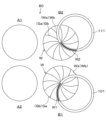
- FIG. 6 is an explanatory diagram showing grinding marks formed on both surfaces of a wafer in a comparative example
- FIG. 3 is an explanatory diagram showing grinding marks formed on both surfaces of a wafer in this embodiment
- FIG. 2 is a flow chart showing main steps of wafer processing; It is explanatory drawing which shows a mode that the 1st surface (2nd surface) of a wafer is ground with a grinding apparatus in other embodiment. It is a top view showing an outline of composition of a wafer processing system concerning other embodiments.
- a disk-shaped silicon piece cut out from a single crystal silicon ingot by a wire saw or the like is ground and flattened on both front and back surfaces. ing. Then, a silicon wafer (hereinafter sometimes referred to as "wafer”) is manufactured.
- a wafer processing system as a substrate processing system and a wafer processing method as a substrate processing method according to the present embodiment will be described below with reference to the drawings.
- elements having substantially the same functional configuration are denoted by the same reference numerals, thereby omitting redundant description.
- a wafer W as a substrate obtained by cutting an ingot is subjected to processing for improving in-plane thickness uniformity.
- the cut surfaces of the wafer W are referred to as a first surface Wa and a second surface Wb.
- the first surface Wa is the surface opposite to the second surface Wb.
- the first surface Wa and the second surface Wb may be collectively referred to as one surface of the wafer W. As shown in FIG.
- the wafer processing system 1 has a configuration in which a loading/unloading station 10 and a processing station 11 are integrally connected.
- a loading/unloading station 10 loads/unloads a cassette C capable of accommodating a plurality of wafers W, for example, to/from the outside.
- the processing station 11 includes various processing devices for performing desired processing on the wafer W.
- FIG. In the following description, a plurality of wafers W housed in the cassette C will be referred to as one lot.
- a cassette mounting table 20 is provided in the loading/unloading station 10 .
- a plurality of, for example, two cassettes C can be placed in a row on the cassette placing table 20 in the Y-axis direction.
- the number of cassettes C to be placed on the cassette placing table 20 is not limited to that of the present embodiment, and can be arbitrarily determined.
- the processing station 11 is provided with, for example, three processing blocks G1 to G3.
- the first processing block G1, the second processing block G2, and the third processing block G3 are arranged side by side in this order from the X-axis negative direction side (carrying in/out station 10 side) to the positive direction side.
- An etching device 30, a cleaning device 40, and a wafer transfer device 50 are provided in the first processing block G1.
- the etching apparatus 30 is provided in three stages in the vertical direction, for example, on the loading/unloading station 10 side of the first processing block G1.
- the cleaning device 40 is provided in three stages in the vertical direction, for example, on the positive direction side of the X-axis of the etching device 30 .
- the wafer transfer device 50 is arranged on the Y-axis positive side of the etching device 30 and the cleaning device 40 . Note that the number and arrangement of the etching device 30, the cleaning device 40, and the wafer transfer device 50 are not limited to this.
- the etching device 30 etches the ground first surface Wa or the ground second surface Wb.
- an etchant chemical solution
- HF, HNO 3 , H 3 PO 4 , TMAH, Choline, KOH, or the like is supplied to the first surface Wa or the ground second surface Wb.
- HF, HNO 3 , H 3 PO 4 , TMAH, Choline, KOH, or the like is used as the etchant.
- the cleaning device 40 cleans the ground first surface Wa or the ground second surface Wb.
- a brush is brought into contact with the first surface Wa or the second surface Wb to scrub clean the first surface Wa or the second surface Wb.
- a pressurized cleaning liquid may be used for cleaning the first surface Wa or the second surface Wb.
- the cleaning device 40 may be configured to be able to clean the first surface Wa and the second surface Wb at the same time when cleaning the wafer W. As shown in FIG.
- the wafer transfer device 50 has, for example, two transfer arms 51 that hold and transfer the wafer W.
- Each transport arm 51 is configured to be movable in the horizontal direction, the vertical direction, around the horizontal axis, and around the vertical axis.
- the wafer transfer device 50 is configured to transfer the wafer W to the cassette C of the cassette mounting table 20, the etching device 30, the cleaning device 40, which will be described later, the transition device 60, which will be described later, and the reversing device 61, which will be described later. ing.
- a transition device 60, a reversing device 61, and a wafer transfer device 70 are provided in the second processing block G2.
- the transition device 60 and the reversing device 61 are stacked in this order from the bottom in the vertical direction, for example.
- the wafer transfer device 70 is arranged on the Y-axis negative direction side of the transition device 60 and the reversing device 61 . Note that the number and arrangement of the transition device 60, the reversing device 61, and the wafer transfer device 70 are not limited to this.
- the transition device 60 temporarily places the wafer W in order to transfer the wafer W.
- the reversing device 61 reverses the first surface Wa and the second surface Wb of the wafer W in the vertical direction.
- the wafer transfer device 70 has, for example, two transfer arms 71 that hold and transfer the wafer W.
- Each transport arm 71 is configured to be movable in the horizontal direction, the vertical direction, around the horizontal axis, and around the vertical axis.
- the wafer transfer device 70 is configured to transfer the wafer W to the cleaning device 40, the transition device 60, the reversing device 61, and the grinding device 80, which will be described later.
- a grinding device 80 is provided in the third processing block G3. Note that the number and arrangement of the grinding devices 80 are not limited to this.
- the grinding device 80 has a rotary table 81 .
- the rotary table 81 is rotatable around a vertical center line 82 of rotation by a rotary mechanism (not shown).
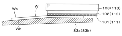
- Four chucks 83 are provided on the rotary table 81 as holding portions for holding the wafer W by suction.
- two first chucks 83a are chucks used for grinding the first surface Wa, and hold the second surface Wb by suction.
- These two first chucks 83a are arranged point-symmetrically with respect to the rotation center line 82 .
- the remaining two second chucks 83b are chucks used for grinding the second surface Wb, and hold the first surface Wa by suction.
- These two second chucks 83b are also arranged point-symmetrically across the rotation center line 82 . That is, the first chucks 83a and the second chucks 83b are alternately arranged in the circumferential direction.
- a porous chuck is used for the chuck 83.
- the surface of the chuck 83 that is, the holding surface of the wafer W, has a convex shape in which the central portion protrudes from the end portions when viewed from the side. It should be noted that although the protrusion at the central portion is minute, the protrusion at the central portion of the chuck 83 is shown enlarged in FIG. 2 for clarity of explanation.
- the chuck 83 is held by a chuck base 84.
- the chuck base 84 is provided with an inclination adjusting portion 85 for adjusting the relative inclination between the grinding wheels 101 and 111 provided in the respective grinding units 100 and 110 and the chuck 83, which will be described later.
- the tilt adjusting portion 85 has a fixed shaft 86 provided on the lower surface of the chuck base 84 and a plurality of, for example, two elevating shafts 87 . Each elevating shaft 87 is extendable and elevates the chuck base 84 .
- the chuck 83 and the chuck base are vertically moved up and down with one end (position corresponding to the fixed shaft 86) of the outer peripheral portion of the chuck base 84 by the lifting shaft 87. 84 can be tilted. Thereby, the relative inclination between the surfaces of the grinding wheels 101 and 111 and the surface of the chuck 83 provided in the grinding units 100 and 110 at the processing positions B1 and B2, which will be described later, can be adjusted.
- the configuration of the tilt adjusting section 85 is not limited to this, and can be arbitrarily selected as long as the relative angle (parallelism) of the surface of the chuck 83 to the surfaces of the grinding wheels 101 and 111 can be adjusted.
- the four chucks 83 are movable to transfer positions A1 to A2 and processing positions B1 to B2 by rotating the rotary table 81.
- Each of the four chucks 83 is configured to be rotatable about a vertical axis by a rotating mechanism (not shown).
- the first transfer position A1 is a position on the X-axis negative direction side and the Y-axis positive direction side of the rotary table 81, and the wafer W is transferred to and from the first chuck 83a when the wafer W is ground.
- the second transfer position A2 is a position on the X-axis negative direction side and the Y-axis negative direction side of the rotary table 81, and the wafer W is transferred to and from the second chuck 83b when the wafer W is ground.
- a thickness measuring unit 90 for measuring the thickness of the wafer W after grinding is provided at the delivery positions A1 and A2.
- the thickness measuring unit 90 measures the thickness of the wafer W at a plurality of points to measure the in-plane distribution of the thickness.
- the configuration of the thickness measuring unit 90 is arbitrary, but for example, it includes a non-contact sensor (not shown).
- the first machining position B1 is a position on the X-axis positive direction side and the Y-axis negative direction side of the rotary table 81, where the first grinding unit 100 as the first grinding section is arranged.
- the first grinding unit 100 grinds either the first surface Wa or the second surface Wb of the wafer W held by the first chuck 83a.
- the second machining position B2 is a position on the positive direction side of the X-axis and the positive direction side of the Y-axis of the rotary table 81, and the second grinding unit 110 as a second grinding section is arranged.
- the second grinding unit 110 grinds either the first surface Wa or the second surface Wb held by the second chuck 83b.
- the rotary table 81 transports and positions the wafer W held by the first chuck 83a to the first grinding unit 100, or transfers the wafer W held by the second chuck 83b to the second grinding unit 100. It functions as a transport section that transports and positions the wafer to the grinding unit 110 .
- the first grinding unit 100 includes a grinding wheel 102 having an annular grinding wheel 101 on its underside, a mount 103 supporting the grinding wheel 102, and a mount 103 for rotating the grinding wheel 102. It has a spindle 104 and a drive unit 105 containing, for example, a motor (not shown). Also, the first grinding unit 100 is configured to be movable in the vertical direction along the column 106 shown in FIG.
- the second grinding unit 110 has the same configuration as the first grinding unit 100. That is, the second grinding unit 110 has a grinding wheel 112 with an annular grinding wheel 111 , a mount 113 , a spindle 114 , a drive 115 and a post 116 .
- the wafer processing system 1 described above is provided with a controller 120 as shown in FIG.
- the control device 120 is, for example, a computer equipped with a CPU, memory, etc., and has a program storage unit (not shown).
- a program for controlling the processing of wafers W in wafer processing system 1 is stored in the program storage unit.
- the above program may be recorded in a computer-readable storage medium H and installed in the control device 120 from the storage medium H. Further, the storage medium H may be temporary or non-temporary.
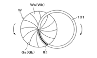
- the chucks 83a and 83b have a convex shape at the center of the wafer W holding surface. Therefore, when grinding the first surface Wa of the wafer W using the first grinding unit 100, the first surface Wa of the wafer W held by the first chuck 83a and the grinding wheel 101 are The first chuck 83a is tilted so as to be parallel to the surface. 4 and 5, part of the ring-shaped grinding wheel 101 contacts the wafer W as a first processing point R1. More specifically, the ring-shaped grinding wheel 101 and the wafer W are in contact with each other from the center to the outer peripheral edge in an arcuate manner. The entire surface Wa of 1 is ground. The same is true when grinding the second surface Wb of the wafer W using the first grinding unit 100 .
- the first surface Wa when the first surface Wa is ground using the first grinding unit 100, the first surface Wa has a first saw mark, which is a so-called saw mark, which is curved and extends from the center toward the outer periphery. of grinding marks Ga are formed.
- the second surface Wb when the second surface Wb is ground using the first grinding unit 100, the second surface Wb has a second grinding mark Gb that curves and extends from the central portion toward the outer peripheral portion. It is formed.
- Each of the first grinding mark Ga and the second grinding mark Gb has a continuous curved convex portion clockwise, and in the following description, the curved direction may be referred to as "clockwise".
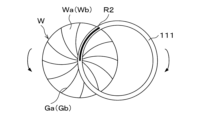
- the second chuck 83b is tilted so that the surface of the grindstone 111 is parallel. Further, as indicated by the thick line in FIG. 6, a portion of the ring-shaped grinding wheel 111 contacts the wafer W as a second processing point R2. More specifically, the ring-shaped grinding wheel 111 and the wafer W are in contact with each other in an arc from the center to the outer peripheral edge. The entire surface Wa of 1 is ground. The same applies when the second surface Wb of the wafer W is ground using the second grinding unit 110 .
- the first surface Wa when the first surface Wa is ground using the second grinding unit 110, the first surface Wa has a first grinding mark Ga that curves and extends from the center toward the outer periphery. It is formed. Also, when the second surface Wb is ground using the second grinding unit 110, the second surface Wb has a second grinding mark Gb that curves and extends from the central portion toward the outer peripheral portion. It is formed.
- Each of the first grinding mark Ga and the second grinding mark Gb has a curved convex portion continuing counterclockwise, and in the following description, the curved direction may be referred to as "counterclockwise".
- the first grinding unit 100 is used.
- the position of the first machining point R1 in the case of using the second grinding unit 110 is different from the position of the second machining point R2 in the case of using the second grinding unit 110 . Therefore, the curved direction of the grinding marks Ga and Gb when the first grinding unit 100 is used and the curved direction of the grinding marks Ga and Gb when the second grinding unit 110 is used are the same on the wafer W. On the surface it is the opposite.
- the grinding marks Ga and Gb overlap.
- the first surface Wa is ground by the first grinding unit 100 to form clockwise first grinding marks Ga.
- the second surface Wb is ground by the second grinding unit 110 to form a counterclockwise second ground mark Gb.
- the grinding marks Ga and Gb overlap when viewed from one side. In such a case, grinding damage may increase.
- the surfaces Wa and Wb of one wafer W are ground by the same grinding units 100 and 110, respectively.
- the first surface Wa is ground by the first grinding unit 100 to form clockwise first grinding marks Ga.
- the second surface Wb is ground by the first grinding unit 100 to form a clockwise second grinding mark Gb.
- the curved directions of the grinding marks Ga and Gb are made the same as described above, the grinding marks Ga and Gb on the wafer W do not cross and overlap each other as shown in FIG. 9(c). In such a case, grinding damage can be suppressed as compared with the case where the grinding marks Ga and Gb overlap.
- the surfaces Wa and Wb of one wafer W are respectively ground by the second grinding unit 110, the grinding marks Ga and Gb do not overlap when viewed from the one surface, and the same effect can be obtained. can be done.
- the present inventors found that there is a correlation between the direction of curvature of the grinding marks Ga and Gb and the grinding damage, and that the grinding damage can be suppressed by appropriately controlling the directions of the grinding marks Ga and Gb. I found
- wafer processing performed using the wafer processing system 1 configured as described above will be described.
- a desired process is performed on a wafer W that is cut out from an ingot by a wire saw or the like and lapped.
- a cassette C containing a plurality of wafers W is mounted on the cassette mounting table 20 of the loading/unloading station 10 .
- the wafers W are stored in the cassette C with the first surface Wa facing upward and the second surface Wb facing downward.
- the wafer W in the cassette C is taken out by the wafer transfer device 50 and transferred to the transition device 60 .
- the wafer W is transferred to the grinding device 80 by the wafer transfer device 70 and transferred to the first chuck 83a at the first transfer position A1.
- the second surface Wb of the wafer W is held by suction on the first chuck 83a.
- the rotary table 81 is rotated to move the wafer W to the first processing position B1. Then, the first surface Wa of the wafer W is ground by the first grinding unit 100 (step S1 in FIG. 10). At this time, as shown in FIG. 9A, a clockwise first grinding mark Ga is formed on the first surface Wa.
- the rotary table 81 is rotated to move the wafer W to the first delivery position A1.
- the wafer W is transferred to the cleaning device 40 by the wafer transfer device 70 .
- the cleaning device 40 the first surface Wa of the wafer W is cleaned (step S2 in FIG. 10).
- the wafer W is transferred to the reversing device 61 by the wafer transfer device 70 .
- the reversing device 61 vertically reverses the first surface Wa and the second surface Wb of the wafer W (step S3 in FIG. 10). That is, the wafer W is turned over so that the second surface Wb faces upward and the first surface Wa faces downward.
- the wafer W is transferred to the grinding device 80 by the wafer transfer device 70 and transferred to the first chuck 83a at the first transfer position A1.
- the first surface Wa of the wafer W is held by suction on the first chuck 83a.
- the rotary table 81 is rotated to move the wafer W to the first processing position B1. Then, the second surface Wb of the wafer W is ground by the first grinding unit 100 (step S4 in FIG. 10). At this time, as shown in FIG. 9B, a clockwise second grinding mark Gb is formed on the second surface Wb. Then, since the curved directions of the grinding marks Ga and Gb are the same, the grinding marks Ga and Gb do not overlap when viewed from one side as shown in FIG. 9(c).
- the rotary table 81 is rotated to move the wafer W to the second delivery position A2.
- the wafer W is transferred to the cleaning device 40 by the wafer transfer device 70 .
- second surface Wb of wafer W is cleaned (step S5 in FIG. 10).
- the wafer W is transferred to the reversing device 61 by the wafer transfer device 50 .
- the reversing device 61 vertically reverses the first surface Wa and the second surface Wb of the wafer W (step S6 in FIG. 10). That is, the wafer W is turned over so that the first surface Wa faces upward and the second surface Wb faces downward.
- the wafer W is transferred to the etching device 30 by the wafer transfer device 50 .
- the first surface Wa of the wafer W is etched with an etchant (step S7 in FIG. 10). As a result, grinding debris, grinding damage, and the like remaining on the first surface Wa are removed.
- the wafer W is transferred to the reversing device 61 by the wafer transfer device 50 .
- the reversing device 61 vertically reverses the first surface Wa and the second surface Wb of the wafer W (step S8 in FIG. 10). That is, the wafer W is turned over so that the second surface Wb faces upward and the first surface Wa faces downward.
- the wafer W is transferred to the etching device 30 by the wafer transfer device 50 .
- the second surface Wb of the wafer W is etched with an etchant (step S9 in FIG. 10). As a result, grinding debris, grinding damage, etc. remaining on the second surface Wb are removed.
- the wafer W that has undergone all the processes is transferred to the cassette C on the cassette mounting table 20 by the wafer transfer device 50 .
- a series of wafer processing in the wafer processing system 1 is completed. Wafers W that have undergone desired processing in wafer processing system 1 may be subjected to polishing outside wafer processing system 1 .
- the grinding marks Ga and Gb on the wafer W can be formed so as not to overlap each other. . Therefore, grinding damage can be suppressed. As a result, the conventional flattening and smoothing processes for removing grinding damage are not necessary or can be reduced, so it is possible to improve productivity and reduce man-hours in wafer manufacturing. .
- the plurality of wafers W housed in the same cassette C may be alternately transferred to the first grinding unit 100 and the second grinding unit 110 one by one.
- the second grinding unit 110 is not used until the wafers W in the next lot are ground. That is, the first grinding unit 100 and the second grinding unit 110 cannot be used in parallel, resulting in poor wafer processing efficiency.
- the control device 120 controls the transfer of the wafers W in the grinding device 80, and alternately distributes the wafers W in the same cassette C to the first grinding unit 100 and the second grinding unit 110 for transfer.
- the first grinding unit 100 and the second grinding unit 110 can be used in parallel, the wafers W can be processed efficiently, and the throughput of the wafers W can be improved.
- the grinding device 80 has a first grinding unit 100 (grinding wheel 102) and a second grinding unit 100 (grinding wheel 102) so that the same grinding mark is formed by the first machining point R1 and the second machining point R2. of the grinding unit 110 (grinding wheel 112 ) is positioned relative to the chuck 83 .
- the direction of curvature of the grinding marks Ga and Gb when the first grinding unit 100 is used is the same as the direction of curvature of the grinding marks Ga and Gb when the second grinding unit 110 is used.
- the clockwise first grinding marks Ga or the second clockwise grinding marks Gb are formed. It is formed. Further, when the first surface Wa or the second surface Wb of the wafer W is ground using the second grinding unit 110, the clockwise first grinding marks Ga or the second clockwise grinding marks Gb are left respectively. It is formed.
- one wafer W is moved to the first processing position B1 in step S1, and the first surface Wa of the wafer W is ground by the first grinding unit 100.
- a clockwise first grinding mark Ga is formed on the first surface Wa.
- step S3 the wafer W is moved to the second processing position B2, and the second surface Wb of the wafer W is ground by the second grinding unit 110. Then, a clockwise second grinding mark Gb is formed on the second surface Wb.
- the control device 120 controls the rotary table 81, which is the transport section, the first grinding unit 100 and the second grinding unit 110.
- the grinding marks Ga and Gb do not cross and overlap each other. As a result, grinding damage can be suppressed.
- the grinding marks Ga and Gb when the first grinding unit 100 is used and the grinding marks Ga and Gb when the second grinding unit 110 is used may be left-handed. That is, the first grinding unit 100 (grinding wheel 102) and the second grinding unit 110 (grinding wheel 112) are arranged with respect to the chuck 83 so that the curved directions of the grinding marks Ga and Gb are in one direction. With the grinding device 80, it is possible to enjoy the same effects as described above. A plurality of wafers W accommodated in the same cassette C can be continuously processed by first transferring them to the first grinding unit 100 and then transferring them to the second grinding unit 110. processing throughput can be improved.
- the wafer processing system 1 has a plurality of, for example, two grinding devices 200 and 210 instead of the grinding device 80 of the above embodiment.
- the grinding devices 200 and 210 are arranged side by side in this order from the X-axis negative direction side to the positive direction side.
- the wafer transfer device 70 is configured to move along a rail 72 extending in the X-axis direction and transfer the wafer W to the grinding devices 200 and 210 .
- the first grinding device 200 has a chuck 201 that sucks and holds the wafer W, and a grinding unit 202 .
- the chuck 201 is configured to be movable between a delivery position and a processing position by a moving mechanism (not shown). At the transfer position, the wafer W is transferred to and from the chuck 201 when the wafer W is ground.
- a grinding unit 202 is arranged at the processing position.
- the grinding unit 202 has the same configuration as the grinding units 100 , 110 , and 130 of the above embodiments, and grinds the first surface Wa of the wafer W held by the chuck 201 .
- the grinding unit 202 is arranged with respect to the chuck 201 so that the clockwise first grinding mark Ga is formed on the first surface Wa of the wafer W. As shown in FIG.
- the second grinding device 210 has the same configuration as the first grinding device 200 and has a chuck 211 and a grinding unit 212 .
- Grinding unit 212 grinds second surface Wb of wafer W held by chuck 211 .
- the grinding unit 212 is arranged with respect to the chuck 211 so that the clockwise second grinding marks Gb are formed on the second surface Wb of the wafer W. As shown in FIG.
- step S1 the first surface Wa of one wafer W is ground by the first grinding device 200, and a clockwise first grinding mark Ga is formed on the first surface Wa.
- step S3 the second surface Wb of the same wafer W is ground by the second grinding device 210 in step S3. Then, a clockwise second grinding mark Gb is formed on the second surface Wb.
- the grinding marks Ga and Gb do not cross and overlap each other. As a result, grinding damage can be suppressed.
- grinding marks are formed in advance on the wafer W by a previous process.
- the conveyance may be controlled so that opposite grinding marks are formed on the same surface.
- an imaging unit (not shown) for imaging one side of the wafer W may be provided inside the second grinding device 210, and the grinding unit 212 may be set according to the imaged first grinding marks Ga. good.
- control is performed so that the first grinding marks Ga formed on the first surface Wa of the wafer W and the second grinding marks Gb formed on the second surface Wb do not overlap.
- the disclosed method can also be applied when one side of the wafer W is ground in a plurality of stages. For example, in single-sided grinding consisting of two stages, in the first stage of grinding of the first surface Wa, a rightward first grinding mark Ga is formed, and in the second stage of grinding of the first surface Wa, the first leftward grinding mark Ga is formed. Control is performed to form grinding marks Ga. Then, on the first surface Wa, the grinding marks Ga in the first stage and the second stage do not overlap, and grinding damage can be suppressed.
- the first grinding marks Ga are formed in the direction opposite to the curved direction. , to the grinding unit 212 of the second grinding device 210 .
- the grinding damage is minimized according to the curved direction of the grinding marks Ga and Gb formed in the first-stage double-sided grinding in the first-stage grinding device.
- the curved directions of the grinding traces Ga and Gb formed by the second-stage double-sided grinding in the grinding device in the second stage are set.
- the grinding marks Ga and Gb formed in the first stage of double-sided grinding do not overlap, the grinding marks Ga and Gb in the first stage are crossed and the grinding formed in the second stage of double-sided grinding
- the traces Ga and Gb should not cross and overlap each other.
- the grinding marks Ga and Gb formed in the first stage of double-sided grinding overlap the grinding marks Ga or Gb on one side are crossed, and the grinding marks formed in the second stage of double-sided grinding are crossed. Traces Ga and Gb overlap.
- the first surface Wa and the second surface Wb may have different contribution rates to grinding damage.
- the surface that contributes less to the grinding damage is the first surface Wa, on the first surface Wa
- the first grinding traces Ga formed by are superimposed on each other.
- the surface that contributes greatly to the grinding damage is the second surface Wb, on the two surfaces Wb
- the second grinding marks Gb formed in the first stage of grinding and the second grinding marks Gb are formed in the second stage of grinding.
- the second grinding marks Gb to be cut are prevented from crossing and overlapping each other.
- Wafer Processing System 80 Grinding Device 120 Control Device Ga First Grinding Mark Gb Second Grinding Mark W Wafer Wa First Surface Wb Second Surface
Abstract
Provided is a substrate processing method for processing a substrate, comprising grinding a first surface of the substrate, and, after the first surface has been ground, grinding a second surface of the substrate opposite the first surface. During the grinding of the first surface, a first grinding mark is formed that curves and extends from a central portion of the first surface toward an outer periphery. During the grinding of the second surface, a second grinding mark is formed curving and extending from a central portion of the second surface toward the outer periphery. The curving direction of the first grinding mark and the curving direction of the second grinding mark are opposite from each other in a transparent view from one surface.
Description
本開示は、基板処理方法及び基板処理システムに関する。
The present disclosure relates to a substrate processing method and a substrate processing system.
特許文献1には、基板の両面を研削する基板処理システムが開示されている。基板処理システムは、基板の第1主表面を上に向けて基板を下方から保持すると共に、基板の第1主表面を研削する第1主表面研削装置と、基板の第2主表面を上に向けて基板の研削された第1主表面を下方から保持すると共に、基板の第2主表面を研削する第2主表面研削装置と、を備える。
Patent Document 1 discloses a substrate processing system that grinds both sides of a substrate. The substrate processing system holds the substrate from below with the first main surface of the substrate facing upward, and includes a first main surface grinding device for grinding the first main surface of the substrate, and a second main surface of the substrate facing upward. a second main surface grinding device that holds the ground first main surface of the substrate toward the substrate from below and grinds the second main surface of the substrate.
本開示にかかる技術は、基板の両面を研削した後の、当該基板の研削ダメージを抑制する。
The technology according to the present disclosure suppresses grinding damage of the substrate after grinding both sides of the substrate.
本開示の一態様は、基板を処理する基板処理方法であって、前記基板の第1の面を研削することと、前記第1の面を研削した後、前記基板の前記第1の面と反対側の第2の面を研削することと、を含み、前記第1の面を研削する際、当該第1の面の中心部から外周部に向けて湾曲して延伸する第1の研削痕が形成され、前記第2の面を研削する際、当該第2の面の中心部から外周部に向けて湾曲して延伸する第2の研削痕が形成され、前記第1の研削痕の湾曲方向と前記第2の研削痕の湾曲方向は一の面から透視した際に反対になる。
One aspect of the present disclosure is a substrate processing method for processing a substrate, comprising: grinding a first surface of the substrate; Grinding a second surface on the opposite side, wherein when the first surface is ground, a first grinding mark that curves and extends from the center of the first surface toward the outer periphery. is formed, and when grinding the second surface, a second grinding mark that curves and extends from the center of the second surface toward the outer peripheral portion is formed, and the curvature of the first grinding mark The direction and the curving direction of the second grinding marks are opposite when seen through from one surface.
本開示によれば、基板の両面を研削した後の、当該基板の研削ダメージを抑制することができる。
According to the present disclosure, it is possible to suppress grinding damage of the substrate after grinding both sides of the substrate.
半導体デバイスの製造工程では、例えば上述した特許文献1に開示されたように、単結晶シリコンインゴットからワイヤーソー等により切り出された円盤状シリコン片の表裏両面を、研削し平坦化することが行われている。そして、シリコンウェハ(以下、「ウェハ」という場合がある。)が製造される。
In the manufacturing process of a semiconductor device, for example, as disclosed in the above-mentioned Patent Document 1, a disk-shaped silicon piece cut out from a single crystal silicon ingot by a wire saw or the like is ground and flattened on both front and back surfaces. ing. Then, a silicon wafer (hereinafter sometimes referred to as "wafer") is manufactured.
ここで、ウェハ製造の生産性向上や工数削減のために、研削加工における研削ダメージをできるだけ抑制する必要がある。しかしながら、従来、この研削ダメージを抑制することまでは考慮されていない。
Here, in order to improve the productivity of wafer manufacturing and reduce man-hours, it is necessary to suppress grinding damage in the grinding process as much as possible. Conventionally, however, no consideration has been given to suppressing this grinding damage.
本開示にかかる技術は、基板の両面研削時の、当該基板の研削ダメージを抑制する。以下、本実施形態にかかる基板処理システムとしてのウェハ処理システム、及び基板処理方法としてのウェハ処理方法について、図面を参照しながら説明する。なお、本明細書及び図面において、実質的に同一の機能構成を有する要素においては、同一の符号を付することにより重複説明を省略する。
The technology according to the present disclosure suppresses grinding damage of the substrate during double-sided grinding of the substrate. A wafer processing system as a substrate processing system and a wafer processing method as a substrate processing method according to the present embodiment will be described below with reference to the drawings. In the present specification and drawings, elements having substantially the same functional configuration are denoted by the same reference numerals, thereby omitting redundant description.
本実施形態にかかるウェハ処理システム1では、インゴットから切り出して得られた基板としてのウェハWに対し、厚みの面内均一性を向上させるための処理を行う。以下、ウェハWの切り出し面を第1の面Waと第2の面Wbという。第1の面Waは第2の面Wbの反対側の面である。また、第1の面Waと第2の面Wbを総称してウェハWの片面という場合がある。
In the wafer processing system 1 according to the present embodiment, a wafer W as a substrate obtained by cutting an ingot is subjected to processing for improving in-plane thickness uniformity. Hereinafter, the cut surfaces of the wafer W are referred to as a first surface Wa and a second surface Wb. The first surface Wa is the surface opposite to the second surface Wb. Also, the first surface Wa and the second surface Wb may be collectively referred to as one surface of the wafer W. As shown in FIG.
図1に示すようにウェハ処理システム1は、搬入出ステーション10と処理ステーション11を一体に接続した構成を有している。搬入出ステーション10は、例えば外部との間で複数のウェハWを収容可能なカセットCが搬入出される。処理ステーション11は、ウェハWに対して所望の処理を施す各種処理装置を備えている。なお、以下の説明において、カセットCに収容された複数のウェハWを1ロットという。
As shown in FIG. 1, the wafer processing system 1 has a configuration in which a loading/unloading station 10 and a processing station 11 are integrally connected. A loading/unloading station 10 loads/unloads a cassette C capable of accommodating a plurality of wafers W, for example, to/from the outside. The processing station 11 includes various processing devices for performing desired processing on the wafer W. FIG. In the following description, a plurality of wafers W housed in the cassette C will be referred to as one lot.
搬入出ステーション10には、カセット載置台20が設けられている。図示の例では、カセット載置台20には、複数、例えば2つのカセットCをY軸方向に一列に載置自在になっている。なお、カセット載置台20に載置されるカセットCの個数は、本実施形態に限定されず、任意に決定することができる。
A cassette mounting table 20 is provided in the loading/unloading station 10 . In the illustrated example, a plurality of, for example, two cassettes C can be placed in a row on the cassette placing table 20 in the Y-axis direction. Note that the number of cassettes C to be placed on the cassette placing table 20 is not limited to that of the present embodiment, and can be arbitrarily determined.
処理ステーション11には、例えば3つの処理ブロックG1~G3が設けられている。第1の処理ブロックG1、第2の処理ブロックG2及び第3の処理ブロックG3は、X軸負方向側(搬入出ステーション10側)から正方向側にこの順で並べて配置されている。
The processing station 11 is provided with, for example, three processing blocks G1 to G3. The first processing block G1, the second processing block G2, and the third processing block G3 are arranged side by side in this order from the X-axis negative direction side (carrying in/out station 10 side) to the positive direction side.
第1の処理ブロックG1には、エッチング装置30、洗浄装置40、及びウェハ搬送装置50が設けられている。エッチング装置30は、第1の処理ブロックG1の搬入出ステーション10側において、例えば鉛直方向に3段に設けられている。洗浄装置40は、エッチング装置30のX軸正方向側において、例えば鉛直方向に3段に設けられている。ウェハ搬送装置50は、エッチング装置30及び洗浄装置40のY軸正方向側に配置されている。なお、エッチング装置30、洗浄装置40、及びウェハ搬送装置50の数や配置はこれに限定されない。
An etching device 30, a cleaning device 40, and a wafer transfer device 50 are provided in the first processing block G1. The etching apparatus 30 is provided in three stages in the vertical direction, for example, on the loading/unloading station 10 side of the first processing block G1. The cleaning device 40 is provided in three stages in the vertical direction, for example, on the positive direction side of the X-axis of the etching device 30 . The wafer transfer device 50 is arranged on the Y-axis positive side of the etching device 30 and the cleaning device 40 . Note that the number and arrangement of the etching device 30, the cleaning device 40, and the wafer transfer device 50 are not limited to this.
エッチング装置30は、研削後の第1の面Wa又は研削後の第2の面Wbをエッチングする。例えば第1の面Wa又は研削後の第2の面Wbに対してエッチング液(薬液)を供給し、当該第1の面Wa又は研削後の第2の面Wbをウェットエッチングする。エッチング液には、例えばHF、HNO3、H3PO4、TMAH、Choline、KOH等が用いられる。
The etching device 30 etches the ground first surface Wa or the ground second surface Wb. For example, an etchant (chemical solution) is supplied to the first surface Wa or the ground second surface Wb to wet-etch the first surface Wa or the ground second surface Wb. For example, HF, HNO 3 , H 3 PO 4 , TMAH, Choline, KOH, or the like is used as the etchant.
洗浄装置40は、研削後の第1の面Wa又は研削後の第2の面Wbを洗浄する。例えば第1の面Wa又は第2の面Wbにブラシを当接させて、当該第1の面Wa又は第2の面Wbをスクラブ洗浄する。なお、第1の面Wa又は第2の面Wbの洗浄には、加圧された洗浄液を用いてもよい。また、洗浄装置40は、ウェハWを洗浄する際、第1の面Waと第2の面Wbを同時に洗浄可能に構成されていてもよい。
The cleaning device 40 cleans the ground first surface Wa or the ground second surface Wb. For example, a brush is brought into contact with the first surface Wa or the second surface Wb to scrub clean the first surface Wa or the second surface Wb. A pressurized cleaning liquid may be used for cleaning the first surface Wa or the second surface Wb. Further, the cleaning device 40 may be configured to be able to clean the first surface Wa and the second surface Wb at the same time when cleaning the wafer W. As shown in FIG.
ウェハ搬送装置50は、ウェハWを保持して搬送する、例えば2つの搬送アーム51を有している。各搬送アーム51は、水平方向、鉛直方向、水平軸回り及び鉛直軸周りに移動自在に構成されている。そして、ウェハ搬送装置50は、カセット載置台20のカセットC、エッチング装置30、後述する洗浄装置40、後述するトランジション装置60、及び後述する反転装置61に対して、ウェハWを搬送可能に構成されている。
The wafer transfer device 50 has, for example, two transfer arms 51 that hold and transfer the wafer W. Each transport arm 51 is configured to be movable in the horizontal direction, the vertical direction, around the horizontal axis, and around the vertical axis. The wafer transfer device 50 is configured to transfer the wafer W to the cassette C of the cassette mounting table 20, the etching device 30, the cleaning device 40, which will be described later, the transition device 60, which will be described later, and the reversing device 61, which will be described later. ing.
第2の処理ブロックG2には、トランジション装置60、反転装置61、及びウェハ搬送装置70が設けられている。トランジション装置60と反転装置61は、例えば鉛直方向に下段からこの順で積層して設けられている。ウェハ搬送装置70は、トランジション装置60及び反転装置61のY軸負方向側に配置されている。なお、トランジション装置60、反転装置61、及びウェハ搬送装置70の数や配置はこれに限定されない。
A transition device 60, a reversing device 61, and a wafer transfer device 70 are provided in the second processing block G2. The transition device 60 and the reversing device 61 are stacked in this order from the bottom in the vertical direction, for example. The wafer transfer device 70 is arranged on the Y-axis negative direction side of the transition device 60 and the reversing device 61 . Note that the number and arrangement of the transition device 60, the reversing device 61, and the wafer transfer device 70 are not limited to this.
トランジション装置60は、ウェハWを受け渡すために、当該ウェハWを一時的に載置する。反転装置61は、ウェハWの第1の面Waと第2の面Wbを上下方向に反転させる。
The transition device 60 temporarily places the wafer W in order to transfer the wafer W. The reversing device 61 reverses the first surface Wa and the second surface Wb of the wafer W in the vertical direction.
ウェハ搬送装置70は、ウェハWを保持して搬送する、例えば2つの搬送アーム71を有している。各搬送アーム71は、水平方向、鉛直方向、水平軸回り及び鉛直軸周りに移動自在に構成されている。そして、ウェハ搬送装置70は、洗浄装置40、トランジション装置60、反転装置61、及び後述する研削装置80に対して、ウェハWを搬送可能に構成されている。
The wafer transfer device 70 has, for example, two transfer arms 71 that hold and transfer the wafer W. Each transport arm 71 is configured to be movable in the horizontal direction, the vertical direction, around the horizontal axis, and around the vertical axis. The wafer transfer device 70 is configured to transfer the wafer W to the cleaning device 40, the transition device 60, the reversing device 61, and the grinding device 80, which will be described later.
第3の処理ブロックG3には、研削装置80が設けられている。なお、研削装置80の数や配置はこれに限定されない。
A grinding device 80 is provided in the third processing block G3. Note that the number and arrangement of the grinding devices 80 are not limited to this.
研削装置80は、回転テーブル81を有している。回転テーブル81は、回転機構(図示せず)によって、鉛直な回転中心線82を中心に回転自在に構成されている。回転テーブル81上には、ウェハWを吸着保持する、保持部としてのチャック83が4つ設けられている。4つのチャック83のうち、2つの第1のチャック83aは第1の面Waの研削に用いられるチャックであり、第2の面Wbを吸着保持する。これら2つの第1のチャック83aは、回転中心線82を挟んで点対称の位置に配置されている。残りの2つの第2のチャック83bは第2の面Wbの研削に用いられるチャックであり、第1の面Waを吸着保持する。これら2つの第2のチャック83bも、回転中心線82を挟んで点対称の位置に配置されている。すなわち、第1のチャック83aと第2のチャック83bは、周方向に交互に配置されている。
The grinding device 80 has a rotary table 81 . The rotary table 81 is rotatable around a vertical center line 82 of rotation by a rotary mechanism (not shown). Four chucks 83 are provided on the rotary table 81 as holding portions for holding the wafer W by suction. Of the four chucks 83, two first chucks 83a are chucks used for grinding the first surface Wa, and hold the second surface Wb by suction. These two first chucks 83a are arranged point-symmetrically with respect to the rotation center line 82 . The remaining two second chucks 83b are chucks used for grinding the second surface Wb, and hold the first surface Wa by suction. These two second chucks 83b are also arranged point-symmetrically across the rotation center line 82 . That is, the first chucks 83a and the second chucks 83b are alternately arranged in the circumferential direction.
チャック83には例えばポーラスチャックが用いられる。チャック83の表面、すなわちウェハWの保持面は、側面視において中央部が端部に比べて突出した凸形状を有している。なお、この中央部の突出は微小であるが、図2においては、説明の明瞭化のためチャック83の中央部の突出を大きく図示している。
For the chuck 83, for example, a porous chuck is used. The surface of the chuck 83, that is, the holding surface of the wafer W, has a convex shape in which the central portion protrudes from the end portions when viewed from the side. It should be noted that although the protrusion at the central portion is minute, the protrusion at the central portion of the chuck 83 is shown enlarged in FIG. 2 for clarity of explanation.
図2に示すように、チャック83はチャックベース84に保持されている。チャックベース84には、後述する各研削ユニット100、110が備える研削砥石101、111とチャック83の相対的な傾きを調整する傾き調整部85が設けられている。傾き調整部85は、チャックベース84の下面に設けられた固定軸86と複数、例えば2本の昇降軸87を有している。各昇降軸87は伸縮自在に構成され、チャックベース84を昇降させる。この傾き調整部85によって、チャックベース84の外周部の一端部(固定軸86に対応する位置)を基点に、他端部を昇降軸87によって鉛直方向に昇降させることで、チャック83及びチャックベース84を傾斜させることができる。そしてこれにより、後述する加工位置B1~B2の各研削ユニット100、110が備える研削砥石101、111の表面とチャック83の表面との相対的な傾きを調整することができる。
As shown in FIG. 2, the chuck 83 is held by a chuck base 84. The chuck base 84 is provided with an inclination adjusting portion 85 for adjusting the relative inclination between the grinding wheels 101 and 111 provided in the respective grinding units 100 and 110 and the chuck 83, which will be described later. The tilt adjusting portion 85 has a fixed shaft 86 provided on the lower surface of the chuck base 84 and a plurality of, for example, two elevating shafts 87 . Each elevating shaft 87 is extendable and elevates the chuck base 84 . With this inclination adjustment part 85, the chuck 83 and the chuck base are vertically moved up and down with one end (position corresponding to the fixed shaft 86) of the outer peripheral portion of the chuck base 84 by the lifting shaft 87. 84 can be tilted. Thereby, the relative inclination between the surfaces of the grinding wheels 101 and 111 and the surface of the chuck 83 provided in the grinding units 100 and 110 at the processing positions B1 and B2, which will be described later, can be adjusted.
なお、傾き調整部85の構成はこれに限定されず、研削砥石101、111の表面に対するチャック83の表面の相対的な角度(平行度)を調整することができれば、任意に選択できる。
The configuration of the tilt adjusting section 85 is not limited to this, and can be arbitrarily selected as long as the relative angle (parallelism) of the surface of the chuck 83 to the surfaces of the grinding wheels 101 and 111 can be adjusted.
図1に示すように4つのチャック83は、回転テーブル81が回転することにより、受渡位置A1~A2及び加工位置B1~B2に移動可能になっている。また、4つのチャック83はそれぞれ、回転機構(図示せず)によって鉛直軸回りに回転可能に構成されている。
As shown in FIG. 1, the four chucks 83 are movable to transfer positions A1 to A2 and processing positions B1 to B2 by rotating the rotary table 81. Each of the four chucks 83 is configured to be rotatable about a vertical axis by a rotating mechanism (not shown).
第1の受渡位置A1は回転テーブル81のX軸負方向側且つY軸正方向側の位置であり、ウェハWを研削する際に第1のチャック83aとの間でウェハWの受け渡しが行われる。第2の受渡位置A2は回転テーブル81のX軸負方向側且つY軸負方向側の位置であり、ウェハWを研削する際に第2のチャック83bとの間でウェハWの受け渡しが行われる。受渡位置A1、A2には、研削後のウェハWの厚みを測定する厚み測定部90が設けられている。厚み測定部90は、ウェハWの厚みを複数点で測定し、厚みの面内分布を測定する。厚み測定部90の構成は任意であるが、例えば非接触式のセンサ(図示せず)を備えている。
The first transfer position A1 is a position on the X-axis negative direction side and the Y-axis positive direction side of the rotary table 81, and the wafer W is transferred to and from the first chuck 83a when the wafer W is ground. . The second transfer position A2 is a position on the X-axis negative direction side and the Y-axis negative direction side of the rotary table 81, and the wafer W is transferred to and from the second chuck 83b when the wafer W is ground. . A thickness measuring unit 90 for measuring the thickness of the wafer W after grinding is provided at the delivery positions A1 and A2. The thickness measuring unit 90 measures the thickness of the wafer W at a plurality of points to measure the in-plane distribution of the thickness. The configuration of the thickness measuring unit 90 is arbitrary, but for example, it includes a non-contact sensor (not shown).
第1の加工位置B1は回転テーブル81のX軸正方向側且つY軸負方向側の位置であり、第1の研削部としての第1の研削ユニット100が配置される。第1の研削ユニット100は、第1のチャック83aに保持されたウェハWの第1の面Wa又は第2の面Wbのいずれか片面を研削する。第2の加工位置B2は回転テーブル81のX軸正方向側且つY軸正方向側の位置であり、第2の研削部としての第2の研削ユニット110が配置される。第2の研削ユニット110は、第2のチャック83bに保持された第1の面Wa又は第2の面Wbのいずれか片面を研削する。
The first machining position B1 is a position on the X-axis positive direction side and the Y-axis negative direction side of the rotary table 81, where the first grinding unit 100 as the first grinding section is arranged. The first grinding unit 100 grinds either the first surface Wa or the second surface Wb of the wafer W held by the first chuck 83a. The second machining position B2 is a position on the positive direction side of the X-axis and the positive direction side of the Y-axis of the rotary table 81, and the second grinding unit 110 as a second grinding section is arranged. The second grinding unit 110 grinds either the first surface Wa or the second surface Wb held by the second chuck 83b.
なお、本実施形態において回転テーブル81は、第1のチャック83aに保持されたウェハWを第1の研削ユニット100に搬送して位置づけ、又は第2のチャック83bに保持されたウェハWを第2の研削ユニット110に搬送して位置づける搬送部として機能する。
In this embodiment, the rotary table 81 transports and positions the wafer W held by the first chuck 83a to the first grinding unit 100, or transfers the wafer W held by the second chuck 83b to the second grinding unit 100. It functions as a transport section that transports and positions the wafer to the grinding unit 110 .
図2に示すように、第1の研削ユニット100は、下面に環状の研削砥石101を備える研削ホイール102と、研削ホイール102を支持するマウント103と、マウント103を介して研削ホイール102を回転させるスピンドル104と、例えばモータ(図示せず)を内蔵する駆動部105とを有している。また第1の研削ユニット100は、図1に示す支柱106に沿って鉛直方向に移動可能に構成されている。
As shown in FIG. 2, the first grinding unit 100 includes a grinding wheel 102 having an annular grinding wheel 101 on its underside, a mount 103 supporting the grinding wheel 102, and a mount 103 for rotating the grinding wheel 102. It has a spindle 104 and a drive unit 105 containing, for example, a motor (not shown). Also, the first grinding unit 100 is configured to be movable in the vertical direction along the column 106 shown in FIG.
第2の研削ユニット110は、第1の研削ユニット100と同様の構成を有している。すなわち、第2の研削ユニット110は、環状の研削砥石111を備える研削ホイール112、マウント113、スピンドル114、駆動部115、及び支柱116を有している。
The second grinding unit 110 has the same configuration as the first grinding unit 100. That is, the second grinding unit 110 has a grinding wheel 112 with an annular grinding wheel 111 , a mount 113 , a spindle 114 , a drive 115 and a post 116 .
以上のウェハ処理システム1には、図1に示すように制御装置120が設けられている。制御装置120は、例えばCPUやメモリ等を備えたコンピュータであり、プログラム格納部(図示せず)を有している。プログラム格納部には、ウェハ処理システム1におけるウェハWの処理を制御するプログラムが格納されている。なお、上記プログラムは、コンピュータに読み取り可能な記憶媒体Hに記録されていたものであって、当該記憶媒体Hから制御装置120にインストールされたものであってもよい。また、上記記憶媒体Hは、一時的なものであっても非一時的なものであってもよい。
The wafer processing system 1 described above is provided with a controller 120 as shown in FIG. The control device 120 is, for example, a computer equipped with a CPU, memory, etc., and has a program storage unit (not shown). A program for controlling the processing of wafers W in wafer processing system 1 is stored in the program storage unit. The above program may be recorded in a computer-readable storage medium H and installed in the control device 120 from the storage medium H. Further, the storage medium H may be temporary or non-temporary.
次に、第1の研削ユニット100によるウェハWの研削と、第2の研削ユニット110によるウェハWの研削について説明する。
Next, the grinding of the wafer W by the first grinding unit 100 and the grinding of the wafer W by the second grinding unit 110 will be described.
図3に示すようにチャック83a、83bはウェハWの保持面の中央部に凸形状を有している。このため、第1の研削ユニット100を用いてウェハWの第1の面Waを研削する際には、第1のチャック83aに保持されたウェハWの第1の面Waと、研削砥石101の表面とが平行になるように、第1のチャック83aを傾斜させる。また、図4及び図5の太線部に示すように、環状の研削砥石101の一部が第1の加工点R1としてウェハWと接触する。より具体的には、環状の研削砥石101とウェハWの中心部から外周端部までが円弧線状に接触し、かかる状態で第1のチャック83aと研削ホイール102をそれぞれ回転させることによって、第1の面Waの全面が研削処理される。なお、第1の研削ユニット100を用いてウェハWの第2の面Wbを研削する際も同様である。
As shown in FIG. 3, the chucks 83a and 83b have a convex shape at the center of the wafer W holding surface. Therefore, when grinding the first surface Wa of the wafer W using the first grinding unit 100, the first surface Wa of the wafer W held by the first chuck 83a and the grinding wheel 101 are The first chuck 83a is tilted so as to be parallel to the surface. 4 and 5, part of the ring-shaped grinding wheel 101 contacts the wafer W as a first processing point R1. More specifically, the ring-shaped grinding wheel 101 and the wafer W are in contact with each other from the center to the outer peripheral edge in an arcuate manner. The entire surface Wa of 1 is ground. The same is true when grinding the second surface Wb of the wafer W using the first grinding unit 100 .
また、第1の研削ユニット100を用いて第1の面Waを研削する際には、第1の面Waには中心部から外周部に向けて湾曲して延伸する、いわゆるソーマークである第1の研削痕Gaが形成される。また、第1の研削ユニット100を用いて第2の面Wbを研削する際にも、第2の面Wbには中心部から外周部に向けて湾曲して延伸する第2の研削痕Gbが形成される。これら第1の研削痕Gaと第2の研削痕Gbはそれぞれ、湾曲した凸部が右回りに連続しており、以下の説明において、当該湾曲方向を「右回り」という場合がある。
Further, when the first surface Wa is ground using the first grinding unit 100, the first surface Wa has a first saw mark, which is a so-called saw mark, which is curved and extends from the center toward the outer periphery. of grinding marks Ga are formed. Also, when the second surface Wb is ground using the first grinding unit 100, the second surface Wb has a second grinding mark Gb that curves and extends from the central portion toward the outer peripheral portion. It is formed. Each of the first grinding mark Ga and the second grinding mark Gb has a continuous curved convex portion clockwise, and in the following description, the curved direction may be referred to as "clockwise".
図3に示すように第2の研削ユニット110を用いてウェハWの第1の面Waを研削する際にも、第2のチャック83bに保持されたウェハWの第1の面Waと、研削砥石111の表面とが平行になるように、第2のチャック83bを傾斜させる。また、図6の太線部に示すように、環状の研削砥石111の一部が第2の加工点R2としてウェハWと接触する。より具体的には、環状の研削砥石111とウェハWの中心部から外周端部までが円弧線状に接触し、かかる状態で第2のチャック83bと研削ホイール112をそれぞれ回転させることによって、第1の面Waの全面が研削処理される。なお、第2の研削ユニット110を用いてウェハWの第2の面Wbを研削する際も同様である。
Also when the first surface Wa of the wafer W is ground using the second grinding unit 110 as shown in FIG. The second chuck 83b is tilted so that the surface of the grindstone 111 is parallel. Further, as indicated by the thick line in FIG. 6, a portion of the ring-shaped grinding wheel 111 contacts the wafer W as a second processing point R2. More specifically, the ring-shaped grinding wheel 111 and the wafer W are in contact with each other in an arc from the center to the outer peripheral edge. The entire surface Wa of 1 is ground. The same applies when the second surface Wb of the wafer W is ground using the second grinding unit 110 .
また、第2の研削ユニット110を用いて第1の面Waを研削する際には、第1の面Waには中心部から外周部に向けて湾曲して延伸する第1の研削痕Gaが形成される。また、第2の研削ユニット110を用いて第2の面Wbを研削する際にも、第2の面Wbには中心部から外周部に向けて湾曲して延伸する第2の研削痕Gbが形成される。これら第1の研削痕Gaと第2の研削痕Gbはそれぞれ、湾曲した凸部が左回りに連続しており、以下の説明において、当該湾曲方向を「左回り」という場合がある。
Further, when the first surface Wa is ground using the second grinding unit 110, the first surface Wa has a first grinding mark Ga that curves and extends from the center toward the outer periphery. It is formed. Also, when the second surface Wb is ground using the second grinding unit 110, the second surface Wb has a second grinding mark Gb that curves and extends from the central portion toward the outer peripheral portion. It is formed. Each of the first grinding mark Ga and the second grinding mark Gb has a curved convex portion continuing counterclockwise, and in the following description, the curved direction may be referred to as "counterclockwise".
図7に示すように、第1のチャック83aと研削砥石101の相対的位置関係と、第2のチャック83bと研削砥石111の相対的位置関係とが異なる場合、第1の研削ユニット100を用いた場合の第1の加工点R1の位置と、第2の研削ユニット110を用いた場合の第2の加工点R2の位置とは異なる。このため、第1の研削ユニット100を用いた場合の研削痕Ga、Gbの湾曲方向と、第2の研削ユニット110を用いた場合の研削痕Ga、Gbの湾曲方向とは、ウェハWの同一面上では反対になる。
As shown in FIG. 7, when the relative positional relationship between the first chuck 83a and the grinding wheel 101 is different from the relative positional relationship between the second chuck 83b and the grinding wheel 111, the first grinding unit 100 is used. The position of the first machining point R1 in the case of using the second grinding unit 110 is different from the position of the second machining point R2 in the case of using the second grinding unit 110 . Therefore, the curved direction of the grinding marks Ga and Gb when the first grinding unit 100 is used and the curved direction of the grinding marks Ga and Gb when the second grinding unit 110 is used are the same on the wafer W. On the surface it is the opposite.
ここで、一のウェハWの面Wa、Wbをそれぞれ異なる研削ユニット100、110で研削すると、研削痕Ga、Gbが重なる。例えば、図8(a)に示すように第1の研削ユニット100で第1の面Waを研削して、右回りの第1の研削痕Gaを形成する。その後、図8(b)に示すように第2の研削ユニット110で第2の面Wbを研削して、左回りの第2の研削痕Gbを形成する。そうすると、図8(c)に示すようにウェハWにおいて、一の面から透視した際に研削痕Ga、Gbが重なる。かかる場合、研削ダメージが大きくなる可能性がある。
Here, when the surfaces Wa and Wb of one wafer W are ground by different grinding units 100 and 110 respectively, the grinding marks Ga and Gb overlap. For example, as shown in FIG. 8A, the first surface Wa is ground by the first grinding unit 100 to form clockwise first grinding marks Ga. After that, as shown in FIG. 8B, the second surface Wb is ground by the second grinding unit 110 to form a counterclockwise second ground mark Gb. Then, as shown in FIG. 8(c), in the wafer W, the grinding marks Ga and Gb overlap when viewed from one side. In such a case, grinding damage may increase.
これに対して、本実施形態では、一のウェハWの面Wa、Wbをそれぞれ同一の研削ユニット100、110で研削する。例えば、図9(a)に示すように第1の研削ユニット100で第1の面Waを研削して、右回りの第1の研削痕Gaを形成する。その後、図9(b)に示すように第1の研削ユニット100で第2の面Wbを研削して、右回りの第2の研削痕Gbを形成する。このように研削痕Ga、Gbの湾曲方向を同一にすると、図9(c)に示すようにウェハWにおける研削痕Ga、Gbがクロスして重ならない。かかる場合、研削痕Ga、Gbが重なる場合と比較して、研削ダメージを抑制することができる。なお、一のウェハWの面Wa、Wbをそれぞれ第2の研削ユニット110で研削した場合も、一の面から透視した際に研削痕Ga、Gbが重ならず、同様の効果を享受することができる。
On the other hand, in this embodiment, the surfaces Wa and Wb of one wafer W are ground by the same grinding units 100 and 110, respectively. For example, as shown in FIG. 9A, the first surface Wa is ground by the first grinding unit 100 to form clockwise first grinding marks Ga. After that, as shown in FIG. 9B, the second surface Wb is ground by the first grinding unit 100 to form a clockwise second grinding mark Gb. If the curved directions of the grinding marks Ga and Gb are made the same as described above, the grinding marks Ga and Gb on the wafer W do not cross and overlap each other as shown in FIG. 9(c). In such a case, grinding damage can be suppressed as compared with the case where the grinding marks Ga and Gb overlap. Even when the surfaces Wa and Wb of one wafer W are respectively ground by the second grinding unit 110, the grinding marks Ga and Gb do not overlap when viewed from the one surface, and the same effect can be obtained. can be done.
以上のように本発明者らは、研削痕Ga、Gbの湾曲方向と、研削ダメージに相関があることを見出し、研削痕Ga、Gbの方向を適切に制御することで、研削ダメージを抑制できることを見出した。
As described above, the present inventors found that there is a correlation between the direction of curvature of the grinding marks Ga and Gb and the grinding damage, and that the grinding damage can be suppressed by appropriately controlling the directions of the grinding marks Ga and Gb. I found
次に、以上のように構成されたウェハ処理システム1を用いて行われるウェハ処理について説明する。本実施形態では、インゴットからワイヤーソー等により切り出され、ラッピングされたウェハWに対して、所望の処理を行う。
Next, wafer processing performed using the wafer processing system 1 configured as described above will be described. In this embodiment, a desired process is performed on a wafer W that is cut out from an ingot by a wire saw or the like and lapped.
先ず、ウェハWを複数収納したカセットCが、搬入出ステーション10のカセット載置台20に載置される。カセットCにおいてウェハWは、第1の面Waが上側、第2の面Wbが下側を向いた状態で収納されている。
First, a cassette C containing a plurality of wafers W is mounted on the cassette mounting table 20 of the loading/unloading station 10 . The wafers W are stored in the cassette C with the first surface Wa facing upward and the second surface Wb facing downward.
次に、ウェハ搬送装置50によりカセットC内のウェハWが取り出され、トランジション装置60に搬送される。
Next, the wafer W in the cassette C is taken out by the wafer transfer device 50 and transferred to the transition device 60 .
次に、ウェハWはウェハ搬送装置70により研削装置80に搬送され、第1の受渡位置A1の第1のチャック83aに受け渡される。第1のチャック83aでは、ウェハWの第2の面Wbが吸着保持される。
Next, the wafer W is transferred to the grinding device 80 by the wafer transfer device 70 and transferred to the first chuck 83a at the first transfer position A1. The second surface Wb of the wafer W is held by suction on the first chuck 83a.
次に、回転テーブル81を回転させて、ウェハWを第1の加工位置B1に移動させる。そして、第1の研削ユニット100によって、ウェハWの第1の面Waが研削される(図10のステップS1)。この際、図9(a)に示したように第1の面Waには、右回りの第1の研削痕Gaが形成される。
Next, the rotary table 81 is rotated to move the wafer W to the first processing position B1. Then, the first surface Wa of the wafer W is ground by the first grinding unit 100 (step S1 in FIG. 10). At this time, as shown in FIG. 9A, a clockwise first grinding mark Ga is formed on the first surface Wa.
次に、回転テーブル81を回転させて、ウェハWを第1の受渡位置A1に移動させる。
Next, the rotary table 81 is rotated to move the wafer W to the first delivery position A1.
次に、ウェハWはウェハ搬送装置70により洗浄装置40に搬送される。洗浄装置40では、ウェハWの第1の面Waが洗浄される(図10のステップS2)。
Next, the wafer W is transferred to the cleaning device 40 by the wafer transfer device 70 . In the cleaning device 40, the first surface Wa of the wafer W is cleaned (step S2 in FIG. 10).
次に、ウェハWはウェハ搬送装置70により反転装置61に搬送される。反転装置61では、ウェハWの第1の面Waと第2の面Wbを上下方向に反転させる(図10のステップS3)。すなわち、第2の面Wbが上側、第1の面Waが下側を向いた状態にウェハWが反転される。
Next, the wafer W is transferred to the reversing device 61 by the wafer transfer device 70 . The reversing device 61 vertically reverses the first surface Wa and the second surface Wb of the wafer W (step S3 in FIG. 10). That is, the wafer W is turned over so that the second surface Wb faces upward and the first surface Wa faces downward.
次に、ウェハWはウェハ搬送装置70により研削装置80に搬送され、第1の受渡位置A1の第1のチャック83aに受け渡される。第1のチャック83aでは、ウェハWの第1の面Waが吸着保持される。
Next, the wafer W is transferred to the grinding device 80 by the wafer transfer device 70 and transferred to the first chuck 83a at the first transfer position A1. The first surface Wa of the wafer W is held by suction on the first chuck 83a.
次に、回転テーブル81を回転させて、ウェハWを第1の加工位置B1に移動させる。そして、第1の研削ユニット100によって、ウェハWの第2の面Wbが研削される(図10のステップS4)。この際、図9(b)に示したように第2の面Wbには、右回りの第2の研削痕Gbが形成される。そうすると、研削痕Ga、Gbの湾曲方向が同一であるため、図9(c)に示したように一の面から透視した際に研削痕Ga、Gbが重ならない。
Next, the rotary table 81 is rotated to move the wafer W to the first processing position B1. Then, the second surface Wb of the wafer W is ground by the first grinding unit 100 (step S4 in FIG. 10). At this time, as shown in FIG. 9B, a clockwise second grinding mark Gb is formed on the second surface Wb. Then, since the curved directions of the grinding marks Ga and Gb are the same, the grinding marks Ga and Gb do not overlap when viewed from one side as shown in FIG. 9(c).
次に、回転テーブル81を回転させて、ウェハWを第2の受渡位置A2に移動させる。
Next, the rotary table 81 is rotated to move the wafer W to the second delivery position A2.
次に、ウェハWはウェハ搬送装置70により洗浄装置40に搬送される。洗浄装置40では、ウェハWの第2の面Wbが洗浄される(図10のステップS5)。
Next, the wafer W is transferred to the cleaning device 40 by the wafer transfer device 70 . In cleaning device 40, second surface Wb of wafer W is cleaned (step S5 in FIG. 10).
次に、ウェハWはウェハ搬送装置50により反転装置61に搬送される。反転装置61では、ウェハWの第1の面Waと第2の面Wbを上下方向に反転させる(図10のステップS6)。すなわち、第1の面Waが上側、第2の面Wbが下側を向いた状態にウェハWが反転される。
Next, the wafer W is transferred to the reversing device 61 by the wafer transfer device 50 . The reversing device 61 vertically reverses the first surface Wa and the second surface Wb of the wafer W (step S6 in FIG. 10). That is, the wafer W is turned over so that the first surface Wa faces upward and the second surface Wb faces downward.
次に、ウェハWはウェハ搬送装置50によりエッチング装置30に搬送される。エッチング装置30では、ウェハWの第1の面Waがエッチング液によりエッチングされる(図10のステップS7)。これにより、第1の面Waに残存する研削屑や研削ダメージ等が除去される。
Next, the wafer W is transferred to the etching device 30 by the wafer transfer device 50 . In the etching device 30, the first surface Wa of the wafer W is etched with an etchant (step S7 in FIG. 10). As a result, grinding debris, grinding damage, and the like remaining on the first surface Wa are removed.
次に、ウェハWはウェハ搬送装置50により反転装置61に搬送される。反転装置61では、ウェハWの第1の面Waと第2の面Wbを上下方向に反転させる(図10のステップS8)。すなわち、第2の面Wbが上側、第1の面Waが下側を向いた状態にウェハWが反転される。
Next, the wafer W is transferred to the reversing device 61 by the wafer transfer device 50 . The reversing device 61 vertically reverses the first surface Wa and the second surface Wb of the wafer W (step S8 in FIG. 10). That is, the wafer W is turned over so that the second surface Wb faces upward and the first surface Wa faces downward.
次に、ウェハWはウェハ搬送装置50によりエッチング装置30に搬送される。エッチング装置30では、ウェハWの第2の面Wbがエッチング液によりエッチングされる(図10のステップS9)。これにより、第2の面Wbに残存する研削屑や研削ダメージ等が除去される。
Next, the wafer W is transferred to the etching device 30 by the wafer transfer device 50 . In the etching device 30, the second surface Wb of the wafer W is etched with an etchant (step S9 in FIG. 10). As a result, grinding debris, grinding damage, etc. remaining on the second surface Wb are removed.
その後、すべての処理が施されたウェハWは、ウェハ搬送装置50によりカセット載置台20のカセットCに搬送される。こうして、ウェハ処理システム1における一連のウェハ処理が終了する。なお、ウェハ処理システム1で所望の処理が施されたウェハWには、ウェハ処理システム1の外部においてポリッシングが行われてもよい。
After that, the wafer W that has undergone all the processes is transferred to the cassette C on the cassette mounting table 20 by the wafer transfer device 50 . Thus, a series of wafer processing in the wafer processing system 1 is completed. Wafers W that have undergone desired processing in wafer processing system 1 may be subjected to polishing outside wafer processing system 1 .
以上の実施形態によれば、一のウェハWの面Wa、Wbをそれぞれ同一の第1の研削ユニット100で研削するので、ウェハWにおける研削痕Ga、Gbを重ならないように形成することができる。このため、研削ダメージを抑制することができる。その結果、従来のように研削ダメージを除去するための平坦化、平滑化工程が不要になり、又は低減することができるため、ウェハ製造の生産性向上や工数削減を実現することが可能となる。
According to the above embodiment, since the surfaces Wa and Wb of one wafer W are ground by the same first grinding unit 100, the grinding marks Ga and Gb on the wafer W can be formed so as not to overlap each other. . Therefore, grinding damage can be suppressed. As a result, the conventional flattening and smoothing processes for removing grinding damage are not necessary or can be reduced, so it is possible to improve productivity and reduce man-hours in wafer manufacturing. .
なお、以上の実施形態において、同一カセットC内に収容された複数のウェハWを、第1の研削ユニット100と第2の研削ユニット110に交互に1枚ずつ搬送してもよい。
In the above embodiment, the plurality of wafers W housed in the same cassette C may be alternately transferred to the first grinding unit 100 and the second grinding unit 110 one by one.
例えば、同一カセットC内に収容された複数のウェハWをすべて第1の研削ユニット100に搬送し、当該第1の研削ユニット100を用いて第1の面Waと第2の面Wbを研削すると、次のロット内の複数のウェハWを研削するまで、第2の研削ユニット110が使われない。すなわち、第1の研削ユニット100と第2の研削ユニット110を並行して使用することができず、ウェハ処理の効率が悪い。
For example, when a plurality of wafers W housed in the same cassette C are all transferred to the first grinding unit 100 and the first surface Wa and the second surface Wb are ground using the first grinding unit 100, , the second grinding unit 110 is not used until the wafers W in the next lot are ground. That is, the first grinding unit 100 and the second grinding unit 110 cannot be used in parallel, resulting in poor wafer processing efficiency.
これに対して、例えば同一カセットC内に収容された複数のウェハWに対し、一のウェハWを第1の研削ユニット100に搬送し、次のウェハWを第2の研削ユニット110に搬送する。すなわち、制御装置120が研削装置80におけるウェハWの搬送制御を行い、同一カセットC内のウェハWを交互に第1の研削ユニット100と第2の研削ユニット110に振り分けて搬送する。かかる場合、第1の研削ユニット100と第2の研削ユニット110を並行して使用することができ、ウェハWの処理を効率よく行ってウェハWの処理のスループットを向上させることができる。
On the other hand, among a plurality of wafers W housed in the same cassette C, for example, one wafer W is transferred to the first grinding unit 100, and the next wafer W is transferred to the second grinding unit 110. . That is, the control device 120 controls the transfer of the wafers W in the grinding device 80, and alternately distributes the wafers W in the same cassette C to the first grinding unit 100 and the second grinding unit 110 for transfer. In such a case, the first grinding unit 100 and the second grinding unit 110 can be used in parallel, the wafers W can be processed efficiently, and the throughput of the wafers W can be improved.
次に、他の実施形態にかかる研削装置80について説明する。図11に示すように研削装置80は、第1の加工点R1と第2の加工点R2によって同一の研削痕が形成されるように、第1の研削ユニット100(研削ホイール102)と第2の研削ユニット110(研削ホイール112)がチャック83に対して位置付けられた配置にする。その結果、第1の研削ユニット100を用いた場合の研削痕Ga、Gbの湾曲方向と、第2の研削ユニット110を用いた場合の研削痕Ga、Gbの湾曲方向が同一になる。すなわち、第1の研削ユニット100を用いてウェハWの第1の面Wa又は第2の面Wbを研削する際には、それぞれ右回りの第1の研削痕Ga又は第2の研削痕Gbが形成される。また、第2の研削ユニット110を用いてウェハWの第1の面Wa又は第2の面Wbを研削する際にも、それぞれ右回りの第1の研削痕Ga又は第2の研削痕Gbが形成される。
Next, a grinding device 80 according to another embodiment will be described. As shown in FIG. 11, the grinding device 80 has a first grinding unit 100 (grinding wheel 102) and a second grinding unit 100 (grinding wheel 102) so that the same grinding mark is formed by the first machining point R1 and the second machining point R2. of the grinding unit 110 (grinding wheel 112 ) is positioned relative to the chuck 83 . As a result, the direction of curvature of the grinding marks Ga and Gb when the first grinding unit 100 is used is the same as the direction of curvature of the grinding marks Ga and Gb when the second grinding unit 110 is used. That is, when grinding the first surface Wa or the second surface Wb of the wafer W using the first grinding unit 100, the clockwise first grinding marks Ga or the second clockwise grinding marks Gb are formed. It is formed. Further, when the first surface Wa or the second surface Wb of the wafer W is ground using the second grinding unit 110, the clockwise first grinding marks Ga or the second clockwise grinding marks Gb are left respectively. It is formed.
かかる場合、一のウェハWに対し、ステップS1ではウェハWを第1の加工位置B1に移動をさせ、第1の研削ユニット100によって、ウェハWの第1の面Waが研削される。そして、第1の面Waに右回りの第1の研削痕Gaが形成される。
In such a case, one wafer W is moved to the first processing position B1 in step S1, and the first surface Wa of the wafer W is ground by the first grinding unit 100. A clockwise first grinding mark Ga is formed on the first surface Wa.
その後、同じ一のウェハWに対し、ステップS3ではウェハWを第2の加工位置B2に移動をさせ、第2の研削ユニット110によって、ウェハWの第2の面Wbが研削される。そして、第2の面Wbに右回りの第2の研削痕Gbが形成される。このように、制御装置120が、搬送部である回転テーブル81と、第1の研削ユニット100及び第2の研削ユニット110を制御する。
After that, for the same wafer W, in step S3, the wafer W is moved to the second processing position B2, and the second surface Wb of the wafer W is ground by the second grinding unit 110. Then, a clockwise second grinding mark Gb is formed on the second surface Wb. In this manner, the control device 120 controls the rotary table 81, which is the transport section, the first grinding unit 100 and the second grinding unit 110. FIG.
本実施形態によれば、ウェハWにおいて一の面から透視した際に研削痕Ga、Gbがクロスして重ならない。その結果、研削ダメージを抑制することができる。
According to this embodiment, when the wafer W is viewed from one side, the grinding marks Ga and Gb do not cross and overlap each other. As a result, grinding damage can be suppressed.
なお、第1の研削ユニット100を用いた場合の研削痕Ga、Gbと、第2の研削ユニット110を用いた場合の研削痕Ga、Gbとが、それぞれ左回りであってもよい。すなわち、研削痕Ga、Gbの湾曲方向が一の方向となるように、チャック83に対して第1の研削ユニット100(研削ホイール102)と第2の研削ユニット110(研削ホイール112)が配置された研削装置80では、上記と同様の効果を享受することができる。同一カセットC内に収容された複数のウェハWを連続して第1の研削ユニット100に最初に搬送し、その後第2の研削ユニット110に搬送する、連続した処理が可能となるので、ウェハWの処理のスループットを向上させることができる。
The grinding marks Ga and Gb when the first grinding unit 100 is used and the grinding marks Ga and Gb when the second grinding unit 110 is used may be left-handed. That is, the first grinding unit 100 (grinding wheel 102) and the second grinding unit 110 (grinding wheel 112) are arranged with respect to the chuck 83 so that the curved directions of the grinding marks Ga and Gb are in one direction. With the grinding device 80, it is possible to enjoy the same effects as described above. A plurality of wafers W accommodated in the same cassette C can be continuously processed by first transferring them to the first grinding unit 100 and then transferring them to the second grinding unit 110. processing throughput can be improved.
次に、他の実施形態にかかるウェハ処理システム1について説明する。図12に示すようにウェハ処理システム1は、上記実施形態の研削装置80に代えて、複数、例えば2つの研削装置200、210を有している。研削装置200、210は、X軸負方向側から正方向側にこの順で並べて配置されている。ウェハ搬送装置70は、X軸方向に延伸するレール72に沿って移動して、研削装置200、210にウェハWを搬送可能に構成されている。
Next, a wafer processing system 1 according to another embodiment will be described. As shown in FIG. 12, the wafer processing system 1 has a plurality of, for example, two grinding devices 200 and 210 instead of the grinding device 80 of the above embodiment. The grinding devices 200 and 210 are arranged side by side in this order from the X-axis negative direction side to the positive direction side. The wafer transfer device 70 is configured to move along a rail 72 extending in the X-axis direction and transfer the wafer W to the grinding devices 200 and 210 .
第1の研削装置200は、ウェハWを吸着保持するチャック201と、研削ユニット202を有している。チャック201は、移動機構(図示せず)によって受渡位置と加工位置との間で移動自在に構成されている。受渡位置では、ウェハWを研削する際にチャック201との間でウェハWの受け渡しが行われる。加工位置には、研削ユニット202が配置される。
The first grinding device 200 has a chuck 201 that sucks and holds the wafer W, and a grinding unit 202 . The chuck 201 is configured to be movable between a delivery position and a processing position by a moving mechanism (not shown). At the transfer position, the wafer W is transferred to and from the chuck 201 when the wafer W is ground. A grinding unit 202 is arranged at the processing position.
研削ユニット202は、上記実施形態の研削ユニット100、110、130と同様の構成を有し、チャック201に保持されたウェハWの第1の面Waを研削する。ウェハWの第1の面Waに右回りの第1の研削痕Gaが形成されるように、チャック201に対して研削ユニット202が配置される。
The grinding unit 202 has the same configuration as the grinding units 100 , 110 , and 130 of the above embodiments, and grinds the first surface Wa of the wafer W held by the chuck 201 . The grinding unit 202 is arranged with respect to the chuck 201 so that the clockwise first grinding mark Ga is formed on the first surface Wa of the wafer W. As shown in FIG.
第2の研削装置210は、第1の研削装置200と同様の構成を有し、チャック211と研削ユニット212を有している。研削ユニット212は、チャック211に保持されたウェハWの第2の面Wbを研削する。ウェハWの第2の面Wbに右回りの第2の研削痕Gbが形成されるように、チャック211に対して研削ユニット212が配置される。
The second grinding device 210 has the same configuration as the first grinding device 200 and has a chuck 211 and a grinding unit 212 . Grinding unit 212 grinds second surface Wb of wafer W held by chuck 211 . The grinding unit 212 is arranged with respect to the chuck 211 so that the clockwise second grinding marks Gb are formed on the second surface Wb of the wafer W. As shown in FIG.
かかる場合、一のウェハWに対し、ステップS1では第1の研削装置200において第1の面Waが研削され、第1の面Waに右回りの第1の研削痕Gaが形成される。また、その後、同じ一のウェハWに対し、ステップS3では第2の研削装置210において第2の面Wbが研削される。そして、第2の面Wbに右回りの第2の研削痕Gbが形成される。
In such a case, in step S1, the first surface Wa of one wafer W is ground by the first grinding device 200, and a clockwise first grinding mark Ga is formed on the first surface Wa. After that, the second surface Wb of the same wafer W is ground by the second grinding device 210 in step S3. Then, a clockwise second grinding mark Gb is formed on the second surface Wb.
本実施形態によれば、ウェハWにおいて一の面から透視した際に研削痕Ga、Gbがクロスして重ならない。その結果、研削ダメージを抑制することができる。
According to this embodiment, when the wafer W is viewed from one side, the grinding marks Ga and Gb do not cross and overlap each other. As a result, grinding damage can be suppressed.
なお、ウェハ処理システム1に搬入される前に、前の処理で予めウェハWに研削痕が形成されていることが考えられる。かかる場合において、予め研削痕の湾曲方向が分かっている場合、同一表面に対して反対の研削痕が形成されるよう搬送制御されてもよい。あるいは、第2の研削装置210の内部において、ウェハWの片面を撮像する撮像部(図示せず)を設け、撮像された第1の研削痕Gaに応じて、研削ユニット212を設定してもよい。
It is conceivable that before the wafer W is carried into the wafer processing system 1, grinding marks are formed in advance on the wafer W by a previous process. In such a case, if the curved direction of the grinding marks is known in advance, the conveyance may be controlled so that opposite grinding marks are formed on the same surface. Alternatively, an imaging unit (not shown) for imaging one side of the wafer W may be provided inside the second grinding device 210, and the grinding unit 212 may be set according to the imaged first grinding marks Ga. good.
以上の実施形態では、ウェハWの第1の面Waに形成される第1の研削痕Gaと第2の面Wbに形成される第2の研削痕Gbが重ならないように制御したが、本開示の方法は、ウェハWの片面を複数段階に分けて研削する場合にも適用できる。例えば2段階からなる片面研削において、第1の面Waの1段階目の研削では右向きの第1の研削痕Gaを形成し、第1の面Waの2段階目の研削では左向きの第1の研削痕Gaを形成するように制御する。そうすると、第1の面Waにおいて、1段階目と2段階目の研削痕Gaが重ならず、研削ダメージを抑制することができる。
In the above embodiment, control is performed so that the first grinding marks Ga formed on the first surface Wa of the wafer W and the second grinding marks Gb formed on the second surface Wb do not overlap. The disclosed method can also be applied when one side of the wafer W is ground in a plurality of stages. For example, in single-sided grinding consisting of two stages, in the first stage of grinding of the first surface Wa, a rightward first grinding mark Ga is formed, and in the second stage of grinding of the first surface Wa, the first leftward grinding mark Ga is formed. Control is performed to form grinding marks Ga. Then, on the first surface Wa, the grinding marks Ga in the first stage and the second stage do not overlap, and grinding damage can be suppressed.
なお、第1の研削装置200を用いて形成される第1の研削痕Gaの湾曲方向が予め分かっている場合は、当該湾曲方向と反対方向の第1の研削痕Gaが形成されるように、第2の研削装置210の研削ユニット212に搬送制御されてもよい。
In addition, when the curved direction of the first grinding marks Ga formed by using the first grinding device 200 is known in advance, the first grinding marks Ga are formed in the direction opposite to the curved direction. , to the grinding unit 212 of the second grinding device 210 .
また、例えば2段階からなる両面研削において、1段階目の研削装置において1段階目の両面研削で形成される研削痕Ga、Gbの湾曲方向に応じて、最も研削ダメージが小さくなるように、2段階目の研削装置において2段階目の両面研削で形成される研削痕Ga、Gbの湾曲方向を設定する。
Further, for example, in double-sided grinding consisting of two stages, the grinding damage is minimized according to the curved direction of the grinding marks Ga and Gb formed in the first-stage double-sided grinding in the first-stage grinding device. The curved directions of the grinding traces Ga and Gb formed by the second-stage double-sided grinding in the grinding device in the second stage are set.
例えば、1段階目の両面研削で形成される研削痕Ga、Gbが重なっていない場合、1段階目の研削痕Ga、Gbに対してクロスし、且つ2段階目の両面研削で形成される研削痕Ga、Gbがクロスして重ならないようにする。
For example, when the grinding marks Ga and Gb formed in the first stage of double-sided grinding do not overlap, the grinding marks Ga and Gb in the first stage are crossed and the grinding formed in the second stage of double-sided grinding The traces Ga and Gb should not cross and overlap each other.
また例えば、1段階目の両面研削で形成される研削痕Ga、Gbが重なっている場合、片面の研削痕Ga又は研削痕Gbに対してクロスし、2段階目の両面研削で形成される研削痕Ga、Gbは重なる。
Further, for example, when the grinding marks Ga and Gb formed in the first stage of double-sided grinding overlap, the grinding marks Ga or Gb on one side are crossed, and the grinding marks formed in the second stage of double-sided grinding are crossed. Traces Ga and Gb overlap.
また、例えば1段階目の両面研削で形成される研削痕Ga、Gbが重なっている場合、第1の面Waと第2の面Wbにおいて、研削ダメージへの寄与率が異なる場合がある。例えば研削ダメージへの寄与が小さい方の面が第1の面Waである場合、当該第1の面Waにおいて、1段階目の研削で形成される第1の研削痕Gaと2段階目の研削で形成される第1の研削痕Gaが重なるようにする。一方、研削ダメージへの寄与が大きい面が第2の面Wbである場合、当該2の面Wbにおいて、1段階目の研削で形成される第2の研削痕Gbと2段階目の研削で形成される第2の研削痕Gbがクロスして重ならないようにする。
Further, for example, when the grinding marks Ga and Gb formed in the first stage of double-side grinding overlap, the first surface Wa and the second surface Wb may have different contribution rates to grinding damage. For example, when the surface that contributes less to the grinding damage is the first surface Wa, on the first surface Wa, the first grinding mark Ga formed in the first stage of grinding and the second stage of grinding The first grinding traces Ga formed by are superimposed on each other. On the other hand, when the surface that contributes greatly to the grinding damage is the second surface Wb, on the two surfaces Wb, the second grinding marks Gb formed in the first stage of grinding and the second grinding marks Gb are formed in the second stage of grinding. The second grinding marks Gb to be cut are prevented from crossing and overlapping each other.
今回開示された実施形態はすべての点で例示であって制限的なものではないと考えられるべきである。上記の実施形態は、添付の請求の範囲及びその主旨を逸脱することなく、様々な形態で省略、置換、変更されてもよい。
The embodiments disclosed this time should be considered illustrative in all respects and not restrictive. The embodiments described above may be omitted, substituted, or modified in various ways without departing from the scope and spirit of the appended claims.
1 ウェハ処理システム
80 研削装置
120 制御装置
Ga 第1の研削痕
Gb 第2の研削痕
W ウェハ
Wa 第1の面
Wb 第2の面 1Wafer Processing System 80 Grinding Device 120 Control Device Ga First Grinding Mark Gb Second Grinding Mark W Wafer Wa First Surface Wb Second Surface
80 研削装置
120 制御装置
Ga 第1の研削痕
Gb 第2の研削痕
W ウェハ
Wa 第1の面
Wb 第2の面 1
Claims (11)
- 基板を処理する基板処理方法であって、
前記基板の第1の面を研削することと、
前記第1の面を研削した後、前記基板の前記第1の面と反対側の第2の面を研削することと、を含み、
前記第1の面を研削する際、当該第1の面の中心部から外周部に向けて湾曲して延伸する第1の研削痕が形成され、
前記第2の面を研削する際、当該第2の面の中心部から外周部に向けて湾曲して延伸する第2の研削痕が形成され、
前記第1の研削痕の湾曲方向と前記第2の研削痕の湾曲方向は一の面から透視した際に反対になる、基板処理方法。 A substrate processing method for processing a substrate,
grinding a first surface of the substrate;
after grinding the first side, grinding a second side of the substrate opposite the first side;
When grinding the first surface, a first grinding mark is formed that curves and extends from the center of the first surface toward the outer periphery,
When grinding the second surface, a second grinding mark is formed that curves and extends from the center of the second surface toward the outer periphery,
The substrate processing method, wherein the direction of curvature of the first grinding marks and the direction of curvature of the second grinding marks are opposite when seen through from one surface. - 前記第1の面の研削と前記第2の面の研削は、
前記基板の片面を、研削痕の湾曲方向が第1の方向になるように研削する第1の研削部と、
前記基板の片面を、研削痕の湾曲方向が前記第1の方向と反対の第2の方向になるように研削する第2の研削部と、
前記第1の研削部と前記第2の研削部に前記基板を位置付ける搬送部と、を備えた研削装置で行われ、
一の前記基板の前記第1の面の研削と、当該一の基板の前記第2の面の研削は、前記搬送部によって前記一の基板を前記第1の研削部又は第2の研削部のいずれか一方の同一の研削部に位置づけて行われる、請求項1に記載の基板処理方法。 Grinding the first surface and grinding the second surface include:
a first grinding unit that grinds one side of the substrate so that the curved direction of the grinding marks is in a first direction;
a second grinding unit that grinds one side of the substrate so that the curved direction of the grinding marks is in a second direction opposite to the first direction;
performed by a grinding apparatus comprising the first grinding unit and a conveying unit that positions the substrate in the second grinding unit,
The grinding of the first surface of the one substrate and the grinding of the second surface of the one substrate are carried out by transferring the one substrate to the first grinding unit or the second grinding unit by the conveying unit. 2. The substrate processing method according to claim 1, wherein the substrate processing method is positioned at one of the same grinding portions. - 同一カセットの複数の基板を、前記第1の研削部と前記第2の研削部に交互に1枚ずつ搬送する、請求項2に記載の基板処理方法。 3. The substrate processing method according to claim 2, wherein a plurality of substrates in the same cassette are alternately conveyed one by one to said first grinding section and said second grinding section.
- 前記第1の面の研削と前記第2の面の研削は、前記基板の片面を、研削痕の湾曲方向が一の方向になるように研削する研削部を複数備えた研削装置で行われ、
一の前記基板の前記第1の面の研削と、当該一の基板の前記第2の面の研削は、前記一の基板を異なる前記研削部に搬送して行われる、請求項1に記載の基板処理方法。 Grinding of the first surface and grinding of the second surface are performed by a grinding apparatus having a plurality of grinding units for grinding one side of the substrate so that the curved direction of the grinding marks is in one direction,
2. The method according to claim 1, wherein the grinding of the first surface of the one substrate and the grinding of the second surface of the one substrate are performed by transporting the one substrate to different grinding units. Substrate processing method. - 前記第1の面と前記第2の面の両面研削は2段階に分けて行われ、
1段階目の両面研削で形成される研削痕の湾曲方向に応じて、2段階目の両面研削で形成される研削痕の湾曲方向が設定される、請求項1~4のいずれか一項に記載の基板処理方法。 Double-sided grinding of the first surface and the second surface is performed in two stages,
5. The method according to any one of claims 1 to 4, wherein the curved direction of the grinding marks formed in the second stage of double-sided grinding is set according to the curved direction of the grinding marks formed in the first stage of double-sided grinding. The substrate processing method described. - 前記1段階目の両面研削で形成される研削痕が一の面から透視した際に重ならない場合、2段階目の両面研削で形成される研削痕は一の面から透視した際に重ならない、請求項5に記載の基板処理方法。 If the grinding marks formed by the first-stage double-sided grinding do not overlap when viewed from one surface, the grinding marks formed by the second-stage double-sided grinding do not overlap when viewed from the one surface. The substrate processing method according to claim 5.
- 前記1段階目の両面研削で形成される研削痕が一の面から透視した際に重なる場合において、
研削ダメージへの寄与率が小さい面において、前記1段階目の研削で形成される研削痕と前記2段階目の研削で形成される研削痕は重なり、
研削ダメージへの寄与率が大きい面において、前記1段階目の研削で形成される研削痕と前記2段階目の研削で形成される研削痕は重ならない、請求項5に記載の基板処理方法。 In the case where the grinding marks formed by the first-stage double-sided grinding overlap when viewed from one side,
The grinding marks formed in the first-stage grinding and the grinding marks formed in the second-stage grinding overlap on the surface with a small contribution rate to the grinding damage,
6. The substrate processing method according to claim 5, wherein the grinding marks formed in the first-stage grinding and the grinding marks formed in the second-stage grinding do not overlap on a surface that contributes greatly to grinding damage. - 基板を処理する基板処理システムであって、
前記基板の片面を研削する研削装置と、
前記研削装置に前記基板を搬送する搬送装置と、
制御装置と、を有し、
前記研削装置は、前記基板の第1の面を研削し、
前記研削装置は、前記基板の前記第1の面と反対側の第2の面を研削し、
前記第1の面を研削する際、当該第1の面の中心部から外周部に向けて湾曲して延伸する第1の研削痕が形成され、
前記第2の面を研削する際、当該第2の面の中心部から外周部に向けて湾曲して延伸する第2の研削痕が形成され、
前記制御装置は、前記第1の研削痕の湾曲方向と前記第2の研削痕の湾曲方向が一の面から透視した際に反対になるように、前記研削装置及び前記搬送装置を制御する、基板処理システム。 A substrate processing system for processing a substrate,
a grinding device for grinding one side of the substrate;
a transport device that transports the substrate to the grinding device;
a controller;
The grinding device grinds the first surface of the substrate,
The grinding device grinds a second surface opposite to the first surface of the substrate,
When grinding the first surface, a first grinding mark is formed that curves and extends from the center of the first surface toward the outer periphery,
When grinding the second surface, a second grinding mark is formed that curves and extends from the center of the second surface toward the outer periphery,
The control device controls the grinding device and the conveying device such that the direction of curvature of the first grinding marks and the direction of curvature of the second grinding marks are opposite when viewed through from one surface. Substrate processing system. - 前記研削装置は、
前記基板を保持する保持部と、
前記保持部に保持された前記基板の片面を、研削痕の湾曲方向が第1の方向になるように研削する第1の研削部と、
前記保持部に保持された前記基板の片面を、研削痕の湾曲方向が前記第1の方向と反対の第2の方向になるように研削する第2の研削部と、
前記保持部に保持された前記基板を、前記第1の研削部と前記第2の研削部に搬送する搬送部と、を有し、
前記制御装置は、一の前記基板の前記第1の面の研削と、当該一の基板の前記第2の面の研削を行う際、前記一の基板を前記第1の研削部又は第2の研削部のいずれか一方の同一の研削部に搬送する制御を行う、請求項8に記載の基板処理システム。 The grinding device is
a holding part that holds the substrate;
a first grinding unit that grinds one side of the substrate held by the holding unit so that the curved direction of the grinding marks is in a first direction;
a second grinding unit that grinds one side of the substrate held by the holding unit so that the curved direction of the grinding marks is in a second direction opposite to the first direction;
a conveying unit that conveys the substrate held by the holding unit to the first grinding unit and the second grinding unit;
When grinding the first surface of the one substrate and grinding the second surface of the one substrate, the control device moves the one substrate to the first grinding section or the second grinding section. 9. The substrate processing system according to claim 8, wherein control is performed to transport the substrate to the same grinding section as one of the grinding sections. - 前記制御装置は、同一カセットの複数の基板を、前記第1の研削部と前記第2の研削部に交互に1枚ずつ搬送する制御を前記搬送装置及び前記搬送部に行う、請求項9に記載の基板処理システム。 10. The control device according to claim 9, wherein the control device controls the conveying device and the conveying unit to alternately convey a plurality of substrates in the same cassette one by one to the first grinding unit and the second grinding unit. A substrate processing system as described.
- 前記研削装置は、
前記基板を保持する保持部と、
前記保持部に保持された前記基板の片面を、研削痕の湾曲方向が一の方向になるように研削する複数の研削部と、
前記保持部に保持された前記基板を、前記複数の研削部に搬送する搬送部と、を有し、
前記制御装置は、一の前記基板の前記第1の面の研削と、当該一の基板の前記第2の面の研削を行う際、前記一の基板を異なる前記研削部に搬送する制御を行う、請求項8に記載の基板処理システム。 The grinding device is
a holding part that holds the substrate;
a plurality of grinding units that grind one side of the substrate held by the holding unit so that the curved direction of the grinding marks is in one direction;
a transport unit that transports the substrate held by the holding unit to the plurality of grinding units;
The control device performs control to transfer the one substrate to the different grinding section when grinding the first surface of the one substrate and grinding the second surface of the one substrate. 9. The substrate processing system of claim 8.
Applications Claiming Priority (2)
| Application Number | Priority Date | Filing Date | Title |
|---|---|---|---|
| JP2021-193343 | 2021-11-29 | ||
| JP2021193343 | 2021-11-29 |
Publications (1)
| Publication Number | Publication Date |
|---|---|
| WO2023095669A1 true WO2023095669A1 (en) | 2023-06-01 |
Family
ID=86539553
Family Applications (1)
| Application Number | Title | Priority Date | Filing Date |
|---|---|---|---|
| PCT/JP2022/042339 WO2023095669A1 (en) | 2021-11-29 | 2022-11-15 | Substrate processing method and substrate processing system |
Country Status (2)
| Country | Link |
|---|---|
| TW (1) | TW202331828A (en) |
| WO (1) | WO2023095669A1 (en) |
Citations (8)
| Publication number | Priority date | Publication date | Assignee | Title |
|---|---|---|---|---|
| JP2000150431A (en) * | 1998-11-06 | 2000-05-30 | Shin Etsu Handotai Co Ltd | Semiconductor wafer and manufacture thereof |
| JP2000288881A (en) * | 1999-04-06 | 2000-10-17 | Disco Abrasive Syst Ltd | Grinding apparatus and grinding method |
| WO2001022484A1 (en) * | 1999-09-20 | 2001-03-29 | Shin-Etsu Handotai Co., Ltd. | Method of manufacturing semiconductor wafer |
| JP2005205543A (en) * | 2004-01-22 | 2005-08-04 | Shin Etsu Handotai Co Ltd | Wafer grinding method and wafer |
| JP2008047697A (en) * | 2006-08-16 | 2008-02-28 | Disco Abrasive Syst Ltd | Method for grinding wafer |
| WO2019013037A1 (en) * | 2017-07-12 | 2019-01-17 | 東京エレクトロン株式会社 | Grinding device, grinding method and computer storage medium |
| CN112008595A (en) * | 2020-09-02 | 2020-12-01 | 珠海市中芯集成电路有限公司 | Wafer grinding device and grinding method |
| JP2020205358A (en) * | 2019-06-18 | 2020-12-24 | 株式会社ディスコ | Manufacturing method of semiconductor wafer |
-
2022
- 2022-11-15 WO PCT/JP2022/042339 patent/WO2023095669A1/en unknown
- 2022-11-17 TW TW111143897A patent/TW202331828A/en unknown
Patent Citations (8)
| Publication number | Priority date | Publication date | Assignee | Title |
|---|---|---|---|---|
| JP2000150431A (en) * | 1998-11-06 | 2000-05-30 | Shin Etsu Handotai Co Ltd | Semiconductor wafer and manufacture thereof |
| JP2000288881A (en) * | 1999-04-06 | 2000-10-17 | Disco Abrasive Syst Ltd | Grinding apparatus and grinding method |
| WO2001022484A1 (en) * | 1999-09-20 | 2001-03-29 | Shin-Etsu Handotai Co., Ltd. | Method of manufacturing semiconductor wafer |
| JP2005205543A (en) * | 2004-01-22 | 2005-08-04 | Shin Etsu Handotai Co Ltd | Wafer grinding method and wafer |
| JP2008047697A (en) * | 2006-08-16 | 2008-02-28 | Disco Abrasive Syst Ltd | Method for grinding wafer |
| WO2019013037A1 (en) * | 2017-07-12 | 2019-01-17 | 東京エレクトロン株式会社 | Grinding device, grinding method and computer storage medium |
| JP2020205358A (en) * | 2019-06-18 | 2020-12-24 | 株式会社ディスコ | Manufacturing method of semiconductor wafer |
| CN112008595A (en) * | 2020-09-02 | 2020-12-01 | 珠海市中芯集成电路有限公司 | Wafer grinding device and grinding method |
Also Published As
| Publication number | Publication date |
|---|---|
| TW202331828A (en) | 2023-08-01 |
Similar Documents
| Publication | Publication Date | Title |
|---|---|---|
| CN111480216B (en) | Substrate processing system, substrate processing method, and computer storage medium | |
| JP6584532B2 (en) | Grinding apparatus and grinding method | |
| KR20200029527A (en) | Grinding device, grinding method and computer storage medium | |
| JPWO2019013042A1 (en) | Substrate processing system, substrate processing method, and computer storage medium | |
| JP2010199336A (en) | Workpiece machining method and workpiece machining device | |
| JP7002874B2 (en) | Board processing system | |
| CN112420506A (en) | Substrate processing method and substrate processing system | |
| JP2010194680A (en) | Method and apparatus for machining workpiece | |
| JP4966069B2 (en) | Processing equipment | |
| WO2023095669A1 (en) | Substrate processing method and substrate processing system | |
| CN111037457B (en) | Polishing device and polishing method for wafer | |
| JP2022159931A (en) | Substrate processing method, and substrate processing system | |
| KR20220097497A (en) | Substrate processing method and substrate processing apparatus | |
| WO2020066492A1 (en) | Substrate processing system and substrate processing method | |
| WO2024018854A1 (en) | Substrate processing method, substrate processing device, and grinding device | |
| WO2021166668A1 (en) | Processing method and processing device | |
| WO2023026909A1 (en) | Substrate processing method and substrate processing system | |
| JP2023168086A (en) | Substrate processing method and substrate processing system | |
| WO2023026828A1 (en) | Substrate treatment method and substrate treatment system | |
| CN114641370B (en) | Substrate processing method and substrate processing apparatus | |
| JP2022046137A (en) | Substrate treatment method and substrate treatment system | |
| WO2022054605A1 (en) | Thickness measurement device and thickness measurement method | |
| JP2021040077A (en) | Substrate processing apparatus and substrate processing method | |
| JP2021040075A (en) | Substrate processing apparatus and substrate processing method | |
| JP2022125928A (en) | Processing method and processing device |
Legal Events
| Date | Code | Title | Description |
|---|---|---|---|
| 121 | Ep: the epo has been informed by wipo that ep was designated in this application |
Ref document number: 22898453 Country of ref document: EP Kind code of ref document: A1 |