WO2023095430A1 - インダクタ - Google Patents
インダクタ Download PDFInfo
- Publication number
- WO2023095430A1 WO2023095430A1 PCT/JP2022/035256 JP2022035256W WO2023095430A1 WO 2023095430 A1 WO2023095430 A1 WO 2023095430A1 JP 2022035256 W JP2022035256 W JP 2022035256W WO 2023095430 A1 WO2023095430 A1 WO 2023095430A1
- Authority
- WO
- WIPO (PCT)
- Prior art keywords
- coil element
- external electrode
- inductor
- coil
- magnetic core
- Prior art date
- Legal status (The legal status is an assumption and is not a legal conclusion. Google has not performed a legal analysis and makes no representation as to the accuracy of the status listed.)
- Ceased
Links
Images





Classifications
-
- H—ELECTRICITY
- H01—ELECTRIC ELEMENTS
- H01F—MAGNETS; INDUCTANCES; TRANSFORMERS; SELECTION OF MATERIALS FOR THEIR MAGNETIC PROPERTIES
- H01F27/00—Details of transformers or inductances, in general
- H01F27/28—Coils; Windings; Conductive connections
- H01F27/29—Terminals; Tapping arrangements for signal inductances
-
- H—ELECTRICITY
- H01—ELECTRIC ELEMENTS
- H01F—MAGNETS; INDUCTANCES; TRANSFORMERS; SELECTION OF MATERIALS FOR THEIR MAGNETIC PROPERTIES
- H01F17/00—Fixed inductances of the signal type
- H01F17/04—Fixed inductances of the signal type with magnetic core
-
- H—ELECTRICITY
- H01—ELECTRIC ELEMENTS
- H01F—MAGNETS; INDUCTANCES; TRANSFORMERS; SELECTION OF MATERIALS FOR THEIR MAGNETIC PROPERTIES
- H01F27/00—Details of transformers or inductances, in general
-
- H—ELECTRICITY
- H01—ELECTRIC ELEMENTS
- H01F—MAGNETS; INDUCTANCES; TRANSFORMERS; SELECTION OF MATERIALS FOR THEIR MAGNETIC PROPERTIES
- H01F27/00—Details of transformers or inductances, in general
- H01F27/24—Magnetic cores
-
- H—ELECTRICITY
- H01—ELECTRIC ELEMENTS
- H01F—MAGNETS; INDUCTANCES; TRANSFORMERS; SELECTION OF MATERIALS FOR THEIR MAGNETIC PROPERTIES
- H01F27/00—Details of transformers or inductances, in general
- H01F27/28—Coils; Windings; Conductive connections
- H01F27/29—Terminals; Tapping arrangements for signal inductances
- H01F27/292—Surface mounted devices
-
- H—ELECTRICITY
- H01—ELECTRIC ELEMENTS
- H01F—MAGNETS; INDUCTANCES; TRANSFORMERS; SELECTION OF MATERIALS FOR THEIR MAGNETIC PROPERTIES
- H01F37/00—Fixed inductances not covered by group H01F17/00
-
- H—ELECTRICITY
- H01—ELECTRIC ELEMENTS
- H01F—MAGNETS; INDUCTANCES; TRANSFORMERS; SELECTION OF MATERIALS FOR THEIR MAGNETIC PROPERTIES
- H01F17/00—Fixed inductances of the signal type
- H01F17/04—Fixed inductances of the signal type with magnetic core
- H01F2017/048—Fixed inductances of the signal type with magnetic core with encapsulating core, e.g. made of resin and magnetic powder
Definitions
- the present disclosure relates to inductors used in power supply circuits and the like.
- a multi-phase power supply system has been mainly used in order to cope with the increase in current. Therefore, a coupling system has been used as a power supply system corresponding to this system.
- the inductor used in this coupling system is driven by an inductor in which a plurality of coils are coupled with a coupling coefficient of about 0.6.
- Patent Document 1 is known as prior art document information.
- An object of the present disclosure is to provide an inductor that is small, can handle large currents, and has a large coupling coefficient.
- the inductor of the present disclosure includes a rectangular parallelepiped magnetic core obtained by mixing magnetic material powder and a binder and press-forming, and a coil element embedded in the magnetic core.
- the magnetic core has a bottom surface, a top surface facing the bottom surface, a first side surface connecting the bottom surface and the top surface, and a second side surface facing the first side surface.
- At least four coil elements are provided to overlap the first coil element, the second coil element, the third coil element, and the fourth coil element in order from the first side surface side toward the second side surface side.
- a first coil element, a second coil element, a third coil element, and a fourth coil element are stacked in order from the first side surface side to the second side surface side.
- the ends of the first to fourth coil elements protrude from the bottom surface and are bent along the bottom surface to form external electrodes.
- the external electrode connected to the first coil element is the first external electrode
- the external electrode connected to the second coil element is the second external electrode
- the external electrode connected to the third coil element is the third external electrode
- the fourth The external electrode connected to the coil element of is the fourth external electrode.
- a first external electrode and a third external electrode are provided by bending each end of the first coil element and each end of the third coil element toward the first side surface.
- Each end of the second coil element and each end of the fourth coil element are bent toward the second side surface to provide a second external electrode and a fourth external electrode, respectively.
- FIG. 1 is a perspective view of an inductor according to an embodiment of the present disclosure
- FIG. Side view of an inductor according to an embodiment of the present disclosure A bottom view of an inductor according to an embodiment of the present disclosure
- FIG. 4 is an end view of an inductor in accordance with an embodiment of the present disclosure
- FIG. 2 is a top perspective view when the inductor according to the embodiment of the present disclosure is mounted on a mounting substrate and used;
- FIG. 4 is a plan view of a first coil element of an inductor according to an embodiment of the present disclosure; A plan view of a second coil element of an inductor according to an embodiment of the present disclosure A plan view of a third coil element of an inductor according to an embodiment of the present disclosure A plan view of a fourth coil element of an inductor according to an embodiment of the present disclosure
- FIG. 11 is a bottom side external view of an inductor in a modification of an embodiment of the present disclosure;
- FIG. 5 is a top perspective view when the inductor in the modified example of the embodiment of the present disclosure is mounted on a mounting substrate and used;
- FIG. 1 is a perspective view of the inductor 10 viewed from the bottom surface 11a side of the inductor 10 according to the embodiment of the present disclosure.
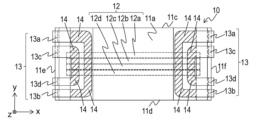
- 2A to 2C are external views of inductor 10 according to an embodiment of the present disclosure.
- FIG. 2A is a side view of inductor 10 viewed from the first side surface 11c side of inductor 10 according to an embodiment of the present disclosure.
- FIG. 2B is a bottom view of the inductor 10 viewed from the side of the bottom surface 11a of the inductor 10.
- FIG. FIG. 2C is an end view of the inductor 10 viewed from the first end face 11f side of the inductor 10.
- FIG. 2A to 2C the internal coil element 12 is indicated by broken lines.
- FIGS. 1 to 6 show an xyz orthogonal coordinate system.
- An inductor 10 includes a rectangular parallelepiped magnetic core 11 formed by mixing a magnetic material powder made of Fe—Si—Cr powder and a binder made of silicone and press-molding the magnetic core 11. and an embedded coil element 12 .
- the outer shape of the magnetic core 11 is a rectangular parallelepiped with a width (y-axis direction) of about 6 mm, a length (x-axis direction) of about 13 mm, and a height (z-axis direction) of about 5 mm.
- the magnetic core 11 includes a bottom surface 11a from which the ends of the coil elements 12 protrude, a top surface 11b facing the bottom surface 11a, a first side surface 11c connecting the bottom surface 11a and the top surface 11b, and a first side surface 11c. , a first end face 11e connecting the first side face 11c and the second side face 11d, and a second end face 11f facing the first end face 11e. .
- each coil element 12 each made of a flat plate are embedded inside the magnetic core 11 .
- a first coil element 12a, a second coil element 12b, a third coil element 12c, and a fourth coil element 12d are arranged in order from the first side surface 11c side of the magnetic core 11 toward the second side surface 11d side, Adjacent coil elements are embedded such that the side surfaces thereof are opposed to each other.
- An end portion of each coil element 12 protrudes from the bottom surface 11a of the magnetic core 11 and is bent along the bottom surface 11a to form an external electrode 13 .
- Each coil element 12 is formed by punching a copper plate, and has a thickness of about 0.4 mm and a coil pattern width of about 0.8 mm.
- an insulating layer 16 made of epoxy resin, phenol resin, acrylic resin, or the like and having a thickness of about 0.03 mm is provided by pad printing or the like.
- the external electrode connected to the first coil element 12a is the first external electrode 13a
- the external electrode connected to the second coil element 12b is the second external electrode 13b
- the external electrode connected to the third coil element 12c is the third external electrode.
- An external electrode connected to the third external electrode 13c and the fourth coil element 12d is called a fourth external electrode 13d.
- Each end of the first coil element 12a and each end of the third coil element 12c are bent toward the first side surface 11c to form the first external electrode 13a and the third external electrode 13c, respectively.
- Each end of the second coil element 12b and each end of the fourth coil element 12d are bent toward the second side surface 11d to form the second external electrode 13b and the fourth external electrode 13d, respectively.
- each of the first external electrode 13a, the second external electrode 13b, the third external electrode 13c, and the fourth external electrode 13d extends in the direction of the first end surface 11e or the second end surface 11f, that is, along the x-axis. direction, and the tip portion is bent along the first end surface 11e or the second end surface 11f.
- Inductor 10 with a small mounting area can be obtained by forming external electrode 13 by bending the ends of coil element 12 so as to protrude from bottom surface 11a.
- the bottom surface 11a of the magnetic core 11 is provided with a recess 15 having a depth of about 0.4 mm in a region that includes a portion where the coil element 12 protrudes and connects the first side surface 11c and the second side surface 11d. If the end of the coil element 12 protrudes from the bottom surface 11a and is bent along the bottom surface 11a, the bent portion inevitably bulges, resulting in poor mounting stability. Therefore, by protruding the ends of the coil elements 12 from the recesses 15 provided in the bottom surface 11a of the magnetic core 11 as in the present embodiment, the flatness of the mounting surface of the inductor can be improved.
- the depth of the concave portion 15 is desirably 80% or more and 200% or less of the thickness of the external electrode 13 . If the depth of the concave portion is shallower than 80% of the thickness of the external electrode, the flatness is deteriorated. Conversely, if it exceeds 200%, the volume of the core becomes small and the inductance value decreases, which is not preferable.
- the inductor 10 is configured as described above.
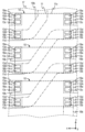
- FIG. 3 is a top perspective view when the inductor 10 of the present disclosure is mounted on the mounting board 17 and used.
- FIG. 3 shows an example of use in a three-phase multiphase voltage regulator.
- One inductor 10 is used for each phase.
- FIG. 3 shows the periphery of three inductors 10 of a three-phase multiphase voltage regulator.
- the three inductors 10 are arranged such that the first side 11c and the second side 11d face each other.
- a pad 18a and a pad 18b are provided on the mounting board 17 for each inductor.
- the mounting board 17 is indicated by a dashed line
- the pads 18a and 18b are indicated by broken lines
- the magnetic core 11 is indicated by long broken lines
- the first to fourth external electrodes 13a to 13d are indicated by solid lines.
- Adjacent first external electrode 13a and third external electrode 13c on mounting substrate 17 are connected by pad 18a to form first inductor 10A, and adjacent second external electrode 13b and fourth external electrode are connected.
- the electrode 13d is connected with the pad 18b to form the second inductor 10B.
- the second coil element 12b which is the second inductor 10B, is sandwiched between the first coil element 12a, which is the first inductor 10A, and the third coil element 12c.
- the third coil element 12c which is the first inductor 10A, is sandwiched between the second coil element 12b, which is the inductor 10B, and the fourth coil element 12d. Further, one coil element 12 (any one of the first coil element 12a to the fourth coil element 12d) is connected to at least one other coil element 12 ( At least one of the first coil element 12a to the fourth coil element 12d), so that the inductor 10 having a high coupling coefficient between the first inductor 10A and the second inductor 10B can be obtained. can be done.
- the wiring pattern 19a is indicated by a dotted line
- the wiring pattern 19b is indicated by a two-dot chain line.
- the wiring pattern 19a is connected to a regulator circuit for each phase of the multiphase voltage regulator.
- the wiring pattern 19b connects the three second inductors 10B in series.
- the wiring patterns 19b at both ends to which the three second inductors 10B are connected in series are each connected to the ground (GND).
- GND ground
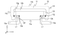
- FIG. 4A is a plan view of the first coil element 12a
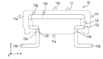
- FIG. 4B is a plan view of the second coil element 12b
- FIG. 4C is a plan view of the third coil element 12c
- FIG. 4D is a plan view of the fourth coil element 12d.
- FIGS. 4A to 4D broken lines show the outer shape of the magnetic core 11 when the first to fourth coil elements 12a to 12d are embedded in the magnetic core 11.
- FIG. The ends of the first to fourth coil elements 12a to 12d protruding outside the dashed line are embedded and then bent along the bottom surface 11a to form the first external electrodes 13a to the fourth coil elements 13a to 4th coil elements 12d, respectively. constitute the external electrode 13d.
- the boundaries between the first to seventh portions are indicated by dashed lines in order to make the regions of the first to seventh portions easier to understand.
- each of the first coil element 12a to the fourth coil element 12d has the configuration shown in (a) to (g) below.
- a third portion 12g connected to the end of the second portion 12f on the top surface 11b side and the first end surface 11e side and extending toward the top surface 11b side.
- a fifth portion 12i connected to the end of the fourth portion 12h on the bottom surface 11a side and the second end surface 11f side and extending toward the bottom surface 11a side.
- a sixth portion 12j connected to the end of the fifth portion 12i on the bottom surface 11a side and extending toward the first end surface 11e.
- a seventh portion 12k connected to the end of the sixth portion 12j on the bottom surface 11a side and the first end surface 11e side and extending toward the bottom surface 11a side.
- the ends of the first to fourth coil elements 12a to 12d on the side of the bottom surface 11a project from the ends of the first portion 12e and the seventh portion 12k to the bottom surface 11a of the magnetic core 11, By bending along the bottom surface 11a of the magnetic core 11, the first to fourth external electrodes 13a to 13d are formed, respectively.
- the lengths of the second portion 12f and the sixth portion 12j (L1 in FIG. 4A) of the first coil element 12a and the second coil element 12b are equal to those of the third coil element 12c and the fourth coil element 12d. is longer than the width of the coil pattern compared to the lengths of the second portion 12f and the sixth portion 12j (L2 in FIG. 4C).
- the first coil element 12a and the second coil element 12b overlap in all paths embedded in the magnetic core 11, and the third coil element 12c and the fourth coil element 12d are embedded in the magnetic core 11. are overlapped in all paths that are Furthermore, in the third portion 12g to the fifth portion 12i, the first coil element 12a, the second coil element 12b, the third coil element 12c, and the fourth coil element 12d all overlap. By doing so, a large coupling coefficient can be obtained between the first inductor 10A and the second inductor 10B.
- the third coil element 12c and the fourth coil element 12d do not form the first, second, sixth, and seventh parts, but extend the third part and the fifth part to the bottom surface. Although it may be formed, it is preferable that at least a part of the second and sixth portions of each coil element overlap each other because the coupling coefficient between the plurality of coils can be increased. Also, in FIGS. 4A to 4D, the loops of the coils are rectangular, but the loops may be rounded ⁇ -shaped.
- a region is formed on the bottom surface 11a in which the end of the second coil element 12b and the end of the third coil element 12c are closely opposed to each other. If the end portions of the second coil element 12b and the end portions of the third coil element 12c are conductive in these opposing regions, short circuits are likely to occur during mounting. Therefore, it is desirable to provide the insulating layer 14 in the region where the end of the second coil element 12b and the end of the third coil element 12c face each other. In FIG. 2B, the portion where the insulating layer 14 is provided is hatched for easy understanding. It is desirable that this insulating layer 14 be provided at the same time as the insulating layer is formed on the coil element 12 in the portion embedded in the magnetic core 11 . By doing so, the process can be simplified.
- FIG. 5 shows a bottom external view of inductor 10 viewed from the bottom surface 11a side of inductor 10 in a modification of the embodiment of the present disclosure.
- FIG. 6 is a perspective top view of the inductor 10 according to this modification when it is mounted on a mounting board 17 and used.
- the example of use shown in FIG. 6 shows an example of use in a three-phase multiphase voltage regulator, like the example of use described in FIG. One inductor 10 is used for each phase.
- FIG. 6 shows the periphery of three inductors 10 of a three-phase multiphase voltage regulator.
- the three inductors 10 are arranged such that the first side 11c and the second side 11d face each other.
- a pad 18a and a pad 18b are provided on the mounting board 17 for each inductor.
- the mounting substrate 17 is indicated by a dashed line
- the pads 18a and wiring pads 18b are indicated by broken lines
- the magnetic core 11 is indicated by long broken lines
- the first to fourth external electrodes 13a to 13d are indicated by solid lines.
- a wiring pattern 19a connected to the pad 18a of each inductor 10 and a wiring pattern 19b connected to the pad 18b are provided on the mounting substrate 17.
- the wiring pattern 19a is indicated by a dotted line
- the wiring pattern 19b is indicated by a two-dot chain line.
- the external electrodes 13 are drawn out to the first end surface 11e side or the second end surface 11f side, but as shown in FIG. Alternatively, it may be pulled out toward the second side surface 11d.
- the second external electrode 13b and the fourth external electrode 13d are led out to the second side surface 11d.
- the inductance values of the first inductor 10A and the second inductor 10B (the sum of the first coil element and the third coil element, and the second coil element and the fourth coil element) is about 120 nH
- the DC resistance of each of the first inductor 10A and the second inductor 10B is about 0.5 m ⁇
- the coupling coefficient is about 0.98. be able to.
- the inductor according to the present disclosure is industrially useful because it is small, can handle large currents, and has a large coupling coefficient.
Landscapes
- Engineering & Computer Science (AREA)
- Power Engineering (AREA)
- Microelectronics & Electronic Packaging (AREA)
- Coils Or Transformers For Communication (AREA)
Priority Applications (3)
| Application Number | Priority Date | Filing Date | Title |
|---|---|---|---|
| JP2023563530A JPWO2023095430A1 (https=) | 2021-11-29 | 2022-09-21 | |
| US18/710,209 US20250029776A1 (en) | 2021-11-29 | 2022-09-21 | Inductor |
| CN202280076018.2A CN118251740A (zh) | 2021-11-29 | 2022-09-21 | 电感器 |
Applications Claiming Priority (2)
| Application Number | Priority Date | Filing Date | Title |
|---|---|---|---|
| JP2021-192756 | 2021-11-29 | ||
| JP2021192756 | 2021-11-29 |
Publications (1)
| Publication Number | Publication Date |
|---|---|
| WO2023095430A1 true WO2023095430A1 (ja) | 2023-06-01 |
Family
ID=86539199
Family Applications (1)
| Application Number | Title | Priority Date | Filing Date |
|---|---|---|---|
| PCT/JP2022/035256 Ceased WO2023095430A1 (ja) | 2021-11-29 | 2022-09-21 | インダクタ |
Country Status (4)
| Country | Link |
|---|---|
| US (1) | US20250029776A1 (https=) |
| JP (1) | JPWO2023095430A1 (https=) |
| CN (1) | CN118251740A (https=) |
| WO (1) | WO2023095430A1 (https=) |
Cited By (1)
| Publication number | Priority date | Publication date | Assignee | Title |
|---|---|---|---|---|
| WO2024176532A1 (ja) * | 2023-02-24 | 2024-08-29 | パナソニックIpマネジメント株式会社 | インダクタ |
Families Citing this family (1)
| Publication number | Priority date | Publication date | Assignee | Title |
|---|---|---|---|---|
| CN119885698B (zh) * | 2025-03-31 | 2026-02-17 | 苏州元脑智能科技有限公司 | 电感结构的确定方法、存储介质、电子设备及程序产品 |
Citations (4)
| Publication number | Priority date | Publication date | Assignee | Title |
|---|---|---|---|---|
| JPS6379307A (ja) * | 1986-09-22 | 1988-04-09 | Murata Mfg Co Ltd | 積層トランス |
| JPH10335146A (ja) * | 1997-06-03 | 1998-12-18 | Tdk Corp | インダクタンス素子 |
| JP2019153642A (ja) * | 2018-03-01 | 2019-09-12 | 株式会社村田製作所 | 表面実装インダクタ |
| JP2021100098A (ja) * | 2019-09-20 | 2021-07-01 | 太陽誘電株式会社 | インダクタ |
-
2022
- 2022-09-21 US US18/710,209 patent/US20250029776A1/en active Pending
- 2022-09-21 WO PCT/JP2022/035256 patent/WO2023095430A1/ja not_active Ceased
- 2022-09-21 JP JP2023563530A patent/JPWO2023095430A1/ja active Pending
- 2022-09-21 CN CN202280076018.2A patent/CN118251740A/zh active Pending
Patent Citations (4)
| Publication number | Priority date | Publication date | Assignee | Title |
|---|---|---|---|---|
| JPS6379307A (ja) * | 1986-09-22 | 1988-04-09 | Murata Mfg Co Ltd | 積層トランス |
| JPH10335146A (ja) * | 1997-06-03 | 1998-12-18 | Tdk Corp | インダクタンス素子 |
| JP2019153642A (ja) * | 2018-03-01 | 2019-09-12 | 株式会社村田製作所 | 表面実装インダクタ |
| JP2021100098A (ja) * | 2019-09-20 | 2021-07-01 | 太陽誘電株式会社 | インダクタ |
Cited By (1)
| Publication number | Priority date | Publication date | Assignee | Title |
|---|---|---|---|---|
| WO2024176532A1 (ja) * | 2023-02-24 | 2024-08-29 | パナソニックIpマネジメント株式会社 | インダクタ |
Also Published As
| Publication number | Publication date |
|---|---|
| US20250029776A1 (en) | 2025-01-23 |
| JPWO2023095430A1 (https=) | 2023-06-01 |
| CN118251740A (zh) | 2024-06-25 |
Similar Documents
| Publication | Publication Date | Title |
|---|---|---|
| EP4057308B1 (en) | Multi-winding inductor and power supply module | |
| TWI539473B (zh) | 可變耦合電感器 | |
| US20180190573A1 (en) | Leadframe inductor | |
| WO2003015110A1 (en) | Planar inductive component and a planar transformer | |
| WO2023095430A1 (ja) | インダクタ | |
| CN103825367A (zh) | 无线电力传输装置 | |
| CN107039153A (zh) | 线圈部件及具备该线圈部件的电路基板 | |
| CN110534315B (zh) | 线圈组件 | |
| US12562304B2 (en) | Integrally-formed inductor and power supply module | |
| JP2008109139A (ja) | いくつかのコイルブランチを有するコイル、及び当該コイルの一つを有するマイクロインダクタ | |
| WO2024176532A1 (ja) | インダクタ | |
| CN110323838A (zh) | 线圈单元、无线供电装置、无线受电装置及无线电力传输系统 | |
| JP2010062409A (ja) | インダクター部品 | |
| KR20170125658A (ko) | 인덕터 및 이의 제조 방법 | |
| JP2021072421A (ja) | インダクタ | |
| TWI627642B (zh) | 可變耦合電感器 | |
| WO2023163168A1 (ja) | インダクタ | |
| JP2005064321A (ja) | コイル部品およびそれを搭載した電子機器 | |
| US20260128209A1 (en) | Integrally-formed inductor | |
| JP2024120375A (ja) | インダクタ | |
| CN106257601B (zh) | 可变耦合电感器 | |
| CN101211689B (zh) | 内藏电感组件及其制造方法 | |
| JP2025090071A (ja) | インダクタンス部品 | |
| CN118645333A (zh) | 层叠电感器 | |
| WO2025022939A1 (ja) | インダクタ |
Legal Events
| Date | Code | Title | Description |
|---|---|---|---|
| 121 | Ep: the epo has been informed by wipo that ep was designated in this application |
Ref document number: 22898215 Country of ref document: EP Kind code of ref document: A1 |
|
| ENP | Entry into the national phase |
Ref document number: 2023563530 Country of ref document: JP Kind code of ref document: A |
|
| WWE | Wipo information: entry into national phase |
Ref document number: 18710209 Country of ref document: US Ref document number: 202280076018.2 Country of ref document: CN |
|
| NENP | Non-entry into the national phase |
Ref country code: DE |
|
| 122 | Ep: pct application non-entry in european phase |
Ref document number: 22898215 Country of ref document: EP Kind code of ref document: A1 |