WO2023095430A1 - Inductor - Google Patents
Inductor Download PDFInfo
- Publication number
- WO2023095430A1 WO2023095430A1 PCT/JP2022/035256 JP2022035256W WO2023095430A1 WO 2023095430 A1 WO2023095430 A1 WO 2023095430A1 JP 2022035256 W JP2022035256 W JP 2022035256W WO 2023095430 A1 WO2023095430 A1 WO 2023095430A1
- Authority
- WO
- WIPO (PCT)
- Prior art keywords
- coil element
- external electrode
- inductor
- coil
- magnetic core
- Prior art date
Links
- 238000005452 bending Methods 0.000 claims description 5
- 239000000843 powder Substances 0.000 claims description 4
- 239000011230 binding agent Substances 0.000 claims description 3
- 239000000696 magnetic material Substances 0.000 claims description 3
- 238000000465 moulding Methods 0.000 claims description 2
- 239000000203 mixture Substances 0.000 claims 1
- 238000010168 coupling process Methods 0.000 abstract description 17
- 230000008878 coupling Effects 0.000 abstract description 15
- 238000005859 coupling reaction Methods 0.000 abstract description 15
- 239000000758 substrate Substances 0.000 description 6
- 230000004048 modification Effects 0.000 description 4
- 238000012986 modification Methods 0.000 description 4
- 238000000034 method Methods 0.000 description 3
- 239000004925 Acrylic resin Substances 0.000 description 1
- 229920000178 Acrylic resin Polymers 0.000 description 1
- RYGMFSIKBFXOCR-UHFFFAOYSA-N Copper Chemical compound [Cu] RYGMFSIKBFXOCR-UHFFFAOYSA-N 0.000 description 1
- 229910008458 Si—Cr Inorganic materials 0.000 description 1
- 229910052802 copper Inorganic materials 0.000 description 1
- 239000010949 copper Substances 0.000 description 1
- 230000007423 decrease Effects 0.000 description 1
- 238000010586 diagram Methods 0.000 description 1
- 239000003822 epoxy resin Substances 0.000 description 1
- 238000007649 pad printing Methods 0.000 description 1
- 239000005011 phenolic resin Substances 0.000 description 1
- 229920000647 polyepoxide Polymers 0.000 description 1
- 229920001296 polysiloxane Polymers 0.000 description 1
- 238000004080 punching Methods 0.000 description 1
Images


Classifications
-
- H—ELECTRICITY
- H01—ELECTRIC ELEMENTS
- H01F—MAGNETS; INDUCTANCES; TRANSFORMERS; SELECTION OF MATERIALS FOR THEIR MAGNETIC PROPERTIES
- H01F17/00—Fixed inductances of the signal type
- H01F17/04—Fixed inductances of the signal type with magnetic core
-
- H—ELECTRICITY
- H01—ELECTRIC ELEMENTS
- H01F—MAGNETS; INDUCTANCES; TRANSFORMERS; SELECTION OF MATERIALS FOR THEIR MAGNETIC PROPERTIES
- H01F27/00—Details of transformers or inductances, in general
-
- H—ELECTRICITY
- H01—ELECTRIC ELEMENTS
- H01F—MAGNETS; INDUCTANCES; TRANSFORMERS; SELECTION OF MATERIALS FOR THEIR MAGNETIC PROPERTIES
- H01F27/00—Details of transformers or inductances, in general
- H01F27/28—Coils; Windings; Conductive connections
- H01F27/29—Terminals; Tapping arrangements for signal inductances
Definitions
- the present disclosure relates to inductors used in power supply circuits and the like.
- a multi-phase power supply system has been mainly used in order to cope with the increase in current. Therefore, a coupling system has been used as a power supply system corresponding to this system.
- the inductor used in this coupling system is driven by an inductor in which a plurality of coils are coupled with a coupling coefficient of about 0.6.
- Patent Document 1 is known as prior art document information.
- An object of the present disclosure is to provide an inductor that is small, can handle large currents, and has a large coupling coefficient.
- the inductor of the present disclosure includes a rectangular parallelepiped magnetic core obtained by mixing magnetic material powder and a binder and press-forming, and a coil element embedded in the magnetic core.
- the magnetic core has a bottom surface, a top surface facing the bottom surface, a first side surface connecting the bottom surface and the top surface, and a second side surface facing the first side surface.
- At least four coil elements are provided to overlap the first coil element, the second coil element, the third coil element, and the fourth coil element in order from the first side surface side toward the second side surface side.
- a first coil element, a second coil element, a third coil element, and a fourth coil element are stacked in order from the first side surface side to the second side surface side.
- the ends of the first to fourth coil elements protrude from the bottom surface and are bent along the bottom surface to form external electrodes.
- the external electrode connected to the first coil element is the first external electrode
- the external electrode connected to the second coil element is the second external electrode
- the external electrode connected to the third coil element is the third external electrode
- the fourth The external electrode connected to the coil element of is the fourth external electrode.
- a first external electrode and a third external electrode are provided by bending each end of the first coil element and each end of the third coil element toward the first side surface.
- Each end of the second coil element and each end of the fourth coil element are bent toward the second side surface to provide a second external electrode and a fourth external electrode, respectively.
- FIG. 1 is a perspective view of an inductor according to an embodiment of the present disclosure
- FIG. Side view of an inductor according to an embodiment of the present disclosure A bottom view of an inductor according to an embodiment of the present disclosure
- FIG. 4 is an end view of an inductor in accordance with an embodiment of the present disclosure
- FIG. 2 is a top perspective view when the inductor according to the embodiment of the present disclosure is mounted on a mounting substrate and used;
- FIG. 4 is a plan view of a first coil element of an inductor according to an embodiment of the present disclosure; A plan view of a second coil element of an inductor according to an embodiment of the present disclosure A plan view of a third coil element of an inductor according to an embodiment of the present disclosure A plan view of a fourth coil element of an inductor according to an embodiment of the present disclosure
- FIG. 11 is a bottom side external view of an inductor in a modification of an embodiment of the present disclosure;
- FIG. 5 is a top perspective view when the inductor in the modified example of the embodiment of the present disclosure is mounted on a mounting substrate and used;
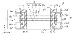
- FIG. 1 is a perspective view of the inductor 10 viewed from the bottom surface 11a side of the inductor 10 according to the embodiment of the present disclosure.
- 2A to 2C are external views of inductor 10 according to an embodiment of the present disclosure.
- FIG. 2A is a side view of inductor 10 viewed from the first side surface 11c side of inductor 10 according to an embodiment of the present disclosure.
- FIG. 2B is a bottom view of the inductor 10 viewed from the side of the bottom surface 11a of the inductor 10.
- FIG. FIG. 2C is an end view of the inductor 10 viewed from the first end face 11f side of the inductor 10.
- FIG. 2A to 2C the internal coil element 12 is indicated by broken lines.
- FIGS. 1 to 6 show an xyz orthogonal coordinate system.
- An inductor 10 includes a rectangular parallelepiped magnetic core 11 formed by mixing a magnetic material powder made of Fe—Si—Cr powder and a binder made of silicone and press-molding the magnetic core 11. and an embedded coil element 12 .
- the outer shape of the magnetic core 11 is a rectangular parallelepiped with a width (y-axis direction) of about 6 mm, a length (x-axis direction) of about 13 mm, and a height (z-axis direction) of about 5 mm.
- the magnetic core 11 includes a bottom surface 11a from which the ends of the coil elements 12 protrude, a top surface 11b facing the bottom surface 11a, a first side surface 11c connecting the bottom surface 11a and the top surface 11b, and a first side surface 11c. , a first end face 11e connecting the first side face 11c and the second side face 11d, and a second end face 11f facing the first end face 11e. .
- each coil element 12 each made of a flat plate are embedded inside the magnetic core 11 .
- a first coil element 12a, a second coil element 12b, a third coil element 12c, and a fourth coil element 12d are arranged in order from the first side surface 11c side of the magnetic core 11 toward the second side surface 11d side, Adjacent coil elements are embedded such that the side surfaces thereof are opposed to each other.
- An end portion of each coil element 12 protrudes from the bottom surface 11a of the magnetic core 11 and is bent along the bottom surface 11a to form an external electrode 13 .
- Each coil element 12 is formed by punching a copper plate, and has a thickness of about 0.4 mm and a coil pattern width of about 0.8 mm.
- an insulating layer 16 made of epoxy resin, phenol resin, acrylic resin, or the like and having a thickness of about 0.03 mm is provided by pad printing or the like.
- the external electrode connected to the first coil element 12a is the first external electrode 13a
- the external electrode connected to the second coil element 12b is the second external electrode 13b
- the external electrode connected to the third coil element 12c is the third external electrode.
- An external electrode connected to the third external electrode 13c and the fourth coil element 12d is called a fourth external electrode 13d.
- Each end of the first coil element 12a and each end of the third coil element 12c are bent toward the first side surface 11c to form the first external electrode 13a and the third external electrode 13c, respectively.
- Each end of the second coil element 12b and each end of the fourth coil element 12d are bent toward the second side surface 11d to form the second external electrode 13b and the fourth external electrode 13d, respectively.
- each of the first external electrode 13a, the second external electrode 13b, the third external electrode 13c, and the fourth external electrode 13d extends in the direction of the first end surface 11e or the second end surface 11f, that is, along the x-axis. direction, and the tip portion is bent along the first end surface 11e or the second end surface 11f.
- Inductor 10 with a small mounting area can be obtained by forming external electrode 13 by bending the ends of coil element 12 so as to protrude from bottom surface 11a.
- the bottom surface 11a of the magnetic core 11 is provided with a recess 15 having a depth of about 0.4 mm in a region that includes a portion where the coil element 12 protrudes and connects the first side surface 11c and the second side surface 11d. If the end of the coil element 12 protrudes from the bottom surface 11a and is bent along the bottom surface 11a, the bent portion inevitably bulges, resulting in poor mounting stability. Therefore, by protruding the ends of the coil elements 12 from the recesses 15 provided in the bottom surface 11a of the magnetic core 11 as in the present embodiment, the flatness of the mounting surface of the inductor can be improved.
- the depth of the concave portion 15 is desirably 80% or more and 200% or less of the thickness of the external electrode 13 . If the depth of the concave portion is shallower than 80% of the thickness of the external electrode, the flatness is deteriorated. Conversely, if it exceeds 200%, the volume of the core becomes small and the inductance value decreases, which is not preferable.
- the inductor 10 is configured as described above.
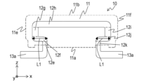
- FIG. 3 is a top perspective view when the inductor 10 of the present disclosure is mounted on the mounting board 17 and used.
- FIG. 3 shows an example of use in a three-phase multiphase voltage regulator.
- One inductor 10 is used for each phase.
- FIG. 3 shows the periphery of three inductors 10 of a three-phase multiphase voltage regulator.
- the three inductors 10 are arranged such that the first side 11c and the second side 11d face each other.
- a pad 18a and a pad 18b are provided on the mounting board 17 for each inductor.
- the mounting board 17 is indicated by a dashed line
- the pads 18a and 18b are indicated by broken lines
- the magnetic core 11 is indicated by long broken lines
- the first to fourth external electrodes 13a to 13d are indicated by solid lines.
- Adjacent first external electrode 13a and third external electrode 13c on mounting substrate 17 are connected by pad 18a to form first inductor 10A, and adjacent second external electrode 13b and fourth external electrode are connected.
- the electrode 13d is connected with the pad 18b to form the second inductor 10B.
- the second coil element 12b which is the second inductor 10B, is sandwiched between the first coil element 12a, which is the first inductor 10A, and the third coil element 12c.
- the third coil element 12c which is the first inductor 10A, is sandwiched between the second coil element 12b, which is the inductor 10B, and the fourth coil element 12d. Further, one coil element 12 (any one of the first coil element 12a to the fourth coil element 12d) is connected to at least one other coil element 12 ( At least one of the first coil element 12a to the fourth coil element 12d), so that the inductor 10 having a high coupling coefficient between the first inductor 10A and the second inductor 10B can be obtained. can be done.
- the wiring pattern 19a is indicated by a dotted line
- the wiring pattern 19b is indicated by a two-dot chain line.
- the wiring pattern 19a is connected to a regulator circuit for each phase of the multiphase voltage regulator.
- the wiring pattern 19b connects the three second inductors 10B in series.
- the wiring patterns 19b at both ends to which the three second inductors 10B are connected in series are each connected to the ground (GND).
- GND ground
- FIG. 4A is a plan view of the first coil element 12a
- FIG. 4B is a plan view of the second coil element 12b
- FIG. 4C is a plan view of the third coil element 12c
- FIG. 4D is a plan view of the fourth coil element 12d.
- FIGS. 4A to 4D broken lines show the outer shape of the magnetic core 11 when the first to fourth coil elements 12a to 12d are embedded in the magnetic core 11.
- FIG. The ends of the first to fourth coil elements 12a to 12d protruding outside the dashed line are embedded and then bent along the bottom surface 11a to form the first external electrodes 13a to the fourth coil elements 13a to 4th coil elements 12d, respectively. constitute the external electrode 13d.
- the boundaries between the first to seventh portions are indicated by dashed lines in order to make the regions of the first to seventh portions easier to understand.
- each of the first coil element 12a to the fourth coil element 12d has the configuration shown in (a) to (g) below.
- a third portion 12g connected to the end of the second portion 12f on the top surface 11b side and the first end surface 11e side and extending toward the top surface 11b side.
- a fifth portion 12i connected to the end of the fourth portion 12h on the bottom surface 11a side and the second end surface 11f side and extending toward the bottom surface 11a side.
- a sixth portion 12j connected to the end of the fifth portion 12i on the bottom surface 11a side and extending toward the first end surface 11e.
- a seventh portion 12k connected to the end of the sixth portion 12j on the bottom surface 11a side and the first end surface 11e side and extending toward the bottom surface 11a side.
- the ends of the first to fourth coil elements 12a to 12d on the side of the bottom surface 11a project from the ends of the first portion 12e and the seventh portion 12k to the bottom surface 11a of the magnetic core 11, By bending along the bottom surface 11a of the magnetic core 11, the first to fourth external electrodes 13a to 13d are formed, respectively.
- the lengths of the second portion 12f and the sixth portion 12j (L1 in FIG. 4A) of the first coil element 12a and the second coil element 12b are equal to those of the third coil element 12c and the fourth coil element 12d. is longer than the width of the coil pattern compared to the lengths of the second portion 12f and the sixth portion 12j (L2 in FIG. 4C).
- the first coil element 12a and the second coil element 12b overlap in all paths embedded in the magnetic core 11, and the third coil element 12c and the fourth coil element 12d are embedded in the magnetic core 11. are overlapped in all paths that are Furthermore, in the third portion 12g to the fifth portion 12i, the first coil element 12a, the second coil element 12b, the third coil element 12c, and the fourth coil element 12d all overlap. By doing so, a large coupling coefficient can be obtained between the first inductor 10A and the second inductor 10B.
- the third coil element 12c and the fourth coil element 12d do not form the first, second, sixth, and seventh parts, but extend the third part and the fifth part to the bottom surface. Although it may be formed, it is preferable that at least a part of the second and sixth portions of each coil element overlap each other because the coupling coefficient between the plurality of coils can be increased. Also, in FIGS. 4A to 4D, the loops of the coils are rectangular, but the loops may be rounded ⁇ -shaped.
- a region is formed on the bottom surface 11a in which the end of the second coil element 12b and the end of the third coil element 12c are closely opposed to each other. If the end portions of the second coil element 12b and the end portions of the third coil element 12c are conductive in these opposing regions, short circuits are likely to occur during mounting. Therefore, it is desirable to provide the insulating layer 14 in the region where the end of the second coil element 12b and the end of the third coil element 12c face each other. In FIG. 2B, the portion where the insulating layer 14 is provided is hatched for easy understanding. It is desirable that this insulating layer 14 be provided at the same time as the insulating layer is formed on the coil element 12 in the portion embedded in the magnetic core 11 . By doing so, the process can be simplified.
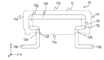
- FIG. 5 shows a bottom external view of inductor 10 viewed from the bottom surface 11a side of inductor 10 in a modification of the embodiment of the present disclosure.
- FIG. 6 is a perspective top view of the inductor 10 according to this modification when it is mounted on a mounting board 17 and used.
- the example of use shown in FIG. 6 shows an example of use in a three-phase multiphase voltage regulator, like the example of use described in FIG. One inductor 10 is used for each phase.
- FIG. 6 shows the periphery of three inductors 10 of a three-phase multiphase voltage regulator.
- the three inductors 10 are arranged such that the first side 11c and the second side 11d face each other.
- a pad 18a and a pad 18b are provided on the mounting board 17 for each inductor.
- the mounting substrate 17 is indicated by a dashed line
- the pads 18a and wiring pads 18b are indicated by broken lines
- the magnetic core 11 is indicated by long broken lines
- the first to fourth external electrodes 13a to 13d are indicated by solid lines.
- a wiring pattern 19a connected to the pad 18a of each inductor 10 and a wiring pattern 19b connected to the pad 18b are provided on the mounting substrate 17.
- the wiring pattern 19a is indicated by a dotted line
- the wiring pattern 19b is indicated by a two-dot chain line.
- the external electrodes 13 are drawn out to the first end surface 11e side or the second end surface 11f side, but as shown in FIG. Alternatively, it may be pulled out toward the second side surface 11d.
- the second external electrode 13b and the fourth external electrode 13d are led out to the second side surface 11d.
- the inductance values of the first inductor 10A and the second inductor 10B (the sum of the first coil element and the third coil element, and the second coil element and the fourth coil element) is about 120 nH
- the DC resistance of each of the first inductor 10A and the second inductor 10B is about 0.5 m ⁇
- the coupling coefficient is about 0.98. be able to.
- the inductor according to the present disclosure is industrially useful because it is small, can handle large currents, and has a large coupling coefficient.
Abstract
The purpose of the present invention is to obtain an inductor which has a small size, can deal with a large current, and has a large coupling coefficient. This inductor (10) comprises a magnetic core (11) and a coil element (12) embedded in the magnetic core (11). The coil element (12) is composed of at least four flat plate coils in which a first coil element (12a), a second coil element (12b), a third coil element (12c), and a fourth coil element (12d) are provided in a superimposed manner. End sections of the coil element (12) each protrude from a bottom surface (11a) and are bent along the bottom surface (11a), thereby forming an external electrode (13). End sections of the first coil element (12a) and end sections of the third coil element (12c) are bent toward a first side surface (11c). End sections of the second coil element (12b) and end sections of the fourth coil element (12d) are bent toward a second side surface (11d).
Description
本開示は、電源回路等に用いられるインダクタに関するものである。
The present disclosure relates to inductors used in power supply circuits and the like.
近年CPU(Central Processing Unit)などの大規模集積回路は、低電圧化が進み、素子に必要とされる所要電流が数十アンペアにまで達するようになるとともに、小型で低背の電源回路が求められている。大電流化に対応するためマルチフェーズの電源方式が主流として使われてきた。そのためこの方式に対応する電源方式としてカップリング方式が用いられてきた。このカップリング方式に使われるインダクタは、複数のコイルが結合係数0.6程度で結合されたインダクタで駆動される。
In recent years, large-scale integrated circuits such as CPUs (Central Processing Units) have become increasingly low voltage, and the required current for the elements has reached several tens of amperes. It is A multi-phase power supply system has been mainly used in order to cope with the increase in current. Therefore, a coupling system has been used as a power supply system corresponding to this system. The inductor used in this coupling system is driven by an inductor in which a plurality of coils are coupled with a coupling coefficient of about 0.6.
なお、先行技術文献情報として、例えば、特許文献1が知られている。
For example, Patent Document 1 is known as prior art document information.
しかしながらさらに大電流化が要望されると従来のカップリング方式では限界があった。これに対して多相電圧レギュレータと呼ばれる方式が検討されている。この方式の場合複数のコイル間の結合を大幅に大きくする必要があり、カップリング方式に用いられているインダクタでは十分な特性を得ることができなかった。結合係数を上げるためには複数のコイル間の対向面積を大きくする必要があり、従来のカップルドインダクタのような電極取り出しを行うことが難しかった。
However, there were limits to the conventional coupling method when there was a demand for even higher currents. On the other hand, a method called a polyphase voltage regulator is being studied. In this method, it is necessary to significantly increase the coupling between the coils, and the inductor used in the coupling method cannot obtain sufficient characteristics. In order to increase the coupling coefficient, it was necessary to increase the facing area between the multiple coils, and it was difficult to extract the electrodes as in the conventional coupled inductor.
本開示は、小型で大電流に対応でき、結合係数の大きなインダクタを提供することを目的としている。
An object of the present disclosure is to provide an inductor that is small, can handle large currents, and has a large coupling coefficient.
上記問題を解決するために、本開示のインダクタは、磁性材料粉と結合剤とを混合して加圧成形した直方体状の磁心と、磁心に埋設されたコイル素子と、を備える。磁心は底面と、底面に対向する天面と、底面と天面とをつなぐ第1の側面と、第1の側面に対向する第2の側面とを有する。コイル素子は、第1の側面側から第2の側面側に向けて順に第1のコイル素子、第2のコイル素子、第3のコイル素子、第4のコイル素子と重ねて設けた、少なくとも4個の平板コイルからなり、第1の側面側から第2の側面側に向けて順に第1のコイル素子、第2のコイル素子、第3のコイル素子、第4のコイル素子と重ねて設けている。第1~第4のコイル素子の端部はそれぞれ底面から突出して底面に沿って折り曲げられて外部電極を構成する。第1のコイル素子につながる外部電極を第1の外部電極、第2のコイル素子につながる外部電極を第2の外部電極、第3のコイル素子につながる外部電極を第3の外部電極、第4のコイル素子につながる外部電極を第4の外部電極とする。第1のコイル素子の各端部および第3のコイル素子の各端部が第1の側面に向けて折り曲げられることにより、それぞれ第1の外部電極および第3の外部電極が設けられる。第2のコイル素子の各端部および第4のコイル素子の各端部が第2の側面に向けて折り曲げられることにより、それぞれ第2の外部電極および第4の外部電極が設けられる。
In order to solve the above problem, the inductor of the present disclosure includes a rectangular parallelepiped magnetic core obtained by mixing magnetic material powder and a binder and press-forming, and a coil element embedded in the magnetic core. The magnetic core has a bottom surface, a top surface facing the bottom surface, a first side surface connecting the bottom surface and the top surface, and a second side surface facing the first side surface. At least four coil elements are provided to overlap the first coil element, the second coil element, the third coil element, and the fourth coil element in order from the first side surface side toward the second side surface side. A first coil element, a second coil element, a third coil element, and a fourth coil element are stacked in order from the first side surface side to the second side surface side. there is The ends of the first to fourth coil elements protrude from the bottom surface and are bent along the bottom surface to form external electrodes. The external electrode connected to the first coil element is the first external electrode, the external electrode connected to the second coil element is the second external electrode, the external electrode connected to the third coil element is the third external electrode, and the fourth The external electrode connected to the coil element of is the fourth external electrode. A first external electrode and a third external electrode are provided by bending each end of the first coil element and each end of the third coil element toward the first side surface. Each end of the second coil element and each end of the fourth coil element are bent toward the second side surface to provide a second external electrode and a fourth external electrode, respectively.
上記構成により小型で大電流に対応でき、結合係数の大きなインダクタを提供することができる。
With the above configuration, it is possible to provide an inductor that is compact, can handle large currents, and has a large coupling coefficient.
以下、本開示の一実施の形態におけるインダクタ10について、図面を参照しながら説明する。
An inductor 10 according to an embodiment of the present disclosure will be described below with reference to the drawings.
図1は本開示の一実施の形態におけるインダクタ10の底面11a側からインダクタ10を見たときの斜視図である。図2A~図2Cは本開示の一実施の形態におけるインダクタ10の外観図である。図2Aは本開示の一実施の形態におけるインダクタ10の第1の側面11c側からインダクタ10を見たときの側面図である。図2Bはインダクタ10の底面11a側からインダクタ10を見たときの下面図である。図2Cはインダクタ10の第1の端面11f側からインダクタ10を見たときの端面図である。なお図2A~図2Cでは内部のコイル素子12は破線で示している。なお、図1~図6におけるインダクタ10に関し、第1の端面11eから第2の端面11fへ向かう方向を正の方向としてx軸を設け、第4のコイル素子12dから第1のコイル素子12aへ向かう方向を正の方向としてy軸を設け、インダクタ10の底面11aから天面11bへ向かう方向を正の方向としてz軸を設けることとする。すなわち、図1~図6にはxyz直交座標系が示されている。
FIG. 1 is a perspective view of the inductor 10 viewed from the bottom surface 11a side of the inductor 10 according to the embodiment of the present disclosure. 2A to 2C are external views of inductor 10 according to an embodiment of the present disclosure. FIG. 2A is a side view of inductor 10 viewed from the first side surface 11c side of inductor 10 according to an embodiment of the present disclosure. FIG. 2B is a bottom view of the inductor 10 viewed from the side of the bottom surface 11a of the inductor 10. FIG. FIG. 2C is an end view of the inductor 10 viewed from the first end face 11f side of the inductor 10. FIG. 2A to 2C, the internal coil element 12 is indicated by broken lines. Regarding the inductor 10 in FIGS. 1 to 6, the direction from the first end surface 11e to the second end surface 11f is set as the positive direction, and the x-axis is provided. The y-axis is provided with the facing direction as the positive direction, and the z-axis is provided with the direction from the bottom surface 11a to the top surface 11b of the inductor 10 as the positive direction. That is, FIGS. 1 to 6 show an xyz orthogonal coordinate system.
本開示の一実施の形態におけるインダクタ10は、Fe-Si-Crの粉からなる磁性材料粉とシリコーンからなる結合剤とを混合して加圧成形した直方体状の磁心11と、この磁心11に埋設されたコイル素子12とからなっている。磁心11の外形形状は幅(y軸方向)約6mm、長さ(x軸方向)約13mm、高さ(z軸方向)約5mmの直方体状である。また、磁心11は、コイル素子12の端部が突出する底面11aと、底面11aに対向する天面11bと、底面11aと天面11bとをつなぐ第1の側面11cと、第1の側面11cに対向する第2の側面11dと、第1の側面11cと第2の側面11dとをつなぐ第1の端面11eと、第1の端面11eに対向する第2の端面11fとを有している。
An inductor 10 according to an embodiment of the present disclosure includes a rectangular parallelepiped magnetic core 11 formed by mixing a magnetic material powder made of Fe—Si—Cr powder and a binder made of silicone and press-molding the magnetic core 11. and an embedded coil element 12 . The outer shape of the magnetic core 11 is a rectangular parallelepiped with a width (y-axis direction) of about 6 mm, a length (x-axis direction) of about 13 mm, and a height (z-axis direction) of about 5 mm. Further, the magnetic core 11 includes a bottom surface 11a from which the ends of the coil elements 12 protrude, a top surface 11b facing the bottom surface 11a, a first side surface 11c connecting the bottom surface 11a and the top surface 11b, and a first side surface 11c. , a first end face 11e connecting the first side face 11c and the second side face 11d, and a second end face 11f facing the first end face 11e. .
磁心11の内部には、それぞれ平板よりなる4個のコイル素子12が埋設されている。磁心11の第1の側面11c側から第2の側面11d側に向けて順に、第1のコイル素子12a、第2のコイル素子12b、第3のコイル素子12c、第4のコイル素子12dが、それぞれ隣接コイル素子の側面が対向するように埋設されている。各コイル素子12の端部はそれぞれ磁心11の底面11aから突出し、底面11aに沿って折り曲げられることによって外部電極13を構成している。各コイル素子12は、銅板を打ち抜いて形成されたもので、厚さ約0.4mm、コイルパターンの幅を約0.8mmとしている。さらに磁心11に埋設される部分の各コイル素子12の表面は、厚さ約0.03mmのエポキシ樹脂、フェノール樹脂またはアクリル樹脂等からなる絶縁層16がパッド印刷等により設けられている。
Four coil elements 12 each made of a flat plate are embedded inside the magnetic core 11 . A first coil element 12a, a second coil element 12b, a third coil element 12c, and a fourth coil element 12d are arranged in order from the first side surface 11c side of the magnetic core 11 toward the second side surface 11d side, Adjacent coil elements are embedded such that the side surfaces thereof are opposed to each other. An end portion of each coil element 12 protrudes from the bottom surface 11a of the magnetic core 11 and is bent along the bottom surface 11a to form an external electrode 13 . Each coil element 12 is formed by punching a copper plate, and has a thickness of about 0.4 mm and a coil pattern width of about 0.8 mm. Furthermore, on the surface of each coil element 12 embedded in the magnetic core 11, an insulating layer 16 made of epoxy resin, phenol resin, acrylic resin, or the like and having a thickness of about 0.03 mm is provided by pad printing or the like.
ここで第1のコイル素子12aにつながる外部電極を第1の外部電極13a、第2のコイル素子12bにつながる外部電極を第2の外部電極13b、第3のコイル素子12cにつながる外部電極を第3の外部電極13c、第4のコイル素子12dにつながる外部電極を第4の外部電極13dと称する。第1のコイル素子12aの各端部および第3のコイル素子12cの各端部は第1の側面11cに向けて折り曲げられることにより、それぞれ第1の外部電極13aおよび第3の外部電極13cを構成する。第2のコイル素子12bの各端部および第4のコイル素子12dの各端部は第2の側面11dに向けて折り曲げられることにより、それぞれ第2の外部電極13bおよび第4の外部電極13dを構成する。さらに第1の外部電極13a、第2の外部電極13b、第3の外部電極13c、第4の外部電極13dの各々は、第1の端面11eまたは第2の端面11fの方向すなわちx軸に沿う方向に延伸され、先端部分が第1の端面11eまたは第2の端面11fに沿って折り曲げられている。このようにコイル素子12の端部を底面11aから突出させて折り曲げて外部電極13を構成することにより、実装面積の小さいインダクタ10を得ることができる。
Here, the external electrode connected to the first coil element 12a is the first external electrode 13a, the external electrode connected to the second coil element 12b is the second external electrode 13b, and the external electrode connected to the third coil element 12c is the third external electrode. An external electrode connected to the third external electrode 13c and the fourth coil element 12d is called a fourth external electrode 13d. Each end of the first coil element 12a and each end of the third coil element 12c are bent toward the first side surface 11c to form the first external electrode 13a and the third external electrode 13c, respectively. Configure. Each end of the second coil element 12b and each end of the fourth coil element 12d are bent toward the second side surface 11d to form the second external electrode 13b and the fourth external electrode 13d, respectively. Configure. Furthermore, each of the first external electrode 13a, the second external electrode 13b, the third external electrode 13c, and the fourth external electrode 13d extends in the direction of the first end surface 11e or the second end surface 11f, that is, along the x-axis. direction, and the tip portion is bent along the first end surface 11e or the second end surface 11f. Inductor 10 with a small mounting area can be obtained by forming external electrode 13 by bending the ends of coil element 12 so as to protrude from bottom surface 11a.
また磁心11の底面11aには、コイル素子12が突出する部分を含み、第1の側面11cと第2の側面11dとをつなぐ領域に深さ約0.4mmの凹部15を設けている。底面11aからコイル素子12の端部を突出させ、底面11aに沿って曲げると、どうしても曲げる部分でふくらみが生じ、実装するときに安定性が悪くなる。そこで本実施の形態のように、磁心11の底面11aに設けた凹部15からコイル素子12の端部を突出させることにより、このインダクタの実装面の平坦性を向上させることができる。凹部15の深さは、外部電極13の厚みの80%以上、200%以下とすることが望ましい。凹部の深さが外部電極の厚みの80%よりも浅くなると平坦性が悪くなる。逆に200%を超えるとコアの体積が小さくなってインダクタンス値が下がってしまうので好ましくない。
In addition, the bottom surface 11a of the magnetic core 11 is provided with a recess 15 having a depth of about 0.4 mm in a region that includes a portion where the coil element 12 protrudes and connects the first side surface 11c and the second side surface 11d. If the end of the coil element 12 protrudes from the bottom surface 11a and is bent along the bottom surface 11a, the bent portion inevitably bulges, resulting in poor mounting stability. Therefore, by protruding the ends of the coil elements 12 from the recesses 15 provided in the bottom surface 11a of the magnetic core 11 as in the present embodiment, the flatness of the mounting surface of the inductor can be improved. The depth of the concave portion 15 is desirably 80% or more and 200% or less of the thickness of the external electrode 13 . If the depth of the concave portion is shallower than 80% of the thickness of the external electrode, the flatness is deteriorated. Conversely, if it exceeds 200%, the volume of the core becomes small and the inductance value decreases, which is not preferable.
以上のようにインダクタ10を構成する。
The inductor 10 is configured as described above.
図3は、本開示のインダクタ10を実装基板17に実装して使用したときの上面透視図である。図3では、3相の多相電圧レギュレータに使用した場合の例を示している。インダクタ10は1相毎に1個用いられる。図3では、3相の多相電圧レギュレータの3つのインダクタ10の周辺を示している。3つのインダクタ10は、第1の側面11cと第2の側面11dが対向するように配置されている。1個のインダクタ毎にパッド18aおよびパッド18bが、実装基板17上に設けられている。図3において、実装基板17は一点鎖線、パッド18aおよびパッド18bは破線、磁心11は長破線、第1の外部電極13a~第4の外部電極13dは実線にて示されている。実装基板17上で隣り合う第1の外部電極13aと第3の外部電極13cとをパッド18aでつなぎ合わせて第1のインダクタ10Aを形成し、隣り合う第2の外部電極13bと第4の外部電極13dとをパッド18bでつなぎ合わせて第2のインダクタ10Bを形成するようにして使用する。このようにすることにより、第1のインダクタ10Aである第1のコイル素子12aと第3のコイル素子12cとの間に第2のインダクタ10Bである第2のコイル素子12bが挟まれ、第2のインダクタ10Bである第2のコイル素子12bと第4のコイル素子12dとの間に第1のインダクタ10Aである第3のコイル素子12cが挟まれている状態となっている。さらに磁心11の中に埋設されているすべての領域にわたって一つのコイル素子12(第1のコイル素子12a~第4のコイル素子12dのうちいずれか1つ)が少なくとも一つの他のコイル素子12(第1のコイル素子12a~第4のコイル素子12dのうち少なくとも1つ)と重なり合う状態となるため、第1のインダクタ10Aと第2のインダクタ10Bとの間で結合係数が高いインダクタ10を得ることができる。
FIG. 3 is a top perspective view when the inductor 10 of the present disclosure is mounted on the mounting board 17 and used. FIG. 3 shows an example of use in a three-phase multiphase voltage regulator. One inductor 10 is used for each phase. FIG. 3 shows the periphery of three inductors 10 of a three-phase multiphase voltage regulator. The three inductors 10 are arranged such that the first side 11c and the second side 11d face each other. A pad 18a and a pad 18b are provided on the mounting board 17 for each inductor. In FIG. 3, the mounting board 17 is indicated by a dashed line, the pads 18a and 18b are indicated by broken lines, the magnetic core 11 is indicated by long broken lines, and the first to fourth external electrodes 13a to 13d are indicated by solid lines. Adjacent first external electrode 13a and third external electrode 13c on mounting substrate 17 are connected by pad 18a to form first inductor 10A, and adjacent second external electrode 13b and fourth external electrode are connected. The electrode 13d is connected with the pad 18b to form the second inductor 10B. By doing so, the second coil element 12b, which is the second inductor 10B, is sandwiched between the first coil element 12a, which is the first inductor 10A, and the third coil element 12c. The third coil element 12c, which is the first inductor 10A, is sandwiched between the second coil element 12b, which is the inductor 10B, and the fourth coil element 12d. Further, one coil element 12 (any one of the first coil element 12a to the fourth coil element 12d) is connected to at least one other coil element 12 ( At least one of the first coil element 12a to the fourth coil element 12d), so that the inductor 10 having a high coupling coefficient between the first inductor 10A and the second inductor 10B can be obtained. can be done.
そして、図3に示した3相の多層電圧レギュレータの例では、各インダクタ10のパッド18aにつながる配線パターン19aおよびパッド18bにつながる配線パターン19bが実装基板17上に設けられている。図3において、配線パターン19aは点線、配線パターン19bは二点鎖線にて示されている。配線パターン19aは、それぞれ多相電圧レギュレータの1相毎のレギュレータ回路に接続される。また、配線パターン19bは、3つの第2のインダクタ10Bを直列に接続している。この、3つの第2のインダクタ10Bが直列に接続された両端の配線パターン19bは、それぞれグランド(GND)に接続される。3つの第2のインダクタ10Bが直列に接続されことによって3つの第1のインダクタ10Aを磁気結合させて使用する。本実施の形態では、第1のインダクタ10Aと第2のインダクタ10Bとの間で結合係数を高くできるため、3つの第1のインダクタ10A相互の磁気結合を高くすることができる。
In the example of the three-phase multi-layer voltage regulator shown in FIG. In FIG. 3, the wiring pattern 19a is indicated by a dotted line, and the wiring pattern 19b is indicated by a two-dot chain line. The wiring pattern 19a is connected to a regulator circuit for each phase of the multiphase voltage regulator. Also, the wiring pattern 19b connects the three second inductors 10B in series. The wiring patterns 19b at both ends to which the three second inductors 10B are connected in series are each connected to the ground (GND). By connecting the three second inductors 10B in series, the three first inductors 10A are magnetically coupled for use. In this embodiment, since the coupling coefficient between the first inductor 10A and the second inductor 10B can be increased, the mutual magnetic coupling between the three first inductors 10A can be increased.
ここでコイル素子12についてさらに詳細に説明する。図4Aは第1のコイル素子12aの平面図、図4Bは第2のコイル素子12bの平面図、図4Cは第3のコイル素子12cの平面図、図4Dは第4のコイル素子12dの平面図である。図4A~図4Dでは、これらの第1のコイル素子12a~第4のコイル素子12dが磁心11に埋設された時の磁心11の外形を破線で示している。破線の外に突出している第1のコイル素子12a~第4のコイル素子12dの端部は、埋設された後、底面11aに沿って折り曲げられることにより、それぞれ第1の外部電極13a~第4の外部電極13dを構成する。また図4A~図4Dでは第1の部分~第7の部分の領域をわかりやすくするため、それらの境界を一点鎖線で示している。
Here, the coil element 12 will be explained in more detail. 4A is a plan view of the first coil element 12a, FIG. 4B is a plan view of the second coil element 12b, FIG. 4C is a plan view of the third coil element 12c, and FIG. 4D is a plan view of the fourth coil element 12d. It is a diagram. In FIGS. 4A to 4D, broken lines show the outer shape of the magnetic core 11 when the first to fourth coil elements 12a to 12d are embedded in the magnetic core 11. FIG. The ends of the first to fourth coil elements 12a to 12d protruding outside the dashed line are embedded and then bent along the bottom surface 11a to form the first external electrodes 13a to the fourth coil elements 13a to 4th coil elements 12d, respectively. constitute the external electrode 13d. In addition, in FIGS. 4A to 4D, the boundaries between the first to seventh portions are indicated by dashed lines in order to make the regions of the first to seventh portions easier to understand.
第1のコイル素子12a~第4のコイル素子12dの各々は、磁心11の内部において、それぞれ、以下の(a)~(g)に示す構成を有する。
Inside the magnetic core 11, each of the first coil element 12a to the fourth coil element 12d has the configuration shown in (a) to (g) below.
(a)底面11aから天面11bに向かって延びる第1の部分12e。
(a) A first portion 12e extending from the bottom surface 11a toward the top surface 11b.
(b)第1の部分12eの天面11b側の端につながり第1の端面11e側に延びる第2の部分12f。
(b) A second portion 12f connected to the end of the first portion 12e on the side of the top surface 11b and extending toward the first end surface 11e.
(c)第2の部分12fの天面11b側かつ第1の端面11e側の端につながり天面11b側に延びる第3の部分12g。
(c) A third portion 12g connected to the end of the second portion 12f on the top surface 11b side and the first end surface 11e side and extending toward the top surface 11b side.
(d)第3の部分12gの天面11b側の端につながり第2の端面11f側に延びる第4の部分12h。
(d) A fourth portion 12h connected to the top surface 11b side end of the third portion 12g and extending toward the second end surface 11f side.
(e)第4の部分12hの底面11a側かつ第2の端面11f側の端につながり底面11a側に延びる第5の部分12i。
(e) A fifth portion 12i connected to the end of the fourth portion 12h on the bottom surface 11a side and the second end surface 11f side and extending toward the bottom surface 11a side.
(f)第5の部分12iの底面11a側の端につながり第1の端面11e側に延びる第6の部分12j。
(f) A sixth portion 12j connected to the end of the fifth portion 12i on the bottom surface 11a side and extending toward the first end surface 11e.
(g)第6の部分12jの底面11a側かつ第1の端面11e側の端につながり底面11a側に延びる第7の部分12k。
(g) A seventh portion 12k connected to the end of the sixth portion 12j on the bottom surface 11a side and the first end surface 11e side and extending toward the bottom surface 11a side.
また、第1のコイル素子12a~第4のコイル素子12dのそれぞれの底面11a側の端部は、それぞれ第1の部分12eおよび第7の部分12kの端から磁心11の底面11aに突出され、磁心11の底面11aに沿って折り曲げられることにより、それぞれ第1の外部電極13a~第4の外部電極13dを構成している。
The ends of the first to fourth coil elements 12a to 12d on the side of the bottom surface 11a project from the ends of the first portion 12e and the seventh portion 12k to the bottom surface 11a of the magnetic core 11, By bending along the bottom surface 11a of the magnetic core 11, the first to fourth external electrodes 13a to 13d are formed, respectively.
第1のコイル素子12aおよび第2のコイル素子12bの、第2の部分12fおよび第6の部分12jの長さ(図4AのL1)は、第3のコイル素子12cおよび第4のコイル素子12dの、第2の部分12fおよび第6の部分12jの長さ(図4CのL2)に比べて、コイルパターンの幅の分よりも長く形成されている。
The lengths of the second portion 12f and the sixth portion 12j (L1 in FIG. 4A) of the first coil element 12a and the second coil element 12b are equal to those of the third coil element 12c and the fourth coil element 12d. is longer than the width of the coil pattern compared to the lengths of the second portion 12f and the sixth portion 12j (L2 in FIG. 4C).
そして第1のコイル素子12aと第2のコイル素子12bとは、磁心11に埋設されているすべての経路で重なり合い、第3のコイル素子12cと第4のコイル素子12dとは、磁心11に埋設されているすべての経路で重なり合っている。さらに第3の部分12g~第5の部分12iでは、第1のコイル素子12a、第2のコイル素子12b、第3のコイル素子12c、および第4のコイル素子12dがすべて重なり合っている。このようにすることにより、第1のインダクタ10Aと第2のインダクタ10Bとの間で大きな結合係数を得ることができる。
The first coil element 12a and the second coil element 12b overlap in all paths embedded in the magnetic core 11, and the third coil element 12c and the fourth coil element 12d are embedded in the magnetic core 11. are overlapped in all paths that are Furthermore, in the third portion 12g to the fifth portion 12i, the first coil element 12a, the second coil element 12b, the third coil element 12c, and the fourth coil element 12d all overlap. By doing so, a large coupling coefficient can be obtained between the first inductor 10A and the second inductor 10B.
なお、第3のコイル素子12cと第4のコイル素子12dは、第1、第2、第6、第7の部分を形成せずに、第3の部分、第5の部分を底面まで延ばして形成してもよいが、各コイル素子の第2および第6の部分の少なくとも一部が重なることにより、複数のコイル間の結合係数を大きくできるので好ましい。また図4A~図4Dでは、コイルのループが矩形状となっているが、ループに丸みを帯びたΩ字状としても構わない。
The third coil element 12c and the fourth coil element 12d do not form the first, second, sixth, and seventh parts, but extend the third part and the fifth part to the bottom surface. Although it may be formed, it is preferable that at least a part of the second and sixth portions of each coil element overlap each other because the coupling coefficient between the plurality of coils can be increased. Also, in FIGS. 4A to 4D, the loops of the coils are rectangular, but the loops may be rounded Ω-shaped.
以上に説明した構成により、底面11aで第2のコイル素子12bの端部と第3のコイル素子12cの端部とが近接して対向する領域ができる。この対向する領域で第2のコイル素子12bの端部および第3のコイル素子12cの端部が導電性を有する状態となっていると、実装時に短絡が起こりやすくなる。そこで第2のコイル素子12bの端部と第3のコイル素子12cの端部とが対向する領域に絶縁層14を設けておくことが望ましい。なお図2Bでは、わかりやすくするために絶縁層14を設けた部分に斜線を施している。この絶縁層14は磁心11に埋設される部分のコイル素子12に絶縁層を形成するときに同時に設けておくことが望ましい。このようにすることにより工程の簡略化を図ることができる。
With the configuration described above, a region is formed on the bottom surface 11a in which the end of the second coil element 12b and the end of the third coil element 12c are closely opposed to each other. If the end portions of the second coil element 12b and the end portions of the third coil element 12c are conductive in these opposing regions, short circuits are likely to occur during mounting. Therefore, it is desirable to provide the insulating layer 14 in the region where the end of the second coil element 12b and the end of the third coil element 12c face each other. In FIG. 2B, the portion where the insulating layer 14 is provided is hatched for easy understanding. It is desirable that this insulating layer 14 be provided at the same time as the insulating layer is formed on the coil element 12 in the portion embedded in the magnetic core 11 . By doing so, the process can be simplified.
(変形例)
図5に本開示の一実施の形態の変形例におけるインダクタ10の底面11a側からインダクタ10を見たときの底面側外観図を示す。図6は、この変形例にかかるインダクタ10を実装基板17に実装して使用したときの上面透視図である。図6に示す使用例は、図5で説明した使用例と同様に、3相の多相電圧レギュレータに使用した場合の例を示している。インダクタ10は1相毎に1個用いられる。図6では、3相の多相電圧レギュレータの3つのインダクタ10の周辺を示している。3つのインダクタ10は、第1の側面11cと第2の側面11dが対向するように配置されている。1個のインダクタ毎にパッド18aおよびパッド18bが実装基板17上に設けられている。図6において、実装基板17は一点鎖線、パッド18aおよび配線パッド18bは破線、磁心11は長破線、第1の外部電極13a~第4の外部電極13dは実線にて示されている。また、図6において、各インダクタ10のパッド18aにつながる配線パターン19aおよびパッド18bにつながる配線パターン19bが実装基板17上に設けられている。図6において、配線パターン19aは点線、配線パターン19bは二点鎖線にて示されている。 (Modification)
FIG. 5 shows a bottom external view ofinductor 10 viewed from the bottom surface 11a side of inductor 10 in a modification of the embodiment of the present disclosure. FIG. 6 is a perspective top view of the inductor 10 according to this modification when it is mounted on a mounting board 17 and used. The example of use shown in FIG. 6 shows an example of use in a three-phase multiphase voltage regulator, like the example of use described in FIG. One inductor 10 is used for each phase. FIG. 6 shows the periphery of three inductors 10 of a three-phase multiphase voltage regulator. The three inductors 10 are arranged such that the first side 11c and the second side 11d face each other. A pad 18a and a pad 18b are provided on the mounting board 17 for each inductor. In FIG. 6, the mounting substrate 17 is indicated by a dashed line, the pads 18a and wiring pads 18b are indicated by broken lines, the magnetic core 11 is indicated by long broken lines, and the first to fourth external electrodes 13a to 13d are indicated by solid lines. 6, a wiring pattern 19a connected to the pad 18a of each inductor 10 and a wiring pattern 19b connected to the pad 18b are provided on the mounting substrate 17. As shown in FIG. In FIG. 6, the wiring pattern 19a is indicated by a dotted line, and the wiring pattern 19b is indicated by a two-dot chain line.
図5に本開示の一実施の形態の変形例におけるインダクタ10の底面11a側からインダクタ10を見たときの底面側外観図を示す。図6は、この変形例にかかるインダクタ10を実装基板17に実装して使用したときの上面透視図である。図6に示す使用例は、図5で説明した使用例と同様に、3相の多相電圧レギュレータに使用した場合の例を示している。インダクタ10は1相毎に1個用いられる。図6では、3相の多相電圧レギュレータの3つのインダクタ10の周辺を示している。3つのインダクタ10は、第1の側面11cと第2の側面11dが対向するように配置されている。1個のインダクタ毎にパッド18aおよびパッド18bが実装基板17上に設けられている。図6において、実装基板17は一点鎖線、パッド18aおよび配線パッド18bは破線、磁心11は長破線、第1の外部電極13a~第4の外部電極13dは実線にて示されている。また、図6において、各インダクタ10のパッド18aにつながる配線パターン19aおよびパッド18bにつながる配線パターン19bが実装基板17上に設けられている。図6において、配線パターン19aは点線、配線パターン19bは二点鎖線にて示されている。 (Modification)
FIG. 5 shows a bottom external view of
図1および図2A~図2Cでは外部電極13を第1の端面11e側または第2の端面11f側に引き出しているが、図5のように一部の外部電極13を第1の側面11c側または第2の側面11d側に引き出しても構わない。図5、図6に示した例では第2の外部電極13bおよび第4の外部電極13dを第2の側面11d側に引き出している。このようにすることにより、実装基板17での配線パターン19a、19bの自由度を向上させることができる。特に、第2のインダクタ10Bを直列に接続する配線パターン19bを図3に示した例よりも短くすることができ、配線パターン19bの直流抵抗を低減することができる。この結果、多相電圧レギュレータの損失を低減することができる。
1 and FIGS. 2A to 2C, the external electrodes 13 are drawn out to the first end surface 11e side or the second end surface 11f side, but as shown in FIG. Alternatively, it may be pulled out toward the second side surface 11d. In the examples shown in FIGS. 5 and 6, the second external electrode 13b and the fourth external electrode 13d are led out to the second side surface 11d. By doing so, the degree of freedom of the wiring patterns 19a and 19b on the mounting board 17 can be improved. In particular, the wiring pattern 19b that connects the second inductor 10B in series can be made shorter than the example shown in FIG. 3, and the DC resistance of the wiring pattern 19b can be reduced. As a result, losses in the multiphase voltage regulator can be reduced.
以上のように構成することにより、第1のインダクタ10Aおよび第2のインダクタ10Bの、それぞれのインダクタンス値(第1のコイル素子と第3のコイル素子とを合わせたもの、および第2のコイル素子と第4のコイル素子とを合わせたもの)が約120nH、第1のインダクタ10Aおよび第2のインダクタ10Bの、それぞれの直流抵抗が約0.5mΩ、結合係数が約0.98のインダクタを得ることができる。
With the above configuration, the inductance values of the first inductor 10A and the second inductor 10B (the sum of the first coil element and the third coil element, and the second coil element and the fourth coil element) is about 120 nH, the DC resistance of each of the first inductor 10A and the second inductor 10B is about 0.5 mΩ, and the coupling coefficient is about 0.98. be able to.
本開示に係るインダクタは、小型で大電流に対応でき、結合係数の大きなインダクタを得ることができ、産業上有用である。
The inductor according to the present disclosure is industrially useful because it is small, can handle large currents, and has a large coupling coefficient.
10 インダクタ
10A 第1のインダクタ
10B 第2のインダクタ
11 磁心
11a 底面
11b 天面
11c 第1の側面
11d 第2の側面
11e 第1の端面
11f 第2の端面
12 コイル素子
12a 第1のコイル素子
12b 第2のコイル素子
12c 第3のコイル素子
12d 第4のコイル素子
12e 第1の部分
12f 第2の部分
12g 第3の部分
12h 第4の部分
12i 第5の部分
12j 第6の部分
12k 第7の部分
13 外部電極
13a 第1の外部電極
13b 第2の外部電極
13c 第3の外部電極
13d 第4の外部電極
14、16 絶縁層
15 凹部
17 実装基板
18a、18b パッド
19a、19b 配線パターン 10inductor 10A first inductor 10B second inductor 11 magnetic core 11a bottom surface 11b top surface 11c first side surface 11d second side surface 11e first end surface 11f second end surface 12 coil element 12a first coil element 12b second 2nd coil element 12c 3rd coil element 12d 4th coil element 12e 1st part 12f 2nd part 12g 3rd part 12h 4th part 12i 5th part 12j 6th part 12k 7th Part 13 External electrode 13a First external electrode 13b Second external electrode 13c Third external electrode 13d Fourth external electrode 14, 16 Insulating layer 15 Recess 17 Mounting substrate 18a, 18b Pad 19a, 19b Wiring pattern
10A 第1のインダクタ
10B 第2のインダクタ
11 磁心
11a 底面
11b 天面
11c 第1の側面
11d 第2の側面
11e 第1の端面
11f 第2の端面
12 コイル素子
12a 第1のコイル素子
12b 第2のコイル素子
12c 第3のコイル素子
12d 第4のコイル素子
12e 第1の部分
12f 第2の部分
12g 第3の部分
12h 第4の部分
12i 第5の部分
12j 第6の部分
12k 第7の部分
13 外部電極
13a 第1の外部電極
13b 第2の外部電極
13c 第3の外部電極
13d 第4の外部電極
14、16 絶縁層
15 凹部
17 実装基板
18a、18b パッド
19a、19b 配線パターン 10
Claims (2)
- 磁性材料粉と結合剤とを混合して加圧成形した直方体状の磁心と、
前記磁心に埋設されたコイル素子と、を備え、
前記磁心は底面と、前記底面に対向する天面と、前記底面と前記天面とをつなぐ第1の側面と、前記第1の側面に対向する第2の側面とを有し、
前記コイル素子は、前記第1の側面から前記第2の側面に向けて順に第1のコイル素子、第2のコイル素子、第3のコイル素子、第4のコイル素子とが重ねて設けられた、少なくとも4個の平板コイルからなり、
前記第1~第4のコイル素子の各々の端部はそれぞれ前記底面から突出して前記底面に沿って折り曲げられて外部電極を構成し、
前記第1のコイル素子につながる前記外部電極を第1の外部電極、前記第2のコイル素子につながる前記外部電極を第2の外部電極、前記第3のコイル素子につながる前記外部電極を第3の外部電極、前記第4のコイル素子につながる前記外部電極を第4の外部電極として、
前記第1のコイル素子の各端部および前記第3のコイル素子の各端部が前記第1の側面に向けて折り曲げられることにより、それぞれ前記第1の外部電極および前記第3の外部電極が設けられ、
前記第2のコイル素子の各端部および前記第4のコイル素子の各端部が前記第2の側面に向けて折り曲げられることにより、それぞれ前記第2の外部電極および前記第4の外部電極が設けられている、インダクタ。 a rectangular parallelepiped magnetic core obtained by mixing a magnetic material powder and a binder and molding the mixture;
and a coil element embedded in the magnetic core,
The magnetic core has a bottom surface, a top surface facing the bottom surface, a first side surface connecting the bottom surface and the top surface, and a second side surface facing the first side surface,
The coil element includes a first coil element, a second coil element, a third coil element, and a fourth coil element that are stacked in order from the first side surface toward the second side surface. , consisting of at least four flat plate coils,
end portions of the first to fourth coil elements protrude from the bottom surface and are bent along the bottom surface to form external electrodes;
The external electrode connected to the first coil element is a first external electrode, the external electrode connected to the second coil element is a second external electrode, and the external electrode connected to the third coil element is a third external electrode. and the external electrode connected to the fourth coil element as the fourth external electrode,
By bending each end portion of the first coil element and each end portion of the third coil element toward the first side surface, the first external electrode and the third external electrode are formed. provided,
By bending each end portion of the second coil element and each end portion of the fourth coil element toward the second side surface, the second external electrode and the fourth external electrode are formed. Inductor provided. - 前記底面において、前記第2のコイル素子の端部と前記第3のコイル素子の端部とが対向する領域に絶縁層が設けられている、請求項1記載のインダクタ。 2. The inductor according to claim 1, wherein an insulating layer is provided on the bottom surface in a region where the end portion of the second coil element and the end portion of the third coil element face each other.
Applications Claiming Priority (2)
| Application Number | Priority Date | Filing Date | Title |
|---|---|---|---|
| JP2021192756 | 2021-11-29 | ||
| JP2021-192756 | 2021-11-29 |
Publications (1)
| Publication Number | Publication Date |
|---|---|
| WO2023095430A1 true WO2023095430A1 (en) | 2023-06-01 |
Family
ID=86539199
Family Applications (1)
| Application Number | Title | Priority Date | Filing Date |
|---|---|---|---|
| PCT/JP2022/035256 WO2023095430A1 (en) | 2021-11-29 | 2022-09-21 | Inductor |
Country Status (1)
| Country | Link |
|---|---|
| WO (1) | WO2023095430A1 (en) |
Citations (4)
| Publication number | Priority date | Publication date | Assignee | Title |
|---|---|---|---|---|
| JPS6379307A (en) * | 1986-09-22 | 1988-04-09 | Murata Mfg Co Ltd | Moltilayered transformer |
| JPH10335146A (en) * | 1997-06-03 | 1998-12-18 | Tdk Corp | Inductance element |
| JP2019153642A (en) * | 2018-03-01 | 2019-09-12 | 株式会社村田製作所 | Surface mount inductor |
| JP2021100098A (en) * | 2019-09-20 | 2021-07-01 | 太陽誘電株式会社 | Inductor |
-
2022
- 2022-09-21 WO PCT/JP2022/035256 patent/WO2023095430A1/en unknown
Patent Citations (4)
| Publication number | Priority date | Publication date | Assignee | Title |
|---|---|---|---|---|
| JPS6379307A (en) * | 1986-09-22 | 1988-04-09 | Murata Mfg Co Ltd | Moltilayered transformer |
| JPH10335146A (en) * | 1997-06-03 | 1998-12-18 | Tdk Corp | Inductance element |
| JP2019153642A (en) * | 2018-03-01 | 2019-09-12 | 株式会社村田製作所 | Surface mount inductor |
| JP2021100098A (en) * | 2019-09-20 | 2021-07-01 | 太陽誘電株式会社 | Inductor |
Similar Documents
| Publication | Publication Date | Title |
|---|---|---|
| US6903938B2 (en) | Printed circuit board | |
| US20140049350A1 (en) | Method of producing an inductor with a high inductance | |
| JPWO2004019352A1 (en) | Multi-phase magnetic element and manufacturing method thereof | |
| JP6063719B2 (en) | Wireless power transmission device | |
| EP1417691A1 (en) | Planar inductive component and a planar transformer | |
| TWI539473B (en) | Variable coupled inductor | |
| CN107039153B (en) | Coil component and the circuit board for having the coil component | |
| TWI300575B (en) | Coplanar transformer | |
| WO2018126155A1 (en) | Leadframe inductor | |
| US20220148793A1 (en) | Electronic Device and the Method to Make the Same | |
| KR20190004669A (en) | Winding module, hybrid transformer, module and circuit for dc-dc power conversion | |
| JP6551256B2 (en) | Coil component, circuit board incorporating coil component, and power supply circuit including coil component | |
| JP2008109139A (en) | Coil having coil branches and microconductor having the same | |
| WO2023095430A1 (en) | Inductor | |
| CN107871587B (en) | Laminated electronic component | |
| JP7040928B2 (en) | Inductor | |
| WO2023163168A1 (en) | Inductor | |
| EP4012733A2 (en) | Symmetric split transformer for emi reduction | |
| JP2012182286A (en) | Coil component | |
| TWI627642B (en) | Variable coupled inductor manufacturing the same | |
| JP7111086B2 (en) | inductor | |
| KR20180017409A (en) | Inductor | |
| US20020196118A1 (en) | Electrical apparatus having an electromagnetic device operable at multiple inductance values | |
| US20220285087A1 (en) | Integrally-formed inductor and power supply module | |
| JP2005064321A (en) | Coil component and electronic device equipped with it |
Legal Events
| Date | Code | Title | Description |
|---|---|---|---|
| 121 | Ep: the epo has been informed by wipo that ep was designated in this application |
Ref document number: 22898215 Country of ref document: EP Kind code of ref document: A1 |