WO2023085264A1 - 積層セラミックコンデンサ及びバンプ製造用ペースト - Google Patents
積層セラミックコンデンサ及びバンプ製造用ペースト Download PDFInfo
- Publication number
- WO2023085264A1 WO2023085264A1 PCT/JP2022/041548 JP2022041548W WO2023085264A1 WO 2023085264 A1 WO2023085264 A1 WO 2023085264A1 JP 2022041548 W JP2022041548 W JP 2022041548W WO 2023085264 A1 WO2023085264 A1 WO 2023085264A1
- Authority
- WO
- WIPO (PCT)
- Prior art keywords
- bump
- electrode layer
- ceramic capacitor
- laminate
- copper
- Prior art date
- Legal status (The legal status is an assumption and is not a legal conclusion. Google has not performed a legal analysis and makes no representation as to the accuracy of the status listed.)
- Ceased
Links
Images



Classifications
-
- H—ELECTRICITY
- H01—ELECTRIC ELEMENTS
- H01G—CAPACITORS; CAPACITORS, RECTIFIERS, DETECTORS, SWITCHING DEVICES, LIGHT-SENSITIVE OR TEMPERATURE-SENSITIVE DEVICES OF THE ELECTROLYTIC TYPE
- H01G4/00—Fixed capacitors; Processes of their manufacture
- H01G4/30—Stacked capacitors
-
- H—ELECTRICITY
- H01—ELECTRIC ELEMENTS
- H01G—CAPACITORS; CAPACITORS, RECTIFIERS, DETECTORS, SWITCHING DEVICES, LIGHT-SENSITIVE OR TEMPERATURE-SENSITIVE DEVICES OF THE ELECTROLYTIC TYPE
- H01G2/00—Details of capacitors not covered by a single one of groups H01G4/00-H01G11/00
- H01G2/02—Mountings
- H01G2/06—Mountings specially adapted for mounting on a printed-circuit support
-
- H—ELECTRICITY
- H01—ELECTRIC ELEMENTS
- H01G—CAPACITORS; CAPACITORS, RECTIFIERS, DETECTORS, SWITCHING DEVICES, LIGHT-SENSITIVE OR TEMPERATURE-SENSITIVE DEVICES OF THE ELECTROLYTIC TYPE
- H01G2/00—Details of capacitors not covered by a single one of groups H01G4/00-H01G11/00
- H01G2/02—Mountings
- H01G2/06—Mountings specially adapted for mounting on a printed-circuit support
- H01G2/065—Mountings specially adapted for mounting on a printed-circuit support for surface mounting, e.g. chip capacitors
-
- H—ELECTRICITY
- H01—ELECTRIC ELEMENTS
- H01G—CAPACITORS; CAPACITORS, RECTIFIERS, DETECTORS, SWITCHING DEVICES, LIGHT-SENSITIVE OR TEMPERATURE-SENSITIVE DEVICES OF THE ELECTROLYTIC TYPE
- H01G4/00—Fixed capacitors; Processes of their manufacture
- H01G4/002—Details
- H01G4/005—Electrodes
- H01G4/008—Selection of materials
-
- H—ELECTRICITY
- H01—ELECTRIC ELEMENTS
- H01G—CAPACITORS; CAPACITORS, RECTIFIERS, DETECTORS, SWITCHING DEVICES, LIGHT-SENSITIVE OR TEMPERATURE-SENSITIVE DEVICES OF THE ELECTROLYTIC TYPE
- H01G4/00—Fixed capacitors; Processes of their manufacture
- H01G4/002—Details
- H01G4/005—Electrodes
- H01G4/012—Form of non-self-supporting electrodes
-
- H—ELECTRICITY
- H01—ELECTRIC ELEMENTS
- H01G—CAPACITORS; CAPACITORS, RECTIFIERS, DETECTORS, SWITCHING DEVICES, LIGHT-SENSITIVE OR TEMPERATURE-SENSITIVE DEVICES OF THE ELECTROLYTIC TYPE
- H01G4/00—Fixed capacitors; Processes of their manufacture
- H01G4/002—Details
- H01G4/018—Dielectrics
- H01G4/06—Solid dielectrics
- H01G4/08—Inorganic dielectrics
- H01G4/12—Ceramic dielectrics
-
- H—ELECTRICITY
- H01—ELECTRIC ELEMENTS
- H01G—CAPACITORS; CAPACITORS, RECTIFIERS, DETECTORS, SWITCHING DEVICES, LIGHT-SENSITIVE OR TEMPERATURE-SENSITIVE DEVICES OF THE ELECTROLYTIC TYPE
- H01G4/00—Fixed capacitors; Processes of their manufacture
- H01G4/002—Details
- H01G4/228—Terminals
- H01G4/232—Terminals electrically connecting two or more layers of a stacked or rolled capacitor
-
- H—ELECTRICITY
- H01—ELECTRIC ELEMENTS
- H01G—CAPACITORS; CAPACITORS, RECTIFIERS, DETECTORS, SWITCHING DEVICES, LIGHT-SENSITIVE OR TEMPERATURE-SENSITIVE DEVICES OF THE ELECTROLYTIC TYPE
- H01G4/00—Fixed capacitors; Processes of their manufacture
- H01G4/002—Details
- H01G4/228—Terminals
- H01G4/232—Terminals electrically connecting two or more layers of a stacked or rolled capacitor
- H01G4/2325—Terminals electrically connecting two or more layers of a stacked or rolled capacitor characterised by the material of the terminals
Definitions
- the present invention relates to a multilayer ceramic capacitor and paste for manufacturing bumps.
- a multilayer ceramic capacitor has an inner layer portion in which dielectric layers and internal electrodes are alternately stacked. Then, dielectric layers as outer layers are arranged on the upper and lower portions of the inner layer to form a rectangular parallelepiped laminate, and external electrodes are provided on both longitudinal end faces of the laminate to form a capacitor body. be done. Furthermore, in order to suppress the occurrence of so-called “squealing", there is known a multilayer ceramic capacitor provided with bumps formed so as to cover a part of the external electrodes on the board mounted side of the capacitor body (Patent Document 1).
- An object of the present invention is to provide a multilayer ceramic capacitor and a paste for manufacturing bumps with improved adhesion between the capacitor body and the bumps.
- the present invention provides a laminate in which dielectric layers and internal electrode layers are alternately laminated; 2 provided on the end face side of two main faces arranged on each of the end faces and provided on both ends of the laminate in the stacking direction, and on both ends in the width direction intersecting the stacking direction and the length direction; an external electrode layer that covers the end surface sides of two side surfaces and is connected to the internal electrode layer; and a bump disposed across the external electrode layer covering the bump, wherein the cross section passing through the center of the bump in the width direction and extending in the stacking direction and the length direction accounts for 50% or more
- a multilayer ceramic capacitor containing copper occupying an area of 96% or less.
- the present invention provides a paste for manufacturing bumps of upper laminated ceramic capacitors, which contains copper powder, an epoxy resin, and a solvent, and does not contain a curing agent such as phenolic resin or imidazole. offer.
- the present invention it is possible to provide a multilayer ceramic capacitor and a paste for manufacturing bumps with improved adhesion between the capacitor body and the bumps.
- FIG. 1 is a schematic perspective view of a laminated ceramic capacitor 1 of an embodiment
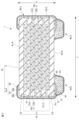
- FIG. FIG. 2 is a cross-sectional view of the multilayer ceramic capacitor 1 of the embodiment taken along line II-II in FIG. 1
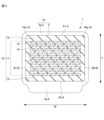
- FIG. 2 is a cross-sectional view along line III-III in FIG. 1 of the multilayer ceramic capacitor 1 of the embodiment
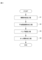
- 4 is a flow chart for explaining a method for manufacturing the multilayer ceramic capacitor 1.
- FIG. It is a figure explaining laminated body manufacturing process S1 and base electrode layer formation process S2. It is a figure explaining bump arrangement process S3 and plating layer formation process S4.
- FIG. 1 is a schematic perspective view of a laminated ceramic capacitor 1 of an embodiment.
- FIG. 2 is a cross-sectional view of the multilayer ceramic capacitor 1 of the embodiment taken along line II-II in FIG.
- FIG. 3 is a cross-sectional view along line III-III in FIG. 1 of the multilayer ceramic capacitor 1 of the embodiment.
- the multilayer ceramic capacitor 1 has a substantially rectangular parallelepiped shape, and includes a capacitor body 1A including a laminate 2 and a pair of external electrode layers 3 provided at both ends of the laminate 2, and bumps 4 attached to the capacitor body 1A. Prepare.
- the laminate 2 also includes an inner layer portion 11 including a plurality of sets of dielectric layers 14 and internal electrode layers 15 .
- the direction in which the pair of external electrode layers 3 are provided in the multilayer ceramic capacitor 1 is defined as the length direction L as a term that indicates the orientation of the multilayer ceramic capacitor 1 .
- the direction in which the dielectric layers 14 and the internal electrode layers 15 are stacked is defined as a stacking direction T.
- a direction crossing both the length direction L and the stacking direction T is defined as a width direction W.
- the width direction W is orthogonal to both the length direction L and the stacking direction T.
- FIG. 2 is a cross section passing through the center in the width direction W of the multilayer ceramic capacitor 1 and extending in the length direction L and the stacking direction T.
- a pair of outer surfaces facing in the lamination direction T are defined as a first main surface A1 and a second main surface A2
- a pair of outer surfaces facing in the width direction W are defined as a first main surface A1 and a second main surface A2.
- a pair of outer surfaces opposed to each other in the length direction L are defined as a first end surface C1 and a second end surface C2.
- the main surface A when it is not necessary to distinguish between the first main surface A1 and the second main surface A2, they are collectively referred to as the main surface A, and the first side surface B1 and the second side surface B2 need to be specifically distinguished. If not, they will be collectively referred to as the side surface B, and the first end surface C1 and the second end surface C2 will be collectively described as the end surface C unless it is necessary to distinguish them.
- the laminate 2 has rounded ridges R1 including corners.
- the ridgeline portion R1 is a portion where two surfaces of the laminate 2, that is, the main surface A and the side surface B, the main surface A and the end surface C, or the side surface B and the end surface C intersect.
- the laminate 2 includes a laminate main body 10 including an inner layer portion 11 and outer layer portions 12 arranged on both sides of the inner layer portion 11 in the lamination direction T, and side portions provided on both sides in the width direction W of the laminate main body 10. and a gap portion 16 .
- the inner layer portion 11 includes a plurality of sets of dielectric layers 14 and internal electrode layers 15 alternately laminated along the lamination direction T. As shown in FIG.
- Dielectric layer 14 is made of a ceramic material.
- the ceramic material for example, a dielectric ceramic containing BaTiO 3 as a main component is used.
- the internal electrode layers 15 include a plurality of first internal electrode layers 15a and a plurality of second internal electrode layers 15b.
- the first internal electrode layers 15a and the second internal electrode layers 15b are alternately arranged.
- the first internal electrode layer 15a includes a first facing portion 152a facing the second internal electrode layer 15b, and a first lead portion 151a drawn from the first facing portion 152a toward the first end surface C1. An end portion of the first lead-out portion 151a is exposed on the first end surface C1 and electrically connected to a first external electrode layer 3a, which will be described later.
- the second internal electrode layer 15b includes a second facing portion 152b facing the first internal electrode layer 15a, and a second lead portion 151b drawn out from the second facing portion 152b to the second end face C2. An end portion of the second lead portion 151b is electrically connected to a second external electrode layer 3b, which will be described later. Electric charges are accumulated in the first facing portion 152a of the first internal electrode layer 15a and the second facing portion 152b of the second internal electrode layer 15b.
- the internal electrode layers 15 are made of metal materials such as nickel (Ni), copper (Cu), silver (Ag), palladium (Pd), silver-palladium (Ag—Pd) alloy, and gold (Au). It is preferable that metal materials such as nickel (Ni), copper (Cu), silver (Ag), palladium (Pd), silver-palladium (Ag—Pd) alloy, and gold (Au). It is preferable that metal materials such as nickel (Ni), copper (Cu), silver (Ag), palladium (Pd), silver-palladium (Ag—Pd) alloy, and gold (Au). It is preferable that
- the outer layer portion 12 is made of the same material as the dielectric layer 14 of the inner layer portion 11 .
- the side gap portion 16 includes a first side gap portion 16a provided on the side surface B of the laminate body 10 and a second side gap portion 16b provided on the second side surface B2 side of the laminate body 10. .
- Side gap portion 16 is made of the same material as dielectric layer 14 .
- the external electrode layer 3 includes a first external electrode layer 3a provided on the first end surface C1 and a second external electrode layer 3b provided on the second end surface C2.
- the external electrode layer 3 covers not only the end surface C, but also the main surface A and part of the side surface B on the end surface C side.
- the end of the first lead-out portion 151a of the first internal electrode layer 15a is exposed on the first end surface C1 and electrically connected to the first external electrode layer 3a.
- the end of the second lead-out portion 151b of the second internal electrode layer 15b is exposed on the second end surface C2 and electrically connected to the second external electrode layer 3b.
- a plurality of capacitor elements are electrically connected in parallel between the first external electrode layer 3a and the second external electrode layer 3b.
- the external electrode layer 3 includes a base electrode layer 30 and a plating layer 32 .
- the underlying electrode layer 30 contains, for example, a conductive metal and glass G. Copper (Cu) is used as the conductive metal of the base electrode layer 30 in the embodiment.
- the plating layer 32 includes a nickel plating layer 32a arranged on the outer periphery of the base electrode layer 30 and a tin plating layer 32b arranged on the outer periphery of the nickel plating layer 32a.
- the plated layer 32 is arranged on the periphery of the bumps 4 in the portions where the bumps 4 described below are arranged.
- the bump 4 includes a pair of first bump 4a and second bump 4b.
- the first bumps 4a are arranged on one end face C1 side in the length direction L on the side of the second main surface A2, which is the board mounting surface of the capacitor body 1A, and the second bumps 4b are arranged on the other end face C2 side. It is As shown in FIG. 2, the first bump 4a and the second bump 4b are located at substantially line-symmetrical positions with respect to a center line extending in the width direction W and passing through the center in the length direction L. Distance, spaced apart.
- the bumps 4 wrap around to the second main surface A2 side and are arranged outside the capacitor body 1A with the base electrode layer 30 of the external electrode layer 3 interposed therebetween.
- the bump 4 also has a portion in direct contact with not only the base electrode layer 30 but also the outer layer portion 12 of the laminate 2 on the second main surface A2.
- Bump 4 includes copper (Cu) as a base metal and gaps 52 existing in copper (Cu). Copper Cu occupies 50% or more and 96% or less of the area of the cross section passing through the center of the bump in the width direction W and extending in the stacking direction T and the length direction L shown in FIG. In addition, about this area, a cross section is exposed, an image is imaged, and binarization processing is carried out, and it calculates by the area of copper Cu/the whole area. Confirmation of copper Cu is performed by various methods such as WDX and EDX. In an embodiment, bump 4 does not contain glass G. The bumps 4 may contain a small amount of glass G, but even in that case, the amount of glass contained in the bumps 4 is very small with respect to the base electrode layer 30 .
- the outer surface of the bump 4 has a rough surface because copper Cu grains remain undissolved.
- Nickel Ni is contained within at least 10 ⁇ m from the surface of the bump 4 .
- Nickel Ni may exist within 10 ⁇ m from the surface of the bump 4 .
- FIG. 4 is a flow chart for explaining the manufacturing method of the multilayer ceramic capacitor 1.
- the manufacturing method of the laminated ceramic capacitor 1 includes a laminate manufacturing process S1, a base electrode layer forming process S2, a bump arrangement process S3, and a plated layer forming process S4.
- FIG. 5 is a diagram for explaining the laminate manufacturing step S1 and the underlying electrode layer forming step S2.
- FIG. 6 is a diagram for explaining the bump arrangement step S3 and the plated layer formation step S4.
- Laminate manufacturing step S1 A ceramic slurry containing ceramic powder, a binder and a solvent is formed into a sheet on the periphery of a carrier film using a die coater, gravure coater, micro gravure coater, or the like to fabricate a lamination ceramic green sheet 101 that will become the dielectric layer 14 .
- a conductive paste is printed on the ceramic green sheets 101 for lamination in a belt shape by screen printing, ink jet printing, gravure printing, or the like, and conductive patterns 102 to be the internal electrode layers 15 are printed on the surfaces of the ceramic green sheets 101 for lamination.
- a printed material sheet 103 is produced.
- a plurality of conductive patterns 102 are arranged so that the conductive patterns 102 face the same direction and the conductive patterns 102 are shifted by half a pitch in the width direction between the adjacent material sheets 103.
- the material sheets 103 are stacked.
- the outer layer ceramic green sheets 112 to be the outer layer 12 are stacked on both sides of the laminated material sheet 103 .
- a plurality of stacked material sheets 103 and ceramic green sheets 112 for outer layer portions are thermocompressed to create a mother block 110 shown in FIG. 5(b).
- the mother block 110 is cut along the cutting line X shown in FIG. 5(b) and the cutting line Y intersecting the cutting line X to manufacture a plurality of laminates 2 shown in FIG. 5(c).
- the base electrode layer 30 is formed by applying and baking a conductive paste containing copper (Cu), which is a conductive metal, and glass G to the end surface C of the laminate 2 .
- the base electrode layer 30 is formed so as to extend not only to the end surfaces C on both sides of the multilayer body 2 but also to the main surface A and the side surface B of the multilayer body 2 so as to cover a part of the main surface A on the end surface C side.
- a bump manufacturing paste 44 to be used for bump manufacturing is prepared.
- the bump manufacturing paste is a conductive paste.
- the bump manufacturing paste 44 contains copper Cu powder, an epoxy resin, and a solvent.
- the bump manufacturing paste 44 does not contain a curing agent such as phenolic resin or imidazole.
- the volume ratio of copper to the epoxy resin is 70% or more and 90% or less.
- the epoxy resin is a bisphenol A type epoxy resin.
- the conductive paste Cu contains copper Cu powder with a median diameter d50 of 5 ⁇ m or more and 10 ⁇ m or less in a volume ratio of 55% or more and 95% or less with respect to copper Cu powder with a median diameter d50 of 0.5 ⁇ m or more and 1.5 ⁇ m or less.
- the solvent is, for example, diethylene glycol monobutyl ether, diethylene glycol monoethyl ether or diethylene glycol monomethyl ether.
- a holding substrate 40 as shown in FIG. 6 is used for forming the bumps 4, for example, a holding substrate 40 as shown in FIG. 6 is used. As shown in FIG. 6A, a bump manufacturing paste 44 is placed on a holding substrate 40 by screen printing, dispensing, or the like. It should be noted that the holding substrate 40 is preferably made of a member that can withstand the baking temperature of Cu.
- the capacitor body 1A is mounted on the outer circumference of the holding substrate 40 with the second main surface A2 facing the holding substrate 40. As shown in FIG. At this time, the external electrode layer 3 of the capacitor body 1A and the bump manufacturing paste 44 are aligned, and the bump manufacturing paste 44 adheres to the capacitor body 1A.
- a heating process is carried out to heat at a temperature at which copper Cu is seized.
- the metal in the paste forms an intermetallic compound and hardens to form bumps 4 bonded to capacitor main body 1A and external electrode layer 3 .
- an alloy may be formed in the sintered body. Examples of the plurality of metals include copper Cu and nickel Ni.
- the capacitor body 1A is separated from the holding substrate 40 together with the bumps 4, resulting in the state shown in FIG. 6(c).
- a nickel plating layer 32a is formed on the portion of the capacitor body 1A where the base electrode layer 30 is exposed and on the periphery of the bump 4, and a tin plating layer 32b is formed on the periphery of the nickel plating layer 32a.
- the laminated ceramic capacitor 1 is manufactured through the above steps.
- the bump 4 contains copper (Cu), and the copper (Cu) occupies an area of 50% or more and 96% or less in a cross section passing through the center of the bump 4 in the width direction W and extending in the stacking direction T and the length direction L.
- the external electrode layer 3 includes a base electrode layer 30 containing copper (Cu) and glass (G). Since the base electrode layer 30 and the bumps 4 are both formed by sintering a conductive paste containing copper (Cu), the bond between the base electrode layer 30 and the bumps 4 is strong and has an adhesive strength. improves.
- the multilayer ceramic capacitor 1 can be firmly attached to the mounting board using solder. can be done.
- the bump manufacturing paste 44 contains copper Cu powder, epoxy resin, and solvent, and does not contain a curing agent such as phenolic resin or imidazole. Since the bump manufacturing paste 44 does not contain a hardening agent, it is possible to strengthen the bond between the copper-Cu powders. Thereby, the strength of the bump 4 is improved.
- the volume ratio of copper (Cu) to epoxy resin in the bump manufacturing paste 44 is 70% or more and 90% or less. Since the volume ratio of copper Cu is large, it has good electrical conductivity.
- the metal contained in the underlying electrode layer 30 may not be copper (Cu).
- the base electrode layer 30 may be formed by sintering a conductive paste containing a metal such as nickel Ni.
- the metal contained in the external electrode layer 3 is nickel Ni
- the Ni contained in the base electrode layer 30 and the Cu contained in the bump 4 are alloyed to form the sintered portion 51 .
- the sintered portion 51 is not formed, if both the base electrode layer 30 and the bump 4 are formed by sintering a conductive paste containing a metal, the gap between the base electrode layer 30 and the bump 4 can be reduced. The bond becomes stronger and the adhesive strength improves.
Landscapes
- Engineering & Computer Science (AREA)
- Power Engineering (AREA)
- Microelectronics & Electronic Packaging (AREA)
- Manufacturing & Machinery (AREA)
- Chemical & Material Sciences (AREA)
- Ceramic Engineering (AREA)
- Inorganic Chemistry (AREA)
- Materials Engineering (AREA)
- Ceramic Capacitors (AREA)
- Fixed Capacitors And Capacitor Manufacturing Machines (AREA)
Abstract
コンデンサ本体とバンプとの間の接着力が向上された積層セラミックコンデンサ及びバンプ製造用ペーストを提供する。本発明の積層セラミックコンデンサ1は、誘電体層14と内部電極層15とが交互に積層された積層体2と、積層体2における、長さ方向の両端に設けられた2つの端面のそれぞれに配置され、積層体の積層方向の両端に設けられた2つの主面の端面側、及び、幅方向の両端に設けられた2つの側面の端面側を覆い、且つ内部電極層と接続する外部電極層3と、積層体2の2つの主面のうちの一方における、2つの端面側のそれぞれに、主面側を覆う外部電極層を挟んで配置されたバンプ4と、を備え、バンプ4は、バンプ4の幅方向の中央を通り且つ積層方向と長さ方向とに延びる断面において、50%以上96%以下の面積を占める銅Cuを含む。
Description
本発明は、積層セラミックコンデンサ及びバンプ製造用ペーストに関する。
積層セラミックコンデンサは、誘電体層と内部電極とが交互に積み重ねられた内層部を有する。そして、その内層部の上部と下部とに外層部としての誘電体層が配置されて直方体状の積層体が形成され、積層体の長手方向の両端面に外部電極が設けられてコンデンサ本体が形成される。
さらに、いわゆる「鳴き」の発生を抑制するために、コンデンサ本体における基板に実装される側に外部電極の一部を覆うように形成されたバンプを備える積層セラミックコンデンサが知られている(特許文献1参照)。
さらに、いわゆる「鳴き」の発生を抑制するために、コンデンサ本体における基板に実装される側に外部電極の一部を覆うように形成されたバンプを備える積層セラミックコンデンサが知られている(特許文献1参照)。
しかし、従来、コンデンサ本体とバンプとの間の接着力が弱く、バンプがコンデンサ本体から剥がれてしまう場合があった。
本発明は、コンデンサ本体とバンプとの間の接着力が向上された積層セラミックコンデンサ及びバンプ製造用ペーストを提供することを目的とする。
上記課題を解決するために本発明は、誘電体層と内部電極層とが交互に積層された積層体と、前記積層体における、積層方向と交差する長さ方向の両端に設けられた2つの端面のそれぞれに配置され、前記積層体の前記積層方向の両端に設けられた2つの主面の端面側、及び、前記積層方向及び前記長さ方向と交差する幅方向の両端に設けられた2つの側面の前記端面側を覆い、且つ前記内部電極層と接続する外部電極層と、前記積層体の2つの前記主面のうちの一方における、2つの前記端面側のそれぞれに、前記主面側を覆う前記外部電極層を挟んで配置されたバンプと、を備え、前記バンプは、前記バンプの前記幅方向の中央を通り且つ前記積層方向と前記長さ方向とに延びる断面において、50%以上96%以下の面積を占める銅を含む、積層セラミックコンデンサを提供する。
また、上記課題を解決するために本発明は、銅紛と、エポキシ樹脂と、溶剤と、を含み、フェノール樹脂やイミダゾールなどの硬化剤を含まない、上積層セラミックコンデンサの、バンプ製造用ペーストを提供する。
本発明によれば、コンデンサ本体とバンプとの間の接着力が向上された積層セラミックコンデンサ及びバンプ製造用ペーストを提供することができる。
本発明の実施形態にかかる積層セラミックコンデンサ1について説明する。図1は、実施形態の積層セラミックコンデンサ1の概略斜視図である。図2は、実施形態の積層セラミックコンデンサ1の図1におけるII-II線に沿った断面図である。図3は、実施形態の積層セラミックコンデンサ1の図1におけるIII-III線に沿った断面図である。
積層セラミックコンデンサ1は、略直方体形状で、積層体2及び積層体2の両端に設けられた一対の外部電極層3とを備えるコンデンサ本体1Aと、コンデンサ本体1Aに取り付けられたバンプ4と、を備える。また、積層体2は、誘電体層14と内部電極層15とを複数組含む内層部11を含む。
以下の説明において、積層セラミックコンデンサ1の向きを表わす用語として、積層セラミックコンデンサ1において、一対の外部電極層3が設けられている方向を長さ方向Lとする。誘電体層14と内部電極層15とが積層されている方向を積層方向Tとする。長さ方向L及び積層方向Tのいずれにも交差する方向を幅方向Wとする。なお、実施形態においては、幅方向Wは長さ方向L及び積層方向Tのいずれにも直交している。
図2は、積層セラミックコンデンサ1の幅方向Wの中央を通り、且つ長さ方向Lと積層方向Tに延びる断面である。
図2は、積層セラミックコンデンサ1の幅方向Wの中央を通り、且つ長さ方向Lと積層方向Tに延びる断面である。
(積層体2の外表面)
また、積層体2の6つの外表面のうち、積層方向Tに相対する一対の外表面を第1主面A1と第2主面A2とし、幅方向Wに相対する一対の外表面を第1側面B1と第2側面B2とし、長さ方向Lに相対する一対の外表面を第1端面C1と第2端面C2とする。なお、第1主面A1と第2主面A2とを特に区別して説明する必要のない場合、まとめて主面Aとし、第1側面B1と第2側面B2とを特に区別して説明する必要のない場合、まとめて側面Bとし、第1端面C1と第2端面C2とを特に区別して説明する必要のない場合、まとめて端面Cとして説明する。
また、積層体2の6つの外表面のうち、積層方向Tに相対する一対の外表面を第1主面A1と第2主面A2とし、幅方向Wに相対する一対の外表面を第1側面B1と第2側面B2とし、長さ方向Lに相対する一対の外表面を第1端面C1と第2端面C2とする。なお、第1主面A1と第2主面A2とを特に区別して説明する必要のない場合、まとめて主面Aとし、第1側面B1と第2側面B2とを特に区別して説明する必要のない場合、まとめて側面Bとし、第1端面C1と第2端面C2とを特に区別して説明する必要のない場合、まとめて端面Cとして説明する。
積層体2は、角部を含む稜線部R1に丸みがつけられていることが好ましい。稜線部R1は、積層体2の2面、すなわち主面Aと側面B、主面Aと端面C、又は、側面Bと端面Cが交わる部分である。
(積層体2)
積層体2は、内層部11と、内層部11の積層方向T両側にそれぞれ配置される外層部12とを備える積層体本体10と、積層体本体10の幅方向Wの両側に設けられたサイドギャップ部16とを備える。
積層体2は、内層部11と、内層部11の積層方向T両側にそれぞれ配置される外層部12とを備える積層体本体10と、積層体本体10の幅方向Wの両側に設けられたサイドギャップ部16とを備える。
(内層部11)
内層部11は、積層方向Tに沿って交互に積層された誘電体層14と内部電極層15とを複数組含む。
内層部11は、積層方向Tに沿って交互に積層された誘電体層14と内部電極層15とを複数組含む。
誘電体層14は、セラミック材料で製造されている。セラミック材料としては、例えば、BaTiO3を主成分とする誘電体セラミックが用いられる。
内部電極層15は、複数の第1内部電極層15aと、複数の第2内部電極層15bとを備える。第1内部電極層15aと第2内部電極層15bとは、交互に配置されている。第1内部電極層15aは、第2内部電極層15bと対向する第1対向部152aと、第1対向部152aから第1端面C1側に引き出された第1引き出し部151aとを備える。第1引き出し部151aの端部は、第1端面C1に露出し、後述の第1外部電極層3aに電気的に接続されている。第2内部電極層15bは、第1内部電極層15aと対向する第2対向部152bと、第2対向部152bから第2端面C2に引き出された第2引き出し部151bとを備える。第2引き出し部151bの端部は、後述の第2外部電極層3bに電気的に接続されている。第1内部電極層15aの第1対向部152aと、第2内部電極層15bの第2対向部152bとに電荷が蓄積される。
内部電極層15は、例えばニッケル(Ni)、銅(Cu)、銀(Ag)、パラジウム(Pd)、銀-パラジウム(Ag-Pd)合金、金(Au)等に代表される金属材料により形成されていることが好ましい。
(外層部12)
外層部12は、内層部11の誘電体層14と同じ材料で製造されている。
外層部12は、内層部11の誘電体層14と同じ材料で製造されている。
(サイドギャップ部16)
サイドギャップ部16は、積層体本体10の側面B側に設けられた第1サイドギャップ部16aと、積層体本体10の第2側面B2側に設けられた第2サイドギャップ部16bと、を備える。サイドギャップ部16は、誘電体層14と同様の材料で製造されている。
サイドギャップ部16は、積層体本体10の側面B側に設けられた第1サイドギャップ部16aと、積層体本体10の第2側面B2側に設けられた第2サイドギャップ部16bと、を備える。サイドギャップ部16は、誘電体層14と同様の材料で製造されている。
(外部電極層3)
外部電極層3は、第1端面C1に設けられた第1外部電極層3aと、第2端面C2に設けられた第2外部電極層3bとを備える。外部電極層3は、端面Cだけでなく、主面A及び側面Bの端面C側の一部も覆っている。
外部電極層3は、第1端面C1に設けられた第1外部電極層3aと、第2端面C2に設けられた第2外部電極層3bとを備える。外部電極層3は、端面Cだけでなく、主面A及び側面Bの端面C側の一部も覆っている。
上述のように、第1内部電極層15aの第1引き出し部151aの端部は第1端面C1に露出し、第1外部電極層3aに電気的に接続されている。また、第2内部電極層15bの第2引き出し部151bの端部は第2端面C2に露出し、第2外部電極層3bに電気的に接続されている。これにより、第1外部電極層3aと第2外部電極層3bとの間は、複数のコンデンサ要素が電気的に並列に接続された構造となっている。
また、外部電極層3は、下地電極層30とめっき層32とを含む。
下地電極層30は、例えば、導電性金属とガラスGとを含む。下地電極層30の導電性金属は、実施形態では銅Cuが用いられる。
めっき層32は、下地電極層30の外周に配置されたニッケルめっき層32a、及びニッケルめっき層32aの外周に配置された錫めっき層32bを含む。ただし、めっき層32は、次に説明するバンプ4が配置されている部分においては、バンプ4の外周に配置されている。
(バンプ4)
バンプ4は、一対の第1バンプ4aと第2バンプ4bとを備える。第1バンプ4aは、コンデンサ本体1Aの基板実装面である第2主面A2側における、長さ方向Lの一方の端面C1側に配置され、第2バンプ4bは、他方の端面C2側に配置されている。第1バンプ4aと第2バンプ4bとは、図2に示すように長さ方向Lの中心を通り幅方向Wに延びる中央線を挟んで略線対称の位置に、長さ方向Lに一定の距離、離間して配置されている。
バンプ4は、一対の第1バンプ4aと第2バンプ4bとを備える。第1バンプ4aは、コンデンサ本体1Aの基板実装面である第2主面A2側における、長さ方向Lの一方の端面C1側に配置され、第2バンプ4bは、他方の端面C2側に配置されている。第1バンプ4aと第2バンプ4bとは、図2に示すように長さ方向Lの中心を通り幅方向Wに延びる中央線を挟んで略線対称の位置に、長さ方向Lに一定の距離、離間して配置されている。
バンプ4は、第2主面A2側まで回り込んで、外部電極層3の下地電極層30を挟んでコンデンサ本体1Aの外側に配置されている。また、バンプ4は、第2主面A2において、下地電極層30だけでなく、積層体2の外層部12の部分と直接接触している部分も有する。
バンプ4は、ベース金属として銅Cuと、銅Cu内に存在する隙間52とを含む。銅Cuは、図2に示すバンプの幅方向Wの中央を通り且つ積層方向Tと長さ方向Lとに延びる断面において、50%以上96%以下の面積を占める。なお、この面積については、断面を露出させ、撮像し、2値化処理することで、銅Cuの面積/全体の面積で算出される。銅Cuであることの確認は、WDX、EDXなど種々の方法で行われる。
実施形態において、バンプ4はガラスGを含まない。バンプ4は、わずかにガラスGを含んでいてもよいが、その場合も、バンプ4に含まれるガラスは、下地電極層30に対して微量である。
実施形態において、バンプ4はガラスGを含まない。バンプ4は、わずかにガラスGを含んでいてもよいが、その場合も、バンプ4に含まれるガラスは、下地電極層30に対して微量である。
バンプ4の外面は、図示しないが、銅Cuの粒が完全に溶けずに残っていて、表面が荒くなっている。また、バンプ4の表面から少なくとも10μm以内に、ニッケルNiが含まれている。ニッケルNiは、バンプ4の表面から10μmより内部に存在していてもよい。
(積層セラミックコンデンサ1の製造方法)
図4は、積層セラミックコンデンサ1の製造方法を説明するフローチャートである。積層セラミックコンデンサ1の製造方法は、積層体製造工程S1と、下地電極層形成工程S2と、バンプ配置工程S3と、めっき層形成工程S4とを含む。図5は、積層体製造工程S1と、下地電極層形成工程S2と、を説明する図である。図6はバンプ配置工程S3と、めっき層形成工程S4とを説明する図である。
図4は、積層セラミックコンデンサ1の製造方法を説明するフローチャートである。積層セラミックコンデンサ1の製造方法は、積層体製造工程S1と、下地電極層形成工程S2と、バンプ配置工程S3と、めっき層形成工程S4とを含む。図5は、積層体製造工程S1と、下地電極層形成工程S2と、を説明する図である。図6はバンプ配置工程S3と、めっき層形成工程S4とを説明する図である。
(積層体製造工程S1)
セラミックス粉末、バインダ及び溶剤を含むセラミックスラリーをキャリアフィルムの外周においてダイコータ、グラビアコータ、マイクログラビアコータ等を用いてシート状に成形して誘電体層14となる積層用セラミックグリーンシート101を製作する。次いで、積層用セラミックグリーンシート101に導電体ペーストをスクリーン印刷、インクジェット印刷、グラビア印刷等によって帯状に印刷し、積層用セラミックグリーンシート101の表面に内部電極層15となる導電パターン102を印刷するが印刷された素材シート103を製作する。
セラミックス粉末、バインダ及び溶剤を含むセラミックスラリーをキャリアフィルムの外周においてダイコータ、グラビアコータ、マイクログラビアコータ等を用いてシート状に成形して誘電体層14となる積層用セラミックグリーンシート101を製作する。次いで、積層用セラミックグリーンシート101に導電体ペーストをスクリーン印刷、インクジェット印刷、グラビア印刷等によって帯状に印刷し、積層用セラミックグリーンシート101の表面に内部電極層15となる導電パターン102を印刷するが印刷された素材シート103を製作する。
続いて、図5(a)に示すように、導電パターン102が同一の方向を向き且つ導電パターン102が隣り合う素材シート103間において幅方向において半ピッチずつずれた状態になるように、複数の素材シート103を積み重ねる。さらに、複数枚積層された素材シート103の両側にそれぞれ、外層部12となる外層部用セラミックグリーンシート112を積み重ねる。
積み重ねた複数の素材シート103と外層部用セラミックグリーンシート112とを熱圧着し、図5(b)に示すマザーブロック110を作成する。
次いで、マザーブロック110を、図5(b)に示す切断線X及び切断線Xと交差する切断線Yに沿って切断し、図5(c)に示す積層体2を複数製造する。
(下地電極層形成工程S2)
続いて、積層体2の端面Cに、導電性金属である銅CuとガラスGとを含む導電性ペーストを塗布、焼き付けることにより下地電極層30を形成する。下地電極層30は、積層体2両側の端面Cのみならず、積層体2の主面A及び側面B側まで延びて、主面Aの端面C側の一部も覆うように形成する。
続いて、積層体2の端面Cに、導電性金属である銅CuとガラスGとを含む導電性ペーストを塗布、焼き付けることにより下地電極層30を形成する。下地電極層30は、積層体2両側の端面Cのみならず、積層体2の主面A及び側面B側まで延びて、主面Aの端面C側の一部も覆うように形成する。
(バンプ配置工程S3)
バンプ製造に用いる、バンプ製造用ペースト44を用意する。バンプ製造用ペーストは導電性ペーストである。
バンプ製造用ペースト44は、銅Cu紛と、エポキシ樹脂と、溶剤と、を含む。そしてバンプ製造用ペースト44は、フェノール樹脂やイミダゾールなどの硬化剤を含まない。
バンプ製造に用いる、バンプ製造用ペースト44を用意する。バンプ製造用ペーストは導電性ペーストである。
バンプ製造用ペースト44は、銅Cu紛と、エポキシ樹脂と、溶剤と、を含む。そしてバンプ製造用ペースト44は、フェノール樹脂やイミダゾールなどの硬化剤を含まない。
エポキシ樹脂に対する銅の体積比率は70%以上90%以下である。エポキシ樹脂は、ビスフェノールA型エポキシ樹脂である。
導電性ペーストCuは、メジアン径d50が5μm以上10μm以下の銅Cu粉を、メジアン径d50が0.5μm以上1.5μm以下の銅Cu粉に対して、体積比率55%以上95%以下含む。
溶剤は、例えばジエチレングリコールモノブチルエーテル、ジエチレングリコールモノエチルエーテル又はジエチレングリコールモノメチルエーテルである。
バンプ4の形成には、例えば図6に示すような保持基板40を用いる。図6(a)に示すように保持基板40の上に、バンプ製造用ペースト44をスクリーン印刷法又はディスペンス法等により配置する。なお、保持基板40は、Cuの焼き付け温度に耐えられる部材が好ましい。
次に、コンデンサ本体1Aを図6(b)に示すように、第2主面A2側が保持基板40に対向する姿勢で保持基板40の外周に搭載する。このとき、コンデンサ本体1Aの外部電極層3とバンプ製造用ペースト44とが位置合わせされ、バンプ製造用ペースト44がコンデンサ本体1Aに付着する。
この状態で、銅Cuが焼き付く温度で加熱する加熱工程を実施する。これにより、ペースト中の金属が金属間化合物を生成するとともに、硬化し、コンデンサ本体1Aならびに外部電極層3に接合した状態のバンプ4が形成される。なお、複数の金属が入った場合は、焼結体内で合金を生成する場合があり、複数の金属としては、例えば銅CuとニッケルNiなどがあげられる。
その後、コンデンサ本体1Aがバンプ4とともに、保持基板40から分離され、図6(c)の状態となる。
(めっき層形成工程S4)
次いで、コンデンサ本体1Aにおける下地電極層30が露出している部分及びバンプ4の外周に、ニッケルめっき層32aを形成し、さらにニッケルめっき層32aの外周に錫めっき層32bとを形成する。以上の工程により積層セラミックコンデンサ1が製造される。
次いで、コンデンサ本体1Aにおける下地電極層30が露出している部分及びバンプ4の外周に、ニッケルめっき層32aを形成し、さらにニッケルめっき層32aの外周に錫めっき層32bとを形成する。以上の工程により積層セラミックコンデンサ1が製造される。
(実施形態の効果)
バンプ4は銅Cuを含み、銅Cuは、バンプ4の幅方向Wの中央を通り且つ積層方向Tと長さ方向Lとに延びる断面において、50%以上96%以下の面積を占める。そして、外部電極層3は、銅CuとガラスGとを含む下地電極層30を含む。下地電極層30とバンプ4は、共に銅Cuが含まれる導電ペーストが焼結されることによって形成されたものであるため、下地電極層30とバンプ4との間の結合が強硬になり接着力が向上する。
バンプ4は銅Cuを含み、銅Cuは、バンプ4の幅方向Wの中央を通り且つ積層方向Tと長さ方向Lとに延びる断面において、50%以上96%以下の面積を占める。そして、外部電極層3は、銅CuとガラスGとを含む下地電極層30を含む。下地電極層30とバンプ4は、共に銅Cuが含まれる導電ペーストが焼結されることによって形成されたものであるため、下地電極層30とバンプ4との間の結合が強硬になり接着力が向上する。
外部電極層3及びバンプ4の外周に、ニッケルめっき32aと、ニッケルめっき32の外周に配置された錫めっき32bと、を備えるので、積層セラミックコンデンサ1をはんだを用いて実装基板に強固に取り付けることができる。
バンプ製造用ペースト44は、銅Cu紛と、エポキシ樹脂と、溶剤と、を含み、フェノール樹脂やイミダゾールなどの硬化剤を含まない。バンプ製造用ペースト44は硬化剤を含まないので、銅Cu粉同士の結合を強くすることができる。これにより、バンプ4としての強度が向上する。
バンプ製造用ペースト44におけるエポキシ樹脂に対する銅Cuの体積比率は、70%以上90%以下である。銅Cuの体積比率が大きいので、良好な導電性を有する。
(変形形態)
以上、本発明の実施形態について説明したが、本発明はこれに限定されず、発明の範囲内において種々の変形が可能である。
以上、本発明の実施形態について説明したが、本発明はこれに限定されず、発明の範囲内において種々の変形が可能である。
例えば、下地電極層30に含まれる金属は銅Cuでなくてもよい。例えば、下地電極層30は、ニッケルNi等の金属が含まれる導電性ペーストが焼結されることによって形成されたものであってもよい。外部電極層3に含まれる金属がニッケルNiの場合、下地電極層30に含まれるNiとバンプ4に含まれるCuとが合金化し焼結部51を形成する。
なお、焼結部51が形成されなくても、下地電極層30とバンプ4が共に金属が含まれる導電性ペーストが焼結されたものであれば、下地電極層30とバンプ4との間の結合が強硬になり接着力が向上する。
なお、焼結部51が形成されなくても、下地電極層30とバンプ4が共に金属が含まれる導電性ペーストが焼結されたものであれば、下地電極層30とバンプ4との間の結合が強硬になり接着力が向上する。
Cu 銅
G ガラス
Ni ニッケル
1 積層セラミックコンデンサ
1A コンデンサ本体
2 積層体
3 外部電極層
4 バンプ
10 積層体本体
11 内層部
12 外層部
14 誘電体層
15 内部電極層
30 下地電極層
32 めっき層
32a ニッケルめっき層
32b 錫めっき層
44 バンプ製造用ペースト
51 焼結部
G ガラス
Ni ニッケル
1 積層セラミックコンデンサ
1A コンデンサ本体
2 積層体
3 外部電極層
4 バンプ
10 積層体本体
11 内層部
12 外層部
14 誘電体層
15 内部電極層
30 下地電極層
32 めっき層
32a ニッケルめっき層
32b 錫めっき層
44 バンプ製造用ペースト
51 焼結部
Claims (11)
- 誘電体層と内部電極層とが交互に積層された積層体と、
前記積層体における、積層方向と交差する長さ方向の両端に設けられた2つの端面のそれぞれに配置され、前記積層体の前記積層方向の両端に設けられた2つの主面の端面側、及び、前記積層方向及び前記長さ方向と交差する幅方向の両端に設けられた2つの側面の前記端面側を覆い、且つ前記内部電極層と接続する外部電極層と、
前記積層体の2つの前記主面のうちの一方における、2つの前記端面側のそれぞれに、前記主面側を覆う前記外部電極層を挟んで配置されたバンプと、を備え、
前記バンプは、前記バンプの前記幅方向の中央を通り且つ前記積層方向と前記長さ方向とに延びる断面において、50%以上96%以下の面積を占める銅を含む、
積層セラミックコンデンサ。 - 前記バンプの表面から少なくとも10μm以内に、ニッケルが含まれている、
請求項1に記載の積層セラミックコンデンサ。 - 前記外部電極層は、銅とガラスとを含む下地電極層を含み、
前記下地電極層と前記バンプに含まれる前記銅とが、導通している、
請求項1又は請求項2に記載の積層セラミックコンデンサ。 - 前記バンプは,前記下地電極層よりも前記ガラスの含有量が少ない、
請求項3に記載の積層セラミックコンデンサ。 - 前記外部電極層及び前記バンプの外周に、
ニッケルめっきと、
前記ニッケルめっきの外周に配置された錫めっきと、を備える、
請求項1から請求項4のいずれか1項に記載の積層セラミックコンデンサ。 - 前記バンプは、前記積層体に直接取り付けられている部分を有する、
る請求項1から請求項4のいずれか1項に記載の積層セラミックコンデンサ。 - 銅紛と、
エポキシ樹脂と、
溶剤と、を含み、
フェノール樹脂やイミダゾールなどの硬化剤を含まない、
請求項1から請求項6のいずれか1項に記載の積層セラミックコンデンサの、バンプ製造用ペースト。 - 前記エポキシ樹脂に対する前記銅の体積比率は、70%以上90%以下である、
請求項7に記載のバンプ製造用ペースト。 - 前記エポキシ樹脂は、ビスフェノールA型エポキシ樹脂である、
請求項7又は請求項8に記載のバンプ製造用ペースト。 - メジアン径d50が5μm以上10μm以下の銅粉を、メジアン径d50が0.5μm以上1.5μm以下の銅粉に対して、体積比率55%以上95%以下含む、
請求項7から請求項9のいずれか1項に記載のバンプ製造用ペースト。 - 前記溶剤がジエチレングリコールモノブチルエーテル、又はジエチレングリコールモノエチルエーテルである、
請求項7から請求項10のいずれか1項に記載のバンプ製造用ペースト。
Priority Applications (2)
| Application Number | Priority Date | Filing Date | Title |
|---|---|---|---|
| JP2023559638A JPWO2023085264A5 (ja) | 2022-11-08 | 積層セラミックコンデンサ及び積層セラミックコンデンサのバンプ製造用ペースト | |
| US18/629,028 US12469644B2 (en) | 2021-11-10 | 2024-04-08 | Multilayer ceramic capacitor and bump-producing paste |
Applications Claiming Priority (2)
| Application Number | Priority Date | Filing Date | Title |
|---|---|---|---|
| JP2021183734 | 2021-11-10 | ||
| JP2021-183734 | 2021-11-10 |
Related Child Applications (1)
| Application Number | Title | Priority Date | Filing Date |
|---|---|---|---|
| US18/629,028 Continuation US12469644B2 (en) | 2021-11-10 | 2024-04-08 | Multilayer ceramic capacitor and bump-producing paste |
Publications (1)
| Publication Number | Publication Date |
|---|---|
| WO2023085264A1 true WO2023085264A1 (ja) | 2023-05-19 |
Family
ID=86335743
Family Applications (1)
| Application Number | Title | Priority Date | Filing Date |
|---|---|---|---|
| PCT/JP2022/041548 Ceased WO2023085264A1 (ja) | 2021-11-10 | 2022-11-08 | 積層セラミックコンデンサ及びバンプ製造用ペースト |
Country Status (2)
| Country | Link |
|---|---|
| US (1) | US12469644B2 (ja) |
| WO (1) | WO2023085264A1 (ja) |
Cited By (1)
| Publication number | Priority date | Publication date | Assignee | Title |
|---|---|---|---|---|
| JPWO2025115525A1 (ja) * | 2023-12-01 | 2025-06-05 |
Citations (6)
| Publication number | Priority date | Publication date | Assignee | Title |
|---|---|---|---|---|
| JP2010108845A (ja) * | 2008-10-31 | 2010-05-13 | Namics Corp | 外部電極用導電性ペースト、及びそれを用いて形成した外部電極を備えた積層セラミック電子部品 |
| WO2018101405A1 (ja) * | 2016-12-01 | 2018-06-07 | 株式会社村田製作所 | チップ型電子部品 |
| JP2019050278A (ja) * | 2017-09-08 | 2019-03-28 | Tdk株式会社 | 電子部品及び電子部品装置 |
| US10566137B2 (en) * | 2017-10-02 | 2020-02-18 | Samsung Electro-Mechanics Co., Ltd. | Multilayer electronic component and board having the same |
| JP2020181962A (ja) * | 2019-04-26 | 2020-11-05 | 株式会社村田製作所 | チップ型電子部品および電子部品の実装構造体 |
| JP2021027054A (ja) * | 2019-07-31 | 2021-02-22 | 株式会社村田製作所 | チップ型電子部品、電子部品の実装構造体および電子部品連 |
Family Cites Families (4)
| Publication number | Priority date | Publication date | Assignee | Title |
|---|---|---|---|---|
| KR20120060868A (ko) * | 2010-09-29 | 2012-06-12 | 쿄세라 코포레이션 | 콘덴서 |
| KR101983154B1 (ko) * | 2013-11-05 | 2019-05-28 | 삼성전기주식회사 | 적층 세라믹 커패시터 |
| KR101630037B1 (ko) | 2014-05-08 | 2016-06-13 | 삼성전기주식회사 | 적층 세라믹 커패시터, 어레이형 적층 세라믹 커패시터, 그 제조 방법 및 그 실장 기판 |
| WO2020040138A1 (ja) * | 2018-08-23 | 2020-02-27 | 昭栄化学工業株式会社 | 導電性ペースト |
-
2022
- 2022-11-08 WO PCT/JP2022/041548 patent/WO2023085264A1/ja not_active Ceased
-
2024
- 2024-04-08 US US18/629,028 patent/US12469644B2/en active Active
Patent Citations (6)
| Publication number | Priority date | Publication date | Assignee | Title |
|---|---|---|---|---|
| JP2010108845A (ja) * | 2008-10-31 | 2010-05-13 | Namics Corp | 外部電極用導電性ペースト、及びそれを用いて形成した外部電極を備えた積層セラミック電子部品 |
| WO2018101405A1 (ja) * | 2016-12-01 | 2018-06-07 | 株式会社村田製作所 | チップ型電子部品 |
| JP2019050278A (ja) * | 2017-09-08 | 2019-03-28 | Tdk株式会社 | 電子部品及び電子部品装置 |
| US10566137B2 (en) * | 2017-10-02 | 2020-02-18 | Samsung Electro-Mechanics Co., Ltd. | Multilayer electronic component and board having the same |
| JP2020181962A (ja) * | 2019-04-26 | 2020-11-05 | 株式会社村田製作所 | チップ型電子部品および電子部品の実装構造体 |
| JP2021027054A (ja) * | 2019-07-31 | 2021-02-22 | 株式会社村田製作所 | チップ型電子部品、電子部品の実装構造体および電子部品連 |
Cited By (3)
| Publication number | Priority date | Publication date | Assignee | Title |
|---|---|---|---|---|
| JPWO2025115525A1 (ja) * | 2023-12-01 | 2025-06-05 | ||
| WO2025115525A1 (ja) * | 2023-12-01 | 2025-06-05 | 京セラ株式会社 | 積層型電子部品 |
| US12603230B2 (en) | 2023-12-01 | 2026-04-14 | Kyocera Corporation | Multilayer electronic component |
Also Published As
| Publication number | Publication date |
|---|---|
| US20240258037A1 (en) | 2024-08-01 |
| US12469644B2 (en) | 2025-11-11 |
| JPWO2023085264A1 (ja) | 2023-05-19 |
Similar Documents
| Publication | Publication Date | Title |
|---|---|---|
| US20250218658A1 (en) | Multilayer ceramic capacitor and method of manufacturing multilayer ceramic capacitor | |
| US12597564B2 (en) | Multilayer ceramic capacitor and paste for producing bump | |
| US12237111B2 (en) | Multilayer ceramic capacitor | |
| US12469644B2 (en) | Multilayer ceramic capacitor and bump-producing paste | |
| US20240258029A1 (en) | Multilayer ceramic capacitor and bump-producing paste | |
| JP5769487B2 (ja) | コンデンサ | |
| KR20250121127A (ko) | 적층 세라믹 전자부품 | |
| TWI436389B (zh) | Electronic Parts | |
| CN115938797A (zh) | 层叠陶瓷电子部件 | |
| US20260058062A1 (en) | Multilayer ceramic electronic component | |
| US20260018337A1 (en) | Multilayer ceramic electronic component | |
| US20260011504A1 (en) | Multilayer ceramic electronic component | |
| US20260018340A1 (en) | Multilayer ceramic electronic component | |
| US20260011502A1 (en) | Laminated ceramic electronic component | |
| WO2025163971A1 (ja) | 積層セラミック電子部品 | |
| WO2025163972A1 (ja) | 積層セラミック電子部品 | |
| WO2025163973A1 (ja) | 積層セラミック電子部品 | |
| KR101508838B1 (ko) | 다층 세라믹 소자 및 이를 구비하는 실장 구조물 | |
| WO2025046970A1 (ja) | 積層セラミック電子部品 | |
| WO2024203711A1 (ja) | 積層セラミック電子部品 |
Legal Events
| Date | Code | Title | Description |
|---|---|---|---|
| 121 | Ep: the epo has been informed by wipo that ep was designated in this application |
Ref document number: 22892762 Country of ref document: EP Kind code of ref document: A1 |
|
| ENP | Entry into the national phase |
Ref document number: 2023559638 Country of ref document: JP Kind code of ref document: A |
|
| NENP | Non-entry into the national phase |
Ref country code: DE |
|
| 122 | Ep: pct application non-entry in european phase |
Ref document number: 22892762 Country of ref document: EP Kind code of ref document: A1 |