WO2023084858A1 - 電子部品 - Google Patents
電子部品 Download PDFInfo
- Publication number
- WO2023084858A1 WO2023084858A1 PCT/JP2022/030676 JP2022030676W WO2023084858A1 WO 2023084858 A1 WO2023084858 A1 WO 2023084858A1 JP 2022030676 W JP2022030676 W JP 2022030676W WO 2023084858 A1 WO2023084858 A1 WO 2023084858A1
- Authority
- WO
- WIPO (PCT)
- Prior art keywords
- recess
- electronic component
- glass film
- electrode
- external electrode
- Prior art date
- Legal status (The legal status is an assumption and is not a legal conclusion. Google has not performed a legal analysis and makes no representation as to the accuracy of the status listed.)
- Ceased
Links
Images


Classifications
-
- H—ELECTRICITY
- H01—ELECTRIC ELEMENTS
- H01C—RESISTORS
- H01C7/00—Non-adjustable resistors formed as one or more layers or coatings; Non-adjustable resistors made from powdered conducting material or powdered semi-conducting material with or without insulating material
- H01C7/04—Non-adjustable resistors formed as one or more layers or coatings; Non-adjustable resistors made from powdered conducting material or powdered semi-conducting material with or without insulating material having negative temperature coefficient
-
- H—ELECTRICITY
- H01—ELECTRIC ELEMENTS
- H01C—RESISTORS
- H01C7/00—Non-adjustable resistors formed as one or more layers or coatings; Non-adjustable resistors made from powdered conducting material or powdered semi-conducting material with or without insulating material
- H01C7/008—Thermistors
-
- H—ELECTRICITY
- H01—ELECTRIC ELEMENTS
- H01C—RESISTORS
- H01C1/00—Details
- H01C1/14—Terminals or tapping points specially adapted for resistors; Arrangements of terminals or tapping points on resistors
- H01C1/1413—Terminals or electrodes formed on resistive elements having negative temperature coefficient
-
- H—ELECTRICITY
- H01—ELECTRIC ELEMENTS
- H01C—RESISTORS
- H01C7/00—Non-adjustable resistors formed as one or more layers or coatings; Non-adjustable resistors made from powdered conducting material or powdered semi-conducting material with or without insulating material
- H01C7/04—Non-adjustable resistors formed as one or more layers or coatings; Non-adjustable resistors made from powdered conducting material or powdered semi-conducting material with or without insulating material having negative temperature coefficient
- H01C7/041—Non-adjustable resistors formed as one or more layers or coatings; Non-adjustable resistors made from powdered conducting material or powdered semi-conducting material with or without insulating material having negative temperature coefficient formed with two or more layers
-
- H—ELECTRICITY
- H01—ELECTRIC ELEMENTS
- H01C—RESISTORS
- H01C7/00—Non-adjustable resistors formed as one or more layers or coatings; Non-adjustable resistors made from powdered conducting material or powdered semi-conducting material with or without insulating material
- H01C7/18—Non-adjustable resistors formed as one or more layers or coatings; Non-adjustable resistors made from powdered conducting material or powdered semi-conducting material with or without insulating material comprising a plurality of layers stacked between terminals
-
- H—ELECTRICITY
- H01—ELECTRIC ELEMENTS
- H01F—MAGNETS; INDUCTANCES; TRANSFORMERS; SELECTION OF MATERIALS FOR THEIR MAGNETIC PROPERTIES
- H01F17/00—Fixed inductances of the signal type
- H01F17/04—Fixed inductances of the signal type with magnetic core
-
- H—ELECTRICITY
- H01—ELECTRIC ELEMENTS
- H01F—MAGNETS; INDUCTANCES; TRANSFORMERS; SELECTION OF MATERIALS FOR THEIR MAGNETIC PROPERTIES
- H01F27/00—Details of transformers or inductances, in general
- H01F27/28—Coils; Windings; Conductive connections
- H01F27/29—Terminals; Tapping arrangements for signal inductances
-
- H—ELECTRICITY
- H01—ELECTRIC ELEMENTS
- H01G—CAPACITORS; CAPACITORS, RECTIFIERS, DETECTORS, SWITCHING DEVICES, LIGHT-SENSITIVE OR TEMPERATURE-SENSITIVE DEVICES OF THE ELECTROLYTIC TYPE
- H01G4/00—Fixed capacitors; Processes of their manufacture
- H01G4/002—Details
- H01G4/228—Terminals
- H01G4/232—Terminals electrically connecting two or more layers of a stacked or rolled capacitor
- H01G4/2325—Terminals electrically connecting two or more layers of a stacked or rolled capacitor characterised by the material of the terminals
-
- H—ELECTRICITY
- H01—ELECTRIC ELEMENTS
- H01G—CAPACITORS; CAPACITORS, RECTIFIERS, DETECTORS, SWITCHING DEVICES, LIGHT-SENSITIVE OR TEMPERATURE-SENSITIVE DEVICES OF THE ELECTROLYTIC TYPE
- H01G4/00—Fixed capacitors; Processes of their manufacture
- H01G4/30—Stacked capacitors
Definitions
- the present invention relates to electronic components.
- the electronic component described in Patent Document 1 includes a base body and a glass film covering the outer surface of the base body.
- the glass film covers the outer surface of the element without gaps.
- the electronic component described in Patent Document 1 may be subject to external impact.
- the impact load may act intensively on a specific portion of the surface of the element. If a large force acts intensively on a specific portion, there is a risk that the surface of the element will crack at that specific portion.
- the present invention includes a base body, wiring positioned inside the base body, and a glass film covering the outer surface of the base body, wherein the base body has the outer surface
- the inner surface of the recess is not covered with the glass film and is at least part of the outer edge of the recess when the recess is viewed in a direction perpendicular to the outer surface. is curved, and at least a part of the inner surface of the recess is curved when the recess is viewed in a cross section orthogonal to the outer surface.
- the impact would be divided at the recess. Therefore, it is possible to prevent the impact from being concentrated on a specific portion of the surface of the element body.
- the directions of the impact are likely to be dispersed in the curved portions.
- the inner surface of the recess is not covered with a glass film, it is possible to prevent external impacts from acting on specific portions of the inner surface of the recess through the glass film.
- FIG. 3 is a cross-sectional view taken along line 3-3 of FIG. 2; Enlarged plan view of the recess. Enlarged cross-sectional view of the recess. Enlarged cross-sectional view of the recess.
- Explanatory drawing explaining the manufacturing method of an electronic component Explanatory drawing explaining the manufacturing method of an electronic component.
- Explanatory drawing explaining the manufacturing method of an electronic component Explanatory drawing explaining the manufacturing method of an electronic component.
- Explanatory drawing explaining the manufacturing method of an electronic component Explanatory drawing explaining the manufacturing method of an electronic component.
- Explanatory drawing explaining the manufacturing method of an electronic component. 4 is a table showing comparison results of electronic components between Examples and Comparative Examples;
- the electronic component 10 is, for example, a surface mount type negative characteristic thermistor component mounted on a circuit board or the like. Negative characteristic thermistor components have the characteristic that the resistance value decreases as the temperature rises.
- the electronic component 10 includes a base body 20.
- the element body 20 has a substantially quadrangular prism shape and has a central axis CA. Note that the axis extending along the central axis CA is referred to as a first axis X hereinafter.
- One of the axes perpendicular to the first axis X is defined as a second axis Y.
- An axis orthogonal to the first axis X and the second axis Y is defined as a third axis Z. As shown in FIG.
- One of the directions along the first axis X is defined as a first positive direction X1, and the direction opposite to the first positive direction X1 among the directions along the first axis X is defined as a first negative direction X2.
- One of the directions along the second axis Y is defined as a second positive direction Y1, and the direction opposite to the second positive direction Y1 among the directions along the second axis Y is defined as a second negative direction Y2.
- one of the directions along the third axis Z is defined as a third positive direction Z1, and the direction opposite to the third positive direction Z1 among the directions along the third axis Z is defined as a third negative direction Z2.
- the outer surface 21 of the base body 20 has six planar planes 22 .
- the term "surface" of the base body 20 as used herein refers to a surface that can be observed when the entire base body 20 is observed. In other words, for example, even if there are minute irregularities or steps that cannot be recognized unless a part of the element body 20 is enlarged and observed with a microscope or the like, it is expressed as a flat surface or a curved surface.
- the six planes 22 extend in different directions.
- the six planes 22 are roughly divided into a first end face 22A facing the first positive direction X1, a second end face 22B facing the first negative direction X2, and four side faces 22C.
- the four side surfaces 22C are a surface facing the third positive direction Z1, a surface facing the third negative direction Z2, a surface facing the second positive direction Y1, and a surface facing the second negative direction Y2. .
- Boundary surface 23 includes a curved surface that exists on the boundary between adjacent flat surfaces 22 . That is, the boundary surface 23 includes a curved surface formed by, for example, rounding the corners forming the adjacent flat surfaces 22 .
- the outer surface 21 of the base body 20 has eight spherical corner surfaces 24 .
- a corner surface 24 is a boundary portion between three adjacent planes 22 .
- the corner surface 24 includes curved surfaces where the three boundary surfaces 23 meet. That is, the corner surface 24 includes a curved surface formed by, for example, rounding the corner formed by the three adjacent flat surfaces 22 .
- the surface of the glass film 50 which will be described later, is identified with the outer surface 21 of the element body 20 and denoted by reference numerals.
- the dimension along the first axis X of the element body 20 is larger than the dimension along the third axis Z.
- the dimension in the direction along the first axis X of the element body 20 is larger than the dimension in the direction along the second axis Y.
- the material of the element body 20 is a semiconductor.
- the material of the element body 20 is ceramics obtained by firing a metal oxide containing at least one of Mn, Fe, Ni, Co, Ti, Ba, Al, and Zn.
- the electronic component 10 includes two first internal electrodes 41 and two second internal electrodes 42 as wiring.
- the first internal electrodes 41 and the second internal electrodes 42 are embedded inside the element body 20 .
- the material of the first internal electrode 41 is a conductive material.
- the material of the first internal electrode 41 is palladium.
- the material of the second internal electrode 42 is the same as the material of the first internal electrode 41 .
- the shape of the first internal electrode 41 is a rectangular plate.
- the main surface of the first internal electrode 41 is perpendicular to the second Y axis.
- the shape of the second internal electrode 42 is the same rectangular plate shape as the first internal electrode 41 .
- the main surface of the second internal electrode 42 is perpendicular to the second axis Y, like the first internal electrode 41 .
- the dimension of the first internal electrode 41 in the direction along the first axis X is smaller than the dimension in the direction along the first axis X of the element body 20 . Further, as shown in FIG. 1, the dimension of the first internal electrode 41 in the direction along the third axis Z is approximately two thirds of the dimension in the direction along the third axis Z of the element body 20 .
- the dimensions in each direction of the second internal electrodes 42 are the same as the dimensions of the first internal electrodes 41 .
- the first internal electrodes 41 and the second internal electrodes 42 are alternately positioned in the direction along the second Y axis. That is, the first internal electrode 41, the second internal electrode 42, the first internal electrode 41, and the second internal electrode 42 are arranged in this order from the side surface 22C facing the second positive direction Y1 to the second negative direction Y2. In this embodiment, the distances along the second axis Y between the internal electrodes are equal.
- both the two first internal electrodes 41 and the two second internal electrodes 42 are positioned at the center of the element body 20 in the direction along the third axis Z.
- the first internal electrodes 41 are positioned closer to the first positive direction X1.
- the second internal electrode 42 is positioned closer to the first negative direction X2.
- the end of the first internal electrode 41 on the first positive direction X1 side coincides with the end of the element body 20 on the first positive direction X1 side.
- the end of the first internal electrode 41 on the first negative direction X2 side is positioned inside the element body 20 and does not reach the end of the element body 20 on the first negative direction X2 side.
- the end of the second internal electrode 42 on the first negative direction X2 side coincides with the end of the element body 20 on the first negative direction X2 side.
- the end of the second internal electrode 42 on the first positive direction X1 side is located inside the element body 20 and does not reach the end of the element body 20 on the first positive direction X1 side.
- the electronic component 10 includes a glass film 50.
- the glass film 50 covers the outer surface 21 of the element body 20 .
- the glass film 50 covers the entire outer surface 21 of the element body 20 .
- the material of the glass film 50 is glass.
- the glass consists of silicon dioxide.
- the electronic component 10 includes first external electrodes 61 and second external electrodes 62 .
- the first external electrode 61 has a first base electrode 61A and a first metal layer 61B.
- the first base electrode 61A is laminated on the glass film 50 on a part of the outer surface 21 of the base body 20 including the first end surface 22A.
- the first base electrode 61A is a five-sided electrode that covers the first end face 22A of the base body 20 and part of the four side faces 22C on the first positive direction X1 side.
- the materials of the first base electrode 61A are silver and glass.
- the first metal layer 61B covers the first base electrode 61A from the outside. Therefore, the first metal layer 61B is stacked on the first base electrode 61A. Although illustration is omitted, the first metal layer 61B has a two-layer structure of a nickel layer and a tin layer in order from the first base electrode 61A side.
- the thickness of the nickel layer is preferably 0.5 ⁇ m or more and 10 ⁇ m or less.
- the second external electrode 62 has a second base electrode 62A and a second metal layer 62B.
- the second base electrode 62A is laminated on the glass film 50 on a part of the outer surface 21 of the base body 20 including the second end surface 22B.
- the second base electrode 62A is a five-sided electrode that covers the second end face 22B of the base body 20 and part of the four side faces 22C on the first negative direction X2 side.
- the material of the second base electrode 62A is the same as the material of the first external electrode 61, which is silver and glass.
- the second metal layer 62B covers the second base electrode 62A from the outside. Therefore, the second metal layer 62B is stacked on the second base electrode 62A.
- the second metal layer 62B has a two-layer structure of a nickel layer and a tin layer in order from the second base electrode 62A side, like the first metal layer 61B.
- the thickness of the nickel layer is preferably 0.5 ⁇ m or more and 10 ⁇ m or less.
- the second external electrode 62 does not reach the first external electrode 61 on the side surface 22C, and is arranged away from the first external electrode 61 in the direction along the first axis X.
- the first external electrode 61 and the second external electrode 62 are not laminated on the central portion in the direction along the first axis X, and the glass film 50 is exposed. 1 and 3, the first external electrode 61 and the second external electrode 62 are indicated by two-dot chain lines.
- the first external electrode 61 and the end of the first internal electrode 41 on the first positive direction X1 side are connected via a first penetrating portion 71 penetrating through the glass film 50 . Therefore, the first external electrode 61 is electrically connected to the first internal electrode 41 .
- the first penetrating portion 71 is formed by extending the palladium forming the first internal electrode 41 toward the first external electrode 61 during the manufacturing process of the electronic component 10 .
- the second external electrode 62 and the end of the second internal electrode 42 on the first negative direction X2 side are connected via a second penetrating portion 72 penetrating through the glass film 50 . Therefore, the second external electrode 62 is electrically connected to the second internal electrode 42 .
- the second through portion 72 is also formed by extending the palladium constituting the first internal electrode 41 toward the second external electrode 62 during the manufacturing process of the electronic component 10 .
- FIG. 3 illustrates the first internal electrode 41 and the first through portion 71 as separate members having a boundary, there is actually no clear boundary between them. In this regard, the same applies to the second through portion 72 . Also, in FIG. 1, illustration of the first through portion 71 is omitted.
- the glass film 50 has a plurality of through holes 51 .
- a plurality of through holes 51 penetrate the glass film 50 .
- the plurality of through-holes 51 are present in portions of the glass film 50 that are not covered with the first external electrode 61 and the second external electrode 62 .
- the base body 20 has a plurality of recesses 26.
- a plurality of depressions 26 are recessed from the outer surface 21 of the body 20 .
- the depression 26 is connected to the inside of the through hole 51 . Therefore, when electronic component 10 is viewed in a direction orthogonal to outer surface 21 , depression 26 overlaps through hole 51 .
- the multiple recesses 26 include recesses 26A and 26B, which will be described later.
- the outer edge of the recess 26A is curved. Specifically, when the recess 26A is viewed in a direction orthogonal to the outer surface 21 of the base body 20, the outer edge of the recess 26A is substantially circular. The outer edge of the recess 26A is aligned with the opening of the through hole 51. As shown in FIG. 4, when the recess 26A is viewed in a direction orthogonal to the outer surface 21 of the base body 20, the outer edge of the recess 26A is substantially circular. The outer edge of the recess 26A is aligned with the opening of the through hole 51. As shown in FIG.
- the recess 26A when the recess 26A is viewed in a cross section perpendicular to the outer surface 21, part of the inner surface of the recess 26A is curved. Also, the inner surface of the recess 26A is not covered with the glass film 50 . Furthermore, the internal space of the recess 26A is void without any other member.
- the area of the region surrounded by the outer edge of the recess 26 when the recess 26A is viewed in the direction orthogonal to the outer surface 21 is defined as the opening area of the recess 26A.
- the opening area of each recess 26A is 1 ⁇ m 2 or more and 2000 ⁇ m 2 or less.
- an image of the depression 26A is taken with an electron microscope in a direction perpendicular to the outer surface 21 .
- the photographed image is binarized based on differences in brightness, saturation, or color to identify the outer edge of the recess 26A.
- the area of the region surrounded by the outer edge of the identified depression 26A is calculated as the opening area of the depression 26A.
- the opening diameter D is defined as a point passing through the geometric center of the outer edge of the recess 26A and having the longest distance from the outer edge of the recess 26A to the outer edge.
- the outer edge of the depression 26A is substantially circular. For this reason, it is also possible to draw a virtual circle that best approximates the depression 26A, to regard the center of the virtual circle as the geometric center, and the diameter of the virtual circle as the longest distance from outer edge to outer edge.
- the maximum depth H of the depression 26A with respect to the opening diameter D is 25% or more and 50% or less.
- the maximum depth H of the depression 26A with respect to the opening diameter D is 30%.
- the maximum depth H of the recess 26A is measured from the imaginary line in the direction orthogonal to the virtual line connecting the outer edges of the recess 26A when the recess 26A is viewed in a cross section orthogonal to the outer surface 21. It is the longest distance to the inner surface.
- the volume of the internal space of the recess 26A be the volume of the recess.
- the volume of the recess is 0.1 ⁇ m 3 or more and 20000 ⁇ m 3 or less.
- the dent volume is calculated by assuming that the internal space of the dent 26A is spherical. First, the opening diameter D and maximum depth H of the recess 26A are measured. Next, from these values, the volume of the ball is calculated as the volume of the dent.
- grain boundaries between a plurality of ceramic grains in the element body 20 are present on the inner surface of the recess 26A.
- the first internal electrode 41 and the second internal electrode 42 are not present on the inner surface of the recess 26A. That is, the depression 26A is not so depressed that the first internal electrode 41 and the second internal electrode 42 are exposed.
- the electronic component 10 has a filling 63.
- the material of the filler 63 is tin.
- a filler 63 is located in the interior space of the recess 26B.
- the filling 63 covers the entire inner surface of the recess 26B.
- a part of the filler 63 protrudes from the recess 26B and extends to the outside of the outer edge of the recess 26B. That is, when electronic component 10 is viewed in a direction orthogonal to outer surface 21, filler 63 covers a wider range than depression 26B. Therefore, when the electronic component 10 is viewed in a direction perpendicular to the outer surface 21 , the outer edge of the filler 63 covers the vicinity of the recess 26B in the glass film 50 .
- the opening area, opening diameter D, maximum depth H, and dent volume of the dent 26B are the same as those of the dent 26A.
- the ratio of the total opening area of all the depressions 26 including the depressions 26A and 26B to the area of the outer surface 21 is defined as the area ratio.
- the area ratio is 0.1% or more and 60.0% or less.
- the area ratio is calculated as follows. First, an image including the measurement range on the side surface 22C of the outer surface 21 is acquired.
- the measurement range is a rectangular range having a first side extending in a direction along the first axis X and a second side extending in a direction orthogonal to the first axis X on one side surface 22C.
- the dimension of the first side is 0.4 times the dimension in the direction along the first axis X of the electronic component 10 .
- the first side is not in contact with the first external electrode 61 and the second external electrode 62 .
- the dimension of the second side is 0.75 times the dimension of the side surface 22C in the direction orthogonal to the first axis X.
- image processing is performed to calculate the total value of the opening areas of all the depressions 26 in the measurement range.
- the area ratio which is the ratio of the total opening area of all the depressions 26 in the measurement range to the area of the measurement range, is calculated.
- the method for manufacturing the electronic component 10 includes a laminate preparation step S11, an R-chamfering step S12, a solvent charging step S13, a catalyst charging step S14, an element charging step S15, and a polymer charging step S15.
- a step S16 and a metal alkoxide introduction step S17 are provided.
- the method for manufacturing electronic component 10 further includes a film forming step S18, a water immersion step S19, a drying step S20, a conductor coating step S21, a curing step S22, and a plating step S23.
- a layered body that is the element body 20 without the boundary surface 23 and the corner surface 24 is prepared. That is, the laminate is in a state before R-chamfering, and has a rectangular parallelepiped shape having six flat surfaces 22 .
- a plurality of ceramic sheets to be the element body 20 are prepared. The sheet is a thin plate. A conductive paste to be the first internal electrodes 41 is laminated on the sheet. A ceramic sheet to be the element body 20 is laminated on the lamination paste. A conductive paste that becomes the second internal electrode 42 is laminated on the sheet. Thus, the ceramic sheet and the conductive paste are laminated. Then, by cutting into a predetermined size, an unfired laminate is formed. After that, the laminate is prepared by baking the unbaked laminate at a high temperature.
- the R chamfering process S12 is performed.
- the boundary surface 23 and the corner surface 24 are formed in the laminate prepared in the laminate preparation step S11.
- the corners of the laminated body are chamfered by barrel polishing to form a boundary surface 23 having a curved surface and a corner surface 24 having a curved surface.
- the element body 20 is formed.
- solvent injection step S13 is performed.
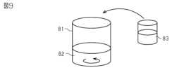
- 2-propanol is charged as a solvent 82 into the reaction vessel 81.
- a catalyst charging step S14 is performed.
- FIG. 9 in the catalyst charging step S14, first, stirring of the solvent 82 in the reaction vessel 81 is started. Then, ammonia water is put into the reaction vessel 81 as an aqueous solution 83 containing a catalyst.
- the catalyst in this embodiment is hydroxide ions, and functions as a catalyst that promotes hydrolysis of metal alkoxide 85, which will be described later.
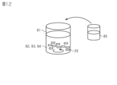
- the element loading step S15 is performed. As shown in FIG. 10, in the element loading step S15, a plurality of elements 20 formed in advance in the R-chamfering step S12 as described above are loaded into the reaction vessel 81 .
- the polymer charging step S16 is performed.
- polyvinylpyrrolidone is charged as the polymer 84 into the reaction vessel 81 .
- the polymer 84 put into the reaction vessel 81 is adsorbed on the outer surface 21 of the element body 20 .
- a metal alkoxide introduction step S17 is performed.
- liquid tetraethyl orthosilicate is charged into the reaction vessel 81 as the metal alkoxide 85 .
- Tetraethyl orthotetrasilicate is sometimes called tetraethoxysilane.
- the amount of the metal alkoxide 85 to be introduced in the metal alkoxide introduction step S17 is calculated based on the area of the outer surface 21 of the element 20 introduced in the element introduction step S15. Specifically, it is calculated by multiplying the amount of the metal alkoxide 85 per element body 20 necessary for forming the glass film 50 covering the outer surface 21 of the element body 20 by the number of element bodies 20 . .
- a film forming step S18 is performed.
- stirring of the solvent 82 started in the solvent charging step S13 is continued for a predetermined time after the metal alkoxide 85 is charged into the reaction vessel 81 in the metal alkoxide charging step S17.
- the glass film 50 containing the polymer 84 and moisture is formed by liquid phase reaction in the reaction vessel 81 .
- the water immersion step S19 is performed.
- the element body 20 is taken out from the reaction vessel 81 and immersed in water.
- part of the polymer 84 adsorbed on the outer surface 21 of the base body 20 is dissolved in water, and part of the glass component of the glass film 50 is partially removed.
- the drying step S20 is performed.
- the body 20 is taken out of water and dried.
- the sol-like glass film 50 is dried and becomes a gel-like glass film 50 .
- the conductor coating step S21 is performed.
- two portions of the surface of the glass film 50 one including the portion covering the first end surface 22A of the element body 20 and the other including the portion covering the second end surface 22B of the element body 20, are coated.
- Apply conductive paste to Specifically, the conductive paste is applied so as to cover the glass film 50 on the entire first end face 22A and part of the four side faces 22C. Also, the conductive paste is applied so as to cover the glass film 50 on the entire second end face 22B and part of the four side faces 22C.
- a curing step S22 is performed. Specifically, in the curing step S22, the glass film 50 and the element body 20 to which the conductor paste is applied are heated. As a result, the water and the polymer 84 are vaporized from the gel-like glass film 50, and as shown in FIG. 3, the glass film 50 covering the outer surface 21 of the element body 20 is baked and hardened. At this time, a through-hole 51 penetrating through the glass film 50 is formed due to the difference in the amount of heat shrinkage, bordering on the location where a part of the glass film 50 fell off in the water immersion step S19 described above.
- the first base electrode 61A and the second base electrode 62A are formed by baking the conductor paste applied in the conductor applying step S21.
- the base electrode forming process is composed of the conductor coating process S21 and the curing process S22. That is, in the present embodiment, the curing step S22 serves not only as a step of curing the glass film 50, but also as part of the base electrode forming step.
- the first base electrode 61A containing silver The palladium contained on the first internal electrode 41 side is attracted.
- the first penetrating portion 71 extends through the glass film 50 from the first internal electrode 41 toward the first base electrode 61A, thereby connecting the first internal electrode 41 and the first base electrode 61A.
- the plating step S23 is performed. Electroplating is performed on the portions of the first base electrode 61A and the second base electrode 62A. Specifically, in the plating step S23, electroplating of nickel is first performed. As a result, a nickel layer of the first metal layer 61B is formed on the surface of the first base electrode 61A. Also, a nickel layer of the second metal layer 62B is formed on the surface of the second base electrode 62A.
- the glass film 50 has the through holes 51 at the time of the plating step S23. Therefore, part of the element body 20 is exposed to the outside through the through hole 51 .
- the element body 20 exposed from the through-holes 51 is partially corroded by the plating solution used for nickel electroplating. As a result, recesses 26 are formed in portions of the base body 20 that are exposed from the through holes 51 .
- the tin layer of the first metal layer 61B is formed on the surface of the nickel layer of the first metal layer 61B.
- the nickel layer of the second metal layer 62B is formed on the surface of the nickel layer of the second metal layer 62B.
- the body 20 is a semiconductor, the interior of the recess 26 is also plated. Therefore, fillings 63 made of tin are formed in some recesses 26B of the plurality of recesses 26 .
- the electronic component 10 is formed.
- the thickness of the nickel layer in the first external electrode 61 and the second external electrode 62 is 2 ⁇ m.
- the opening area of the depression 26 of the electronic component 10 of Example 1 is 1.8 ⁇ m 2 .
- the area ratio of the depressions 26 of the electronic component 10 of Example 1 is 0.1%.
- the recess volume of the recess 26 of the electronic component 10 of Example 1 is 0.5 ⁇ m 3 .
- the thickness of the nickel layer in the first external electrode 61 and the second external electrode 62 is 4 ⁇ m.
- the opening area of the depression 26 of the electronic component 10 of Example 2 is 7.1 ⁇ 2 .
- the area ratio of the depressions 26 of the electronic component 10 of Example 2 is 0.5%.
- the recess volume of the recess 26 of the electronic component 10 of Example 2 is 4.1 ⁇ m 3 .
- the thickness of the nickel layer in the first external electrode 61 and the second external electrode 62 is 6 ⁇ m.
- the opening area of the depression 26 of the electronic component 10 of Example 3 is 28.5 ⁇ m 2 .
- the area ratio of the depressions 26 of the electronic component 10 of Example 3 is 1.8%.
- the recess volume of the recess 26 of the electronic component 10 of Example 3 is 31.8 ⁇ m 3 .
- the thickness of the nickel layer in the first external electrode 61 and the second external electrode 62 is 8 ⁇ m.
- the opening area of the depression 26 of the electronic component 10 of Example 4 is 114.7 ⁇ m 2 .
- the area ratio of the depressions 26 of the electronic component 10 of Example 4 is 6.8%.
- the recess volume of the recess 26 of the electronic component 10 of Example 4 is 246.9 ⁇ m 3 .
- the thickness of the nickel layer in the first external electrode 61 and the second external electrode 62 is 10 ⁇ m.
- the opening area of the depression 26 of the electronic component 10 of Example 5 is 429.0 ⁇ m 2 .
- the area ratio of the depressions 26 of the electronic component 10 of Example 5 is 45.4%.
- the recess volume of the recess 26 of the electronic component 10 of Example 5 is 1684.1 ⁇ m 3 .
- the thickness of the nickel layer in the first external electrode 61 and the second external electrode 62 is 12 ⁇ m.
- the opening area of the depression 26 of the electronic component 10 of Example 6 is 1963.5 ⁇ m 2 .
- the area ratio of the depressions 26 of the electronic component 10 of Example 6 is 58.6%.
- the recess volume of the recess 26 of the recess 26 of the electronic component 10 of Example 6 is 16493.4 ⁇ m 3 .
- the electronic component of the comparative example was manufactured by omitting the water immersion step S19 described above. Therefore, the electronic component of the comparative example does not have the through holes 51 and the recesses 26 at all. Moreover, in the electronic component of the comparative example, the thickness of the nickel layer in the first external electrode 61 and the second external electrode 62 is 2 ⁇ m.
- the thermal shock test was performed as follows. First, the number of samples of the electronic component to be evaluated was 30 pieces. Next, the electronic component to be evaluated was mounted on the substrate. Next, one cycle of thermal shock was defined as changing the temperature of the board on which the electronic component was mounted from ⁇ 55° C. to 125° C., and 100 cycles of this were performed. After that, when the number of cracks existing in the glass film 50 increased compared to before the thermal shock was applied, it was rated as NG (No Good), and when it did not change, it was rated as G (Good).
- the impact film peeling test was performed as follows. First, the number of samples of electronic components to be evaluated was 1,000. Next, the electronic parts to be evaluated were placed in one container, and the whole container was oscillated so as to rub against each other. After that, out of 1000 electronic components, when the number of electronic components whose glass film 50 was partially peeled off from the base body 20 was 10 or more, it was rated as NG, and when it was less than 10, it was rated as G.
- the migration test was conducted as follows. First, the number of samples of the electronic component to be evaluated was 18 pieces. Next, the electronic component to be evaluated was mounted on the substrate. Next, the temperature was 125° C. and the humidity was 95%, and the applied voltage was set to 3.2 V or less for 72 hours. After that, the presence or absence of a short circuit between the external electrodes due to migration was evaluated. Among the 18 electronic components, NG was given when the number of migration occurrences was 1 or more, and G was given when there were 0 of them.
- the evaluation result of the thermal shock test was G for the electronic components 10 of Examples 1 to 6. Further, in the electronic components 10 of Examples 1 to 6, the evaluation result of the impact film peeling test was G. On the other hand, in the electronic component of the comparative example, the evaluation result of the thermal shock test was NG. In addition, the evaluation test of the impact film peeling test was NG in the electronic component of the comparative example.
- the evaluation result of the migration test was G.
- the evaluation result of the migration test was NG.
- the plurality of depressions 26 are connected to the through holes 51 of the glass film 50 respectively. Therefore, as in the manufacturing method described above, the depressions 26 can be formed in the plating step S23 for forming the first external electrodes 61 and the second external electrodes 62, so there is no need to adopt a separate step for forming the depressions 26. .
- the filler 63 exists in the internal space of the recess 26B.
- the filler 63 is made of relatively soft metal and functions as a shock absorbing material. Therefore, even if force is applied from the outside of electronic component 10 toward depression 26B, the impact can be mitigated by filler 63 . Therefore, the force from the outside of the electronic component 10 can be alleviated from being directly transmitted to the element body 20 .
- the opening area of the depression 26 is 1 ⁇ m 2 or more and 2000 ⁇ m 2 or less. That is, the opening area of the depression 26 is not excessively large. Therefore, it is possible to prevent the strength of the element body 20 from being affected by the depression 26 being too large.
- the area ratio of the depressions 26 is 0.1% or more and 60.0% or less. If the area ratio is within this range, it is possible to prevent the plurality of depressions 26 from being connected to form a large depression, and the strength of the element body 20 to be adversely affected by the large depression.
- the recess volume which is the volume of the internal space of the recess 26, is 0.1 ⁇ m 3 or more and 20000 ⁇ m 3 or less. If the volume of the recess is within this range, it is unlikely that the recess 26 reaches the first internal electrode 41 or the second internal electrode 42 .
- the maximum depth H of the recess 26A with respect to the opening diameter D of the recess 26A is 25% or more. Since the depression 26A has a certain maximum depth H in this manner, the effect of dividing the force applied to the surface of the base body 20 can be reliably exhibited. Further, the maximum depth H of the recess 26A with respect to the opening diameter D of the recess 26A is 50% or less. Therefore, the recess 26A has a shape elongated in the direction along the outer surface 21 as a whole. Therefore, it is possible to prevent cracks or the like from occurring in the element body 20 starting from the recesses 26 .
- the electronic component 10 is not limited to the negative characteristic thermistor component.
- the electronic component 10 may be a thermistor component other than a negative characteristic component, a multilayer capacitor component, or an inductor component.
- the shape of the base body 20 is not limited to the example of the above embodiment.
- the base body 20 may have a polygonal columnar shape other than a quadrangular columnar shape having the central axis CA.
- the element body 20 may be the core of a wire-wound inductor component.
- the core may be in the shape of a so-called drum core.
- the core may have a columnar winding core and flanges provided at each end of the winding core.
- the material of the element body 20 is not limited to the example of the above embodiment.
- the material of the base body 20 may be a composite of resin and metal powder.
- the outer surface 21 of the element body 20 may not have the boundary surfaces 23 and the corner surfaces 24 .
- the boundary between the adjacent planes 22 on the outer surface 21 of the base body 20 is not chamfered, the boundary does not have a curved surface. Therefore, in such cases, the boundary surface 23 and the corner surface 24 may not exist.
- the shape of the first internal electrode 41 and the second internal electrode 42 does not matter as long as it can ensure electrical continuity with the corresponding first external electrode 61 and second external electrode 62 .
- the number of the first internal electrodes 41 and the number of the second internal electrodes 42 is not limited, and the number of internal electrodes may be one, or three or more.
- the thickness of the nickel layer of the first external electrode 61 may be less than 0.5 ⁇ m or greater than 10 ⁇ m.
- the depressions 26 are formed by nickel electroplating. By setting the thickness of the nickel layer of the first external electrode 61 to 0.5 ⁇ m or more and 10 ⁇ m or less, the size of the depression 26 can be formed within a preferable range from the viewpoint of the migration test. On the other hand, for example, even when the thickness of the nickel layer of the first external electrode 61 was larger than 10 ⁇ m, the evaluation results of the thermal shock test and the impact film peeling test were good.
- the thickness of the nickel layer of the first external electrode 61 is greater than 10 ⁇ m, it is possible to prevent the impact from being concentrated on a specific portion of the surface of the element body 20 .
- the configuration of the first external electrode 61 is not limited to the example of the above embodiment.
- the first external electrode 61 may be composed of only the first base electrode 61A, and the first metal layer 61B may not have a two-layer structure. If the first metal layer 61B has a nickel layer, the recesses 26 can be formed in the base body 20 by the manufacturing method exemplified in the embodiment. In this regard, the same applies to the second external electrode 62 as well.
- the combination of materials for the first internal electrode 41 and the first base electrode 61A is not limited to the combination of palladium and silver.
- it may be a combination of copper and nickel, copper and silver, silver and gold, nickel and cobalt, or nickel and gold.
- one may be silver and the other may be a combination of silver and palladium.
- one may be palladium and the other may be a combination of silver and palladium, or one may be copper and the other may be a combination of silver and palladium.
- one may be gold and the other may be a combination of silver and palladium.
- the Kirkendall effect may not be obtained depending on the combination of the first internal electrode 41 and the first base electrode 61A.
- the first end face 22A side of the base body 20 is polished to physically remove a portion of the glass film 50 so that the first internal electrodes 41 are exposed. do it.
- the first internal electrode 41 and the first base electrode 61A can be connected.
- the glass film 50 including the surface of the first base electrode 61A may be formed, and the glass film 50 covering the surface of the first base electrode 61A may be removed.
- the arrangement location of the first external electrode 61 is not limited to the example of the above embodiment.
- the first external electrode 61 may be arranged only on the first end surface 22A and one side surface 22C. In this regard, the same applies to the second external electrode 62 as well.
- the glass film 50 does not have to cover the first end surface 22A and the second end surface 22B.
- the range covered by the glass film 50 may be appropriately changed according to the shape of the element body 20, the positions of the first external electrode 61 and the second external electrode 62, and the like.
- the glass in the glass film 50 may be integrated with the glass in the first base electrode 61A by diffusing.
- the maximum depth H of the recess 26 with respect to the length of the opening diameter D of the recess 26 may be less than 25% or may be greater than 50%.
- the relationship between the opening diameter D and the maximum depth H may be changed as appropriate depending on the shape of the recess 26 .
- a plurality of depressions 26 may be connected, or the depressions 26 may be recessed considerably deeply.
- the dimple volume may be greater than 20000 ⁇ m 3 .
- the strength of the base body 20 can be ensured even if the volume of the recess is correspondingly large.
- the area ratio of the depressions 26 may be greater than 60.0%.
- the size of the base body 20 is appropriately large, the strength of the base body 20 can be ensured even if the area ratio of the depressions 26 is correspondingly large.
- the opening area may be greater than 2000 ⁇ m 2 .
- the strength of the base body 20 can be ensured even if the opening area is correspondingly large.
- the plurality of recesses 26 may have only one of the recesses 26A in which nothing exists in the internal space and the recesses 26B in which the filler 63 exists in the internal space.
- the plurality of recesses 26 may not have recesses 26B with fillers 63 in the interior space.
- the filling 63 does not have to cover the entire inner surface of the recess 26B. That is, the filler 63 may cover only part of the inner surface of the recess 26B. In this case, the filler 63 does not protrude from the recess 26B. That is, when electronic component 10 is viewed in a direction orthogonal to outer surface 21, filler 63 may cover a range narrower than depression 26B.
- the filler 63 should be positioned at least in the internal space of the recess 26B.
- the through-hole 51 may be larger than the outer edge of the recess 26 or smaller than the outer edge of the recess 26 when the electronic component 10 is viewed in a direction perpendicular to the outer surface 21 . may be If the size of the through-hole 51 is smaller than the outer edge of the recess 26, the glass film 50 will appear to be floating from the inner surface of the recess 26. FIG. Even in this case, since the glass film 50 is not in contact with the inner surface of the recess 26 , the inner surface of the recess 26 is not covered with the glass film 50 .
- the method of manufacturing the electronic component 10 is not limited to the example of the above embodiment.
- the depressions 26 may be formed by mechanical cutting, or the glass film 50 may be formed by attaching a sheet-like thin film to the element body 20 .
- the glass film 50 does not have to have the through holes 51 .
Landscapes
- Engineering & Computer Science (AREA)
- Microelectronics & Electronic Packaging (AREA)
- Power Engineering (AREA)
- Physics & Mathematics (AREA)
- Electromagnetism (AREA)
- Manufacturing & Machinery (AREA)
- Fixed Capacitors And Capacitor Manufacturing Machines (AREA)
- Coils Or Transformers For Communication (AREA)
Priority Applications (2)
| Application Number | Priority Date | Filing Date | Title |
|---|---|---|---|
| JP2023559431A JP7658455B2 (ja) | 2021-11-09 | 2022-08-10 | 電子部品 |
| US18/536,992 US20240112835A1 (en) | 2021-11-09 | 2023-12-12 | Electronic component |
Applications Claiming Priority (2)
| Application Number | Priority Date | Filing Date | Title |
|---|---|---|---|
| JP2021182603 | 2021-11-09 | ||
| JP2021-182603 | 2021-11-09 |
Related Child Applications (1)
| Application Number | Title | Priority Date | Filing Date |
|---|---|---|---|
| US18/536,992 Continuation US20240112835A1 (en) | 2021-11-09 | 2023-12-12 | Electronic component |
Publications (1)
| Publication Number | Publication Date |
|---|---|
| WO2023084858A1 true WO2023084858A1 (ja) | 2023-05-19 |
Family
ID=86335586
Family Applications (1)
| Application Number | Title | Priority Date | Filing Date |
|---|---|---|---|
| PCT/JP2022/030676 Ceased WO2023084858A1 (ja) | 2021-11-09 | 2022-08-10 | 電子部品 |
Country Status (3)
| Country | Link |
|---|---|
| US (1) | US20240112835A1 (https=) |
| JP (1) | JP7658455B2 (https=) |
| WO (1) | WO2023084858A1 (https=) |
Cited By (1)
| Publication number | Priority date | Publication date | Assignee | Title |
|---|---|---|---|---|
| WO2025115910A1 (ja) * | 2023-11-29 | 2025-06-05 | 株式会社村田製作所 | 電子部品及び電子部品の製造方法 |
Citations (5)
| Publication number | Priority date | Publication date | Assignee | Title |
|---|---|---|---|---|
| JP2004311676A (ja) * | 2003-04-07 | 2004-11-04 | Murata Mfg Co Ltd | チップ状積層セラミック電子部品の製造方法およびチップ状積層セラミック電子部品 |
| JP2010080703A (ja) * | 2008-09-26 | 2010-04-08 | Tdk Corp | セラミック積層電子部品およびその製造方法 |
| JP2011176238A (ja) * | 2010-02-25 | 2011-09-08 | Tdk Corp | チップ型電子部品 |
| CN109478465A (zh) * | 2016-07-01 | 2019-03-15 | 摩达伊诺琴股份有限公司 | 芯片构件及其制造方法 |
| US20190141825A1 (en) * | 2016-05-30 | 2019-05-09 | Moda-Innochips Co., Ltd. | Contactor |
Family Cites Families (1)
| Publication number | Priority date | Publication date | Assignee | Title |
|---|---|---|---|---|
| JP5304757B2 (ja) | 2010-09-06 | 2013-10-02 | Tdk株式会社 | セラミック積層ptcサーミスタ |
-
2022
- 2022-08-10 JP JP2023559431A patent/JP7658455B2/ja active Active
- 2022-08-10 WO PCT/JP2022/030676 patent/WO2023084858A1/ja not_active Ceased
-
2023
- 2023-12-12 US US18/536,992 patent/US20240112835A1/en active Pending
Patent Citations (5)
| Publication number | Priority date | Publication date | Assignee | Title |
|---|---|---|---|---|
| JP2004311676A (ja) * | 2003-04-07 | 2004-11-04 | Murata Mfg Co Ltd | チップ状積層セラミック電子部品の製造方法およびチップ状積層セラミック電子部品 |
| JP2010080703A (ja) * | 2008-09-26 | 2010-04-08 | Tdk Corp | セラミック積層電子部品およびその製造方法 |
| JP2011176238A (ja) * | 2010-02-25 | 2011-09-08 | Tdk Corp | チップ型電子部品 |
| US20190141825A1 (en) * | 2016-05-30 | 2019-05-09 | Moda-Innochips Co., Ltd. | Contactor |
| CN109478465A (zh) * | 2016-07-01 | 2019-03-15 | 摩达伊诺琴股份有限公司 | 芯片构件及其制造方法 |
Cited By (1)
| Publication number | Priority date | Publication date | Assignee | Title |
|---|---|---|---|---|
| WO2025115910A1 (ja) * | 2023-11-29 | 2025-06-05 | 株式会社村田製作所 | 電子部品及び電子部品の製造方法 |
Also Published As
| Publication number | Publication date |
|---|---|
| JPWO2023084858A1 (https=) | 2023-05-19 |
| US20240112835A1 (en) | 2024-04-04 |
| JP7658455B2 (ja) | 2025-04-08 |
Similar Documents
| Publication | Publication Date | Title |
|---|---|---|
| US11302480B2 (en) | Ceramic electronic device with varying roughness terminal electrode | |
| CN109727770B (zh) | 层叠陶瓷电容器 | |
| US8743528B2 (en) | Capacitor | |
| TW201801105A (zh) | 積層線圈零件 | |
| CN112242253B (zh) | 电子部件 | |
| US11469050B2 (en) | Multilayer ceramic electronic component and manufacturing method thereof | |
| US20250232899A1 (en) | Electronic component and film forming method | |
| JP2022014536A (ja) | 電子部品 | |
| WO2023084858A1 (ja) | 電子部品 | |
| JP2022014532A (ja) | 電子部品及び電子部品の製造方法 | |
| JP2022014534A (ja) | 電子部品 | |
| JP2022014535A (ja) | 電子部品 | |
| WO2024029252A1 (ja) | 電子部品 | |
| US12488917B2 (en) | Electronic component | |
| WO2023084878A1 (ja) | 電子部品 | |
| KR101959766B1 (ko) | 세라믹 콘덴서 | |
| JP2011124403A (ja) | 電子部品の製造方法 | |
| CN120359585A (zh) | 层叠陶瓷电子部件 | |
| WO2024029251A1 (ja) | 電子部品 | |
| JP3981125B2 (ja) | 積層型チップバリスタ及びその製造方法 | |
| CN120727460A (zh) | 层叠陶瓷电子部件 | |
| WO2025094421A1 (ja) | 積層セラミック電子部品及び積層セラミック電子部品の製造方法 | |
| WO2025105153A1 (ja) | 電子部品、および電子部品の製造方法 | |
| KR20250131219A (ko) | 적층 세라믹 콘덴서 | |
| CN118156034A (zh) | 多层电子组件 |
Legal Events
| Date | Code | Title | Description |
|---|---|---|---|
| 121 | Ep: the epo has been informed by wipo that ep was designated in this application |
Ref document number: 22892361 Country of ref document: EP Kind code of ref document: A1 |
|
| ENP | Entry into the national phase |
Ref document number: 2023559431 Country of ref document: JP Kind code of ref document: A |
|
| 122 | Ep: pct application non-entry in european phase |
Ref document number: 22892361 Country of ref document: EP Kind code of ref document: A1 |