WO2023074531A1 - Metal laminate, method for manufacturing same, and printed wiring board - Google Patents
Metal laminate, method for manufacturing same, and printed wiring board Download PDFInfo
- Publication number
- WO2023074531A1 WO2023074531A1 PCT/JP2022/039148 JP2022039148W WO2023074531A1 WO 2023074531 A1 WO2023074531 A1 WO 2023074531A1 JP 2022039148 W JP2022039148 W JP 2022039148W WO 2023074531 A1 WO2023074531 A1 WO 2023074531A1
- Authority
- WO
- WIPO (PCT)
- Prior art keywords
- metal
- layer
- dielectric film
- low dielectric
- foil
- Prior art date
Links
- 229910052751 metal Inorganic materials 0.000 title claims abstract description 492
- 239000002184 metal Substances 0.000 title claims abstract description 490
- 238000000034 method Methods 0.000 title claims abstract description 51
- 238000004519 manufacturing process Methods 0.000 title claims abstract description 29
- 239000011888 foil Substances 0.000 claims abstract description 173
- RYGMFSIKBFXOCR-UHFFFAOYSA-N Copper Chemical compound [Cu] RYGMFSIKBFXOCR-UHFFFAOYSA-N 0.000 claims description 155
- 239000002648 laminated material Substances 0.000 claims description 135
- 239000011889 copper foil Substances 0.000 claims description 104
- 238000000992 sputter etching Methods 0.000 claims description 57
- 239000010949 copper Substances 0.000 claims description 51
- 229910052802 copper Inorganic materials 0.000 claims description 48
- PXHVJJICTQNCMI-UHFFFAOYSA-N Nickel Chemical compound [Ni] PXHVJJICTQNCMI-UHFFFAOYSA-N 0.000 claims description 34
- 238000005096 rolling process Methods 0.000 claims description 27
- 230000003213 activating effect Effects 0.000 claims description 21
- 229910045601 alloy Inorganic materials 0.000 claims description 19
- 239000000956 alloy Substances 0.000 claims description 19
- 238000010438 heat treatment Methods 0.000 claims description 18
- 229910052759 nickel Inorganic materials 0.000 claims description 18
- 230000009467 reduction Effects 0.000 claims description 16
- 239000011651 chromium Substances 0.000 claims description 14
- 239000007769 metal material Substances 0.000 claims description 14
- 229910052804 chromium Inorganic materials 0.000 claims description 13
- VYZAMTAEIAYCRO-UHFFFAOYSA-N Chromium Chemical compound [Cr] VYZAMTAEIAYCRO-UHFFFAOYSA-N 0.000 claims description 11
- QVGXLLKOCUKJST-UHFFFAOYSA-N atomic oxygen Chemical compound [O] QVGXLLKOCUKJST-UHFFFAOYSA-N 0.000 claims description 9
- 239000001301 oxygen Substances 0.000 claims description 7
- 229910052760 oxygen Inorganic materials 0.000 claims description 7
- 238000002844 melting Methods 0.000 claims description 5
- 230000008018 melting Effects 0.000 claims description 5
- 238000003475 lamination Methods 0.000 abstract description 4
- 239000010410 layer Substances 0.000 description 319
- 229920000106 Liquid crystal polymer Polymers 0.000 description 65
- 239000004977 Liquid-crystal polymers (LCPs) Substances 0.000 description 65
- 239000007789 gas Substances 0.000 description 46
- 239000002245 particle Substances 0.000 description 25
- 230000000052 comparative effect Effects 0.000 description 22
- 238000001994 activation Methods 0.000 description 16
- 230000004913 activation Effects 0.000 description 14
- -1 polyfluoroethylene Polymers 0.000 description 12
- 230000005540 biological transmission Effects 0.000 description 11
- 239000000463 material Substances 0.000 description 11
- 239000011261 inert gas Substances 0.000 description 9
- 238000009823 thermal lamination Methods 0.000 description 9
- 230000008569 process Effects 0.000 description 8
- 238000004544 sputter deposition Methods 0.000 description 8
- XEEYBQQBJWHFJM-UHFFFAOYSA-N Iron Chemical compound [Fe] XEEYBQQBJWHFJM-UHFFFAOYSA-N 0.000 description 7
- 229910052725 zinc Inorganic materials 0.000 description 7
- 239000011701 zinc Substances 0.000 description 7
- XKRFYHLGVUSROY-UHFFFAOYSA-N Argon Chemical compound [Ar] XKRFYHLGVUSROY-UHFFFAOYSA-N 0.000 description 6
- 230000000694 effects Effects 0.000 description 6
- 238000007747 plating Methods 0.000 description 6
- BASFCYQUMIYNBI-UHFFFAOYSA-N platinum Chemical compound [Pt] BASFCYQUMIYNBI-UHFFFAOYSA-N 0.000 description 6
- 239000006087 Silane Coupling Agent Substances 0.000 description 5
- 238000001816 cooling Methods 0.000 description 5
- 238000005304 joining Methods 0.000 description 5
- 239000000758 substrate Substances 0.000 description 5
- IJGRMHOSHXDMSA-UHFFFAOYSA-N Atomic nitrogen Chemical compound N#N IJGRMHOSHXDMSA-UHFFFAOYSA-N 0.000 description 4
- 229910000881 Cu alloy Inorganic materials 0.000 description 4
- 229910000990 Ni alloy Inorganic materials 0.000 description 4
- HCHKCACWOHOZIP-UHFFFAOYSA-N Zinc Chemical compound [Zn] HCHKCACWOHOZIP-UHFFFAOYSA-N 0.000 description 4
- 229910052786 argon Inorganic materials 0.000 description 4
- VNNRSPGTAMTISX-UHFFFAOYSA-N chromium nickel Chemical compound [Cr].[Ni] VNNRSPGTAMTISX-UHFFFAOYSA-N 0.000 description 4
- 238000010586 diagram Methods 0.000 description 4
- 229910052742 iron Inorganic materials 0.000 description 4
- 238000005259 measurement Methods 0.000 description 4
- 238000005065 mining Methods 0.000 description 4
- 229910001120 nichrome Inorganic materials 0.000 description 4
- 238000000879 optical micrograph Methods 0.000 description 4
- 238000007788 roughening Methods 0.000 description 4
- 229910052719 titanium Inorganic materials 0.000 description 4
- 239000010936 titanium Substances 0.000 description 4
- 239000004642 Polyimide Substances 0.000 description 3
- BQCADISMDOOEFD-UHFFFAOYSA-N Silver Chemical compound [Ag] BQCADISMDOOEFD-UHFFFAOYSA-N 0.000 description 3
- ATJFFYVFTNAWJD-UHFFFAOYSA-N Tin Chemical compound [Sn] ATJFFYVFTNAWJD-UHFFFAOYSA-N 0.000 description 3
- RTAQQCXQSZGOHL-UHFFFAOYSA-N Titanium Chemical compound [Ti] RTAQQCXQSZGOHL-UHFFFAOYSA-N 0.000 description 3
- 239000000654 additive Substances 0.000 description 3
- 229910017052 cobalt Inorganic materials 0.000 description 3
- 239000010941 cobalt Substances 0.000 description 3
- GUTLYIVDDKVIGB-UHFFFAOYSA-N cobalt atom Chemical compound [Co] GUTLYIVDDKVIGB-UHFFFAOYSA-N 0.000 description 3
- 238000005530 etching Methods 0.000 description 3
- PCHJSUWPFVWCPO-UHFFFAOYSA-N gold Chemical compound [Au] PCHJSUWPFVWCPO-UHFFFAOYSA-N 0.000 description 3
- 229910052737 gold Inorganic materials 0.000 description 3
- 239000010931 gold Substances 0.000 description 3
- 230000006872 improvement Effects 0.000 description 3
- 238000010030 laminating Methods 0.000 description 3
- 239000002923 metal particle Substances 0.000 description 3
- 229910052697 platinum Inorganic materials 0.000 description 3
- 229920001721 polyimide Polymers 0.000 description 3
- 238000012545 processing Methods 0.000 description 3
- 229910052709 silver Inorganic materials 0.000 description 3
- 239000004332 silver Substances 0.000 description 3
- 239000002356 single layer Substances 0.000 description 3
- 238000001179 sorption measurement Methods 0.000 description 3
- 239000000126 substance Substances 0.000 description 3
- 230000003746 surface roughness Effects 0.000 description 3
- 239000011135 tin Substances 0.000 description 3
- 229910052718 tin Inorganic materials 0.000 description 3
- YXIWHUQXZSMYRE-UHFFFAOYSA-N 1,3-benzothiazole-2-thiol Chemical compound C1=CC=C2SC(S)=NC2=C1 YXIWHUQXZSMYRE-UHFFFAOYSA-N 0.000 description 2
- FJKROLUGYXJWQN-UHFFFAOYSA-N 4-hydroxybenzoic acid Chemical compound OC(=O)C1=CC=C(O)C=C1 FJKROLUGYXJWQN-UHFFFAOYSA-N 0.000 description 2
- 101001134276 Homo sapiens S-methyl-5'-thioadenosine phosphorylase Proteins 0.000 description 2
- KDLHZDBZIXYQEI-UHFFFAOYSA-N Palladium Chemical compound [Pd] KDLHZDBZIXYQEI-UHFFFAOYSA-N 0.000 description 2
- 239000004952 Polyamide Substances 0.000 description 2
- 102100022050 Protein canopy homolog 2 Human genes 0.000 description 2
- NINIDFKCEFEMDL-UHFFFAOYSA-N Sulfur Chemical compound [S] NINIDFKCEFEMDL-UHFFFAOYSA-N 0.000 description 2
- WGLPBDUCMAPZCE-UHFFFAOYSA-N Trioxochromium Chemical compound O=[Cr](=O)=O WGLPBDUCMAPZCE-UHFFFAOYSA-N 0.000 description 2
- XLOMVQKBTHCTTD-UHFFFAOYSA-N Zinc monoxide Chemical compound [Zn]=O XLOMVQKBTHCTTD-UHFFFAOYSA-N 0.000 description 2
- 229910052782 aluminium Inorganic materials 0.000 description 2
- XAGFODPZIPBFFR-UHFFFAOYSA-N aluminium Chemical compound [Al] XAGFODPZIPBFFR-UHFFFAOYSA-N 0.000 description 2
- 230000015572 biosynthetic process Effects 0.000 description 2
- 150000001735 carboxylic acids Chemical class 0.000 description 2
- ZCDOYSPFYFSLEW-UHFFFAOYSA-N chromate(2-) Chemical compound [O-][Cr]([O-])(=O)=O ZCDOYSPFYFSLEW-UHFFFAOYSA-N 0.000 description 2
- 229910000423 chromium oxide Inorganic materials 0.000 description 2
- 230000006378 damage Effects 0.000 description 2
- 229910052743 krypton Inorganic materials 0.000 description 2
- DNNSSWSSYDEUBZ-UHFFFAOYSA-N krypton atom Chemical compound [Kr] DNNSSWSSYDEUBZ-UHFFFAOYSA-N 0.000 description 2
- 229910052750 molybdenum Inorganic materials 0.000 description 2
- 229910052754 neon Inorganic materials 0.000 description 2
- GKAOGPIIYCISHV-UHFFFAOYSA-N neon atom Chemical compound [Ne] GKAOGPIIYCISHV-UHFFFAOYSA-N 0.000 description 2
- 229910052757 nitrogen Inorganic materials 0.000 description 2
- 150000002894 organic compounds Chemical class 0.000 description 2
- 230000003647 oxidation Effects 0.000 description 2
- 238000007254 oxidation reaction Methods 0.000 description 2
- 229920002647 polyamide Polymers 0.000 description 2
- 239000002861 polymer material Substances 0.000 description 2
- 239000011164 primary particle Substances 0.000 description 2
- 229920005989 resin Polymers 0.000 description 2
- 239000011347 resin Substances 0.000 description 2
- 150000004756 silanes Chemical class 0.000 description 2
- 238000002791 soaking Methods 0.000 description 2
- 229910052717 sulfur Inorganic materials 0.000 description 2
- 239000011593 sulfur Substances 0.000 description 2
- 238000012360 testing method Methods 0.000 description 2
- 238000003466 welding Methods 0.000 description 2
- 230000037303 wrinkles Effects 0.000 description 2
- 229910052724 xenon Inorganic materials 0.000 description 2
- FHNFHKCVQCLJFQ-UHFFFAOYSA-N xenon atom Chemical compound [Xe] FHNFHKCVQCLJFQ-UHFFFAOYSA-N 0.000 description 2
- AZUHEGMJQWJCFQ-UHFFFAOYSA-N 1,1-bis(2h-benzotriazol-4-ylmethyl)urea Chemical compound C1=CC2=NNN=C2C(CN(CC=2C3=NNN=C3C=CC=2)C(=O)N)=C1 AZUHEGMJQWJCFQ-UHFFFAOYSA-N 0.000 description 1
- WZRRRFSJFQTGGB-UHFFFAOYSA-N 1,3,5-triazinane-2,4,6-trithione Chemical compound S=C1NC(=S)NC(=S)N1 WZRRRFSJFQTGGB-UHFFFAOYSA-N 0.000 description 1
- YHMYGUUIMTVXNW-UHFFFAOYSA-N 1,3-dihydrobenzimidazole-2-thione Chemical compound C1=CC=C2NC(S)=NC2=C1 YHMYGUUIMTVXNW-UHFFFAOYSA-N 0.000 description 1
- KFJDQPJLANOOOB-UHFFFAOYSA-N 2h-benzotriazole-4-carboxylic acid Chemical compound OC(=O)C1=CC=CC2=NNN=C12 KFJDQPJLANOOOB-UHFFFAOYSA-N 0.000 description 1
- 229940090248 4-hydroxybenzoic acid Drugs 0.000 description 1
- NSPMIYGKQJPBQR-UHFFFAOYSA-N 4H-1,2,4-triazole Chemical compound C=1N=CNN=1 NSPMIYGKQJPBQR-UHFFFAOYSA-N 0.000 description 1
- KLSJWNVTNUYHDU-UHFFFAOYSA-N Amitrole Chemical compound NC1=NC=NN1 KLSJWNVTNUYHDU-UHFFFAOYSA-N 0.000 description 1
- 229910001369 Brass Inorganic materials 0.000 description 1
- 229910000599 Cr alloy Inorganic materials 0.000 description 1
- 229920000089 Cyclic olefin copolymer Polymers 0.000 description 1
- MYMOFIZGZYHOMD-UHFFFAOYSA-N Dioxygen Chemical compound O=O MYMOFIZGZYHOMD-UHFFFAOYSA-N 0.000 description 1
- 239000004593 Epoxy Substances 0.000 description 1
- 240000007594 Oryza sativa Species 0.000 description 1
- 235000007164 Oryza sativa Nutrition 0.000 description 1
- 239000004962 Polyamide-imide Substances 0.000 description 1
- 239000004697 Polyetherimide Substances 0.000 description 1
- QCWXUUIWCKQGHC-UHFFFAOYSA-N Zirconium Chemical compound [Zr] QCWXUUIWCKQGHC-UHFFFAOYSA-N 0.000 description 1
- VDGMIGHRDCJLMN-UHFFFAOYSA-N [Cu].[Co].[Ni] Chemical compound [Cu].[Co].[Ni] VDGMIGHRDCJLMN-UHFFFAOYSA-N 0.000 description 1
- 125000003118 aryl group Chemical group 0.000 description 1
- QRUDEWIWKLJBPS-UHFFFAOYSA-N benzotriazole Chemical compound C1=CC=C2N[N][N]C2=C1 QRUDEWIWKLJBPS-UHFFFAOYSA-N 0.000 description 1
- 239000010951 brass Substances 0.000 description 1
- 230000015556 catabolic process Effects 0.000 description 1
- 239000011248 coating agent Substances 0.000 description 1
- 238000000576 coating method Methods 0.000 description 1
- NVIVJPRCKQTWLY-UHFFFAOYSA-N cobalt nickel Chemical compound [Co][Ni][Co] NVIVJPRCKQTWLY-UHFFFAOYSA-N 0.000 description 1
- 238000006731 degradation reaction Methods 0.000 description 1
- 230000006866 deterioration Effects 0.000 description 1
- 230000002542 deteriorative effect Effects 0.000 description 1
- 150000001991 dicarboxylic acids Chemical class 0.000 description 1
- 229910001882 dioxygen Inorganic materials 0.000 description 1
- 238000007772 electroless plating Methods 0.000 description 1
- 238000009713 electroplating Methods 0.000 description 1
- 238000005516 engineering process Methods 0.000 description 1
- 239000003822 epoxy resin Substances 0.000 description 1
- 238000011156 evaluation Methods 0.000 description 1
- 150000002460 imidazoles Chemical class 0.000 description 1
- 238000007654 immersion Methods 0.000 description 1
- 238000009413 insulation Methods 0.000 description 1
- 239000011229 interlayer Substances 0.000 description 1
- JEIPFZHSYJVQDO-UHFFFAOYSA-N iron(III) oxide Inorganic materials O=[Fe]O[Fe]=O JEIPFZHSYJVQDO-UHFFFAOYSA-N 0.000 description 1
- 239000012948 isocyanate Substances 0.000 description 1
- 239000004973 liquid crystal related substance Substances 0.000 description 1
- 150000002739 metals Chemical class 0.000 description 1
- 238000010295 mobile communication Methods 0.000 description 1
- 150000002763 monocarboxylic acids Chemical class 0.000 description 1
- 230000001590 oxidative effect Effects 0.000 description 1
- 229910052763 palladium Inorganic materials 0.000 description 1
- 229910052698 phosphorus Inorganic materials 0.000 description 1
- 229920002312 polyamide-imide Polymers 0.000 description 1
- 229920000647 polyepoxide Polymers 0.000 description 1
- 229920001225 polyester resin Polymers 0.000 description 1
- 239000004645 polyester resin Substances 0.000 description 1
- 229920001601 polyetherimide Polymers 0.000 description 1
- 229920000139 polyethylene terephthalate Polymers 0.000 description 1
- 239000005020 polyethylene terephthalate Substances 0.000 description 1
- 229920000642 polymer Polymers 0.000 description 1
- 229920001343 polytetrafluoroethylene Polymers 0.000 description 1
- 239000004810 polytetrafluoroethylene Substances 0.000 description 1
- 238000002360 preparation method Methods 0.000 description 1
- 230000002265 prevention Effects 0.000 description 1
- 239000011241 protective layer Substances 0.000 description 1
- 235000009566 rice Nutrition 0.000 description 1
- 239000011163 secondary particle Substances 0.000 description 1
- FZHAPNGMFPVSLP-UHFFFAOYSA-N silanamine Chemical class [SiH3]N FZHAPNGMFPVSLP-UHFFFAOYSA-N 0.000 description 1
- 238000005507 spraying Methods 0.000 description 1
- 239000010935 stainless steel Substances 0.000 description 1
- 229910001220 stainless steel Inorganic materials 0.000 description 1
- TXDNPSYEJHXKMK-UHFFFAOYSA-N sulfanylsilane Chemical class S[SiH3] TXDNPSYEJHXKMK-UHFFFAOYSA-N 0.000 description 1
- 239000002344 surface layer Substances 0.000 description 1
- 229910052721 tungsten Inorganic materials 0.000 description 1
- 238000007740 vapor deposition Methods 0.000 description 1
- 239000011787 zinc oxide Substances 0.000 description 1
- 229910052726 zirconium Inorganic materials 0.000 description 1
Images


Classifications
-
- B—PERFORMING OPERATIONS; TRANSPORTING
- B32—LAYERED PRODUCTS
- B32B—LAYERED PRODUCTS, i.e. PRODUCTS BUILT-UP OF STRATA OF FLAT OR NON-FLAT, e.g. CELLULAR OR HONEYCOMB, FORM
- B32B15/00—Layered products comprising a layer of metal
- B32B15/01—Layered products comprising a layer of metal all layers being exclusively metallic
-
- B—PERFORMING OPERATIONS; TRANSPORTING
- B32—LAYERED PRODUCTS
- B32B—LAYERED PRODUCTS, i.e. PRODUCTS BUILT-UP OF STRATA OF FLAT OR NON-FLAT, e.g. CELLULAR OR HONEYCOMB, FORM
- B32B15/00—Layered products comprising a layer of metal
- B32B15/04—Layered products comprising a layer of metal comprising metal as the main or only constituent of a layer, which is next to another layer of the same or of a different material
- B32B15/08—Layered products comprising a layer of metal comprising metal as the main or only constituent of a layer, which is next to another layer of the same or of a different material of synthetic resin
-
- C—CHEMISTRY; METALLURGY
- C23—COATING METALLIC MATERIAL; COATING MATERIAL WITH METALLIC MATERIAL; CHEMICAL SURFACE TREATMENT; DIFFUSION TREATMENT OF METALLIC MATERIAL; COATING BY VACUUM EVAPORATION, BY SPUTTERING, BY ION IMPLANTATION OR BY CHEMICAL VAPOUR DEPOSITION, IN GENERAL; INHIBITING CORROSION OF METALLIC MATERIAL OR INCRUSTATION IN GENERAL
- C23C—COATING METALLIC MATERIAL; COATING MATERIAL WITH METALLIC MATERIAL; SURFACE TREATMENT OF METALLIC MATERIAL BY DIFFUSION INTO THE SURFACE, BY CHEMICAL CONVERSION OR SUBSTITUTION; COATING BY VACUUM EVAPORATION, BY SPUTTERING, BY ION IMPLANTATION OR BY CHEMICAL VAPOUR DEPOSITION, IN GENERAL
- C23C26/00—Coating not provided for in groups C23C2/00 - C23C24/00
-
- H—ELECTRICITY
- H05—ELECTRIC TECHNIQUES NOT OTHERWISE PROVIDED FOR
- H05K—PRINTED CIRCUITS; CASINGS OR CONSTRUCTIONAL DETAILS OF ELECTRIC APPARATUS; MANUFACTURE OF ASSEMBLAGES OF ELECTRICAL COMPONENTS
- H05K3/00—Apparatus or processes for manufacturing printed circuits
-
- H—ELECTRICITY
- H05—ELECTRIC TECHNIQUES NOT OTHERWISE PROVIDED FOR
- H05K—PRINTED CIRCUITS; CASINGS OR CONSTRUCTIONAL DETAILS OF ELECTRIC APPARATUS; MANUFACTURE OF ASSEMBLAGES OF ELECTRICAL COMPONENTS
- H05K3/00—Apparatus or processes for manufacturing printed circuits
- H05K3/38—Improvement of the adhesion between the insulating substrate and the metal
Definitions
- the present invention relates to a metal laminated material, a method for manufacturing the same, and a printed wiring board.
- a metal laminate material in which a metal foil such as a copper foil is laminated on a low-dielectric film is known.
- 5th generation mobile communication system (5G) services have started in various countries, and there is a demand for laminated metal materials that are excellent in the frequency band of 5G, that is, in high-frequency characteristics.
- a metal foil having a roughened bonding surface is thermally and compression-bonded by a thermal lamination method.
- a thermal lamination method a metal foil with a roughened surface is used, and the low-dielectric film is softened by raising the temperature to near the melting point, and the roughened particles on the metal foil surface are removed from the inside of the low-dielectric film. It is deeply buried in the surface, and the adhesion is secured by the so-called anchor effect.
- Patent Document 1 discloses a surface-treated copper foil having a roughened surface, a copper-clad laminate obtained by laminating the copper foil on an insulating substrate, and a printed wiring board using the copper-clad laminate. and discloses that the copper-clad laminate can be produced by a thermal lamination method.
- an object of the present invention is to provide a metal laminated material that achieves both high-frequency characteristics and adhesion at the interface between layers.
- the present inventors have found that by producing a metal laminated material by the surface activation bonding method, the metal foil can be a low dielectric film while maintaining the smoothness of the surface.
- the present inventors have found that it is possible to laminate a layer on the same layer, and that both high-frequency characteristics and adhesion at the interface of the layer can be achieved, and the invention has been completed. That is, the gist of the present invention is as follows.
- FIG. 4 is a schematic cross-sectional view showing another aspect of the metal laminate material of the first embodiment of the present invention
- FIG. 4 is a schematic cross-sectional view showing a laminated metal material according to one aspect of the second embodiment of the present invention
- FIG. 11 is a schematic cross-sectional view showing another aspect of the metal laminate material of the second embodiment of the present invention
- FIG. 5A shows an enlarged schematic diagram of a cross section of the metal laminate 1A.
- FIG. 5B shows an enlarged schematic diagram of the cross section of the convex portion of the metal foil.
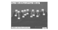
- FIG. 1 shows a cross-sectional photograph of the metal laminate material of Example 1.
- FIG. 4 shows a cross-sectional photograph of the metal laminate material of Example 2.
- FIG. 4 shows a cross-sectional photograph of the metal laminate material of Example 3.
- FIG. 4 shows a cross-sectional photograph of the metal laminate material of Example 4.
- FIG. 4 shows a cross-sectional photograph of the metal laminate material of Example 6.
- FIG. 4 shows a cross-sectional photograph of the metal laminate material of Example 7.
- FIG. 4 shows a cross-sectional photograph of the metal laminate material of Example 8.
- FIG. 4 shows a cross-sectional photograph of the metal laminate material of Example 14.
- FIG. 1 shows a cross-sectional photograph of a metal laminate material of Comparative Example 1.
- FIG. 4 shows a cross-sectional photograph of the metal laminate material of Comparative Example 2.
- the present invention relates to a laminated metal material in which at least one metal layer including a metal foil is laminated on at least one surface of a low dielectric film.
- the metal laminate of the present invention includes a low dielectric film laminated with a metal layer on one side and a low dielectric film laminated with a metal layer on both sides.
- the metal laminate material of the present invention since the surface of the metal foil on the low dielectric film side is smooth, the metal laminate material has excellent high-frequency characteristics, and the low dielectric film and the metal layer have sufficient adhesion. is.
- metal laminated material of the first embodiment of the present invention will be described below.
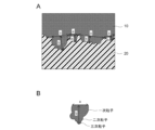
- FIG. 1 is a schematic cross-sectional view showing a laminated metal material according to one aspect of the first embodiment of the present invention. As shown in FIG. 1, in the metal laminated material 1A of the first embodiment, a metal layer 10 made of metal foil is laminated on one surface of a low dielectric film 20 .
- FIG. 2 is a schematic cross-sectional view showing another aspect of the metal laminate material of the first embodiment of the present invention.
- a metal foil with a carrier having an ultra-thin metal layer, a release layer, and a carrier layer is used as the metal foil.
- a metal layer 10 made of a metal foil with a carrier is laminated on one surface of a low dielectric film 20 .
- the metal layer 10 is laminated in order of the ultra-thin metal layer 14, the release layer 13, and the carrier layer 12 from the low dielectric film 20 side.
- any low-dielectric polymer material that can be used as a flexible substrate can be applied .
- liquid crystal polymer polyfluoroethylene (fluorinated resin such as polytetrafluoroethylene), polyamide, isocyanate compound, polyamideimide, polyimide, low dielectric constant polyimide, polyethylene terephthalate, polyetherimide, cycloolefin polymer, etc.
- the material can be appropriately selected and used. Liquid crystal polymer, polyethylene fluoride, polyamide or low dielectric constant polyimide is preferred, and liquid crystal polymer is more preferred.
- the low dielectric film is a single layer film or a laminate consisting of multiple layers, and in the case of multiple layers, any one or more of the multiple layers is the above low dielectric polymer Any layer made of material may be used. Layers other than the layer of low-dielectric polymer material can be composed of various conventionally known materials such as epoxy resin.
- the term "liquid crystal polymer” refers to an aromatic polyester resin having a basic structure of parahydroxybenzoic acid or the like, which exhibits liquid crystal properties in a molten state.
- the thickness of the low-dielectric film can be appropriately set according to the application of the metal laminated material.
- the thickness is usually 10 ⁇ m or more and 150 ⁇ m or less, preferably 10 ⁇ m or more and 100 ⁇ m or less, more preferably 10 ⁇ m or more and 75 ⁇ m or less, and particularly preferably 10 ⁇ m or more and 50 ⁇ m or less.
- the thickness of the low dielectric film is the average value of the obtained values obtained by obtaining an optical micrograph of the cross section of the metal laminate, measuring the thickness of the low dielectric film at arbitrary 10 points in the optical micrograph. .
- the thickness of the low dielectric film before bonding can be measured with a micrometer or the like, and refers to the average thickness measured at 10 randomly selected points on the surface of the target low dielectric film. Further, with respect to the low dielectric film to be used, the deviation from the average value of 10 measured values is preferably within 20%, more preferably within 10% for all measured values.
- the metal layer is not particularly limited as long as it contains a metal foil, and may consist of the metal foil, or may have other layers in addition to the metal foil. If the metal layer has other layers, it preferably has the other layers between the low dielectric film and the metal foil.
- the type of metal constituting the metal foil varies depending on the application of the metal laminate and is not particularly limited, but examples include copper, iron, nickel, zinc, tin, chromium, gold, silver, platinum, cobalt, titanium and alloys thereof. be done.
- the metal foil copper foil or copper alloy foil is particularly preferable. This is because, for example, a flexible substrate for forming fine wiring can be obtained by rolling and bonding these to a low dielectric film.
- the thickness of the metal foil varies depending on the application of the metal laminated material and is not particularly limited.
- the thickness of the metal foil refers to the average value of the values obtained by taking an optical micrograph of the cross section of the metal laminate, measuring the thickness of the metal foil at arbitrary 10 points in the optical micrograph.
- the metal foil is preferably a rolled metal foil, a metal foil with a carrier or an electrolytic metal foil, more preferably a rolled copper foil, a copper foil with a carrier or an electrolytic copper foil. Also, the metal foil may be a single-layer foil or a laminated foil of these.
- the rolled copper foil is not particularly limited.
- electrolytic copper foil is used as the metal foil, the electrolytic copper foil is not particularly limited. mentioned.
- a metal foil with a carrier having an ultra-thin metal layer, a release layer and a carrier layer As the metal foil.
- the metal foil with a carrier As shown in FIG. 2, the metal foil with a carrier is laminated in the order of an ultra-thin metal layer, a release layer and a carrier layer from the low dielectric film side.
- the "metal foil" in the resulting metal laminate refers to a portion composed of an ultra-thin metal layer, a release layer and a carrier layer.
- a metal foil with a carrier having a roughened particle layer or an antirust layer on the surface of an ultra-thin metal layer may be used.
- the carrier layer of the metal foil with carrier has a sheet shape and functions as a supporting material or a protective layer to prevent wrinkles and creases in the metal laminate and damage to the ultra-thin metal layer.
- the carrier layer include a foil or plate-shaped layer made of copper, aluminum, nickel, alloys thereof (stainless steel, brass, etc.), resin coated with metal on the surface, or the like.
- the carrier layer is preferably copper foil.
- the thickness of the carrier layer is not particularly limited, but is, for example, 10 ⁇ m or more and 100 ⁇ m or less.
- the peeling layer of the carrier-attached metal foil reduces the peeling strength of the carrier layer, and also has the function of suppressing interdiffusion that can occur between the carrier layer and the ultra-thin metal layer due to heat treatment.
- the release layer may be either an organic release layer or an inorganic release layer. Examples of components used in the organic release layer include nitrogen-containing organic compounds, sulfur-containing organic compounds, carboxylic acids, and the like. . Nitrogen-containing organic compounds include triazole compounds and imidazole compounds.
- triazole compounds examples include 1,2,3-benzotriazole, carboxybenzotriazole, N',N'-bis(benzotriazolylmethyl)urea, 1H-1,2,4-triazole and 3-amino- 1H-1,2,4-triazole and the like.
- sulfur-containing organic compounds examples include mercaptobenzothiazole, thiocyanuric acid, 2-benzimidazolethiol, and the like.
- carboxylic acids include monocarboxylic acids, dicarboxylic acids, and the like.
- components used for the inorganic release layer include Ni, Mo, Co, Cr, Fe, Ti, W, P, Zn, chromate treatment films, and the like.
- the thickness of the release layer is usually 1 nm or more and 1 ⁇ m or less, preferably 5 nm or more and 500 nm or less.
- the metal that constitutes the ultra-thin metal layer of the metal foil with carrier is not particularly limited depending on the application of the metal laminate, but examples include copper, iron, nickel, zinc, tin, chromium, gold, silver, platinum, cobalt, and titanium. and alloys thereof.
- the ultra-thin metal layer is preferably a copper or copper alloy layer.
- the thickness of the ultrathin metal layer is usually 0.5 ⁇ m or more and 10 ⁇ m or less, preferably 1 ⁇ m or more and 7 ⁇ m or less.
- the carrier layer and the ultra-thin metal layer are preferably made of copper or a copper alloy, more preferably a copper foil with a carrier in which these are copper.
- the carrier-attached copper foil is not particularly limited, but examples thereof include MT18FL, MT18GN, MT18EX and MT18SD-H manufactured by Mitsui Mining & Smelting Co., Ltd.
- the metal layer includes a roughened particle layer, an antirust layer, a heat-resistant layer, and a layer treated with a silane coupling agent on the surface of the metal foil on the low dielectric film side.
- You may further have at least 1 type of layer (it may be hereafter called a "treatment layer"). Any one type of layer may be laminated
- the roughened particle layer may contain, for example, any one metal selected from the group consisting of Cu, Co and Ni, or an alloy thereof, but is not limited thereto. Specific examples include a cobalt-nickel alloy plated layer, a copper-cobalt-nickel alloy plated layer, and the like.
- the antirust layer may contain, for example, any one type of metal selected from the group consisting of Cr, Ni and Zn, or an alloy thereof, but is not limited thereto.
- chromium oxide film treatment, mixed film treatment of chromium oxide and zinc/zinc oxide, Ni plating layer, and the like can be mentioned.
- the heat-resistant layer may contain, for example, one kind of metal selected from the group consisting of Co, Ni and Mo, or an alloy thereof, but the material is not limited to this.
- silane coupling agents include, but are not limited to, olefinic silanes, epoxy silanes, acrylic silanes, amino silanes, and mercapto silanes.
- silane coupling agent can be carried out by appropriately using a method such as spraying, coating with a coater, or immersion. Note that the roughened particle layer, the antirust layer, and the heat resistant layer are different from the intermediate layer described below for the metal laminate of the second embodiment.
- the metal laminate material of the first embodiment preferably does not have an intermediate layer, which is described below for the metal laminate material of the second embodiment. Since the metal laminate does not have an intermediate layer, the productivity of the metal laminate can be improved and the manufacturing cost can be reduced.
- the metal laminate of the present invention does not have an intermediate layer containing metal between the low dielectric film and the metal foil, and preferably consists of copper, nickel, chromium or alloys thereof. does not have layers.
- the low dielectric film and metal foil preferably rolled metal foil
- the low dielectric film is laminated with the roughened particle layer and/or the antirust layer, and the metal foil ( A metal foil with a carrier) is laminated thereon.
- the metal laminate material of this aspect specifically, the low dielectric film includes a roughened particle layer containing any one metal selected from the group consisting of Cu, Co and Ni or an alloy thereof, and / or Cr , Ni and Zn.
- FIG. 3 is a schematic cross-sectional view showing a laminated metal material according to one aspect of the second embodiment of the present invention.
- a metal laminate 1C of the present invention has a metal layer 10 laminated on one surface of a low dielectric film 20 .
- the metal laminated material 1 ⁇ /b>C has an intermediate layer 15 containing metal between the low dielectric film 20 and the metal foil 11 . Therefore, the metal layer 10 consists of an intermediate layer 15 containing metal laminated on one surface of the low dielectric film 20 and a metal foil laminated on the surface of the intermediate layer 15 opposite to the low dielectric film 20 side. 11.
- FIG. 4 is a schematic cross-sectional view showing another aspect of the metal laminate material of the second embodiment of the present invention.
- a metal foil with a carrier having an ultra-thin metal layer, a release layer, and a carrier layer is used as the metal foil.
- a metal laminate 1D of the present invention has a metal layer 10 laminated on one surface of a low dielectric film 20 .
- the metal laminate 1D has an intermediate layer 15 containing metal between a low dielectric film 20 and a metal foil 11 having an ultra-thin metal layer 14, a release layer 13 and a carrier layer 12.
- FIG. Therefore, the metal layer 10 is laminated in order of the intermediate layer 15, the ultra-thin metal layer 14, the release layer 13, and the carrier layer 12 from the low dielectric film 20 side.
- the intermediate layer is not particularly limited as long as it is a layer containing a metal, and may be a single layer containing a metal, or a laminate of two or more layers containing a metal.
- Examples of the intermediate layer include a layer provided on the low-dielectric film by sputtering, vapor deposition, or electroless plating, and preferably a layer formed by sputtering (sputter layer).
- the presence or absence of the intermediate layer can be determined by analyzing the interface between the metal foil of the metal laminate and the low-dielectric film with a scanning electron microscope, a transmission electron microscope, or the like (magnification of 20,000 times or more).
- the intermediate layer is not particularly limited as long as it contains metal, but is selected from the group consisting of copper, iron, nickel, zinc, chromium, cobalt, titanium, tin, platinum, silver, gold, aluminum, palladium, and zirconium. preferably contains any one of the metals or alloys thereof, more preferably copper, nickel, chromium or alloys thereof, especially those containing copper, alloys of copper and nickel, nickel or alloys of nickel and chromium preferable. Further, the intermediate layer may be formed by laminating a plurality of layers containing metal.
- the intermediate layer is preferably a sputtered layer of copper, nickel, chromium or alloys thereof formed by sputter deposition between the low dielectric film and the metal foil.
- the thickness of the intermediate layer is not particularly limited as long as it can exhibit a function such as adhesion improvement.
- metal laminate material of the second embodiment other configurations are as described above for the metal laminate material of the first embodiment.
- the metal laminate material of the present invention has a smooth surface on the low-dielectric film side, which corresponds to the interface between metal foil laminates.
- the surface of the metal foil usually has an uneven shape due to roughness, undulations, and the like.
- the smoothness of the metal foil surface was evaluated using the ratio of the width and height of the protrusions of the metal foil (hereinafter sometimes referred to as the aspect ratio) calculated from the cross-sectional observation of the metal laminate. .
- Surface roughness is widely used as an index of surface smoothness. Surface roughness generally measures the degree of deviation in the vertical direction when the surface shape of an object is compared to an ideal surface.
- the roughened particles on the surface of the metal foil are deeply buried inside the low-dielectric film, forming an intricate concave shape inside the low-dielectric film. It is It is impossible to accurately grasp such a complicated recessed shape by measuring the surface roughness.
- the aspect ratio of the convex portion calculated from cross-sectional observation of the metal laminate as an index of smoothness, it is possible to make an appropriate comparison with conventional metal laminates.
- the protrusions on the surface of the metal foil are derived from the metal foil used as the material, and are not formed by adding other elements to the metal foil.
- the ratio of the width to height of the convex portion calculated from cross-sectional observation is used.
- the average value of b/a + 3 ⁇ is 2.5 or less, preferably 2.0 or less, more preferably 1.5 or less, and particularly preferably 1.0 or less.
- the smaller the average value of b/a+3 ⁇ the smoother the surface.
- the average value of b/a + 3 ⁇ can be made very small, and this value is usually 0.5 or less, preferably It is 0.3 or less, more preferably 0.2 or less.
- the minimum value of b/a is 0.
- b/a is assumed to be 0 when the protrusion is very small and the width or height of the protrusion cannot be measured. Therefore, in the metal laminate material of the present invention, the average value of b/a + 3 ⁇ is 0 or more and 2.5 or less. Further, in the present invention, b/a is assumed to be 0 even when there is no protrusion on the surface of the metal foil by cross-sectional observation.
- the aspect ratio b/a of the protrusions of the metal foil is measured on the surface (joint surface) of the metal foil on the low dielectric film side. For example, even if the metal laminate has an intermediate layer between the low dielectric film and the metal foil, the measurement is performed on the surface of the metal foil on the low dielectric film side.
- the width a and height b of the convex portion of the metal foil can be measured as follows. First, a cross-sectional photograph of the metal laminate is obtained with a scanning electron microscope, and the width a and height b of the convex portion are measured on the surface of the metal foil on the low dielectric film side in this cross-sectional photograph.
- FIG. 5A shows an enlarged schematic diagram of a cross section of the metal laminated material 1A shown in FIG.
- the metal laminated material 1A is obtained by laminating a metal layer 10 made of metal foil on one surface of a low dielectric film 20 .
- FIG. 5B shows an enlarged schematic diagram of a cross section of the convex portion of the metal foil. As shown in FIG.
- the protrusions of the metal foil are made of metal particles that constitute the metal foil.
- Each metal particle may be a single particle, or may be a stack of metal particles such as secondary particles formed from primary particles and tertiary particles as shown in FIG. 5B.
- the length of the straight line connecting the two points where the protrusion starts is defined as the width a of the protrusion.
- the length to the vertex is defined as the height b of the convex portion.
- the average value of b/a is used as an index of surface smoothness, and in consideration of the variation in values, the average value of b/a + 3 ⁇ (where ⁇ is the value of b/a standard deviation). It is preferable to measure arbitrary 10 or more protrusions.
- the low dielectric film and the metal layer have a peel strength of 3 N/cm or more, preferably 5 N/cm or more.
- the peel strength is 3 N/cm or more, the reliability of the fine wiring of the printed wiring board can be improved.
- a test piece is prepared from the metal laminated material, and a 1 cm wide cut is made in the metal layer using a knife or the like. Then, after partially peeling off the metal layer and the low dielectric film, the low dielectric film was fixed to a support, and the metal layer was moved at 50 mm/min. pull at a speed of The peel strength is defined as the force required for peeling at that time (unit: N/cm). Also, if the metal layer is thin and fragile, it may break when measuring the peel strength.
- electrolytic plating or the like when the metal layer is copper, for example, copper plating is applied to the metal layer surface to increase the thickness of the metal layer to about 5 ⁇ m to about 50 ⁇ m, and then the peel strength may be measured.
- the method for measuring the peel strength value is the method specified in JIS C6471.
- peel strength between the low dielectric film and the metal layer refers to the peel strength when peeling occurs at the interface between the low dielectric film and the metal layer, and the inside of the metal layer is destroyed. It also means the peel strength when the film is peeled off by the peel strength and the peel strength when the inside of the low dielectric film is broken and the peel strength is peeled off.
- the metal foil and the treatment layer It also means the peel strength when peeling at the interface with the treatment layer and the peel strength when peeling due to the inside of the treatment layer being destroyed.
- the peel strength when peeling at the interface between the metal foil and the intermediate layer, and the peel strength when peeling due to the destruction of the inside of the intermediate layer also means
- the present invention also relates to a method for producing the above-described laminated metal material.
- the metal laminate material of the present invention can be produced by a surface activated bonding method.
- the metal foil can be laminated on the low dielectric film while maintaining the smoothness of the surface. Since a strong bond is formed at the joint interface by the activation treatment, adhesion at the lamination interface can be ensured without relying on the physical anchor effect of roughened particles, unlike metal laminates produced by the thermal lamination method. .
- the metal laminate material of the first embodiment of the present invention preferably does not have an intermediate layer containing metal.
- the method for manufacturing the metal laminate material of the first embodiment includes a step of preparing a low dielectric film and a metal foil (step 1), and a step of activating at least one surface of the low dielectric film by sputter etching (Ste 2-1), a step of activating the surface of the metal foil by sputter etching (step 2-2), and rolling the activated surfaces of the low dielectric film and the metal foil at a rolling reduction of 0 to 30%. and a joining step (step 3-1).
- Step 1, Step 2 (Steps 2-1 and 2-2), and Step 3-1 are performed sequentially, Steps 2-1 and 2-2 can be performed simultaneously or sequentially.
- the metal laminate material of the second embodiment of the present invention has an intermediate layer containing metal between the low dielectric film and the metal foil.
- an intermediate layer containing a metal is formed on the activated surface of the low dielectric film.
- steps 2-2 and 2-4 can be performed simultaneously or sequentially.
- the method of manufacturing the metal laminate material of the second embodiment comprises a step of preparing a low dielectric film and a metal foil (step 1), and a step of activating at least one surface of the low dielectric film by sputter etching.
- Step 2-1 forming an intermediate layer containing a metal on the activated surface of the low dielectric film (Step 2-3), and activating the surface of the intermediate layer by sputter etching (step 2-4), a step of activating the surface of the metal foil by sputter etching (step 2-2), and roll-bonding the activated surfaces of the intermediate layer and the metal foil with a rolling reduction of 0 to 30%.
- a step 3-2 a step of preparing a low dielectric film and a metal foil
- step 2-1 the step of activating at least one surface of the low dielectric film by sputter etching (step 2-1), the step of activating the surface of the metal foil by sputter etching (step 2 -2), optionally forming an intermediate layer containing a metal on the activated surface of the low dielectric film (step 2-3), and activating the surface of the intermediate layer by sputter etching.
- Step 2-4 a step of roll-bonding the activated surfaces of the low-dielectric film and the metal foil together at a rolling reduction of 0 to 30% (Step 3-1), and the activation of the intermediate layer and the metal foil
- the step (step 3-2) of rolling and joining the surfaces together at a rolling reduction of 0 to 30% can be performed at a temperature of 15 ° C. or higher and 100 ° C. or lower, preferably at a temperature of 15 ° C. or higher and 60 ° C. or lower. , more preferably at room temperature (15° C. or higher and 25° C. or lower).
- step 1 a low dielectric film and a metal foil are prepared.
- the low dielectric film and the metal foil those described above for the metal laminate can be used.
- step 2-1 at least one surface of the low dielectric film is activated by sputter etching.
- a low dielectric film is prepared as a long coil with a width of 100 mm to 600 mm, the bonding surface of the low dielectric film is grounded as one electrode, and the other electrode is insulated and supported.
- a glow discharge can be generated by applying an alternating current of 1 MHz to 50 MHz between them, and the area of the electrode exposed to the plasma generated by the glow discharge can be set to 1/3 or less of the area of the other electrodes.
- the grounded electrode takes the form of a cooling roll to prevent temperature rise of the conveyed material.
- the surface to which the low dielectric film is to be bonded is sputtered with an active gas or inert gas under vacuum to completely remove adsorbed substances on the surface.
- an active gas oxygen or a mixed gas containing oxygen can be applied.
- oxygen is the preferred gas for the sputter etching process of low dielectric films.
- the use of oxygen increases the peel strength of the low-dielectric film and metal layer compared to using an inert gas such as argon or nitrogen, especially if the metal laminate does not have an intermediate layer. The range of improvement in peel strength is increased.
- the processing conditions for the sputter etching can be set as appropriate. For example, it can be performed under vacuum at a plasma output of 100 W to 10 kW and a line speed of 0.5 m/min to 30 m/min. Even when oxygen gas is used, the processing conditions for sputter etching are, for example, a vacuum, a plasma output of 100 W to 10 kW, and a line speed of 0.5 m/min to 30 m/min.
- the degree of vacuum is preferably high in order to prevent re-adsorption to the surface, but for example, 1 ⁇ 10 ⁇ 5 Pa to 10 Pa is sufficient.
- step 2-3 an intermediate layer containing metal is formed on the surface of the low dielectric film activated in step 2-1.
- the method of forming the intermediate layer is not particularly limited, but for example, a method of forming a sputtered layer by sputtering an intermediate layer containing a metal on the activated surface of the low dielectric film is preferable.
- the conditions for sputtering film formation by this method can be appropriately set according to the type of metal forming the intermediate layer and the thickness of the intermediate layer.
- the metal species constituting the intermediate layer and the thickness of the intermediate layer are as described above for the metal laminate.
- step 2-2 the surface of the metal foil is activated by sputter etching.
- step 2-4 the surface of the intermediate layer is activated by sputter etching.
- a metal foil to be joined or a low dielectric film provided with an intermediate layer is prepared as a long coil with a width of 100 mm to 600 mm, and the joining surface of the metal foil or intermediate layer is A glow discharge is generated by applying an alternating current of 1 MHz to 50 MHz between one electrode grounded to the ground and the other electrode supported by insulation, and the area of the electrode exposed in the plasma generated by the glow discharge is It can be carried out with 1/3 or less of the area of the other electrodes.
- the grounded electrode takes the form of a cooling roll to prevent temperature rise of the conveyed material.
- the surface to be joined of the metal foil or the low dielectric film provided with the intermediate layer is sputtered with an inert gas under vacuum to completely remove adsorbed substances on the surface. and removing part or all of the oxide layer on the surface. It is preferred to completely remove the oxide layer.
- an inert gas argon, neon, xenon, krypton, etc., or a mixed gas containing at least one of these can be applied. Although it depends on the type of metal, adsorbed substances on the surface of the metal foil and the intermediate layer can be completely removed with an etching amount of about 1 nm. can be removed to some extent.
- the processing conditions for the sputter etching can be appropriately set according to the types of the metal foil and the intermediate layer. For example, it can be carried out under vacuum at a plasma power of 100 W to 10 kW and a line speed of 0.5 m/min to 30 m/min.
- the degree of vacuum at this time is preferably as high as possible in order to prevent re-adsorption to the surface.
- the surface of the metal foil is provided with a roughened particle layer or an antirust layer
- the surface of the roughened particle layer or the antirust layer is activated by sputter etching.
- the roughened particle layer and the antirust layer may be completely removed by sputter etching, or may remain without being removed.
- the surface of the metal foil or the surface of the intermediate layer before activation by sputter etching is subjected to Ni plating, chromate treatment, silane coupling agent treatment, etc., as necessary, in order to prevent oxidation and improve adhesion. It's okay to be.
- the surface of the metal foil can be roughened as necessary in order to improve adhesion with the low dielectric film or intermediate layer.
- steps 3-1 and 3-2 pressure bonding (rolling bonding) between the surfaces activated by sputter etching can be performed by roll pressure bonding.
- the rolling wire load for roll pressure contact is not particularly limited, and can be set, for example, in the range of 0.1 tf/cm to 10 tf/cm. However, if the thickness of the metal foil or low-dielectric film before bonding is large, it may be necessary to increase the rolling wire load to ensure pressure during bonding, so this numerical range is limited. not something.
- the rolling wire load is too high, not only the surface layer of the low-dielectric film, metal foil, or intermediate layer, but also the bonding interface is likely to deform, which may reduce the thickness accuracy of each layer in the metal laminated material. There is also, if the rolling wire load is high, there is a risk that the working strain applied during joining will increase.
- the rolling reduction when rolling and joining should be 0 to 30%. Preferably it is 0 to 15%. Since the above-described surface-activated bonding method can reduce the rolling reduction, it is possible to form a metal layer with excellent thickness accuracy without causing wrinkles, cracks, or the like. Furthermore, since the undulation at the interface between the metal foil and the low-dielectric film or intermediate layer can be reduced, thickness accuracy is reduced when pattern etching is performed on the metal foil or the metal layer having the intermediate layer to form wiring. Because it is excellent, precise wiring can be obtained. Moreover, the temperature at the time of roll bonding is, for example, 15° C. or higher and 100° C. or lower, preferably 15° C. or higher and 60° C. or lower, and more preferably room temperature.
- Bonding by roll pressure welding should be performed in a non-oxidizing atmosphere, such as a vacuum atmosphere or an inert gas atmosphere such as Ar, in order to prevent the adhesion of the laminate interface from deteriorating due to re-adsorption of oxygen to the metal foil. is preferred.
- a non-oxidizing atmosphere such as a vacuum atmosphere or an inert gas atmosphere such as Ar
- the laminated metal material obtained by pressure welding can be further heat-treated as necessary, preferably heat-treated.
- the heat treatment removes the distortion of the metal layer and improves the adhesion between the layers.
- the heat treatment temperature can be in the range of the melting point of the low dielectric film ⁇ 150° C. or higher and the melting point of the low dielectric film +10° C. or lower.
- the temperature is 160° C. or higher and 350° C. or lower, preferably 160° C. or higher and 320° C. or lower, more preferably 260° C. or higher and 320° C. or lower.
- the atmosphere in which the heat treatment is performed is not particularly limited, but a vacuum atmosphere or an inert gas atmosphere such as N 2 or Ar is preferable. This is because it is possible to avoid deterioration in adhesion between the metal layer and the low dielectric film due to oxidation of the metal layer due to heat treatment.
- the heat treatment time is not particularly limited as long as the adhesion between the metal layer and the low dielectric film can be sufficiently improved. More preferably, 180 seconds or more and 15000 seconds or less are particularly preferable. This is because sufficient adhesion between the metal layer and the low-dielectric film can be ensured by adjusting the lower limit of these ranges or higher, and high production of the metal laminate material is achieved by adjusting the upper limit of these ranges or lower. This is because efficiency and low cost can be realized. Even if the soaking time is 0 seconds (that is, immediately after reaching the target temperature, cooling is performed without soaking time), it is possible to sufficiently improve the adhesion between the metal layer and the low dielectric film. be.
- the method of heat treatment is, for example, in a batch type heat treatment furnace, in a desired atmosphere (for example, in a vacuum atmosphere or in an inert gas atmosphere such as N 2 or Ar), the metal laminate is heated to a desired heat treatment temperature for a desired time. and the like. Further, depending on the heat treatment temperature and atmosphere, the heat treatment may be performed by a roll-to-roll method using a continuous heat treatment furnace.
- a desired atmosphere for example, in a vacuum atmosphere or in an inert gas atmosphere such as N 2 or Ar
- the heat treatment may be performed by a roll-to-roll method using a continuous heat treatment furnace.
- At least the heating part and the cooling part in the continuous heat treatment furnace are set to a desired atmosphere (for example, a vacuum atmosphere or an inert gas atmosphere such as N 2 or Ar), and after maintaining the desired temperature, the metal laminated material is passed through a heating section or a cooling section at a desired speed to maintain the metal laminate at a desired heat treatment temperature for a desired time.
- a desired atmosphere for example, a vacuum atmosphere or an inert gas atmosphere such as N 2 or Ar
- the metal laminated material of the present invention can be used as a metal-clad laminate for producing a flexible printed circuit board.
- a printed wiring board having fine wiring formed thereon can be obtained using the metal laminate material of the present invention. Accordingly, the present invention also relates to a printed wiring board in which a circuit is formed on a metal laminated material. In the process of forming the wiring, an additional metal layer can be formed only on the wiring portion. Specifically, a printed wiring board can be obtained by appropriately using a conventionally known method such as a modified semi-additive method (MSAP method), a semi-additive method (SAP method), a subtractive method, or the like.
- MSAP method modified semi-additive method
- SAP method semi-additive method
- subtractive method or the like.
- the non-wiring portion on the metal layer in the metal laminate is masked, the unmasked portion is copper-plated to form an additional metal layer, and the mask is is removed, and the metal layer hidden by the mask is removed by etching to produce a printed wiring board.
- the "printed wiring board" in the present invention includes not only a laminate on which wiring is formed, but also a board on which electronic components such as an IC are mounted after wiring is formed.
- both surfaces of the low dielectric film may be provided with a metal layer.
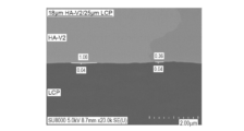
- Example 1 First, a liquid crystal polymer film (Vecstar CTQ, manufactured by Kuraray Co., Ltd.) having a thickness of 25 ⁇ m was prepared, and a rolled copper foil (HA-V2, manufactured by JX Metals Co., Ltd.) having a thickness of 18 ⁇ m was prepared as a metal foil. Next, after activating one surface of the liquid crystal polymer film by sputter etching with O 2 gas, a 5 nm NiCr alloy sputter layer was formed as an underlayer on the activated surface by sputtering, and a 10 nm thick NiCr alloy sputter layer was formed as an upper layer on the activated surface.
- a Cu sputter layer was formed by sputtering to form an intermediate layer (hereinafter also referred to as a Cu/NiCr alloy intermediate layer).
- an intermediate layer hereinafter also referred to as a Cu/NiCr alloy intermediate layer.
- the surface of the intermediate layer and the surface of the rolled copper foil are activated by sputter etching with Ar gas, and the activated surfaces of the intermediate layer and the rolled copper foil are roll-bonded with a line load of 1.5 tf/cm, A metal laminate was produced. The rolling reduction was 2.3%.
- the metal laminate material was heat-treated at 300° C. to obtain a metal laminate material of Example 1 (layer structure: rolled copper foil/intermediate layer/liquid crystal polymer film).
- Example 2 As the rolled copper foil, the metal laminate material of Example 2 (layer structure: rolled copper foil/intermediate layer/liquid crystal polymer film).
- Example 3 First, a liquid crystal polymer film (Vecstar CTQ, manufactured by Kuraray Co., Ltd.) having a thickness of 25 ⁇ m was prepared, and as the metal foil, the rolled copper foil used in Example 1 (HA-V2, manufactured by JX Metals Co., Ltd.) was prepared. Next, one surface of the liquid crystal polymer film is activated by sputter etching with O 2 gas, the surface of the rolled copper foil is activated by sputter etching with Ar gas, and the activated surfaces of the liquid crystal polymer film and the rolled copper foil are bonded together. A metal laminate was produced by roll-bonding with a linear load of 1.5 tf/cm. The rolling reduction was 2.3%. Next, the metal laminate material was heat-treated at 320° C. to obtain a metal laminate material (layer structure: rolled copper foil/liquid crystal polymer film) of Example 3.
- Vecstar CTQ manufactured by Kuraray Co., Ltd.
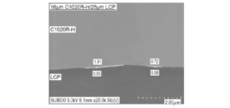
- Example 4 As the rolled copper foil, the metal laminate material of Example 4 was prepared in the same manner as in Example 3 except that the rolled copper foil used in Example 2 (C1020R-H manufactured by Sumitomo Mitsui Metal Mining Co., Ltd.) was used. layer structure: rolled copper foil/liquid crystal polymer film).
- Example 5 A metal laminate material of Example 5 (layer configuration: rolled copper foil/liquid crystal polymer film) was obtained in the same manner as in Example 4 except that a 50 ⁇ m-thick liquid crystal polymer film (Vecstar CTQ manufactured by Kuraray Co., Ltd.) was used. .
- Example 6 a liquid crystal polymer film having a thickness of 25 ⁇ m (Vecstar CTQ manufactured by Kuraray Co., Ltd.) was prepared, and a metal foil having a thickness of 1.5 ⁇ m was applied to a carrier layer made of copper having a thickness of 18 ⁇ m via a release layer (organic release layer). and a carrier-attached copper foil (MT18FL manufactured by Mitsui Mining & Smelting Co., Ltd.) having an ultra-thin copper layer and a roughened particle layer and an antirust layer on its surface.
- MT18FL manufactured by Mitsui Mining & Smelting Co., Ltd.
- Example 6 After one surface of the liquid crystal polymer film was activated by sputter etching with O 2 gas, a Cu/NiCr alloy intermediate layer was formed by sputtering in the same manner as in Example 1 on the activated surface. Next, the surface of the intermediate layer and the surface of the ultra-thin copper layer were activated by sputter etching with Ar gas, and the activated surfaces of the intermediate layer and the ultra-thin copper layer were roll-bonded with a linear load of 1.5 tf/cm. Then, a metal laminated material was produced. The rolling reduction was 3.4%. Next, the metal laminate material was heat-treated at 300° C. to obtain a metal laminate material of Example 6 (layer configuration: copper foil with carrier/intermediate layer/liquid crystal polymer film).
- Example 7 As the copper foil with a carrier, a carrier layer made of copper with a thickness of 18 ⁇ m is provided with an ultra-thin copper layer with a thickness of 2 ⁇ m via a peeling layer (inorganic peeling layer) and a rust prevention layer on the surface of the copper foil with a carrier ( A metal laminate of Example 7 (layer configuration: copper foil with carrier/intermediate layer/liquid crystal polymer film) was obtained in the same manner as in Example 6 except that prototype material A) was used.
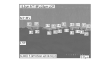
- Example 8 First, a liquid crystal polymer film (Vecstar CTQ, manufactured by Kuraray Co., Ltd.) having a thickness of 25 ⁇ m was prepared, and the copper foil with carrier used in Example 6 (MT18FL, manufactured by Mitsui Kinzoku Mining Co., Ltd.) was prepared as the metal foil. Next, one surface of the liquid crystal polymer film is activated by sputter etching with O 2 gas, the surface of the ultra-thin copper layer of the copper foil with a carrier is activated by sputter etching with Ar gas, and the liquid crystal polymer film and the ultra-thin copper layer are activated. The activated surfaces were roll-bonded with a linear load of 1.5 tf/cm to produce a metal laminate. The rolling reduction was 3.4%. Next, the metal laminate material was heat-treated at 300° C. to obtain a metal laminate material of Example 8 (layer configuration: copper foil with carrier/liquid crystal polymer film).
- MT18FL manufactured by Mitsui Kinzoku Mining Co., Ltd
- Example 9 As a copper foil with a carrier, a carrier layer made of copper with a thickness of 18 ⁇ m was provided with an ultrathin copper layer with a thickness of 2 ⁇ m via a peeling layer (organic peeling layer), and a roughened particle layer and an antirust layer were provided on the surface thereof.
- a metal laminate material of Example 9 (layer structure: copper foil with carrier/liquid crystal polymer film) was obtained in the same manner as in Example 8 except that a copper foil with a carrier (MT18EX manufactured by Mitsui Kinzoku Mining Co., Ltd.) was used. .
- Example 10 As a copper foil with a carrier, a carrier layer made of copper and having a thickness of 18 ⁇ m was provided with an ultra-thin copper layer having a thickness of 5 ⁇ m via a peeling layer (organic peeling layer), and a roughened particle layer and an antirust layer were provided on the surface thereof.
- the metal laminate material of Example 10 (layer structure: copper foil with carrier/liquid crystal polymer film) was prepared in the same manner as in Example 8 except that the copper foil with carrier (MT18SD-H manufactured by Mitsui Mining & Smelting Co., Ltd.) was used. Obtained.
- Example 11 As the copper foil with carrier, the metal laminate material of Example 11 (layer structure: copper foil with carrier / A liquid crystal polymer film) was obtained.
- Example 12 As a copper foil with a carrier, a carrier layer made of copper and having a thickness of 18 ⁇ m is provided with an ultrathin copper layer having a thickness of 1.5 ⁇ m via a peeling layer (organic peeling layer), and a roughened particle layer and an antirust layer are provided on the surface thereof.
- the metal laminate material of Example 12 (layer structure: copper foil with carrier/liquid crystal polymer film) was prepared in the same manner as in Example 8 except that the carrier-attached copper foil (manufactured by Mitsui Mining & Smelting Co., Ltd. MT18GN) was used. Obtained.
- Example 13 As a copper foil with a carrier, a carrier layer made of copper with a thickness of 18 ⁇ m was provided with an ultrathin copper layer with a thickness of 2 ⁇ m via a peeling layer (inorganic peeling layer), and a roughened particle layer and an antirust layer were provided on the surface thereof.
- a copper foil with a carrier (FUTF-7DAF-5 manufactured by Fukuda Metal Foil & Powder Co., Ltd.) was used, the metal laminate material of Example 13 (layer structure: copper foil with a carrier / liquid crystal polymer film) was obtained.
- Example 14 A 50 ⁇ m thick liquid crystal polymer film (Vecstar CTQ manufactured by Kuraray Co., Ltd.) is prepared, and a 12 ⁇ m thick electrolytic copper foil made of copper (CF-T9DA-SV manufactured by Fukuda Metal Foil & Powder Co., Ltd.) is prepared as a metal foil. bottom. Next, one surface of the liquid crystal polymer film is activated by sputter etching with O 2 gas, the surface of the electrolytic copper foil is activated by sputter etching with Ar gas, and the activated surfaces of the liquid crystal polymer film and the electrolytic copper foil are bonded together. A metal laminate was produced by roll-bonding with a linear load of 1.5 tf/cm. The rolling reduction was 2.3%. Next, the metal laminate material was heat-treated at 320° C. to obtain a metal laminate material of Example 14 (layer structure: electrolytic copper foil/liquid crystal polymer film).
- Example 15 As the electrolytic copper foil, the metal laminated material (layer Structure: electrolytic copper foil/liquid crystal polymer film) was obtained.
- Example 16 A 25 ⁇ m thick liquid crystal polymer film (Vecstar CTQ manufactured by Kuraray Co., Ltd.) is used, and an 18 ⁇ m thick electrolytic copper foil made of copper (CF-V9S-SV manufactured by Fukuda Metal Foil & Powder Co., Ltd.) is used as an electrolytic copper foil.
- a metal laminate material (layer structure: electrolytic copper foil/liquid crystal polymer film) of Example 16 was obtained in the same manner as in Example 14 except that
- Comparative example 1 By a heat lamination method, a 18 ⁇ m thick rolled copper foil having a treated layer consisting of a roughened particle layer etc. on one side is applied to both surfaces of a 50 ⁇ m thick liquid crystal polymer film (Vecstar CTQ manufactured by Kuraray Co., Ltd.) at 310 ° C. or higher.
- a metal laminate material of Comparative Example 1 (layer structure: rolled copper foil (with roughening treatment)/liquid crystal polymer film/rolled copper foil (with roughening treatment)) was produced by thermocompression bonding at a temperature of .
- Comparative example 2 As the rolled copper foil, a metal laminate material of Comparative Example 2 (layer structure: electrolytic copper foil/liquid crystal polymer film/electrolytic copper foil).
- FIGS. 6 to 13 show cross-sectional photographs of the metal laminate materials of Examples 1 to 4, 6 to 8, and 14, respectively
- FIGS. 2 shows a cross-sectional photograph of the metal laminate material No. 2.
- the following properties were evaluated for the metal laminates of Examples 1 to 16 and Comparative Examples 1 and 2.
- a cross-sectional photograph (Fig. 8) of the metal laminated material of Example 3 will be used.
- FIG. 8 on the surface of the copper foil (HA-V2 in FIG. 8) on the liquid crystal polymer film (LCP in FIG. 8) side, two points where the convex portions of the copper foil start are connected.
- the average value of b/a is obtained, and further, considering the variation of the values, the average value of b/a + 3 ⁇ (where ⁇ is the standard of b/a deviation) was obtained.
- FIG. 12 a cross-sectional photograph (FIG. 12) of the metal laminated material of Example 8.
- the convex portion of the copper foil (ultra-thin copper layer) Measure the width a of the convex portion, which is the length of the straight line connecting the two points where Then, the average value of b/a + 3 ⁇ was obtained.
- Transmission loss (S21) In order to evaluate the high-frequency transmission characteristics of the metal laminates of Example 5 and Comparative Example 2, transmission loss (S21) was measured. Since Example 5 is a single-sided material, a copper layer is provided by electroless copper plating on the exposed surface of the liquid crystal polymer film on the opposite side to which the rolled copper foil is laminated, and after making through holes, electrolytic copper plating is performed. , a sample for measurement with a copper layer (25 ⁇ m) on both sides was obtained. In the metal laminate material of Comparative Example 2, a sample for measurement having copper layers (25 ⁇ m) on both sides was obtained by performing electrolytic copper plating after forming through holes.
- the transmission line was a single-ended wiring of a microstrip transmission line, with a wiring height of 25 ⁇ m, a wiring width of 110 ⁇ m, and a wiring length of 100 mm. Measurement was performed at a frequency of 40 GHz using a network analyzer E8363B (manufactured by Keysight Technologies). In addition, in Example 5, a microstrip line was formed on the side of the laminated rolled copper foil and measured.
- Table 1 shows the structures and evaluation results of the metal laminate materials of Examples 1 to 16 and Comparative Examples 1 and 2.
- LCP means a liquid crystal polymer film.
- the metal laminate material of Example 5 in which the average value of b/a of the protrusions + 3 ⁇ is smaller and the surface of the copper foil is smooth, is superior to the comparison Compared with the metal laminated material of Example 2, the transmission loss (S21) at high frequencies was small, indicating excellent high-frequency characteristics. In general, transmission loss can be suppressed when the surface of the metal foil of the metal laminate is smooth, so the metal laminates of Examples 1 to 4 and 6 to 16 are the same as the metal laminate of Example 5. It is presumed to be excellent in high-frequency transmission characteristics.
- the metal laminated materials of Examples 1 to 16 are compared with the metal laminated materials of Comparative Examples 1 and 2. Although the surface was smooth, the peel strength was the same or higher. This is because in the metal laminate materials of Examples 1 to 16, a strong bond is formed at the interface between the liquid crystal polymer film and the copper foil by the surface activation treatment, so the roughening particles do not rely on the physical anchor effect. It is considered that this is because the adhesiveness of the lamination interface can be ensured.
- the metal laminates of Examples 1 to 16 produced by the surface activation bonding method are compared with the metal laminates of Comparative Examples 1 and 2 produced by the thermal lamination method, the metal layer and the liquid crystal polymer film It was shown that the peel strength of the metal foil is equal to or higher than that of the metal foil, and that the metal foil has a smoother surface and therefore has excellent high-frequency characteristics.
- Metal Laminate with Intermediate Layer O 2 gas, Ar gas and N 2 gas were used as gases for sputter etching of the liquid crystal polymer film.
- O 2 gas the metal laminate material of Example 2 was used.
- Example 17 A metal laminate of Example 17 was obtained in the same manner as in Example 2, except that Ar gas was used as the gas for sputter etching the liquid crystal polymer film.
- Example 18 A metal laminate of Example 18 was obtained in the same manner as in Example 2, except that N 2 gas was used as the gas for sputter etching the liquid crystal polymer film.
- Metal Laminated Material without Intermediate Layer O 2 gas, Ar gas and N 2 gas were used as gases for sputter etching of the liquid crystal polymer film.
- O 2 gas the metal laminate material of Example 4 was used.
- Comparative Example 3 A metal laminate of Comparative Example 3 was obtained in the same manner as in Example 4, except that Ar gas was used as the gas for sputter etching the liquid crystal polymer film.
- Comparative Example 4 A metal laminate of Comparative Example 4 was obtained in the same manner as in Example 4, except that N 2 gas was used as the gas for sputter etching the liquid crystal polymer film.
- the peel strength between the liquid crystal polymer film and the metal layer of the produced metal laminate was measured as described above. As a result, for the metal laminate having an intermediate layer, the peel strength was 8.2 N/cm for Example 2 (O 2 gas), 5.4 N/cm for Example 17 (Ar gas), and 5.4 N/cm for Example 18 ( N 2 gas) was 7.9 N/cm. In addition, for the metal laminates having no intermediate layer, the peel strength was 7.6 N/cm in Example 4 (O 2 gas), 1.0 N/cm in Comparative Example 3 (Ar gas), and 4 ( N2 gas) was 2.2 N/cm.
- the peel strength tends to be higher than when Ar gas and N 2 gas are used.
- the improvement in peel strength for the laminate was greater than for the metal laminate with an intermediate layer.
Abstract
The purpose of the present invention is to provide a metal laminate that exhibits both high cycle characteristics and high adhesiveness at a lamination interface. The present invention relates to: a metal laminate in which a metal layer formed from at least one metal-foil-including layer is laminated on at least one surface of a low-dielectric film, a plurality of protrusions of the metal foil being formed on the low-dielectric-film-side surface of the metal foil, and the sum of the average value of b/a and 3σ (in this expression, σ is the standard deviation of b/a) being 2.5 or less, where a is the width of the protrusions and b is the height of the protrusions, and the peel strength of the metal layer with respect to the low-dielectric film is 3N/cm or greater; a method for manufacturing the metal laminate; and a printed wiring board.
Description
本発明は、金属積層材及びその製造方法、並びにプリント配線板に関する。
The present invention relates to a metal laminated material, a method for manufacturing the same, and a printed wiring board.
従来、プリント配線板作製用の基材として、低誘電性フィルムに銅箔等の金属箔を積層させた金属積層材が知られている。近年、第5世代移動通信システム(5G)のサービスが各国において開始されており、5Gでの周波数帯、つまり高周波特性に優れた金属積層材が求められている。
Conventionally, as a substrate for producing printed wiring boards, a metal laminate material in which a metal foil such as a copper foil is laminated on a low-dielectric film is known. In recent years, 5th generation mobile communication system (5G) services have started in various countries, and there is a demand for laminated metal materials that are excellent in the frequency band of 5G, that is, in high-frequency characteristics.
金属積層材としては、一般的には、低誘電性フィルムに対する密着性の観点から、圧着面を粗面化した金属箔を加熱圧着する熱ラミネート法を用いて作製されるものが知られている。一般的に、熱ラミネート法では、表面に粗化処理を施した金属箔を用い、低誘電性フィルムを融点付近まで昇温して軟化させ、金属箔表面の粗化粒子を低誘電性フィルム内部に深く埋没させて、いわゆるアンカー効果によって密着性を確保している。
As a metal laminated material, it is generally known that from the viewpoint of adhesion to a low-dielectric film, a metal foil having a roughened bonding surface is thermally and compression-bonded by a thermal lamination method. . Generally, in the thermal lamination method, a metal foil with a roughened surface is used, and the low-dielectric film is softened by raising the temperature to near the melting point, and the roughened particles on the metal foil surface are removed from the inside of the low-dielectric film. It is deeply buried in the surface, and the adhesion is secured by the so-called anchor effect.
特許文献1には、表面に粗化処理を施した表面処理銅箔、該銅箔を絶縁基板に積層させた銅張積層板、及び該銅張積層板を用いたプリント配線板が開示されており、銅張積層板は熱ラミネート法により作製することができることが開示されている。
Patent Document 1 discloses a surface-treated copper foil having a roughened surface, a copper-clad laminate obtained by laminating the copper foil on an insulating substrate, and a printed wiring board using the copper-clad laminate. and discloses that the copper-clad laminate can be produced by a thermal lamination method.
ここで、高周波帯域での使用においては、金属積層材の金属箔の表面は平滑な方が伝送特性に優れることが知られている。熱ラミネート法により作製された従来の金属積層材では、金属箔表面を粗面化してアンカー効果により密着性を確保できるものの、粗面化した積層界面においては、高周波帯域で表皮効果による伝送特性の劣化が生じてしまい、高周波帯域における使用には十分に有用ではない。
Here, when used in a high frequency band, it is known that the smoother the surface of the metal foil of the metal laminated material, the better the transmission characteristics. In the conventional metal laminated material produced by the thermal lamination method, the surface of the metal foil is roughened to ensure adhesion due to the anchor effect. Degradation occurs and it is not useful enough for use in high frequency bands.
前記のように、熱ラミネート法により作製された従来の金属積層材では、金属箔表面を粗面化することにより、積層界面の密着性は確保されるものの、高周波特性が十分ではない場合があった。そこで本発明は、高周波特性及び積層界面の密着性を両立した金属積層材を提供することを目的とする。
As described above, in the conventional metal laminated material produced by the thermal lamination method, the adhesion of the laminated interface is ensured by roughening the surface of the metal foil, but the high-frequency characteristics may not be sufficient. rice field. SUMMARY OF THE INVENTION Accordingly, an object of the present invention is to provide a metal laminated material that achieves both high-frequency characteristics and adhesion at the interface between layers.
本発明者らは、前記課題を解決するため鋭意検討を行った結果、表面活性化接合法により金属積層材を作製することにより、金属箔をその表面の平滑性を維持したまま低誘電性フィルムに積層することができ、高周波特性及び積層界面の密着性を両立することができることを見出し、発明を完成した。すなわち、本発明の要旨は以下の通りである。
(1)低誘電性フィルムの少なくとも一方の面に、金属箔を含む少なくとも1層からなる金属層が積層された金属積層材であって、前記金属箔の前記低誘電性フィルムの側の表面に前記金属箔の複数の凸部が形成されており、前記凸部の幅をaとし、前記凸部の高さをbとしたとき、b/aの平均値+3σ(式中、σはb/aの標準偏差である)が2.5以下であり、且つ前記低誘電性フィルムと前記金属層のピール強度が3N/cm以上である、金属積層材。
(2)前記金属層が、前記低誘電性フィルムと前記金属箔との間に、銅、ニッケル、クロム又はその合金からなるスパッタ層を有していない、前記(1)に記載の金属積層材。
(3)前記金属箔が、圧延銅箔、キャリア付銅箔又は電解銅箔である、前記(1)又は(2)に記載の金属積層材。
(4)低誘電性フィルムの少なくとも一方の面に、金属箔を含む少なくとも1層からなる金属層が積層された金属積層材の製造方法であって、
前記金属箔の前記低誘電性フィルムの側の表面に前記金属箔の複数の凸部が形成されており、前記凸部の幅をaとし、前記凸部の高さをbとしたとき、b/aの平均値+3σ(式中、σはb/aの標準偏差である)が2.5以下であり、且つ前記低誘電性フィルムと前記金属層のピール強度が3N/cm以上であり、
該方法が、
低誘電性フィルムと金属箔とを準備する工程と、
前記低誘電性フィルムの少なくとも一方の表面をスパッタエッチングにより活性化する工程と、
前記金属箔の表面をスパッタエッチングにより活性化する工程と、
前記低誘電性フィルム及び前記金属箔の活性化した表面同士を0~30%の圧下率で圧延接合する工程と
を含む、金属積層材の製造方法。
(5)低誘電性フィルムの少なくとも一方の面に、金属箔を含む少なくとも1層からなる金属層が積層された金属積層材の製造方法であって、
前記金属層が、前記低誘電性フィルムと前記金属箔との間に金属を含む中間層を有し、
前記金属箔の前記低誘電性フィルムの側の表面に前記金属箔の複数の凸部が形成されており、前記凸部の幅をaとし、前記凸部の高さをbとしたとき、b/aの平均値+3σ(式中、σはb/aの標準偏差である)が2.5以下であり、且つ前記低誘電性フィルムと前記金属層のピール強度が3N/cm以上であり、
該方法が、
低誘電性フィルムと金属箔とを準備する工程と、
前記低誘電性フィルムの少なくとも一方の表面をスパッタエッチングにより活性化する工程と、
前記低誘電性フィルムの活性化した表面上に金属を含む中間層を形成する工程と、
前記中間層の表面をスパッタエッチングにより活性化する工程と、
前記金属箔の表面をスパッタエッチングにより活性化する工程と、
前記中間層及び前記金属箔の活性化した表面同士を0~30%の圧下率で圧延接合する工程と
を含む、金属積層材の製造方法。
(6)前記金属層が、前記低誘電性フィルムと前記金属箔との間に、銅、ニッケル、クロム又はその合金からなるスパッタ層を有していない、前記(4)に記載の金属積層材の製造方法。
(7)前記金属箔が、圧延銅箔、キャリア付銅箔又は電解銅箔である、前記(4)~(6)のいずれかに記載の金属積層材の製造方法。
(8)前記低誘電性フィルムの少なくとも一方の表面を酸素によるスパッタエッチングにより活性化する、前記(4)~(6)のいずれかに記載の金属積層材の製造方法。
(9)前記圧延接合する工程の温度が15℃以上100℃以下である、前記(4)~(6)のいずれかに記載の金属積層材の製造方法。
(10)圧延接合を行った後、前記低誘電性フィルムの融点-150℃以上前記融点+10℃以下の温度で熱処理を行う、前記(4)~(6)のいずれかに記載の金属積層材の製造方法。
(11)前記(1)~(3)のいずれかに記載の金属積層材に回路が形成されてなるプリント配線板。
本明細書は本願の優先権の基礎となる日本国特許出願番号2021-174667号の開示内容を包含する。 As a result of intensive studies to solve the above problems, the present inventors have found that by producing a metal laminated material by the surface activation bonding method, the metal foil can be a low dielectric film while maintaining the smoothness of the surface. The present inventors have found that it is possible to laminate a layer on the same layer, and that both high-frequency characteristics and adhesion at the interface of the layer can be achieved, and the invention has been completed. That is, the gist of the present invention is as follows.
(1) A metal laminate material in which at least one metal layer including a metal foil is laminated on at least one surface of a low dielectric film, wherein the surface of the metal foil on the low dielectric film side A plurality of convex portions are formed on the metal foil, and when the width of the convex portion is a and the height of the convex portion is b, the average value of b/a + 3σ (where σ is b/ a) is 2.5 or less, and the peel strength between the low dielectric film and the metal layer is 3 N/cm or more.
(2) The metal laminate material according to (1) above, wherein the metal layer does not have a sputtered layer made of copper, nickel, chromium, or an alloy thereof between the low dielectric film and the metal foil. .
(3) The metal laminate material according to (1) or (2) above, wherein the metal foil is a rolled copper foil, a copper foil with a carrier, or an electrolytic copper foil.
(4) A method for producing a laminated metal material in which at least one metal layer containing a metal foil is laminated on at least one surface of a low dielectric film,
A plurality of protrusions of the metal foil is formed on the surface of the metal foil on the low dielectric film side, and when the width of the protrusion is a and the height of the protrusion is b, b The average value of /a + 3σ (where σ is the standard deviation of b/a) is 2.5 or less, and the peel strength of the low dielectric film and the metal layer is 3 N / cm or more,
the method comprising:
providing a low dielectric film and a metal foil;
activating at least one surface of the low dielectric film by sputter etching;
activating the surface of the metal foil by sputter etching;
and a step of roll-bonding the activated surfaces of the low dielectric film and the metal foil with a rolling reduction of 0 to 30%.
(5) A method for producing a metal laminate material in which at least one metal layer containing a metal foil is laminated on at least one surface of a low dielectric film,
the metal layer has an intermediate layer containing a metal between the low dielectric film and the metal foil;
A plurality of protrusions of the metal foil is formed on the surface of the metal foil on the low dielectric film side, and when the width of the protrusion is a and the height of the protrusion is b, b The average value of /a + 3σ (where σ is the standard deviation of b/a) is 2.5 or less, and the peel strength of the low dielectric film and the metal layer is 3 N / cm or more,
the method comprising:
providing a low dielectric film and a metal foil;
activating at least one surface of the low dielectric film by sputter etching;
forming an intermediate layer comprising a metal on the activated surface of the low dielectric film;
activating the surface of the intermediate layer by sputter etching;
activating the surface of the metal foil by sputter etching;
and a step of roll-bonding the activated surfaces of the intermediate layer and the metal foil with a rolling reduction of 0 to 30%.
(6) The metal laminate material according to (4) above, wherein the metal layer does not have a sputtered layer made of copper, nickel, chromium, or an alloy thereof between the low dielectric film and the metal foil. manufacturing method.
(7) The method for producing a laminated metal material according to any one of (4) to (6) above, wherein the metal foil is a rolled copper foil, a copper foil with a carrier, or an electrolytic copper foil.
(8) The method for producing a metal laminate material according to any one of (4) to (6) above, wherein at least one surface of the low dielectric film is activated by sputter etching with oxygen.
(9) The method for producing a laminated metal material according to any one of (4) to (6) above, wherein the temperature in the roll-bonding step is 15° C. or higher and 100° C. or lower.
(10) The metal laminate material according to any one of (4) to (6), wherein heat treatment is performed at a temperature of −150° C. or more and +10° C. or less of the melting point of the low dielectric film after the roll bonding. manufacturing method.
(11) A printed wiring board in which a circuit is formed on the metal laminate material according to any one of (1) to (3) above.
This specification includes the disclosure content of Japanese Patent Application No. 2021-174667, which is the basis of priority of this application.
本発明によれば、高周波特性及び積層界面の密着性を両立した金属積層材を提供することができる。
According to the present invention, it is possible to provide a metal laminated material that achieves both high-frequency characteristics and adhesion at the interface of the laminate.
以下、本発明を詳細に説明する。本発明は、低誘電性フィルムの少なくとも一方の面に、金属箔を含む少なくとも1層からなる金属層が積層された金属積層材に関する。本発明の金属積層材は、低誘電性フィルムの一方の面に金属層が積層されたもの、及び低誘電性フィルムの両方の面に金属層が積層されたものを含む。本発明の金属積層材は、金属箔の低誘電性フィルムの側の表面が平滑であるため、金属積層材が高周波特性に優れ、且つ低誘電性フィルムと金属層が十分な密着性を有するものである。
The present invention will be described in detail below. TECHNICAL FIELD The present invention relates to a laminated metal material in which at least one metal layer including a metal foil is laminated on at least one surface of a low dielectric film. The metal laminate of the present invention includes a low dielectric film laminated with a metal layer on one side and a low dielectric film laminated with a metal layer on both sides. In the metal laminate material of the present invention, since the surface of the metal foil on the low dielectric film side is smooth, the metal laminate material has excellent high-frequency characteristics, and the low dielectric film and the metal layer have sufficient adhesion. is.
A.金属積層材
まず、本発明の第1実施形態の金属積層材について以下に説明する。 A. Metal Laminated Material First, the metal laminated material of the first embodiment of the present invention will be described below.
まず、本発明の第1実施形態の金属積層材について以下に説明する。 A. Metal Laminated Material First, the metal laminated material of the first embodiment of the present invention will be described below.
図1は、本発明の第1実施形態の一態様の金属積層材を示す概略断面図である。図1に示すように、第1実施形態の金属積層材1Aは、低誘電性フィルム20の一方の表面に金属箔からなる金属層10が積層されている。
FIG. 1 is a schematic cross-sectional view showing a laminated metal material according to one aspect of the first embodiment of the present invention. As shown in FIG. 1, in the metal laminated material 1A of the first embodiment, a metal layer 10 made of metal foil is laminated on one surface of a low dielectric film 20 .
図2は、本発明の第1実施形態の別の態様の金属積層材を示す概略断面図である。この態様においては、金属箔として、極薄金属層、剥離層、及びキャリア層を有するキャリア付金属箔が用いられている。図2に示すように、本発明の金属積層材1Bは、低誘電性フィルム20の一方の表面に、キャリア付金属箔からなる金属層10が積層されている。金属層10は、低誘電性フィルム20側から、極薄金属層14、剥離層13、及びキャリア層12の順番になるように積層されている。
FIG. 2 is a schematic cross-sectional view showing another aspect of the metal laminate material of the first embodiment of the present invention. In this aspect, a metal foil with a carrier having an ultra-thin metal layer, a release layer, and a carrier layer is used as the metal foil. As shown in FIG. 2, in the metal laminate 1B of the present invention, a metal layer 10 made of a metal foil with a carrier is laminated on one surface of a low dielectric film 20 . The metal layer 10 is laminated in order of the ultra-thin metal layer 14, the release layer 13, and the carrier layer 12 from the low dielectric film 20 side.
以下に、本発明の第1実施形態の金属積層材の各構成について詳細に説明する。
Below, each configuration of the metal laminate material of the first embodiment of the present invention will be described in detail.
1.低誘電性フィルム
低誘電性フィルムの材質としては、フレキシブル基板として用い得る低誘電性のポリマー材料であれば適用可能であり、例えば、比誘電率εrが3.3以下、誘電正接tanδの値が0.006以下であるような材料であるが、これに限定されなくても良い。具体的には、液晶ポリマー、ポリフッ化エチレン(ポリテトラフルオロエチレン等のフッ素系樹脂)、ポリアミド、イソシアネート化合物、ポリアミドイミド、ポリイミド、低誘電率ポリイミド、ポリエチレンテレフタレート、ポリエーテルイミド、シクロオレフィンポリマー等の材料から適宜選択して用いることができる。好ましくは、液晶ポリマー、ポリフッ化エチレン、ポリアミド又は低誘電率ポリイミドであり、より好ましくは液晶ポリマーである。低誘電性フィルムは、単層のフィルムであるか、又は複数層からなる積層体であり、複数層である場合は、その複数層のうちのいずれか1層以上が上記の低誘電性のポリマー材料からなる層であれば良い。低誘電性のポリマー材料からなる層以外の層は、エポキシ樹脂等の従来知られた種々の材料から構成することができる。なお、液晶ポリマーとは、溶融状態で液晶の性質を示すような、パラヒドロキシ安息香酸等を基本構造とする芳香族ポリエステル系樹脂をいう。 1. Low-dielectric film As the material of the low-dielectric film, any low-dielectric polymer material that can be used as a flexible substrate can be applied . is 0.006 or less, but it is not limited to this. Specifically, liquid crystal polymer, polyfluoroethylene (fluorinated resin such as polytetrafluoroethylene), polyamide, isocyanate compound, polyamideimide, polyimide, low dielectric constant polyimide, polyethylene terephthalate, polyetherimide, cycloolefin polymer, etc. The material can be appropriately selected and used. Liquid crystal polymer, polyethylene fluoride, polyamide or low dielectric constant polyimide is preferred, and liquid crystal polymer is more preferred. The low dielectric film is a single layer film or a laminate consisting of multiple layers, and in the case of multiple layers, any one or more of the multiple layers is the above low dielectric polymer Any layer made of material may be used. Layers other than the layer of low-dielectric polymer material can be composed of various conventionally known materials such as epoxy resin. The term "liquid crystal polymer" refers to an aromatic polyester resin having a basic structure of parahydroxybenzoic acid or the like, which exhibits liquid crystal properties in a molten state.
低誘電性フィルムの材質としては、フレキシブル基板として用い得る低誘電性のポリマー材料であれば適用可能であり、例えば、比誘電率εrが3.3以下、誘電正接tanδの値が0.006以下であるような材料であるが、これに限定されなくても良い。具体的には、液晶ポリマー、ポリフッ化エチレン(ポリテトラフルオロエチレン等のフッ素系樹脂)、ポリアミド、イソシアネート化合物、ポリアミドイミド、ポリイミド、低誘電率ポリイミド、ポリエチレンテレフタレート、ポリエーテルイミド、シクロオレフィンポリマー等の材料から適宜選択して用いることができる。好ましくは、液晶ポリマー、ポリフッ化エチレン、ポリアミド又は低誘電率ポリイミドであり、より好ましくは液晶ポリマーである。低誘電性フィルムは、単層のフィルムであるか、又は複数層からなる積層体であり、複数層である場合は、その複数層のうちのいずれか1層以上が上記の低誘電性のポリマー材料からなる層であれば良い。低誘電性のポリマー材料からなる層以外の層は、エポキシ樹脂等の従来知られた種々の材料から構成することができる。なお、液晶ポリマーとは、溶融状態で液晶の性質を示すような、パラヒドロキシ安息香酸等を基本構造とする芳香族ポリエステル系樹脂をいう。 1. Low-dielectric film As the material of the low-dielectric film, any low-dielectric polymer material that can be used as a flexible substrate can be applied . is 0.006 or less, but it is not limited to this. Specifically, liquid crystal polymer, polyfluoroethylene (fluorinated resin such as polytetrafluoroethylene), polyamide, isocyanate compound, polyamideimide, polyimide, low dielectric constant polyimide, polyethylene terephthalate, polyetherimide, cycloolefin polymer, etc. The material can be appropriately selected and used. Liquid crystal polymer, polyethylene fluoride, polyamide or low dielectric constant polyimide is preferred, and liquid crystal polymer is more preferred. The low dielectric film is a single layer film or a laminate consisting of multiple layers, and in the case of multiple layers, any one or more of the multiple layers is the above low dielectric polymer Any layer made of material may be used. Layers other than the layer of low-dielectric polymer material can be composed of various conventionally known materials such as epoxy resin. The term "liquid crystal polymer" refers to an aromatic polyester resin having a basic structure of parahydroxybenzoic acid or the like, which exhibits liquid crystal properties in a molten state.
低誘電性フィルムの厚みは、金属積層材の用途等に応じて適宜設定することができる。例えば、フレキシブルなプリント配線板として用いる場合は、厚みは通常10μm以上150μm以下であり、好ましくは10μm以上100μm以下であり、より好ましくは10μm以上75μm以下であり、特に好ましくは10μm以上50μm以下である。低誘電性フィルムの厚みは、金属積層材の断面の光学顕微鏡写真を取得し、その光学顕微鏡写真において任意の10点における低誘電性フィルムの厚みを計測し、得られた値の平均値をいう。なお、接合前の低誘電性フィルムの厚みは、マイクロメータ等によって測定可能であり、対象とする低誘電性フィルムの表面上からランダムに選択した10点において測定した厚みの平均値をいう。また、用いる低誘電性フィルムについては、10点の測定値の平均値からの偏差が全ての測定値で20%以内であることが好ましく、より好ましくは10%以内である。
The thickness of the low-dielectric film can be appropriately set according to the application of the metal laminated material. For example, when used as a flexible printed wiring board, the thickness is usually 10 μm or more and 150 μm or less, preferably 10 μm or more and 100 μm or less, more preferably 10 μm or more and 75 μm or less, and particularly preferably 10 μm or more and 50 μm or less. . The thickness of the low dielectric film is the average value of the obtained values obtained by obtaining an optical micrograph of the cross section of the metal laminate, measuring the thickness of the low dielectric film at arbitrary 10 points in the optical micrograph. . The thickness of the low dielectric film before bonding can be measured with a micrometer or the like, and refers to the average thickness measured at 10 randomly selected points on the surface of the target low dielectric film. Further, with respect to the low dielectric film to be used, the deviation from the average value of 10 measured values is preferably within 20%, more preferably within 10% for all measured values.
2.金属層
金属層は、金属箔を含むものであれば特に限定されず、当該金属箔からなるものでも良いし、当該金属箔に加え、他の層をさらに有するものでも良い。金属層が他の層を有する場合、低誘電性フィルムと金属箔との間に当該他の層を有することが好ましい。 2. Metal Layer The metal layer is not particularly limited as long as it contains a metal foil, and may consist of the metal foil, or may have other layers in addition to the metal foil. If the metal layer has other layers, it preferably has the other layers between the low dielectric film and the metal foil.
金属層は、金属箔を含むものであれば特に限定されず、当該金属箔からなるものでも良いし、当該金属箔に加え、他の層をさらに有するものでも良い。金属層が他の層を有する場合、低誘電性フィルムと金属箔との間に当該他の層を有することが好ましい。 2. Metal Layer The metal layer is not particularly limited as long as it contains a metal foil, and may consist of the metal foil, or may have other layers in addition to the metal foil. If the metal layer has other layers, it preferably has the other layers between the low dielectric film and the metal foil.
金属箔を構成する金属の種類は、金属積層材の用途により異なり特に限定されないが、例えば、銅、鉄、ニッケル、亜鉛、スズ、クロム、金、銀、白金、コバルト、チタン及びその合金が挙げられる。金属箔としては、中でも銅箔又は銅合金箔が好ましい。これらを低誘電性フィルムと圧延接合することで、例えば微細な配線形成用のフレキシブル基板を得ることができるからである。
The type of metal constituting the metal foil varies depending on the application of the metal laminate and is not particularly limited, but examples include copper, iron, nickel, zinc, tin, chromium, gold, silver, platinum, cobalt, titanium and alloys thereof. be done. As the metal foil, copper foil or copper alloy foil is particularly preferable. This is because, for example, a flexible substrate for forming fine wiring can be obtained by rolling and bonding these to a low dielectric film.
金属箔の厚みは、金属積層材の用途により異なり特に限定されないが、例えば、フレキシブルプリント配線基板用途であれば、3μm以上100μm以下が好ましく、中でも10μm以上50μm以下が好ましい。ここで、金属箔の厚みは、金属積層材の断面の光学顕微鏡写真を取得し、その光学顕微鏡写真において任意の10点における金属箔の厚みを計測し、得られた値の平均値をいう。
The thickness of the metal foil varies depending on the application of the metal laminated material and is not particularly limited. Here, the thickness of the metal foil refers to the average value of the values obtained by taking an optical micrograph of the cross section of the metal laminate, measuring the thickness of the metal foil at arbitrary 10 points in the optical micrograph.
金属箔は、好ましくは圧延金属箔、キャリア付金属箔又は電解金属箔であり、より好ましくは圧延銅箔、キャリア付銅箔又は電解銅箔である。また、金属箔は、単層箔であっても良く、これらの積層箔であっても良い。
The metal foil is preferably a rolled metal foil, a metal foil with a carrier or an electrolytic metal foil, more preferably a rolled copper foil, a copper foil with a carrier or an electrolytic copper foil. Also, the metal foil may be a single-layer foil or a laminated foil of these.
金属箔として圧延銅箔を用いる場合、圧延銅箔としては、特に限定されないが、例えば、JX金属(株)製HA-V2や三井住友金属鉱山伸銅(株)製C1020R-H等が挙げられる。また金属箔として電解銅箔を用いる場合、電解銅箔としては、特に限定されないが、例えば、福田金属箔粉工業(株)製CF-T9DA-SV、CF-V9S-SV、CF-PLFA等が挙げられる。
When a rolled copper foil is used as the metal foil, the rolled copper foil is not particularly limited. . When electrolytic copper foil is used as the metal foil, the electrolytic copper foil is not particularly limited. mentioned.
微細な配線形成用のフレキシブル基板を作製する場合は、金属箔として、極薄金属層、剥離層及びキャリア層を有するキャリア付金属箔を用いることが好ましい。キャリア付金属箔を使用する場合、図2に示すように、低誘電性フィルム側から極薄金属層、剥離層及びキャリア層の順番になるようにキャリア付金属箔を積層させる。キャリア付金属箔を用いる場合、得られる金属積層材における「金属箔」とは、極薄金属層、剥離層及びキャリア層からなる部分をいう。なお、金属積層材の製造方法において準備する金属箔としては、キャリア付金属箔の極薄金属層の表面に粗化粒子層や防錆層を有するものを用いても良い。
When producing a flexible substrate for forming fine wiring, it is preferable to use a metal foil with a carrier having an ultra-thin metal layer, a release layer and a carrier layer as the metal foil. When using a metal foil with a carrier, as shown in FIG. 2, the metal foil with a carrier is laminated in the order of an ultra-thin metal layer, a release layer and a carrier layer from the low dielectric film side. In the case of using a metal foil with a carrier, the "metal foil" in the resulting metal laminate refers to a portion composed of an ultra-thin metal layer, a release layer and a carrier layer. As the metal foil to be prepared in the method for producing a metal laminate, a metal foil with a carrier having a roughened particle layer or an antirust layer on the surface of an ultra-thin metal layer may be used.
キャリア付金属箔のキャリア層は、シート形状を有するものであり、金属積層材への皺や折れの発生、極薄金属層への傷を防止するための支持材料或いは保護層として機能する。キャリア層としては、銅、アルミニウム、ニッケル、及びその合金類(ステンレス、真鍮等)、表面に金属をコーティングした樹脂等からなる箔若しくは板状のものが挙げられる。キャリア層は、好ましくは銅箔である。キャリア層の厚みは、特に限定されないが、例えば10μm以上100μm以下である。
The carrier layer of the metal foil with carrier has a sheet shape and functions as a supporting material or a protective layer to prevent wrinkles and creases in the metal laminate and damage to the ultra-thin metal layer. Examples of the carrier layer include a foil or plate-shaped layer made of copper, aluminum, nickel, alloys thereof (stainless steel, brass, etc.), resin coated with metal on the surface, or the like. The carrier layer is preferably copper foil. The thickness of the carrier layer is not particularly limited, but is, for example, 10 μm or more and 100 μm or less.
キャリア付金属箔の剥離層は、キャリア層の剥離強度を小さくし、さらに、熱処理によりキャリア層と極薄金属層の間で起こり得る相互拡散を抑制する機能も有する。剥離層は、有機系剥離層及び無機系剥離層のいずれであっても良く、有機系剥離層に用いられる成分としては、例えば、窒素含有有機化合物、硫黄含有有機化合物、カルボン酸等が挙げられる。窒素含有有機化合物としては、トリアゾール化合物、イミダゾール化合物等が挙げられる。トリアゾール化合物の例としては、1,2,3-ベンゾトリアゾール、カルボキシベンゾトリアゾール、N’,N’-ビス(ベンゾトリアゾリルメチル)ユリア、1H-1,2,4-トリアゾール及び3-アミノ-1H-1,2,4-トリアゾール等が挙げられる。硫黄含有有機化合物の例としては、メルカプトベンゾチアゾール、チオシアヌル酸、2-ベンズイミダゾールチオール等が挙げられる。カルボン酸の例としては、モノカルボン酸、ジカルボン酸等が挙げられる。また、無機系剥離層に用いられる成分としては、例えば、Ni、Mo、Co、Cr、Fe、Ti、W、P、Zn、クロメート処理膜等が挙げられる。剥離層の厚みは、通常1nm以上1μm以下であり、好ましくは5nm以上500nm以下である。
The peeling layer of the carrier-attached metal foil reduces the peeling strength of the carrier layer, and also has the function of suppressing interdiffusion that can occur between the carrier layer and the ultra-thin metal layer due to heat treatment. The release layer may be either an organic release layer or an inorganic release layer. Examples of components used in the organic release layer include nitrogen-containing organic compounds, sulfur-containing organic compounds, carboxylic acids, and the like. . Nitrogen-containing organic compounds include triazole compounds and imidazole compounds. Examples of triazole compounds include 1,2,3-benzotriazole, carboxybenzotriazole, N',N'-bis(benzotriazolylmethyl)urea, 1H-1,2,4-triazole and 3-amino- 1H-1,2,4-triazole and the like. Examples of sulfur-containing organic compounds include mercaptobenzothiazole, thiocyanuric acid, 2-benzimidazolethiol, and the like. Examples of carboxylic acids include monocarboxylic acids, dicarboxylic acids, and the like. Examples of components used for the inorganic release layer include Ni, Mo, Co, Cr, Fe, Ti, W, P, Zn, chromate treatment films, and the like. The thickness of the release layer is usually 1 nm or more and 1 μm or less, preferably 5 nm or more and 500 nm or less.
キャリア付金属箔の極薄金属層を構成する金属は、金属積層材の用途により異なり特に限定されないが、例えば、銅、鉄、ニッケル、亜鉛、スズ、クロム、金、銀、白金、コバルト、チタン及びその合金等が挙げられる。極薄金属層は、銅又は銅合金の層であることが好ましい。極薄金属層の厚みは、通常0.5μm以上10μm以下であり、好ましくは1μm以上7μm以下である。
The metal that constitutes the ultra-thin metal layer of the metal foil with carrier is not particularly limited depending on the application of the metal laminate, but examples include copper, iron, nickel, zinc, tin, chromium, gold, silver, platinum, cobalt, and titanium. and alloys thereof. The ultra-thin metal layer is preferably a copper or copper alloy layer. The thickness of the ultrathin metal layer is usually 0.5 μm or more and 10 μm or less, preferably 1 μm or more and 7 μm or less.
キャリア付金属箔としては、キャリア層及び極薄金属層が、銅又は銅合金であるものが好ましく、これらが銅であるキャリア付銅箔がより好ましい。キャリア付銅箔としては特に限定されないが、例えば、三井金属鉱業(株)製MT18FL、MT18GN、MT18EXやMT18SD-H等が挙げられる。
As for the metal foil with a carrier, the carrier layer and the ultra-thin metal layer are preferably made of copper or a copper alloy, more preferably a copper foil with a carrier in which these are copper. The carrier-attached copper foil is not particularly limited, but examples thereof include MT18FL, MT18GN, MT18EX and MT18SD-H manufactured by Mitsui Mining & Smelting Co., Ltd.
なお、金属層は、図1~2には記載していないが、金属箔の低誘電性フィルム側の表面に粗化粒子層、防錆層、耐熱層、及びシランカップリング剤による処理層等のうちの少なくとも一種の層(以下、「処理層」ということがある)をさらに有していても良い。処理層は、いずれか一種の層が積層されていても良いし、複数種の層が積層されていても良い。粗化粒子層は、例えば、Cu、Co及びNiからなる群より選択されるいずれか一種の金属又はその合金を含むことができるが、これに限定されなくても良い。具体的には、コバルト-ニッケル合金めっき層、銅-コバルト-ニッケル合金めっき層等が挙げられる。また、防錆層は、例えば、Cr、Ni及びZnからなる群より選択されるいずれか一種の金属又はその合金を含むことができるが、これに限定されなくても良い。具体的には、クロム酸化物の皮膜処理、クロム酸化物と亜鉛/亜鉛酸化物との混合物皮膜処理、Niめっき層等を挙げることができる。耐熱層においては、例えばCo、Ni及びMoからなる群より選択されるいずれか一種の金属又はその合金を含むことができるが、これに限定されなくても良い。さらに、シランカップリング剤としては、オレフィン系シラン、エポキシ系シラン、アクリル系シラン、アミノ系シラン、メルカプト系シランを挙げることができるが、これらに限定されるものではない。シランカップリング剤の塗布は、スプレーによる吹付け、コーターによる塗布、浸漬等の方法を適宜用いて行うことができる。なお、粗化粒子層、防錆層、及び耐熱層は、以下の第2実施形態の金属積層材について説明する中間層とは異なるものである。
Although not shown in FIGS. 1 and 2, the metal layer includes a roughened particle layer, an antirust layer, a heat-resistant layer, and a layer treated with a silane coupling agent on the surface of the metal foil on the low dielectric film side. You may further have at least 1 type of layer (it may be hereafter called a "treatment layer"). Any one type of layer may be laminated|stacked, and the process layer may be laminated|stacked with the layer of multiple types. The roughened particle layer may contain, for example, any one metal selected from the group consisting of Cu, Co and Ni, or an alloy thereof, but is not limited thereto. Specific examples include a cobalt-nickel alloy plated layer, a copper-cobalt-nickel alloy plated layer, and the like. Also, the antirust layer may contain, for example, any one type of metal selected from the group consisting of Cr, Ni and Zn, or an alloy thereof, but is not limited thereto. Specifically, chromium oxide film treatment, mixed film treatment of chromium oxide and zinc/zinc oxide, Ni plating layer, and the like can be mentioned. The heat-resistant layer may contain, for example, one kind of metal selected from the group consisting of Co, Ni and Mo, or an alloy thereof, but the material is not limited to this. Furthermore, silane coupling agents include, but are not limited to, olefinic silanes, epoxy silanes, acrylic silanes, amino silanes, and mercapto silanes. Application of the silane coupling agent can be carried out by appropriately using a method such as spraying, coating with a coater, or immersion. Note that the roughened particle layer, the antirust layer, and the heat resistant layer are different from the intermediate layer described below for the metal laminate of the second embodiment.
第1実施形態の金属積層材は、好ましくは、以下の第2実施形態の金属積層材について説明する中間層を有していない。金属積層材が中間層を有していないことにより、金属積層材の生産性が向上し、製造コストを低減することができる。好ましい実施形態において、本発明の金属積層材は、低誘電性フィルムと金属箔との間に、金属を含む中間層を有しておらず、好ましくは銅、ニッケル、クロム又はその合金からなるスパッタ層を有していない。中間層を有していない金属積層材の一実施形態において、低誘電性フィルムと金属箔(好ましくは圧延金属箔)が直接積層されている。また、中間層を有していない金属積層材の別の一実施形態において、低誘電性フィルムに、前記の粗化粒子層、及び/又は前記の防錆層が積層されており、金属箔(好ましくはキャリア付金属箔)がその上に積層されている。この態様の金属積層材において、具体的には、低誘電性フィルムに、Cu、Co及びNiからなる群より選択されるいずれか一種の金属又はその合金を含む粗化粒子層、及び/又はCr、Ni及びZnからなる群より選択されるいずれか一種の金属又はその合金を含む皮膜である防錆層が積層されており、キャリア付金属箔がその上に積層されている。
The metal laminate material of the first embodiment preferably does not have an intermediate layer, which is described below for the metal laminate material of the second embodiment. Since the metal laminate does not have an intermediate layer, the productivity of the metal laminate can be improved and the manufacturing cost can be reduced. In a preferred embodiment, the metal laminate of the present invention does not have an intermediate layer containing metal between the low dielectric film and the metal foil, and preferably consists of copper, nickel, chromium or alloys thereof. does not have layers. In one embodiment of the metal laminate with no interlayers, the low dielectric film and metal foil (preferably rolled metal foil) are directly laminated. In another embodiment of the metal laminate having no intermediate layer, the low dielectric film is laminated with the roughened particle layer and/or the antirust layer, and the metal foil ( A metal foil with a carrier) is laminated thereon. In the metal laminate material of this aspect, specifically, the low dielectric film includes a roughened particle layer containing any one metal selected from the group consisting of Cu, Co and Ni or an alloy thereof, and / or Cr , Ni and Zn.
次に、本発明の第2実施形態の金属積層材について以下に説明する。図3は、本発明の第2実施形態の一態様の金属積層材を示す概略断面図である。図3に示すように、本発明の金属積層材1Cは、低誘電性フィルム20の一方の表面に金属層10が積層されている。金属積層材1Cは、低誘電性フィルム20と金属箔11との間に金属を含む中間層15を有する。よって、金属層10は、低誘電性フィルム20の一方の表面に積層された金属を含む中間層15と、中間層15の低誘電性フィルム20側とは反対側の表面に積層された金属箔11とを有する。
Next, the metal laminate material of the second embodiment of the present invention will be described below. FIG. 3 is a schematic cross-sectional view showing a laminated metal material according to one aspect of the second embodiment of the present invention. As shown in FIG. 3, a metal laminate 1C of the present invention has a metal layer 10 laminated on one surface of a low dielectric film 20 . The metal laminated material 1</b>C has an intermediate layer 15 containing metal between the low dielectric film 20 and the metal foil 11 . Therefore, the metal layer 10 consists of an intermediate layer 15 containing metal laminated on one surface of the low dielectric film 20 and a metal foil laminated on the surface of the intermediate layer 15 opposite to the low dielectric film 20 side. 11.
図4は、本発明の第2実施形態の別の態様の金属積層材を示す概略断面図である。この態様においては、金属箔として、極薄金属層、剥離層、及びキャリア層を有するキャリア付金属箔が用いられている。図4に示すように、本発明の金属積層材1Dは、低誘電性フィルム20の一方の表面に金属層10が積層されている。金属積層材1Dは、低誘電性フィルム20と、極薄金属層14、剥離層13、及びキャリア層12を有する金属箔11との間に金属を含む中間層15を有する。よって、金属層10は、低誘電性フィルム20側から、中間層15、極薄金属層14、剥離層13、及びキャリア層12の順番になるように積層されている。
FIG. 4 is a schematic cross-sectional view showing another aspect of the metal laminate material of the second embodiment of the present invention. In this aspect, a metal foil with a carrier having an ultra-thin metal layer, a release layer, and a carrier layer is used as the metal foil. As shown in FIG. 4, a metal laminate 1D of the present invention has a metal layer 10 laminated on one surface of a low dielectric film 20 . The metal laminate 1D has an intermediate layer 15 containing metal between a low dielectric film 20 and a metal foil 11 having an ultra-thin metal layer 14, a release layer 13 and a carrier layer 12. FIG. Therefore, the metal layer 10 is laminated in order of the intermediate layer 15, the ultra-thin metal layer 14, the release layer 13, and the carrier layer 12 from the low dielectric film 20 side.
第2実施形態の金属積層材においては、中間層を設けることにより、金属箔又は低誘電性フィルムの表面を保護し、また金属箔と低誘電性フィルムとの密着性を向上することができる。中間層は、金属を含む層であれば特に限定されず、1層の金属を含む層でも良いし、2層以上の金属を含む層が積層されたものでも良い。中間層としては、低誘電性フィルム上に設けられた、スパッタ成膜、又は蒸着若しくは無電解めっきによる層が挙げられるが、好ましくはスパッタ成膜により形成される層(スパッタ層)である。中間層の有無は、金属積層材の金属箔と低誘電性フィルムの界面を走査電子顕微鏡或いは透過電子顕微鏡等(倍率20000倍以上)により分析することで判別することができる。
In the metal laminated material of the second embodiment, by providing the intermediate layer, it is possible to protect the surface of the metal foil or the low dielectric film and improve the adhesion between the metal foil and the low dielectric film. The intermediate layer is not particularly limited as long as it is a layer containing a metal, and may be a single layer containing a metal, or a laminate of two or more layers containing a metal. Examples of the intermediate layer include a layer provided on the low-dielectric film by sputtering, vapor deposition, or electroless plating, and preferably a layer formed by sputtering (sputter layer). The presence or absence of the intermediate layer can be determined by analyzing the interface between the metal foil of the metal laminate and the low-dielectric film with a scanning electron microscope, a transmission electron microscope, or the like (magnification of 20,000 times or more).
中間層は、金属を含むものであれば特に限定されないが、銅、鉄、ニッケル、亜鉛、クロム、コバルト、チタン、スズ、白金、銀、金、アルミニウム、パラジウム、及びジルコニウムからなる群より選択されるいずれか一種の金属又はその合金を含むものが好ましく、銅、ニッケル、クロム又はその合金を含むものがより好ましく、銅、銅とニッケルの合金、ニッケル又はニッケルとクロムの合金を含むものが特に好ましい。また、中間層は、金属を含む層が複数積層されたものでも良い。
The intermediate layer is not particularly limited as long as it contains metal, but is selected from the group consisting of copper, iron, nickel, zinc, chromium, cobalt, titanium, tin, platinum, silver, gold, aluminum, palladium, and zirconium. preferably contains any one of the metals or alloys thereof, more preferably copper, nickel, chromium or alloys thereof, especially those containing copper, alloys of copper and nickel, nickel or alloys of nickel and chromium preferable. Further, the intermediate layer may be formed by laminating a plurality of layers containing metal.
中間層は、好ましくは、低誘電性フィルムと金属箔との間に、スパッタ成膜により形成された、銅、ニッケル、クロム又はその合金からなるスパッタ層である。
The intermediate layer is preferably a sputtered layer of copper, nickel, chromium or alloys thereof formed by sputter deposition between the low dielectric film and the metal foil.
中間層の厚みは、密着性向上等の機能を発揮し得る厚みであれば良く、特に限定されないが、例えば、5nm以上200nm以下が好ましく、中でも10nm以上100nm以下が好ましい。
The thickness of the intermediate layer is not particularly limited as long as it can exhibit a function such as adhesion improvement.
第2実施形態の金属積層材について、他の構成については第1実施形態の金属積層材について前記の通りである。
Regarding the metal laminate material of the second embodiment, other configurations are as described above for the metal laminate material of the first embodiment.
本発明の金属積層材は、金属箔の積層界面に相当する低誘電性フィルム側の表面が平滑であるため、熱ラミネート法により作製された従来の金属積層材と比較して高周波特性に優れる。金属箔の表面には、通常、粗さやうねりなどによる凹凸形状が形成されている。本発明においては、金属箔表面の平滑性を、金属積層材の断面観察から算出される金属箔の凸部の幅と高さの比(以下、縦横比ということがある)を用いて評価した。表面の平滑性の指標としては、表面粗度が広く用いられている。表面粗度は、一般に、物体の表面形状を理想表面と比べたときの、鉛直方向の偏差の程度を計るものである。ここで、熱ラミネート法により作製された従来の金属積層材では、金属箔表面の粗化粒子が低誘電性フィルム内部に深く埋没しており、低誘電性フィルム内部には入り組んだ凹形状が形成されている。表面粗度の測定では、このような入り組んだ凹形状を正確に把握することができない。本発明では、金属積層材の断面観察から算出される凸部の縦横比を平滑性の指標として用いることにより、従来の金属積層材との適切な比較が可能となる。なお、金属箔表面の凸部は、材料として使用した金属箔に由来するものであり、金属箔に他の要素を加えることによって形成されるものではない。
The metal laminate material of the present invention has a smooth surface on the low-dielectric film side, which corresponds to the interface between metal foil laminates. The surface of the metal foil usually has an uneven shape due to roughness, undulations, and the like. In the present invention, the smoothness of the metal foil surface was evaluated using the ratio of the width and height of the protrusions of the metal foil (hereinafter sometimes referred to as the aspect ratio) calculated from the cross-sectional observation of the metal laminate. . Surface roughness is widely used as an index of surface smoothness. Surface roughness generally measures the degree of deviation in the vertical direction when the surface shape of an object is compared to an ideal surface. Here, in the conventional metal laminated material produced by the thermal lamination method, the roughened particles on the surface of the metal foil are deeply buried inside the low-dielectric film, forming an intricate concave shape inside the low-dielectric film. It is It is impossible to accurately grasp such a complicated recessed shape by measuring the surface roughness. In the present invention, by using the aspect ratio of the convex portion calculated from cross-sectional observation of the metal laminate as an index of smoothness, it is possible to make an appropriate comparison with conventional metal laminates. The protrusions on the surface of the metal foil are derived from the metal foil used as the material, and are not formed by adding other elements to the metal foil.
前記の通り、本発明においては、表面の平滑性の指標として、断面観察から算出した凸部の幅と高さの比を用いる。具体的には、本発明の金属積層材において、金属箔の凸部の幅をaとし、前記凸部の高さをbとしたとき、b/aの平均値+3σ(式中、σはb/aの標準偏差である)が、2.5以下であり、好ましくは2.0以下であり、より好ましくは1.5以下であり、特に好ましくは1.0以下である。b/aの平均値+3σの値は、この値が小さい程、表面が平滑であることを示す。この値を2.5以下とすることにより、金属箔の低誘電性フィルム側の表面が平滑になり、金属積層材が高周波特性に優れる。金属箔として表面に粗化処理を施していない圧延銅箔を使用した場合、b/aの平均値+3σを非常に小さくすることができ、この値は、通常0.5以下であり、好ましくは0.3以下であり、より好ましくは0.2以下である。なお、本発明において、b/aの最小値は0である。本発明においては、凸部が非常に小さく、凸部の幅又は高さを測定できない場合、b/aは0であるとし、この場合b/aの平均値+3σも0である。よって、本発明の金属積層材において、b/aの平均値+3σは0以上2.5以下である。また、本発明においては、断面観察により金属箔表面に凸部が存在しない場合も、b/aは0であるとする。
As described above, in the present invention, as an index of surface smoothness, the ratio of the width to height of the convex portion calculated from cross-sectional observation is used. Specifically, in the metal laminated material of the present invention, when the width of the convex portion of the metal foil is a and the height of the convex portion is b, the average value of b/a + 3σ (where σ is b /a) is 2.5 or less, preferably 2.0 or less, more preferably 1.5 or less, and particularly preferably 1.0 or less. The smaller the average value of b/a+3σ, the smoother the surface. By setting this value to 2.5 or less, the surface of the metal foil on the low dielectric film side becomes smooth, and the metal laminated material has excellent high frequency characteristics. When a rolled copper foil whose surface is not roughened is used as the metal foil, the average value of b/a + 3σ can be made very small, and this value is usually 0.5 or less, preferably It is 0.3 or less, more preferably 0.2 or less. In the present invention, the minimum value of b/a is 0. In the present invention, b/a is assumed to be 0 when the protrusion is very small and the width or height of the protrusion cannot be measured. Therefore, in the metal laminate material of the present invention, the average value of b/a + 3σ is 0 or more and 2.5 or less. Further, in the present invention, b/a is assumed to be 0 even when there is no protrusion on the surface of the metal foil by cross-sectional observation.
金属箔の凸部の縦横比b/aの測定は、金属箔の低誘電性フィルム側の表面(接合面)において行う。例えば、金属積層材が、低誘電性フィルムと金属箔との間に中間層を有する場合においても、金属箔の低誘電性フィルム側の表面で測定を行う。
The aspect ratio b/a of the protrusions of the metal foil is measured on the surface (joint surface) of the metal foil on the low dielectric film side. For example, even if the metal laminate has an intermediate layer between the low dielectric film and the metal foil, the measurement is performed on the surface of the metal foil on the low dielectric film side.
金属箔の凸部の幅a及び高さbは以下の通りにして測定することができる。まず、走査電子顕微鏡により、金属積層材の断面写真を取得し、この断面写真において、金属箔の低誘電性フィルム側の表面で、凸部の幅a及び高さbを測定する。図5Aに、図1に示す金属積層材1Aの断面の拡大模式図を示す。金属積層材1Aは、低誘電性フィルム20の一方の表面に金属箔からなる金属層10が積層されたものである。また、図5Bに、金属箔の凸部の断面の拡大模式図を示す。図5Bに示すように、金属箔の凸部は、金属箔を構成する金属の粒子からなるものである。各金属粒子は、単一粒子であっても良く、また、図5Bに示すような、一次粒子から形成した二次粒子、さらに三次粒子等の金属粒子が積み重なったものであっても良い。図5A及び5Bに示すように、凸部が開始している2つの点を結んだ直線の長さ(一次粒子の底切片の長さ)を凸部の幅aとし、この直線から凸部の頂点(最終粒子の頂点)までの長さを凸部の高さbとする。本発明においては、表面の平滑性の指標として、b/aの平均値を使用し、さらに、値のばらつきを考慮して、b/aの平均値+3σ(式中、σはb/aの標準偏差である)を用いる。任意の10個以上の凸部を測定することが好ましい。
The width a and height b of the convex portion of the metal foil can be measured as follows. First, a cross-sectional photograph of the metal laminate is obtained with a scanning electron microscope, and the width a and height b of the convex portion are measured on the surface of the metal foil on the low dielectric film side in this cross-sectional photograph. FIG. 5A shows an enlarged schematic diagram of a cross section of the metal laminated material 1A shown in FIG. The metal laminated material 1A is obtained by laminating a metal layer 10 made of metal foil on one surface of a low dielectric film 20 . Moreover, FIG. 5B shows an enlarged schematic diagram of a cross section of the convex portion of the metal foil. As shown in FIG. 5B, the protrusions of the metal foil are made of metal particles that constitute the metal foil. Each metal particle may be a single particle, or may be a stack of metal particles such as secondary particles formed from primary particles and tertiary particles as shown in FIG. 5B. As shown in FIGS. 5A and 5B, the length of the straight line connecting the two points where the protrusion starts (the length of the bottom intercept of the primary particle) is defined as the width a of the protrusion. The length to the vertex (the vertex of the final particle) is defined as the height b of the convex portion. In the present invention, the average value of b/a is used as an index of surface smoothness, and in consideration of the variation in values, the average value of b/a + 3σ (where σ is the value of b/a standard deviation). It is preferable to measure arbitrary 10 or more protrusions.
本発明の金属積層材は、低誘電性フィルムと金属層のピール強度が3N/cm以上であり、好ましくは5N/cm以上である。ピール強度が3N/cm以上であると、プリント配線板の微細配線の信頼性を向上できる。
In the metal laminate material of the present invention, the low dielectric film and the metal layer have a peel strength of 3 N/cm or more, preferably 5 N/cm or more. When the peel strength is 3 N/cm or more, the reliability of the fine wiring of the printed wiring board can be improved.
前記ピール強度の値を測定するには、まず金属積層材からの試験片を作製し、金属層にナイフ等を用いて幅1cmの切込みを入れる。そして、金属層と低誘電性フィルムを一部剥離後、低誘電性フィルムを支持体へ固定し、金属層を、低誘電性フィルムに対して90°方向へ50mm/min.の速度で引っ張る。その際の引き剥がすのに要する力をもってピール強度とする(単位:N/cm)。また、金属層が薄く脆弱な場合は、ピール強度を測定する際に破断するおそれがある。その場合は金属層表面に電解めっき等(金属層が銅である場合、例えば銅めっき)を施して、金属層の厚みを約5μm~約50μmに増やしてから上記ピール強度を測定しても良い。上記ピール強度の値の測定方法は、JIS C6471に規定された測定方法である。
In order to measure the peel strength value, first, a test piece is prepared from the metal laminated material, and a 1 cm wide cut is made in the metal layer using a knife or the like. Then, after partially peeling off the metal layer and the low dielectric film, the low dielectric film was fixed to a support, and the metal layer was moved at 50 mm/min. pull at a speed of The peel strength is defined as the force required for peeling at that time (unit: N/cm). Also, if the metal layer is thin and fragile, it may break when measuring the peel strength. In that case, electrolytic plating or the like (when the metal layer is copper, for example, copper plating) is applied to the metal layer surface to increase the thickness of the metal layer to about 5 μm to about 50 μm, and then the peel strength may be measured. . The method for measuring the peel strength value is the method specified in JIS C6471.
本明細書において、「低誘電性フィルムと金属層のピール強度」というときは、低誘電性フィルムと金属層の界面で剥離する場合のピール強度をいう他、金属層の内部が破壊されることにより剥離する場合のピール強度、及び低誘電性フィルムの内部が破壊されることにより剥離する場合のピール強度も意味する。さらに、前記のように金属箔の低誘電性フィルム側の表面に粗化粒子層や防錆層、耐熱層、シランカップリング剤による処理層等が積層しているときは、金属箔と処理層との界面で剥離する場合のピール強度、及び処理層の内部が破壊されることにより剥離する場合のピール強度も意味する。また、前記のように金属積層材が中間層を有するときは、金属箔と中間層との界面で剥離する場合のピール強度、及び中間層の内部が破壊されることにより剥離する場合のピール強度も意味する。
In this specification, the term "peel strength between the low dielectric film and the metal layer" refers to the peel strength when peeling occurs at the interface between the low dielectric film and the metal layer, and the inside of the metal layer is destroyed. It also means the peel strength when the film is peeled off by the peel strength and the peel strength when the inside of the low dielectric film is broken and the peel strength is peeled off. Furthermore, as described above, when the surface of the metal foil on the low dielectric film side is laminated with a roughened particle layer, an antirust layer, a heat resistant layer, a treatment layer with a silane coupling agent, etc., the metal foil and the treatment layer It also means the peel strength when peeling at the interface with the treatment layer and the peel strength when peeling due to the inside of the treatment layer being destroyed. In addition, when the metal laminate has an intermediate layer as described above, the peel strength when peeling at the interface between the metal foil and the intermediate layer, and the peel strength when peeling due to the destruction of the inside of the intermediate layer also means
B.金属積層材の製造方法
本発明は、前記の金属積層材の製造方法にも関する。本発明の金属積層材は表面活性化接合法により製造することができる。表面活性化接合法により製造することにより、金属箔をその表面の平滑性を維持したまま低誘電性フィルムに積層することができるため、金属積層材が優れた高周波特性を有し、また、表面活性化処理により接合界面において強固な結合が形成されるため、熱ラミネート法により作製された金属積層材のように粗化粒子による物理的なアンカー効果に頼ることなく積層界面の密着性を確保できる。 B. Method for Producing Laminated Metal Material The present invention also relates to a method for producing the above-described laminated metal material. The metal laminate material of the present invention can be produced by a surface activated bonding method. By manufacturing by the surface activation bonding method, the metal foil can be laminated on the low dielectric film while maintaining the smoothness of the surface. Since a strong bond is formed at the joint interface by the activation treatment, adhesion at the lamination interface can be ensured without relying on the physical anchor effect of roughened particles, unlike metal laminates produced by the thermal lamination method. .
本発明は、前記の金属積層材の製造方法にも関する。本発明の金属積層材は表面活性化接合法により製造することができる。表面活性化接合法により製造することにより、金属箔をその表面の平滑性を維持したまま低誘電性フィルムに積層することができるため、金属積層材が優れた高周波特性を有し、また、表面活性化処理により接合界面において強固な結合が形成されるため、熱ラミネート法により作製された金属積層材のように粗化粒子による物理的なアンカー効果に頼ることなく積層界面の密着性を確保できる。 B. Method for Producing Laminated Metal Material The present invention also relates to a method for producing the above-described laminated metal material. The metal laminate material of the present invention can be produced by a surface activated bonding method. By manufacturing by the surface activation bonding method, the metal foil can be laminated on the low dielectric film while maintaining the smoothness of the surface. Since a strong bond is formed at the joint interface by the activation treatment, adhesion at the lamination interface can be ensured without relying on the physical anchor effect of roughened particles, unlike metal laminates produced by the thermal lamination method. .
本発明の第1実施形態の金属積層材は、好ましくは、金属を含む中間層を有していない。この第1実施形態の金属積層材の製造方法は、低誘電性フィルムと金属箔とを準備する工程(工程1)と、低誘電性フィルムの少なくとも一方の表面をスパッタエッチングにより活性化する工程(工程2-1)と、金属箔の表面をスパッタエッチングにより活性化する工程(工程2-2)と、低誘電性フィルム及び金属箔の活性化した表面同士を0~30%の圧下率で圧延接合する工程(工程3-1)とを含む。なお、工程1、工程2(工程2-1及び2-2)、工程3-1は順次行うが、工程2-1及び2-2は同時に又は順次行うことができる。
The metal laminate material of the first embodiment of the present invention preferably does not have an intermediate layer containing metal. The method for manufacturing the metal laminate material of the first embodiment includes a step of preparing a low dielectric film and a metal foil (step 1), and a step of activating at least one surface of the low dielectric film by sputter etching ( Step 2-1), a step of activating the surface of the metal foil by sputter etching (step 2-2), and rolling the activated surfaces of the low dielectric film and the metal foil at a rolling reduction of 0 to 30%. and a joining step (step 3-1). Although Step 1, Step 2 (Steps 2-1 and 2-2), and Step 3-1 are performed sequentially, Steps 2-1 and 2-2 can be performed simultaneously or sequentially.
本発明の第2実施形態の金属積層材は、低誘電性フィルムと金属箔との間に金属を含む中間層を有する。この第2実施形態の金属積層材の製造方法は、第1実施形態の金属積層材の製造方法の工程2-1の後に、低誘電性フィルムの活性化した表面上に金属を含む中間層を形成する工程(工程2-3)と、該中間層の表面をスパッタエッチングにより活性化する工程(工程2-4)を含み、さらに、工程3-1に代えて、中間層及び金属箔の活性化した表面同士を0~30%の圧下率で圧延接合する工程(工程3-2)とを含む。この場合、工程2-2及び2-4は同時に又は順次行うことができる。
The metal laminate material of the second embodiment of the present invention has an intermediate layer containing metal between the low dielectric film and the metal foil. In the method for producing the metal laminate material of the second embodiment, after step 2-1 of the method for producing the metal laminate material of the first embodiment, an intermediate layer containing a metal is formed on the activated surface of the low dielectric film. a step of forming (step 2-3), and a step of activating the surface of the intermediate layer by sputter etching (step 2-4). and a step of roll-bonding the flattened surfaces together at a rolling reduction of 0 to 30% (step 3-2). In this case, steps 2-2 and 2-4 can be performed simultaneously or sequentially.
すなわち、第2実施形態の金属積層材の製造方法は、低誘電性フィルムと金属箔とを準備する工程(工程1)と、低誘電性フィルムの少なくとも一方の表面をスパッタエッチングにより活性化する工程(工程2-1)と、低誘電性フィルムの活性化した表面上に金属を含む中間層を形成する工程(工程2-3)と、該中間層の表面をスパッタエッチングにより活性化する工程(工程2-4)と、金属箔の表面をスパッタエッチングにより活性化する工程(工程2-2)と、中間層及び金属箔の活性化した表面同士を0~30%の圧下率で圧延接合する工程(工程3-2)とを含む。
That is, the method of manufacturing the metal laminate material of the second embodiment comprises a step of preparing a low dielectric film and a metal foil (step 1), and a step of activating at least one surface of the low dielectric film by sputter etching. (Step 2-1), forming an intermediate layer containing a metal on the activated surface of the low dielectric film (Step 2-3), and activating the surface of the intermediate layer by sputter etching ( step 2-4), a step of activating the surface of the metal foil by sputter etching (step 2-2), and roll-bonding the activated surfaces of the intermediate layer and the metal foil with a rolling reduction of 0 to 30%. and a step (step 3-2).
本発明の金属積層材の製造方法において、低誘電性フィルムの少なくとも一方の表面をスパッタエッチングにより活性化する工程(工程2-1)、金属箔の表面をスパッタエッチングにより活性化する工程(工程2-2)、必要に応じて行う低誘電性フィルムの活性化した表面上に金属を含む中間層を形成する工程(工程2-3)、及び該中間層の表面をスパッタエッチングにより活性化する工程(工程2-4)、低誘電性フィルム及び金属箔の活性化した表面同士を0~30%の圧下率で圧延接合する工程(工程3-1)、並びに中間層及び金属箔の活性化した表面同士を0~30%の圧下率で圧延接合する工程(工程3-2)は、15℃以上100℃以下の温度で行うことができ、15℃以上60℃以下の温度で行うことが好ましく、常温(15℃以上25℃以下)で行うことがより好ましい。これらの工程を常温で行うことにより、金属箔の表面の平滑性を維持したまま低誘電性フィルムに積層することができる。
In the method for producing a metal laminated material of the present invention, the step of activating at least one surface of the low dielectric film by sputter etching (step 2-1), the step of activating the surface of the metal foil by sputter etching (step 2 -2), optionally forming an intermediate layer containing a metal on the activated surface of the low dielectric film (step 2-3), and activating the surface of the intermediate layer by sputter etching. (Step 2-4), a step of roll-bonding the activated surfaces of the low-dielectric film and the metal foil together at a rolling reduction of 0 to 30% (Step 3-1), and the activation of the intermediate layer and the metal foil The step (step 3-2) of rolling and joining the surfaces together at a rolling reduction of 0 to 30% can be performed at a temperature of 15 ° C. or higher and 100 ° C. or lower, preferably at a temperature of 15 ° C. or higher and 60 ° C. or lower. , more preferably at room temperature (15° C. or higher and 25° C. or lower). By carrying out these steps at normal temperature, the metal foil can be laminated on the low dielectric film while maintaining the smoothness of the surface.
続いて、本発明の金属積層材の製造方法の各工程について詳細に説明する。
Next, each step of the method for manufacturing the metal laminate material of the present invention will be described in detail.
1.準備工程
工程1において、低誘電性フィルムと金属箔とを準備する。低誘電性フィルム及び金属箔としては、金属積層材について前記のものを用いることができる。 1. Preparation Step In step 1, a low dielectric film and a metal foil are prepared. As the low dielectric film and the metal foil, those described above for the metal laminate can be used.
工程1において、低誘電性フィルムと金属箔とを準備する。低誘電性フィルム及び金属箔としては、金属積層材について前記のものを用いることができる。 1. Preparation Step In step 1, a low dielectric film and a metal foil are prepared. As the low dielectric film and the metal foil, those described above for the metal laminate can be used.
2.表面活性化工程及び中間層形成工程
2-A.低誘電性フィルムの表面活性化工程
工程2-1において、低誘電性フィルムの少なくとも一方の表面をスパッタエッチングにより活性化する。スパッタエッチング処理は、例えば、低誘電性フィルムを、幅100mm~600mmの長尺コイルとして用意し、低誘電性フィルムの接合面をアース接地した一方の電極とし、絶縁支持された他の電極との間に1MHz~50MHzの交流を印加してグロー放電を発生させ、且つグロー放電によって生じたプラズマ中に露出される電極の面積を他の電極の面積の1/3以下として行うことができる。スパッタエッチング処理中は、アース接地した電極が冷却ロールの形をとっており、搬送材の温度上昇を防いでいる。 2. Surface activation step and intermediate layer formation step 2-A. Surface activation step of low dielectric film In step 2-1, at least one surface of the low dielectric film is activated by sputter etching. In the sputter etching process, for example, a low dielectric film is prepared as a long coil with a width of 100 mm to 600 mm, the bonding surface of the low dielectric film is grounded as one electrode, and the other electrode is insulated and supported. A glow discharge can be generated by applying an alternating current of 1 MHz to 50 MHz between them, and the area of the electrode exposed to the plasma generated by the glow discharge can be set to 1/3 or less of the area of the other electrodes. During the sputter etching process, the grounded electrode takes the form of a cooling roll to prevent temperature rise of the conveyed material.
表面活性化工程でのスパッタエッチング処理では、真空下で、低誘電性フィルムの接合する表面を活性ガス又は不活性ガスによりスパッタすることにより、表面の吸着物を完全に除去する。活性ガスとしては、酸素や、酸素を含む混合気体を適用することができる。不活性ガスとしては、アルゴン、ネオン、キセノン、クリプトン、窒素等や、これらを少なくとも1種類含む混合気体を適用することができる。低誘電性フィルムのスパッタエッチング処理に用いるガスとしては、酸素が好ましい。酸素を用いると、アルゴンや窒素等の不活性ガスを用いた場合と比較して、低誘電性フィルムと金属層のピール強度が高くなり、特に金属積層材が中間層を有していない場合、ピール強度の向上幅が大きくなる。
In the sputter etching process in the surface activation process, the surface to which the low dielectric film is to be bonded is sputtered with an active gas or inert gas under vacuum to completely remove adsorbed substances on the surface. As the active gas, oxygen or a mixed gas containing oxygen can be applied. As the inert gas, argon, neon, xenon, krypton, nitrogen, etc., or a mixed gas containing at least one of these can be applied. Oxygen is the preferred gas for the sputter etching process of low dielectric films. The use of oxygen increases the peel strength of the low-dielectric film and metal layer compared to using an inert gas such as argon or nitrogen, especially if the metal laminate does not have an intermediate layer. The range of improvement in peel strength is increased.
スパッタエッチングの処理条件は、適宜設定することができ、例えば、真空下で、100W~10kWのプラズマ出力、ライン速度0.5m/分~30m/分で行うことができる。酸素ガスを用いる場合にも、スパッタエッチングの処理条件は、例えば、真空下で、100W~10kWのプラズマ出力、ライン速度0.5m/分~30m/分である。真空度は、表面への再吸着物を防止するため高い方が好ましいが、例えば、1×10-5Pa~10Paであれば良い。
The processing conditions for the sputter etching can be set as appropriate. For example, it can be performed under vacuum at a plasma output of 100 W to 10 kW and a line speed of 0.5 m/min to 30 m/min. Even when oxygen gas is used, the processing conditions for sputter etching are, for example, a vacuum, a plasma output of 100 W to 10 kW, and a line speed of 0.5 m/min to 30 m/min. The degree of vacuum is preferably high in order to prevent re-adsorption to the surface, but for example, 1×10 −5 Pa to 10 Pa is sufficient.
2-B.中間層形成工程
必要に応じて、工程2-3において、工程2-1において活性化した低誘電性フィルムの表面上に金属を含む中間層を形成する。中間層の形成方法としては、特に限定されないが、例えば、低誘電性フィルムの活性化した表面に金属を含む中間層をスパッタ成膜して、スパッタ層を形成する方法等が好ましい。当該方法でスパッタ成膜を行う際の条件は、中間層を構成する金属種や中間層の厚みに応じて適宜設定することができる。中間層を構成する金属種や中間層の厚みについては、金属積層材について前記の通りである。 2-B. Intermediate Layer Forming Step If necessary, in step 2-3, an intermediate layer containing metal is formed on the surface of the low dielectric film activated in step 2-1. The method of forming the intermediate layer is not particularly limited, but for example, a method of forming a sputtered layer by sputtering an intermediate layer containing a metal on the activated surface of the low dielectric film is preferable. The conditions for sputtering film formation by this method can be appropriately set according to the type of metal forming the intermediate layer and the thickness of the intermediate layer. The metal species constituting the intermediate layer and the thickness of the intermediate layer are as described above for the metal laminate.
必要に応じて、工程2-3において、工程2-1において活性化した低誘電性フィルムの表面上に金属を含む中間層を形成する。中間層の形成方法としては、特に限定されないが、例えば、低誘電性フィルムの活性化した表面に金属を含む中間層をスパッタ成膜して、スパッタ層を形成する方法等が好ましい。当該方法でスパッタ成膜を行う際の条件は、中間層を構成する金属種や中間層の厚みに応じて適宜設定することができる。中間層を構成する金属種や中間層の厚みについては、金属積層材について前記の通りである。 2-B. Intermediate Layer Forming Step If necessary, in step 2-3, an intermediate layer containing metal is formed on the surface of the low dielectric film activated in step 2-1. The method of forming the intermediate layer is not particularly limited, but for example, a method of forming a sputtered layer by sputtering an intermediate layer containing a metal on the activated surface of the low dielectric film is preferable. The conditions for sputtering film formation by this method can be appropriately set according to the type of metal forming the intermediate layer and the thickness of the intermediate layer. The metal species constituting the intermediate layer and the thickness of the intermediate layer are as described above for the metal laminate.
2-C.金属箔及び中間層の表面活性化工程
工程2-2において、金属箔の表面をスパッタエッチングにより活性化する。また、必要に応じて、工程2-4において、中間層の表面をスパッタエッチングにより活性化する。 2-C. Surface Activation Step of Metal Foil and Intermediate Layer In step 2-2, the surface of the metal foil is activated by sputter etching. In step 2-4, if necessary, the surface of the intermediate layer is activated by sputter etching.
工程2-2において、金属箔の表面をスパッタエッチングにより活性化する。また、必要に応じて、工程2-4において、中間層の表面をスパッタエッチングにより活性化する。 2-C. Surface Activation Step of Metal Foil and Intermediate Layer In step 2-2, the surface of the metal foil is activated by sputter etching. In step 2-4, if necessary, the surface of the intermediate layer is activated by sputter etching.
表面活性化工程でのスパッタエッチング処理は、例えば、接合する金属箔又は中間層を設けた低誘電性フィルムを、幅100mm~600mmの長尺コイルとして用意し、金属箔又は中間層の接合面をアース接地した一方の電極とし、絶縁支持された他の電極との間に1MHz~50MHzの交流を印加してグロー放電を発生させ、且つグロー放電によって生じたプラズマ中に露出される電極の面積を他の電極の面積の1/3以下として行うことができる。スパッタエッチング処理中は、アース接地した電極が冷却ロールの形をとっており、搬送材の温度上昇を防いでいる。
For the sputter etching treatment in the surface activation step, for example, a metal foil to be joined or a low dielectric film provided with an intermediate layer is prepared as a long coil with a width of 100 mm to 600 mm, and the joining surface of the metal foil or intermediate layer is A glow discharge is generated by applying an alternating current of 1 MHz to 50 MHz between one electrode grounded to the ground and the other electrode supported by insulation, and the area of the electrode exposed in the plasma generated by the glow discharge is It can be carried out with 1/3 or less of the area of the other electrodes. During the sputter etching process, the grounded electrode takes the form of a cooling roll to prevent temperature rise of the conveyed material.
表面活性化工程でのスパッタエッチング処理では、真空下で、金属箔又は中間層を設けた低誘電性フィルムの接合する表面を不活性ガスによりスパッタすることにより、表面の吸着物を完全に除去し、且つ表面の酸化物層の一部又は全部を除去する。酸化物層は完全に除去することが好ましい。不活性ガスとしては、アルゴン、ネオン、キセノン、クリプトン等や、これらを少なくとも1種類含む混合気体を適用することができる。金属の種類にもよるが、金属箔及び中間層の表面の吸着物は、エッチング量約1nm程度で完全に除去することができ、特に銅の酸化物層は通常5nm~12nm(SiO2換算)程度で除去が可能である。
In the sputter etching treatment in the surface activation process, the surface to be joined of the metal foil or the low dielectric film provided with the intermediate layer is sputtered with an inert gas under vacuum to completely remove adsorbed substances on the surface. and removing part or all of the oxide layer on the surface. It is preferred to completely remove the oxide layer. As the inert gas, argon, neon, xenon, krypton, etc., or a mixed gas containing at least one of these can be applied. Although it depends on the type of metal, adsorbed substances on the surface of the metal foil and the intermediate layer can be completely removed with an etching amount of about 1 nm. can be removed to some extent.
スパッタエッチングの処理条件は、金属箔及び中間層の種類等に応じて適宜設定することができる。例えば、真空下で、100W~10kWのプラズマ出力、ライン速度0.5m/分~30m/分で行うことができる。この時の真空度は、表面への再吸着物を防止するため高い方が好ましいが、例えば、1×10-5Pa~10Paであれば良い。
The processing conditions for the sputter etching can be appropriately set according to the types of the metal foil and the intermediate layer. For example, it can be carried out under vacuum at a plasma power of 100 W to 10 kW and a line speed of 0.5 m/min to 30 m/min. The degree of vacuum at this time is preferably as high as possible in order to prevent re-adsorption to the surface.
なお、金属箔の表面に粗化粒子層や防錆層が設けられている場合は、当該粗化粒子層や防錆層表面がスパッタエッチングにより活性化される。その際、スパッタエッチングによって、当該粗化粒子層や防錆層が完全に除去されても良いし、除去されずに残存しても良い。
When the surface of the metal foil is provided with a roughened particle layer or an antirust layer, the surface of the roughened particle layer or the antirust layer is activated by sputter etching. At that time, the roughened particle layer and the antirust layer may be completely removed by sputter etching, or may remain without being removed.
また、スパッタエッチングにより活性化する前の金属箔の表面又は中間層の表面には、必要に応じて、酸化防止や密着性向上のため、Niめっき、クロメート処理、シランカップリング剤処理等が施されていても良い。また、金属箔の表面は、低誘電性フィルム又は中間層との密着性を高めるため、必要に応じて粗化処理を施すことができる。
In addition, the surface of the metal foil or the surface of the intermediate layer before activation by sputter etching is subjected to Ni plating, chromate treatment, silane coupling agent treatment, etc., as necessary, in order to prevent oxidation and improve adhesion. It's okay to be. In addition, the surface of the metal foil can be roughened as necessary in order to improve adhesion with the low dielectric film or intermediate layer.
3.圧延接合工程
工程3-1及び工程3-2における、スパッタエッチングにより活性化した表面同士の圧接(圧延接合)は、ロール圧接により行うことができる。ロール圧接の圧延線荷重は、特に限定されずに、例えば、0.1tf/cm~10tf/cmの範囲に設定して行うことができる。ただし、金属箔又は低誘電性フィルムの接合前の厚みが大きい場合等には、接合時の圧力確保のために圧延線荷重を高くすることが必要になる場合があり、この数値範囲に限定されるものではない。一方で、圧延線荷重が高過ぎると、低誘電性フィルム、金属箔又は中間層の表層だけでなく、接合界面も変形しやすくなるため、金属積層材におけるそれぞれの層の厚み精度が低下する恐れがある。また、圧延線荷重が高いと接合時に加わる加工ひずみが大きくなる恐れがある。 3. Rolling Bonding Process In steps 3-1 and 3-2, pressure bonding (rolling bonding) between the surfaces activated by sputter etching can be performed by roll pressure bonding. The rolling wire load for roll pressure contact is not particularly limited, and can be set, for example, in the range of 0.1 tf/cm to 10 tf/cm. However, if the thickness of the metal foil or low-dielectric film before bonding is large, it may be necessary to increase the rolling wire load to ensure pressure during bonding, so this numerical range is limited. not something. On the other hand, if the rolling wire load is too high, not only the surface layer of the low-dielectric film, metal foil, or intermediate layer, but also the bonding interface is likely to deform, which may reduce the thickness accuracy of each layer in the metal laminated material. There is Also, if the rolling wire load is high, there is a risk that the working strain applied during joining will increase.
工程3-1及び工程3-2における、スパッタエッチングにより活性化した表面同士の圧接(圧延接合)は、ロール圧接により行うことができる。ロール圧接の圧延線荷重は、特に限定されずに、例えば、0.1tf/cm~10tf/cmの範囲に設定して行うことができる。ただし、金属箔又は低誘電性フィルムの接合前の厚みが大きい場合等には、接合時の圧力確保のために圧延線荷重を高くすることが必要になる場合があり、この数値範囲に限定されるものではない。一方で、圧延線荷重が高過ぎると、低誘電性フィルム、金属箔又は中間層の表層だけでなく、接合界面も変形しやすくなるため、金属積層材におけるそれぞれの層の厚み精度が低下する恐れがある。また、圧延線荷重が高いと接合時に加わる加工ひずみが大きくなる恐れがある。 3. Rolling Bonding Process In steps 3-1 and 3-2, pressure bonding (rolling bonding) between the surfaces activated by sputter etching can be performed by roll pressure bonding. The rolling wire load for roll pressure contact is not particularly limited, and can be set, for example, in the range of 0.1 tf/cm to 10 tf/cm. However, if the thickness of the metal foil or low-dielectric film before bonding is large, it may be necessary to increase the rolling wire load to ensure pressure during bonding, so this numerical range is limited. not something. On the other hand, if the rolling wire load is too high, not only the surface layer of the low-dielectric film, metal foil, or intermediate layer, but also the bonding interface is likely to deform, which may reduce the thickness accuracy of each layer in the metal laminated material. There is Also, if the rolling wire load is high, there is a risk that the working strain applied during joining will increase.
圧延接合する際の圧下率は、0~30%とする。好ましくは0~15%である。上記の表面活性化接合による方法は、圧下率を低くすることができるため、皺や割れ等を生ずることなく、厚み精度に優れた金属層を形成することができる。さらに、金属箔と低誘電性フィルム又は中間層との界面のうねりを小さくすることができるため、金属箔や中間層を有する金属層へパターンエッチングを施して配線を形成する場合に、厚み精度が優れるため精密な配線を得ることができる。また、圧延接合する際の温度は、例えば15℃以上100℃以下であり、好ましくは15℃以上60℃以下であり、より好ましくは常温である。
The rolling reduction when rolling and joining should be 0 to 30%. Preferably it is 0 to 15%. Since the above-described surface-activated bonding method can reduce the rolling reduction, it is possible to form a metal layer with excellent thickness accuracy without causing wrinkles, cracks, or the like. Furthermore, since the undulation at the interface between the metal foil and the low-dielectric film or intermediate layer can be reduced, thickness accuracy is reduced when pattern etching is performed on the metal foil or the metal layer having the intermediate layer to form wiring. Because it is excellent, precise wiring can be obtained. Moreover, the temperature at the time of roll bonding is, for example, 15° C. or higher and 100° C. or lower, preferably 15° C. or higher and 60° C. or lower, and more preferably room temperature.
ロール圧接による接合は、金属箔への酸素の再吸着によって積層界面の密着性が低下するのを防止するため、非酸化雰囲気中、例えば真空雰囲気中やAr等の不活性ガス雰囲気中で行うことが好ましい。
Bonding by roll pressure welding should be performed in a non-oxidizing atmosphere, such as a vacuum atmosphere or an inert gas atmosphere such as Ar, in order to prevent the adhesion of the laminate interface from deteriorating due to re-adsorption of oxygen to the metal foil. is preferred.
圧接により得られた金属積層材は、必要に応じて、さらに熱処理を行うことができ、好ましくは熱処理を行う。熱処理によって、金属層のひずみが除かれ、層間の密着性を向上させることができる。熱処理温度は、低誘電性フィルムの融点-150℃以上低誘電性フィルムの融点+10℃以下の温度範囲とすることができる。例えば液晶ポリマーフィルムの場合は160℃以上350℃以下、好ましくは160℃以上320℃以下、より好ましくは260℃以上320℃以下である。
The laminated metal material obtained by pressure welding can be further heat-treated as necessary, preferably heat-treated. The heat treatment removes the distortion of the metal layer and improves the adhesion between the layers. The heat treatment temperature can be in the range of the melting point of the low dielectric film −150° C. or higher and the melting point of the low dielectric film +10° C. or lower. For example, in the case of a liquid crystal polymer film, the temperature is 160° C. or higher and 350° C. or lower, preferably 160° C. or higher and 320° C. or lower, more preferably 260° C. or higher and 320° C. or lower.
熱処理を施す雰囲気は、特に限定されないが、真空雰囲気、又はN2、Ar等の不活性ガス雰囲気等が好ましい。熱処理により金属層が酸化し金属層と低誘電性フィルムの密着性が低下することを回避できるからである。
The atmosphere in which the heat treatment is performed is not particularly limited, but a vacuum atmosphere or an inert gas atmosphere such as N 2 or Ar is preferable. This is because it is possible to avoid deterioration in adhesion between the metal layer and the low dielectric film due to oxidation of the metal layer due to heat treatment.
熱処理を施す時間は、金属層と低誘電性フィルムの密着性を十分に高めることができれば特に限定されないが、例えば、均熱時間において0秒以上25200秒以下が好ましく、0秒以上18000秒以下がより好ましく、中でも180秒以上15000秒以下が特に好ましい。これらの範囲の下限以上とすることにより、金属層と低誘電性フィルムの十分な密着性を確保することができるからであり、これらの範囲の上限以下とすることにより、金属積層材の高い生産効率と低コストを実現することができるからである。なお、上述した均熱時間が0秒(すなわち、目標温度に到達後、均熱時間無しで直ぐに冷却)であっても、金属層と低誘電性フィルムの密着性を十分に高めることが可能である。
The heat treatment time is not particularly limited as long as the adhesion between the metal layer and the low dielectric film can be sufficiently improved. More preferably, 180 seconds or more and 15000 seconds or less are particularly preferable. This is because sufficient adhesion between the metal layer and the low-dielectric film can be ensured by adjusting the lower limit of these ranges or higher, and high production of the metal laminate material is achieved by adjusting the upper limit of these ranges or lower. This is because efficiency and low cost can be realized. Even if the soaking time is 0 seconds (that is, immediately after reaching the target temperature, cooling is performed without soaking time), it is possible to sufficiently improve the adhesion between the metal layer and the low dielectric film. be.
熱処理を施す方法は、例えば、バッチ式熱処理炉により、所望の雰囲気中(例えば真空雰囲気中やN2、Ar等の不活性ガス雰囲気中)において、金属積層材を所望の熱処理温度に所望の時間だけ維持する方法等が挙げられる。また、熱処理温度や雰囲気によっては連続式熱処理炉を用いてロール・ツー・ロール方式で熱処理を施しても良い。その場合、連続式熱処理炉内の少なくとも加熱部や冷却部を、所望の雰囲気(例えば真空雰囲気やN2、Ar等の不活性ガス雰囲気)とし、所望の温度に維持した上で、金属積層材を所望の速度で加熱部や冷却部を通過させることで金属積層材を所望の熱処理温度に所望の時間だけ維持する方法等が挙げられる。
The method of heat treatment is, for example, in a batch type heat treatment furnace, in a desired atmosphere (for example, in a vacuum atmosphere or in an inert gas atmosphere such as N 2 or Ar), the metal laminate is heated to a desired heat treatment temperature for a desired time. and the like. Further, depending on the heat treatment temperature and atmosphere, the heat treatment may be performed by a roll-to-roll method using a continuous heat treatment furnace. In that case, at least the heating part and the cooling part in the continuous heat treatment furnace are set to a desired atmosphere (for example, a vacuum atmosphere or an inert gas atmosphere such as N 2 or Ar), and after maintaining the desired temperature, the metal laminated material is passed through a heating section or a cooling section at a desired speed to maintain the metal laminate at a desired heat treatment temperature for a desired time.
C.金属積層材の使用
本発明の金属積層材は、フレキシブルプリント基板を作製するための金属張積層板として利用することができる。 C. Use of Metal Laminated Material The metal laminated material of the present invention can be used as a metal-clad laminate for producing a flexible printed circuit board.
本発明の金属積層材は、フレキシブルプリント基板を作製するための金属張積層板として利用することができる。 C. Use of Metal Laminated Material The metal laminated material of the present invention can be used as a metal-clad laminate for producing a flexible printed circuit board.
本発明の金属積層材を用いて微細配線が形成されたプリント配線板を得ることができる。よって、本発明は、金属積層材に回路が形成されてなるプリント配線板にも関する。配線を形成する工程において、配線部分にのみ追加の金属層を形成することもできる。具体的には、モディファイドセミアディティブ法(MSAP法)やセミアディティブ法(SAP法)やサブトラクティブ法等の従来知られた手法を適宜用いてプリント配線板を得ることができる。例えば、モディファイドセミアディティブ法(MSAP法)を用いた場合、金属積層材における金属層上の非配線部分をマスクし、マスクされていない部分に銅めっきを施して追加の金属層を形成し、マスクを除去し、マスクにより隠れていた金属層をエッチングにより除去することによってプリント配線板を製造することができる。なお、本発明における「プリント配線板」には、配線を形成した積層体のみならず、配線を形成した後にIC等の電子部品類を搭載したものも含む。
A printed wiring board having fine wiring formed thereon can be obtained using the metal laminate material of the present invention. Accordingly, the present invention also relates to a printed wiring board in which a circuit is formed on a metal laminated material. In the process of forming the wiring, an additional metal layer can be formed only on the wiring portion. Specifically, a printed wiring board can be obtained by appropriately using a conventionally known method such as a modified semi-additive method (MSAP method), a semi-additive method (SAP method), a subtractive method, or the like. For example, when the modified semi-additive method (MSAP method) is used, the non-wiring portion on the metal layer in the metal laminate is masked, the unmasked portion is copper-plated to form an additional metal layer, and the mask is is removed, and the metal layer hidden by the mask is removed by etching to produce a printed wiring board. In addition, the "printed wiring board" in the present invention includes not only a laminate on which wiring is formed, but also a board on which electronic components such as an IC are mounted after wiring is formed.
図1~4では、金属積層材において、低誘電性フィルムの一方の表面に金属層が積層された場合について説明したが、金属積層材はこれに限定されるものではない。すなわち、必要に応じて、低誘電性フィルムの両方の表面に金属層を設けても良い。低誘電性フィルムの両表面に金属層を設けた金属積層材を利用することにより、低誘電性フィルムの両表面に配線が形成されたフレキシブルプリント基板を得ることができる。
In FIGS. 1 to 4, the case where the metal layer is laminated on one surface of the low dielectric film in the metal laminate has been explained, but the metal laminate is not limited to this. That is, if desired, both surfaces of the low dielectric film may be provided with a metal layer. By using a metal laminated material in which metal layers are provided on both surfaces of a low dielectric film, it is possible to obtain a flexible printed circuit board in which wiring is formed on both surfaces of the low dielectric film.
以下、実施例及び比較例に基づき本発明をさらに詳細に説明するが、本発明はこれらの実施例に限定されるものではない。
The present invention will be described in more detail below based on Examples and Comparative Examples, but the present invention is not limited to these Examples.
(実施例1)
まず、厚み25μmの液晶ポリマーフィルム((株)クラレ製ベクスターCTQ)を準備し、金属箔として、厚み18μmの圧延銅箔(JX金属(株)製HA-V2)を準備した。次に、液晶ポリマーフィルムの一方の表面をO2ガスによるスパッタエッチングにより活性化した後、該活性化した表面上に、下地層として5nmのNiCr合金スパッタ層をスパッタ成膜し、上層として10nmのCuスパッタ層をスパッタ成膜して中間層(以下、Cu/NiCr合金中間層ともいう)を形成した。次に、中間層の表面及び圧延銅箔の表面をArガスによるスパッタエッチングにより活性化し、中間層及び圧延銅箔の活性化した表面同士を1.5tf/cmの線荷重で圧延接合して、金属積層材を作製した。圧下率は2.3%となった。次に、金属積層材に対し、300℃での熱処理を施して、実施例1の金属積層材(層構成:圧延銅箔/中間層/液晶ポリマーフィルム)を得た。 (Example 1)
First, a liquid crystal polymer film (Vecstar CTQ, manufactured by Kuraray Co., Ltd.) having a thickness of 25 μm was prepared, and a rolled copper foil (HA-V2, manufactured by JX Metals Co., Ltd.) having a thickness of 18 μm was prepared as a metal foil. Next, after activating one surface of the liquid crystal polymer film by sputter etching with O 2 gas, a 5 nm NiCr alloy sputter layer was formed as an underlayer on the activated surface by sputtering, and a 10 nm thick NiCr alloy sputter layer was formed as an upper layer on the activated surface. A Cu sputter layer was formed by sputtering to form an intermediate layer (hereinafter also referred to as a Cu/NiCr alloy intermediate layer). Next, the surface of the intermediate layer and the surface of the rolled copper foil are activated by sputter etching with Ar gas, and the activated surfaces of the intermediate layer and the rolled copper foil are roll-bonded with a line load of 1.5 tf/cm, A metal laminate was produced. The rolling reduction was 2.3%. Next, the metal laminate material was heat-treated at 300° C. to obtain a metal laminate material of Example 1 (layer structure: rolled copper foil/intermediate layer/liquid crystal polymer film).
(実施例2)
圧延銅箔として、厚み16μmの圧延銅箔(三井住友金属鉱山伸銅(株)製C1020R-H)を用いた以外は実施例1と同様にして、実施例2の金属積層材(層構成:圧延銅箔/中間層/液晶ポリマーフィルム)を作製した。 (Example 2)
As the rolled copper foil, the metal laminate material of Example 2 (layer structure: rolled copper foil/intermediate layer/liquid crystal polymer film).
圧延銅箔として、厚み16μmの圧延銅箔(三井住友金属鉱山伸銅(株)製C1020R-H)を用いた以外は実施例1と同様にして、実施例2の金属積層材(層構成:圧延銅箔/中間層/液晶ポリマーフィルム)を作製した。 (Example 2)
As the rolled copper foil, the metal laminate material of Example 2 (layer structure: rolled copper foil/intermediate layer/liquid crystal polymer film).
(実施例3)
まず、厚み25μmの液晶ポリマーフィルム((株)クラレ製ベクスターCTQ)を準備し、金属箔として、実施例1で用いた圧延銅箔(JX金属(株)製HA-V2)を準備した。次に、液晶ポリマーフィルムの一方の表面をO2ガスによるスパッタエッチングにより活性化し、圧延銅箔の表面をArガスによるスパッタエッチングにより活性化し、液晶ポリマーフィルム及び圧延銅箔の活性化した表面同士を1.5tf/cmの線荷重で圧延接合して、金属積層材を作製した。圧下率は2.3%となった。次に、金属積層材に対し、320℃での熱処理を施して、実施例3の金属積層材(層構成:圧延銅箔/液晶ポリマーフィルム)を得た。 (Example 3)
First, a liquid crystal polymer film (Vecstar CTQ, manufactured by Kuraray Co., Ltd.) having a thickness of 25 μm was prepared, and as the metal foil, the rolled copper foil used in Example 1 (HA-V2, manufactured by JX Metals Co., Ltd.) was prepared. Next, one surface of the liquid crystal polymer film is activated by sputter etching with O 2 gas, the surface of the rolled copper foil is activated by sputter etching with Ar gas, and the activated surfaces of the liquid crystal polymer film and the rolled copper foil are bonded together. A metal laminate was produced by roll-bonding with a linear load of 1.5 tf/cm. The rolling reduction was 2.3%. Next, the metal laminate material was heat-treated at 320° C. to obtain a metal laminate material (layer structure: rolled copper foil/liquid crystal polymer film) of Example 3.
(実施例4)
圧延銅箔として、実施例2で用いた圧延銅箔(三井住友金属鉱山伸銅(株)製C1020R-H)を用いた以外は実施例3と同様にして、実施例4の金属積層材(層構成:圧延銅箔/液晶ポリマーフィルム)を得た。 (Example 4)
As the rolled copper foil, the metal laminate material of Example 4 was prepared in the same manner as in Example 3 except that the rolled copper foil used in Example 2 (C1020R-H manufactured by Sumitomo Mitsui Metal Mining Co., Ltd.) was used. layer structure: rolled copper foil/liquid crystal polymer film).
(実施例5)
厚み50μmの液晶ポリマーフィルム((株)クラレ製ベクスターCTQ)を用いた以外は実施例4と同様にして、実施例5の金属積層材(層構成:圧延銅箔/液晶ポリマーフィルム)を得た。 (Example 5)
A metal laminate material of Example 5 (layer configuration: rolled copper foil/liquid crystal polymer film) was obtained in the same manner as in Example 4 except that a 50 μm-thick liquid crystal polymer film (Vecstar CTQ manufactured by Kuraray Co., Ltd.) was used. .
(実施例6)
まず、厚み25μmの液晶ポリマーフィルム((株)クラレ製ベクスターCTQ)を準備し、金属箔として、銅からなる厚み18μmのキャリア層に、剥離層(有機系剥離層)を介して厚み1.5μmの極薄銅層とその表面に粗化粒子層及び防錆層が設けられたキャリア付銅箔(三井金属鉱業(株)製MT18FL)を準備した。次に、液晶ポリマーフィルムの一方の表面をO2ガスによるスパッタエッチングにより活性化した後、該活性化した表面上に、実施例1と同様にしてCu/NiCr合金中間層をスパッタ成膜した。次に、中間層の表面及び極薄銅層の表面をArガスによるスパッタエッチングにより活性化し、中間層及び極薄銅層の活性化した表面同士を1.5tf/cmの線荷重で圧延接合して、金属積層材を作製した。圧下率は3.4%となった。次に、金属積層材に対し、300℃での熱処理を施して、実施例6の金属積層材(層構成:キャリア付銅箔/中間層/液晶ポリマーフィルム)を得た。 (Example 6)
First, a liquid crystal polymer film having a thickness of 25 μm (Vecstar CTQ manufactured by Kuraray Co., Ltd.) was prepared, and a metal foil having a thickness of 1.5 μm was applied to a carrier layer made of copper having a thickness of 18 μm via a release layer (organic release layer). and a carrier-attached copper foil (MT18FL manufactured by Mitsui Mining & Smelting Co., Ltd.) having an ultra-thin copper layer and a roughened particle layer and an antirust layer on its surface. Next, after one surface of the liquid crystal polymer film was activated by sputter etching with O 2 gas, a Cu/NiCr alloy intermediate layer was formed by sputtering in the same manner as in Example 1 on the activated surface. Next, the surface of the intermediate layer and the surface of the ultra-thin copper layer were activated by sputter etching with Ar gas, and the activated surfaces of the intermediate layer and the ultra-thin copper layer were roll-bonded with a linear load of 1.5 tf/cm. Then, a metal laminated material was produced. The rolling reduction was 3.4%. Next, the metal laminate material was heat-treated at 300° C. to obtain a metal laminate material of Example 6 (layer configuration: copper foil with carrier/intermediate layer/liquid crystal polymer film).
(実施例7)
キャリア付銅箔として、銅からなる厚み18μmのキャリア層に、剥離層(無機系剥離層)を介して厚み2μmの極薄銅層とその表面に防錆層が設けられたキャリア付銅箔(試作材A)を用いた以外は実施例6と同様にして、実施例7の金属積層材(層構成:キャリア付銅箔/中間層/液晶ポリマーフィルム)を得た。 (Example 7)
As the copper foil with a carrier, a carrier layer made of copper with a thickness of 18 μm is provided with an ultra-thin copper layer with a thickness of 2 μm via a peeling layer (inorganic peeling layer) and a rust prevention layer on the surface of the copper foil with a carrier ( A metal laminate of Example 7 (layer configuration: copper foil with carrier/intermediate layer/liquid crystal polymer film) was obtained in the same manner as in Example 6 except that prototype material A) was used.
(実施例8)
まず、厚み25μmの液晶ポリマーフィルム((株)クラレ製ベクスターCTQ)を準備し、金属箔として、実施例6で用いたキャリア付銅箔(三井金属鉱業(株)製MT18FL)を準備した。次に、液晶ポリマーフィルムの一方の表面をO2ガスによるスパッタエッチングにより活性化し、キャリア付銅箔の極薄銅層の表面をArガスによるスパッタエッチングにより活性化し、液晶ポリマーフィルム及び極薄銅層の活性化した表面同士を1.5tf/cmの線荷重で圧延接合して、金属積層材を作製した。圧下率は3.4%となった。次に、金属積層材に対し、300℃での熱処理を施して、実施例8の金属積層材(層構成:キャリア付銅箔/液晶ポリマーフィルム)を得た。 (Example 8)
First, a liquid crystal polymer film (Vecstar CTQ, manufactured by Kuraray Co., Ltd.) having a thickness of 25 μm was prepared, and the copper foil with carrier used in Example 6 (MT18FL, manufactured by Mitsui Kinzoku Mining Co., Ltd.) was prepared as the metal foil. Next, one surface of the liquid crystal polymer film is activated by sputter etching with O 2 gas, the surface of the ultra-thin copper layer of the copper foil with a carrier is activated by sputter etching with Ar gas, and the liquid crystal polymer film and the ultra-thin copper layer are activated. The activated surfaces were roll-bonded with a linear load of 1.5 tf/cm to produce a metal laminate. The rolling reduction was 3.4%. Next, the metal laminate material was heat-treated at 300° C. to obtain a metal laminate material of Example 8 (layer configuration: copper foil with carrier/liquid crystal polymer film).
(実施例9)
キャリア付銅箔として、銅からなる厚み18μmのキャリア層に、剥離層(有機系剥離層)を介して厚み2μmの極薄銅層とその表面に粗化粒子層及び防錆層が設けられたキャリア付銅箔(三井金属鉱業(株)製MT18EX)を用いた以外は実施例8と同様にして、実施例9の金属積層材(層構成:キャリア付銅箔/液晶ポリマーフィルム)を得た。 (Example 9)
As a copper foil with a carrier, a carrier layer made of copper with a thickness of 18 μm was provided with an ultrathin copper layer with a thickness of 2 μm via a peeling layer (organic peeling layer), and a roughened particle layer and an antirust layer were provided on the surface thereof. A metal laminate material of Example 9 (layer structure: copper foil with carrier/liquid crystal polymer film) was obtained in the same manner as in Example 8 except that a copper foil with a carrier (MT18EX manufactured by Mitsui Kinzoku Mining Co., Ltd.) was used. .
(実施例10)
キャリア付銅箔として、銅からなる厚み18μmのキャリア層に、剥離層(有機系剥離層)を介して厚み5μmの極薄銅層とその表面に粗化粒子層及び防錆層が設けられたキャリア付銅箔(三井金属鉱業(株)製MT18SD-H)を用いた以外は実施例8と同様にして、実施例10の金属積層材(層構成:キャリア付銅箔/液晶ポリマーフィルム)を得た。 (Example 10)
As a copper foil with a carrier, a carrier layer made of copper and having a thickness of 18 μm was provided with an ultra-thin copper layer having a thickness of 5 μm via a peeling layer (organic peeling layer), and a roughened particle layer and an antirust layer were provided on the surface thereof. The metal laminate material of Example 10 (layer structure: copper foil with carrier/liquid crystal polymer film) was prepared in the same manner as in Example 8 except that the copper foil with carrier (MT18SD-H manufactured by Mitsui Mining & Smelting Co., Ltd.) was used. Obtained.
(実施例11)
キャリア付銅箔として、実施例7で用いたキャリア付銅箔(試作材A)を用いた以外は実施例8と同様にして、実施例11の金属積層材(層構成:キャリア付銅箔/液晶ポリマーフィルム)を得た。 (Example 11)
As the copper foil with carrier, the metal laminate material of Example 11 (layer structure: copper foil with carrier / A liquid crystal polymer film) was obtained.
キャリア付銅箔として、実施例7で用いたキャリア付銅箔(試作材A)を用いた以外は実施例8と同様にして、実施例11の金属積層材(層構成:キャリア付銅箔/液晶ポリマーフィルム)を得た。 (Example 11)
As the copper foil with carrier, the metal laminate material of Example 11 (layer structure: copper foil with carrier / A liquid crystal polymer film) was obtained.
(実施例12)
キャリア付銅箔として、銅からなる厚み18μmのキャリア層に、剥離層(有機系剥離層)を介して厚み1.5μmの極薄銅層とその表面に粗化粒子層及び防錆層が設けられたキャリア付銅箔(三井金属鉱業(株)製MT18GN)を用いた以外は実施例8と同様にして、実施例12の金属積層材(層構成:キャリア付銅箔/液晶ポリマーフィルム)を得た。 (Example 12)
As a copper foil with a carrier, a carrier layer made of copper and having a thickness of 18 μm is provided with an ultrathin copper layer having a thickness of 1.5 μm via a peeling layer (organic peeling layer), and a roughened particle layer and an antirust layer are provided on the surface thereof. The metal laminate material of Example 12 (layer structure: copper foil with carrier/liquid crystal polymer film) was prepared in the same manner as in Example 8 except that the carrier-attached copper foil (manufactured by Mitsui Mining & Smelting Co., Ltd. MT18GN) was used. Obtained.
(実施例13)
キャリア付銅箔として、銅からなる厚み18μmのキャリア層に、剥離層(無機系剥離層)を介して厚み2μmの極薄銅層とその表面に粗化粒子層及び防錆層が設けられたキャリア付銅箔(福田金属箔粉工業(株)製FUTF-7DAF-5)を用いた以外は実施例8と同様にして、実施例13の金属積層材(層構成:キャリア付銅箔/液晶ポリマーフィルム)を得た。 (Example 13)
As a copper foil with a carrier, a carrier layer made of copper with a thickness of 18 μm was provided with an ultrathin copper layer with a thickness of 2 μm via a peeling layer (inorganic peeling layer), and a roughened particle layer and an antirust layer were provided on the surface thereof. In the same manner as in Example 8 except that a copper foil with a carrier (FUTF-7DAF-5 manufactured by Fukuda Metal Foil & Powder Co., Ltd.) was used, the metal laminate material of Example 13 (layer structure: copper foil with a carrier / liquid crystal polymer film) was obtained.
(実施例14)
厚み50μmの液晶ポリマーフィルム((株)クラレ製ベクスターCTQ)を準備し、金属箔として、銅からなる厚み12μmの電解銅箔(福田金属箔粉工業(株)製CF-T9DA-SV)を準備した。次に、液晶ポリマーフィルムの一方の表面をO2ガスによるスパッタエッチングにより活性化し、電解銅箔の表面をArガスによるスパッタエッチングにより活性化し、液晶ポリマーフィルム及び電解銅箔の活性化した表面同士を1.5tf/cmの線荷重で圧延接合して、金属積層材を作製した。圧下率は2.3%となった。次に、金属積層材に対し、320℃での熱処理を施して、実施例14の金属積層材(層構成:電解銅箔/液晶ポリマーフィルム)を得た。 (Example 14)
A 50 μm thick liquid crystal polymer film (Vecstar CTQ manufactured by Kuraray Co., Ltd.) is prepared, and a 12 μm thick electrolytic copper foil made of copper (CF-T9DA-SV manufactured by Fukuda Metal Foil & Powder Co., Ltd.) is prepared as a metal foil. bottom. Next, one surface of the liquid crystal polymer film is activated by sputter etching with O 2 gas, the surface of the electrolytic copper foil is activated by sputter etching with Ar gas, and the activated surfaces of the liquid crystal polymer film and the electrolytic copper foil are bonded together. A metal laminate was produced by roll-bonding with a linear load of 1.5 tf/cm. The rolling reduction was 2.3%. Next, the metal laminate material was heat-treated at 320° C. to obtain a metal laminate material of Example 14 (layer structure: electrolytic copper foil/liquid crystal polymer film).
(実施例15)
電解銅箔として、銅からなる厚み12μmの電解銅箔(福田金属箔粉工業(株)製CF-PLFA)を用いた以外は実施例14と同様にして、実施例15の金属積層材(層構成:電解銅箔/液晶ポリマーフィルム)を得た。 (Example 15)
As the electrolytic copper foil, the metal laminated material (layer Structure: electrolytic copper foil/liquid crystal polymer film) was obtained.
電解銅箔として、銅からなる厚み12μmの電解銅箔(福田金属箔粉工業(株)製CF-PLFA)を用いた以外は実施例14と同様にして、実施例15の金属積層材(層構成:電解銅箔/液晶ポリマーフィルム)を得た。 (Example 15)
As the electrolytic copper foil, the metal laminated material (layer Structure: electrolytic copper foil/liquid crystal polymer film) was obtained.
(実施例16)
厚み25μmの液晶ポリマーフィルム((株)クラレ製ベクスターCTQ)を用い、電解銅箔として、銅からなる厚み18μmの電解銅箔(福田金属箔粉工業(株)製CF-V9S-SV)を用いた以外は実施例14と同様にして、実施例16の金属積層材(層構成:電解銅箔/液晶ポリマーフィルム)を得た。 (Example 16)
A 25 μm thick liquid crystal polymer film (Vecstar CTQ manufactured by Kuraray Co., Ltd.) is used, and an 18 μm thick electrolytic copper foil made of copper (CF-V9S-SV manufactured by Fukuda Metal Foil & Powder Co., Ltd.) is used as an electrolytic copper foil. A metal laminate material (layer structure: electrolytic copper foil/liquid crystal polymer film) of Example 16 was obtained in the same manner as in Example 14 except that
(比較例1)
熱ラミネート法により、厚み50μmの液晶ポリマーフィルム((株)クラレ製ベクスターCTQ)の両方の表面に対し、片面に粗化粒子層等からなる処理層を有する厚み18μmの圧延銅箔を310℃以上の温度で熱圧着することで、比較例1の金属積層材(層構成:圧延銅箔(粗化処理あり)/液晶ポリマーフィルム/圧延銅箔(粗化処理あり))を作製した。 (Comparative example 1)
By a heat lamination method, a 18 μm thick rolled copper foil having a treated layer consisting of a roughened particle layer etc. on one side is applied to both surfaces of a 50 μm thick liquid crystal polymer film (Vecstar CTQ manufactured by Kuraray Co., Ltd.) at 310 ° C. or higher. A metal laminate material of Comparative Example 1 (layer structure: rolled copper foil (with roughening treatment)/liquid crystal polymer film/rolled copper foil (with roughening treatment)) was produced by thermocompression bonding at a temperature of .
(比較例2)
圧延銅箔として、片面に粗化粒子層等からなる処理層を有する厚み18μmの電解銅箔を用いた以外は比較例1と同様にして、比較例2の金属積層材(層構成:電解銅箔/液晶ポリマーフィルム/電解銅箔)を作製した。 (Comparative example 2)
As the rolled copper foil, a metal laminate material of Comparative Example 2 (layer structure: electrolytic copper foil/liquid crystal polymer film/electrolytic copper foil).
圧延銅箔として、片面に粗化粒子層等からなる処理層を有する厚み18μmの電解銅箔を用いた以外は比較例1と同様にして、比較例2の金属積層材(層構成:電解銅箔/液晶ポリマーフィルム/電解銅箔)を作製した。 (Comparative example 2)
As the rolled copper foil, a metal laminate material of Comparative Example 2 (layer structure: electrolytic copper foil/liquid crystal polymer film/electrolytic copper foil).
実施例1~16及び比較例1~2の金属積層材について、走査電子顕微鏡(倍率20000倍)を用いて、金属積層材の断面写真を取得した。取得した金属積層材の断面写真のうち、図6~13に、それぞれ実施例1~4、6~8、14の金属積層材の断面写真を示し、図14及び15に、それぞれ比較例1及び2の金属積層材の断面写真を示す。また、実施例1~16及び比較例1~2の金属積層材について、以下の特性を評価した。
For the metal laminate materials of Examples 1 to 16 and Comparative Examples 1 and 2, cross-sectional photographs of the metal laminate materials were obtained using a scanning electron microscope (magnification of 20,000 times). Among the obtained cross-sectional photographs of the metal laminate materials, FIGS. 6 to 13 show cross-sectional photographs of the metal laminate materials of Examples 1 to 4, 6 to 8, and 14, respectively, and FIGS. 2 shows a cross-sectional photograph of the metal laminate material No. 2. In addition, the following properties were evaluated for the metal laminates of Examples 1 to 16 and Comparative Examples 1 and 2.
[金属箔の凸部の縦横比]
「A.金属積層材」の項目で説明したように、取得した金属積層材の断面写真において、銅箔の液晶ポリマーフィルム側の表面において、銅箔の凸部の幅a及び高さbを測定した。 [Aspect Ratio of Protrusions of Metal Foil]
As described in the item "A. Metal laminated material", in the cross-sectional photograph of the obtained metal laminated material, the width a and the height b of the convex part of the copper foil are measured on the surface of the copper foil on the liquid crystal polymer film side. bottom.
圧延銅箔を用いた例として、実施例3の金属積層材の断面写真(図8)を用いて説明する。図8に示すように、銅箔(図8中、HA-V2)の液晶ポリマーフィルム(図8中、LCP)側の表面において、銅箔の凸部が開始している2つの点を結んだ直線の長さである凸部の幅aと、この直線から凸部の頂点までの長さである凸部の高さbを各凸部について測定した。測定した凸部の幅a及び高さbから、b/aの平均値を求め、さらに、値のばらつきを考慮して、b/aの平均値+3σ(式中、σはb/aの標準偏差である)を求めた。
As an example using rolled copper foil, a cross-sectional photograph (Fig. 8) of the metal laminated material of Example 3 will be used. As shown in FIG. 8, on the surface of the copper foil (HA-V2 in FIG. 8) on the liquid crystal polymer film (LCP in FIG. 8) side, two points where the convex portions of the copper foil start are connected. The width a of the protrusion, which is the length of the straight line, and the height b, which is the length from the straight line to the top of the protrusion, were measured for each protrusion. From the measured width a and height b of the convex portion, the average value of b/a is obtained, and further, considering the variation of the values, the average value of b/a + 3σ (where σ is the standard of b/a deviation) was obtained.
また、キャリア付銅箔を用いた例として、実施例8の金属積層材の断面写真(図12)を用いて以下に説明する。図12に示すように、キャリア付銅箔(図12中、MT18FL)の極薄銅層の液晶ポリマーフィルム(図12中、LCP)側の表面において、銅箔(極薄銅層)の凸部が開始している2つの点を結んだ直線の長さである凸部の幅aと、この直線から凸部の頂点までの長さである凸部の高さbを測定し、前記の通りにしてb/aの平均値+3σを求めた。
Also, as an example using a copper foil with a carrier, a description will be given below using a cross-sectional photograph (FIG. 12) of the metal laminated material of Example 8. As shown in FIG. 12, on the surface of the ultra-thin copper layer of the carrier-attached copper foil (MT18FL in FIG. 12) on the liquid crystal polymer film (LCP in FIG. 12) side, the convex portion of the copper foil (ultra-thin copper layer) Measure the width a of the convex portion, which is the length of the straight line connecting the two points where Then, the average value of b/a + 3σ was obtained.
[伝送損失(S21)]
実施例5と比較例2の金属積層材の高周波伝送特性を評価するため、伝送損失(S21)を測定した。実施例5は片面材のため、圧延銅箔を積層した反対の面の露出した液晶ポリマーフィルムの面に無電解銅めっきにて銅層を設け、スルーホール作製後、電解銅めっきを行うことにより、両面に銅層(25μm)を有する測定用サンプルを得た。比較例2の金属積層材は、スルーホール作製後、電解銅めっきを行うことにより、両面に銅層(25μm)を有する測定用サンプルを得た。 [Transmission loss (S21)]
In order to evaluate the high-frequency transmission characteristics of the metal laminates of Example 5 and Comparative Example 2, transmission loss (S21) was measured. Since Example 5 is a single-sided material, a copper layer is provided by electroless copper plating on the exposed surface of the liquid crystal polymer film on the opposite side to which the rolled copper foil is laminated, and after making through holes, electrolytic copper plating is performed. , a sample for measurement with a copper layer (25 μm) on both sides was obtained. In the metal laminate material of Comparative Example 2, a sample for measurement having copper layers (25 μm) on both sides was obtained by performing electrolytic copper plating after forming through holes.
伝送路はマイクロストリップ伝送路のシングルエンド配線とし、配線高さ25μm、配線幅110μm、配線長100mmとした。測定は、ネットワークアナライザE8363B(キーサイトテクノロジー(株)製)を用いて、40GHzの周波数で行った。なお、実施例5は積層した圧延銅箔側にマイクロストリップラインを作成し測定した。
The transmission line was a single-ended wiring of a microstrip transmission line, with a wiring height of 25 μm, a wiring width of 110 μm, and a wiring length of 100 mm. Measurement was performed at a frequency of 40 GHz using a network analyzer E8363B (manufactured by Keysight Technologies). In addition, in Example 5, a microstrip line was formed on the side of the laminated rolled copper foil and measured.
[ピール強度]
金属積層材からの試験片を作製し、金属層にナイフ等を用いて幅1cmの切込みを入れた。そして、金属層と液晶ポリマーフィルムを一部剥離後、液晶ポリマーフィルムを支持体へ固定し、金属層を、液晶ポリマーフィルムに対して90°方向へ50mm/min.の速度で引っ張った。その際の引き剥がすのに要する力をピール強度とした(単位:N/cm)。また、実施例6~13の金属積層材については、キャリア付銅箔のキャリア層及び剥離層を除去して極薄銅層を露出させた後に、極薄銅層表面に18μm厚みの電解銅めっきを施し、極薄銅層の厚みを増やしてから金属層と液晶ポリマーフィルムのピール強度を測定した。 [Peel strength]
A test piece was prepared from the metal laminate, and a 1 cm wide cut was made in the metal layer using a knife or the like. Then, after the metal layer and the liquid crystal polymer film were partially peeled off, the liquid crystal polymer film was fixed to a support, and the metal layer was moved at 50 mm/min. pulled at a speed of The force required for peeling at that time was taken as the peel strength (unit: N/cm). Further, for the metal laminated materials of Examples 6 to 13, after removing the carrier layer and the release layer of the copper foil with a carrier to expose the ultra-thin copper layer, the surface of the ultra-thin copper layer was electroplated with a thickness of 18 μm. After increasing the thickness of the ultra-thin copper layer, the peel strength between the metal layer and the liquid crystal polymer film was measured.
実施例1~16及び比較例1~2の金属積層材の構成及び評価結果を表1に示す。なお、表1において、LCPは液晶ポリマーフィルムを意味する。
Table 1 shows the structures and evaluation results of the metal laminate materials of Examples 1 to 16 and Comparative Examples 1 and 2. In addition, in Table 1, LCP means a liquid crystal polymer film.

図6~15に示すように、熱ラミネート法により作製した比較例1及び2の金属積層材(それぞれ図14及び15)では、銅箔の粗化粒子が液晶ポリマーフィルム内に深く埋没しており、接合界面の凹凸が大きくなっているのに対し、表面が平滑な圧延銅箔又は電解銅箔を用い、表面活性化接合法により作製した実施例1~4、14の金属積層材(それぞれ図6~9、13)では、銅箔と液晶ポリマーフィルムの界面が非常に平滑になっていることが分かる。さらに、粗化粒子層や防錆層を表面に有するキャリア付銅箔を用いて表面活性化接合法により作製した実施例6~8の金属積層材(それぞれ図10~12)においても、比較例1~2の金属積層材と比較すると、銅箔表面の凸部の埋没深さが小さいことが分かる。よって、表面活性化接合法を用いることにより、金属箔をその表面の平滑性を維持したまま低誘電性フィルムに積層することができることが分かる。
As shown in FIGS. 6 to 15, in the metal laminated materials of Comparative Examples 1 and 2 (FIGS. 14 and 15, respectively) produced by the thermal lamination method, the roughened particles of the copper foil are deeply embedded in the liquid crystal polymer film. , While the unevenness of the bonding interface is large, the metal laminated materials of Examples 1 to 4 and 14 produced by the surface activation bonding method using a rolled copper foil or an electrolytic copper foil with a smooth surface (each figure 6 to 9, 13), it can be seen that the interface between the copper foil and the liquid crystal polymer film is very smooth. Furthermore, in the metal laminate materials of Examples 6 to 8 (FIGS. 10 to 12, respectively) produced by the surface activation bonding method using a carrier-attached copper foil having a roughened particle layer and an antirust layer on the surface, Comparative Example It can be seen that the burying depth of the protrusions on the copper foil surface is smaller than that of the metal laminate materials Nos. 1 and 2. Therefore, it can be seen that by using the surface activated bonding method, the metal foil can be laminated to the low dielectric film while maintaining the smoothness of the surface.
このことは、表1に示される銅箔の凸部の縦横比(b/aの平均値+3σ)の値からも確認することができ、比較例1及び2の金属積層材と比較して、表面が平滑な圧延銅箔を用いた実施例1~5の金属積層材はこの値が非常に小さく、また、キャリア付銅箔を用いた実施例6~13の金属積層材及び電解銅箔を用いた実施例14~16の金属積層材もこの値が有意に小さかった。よって、表面活性化接合法により作製した実施例1~16の金属積層材は、圧延銅箔、キャリア付銅箔又は電解銅箔の表面の凹凸の程度が小さく表面がより平滑であることが示された。
This can also be confirmed from the value of the aspect ratio (average value of b/a + 3σ) of the convex portions of the copper foil shown in Table 1. Compared with the metal laminate materials of Comparative Examples 1 and 2, The metal laminate materials of Examples 1 to 5 using rolled copper foil with a smooth surface have a very small value, and the metal laminate materials and electrolytic copper foils of Examples 6 to 13 using copper foil with a carrier. The metal laminate materials of Examples 14 to 16 used also had significantly smaller values. Therefore, it is shown that the metal laminate materials of Examples 1 to 16 produced by the surface activation bonding method have a smoother surface with less unevenness on the surface of the rolled copper foil, the copper foil with a carrier, or the electrolytic copper foil. was done.
金属積層材の高周波伝送特性について、表1に示すように、凸部のb/aの平均値+3σの値がより小さく、銅箔の表面が平滑である実施例5の金属積層材は、比較例2の金属積層材と比較して、高周波での伝送損失(S21)が小さく、高周波特性に優れることが示された。一般的に、金属積層材の金属箔の表面が平滑であると伝送損失を抑制することができるため、実施例1~4、6~16の金属積層材も実施例5の金属積層材と同様に高周波伝送特性に優れると推測される。
Regarding the high-frequency transmission characteristics of the metal laminate material, as shown in Table 1, the metal laminate material of Example 5, in which the average value of b/a of the protrusions + 3σ is smaller and the surface of the copper foil is smooth, is superior to the comparison Compared with the metal laminated material of Example 2, the transmission loss (S21) at high frequencies was small, indicating excellent high-frequency characteristics. In general, transmission loss can be suppressed when the surface of the metal foil of the metal laminate is smooth, so the metal laminates of Examples 1 to 4 and 6 to 16 are the same as the metal laminate of Example 5. It is presumed to be excellent in high-frequency transmission characteristics.
金属積層材の液晶ポリマーフィルムと金属層のピール強度について、表1に示すように、実施例1~16の金属積層材は、比較例1及び2の金属積層材と比較して、銅箔の表面は平滑であるが、ピール強度は同等以上であった。これは、実施例1~16の金属積層材では、表面活性化処理により液晶ポリマーフィルムと銅箔の界面の強固な結合が形成されるため、粗化粒子による物理的なアンカー効果に頼ることなく積層界面の密着性を確保できるためであると考えられる。
Regarding the peel strength of the liquid crystal polymer film and the metal layer of the metal laminated material, as shown in Table 1, the metal laminated materials of Examples 1 to 16 are compared with the metal laminated materials of Comparative Examples 1 and 2. Although the surface was smooth, the peel strength was the same or higher. This is because in the metal laminate materials of Examples 1 to 16, a strong bond is formed at the interface between the liquid crystal polymer film and the copper foil by the surface activation treatment, so the roughening particles do not rely on the physical anchor effect. It is considered that this is because the adhesiveness of the lamination interface can be ensured.
これらの結果から、表面活性化接合法により作製した実施例1~16の金属積層材は、熱ラミネート法により作製した比較例1及び2の金属積層材と比較して、金属層と液晶ポリマーフィルムのピール強度は同等以上であり、金属箔の表面がより平滑であるため、高周波特性に優れることが示された。
From these results, the metal laminates of Examples 1 to 16 produced by the surface activation bonding method are compared with the metal laminates of Comparative Examples 1 and 2 produced by the thermal lamination method, the metal layer and the liquid crystal polymer film It was shown that the peel strength of the metal foil is equal to or higher than that of the metal foil, and that the metal foil has a smoother surface and therefore has excellent high-frequency characteristics.
液晶ポリマーフィルムのスパッタエッチングに用いるガスの影響
液晶ポリマーフィルムをスパッタエッチングにより活性化する際に用いるガスの種類を変更して、金属積層材のピール強度への影響を確認した。 Effect of Gas Used for Sputter Etching of Liquid Crystal Polymer Film By changing the type of gas used when activating the liquid crystal polymer film by sputter etching, the effect on the peel strength of the metal laminated material was confirmed.
液晶ポリマーフィルムをスパッタエッチングにより活性化する際に用いるガスの種類を変更して、金属積層材のピール強度への影響を確認した。 Effect of Gas Used for Sputter Etching of Liquid Crystal Polymer Film By changing the type of gas used when activating the liquid crystal polymer film by sputter etching, the effect on the peel strength of the metal laminated material was confirmed.
中間層を有する金属積層材
液晶ポリマーフィルムのスパッタエッチングに用いるガスとして、O2ガス、Arガス及びN2ガスを用いた。O2ガスの場合のサンプルとしては、実施例2の金属積層材を用いた。 Metal Laminate with Intermediate Layer O 2 gas, Ar gas and N 2 gas were used as gases for sputter etching of the liquid crystal polymer film. As a sample for O 2 gas, the metal laminate material of Example 2 was used.
液晶ポリマーフィルムのスパッタエッチングに用いるガスとして、O2ガス、Arガス及びN2ガスを用いた。O2ガスの場合のサンプルとしては、実施例2の金属積層材を用いた。 Metal Laminate with Intermediate Layer O 2 gas, Ar gas and N 2 gas were used as gases for sputter etching of the liquid crystal polymer film. As a sample for O 2 gas, the metal laminate material of Example 2 was used.
(実施例17)
液晶ポリマーフィルムのスパッタエッチングに用いるガスとしてArガスを用いた以外は実施例2と同様にして、実施例17の金属積層材を得た。 (Example 17)
A metal laminate of Example 17 was obtained in the same manner as in Example 2, except that Ar gas was used as the gas for sputter etching the liquid crystal polymer film.
液晶ポリマーフィルムのスパッタエッチングに用いるガスとしてArガスを用いた以外は実施例2と同様にして、実施例17の金属積層材を得た。 (Example 17)
A metal laminate of Example 17 was obtained in the same manner as in Example 2, except that Ar gas was used as the gas for sputter etching the liquid crystal polymer film.
(実施例18)
液晶ポリマーフィルムのスパッタエッチングに用いるガスとしてN2ガスを用いた以外は実施例2と同様にして、実施例18の金属積層材を得た。 (Example 18)
A metal laminate of Example 18 was obtained in the same manner as in Example 2, except that N 2 gas was used as the gas for sputter etching the liquid crystal polymer film.
液晶ポリマーフィルムのスパッタエッチングに用いるガスとしてN2ガスを用いた以外は実施例2と同様にして、実施例18の金属積層材を得た。 (Example 18)
A metal laminate of Example 18 was obtained in the same manner as in Example 2, except that N 2 gas was used as the gas for sputter etching the liquid crystal polymer film.
中間層を有していない金属積層材
液晶ポリマーフィルムのスパッタエッチングに用いるガスとして、O2ガス、Arガス及びN2ガスを用いた。O2ガスの場合のサンプルとしては、実施例4の金属積層材を用いた。 Metal Laminated Material without Intermediate Layer O 2 gas, Ar gas and N 2 gas were used as gases for sputter etching of the liquid crystal polymer film. As a sample for O 2 gas, the metal laminate material of Example 4 was used.
液晶ポリマーフィルムのスパッタエッチングに用いるガスとして、O2ガス、Arガス及びN2ガスを用いた。O2ガスの場合のサンプルとしては、実施例4の金属積層材を用いた。 Metal Laminated Material without Intermediate Layer O 2 gas, Ar gas and N 2 gas were used as gases for sputter etching of the liquid crystal polymer film. As a sample for O 2 gas, the metal laminate material of Example 4 was used.
(比較例3)
液晶ポリマーフィルムのスパッタエッチングに用いるガスとしてArガスを用いた以外は実施例4と同様にして、比較例3の金属積層材を得た。 (Comparative Example 3)
A metal laminate of Comparative Example 3 was obtained in the same manner as in Example 4, except that Ar gas was used as the gas for sputter etching the liquid crystal polymer film.
液晶ポリマーフィルムのスパッタエッチングに用いるガスとしてArガスを用いた以外は実施例4と同様にして、比較例3の金属積層材を得た。 (Comparative Example 3)
A metal laminate of Comparative Example 3 was obtained in the same manner as in Example 4, except that Ar gas was used as the gas for sputter etching the liquid crystal polymer film.
(比較例4)
液晶ポリマーフィルムのスパッタエッチングに用いるガスとしてN2ガスを用いた以外は実施例4と同様にして、比較例4の金属積層材を得た。 (Comparative Example 4)
A metal laminate of Comparative Example 4 was obtained in the same manner as in Example 4, except that N 2 gas was used as the gas for sputter etching the liquid crystal polymer film.
液晶ポリマーフィルムのスパッタエッチングに用いるガスとしてN2ガスを用いた以外は実施例4と同様にして、比較例4の金属積層材を得た。 (Comparative Example 4)
A metal laminate of Comparative Example 4 was obtained in the same manner as in Example 4, except that N 2 gas was used as the gas for sputter etching the liquid crystal polymer film.
作製した金属積層材について、液晶ポリマーフィルムと金属層のピール強度を前記の通りにして測定した。その結果、中間層を有する金属積層材については、ピール強度は、実施例2(O2ガス)では8.2N/cm、実施例17(Arガス)では5.4N/cm、実施例18(N2ガス)では7.9N/cmであった。また、中間層を有していない金属積層材については、ピール強度は、実施例4(O2ガス)では7.6N/cm、比較例3(Arガス)では1.0N/cm、比較例4(N2ガス)では2.2N/cmであった。よって、液晶ポリマーフィルムのスパッタエッチングに用いるガスがO2ガスである場合、Arガス及びN2ガスを用いた場合と比較してピール強度が高くなる傾向があり、中間層を有していない金属積層材についてのピール強度の向上幅は、中間層を有する金属積層材よりも大きかった。
The peel strength between the liquid crystal polymer film and the metal layer of the produced metal laminate was measured as described above. As a result, for the metal laminate having an intermediate layer, the peel strength was 8.2 N/cm for Example 2 (O 2 gas), 5.4 N/cm for Example 17 (Ar gas), and 5.4 N/cm for Example 18 ( N 2 gas) was 7.9 N/cm. In addition, for the metal laminates having no intermediate layer, the peel strength was 7.6 N/cm in Example 4 (O 2 gas), 1.0 N/cm in Comparative Example 3 (Ar gas), and 4 ( N2 gas) was 2.2 N/cm. Therefore, when the gas used for the sputter etching of the liquid crystal polymer film is O 2 gas, the peel strength tends to be higher than when Ar gas and N 2 gas are used. The improvement in peel strength for the laminate was greater than for the metal laminate with an intermediate layer.
1A 金属積層材
1B 金属積層材
1C 金属積層材
1D 金属積層材
10 金属層
11 金属箔
12 キャリア層
13 剥離層
14 極薄金属層
15 中間層
20 低誘電性フィルム
本明細書で引用した全ての刊行物、特許及び特許出願はそのまま引用により本明細書に組み入れられるものとする。1A metal laminate 1B metal laminate 1C metal laminate 1D metal laminate 10 metal layer 11 metal foil 12 carrier layer 13 release layer 14 ultrathin metal layer 15 intermediate layer 20 low dielectric film all publications cited in this specification Articles, patents and patent applications are hereby incorporated by reference in their entirety.
1B 金属積層材
1C 金属積層材
1D 金属積層材
10 金属層
11 金属箔
12 キャリア層
13 剥離層
14 極薄金属層
15 中間層
20 低誘電性フィルム
本明細書で引用した全ての刊行物、特許及び特許出願はそのまま引用により本明細書に組み入れられるものとする。
Claims (11)
- 低誘電性フィルムの少なくとも一方の面に、金属箔を含む少なくとも1層からなる金属層が積層された金属積層材であって、前記金属箔の前記低誘電性フィルムの側の表面に前記金属箔の複数の凸部が形成されており、前記凸部の幅をaとし、前記凸部の高さをbとしたとき、b/aの平均値+3σ(式中、σはb/aの標準偏差である)が2.5以下であり、且つ前記低誘電性フィルムと前記金属層のピール強度が3N/cm以上である、金属積層材。 A metal laminate material in which at least one metal layer including a metal foil is laminated on at least one surface of a low dielectric film, wherein the metal foil is provided on the surface of the metal foil on the low dielectric film side. is formed, and when the width of the protrusion is a and the height of the protrusion is b, the average value of b/a + 3σ (where σ is the standard of b/a deviation) is 2.5 or less, and the peel strength between the low dielectric film and the metal layer is 3 N/cm or more.
- 前記金属層が、前記低誘電性フィルムと前記金属箔との間に、銅、ニッケル、クロム又はその合金からなるスパッタ層を有していない、請求項1に記載の金属積層材。 The metal laminate according to claim 1, wherein the metal layer does not have a sputtered layer of copper, nickel, chromium, or alloys thereof between the low dielectric film and the metal foil.
- 前記金属箔が、圧延銅箔、キャリア付銅箔又は電解銅箔である、請求項1又は2に記載の金属積層材。 The laminated metal material according to claim 1 or 2, wherein the metal foil is a rolled copper foil, a copper foil with a carrier, or an electrolytic copper foil.
- 低誘電性フィルムの少なくとも一方の面に、金属箔を含む少なくとも1層からなる金属層が積層された金属積層材の製造方法であって、
前記金属箔の前記低誘電性フィルムの側の表面に前記金属箔の複数の凸部が形成されており、前記凸部の幅をaとし、前記凸部の高さをbとしたとき、b/aの平均値+3σ(式中、σはb/aの標準偏差である)が2.5以下であり、且つ前記低誘電性フィルムと前記金属層のピール強度が3N/cm以上であり、
該方法が、
低誘電性フィルムと金属箔とを準備する工程と、
前記低誘電性フィルムの少なくとも一方の表面をスパッタエッチングにより活性化する工程と、
前記金属箔の表面をスパッタエッチングにより活性化する工程と、
前記低誘電性フィルム及び前記金属箔の活性化した表面同士を0~30%の圧下率で圧延接合する工程と
を含む、金属積層材の製造方法。 A method for producing a metal laminate material in which at least one metal layer containing a metal foil is laminated on at least one surface of a low dielectric film,
A plurality of protrusions of the metal foil is formed on the surface of the metal foil on the low dielectric film side, and when the width of the protrusion is a and the height of the protrusion is b, b The average value of /a + 3σ (where σ is the standard deviation of b/a) is 2.5 or less, and the peel strength of the low dielectric film and the metal layer is 3 N / cm or more,
the method comprising:
providing a low dielectric film and a metal foil;
activating at least one surface of the low dielectric film by sputter etching;
activating the surface of the metal foil by sputter etching;
and a step of roll-bonding the activated surfaces of the low dielectric film and the metal foil with a rolling reduction of 0 to 30%. - 低誘電性フィルムの少なくとも一方の面に、金属箔を含む少なくとも1層からなる金属層が積層された金属積層材の製造方法であって、
前記金属層が、前記低誘電性フィルムと前記金属箔との間に金属を含む中間層を有し、
前記金属箔の前記低誘電性フィルムの側の表面に前記金属箔の複数の凸部が形成されており、前記凸部の幅をaとし、前記凸部の高さをbとしたとき、b/aの平均値+3σ(式中、σはb/aの標準偏差である)が2.5以下であり、且つ前記低誘電性フィルムと前記金属層のピール強度が3N/cm以上であり、
該方法が、
低誘電性フィルムと金属箔とを準備する工程と、
前記低誘電性フィルムの少なくとも一方の表面をスパッタエッチングにより活性化する工程と、
前記低誘電性フィルムの活性化した表面上に金属を含む中間層を形成する工程と、
前記中間層の表面をスパッタエッチングにより活性化する工程と、
前記金属箔の表面をスパッタエッチングにより活性化する工程と、
前記中間層及び前記金属箔の活性化した表面同士を0~30%の圧下率で圧延接合する工程と
を含む、金属積層材の製造方法。 A method for producing a metal laminate material in which at least one metal layer containing a metal foil is laminated on at least one surface of a low dielectric film,
the metal layer has an intermediate layer containing a metal between the low dielectric film and the metal foil;
A plurality of protrusions of the metal foil is formed on the surface of the metal foil on the low dielectric film side, and when the width of the protrusion is a and the height of the protrusion is b, b The average value of /a + 3σ (where σ is the standard deviation of b/a) is 2.5 or less, and the peel strength of the low dielectric film and the metal layer is 3 N / cm or more,
the method comprising:
providing a low dielectric film and a metal foil;
activating at least one surface of the low dielectric film by sputter etching;
forming an intermediate layer comprising a metal on the activated surface of the low dielectric film;
activating the surface of the intermediate layer by sputter etching;
activating the surface of the metal foil by sputter etching;
and a step of roll-bonding the activated surfaces of the intermediate layer and the metal foil with a rolling reduction of 0 to 30%. - 前記金属層が、前記低誘電性フィルムと前記金属箔との間に、銅、ニッケル、クロム又はその合金からなるスパッタ層を有していない、請求項4に記載の金属積層材の製造方法。 The method for producing a metal laminate according to claim 4, wherein the metal layer does not have a sputtered layer made of copper, nickel, chromium, or alloys thereof between the low dielectric film and the metal foil.
- 前記金属箔が、圧延銅箔、キャリア付銅箔又は電解銅箔である、請求項4~6のいずれか一項に記載の金属積層材の製造方法。 The method for producing a laminated metal material according to any one of claims 4 to 6, wherein the metal foil is a rolled copper foil, a copper foil with a carrier, or an electrolytic copper foil.
- 前記低誘電性フィルムの少なくとも一方の表面を酸素によるスパッタエッチングにより活性化する、請求項4~6のいずれか一項に記載の金属積層材の製造方法。 The method for producing a metal laminate material according to any one of claims 4 to 6, wherein at least one surface of the low dielectric film is activated by sputter etching with oxygen.
- 前記圧延接合する工程の温度が15℃以上100℃以下である、請求項4~6のいずれか一項に記載の金属積層材の製造方法。 The method for producing a laminated metal material according to any one of claims 4 to 6, wherein the temperature in the rolling-bonding step is 15°C or higher and 100°C or lower.
- 圧延接合を行った後、前記低誘電性フィルムの融点-150℃以上前記融点+10℃以下の温度で熱処理を行う、請求項4~6のいずれか一項に記載の金属積層材の製造方法。 The method for producing a metal laminate material according to any one of claims 4 to 6, wherein heat treatment is performed at a temperature of -150°C or more and +10°C or less of the melting point of the low dielectric film after rolling and bonding.
- 請求項1~3のいずれか一項に記載の金属積層材に回路が形成されてなるプリント配線板。 A printed wiring board in which a circuit is formed on the metal laminate material according to any one of claims 1 to 3.
Priority Applications (1)
| Application Number | Priority Date | Filing Date | Title |
|---|---|---|---|
| CN202280058455.1A CN117881535A (en) | 2021-10-26 | 2022-10-20 | Metal laminate, method for producing same, and printed wiring board |
Applications Claiming Priority (2)
| Application Number | Priority Date | Filing Date | Title |
|---|---|---|---|
| JP2021174667 | 2021-10-26 | ||
| JP2021-174667 | 2021-10-26 |
Publications (1)
| Publication Number | Publication Date |
|---|---|
| WO2023074531A1 true WO2023074531A1 (en) | 2023-05-04 |
Family
ID=86159386
Family Applications (1)
| Application Number | Title | Priority Date | Filing Date |
|---|---|---|---|
| PCT/JP2022/039148 WO2023074531A1 (en) | 2021-10-26 | 2022-10-20 | Metal laminate, method for manufacturing same, and printed wiring board |
Country Status (3)
| Country | Link |
|---|---|
| CN (1) | CN117881535A (en) |
| TW (1) | TW202400848A (en) |
| WO (1) | WO2023074531A1 (en) |
Citations (4)
| Publication number | Priority date | Publication date | Assignee | Title |
|---|---|---|---|---|
| JP2002113811A (en) * | 2000-10-11 | 2002-04-16 | Toyo Kohan Co Ltd | Multilayer metal laminate film and its manufacturing method |
| WO2008146448A1 (en) * | 2007-05-23 | 2008-12-04 | Unitika Ltd. | Peelable laminate and method for producing the same |
| JP2019162661A (en) * | 2018-03-14 | 2019-09-26 | 東洋鋼鈑株式会社 | Rolling junction body and method for manufacturing the same |
| JP2021035755A (en) * | 2019-08-26 | 2021-03-04 | 東洋鋼鈑株式会社 | Carrier-layer-included metal laminate base material and method for manufacturing the same, metal laminate base material and method for manufacturing the same, and printed wiring board |
-
2022
- 2022-10-20 CN CN202280058455.1A patent/CN117881535A/en active Pending
- 2022-10-20 WO PCT/JP2022/039148 patent/WO2023074531A1/en active Application Filing
- 2022-10-25 TW TW111140365A patent/TW202400848A/en unknown
Patent Citations (4)
| Publication number | Priority date | Publication date | Assignee | Title |
|---|---|---|---|---|
| JP2002113811A (en) * | 2000-10-11 | 2002-04-16 | Toyo Kohan Co Ltd | Multilayer metal laminate film and its manufacturing method |
| WO2008146448A1 (en) * | 2007-05-23 | 2008-12-04 | Unitika Ltd. | Peelable laminate and method for producing the same |
| JP2019162661A (en) * | 2018-03-14 | 2019-09-26 | 東洋鋼鈑株式会社 | Rolling junction body and method for manufacturing the same |
| JP2021035755A (en) * | 2019-08-26 | 2021-03-04 | 東洋鋼鈑株式会社 | Carrier-layer-included metal laminate base material and method for manufacturing the same, metal laminate base material and method for manufacturing the same, and printed wiring board |
Also Published As
| Publication number | Publication date |
|---|---|
| TW202400848A (en) | 2024-01-01 |
| CN117881535A (en) | 2024-04-12 |
Similar Documents
| Publication | Publication Date | Title |
|---|---|---|
| JP6190846B2 (en) | Surface treated copper foil | |
| TW202116119A (en) | Carrier-layer-included metal laminate base material and method for producing same, metal laminate base material and method for producing same, and printed wiring board | |
| KR101078234B1 (en) | Copper-clad laminate | |
| TWI422484B (en) | Printed wiring board with copper foil | |
| US20090246554A1 (en) | Laminate having peelability and production method therefor | |
| CN111727087B (en) | Rolled joined body and method for producing same | |
| JP7259093B2 (en) | Roughened copper foil, copper foil with carrier, copper clad laminate and printed wiring board | |
| WO2023074531A1 (en) | Metal laminate, method for manufacturing same, and printed wiring board | |
| JP6854114B2 (en) | Surface-treated copper foil | |
| WO2021039759A1 (en) | Carrier-layer-included metal laminate base material and method for producing same, metal laminate base material and method for producing same, and printed wiring board | |
| JP4677381B2 (en) | Metal materials for printed wiring boards | |
| JP2010239095A (en) | Copper foil for printed wiring board | |
| JP7177956B2 (en) | Roughened copper foil, copper foil with carrier, copper clad laminate and printed wiring board | |
| WO2021215353A1 (en) | Metal-laminated film and method for manufacturing same | |
| JP4762533B2 (en) | Copper metallized laminate and method for producing the same | |
| JP2004142183A (en) | Polyimide metallic foil laminate | |
| KR20220042307A (en) | A polyarylene sulfide-based resin film, a metal laminate, a method for producing a polyarylene sulfide-based resin film, and a method for producing a metal laminate | |
| WO2019176937A1 (en) | Roll-bonded body and production method for same | |
| JP5373453B2 (en) | Copper foil for printed wiring boards | |
| WO2022244826A1 (en) | Roughened copper foil, copper foil with carrier, copper-cladded laminate board, and printed wiring board | |
| WO2022244827A1 (en) | Roughened copper foil, copper foil with carrier, copper-clad laminate, and printed wiring board | |
| WO2022244828A1 (en) | Roughened copper foil, copper foil with carrier, copper-clad laminate, and printed wiring board | |
| JP5073801B2 (en) | Method for producing copper-clad laminate | |
| JP2018176565A (en) | Method for producing metallized film | |
| JP4776217B2 (en) | Copper metallized laminate and method for producing the same |
Legal Events
| Date | Code | Title | Description |
|---|---|---|---|
| 121 | Ep: the epo has been informed by wipo that ep was designated in this application |
Ref document number: 22886859 Country of ref document: EP Kind code of ref document: A1 |
|
| WWE | Wipo information: entry into national phase |
Ref document number: 2023556376 Country of ref document: JP |