WO2023068149A1 - 半導体装置 - Google Patents
半導体装置 Download PDFInfo
- Publication number
- WO2023068149A1 WO2023068149A1 PCT/JP2022/038142 JP2022038142W WO2023068149A1 WO 2023068149 A1 WO2023068149 A1 WO 2023068149A1 JP 2022038142 W JP2022038142 W JP 2022038142W WO 2023068149 A1 WO2023068149 A1 WO 2023068149A1
- Authority
- WO
- WIPO (PCT)
- Prior art keywords
- receiving element
- light receiving
- sheet
- thickness direction
- emitting element
- Prior art date
- Legal status (The legal status is an assumption and is not a legal conclusion. Google has not performed a legal analysis and makes no representation as to the accuracy of the status listed.)
- Ceased
Links
Images








Classifications
-
- H—ELECTRICITY
- H10—SEMICONDUCTOR DEVICES; ELECTRIC SOLID-STATE DEVICES NOT OTHERWISE PROVIDED FOR
- H10F—INORGANIC SEMICONDUCTOR DEVICES SENSITIVE TO INFRARED RADIATION, LIGHT, ELECTROMAGNETIC RADIATION OF SHORTER WAVELENGTH OR CORPUSCULAR RADIATION
- H10F55/00—Radiation-sensitive semiconductor devices covered by groups H10F10/00, H10F19/00 or H10F30/00 being structurally associated with electric light sources and electrically or optically coupled thereto
- H10F55/20—Radiation-sensitive semiconductor devices covered by groups H10F10/00, H10F19/00 or H10F30/00 being structurally associated with electric light sources and electrically or optically coupled thereto wherein the electric light source controls the radiation-sensitive semiconductor devices, e.g. optocouplers
- H10F55/205—Radiation-sensitive semiconductor devices covered by groups H10F10/00, H10F19/00 or H10F30/00 being structurally associated with electric light sources and electrically or optically coupled thereto wherein the electric light source controls the radiation-sensitive semiconductor devices, e.g. optocouplers wherein the radiation-sensitive semiconductor devices have no potential barriers, e.g. photoresistors
- H10F55/207—Radiation-sensitive semiconductor devices covered by groups H10F10/00, H10F19/00 or H10F30/00 being structurally associated with electric light sources and electrically or optically coupled thereto wherein the electric light source controls the radiation-sensitive semiconductor devices, e.g. optocouplers wherein the radiation-sensitive semiconductor devices have no potential barriers, e.g. photoresistors wherein the electric light source comprises semiconductor devices having potential barriers, e.g. light emitting diodes
-
- H—ELECTRICITY
- H10—SEMICONDUCTOR DEVICES; ELECTRIC SOLID-STATE DEVICES NOT OTHERWISE PROVIDED FOR
- H10F—INORGANIC SEMICONDUCTOR DEVICES SENSITIVE TO INFRARED RADIATION, LIGHT, ELECTROMAGNETIC RADIATION OF SHORTER WAVELENGTH OR CORPUSCULAR RADIATION
- H10F55/00—Radiation-sensitive semiconductor devices covered by groups H10F10/00, H10F19/00 or H10F30/00 being structurally associated with electric light sources and electrically or optically coupled thereto
- H10F55/20—Radiation-sensitive semiconductor devices covered by groups H10F10/00, H10F19/00 or H10F30/00 being structurally associated with electric light sources and electrically or optically coupled thereto wherein the electric light source controls the radiation-sensitive semiconductor devices, e.g. optocouplers
- H10F55/25—Radiation-sensitive semiconductor devices covered by groups H10F10/00, H10F19/00 or H10F30/00 being structurally associated with electric light sources and electrically or optically coupled thereto wherein the electric light source controls the radiation-sensitive semiconductor devices, e.g. optocouplers wherein the radiation-sensitive devices and the electric light source are all semiconductor devices
-
- H—ELECTRICITY
- H10—SEMICONDUCTOR DEVICES; ELECTRIC SOLID-STATE DEVICES NOT OTHERWISE PROVIDED FOR
- H10F—INORGANIC SEMICONDUCTOR DEVICES SENSITIVE TO INFRARED RADIATION, LIGHT, ELECTROMAGNETIC RADIATION OF SHORTER WAVELENGTH OR CORPUSCULAR RADIATION
- H10F77/00—Constructional details of devices covered by this subclass
- H10F77/93—Interconnections
- H10F77/933—Interconnections for devices having potential barriers
-
- H—ELECTRICITY
- H10—SEMICONDUCTOR DEVICES; ELECTRIC SOLID-STATE DEVICES NOT OTHERWISE PROVIDED FOR
- H10H—INORGANIC LIGHT-EMITTING SEMICONDUCTOR DEVICES HAVING POTENTIAL BARRIERS
- H10H20/00—Individual inorganic light-emitting semiconductor devices having potential barriers, e.g. light-emitting diodes [LED]
- H10H20/80—Constructional details
- H10H20/85—Packages
- H10H20/852—Encapsulations
- H10H20/854—Encapsulations characterised by their material, e.g. epoxy or silicone resins
-
- H—ELECTRICITY
- H10—SEMICONDUCTOR DEVICES; ELECTRIC SOLID-STATE DEVICES NOT OTHERWISE PROVIDED FOR
- H10H—INORGANIC LIGHT-EMITTING SEMICONDUCTOR DEVICES HAVING POTENTIAL BARRIERS
- H10H20/00—Individual inorganic light-emitting semiconductor devices having potential barriers, e.g. light-emitting diodes [LED]
- H10H20/80—Constructional details
- H10H20/85—Packages
- H10H20/857—Interconnections, e.g. lead-frames, bond wires or solder balls
-
- H—ELECTRICITY
- H10—SEMICONDUCTOR DEVICES; ELECTRIC SOLID-STATE DEVICES NOT OTHERWISE PROVIDED FOR
- H10W—GENERIC PACKAGES, INTERCONNECTIONS, CONNECTORS OR OTHER CONSTRUCTIONAL DETAILS OF DEVICES COVERED BY CLASS H10
- H10W72/00—Interconnections or connectors in packages
-
- H—ELECTRICITY
- H10—SEMICONDUCTOR DEVICES; ELECTRIC SOLID-STATE DEVICES NOT OTHERWISE PROVIDED FOR
- H10W—GENERIC PACKAGES, INTERCONNECTIONS, CONNECTORS OR OTHER CONSTRUCTIONAL DETAILS OF DEVICES COVERED BY CLASS H10
- H10W74/00—Encapsulations, e.g. protective coatings
- H10W74/10—Encapsulations, e.g. protective coatings characterised by their shape or disposition
-
- H—ELECTRICITY
- H10—SEMICONDUCTOR DEVICES; ELECTRIC SOLID-STATE DEVICES NOT OTHERWISE PROVIDED FOR
- H10W—GENERIC PACKAGES, INTERCONNECTIONS, CONNECTORS OR OTHER CONSTRUCTIONAL DETAILS OF DEVICES COVERED BY CLASS H10
- H10W74/00—Encapsulations, e.g. protective coatings
- H10W74/40—Encapsulations, e.g. protective coatings characterised by their materials
Definitions
- the present disclosure relates to semiconductor devices.
- Patent Document 1 discloses an example of a conventional photocoupler.
- the photocoupler disclosed in the document includes an input side lead, an output side lead, a light emitting element, a light receiving element, an insulating film, a transparent resin, and a sealing resin.
- the light receiving element is mounted on the output side lead.
- the light-emitting element is mounted on the input side lead and arranged to face the light-receiving element.
- a transparent resin covers the light emitting element and the light receiving element, and a sealing resin covers the transparent resin.
- the insulating film is arranged between the light receiving element and the light emitting element and is covered with a transparent resin or a sealing resin.
- a transparent resin or a sealing resin By interposing the insulating film between the light-receiving element and the light-emitting element, it is possible to improve the withstand voltage between the light-receiving element and the light-emitting element.
- the insulating film peels off from the covering resin, there is a risk that the dielectric strength voltage will decrease.
- the present disclosure has been conceived under the circumstances described above, and one object thereof is to provide a semiconductor device suitable for suppressing a decrease in dielectric strength voltage.
- a semiconductor device provided by the present disclosure includes: a first die pad having a first main surface facing one side in a thickness direction; a light receiving element mounted on the first main surface; a light-emitting element arranged on one side in the depth direction; a first sheet having translucency and insulation interposed between the light-receiving element and the light-emitting element in the thickness direction; the light-receiving element; and a resin portion covering the element and the first sheet.
- the first sheet has a first surface facing one side in the thickness direction and a second surface facing the opposite side to the first surface, and at least a part of the first surface and the second surface is , includes an uneven part in which unevenness is formed.
- the semiconductor device of the present disclosure it is possible to suppress a decrease in dielectric strength voltage.
- FIG. 1 is a plan view showing a semiconductor device according to a first embodiment of the present disclosure
- FIG. FIG. 2 is a plan view of the semiconductor device shown in FIG. 1, and is a view through the first sheet and the sealing resin.
- 3 is a partially enlarged view of FIG. 2.
- FIG. 4 is a front view of the semiconductor device shown in FIG. 1.
- FIG. 5 is a right side view of the semiconductor device shown in FIG. 1.
- FIG. 6 is a cross-sectional view taken along line VI-VI of FIG. 3.
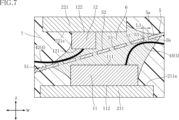
- FIG. 7 is a partially enlarged view of FIG. 6.
- FIG. FIG. 8 is a plan view similar to FIG. 3, showing an arrangement example of openings in the first sheet.
- FIG. 9 is a cross-sectional view, similar to FIG.
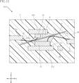
- FIG. 10 is a cross-sectional view, similar to FIG. 6, showing a semiconductor device according to a second modification of the first embodiment.
- FIG. 11 is a cross-sectional view, similar to FIG. 6, showing a semiconductor device according to a third modification of the first embodiment.
- FIG. 12 is a plan view showing a semiconductor device according to a second embodiment of the present disclosure;
- FIG. 13 is a plan view of the semiconductor device shown in FIG. 12, and is a view through the first sheet and the sealing resin.
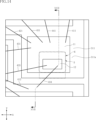
- 14 is a partially enlarged view of FIG. 13.
- FIG. 15 is a front view of the semiconductor device shown in FIG. 12.
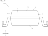
- FIG. 16 is a right side view of the semiconductor device shown in FIG. 12.
- FIG. 17 is a cross-sectional view along line XVII-XVII of FIG. 14.
- a certain entity A is formed on a certain entity B” and “a certain entity A is formed on a certain entity B” mean “a certain entity A is formed on a certain entity B”. It includes "being directly formed in entity B” and “being formed in entity B while another entity is interposed between entity A and entity B”.
- ⁇ an entity A is placed on an entity B'' and ⁇ an entity A is located on an entity B'' mean ⁇ an entity A is located on an entity B.'' It includes "directly placed on B” and "some entity A is placed on an entity B while another entity is interposed between an entity A and an entity B.”
- ⁇ an object A is located on an object B'' means ⁇ an object A is adjacent to an object B and an object A is positioned on an object B. and "the thing A is positioned on the thing B while another thing is interposed between the thing A and the thing B".
- ⁇ an object A overlaps an object B when viewed in a certain direction'' means ⁇ an object A overlaps all of an object B'' and ⁇ an object A overlaps an object B.'' It includes "overlapping a part of a certain thing B".
- FIG. 1 A semiconductor device A10 according to the first embodiment of the present disclosure will be described based on FIGS. 1 to 8.
- FIG. The semiconductor device A10 includes a light receiving element 11, a light emitting element 12, a conductive support member 2, a plurality of wires 4, a first sheet 5, a transparent resin 6 and a sealing resin 7.
- FIG. 1 is a plan view showing the semiconductor device A10.
- FIG. 2 is a plan view of the semiconductor device A10.
- the outlines of the first sheet 5 and the sealing resin 7 are shown by imaginary lines (chain lines).
- the transparent resin 6 is omitted.
- 3 is a partially enlarged view of FIG. 2.
- FIG. 4 is a front view of the semiconductor device A10.
- FIG. 5 is a right side view of the semiconductor device A10.
- 6 is a cross-sectional view taken along line VI-VI of FIG. 3.
- FIG. 7 is a partially enlarged view of FIG. 6.
- the semiconductor device A10 of this embodiment includes a plurality of (two in the illustrated example) light receiving elements 11 and a plurality of (two in the illustrated example) light emitting elements 12 .
- the semiconductor device A10 shown in these figures is a device that is surface-mounted on circuit boards of various devices.
- the application and function of the semiconductor device A10 are not limited.
- the package format of the semiconductor device A10 is SOP (Small Outline Package). Note that the package format of the semiconductor device A10 is not limited to the SOP.
- the shape of the portion of the semiconductor device A10 covered with the sealing resin 7 is rectangular when viewed in the thickness direction.
- the thickness direction of the semiconductor device A10 is called "thickness direction z”.
- a direction perpendicular to the thickness direction z is called a “direction x”.
- a direction perpendicular to both the thickness direction z and the direction x is called a "direction y.”
- Each dimension of the semiconductor device A10 is not particularly limited.
- the conductive support member 2 is a conductive member that constitutes a conductive path between each light receiving element 11 and each light emitting element 12 and the circuit board on which the semiconductor device A10 is mounted.
- the conductive support member 2 is part of a lead frame used when manufacturing the semiconductor device A10. Although the thickness of the conductive support member 2 is not particularly limited, it is, for example, about 200 ⁇ m.
- the conductive support member 2 is preferably made of either Cu or Ni, an alloy thereof, 42 alloy, or the like.
- the conductive support member 2 includes leads 21-29. Each lead 21-29 is spaced apart from each other.
- the lead 21 supports each light receiving element 11 and is electrically connected to the light receiving element 11 .
- the lead 21 has a first die pad 211 and a terminal portion 212 .
- the first die pad 211 is arranged in the center (or approximately the center) of the direction x and the direction y in the semiconductor device A10. As shown in FIGS. 2 and 3, the first die pad 211 has two light receiving elements 11 mounted thereon.
- the first die pad 211 has a long rectangular shape that is relatively long along the direction x when viewed in the thickness direction z.
- the first die pad 211 is electrically connected to each light receiving element 11 via a wire 4 (a wire 41 to be described later).
- First die pad 211 is covered with transparent resin 6 and sealing resin 7 .
- the first die pad 211 has a first major surface 211a.
- the first main surface 211a faces one side in the thickness direction z.
- the first main surface 211a is flat (or substantially flat).
- Each light receiving element 11 is bonded to the first main surface 211a. As shown in FIGS. 2 and 3, the two light receiving elements 11 are spaced apart in the direction x.
- the terminal portion 212 is connected to one side of the first die pad 211 in the y direction (the upper side in FIG. 2), extends in the one side of the y direction, and is partly exposed from the sealing resin 7. are doing.
- the terminal portion 212 is electrically connected to each light receiving element 11 via the first die pad 211 and the wire 41 .
- the portion of the terminal portion 212 exposed from the sealing resin 7 is bent like a hook when viewed in the direction x. Note that the shape of the lead 21 is not limited to the above.
- the lead 22 supports the light emitting element 12 and is electrically connected with the light emitting element 12 .
- the lead 22 has a second die pad 221 and a terminal portion 222 .
- the second die pad 221 is arranged on the semiconductor device A10 near the other side in the direction x and in the center (or approximately the center) in the direction y. As shown in FIGS. 2, 3 and 6, the second die pad 221 is spaced apart from the first die pad 211 on one side in the thickness direction z, and is the second die pad when viewed in the thickness direction z. It overlaps with 1 die pad 211 .
- the second die pad 221 has one light receiving element 11 mounted thereon.
- the second die pad 221 has a rectangular shape (or a substantially rectangular shape) when viewed in the thickness direction z. As shown in FIGS. 2, 3, 6, etc., the second die pad 221 is covered with the transparent resin 6 and the sealing resin 7. As shown in FIG.
- the second die pad 221 has a second major surface 221a.
- the second main surface 221 a faces the other side in the thickness direction z and faces the first main surface 211 a of the first die pad 211 .
- the second main surface 221a is flat (or substantially flat).
- One of the two light emitting elements 12 is bonded to the second main surface 221a.
- the terminal portion 222 is connected to the other side of the second die pad 221 in the y direction (lower side in FIG. 2) and extends in the other side of the y direction so that a part of the terminal portion 222 extends from the sealing resin 7. Exposed.
- the terminal portion 222 is electrically connected to the light emitting element 12 via the second die pad 221 .
- a portion of the terminal portion 222 exposed from the sealing resin 7 is bent like a hook when viewed in the direction x. Note that the shape of the lead 22 is not limited to the above.
- the lead 23 supports the light emitting element 12 and is electrically connected with the light emitting element 12 .
- the lead 23 has a second die pad 231 and a terminal portion 232 .
- the lead 23 has a configuration similar to that of the lead 22 .
- the second die pad 231 is arranged on the semiconductor device A10 near one side in the direction x and in the center (or approximately the center) in the direction y.
- the second die pad 231 is located on one side of the second die pad 221 in the direction x.
- the second die pad 231 is spaced apart from the first die pad 211 on one side in the thickness direction z, and overlaps the first die pad 211 when viewed in the thickness direction z. ing.
- the second die pad 231 has one light receiving element 11 mounted thereon.
- the second die pad 231 has a rectangular shape (or a substantially rectangular shape) when viewed in the thickness direction z.
- the second die pad 231 is covered with the transparent resin 6 and the sealing resin 7 similarly to the second die pad 221 .
- the second die pad 231 has a second major surface 231a.
- the second main surface 231a like the second main surface 221a, faces the other side in the thickness direction z, faces the first main surface 211a of the first die pad 211, and is flat (or substantially flat). be.
- the other of the two light emitting elements 12 is bonded to the second main surface 231a.
- the terminal portion 232 is connected to the other side of the second die pad 231 in the y direction (lower side in FIG. 2) and extends in the other side of the y direction so that a part of the terminal portion 232 extends from the sealing resin 7. Exposed.
- the terminal portion 232 is electrically connected to the light emitting element 12 via the second die pad 231 .
- a portion of the terminal portion 232 exposed from the sealing resin 7 is bent like a hook when viewed in the direction x. Note that the shape of the lead 23 is not limited to the above.
- the lead 24 is electrically connected to the light emitting element 12.
- the lead 24 has a pad portion 241 and a terminal portion 242 .
- the pad section 241 is arranged on the other side in the direction x and the other side in the direction y with respect to the second die pad 221, as shown in FIGS.
- the pad portion 241 is electrically connected to the light emitting element 12 (the light emitting element 12 mounted on the second main surface 221a of the second die pad 221) via the wire 4 (wire 42 described later).
- the pad portion 241 is covered with the sealing resin 7 .
- the pad portion 241 has a rectangular shape when viewed in the thickness direction z.
- the wire 42 is joined to the surface of the pad portion 241 facing the other side in the thickness direction z.
- the terminal portion 242 is connected to the pad portion 241, extends to the other side in the direction y (lower side in FIG. 2), and is partly exposed from the sealing resin 7. As shown in FIG. The terminal portion 242 is electrically connected to the light emitting element 12 via the pad portion 241 and the wire 42 . A portion of the terminal portion 242 exposed from the sealing resin 7 is bent like a hook when viewed in the direction x. Note that the shape of the lead 24 is not limited to the above.
- the lead 25 is electrically connected to the light emitting element 12.
- the lead 25 has a pad portion 251 and a terminal portion 252 .
- the lead 25 has a configuration similar to that of the lead 24 .
- the pad section 251 is arranged on one side in the direction x and the other side in the direction y with respect to the second die pad 231, as shown in FIGS.
- the pad portion 251 is electrically connected to the light emitting element 12 (the light emitting element 12 mounted on the second main surface 231a of the second die pad 231) through the wire 4 (wire 43 described later).
- the pad portion 251 is covered with the sealing resin 7 .
- the pad portion 251 has a rectangular shape when viewed in the thickness direction z.
- the wire 43 is joined to the surface of the pad portion 251 facing the other side in the thickness direction z.
- the terminal portion 252 is connected to the pad portion 251, extends to the other side in the direction y (lower side in FIG. 2), and is partly exposed from the sealing resin 7. As shown in FIG. The terminal portion 252 is electrically connected to the light emitting element 12 via the pad portion 251 and the wire 43 . As shown in FIG. 5, the portion of the terminal portion 252 exposed from the sealing resin 7 is bent like a hook when viewed in the direction x. Note that the shape of the lead 25 is not limited to the above.
- the terminal portions 242, 222, 232, and 252 protrude from the surface of the sealing resin 7 on the other side in the direction y (resin side surface 75, which will be described later), and extend from the other side in the direction x to one side. They are arranged in order and evenly spaced.
- the lead 26 is electrically connected to the light receiving element 11.
- the lead 26 has a pad portion 261 and a terminal portion 262 .
- the pad section 261 is arranged on the other side in the direction x and one side in the direction y with respect to the first die pad 211, as shown in FIGS.
- the pad portion 261 is electrically connected to the light receiving element 11 (the light receiving element 11 arranged on the other side in the direction x) via a wire 4 (a wire 44 to be described later).
- the pad portion 261 is covered with the sealing resin 7 .
- the pad portion 261 has a rectangular shape (or a substantially rectangular shape) when viewed in the thickness direction z.
- the wire 44 is joined to the surface of the pad portion 261 facing one side in the thickness direction z.
- the terminal portion 262 is connected to one side of the pad portion 261 in the direction y (the upper side in FIG. 2), extends in the direction y, and is partly exposed from the sealing resin 7. ing.
- the terminal portion 262 is electrically connected to the light receiving element 11 via the pad portion 261 and the wire 44 .
- a portion of the terminal portion 262 exposed from the sealing resin 7 is bent like a hook when viewed in the direction x. Note that the shape of the lead 26 is not limited to the above.
- the lead 27 is electrically connected to the light receiving element 11.
- the lead 27 has a pad portion 271 and a terminal portion 272 .
- the pad section 271 is arranged on one side of the first die pad 211 in the direction y, as shown in FIG.
- the pad portion 271 is electrically connected to the light-receiving element 11 (the light-receiving element 11 arranged on the other side in the direction x) via the wire 4 (a wire 45 described later).
- the pad portion 271 is covered with the sealing resin 7 .
- the pad portion 271 has a rectangular shape (or a substantially rectangular shape) when viewed in the thickness direction z.
- the wire 45 is joined to the surface of the pad portion 271 facing one side in the thickness direction z.
- the terminal portion 272 is connected to one side of the pad portion 271 in the y direction (the upper side in FIG. 2), extends in the one side of the y direction, and is partly exposed from the sealing resin 7 . ing.
- the terminal portion 272 is electrically connected to the light receiving element 11 via the pad portion 271 and the wire 45 .
- a portion of the terminal portion 272 exposed from the sealing resin 7 is bent like a hook when viewed in the direction x. Note that the shape of the lead 27 is not limited to the above.
- the lead 28 is electrically connected to the light receiving element 11.
- the lead 28 has a pad portion 281 and a terminal portion 282 .
- the lead 28 has a configuration similar to that of the lead 27 .
- the pad section 281 is arranged on one side of the first die pad 211 in the direction y, as shown in FIG.
- the pad portion 281 is electrically connected to the light receiving element 11 (the light receiving element 11 arranged on one side in the direction x) via a wire 4 (a wire 46 to be described later).
- the pad portion 281 is covered with the sealing resin 7 .
- the pad portion 281 has a rectangular shape (or a substantially rectangular shape) when viewed in the thickness direction z.
- the wire 46 is joined to the surface of the pad portion 281 facing one side in the thickness direction z.
- the terminal portion 282 is connected to one side of the pad portion 281 in the y direction (the upper side in FIG. 2) and extends in the one side of the y direction so that a portion of the terminal portion 282 is exposed from the sealing resin 7 . ing.
- the terminal portion 282 is electrically connected to the light receiving element 11 via the pad portion 281 and the wire 46 .
- a portion of the terminal portion 282 exposed from the sealing resin 7 is bent like a hook when viewed in the direction x. Note that the shape of the lead 28 is not limited to the above.
- the terminal portions 262, 272, 282, and 212 protrude from one surface of the sealing resin 7 in the direction y (resin side surface 76, which will be described later), and extend from the other side in the direction x to one side. They are arranged in order and evenly spaced.
- the lead 29 is arranged on one side of the first die pad 211 in the direction y, as shown in FIGS.
- the lead 29 has a long rectangular shape that is relatively long along the direction x when viewed in the thickness direction z.
- the leads 29 are covered with the sealing resin 7 .
- a wire 4 (a wire 47 and a wire 48, which will be described later) is joined to a surface of the lead 29 facing one side in the thickness direction z.
- the light emitting element 12 is, for example, an LED chip, and is configured to emit light of a certain wavelength.
- a constituent material of the light emitting element 12 includes a semiconductor material.
- the light emitting element 12 has a rectangular plate shape when viewed in the thickness direction z.
- the light emitting element 12 has a main surface 121 and a back surface 122, as shown in FIG.
- the main surface 121 and the back surface 122 face opposite sides in the thickness direction z.
- the main surface 121 faces the other side in the thickness direction z.
- the back surface 122 faces one side in the thickness direction z.
- the light emitting element 12 includes a cathode electrode (not shown) arranged on the main surface 121 and an anode electrode (not shown) arranged on the back surface 122 .
- the light emitting element 12 on one side and the light emitting element 12 on the other side shown in FIG. 7 are bonded to the second main surfaces 221a, 231a of the second die pads 221, 231 via a bonding material (not shown).
- the bonding material is a conductive bonding material, and is not particularly limited, but is, for example, solder.
- the back surface 122 of the light emitting element 12 is bonded to the second main surface 221a (231a) of the second die pad 221 (231) with a bonding material.
- the anode electrode of the light emitting element 12 is conductively connected to the second die pad 221 (231) via a bonding material.
- the terminal portions 222 and 232 of the leads 22 and 23 are electrically connected to the anode electrode of the light emitting element 12 and function as anode terminals.
- the cathode electrode of the light emitting element 12 is conductively connected to the pad portion 241 (251) of the lead 24 (25) through the wire 42 (43).
- the terminal portions 242 and 252 of the leads 24 and 25 are electrically connected to the cathode electrode of the light emitting element 12 and function as cathode terminals.
- a part of the light emitting element 12 including at least the main surface 121 is covered with the transparent resin 6 .
- the light emitting element 12 emits light according to the current that flows when a voltage is applied between the anode electrode and the cathode electrode. Light emitted by the light emitting element 12 travels through the transparent resin 6 and reaches the light receiving element 11 .
- the light receiving element 11 receives light emitted by the light emitting element 12 .
- a constituent material of the light receiving element 11 includes a semiconductor material.
- the light receiving element 11 has a rectangular plate shape when viewed in the thickness direction z.
- the light receiving element 11 has a main surface 111 and a back surface 112, as shown in FIG.
- the principal surface 111 and the back surface 112 face opposite sides in the thickness direction z.
- the main surface 111 faces one side in the thickness direction z.
- Main surface 111 faces main surface 121 of light emitting element 12 .
- the back surface 112 faces the other side in the thickness direction z.
- the one light-receiving element 11 and the other light-receiving element 11 shown in FIG. 7 are bonded to the first main surface 211a of the first die pad 211 via a bonding material (not shown).
- the bonding material is not particularly limited, but is, for example, an insulating bonding material.
- the back surface 112 of the light receiving element 11 is bonded to the first main surface 211a of the first die pad 211 with a bonding material.
- a light receiving portion and a circuit forming portion are arranged on the main surface 111 of the light receiving element 11 .
- the light-receiving part is arranged on the other side of the main surface 111 in the direction y.
- the light receiving section has, for example, a photodiode and generates an electromotive force according to the amount of received light.
- a main surface 111 of the light receiving element 11 is entirely covered with a transparent resin 6 . As a result, the light receiving section can appropriately receive the light from the light emitting element 12 through the transparent resin 6 .
- the circuit forming portion is arranged on one side of the main surface 111 in the direction y.
- a circuit including a transistor or the like is formed in the circuit forming portion.
- the circuit forming portion amplifies and outputs an electromotive force generated by the light receiving portion upon receiving the light.
- a plurality of electrodes are arranged in the circuit forming portion. Each electrode is conductively connected to leads 21, 26, 27 (21, 26, 28) via wires 4, as shown in FIG.
- the power electrode of the light receiving element 11 is conductively connected to the pad portion 261 of the lead 26 via the wire 44 (47, 48).
- the terminal portion 262 of the lead 26 is electrically connected to the power supply electrode of the light receiving element 11 and functions as a power supply terminal.
- a ground electrode of the light receiving element 11 is conductively connected to the first die pad 211 via the wire 41 .
- the terminal portion 212 of the lead 21 is electrically connected to the ground electrode of the light receiving element 11 and functions as a ground terminal.
- the output electrode of the light receiving element 11 is conductively connected to the pad portion 271 (281) of the lead 27 (28) via the wire 45 (46).
- the terminal portion 272 (282) of the lead 27 (28) is electrically connected to the output electrode of the light receiving element 11 and functions as an output terminal.
- the semiconductor device A10 When a voltage is applied between the terminal portion 222 (232) and the terminal portion 242 (252), the voltage is applied between the anode electrode and the cathode electrode of the light emitting element 12, current flows, and the light emitting element 12 is turned on. luminous.
- the light receiving portion of the light receiving element 11 When the light receiving portion of the light receiving element 11 receives light, it generates an electromotive force corresponding to the amount of received light.
- the electromotive force is amplified by a power source supplied between the terminal portion 262 and the terminal portion 212 in the circuit forming portion and output from the terminal portion 272 (282).
- the semiconductor device A10 is configured such that the input side (terminals 222, 232 and terminal sections 242, 252) and the output side (terminals 272, 282) are electrically insulated from each other. can transmit a signal to
- the plurality of wires 4 are conductive members that together with the conductive support member 2 constitute conductive paths between the light emitting element 12 and the light receiving element 11 and the circuit board.
- a constituent material of each of the plurality of wires 4 is a metal containing Au, Cu, or Al, for example.
- the plurality of wires 4 includes wires 41-48.
- the wire 41 constitutes a conductive path between the light receiving element 11 and the lead 21.
- the wire 41 is joined to the ground electrode of the light receiving element 11 and the first die pad 211 .
- the wire 42 is joined to the cathode electrode of one light emitting element 12 and the pad portion 241 of the lead 24 .
- the wire 43 is joined to the cathode electrode of the other light emitting element 12 and the pad portion 251 of the lead 25 .
- a wire 44 constitutes a conductive path between one light receiving element 11 and the lead 26 .
- the wire 44 is joined to the power supply electrode of the light receiving element 11 and the pad portion 261 of the lead 26 .
- a wire 45 constitutes a conductive path between one light receiving element 11 and the lead 27 .
- the wire 45 is joined to the output electrode of the light receiving element 11 and the pad portion 271 of the lead 27 .
- the number of wires 45 is not limited.
- a wire 46 constitutes a conductive path between the other light receiving element 11 and the lead 28 .
- the wire 46 is joined to the output electrode of the light receiving element 11 and the pad portion 281 of the lead 28 .
- a wire 47 constitutes a conducting path between the lead 29 and the lead 26 .
- Wire 47 is joined to lead 29 and pad portion 261 of lead 26 . Note that the number of wires 47 is not limited. Note that the number of wires 47 is not limited. A wire 48 constitutes a conductive path between the other light receiving element 11 and the lead 26 . A wire 48 is joined to the power supply electrode of the light receiving element 11 and the lead 29 . Note that the number of wires 48 is not limited.
- the first sheet 5 is interposed between the light receiving element 11 and the light emitting element 12 in the thickness direction z, as shown in FIG. 6 and the like.
- the first sheet 5 is a plate-shaped member having translucency and insulation.
- the constituent material of the first sheet 5 is not particularly limited as long as it is an insulating material through which light can pass, and for example, the entire first sheet 5 is made of a transparent material.
- the first sheet 5 has a rectangular shape when viewed in the thickness direction z.
- the first sheet 5 overlaps all of the light receiving element 11, the light emitting element 12, the first die pad 211, and the second die pads 221 and 231 when viewed in the thickness direction z.
- the light emitted by the light-emitting element 12 can pass through the first sheet 5 between the light-receiving element 11 facing the light-emitting element 12 .
- seat 5 is not limited above.
- the first sheet 5 has a first surface 5a and a second surface 5b.
- the first surface 5a faces one side in the thickness direction z.
- the second surface 5b faces the side opposite to the first surface 5a and faces the other side in the thickness direction z.
- the first sheet 5 has a thickness direction from the other side of the direction y (left side in the figure) toward the one side of the direction y (right side in the figure) when viewed in the direction x. It is inclined so as to be located on one side of z (upper side in the figure).
- the first sheet 5 has uneven portions 51 , flat portions 52 and a plurality of openings 53 .
- the uneven portion 51 is a portion in which at least a part of the surfaces of the first surface 5a and the second surface 5b is formed in an uneven shape.
- the shape and arrangement of the uneven portion 51 and the height of the unevenness are not limited.
- the uneven portion 51 is provided in a region of the first sheet 5 near the outer periphery. More specifically, the uneven portion 51 is provided on both the first surface 5a and the second surface 5b in the annular region near the outer periphery of the first sheet 5 . It is preferable that the uneven portion 51 have a surface roughness equal to or greater than a predetermined value.
- Concavo-convex portion 51 has a surface area that is 1.5 times or more the surface area when no concavo-convex portion is formed, for example.
- the upper limit of the surface area of the uneven portion 51 is not particularly limited. As an example, in order to prevent problems such as the thickness of the first sheet 5 from becoming extremely uneven, the surface area of the uneven portion 51 is 2.5 times or less of the surface area when the unevenness is not formed. Preferably.
- the flat portion 52 is a portion that is flatter than the uneven portion 51 .
- the flat portion 52 is provided in an inner region surrounded by the uneven portion 51 .
- Each of the plurality of openings 53 is a through hole penetrating from the first surface 5a to the second surface 5b.
- the shape and arrangement of the opening 53 are not particularly limited.
- FIG. 8 is a plan view showing an example of arrangement of the plurality of openings 53. As shown in FIG. The illustrated example represents a case where the shape of each of the plurality of openings 53 is circular.
- the plurality of openings 53 are distributed in the in-plane direction of the first sheet 5 .
- the multiple openings 53 are provided in the flat portion 52 .
- the size of each opening 53 is not limited. To give an example of the size of each opening 53, as shown in FIG. The range is double to double. In this embodiment, since the opening 53 is circular, the diameter of the opening 53 is about 0.5 to 2 times the diameter of the wire 4, for example.
- the transparent resin 6 covers part of the conductive support member 2, part of the light receiving element 11 (at least the main surface 111), and part of the light emitting element 12 (at least the main surface 111). 121 ), part of the wire 4 and part of the first sheet 5 .
- the transparent resin 6 has electrical insulation.
- the transparent resin 6 contains transparent epoxy resin, for example.
- the constituent material of the transparent resin 6 is not limited as long as it is a material having translucency.
- the transparent resin 6 is, for example, between the light receiving element 11 and the first sheet 5 (second surface 5b) and between the light emitting element 12 and the first sheet 5 (first surface 5a). Formed by potting.
- the formation method of the transparent resin 6 is not limited to the above.
- the transparent resin 6 is in contact only with the flat portion 52 (the first surface 5 a and the second surface 5 b of the flat portion 52 ) of the first sheet 5 and covers most of the flat portion 52 .
- the transparent resin 6 is filled in each opening 53 of the first sheet 5 .
- the transparent resin 6 described above is an example of the "resin portion" of the present disclosure.
- the sealing resin 7 covers part of the conductive support member 2 , the light receiving element 11 , the light emitting element 12 , part of the wire 4 , part of the first sheet 5 , and the transparent resin 6 . More specifically, the sealing resin 7 is in contact with the entire uneven portion 51 and part of the flat portion 52 of the first sheet 5 .
- the sealing resin 7 has electrical insulation. Sealing resin 7 contains, for example, black epoxy resin. In addition, the constituent material of the sealing resin 7 is not limited.
- the sealing resin 7 is formed, for example, by transfer molding using a mold.
- the sealing resin 7 has a rectangular shape when viewed in the thickness direction z.
- the sealing resin 7 has a resin top surface 71, a resin bottom surface 72, and resin side surfaces 73-76.
- the resin top surface 71 and the resin bottom surface 72 face opposite sides in the thickness direction z.
- the resin top surface 71 faces one side in the thickness direction z, and the resin bottom surface 72 faces the other side in the thickness direction z.
- the resin top surface 71 and the resin bottom surface 72 are flat (or substantially flat).
- Each of the resin side surfaces 73 to 76 is connected to the resin top surface 71 and the resin bottom surface 72, and is sandwiched between the resin top surface 71 and the resin bottom surface 72 in the thickness direction z.
- the resin side surface 73 and the resin side surface 74 face opposite sides in the direction x.
- the resin side surface 73 faces the other side in the direction x, and the resin side surface 74 faces one side in the direction x.
- the resin side surface 75 and the resin side surface 76 face opposite to each other in the direction y.
- the resin side surface 75 faces the other side in the direction y, and the resin side surface 76 faces the one side in the direction y. As shown in FIG.
- each of the terminal portions 242 , 222 , 232 , 252 protrudes from the resin side surface 75 .
- a part of each of the terminal portions 262 , 272 , 282 , 212 protrudes from the resin side surface 76 .
- the conductive support member 2 is not exposed from the resin side surface 73 and the resin side surface 74 .
- the resin side surfaces 73 to 76 each have surfaces connected to the resin top surface 71 and inclined so as to approach each other toward the resin top surface 71 . That is, the portion of the sealing resin 7 connected to the resin top surface 71 and surrounded by the inclined surfaces has a tapered shape in which the cross-sectional area in the xy plane becomes smaller toward the resin top surface 71 . Further, the resin side surfaces 73 to 76 each have surfaces connected to the resin bottom surface 72 and inclined so as to approach each other toward the resin bottom surface 72 .
- the portion of the sealing resin 7 connected to the resin bottom surface 72 and surrounded by the inclined surfaces has a tapered shape in which the cross-sectional area in the xy plane becomes smaller toward the resin bottom surface 72 .
- the shape of the sealing resin 7 shown in FIGS. 1, 4, and 5 is an example.
- the shape of the sealing resin 7 is not limited to the illustrated shape.
- the sealing resin 7 described above is an example of the "resin portion" of the present disclosure.
- the semiconductor device A10 includes a light receiving element 11, a light emitting element 12, a first sheet 5, a transparent resin 6 and a sealing resin 7.
- the light receiving element 11 is mounted on the first main surface 211a of the first die pad 211 facing one side in the thickness direction z.
- the light emitting element 12 is arranged on one side of the light receiving element 11 in the thickness direction z.
- the first sheet 5 has a first surface 5a and a second surface 5b facing one side and the other side in the thickness direction z.
- the first sheet 5 has translucency and insulation, and is interposed between the light receiving element 11 and the light emitting element 12 in the thickness direction z.
- the first sheet 5 is covered with transparent resin 6 and sealing resin 7 . At least a part of the first surface 5a and the second surface 5b of the first sheet 5 includes an uneven portion 51 in which unevenness is formed.
- the uneven portions 51 of the first sheet 5 that are in contact with the transparent resin 6 or the sealing resin 7 have improved adhesion with the transparent resin 6 or the sealing resin 7 .
- the first sheet 5 is prevented from peeling off from the covering transparent resin 6 or the sealing resin 7, and a decrease in dielectric strength voltage can be suppressed.
- the light emitting element 12 is mounted on a second die pad 221 (231) spaced apart from the first die pad 211 on one side in the thickness direction z.
- the light emitting element 12 is mounted on the second main surface 221a (231a) of the second die pad 221 (231) facing the other side in the thickness direction z.
- the light emitting element 12 overlaps the light receiving element 11 when viewed in the thickness direction z.
- the first sheet 5 is arranged between the light receiving element 11 and the light emitting element 12 facing each other in the thickness direction z.
- the transparent resin 6 partially covers the light receiving element 11 and the light emitting element 12 and partially covers the first sheet 5 .
- the sealing resin 7 covers the transparent resin 6 and part of the first sheet 5 .
- the uneven portion 51 of the first sheet 5 is provided in a region near the outer periphery of the first sheet 5 and is in contact with the sealing resin 7 . According to such a configuration, the first sheet 5 disposed between the light receiving element 11 and the light emitting element 12 facing each other can be peeled off from the sealing resin 7 when the uneven portion 51 comes into contact with the sealing resin 7 . is appropriately prevented, and a decrease in dielectric strength voltage can be suppressed.
- the first surface 5 a and the second surface 5 b of the first sheet 5 include flat portions 52 that are flatter than the uneven portions 51 .
- the transparent resin 6 is in contact only with the flat portion 52 (the first surface 5a and the second surface 5b in the flat portion 52 which is the inner region of the uneven portion 51).
- a plurality of openings 53 are formed in the first sheet 5 .
- Each opening 53 penetrates from the first surface 5a to the second surface 5b.
- Each opening 53 is provided in the flat portion 52, and each opening 53 is filled with the transparent resin 6 (resin portion).
- the adhesion between the portion of the first sheet 5 where the openings 53 are formed and the transparent resin 6 (resin portion) is improved. This prevents the portion of the first sheet 5 where the opening 53 is formed from peeling off from the transparent resin 6, thereby further suppressing a decrease in dielectric strength voltage.
- a wire 4 is joined to the light receiving element 11 and the light emitting element 12 .
- the dimension L1 in the direction w of the wire 4 extending in the thickness direction z of each opening 53 is in the range of 0.5 to 2 times the diameter of the wire 4 . According to such a configuration, the wire 4 joined to the light receiving element 11 and the wire 4 joined to the light emitting element 12 do not come into contact through the opening 53, and the light receiving element 11 side and the light emitting element 12 side do not contact each other. Dielectric strength is properly maintained.
- FIG. 9 shows a semiconductor device according to a first modification of the first embodiment.
- FIG. 9 is a cross-sectional view similar to FIG. 6 shown in the above embodiment.
- elements that are the same as or similar to those of the semiconductor device A10 of the above embodiment are assigned the same reference numerals as those of the above embodiment, and description thereof will be omitted as appropriate.
- the configuration of the first sheet 5 is different from that of the above embodiment.
- the opening 53 is not formed in the first sheet 5 .
- the first sheet 5 is covered with transparent resin 6 and sealing resin 7 .
- At least a part of the first surface 5a and the second surface 5b of the first sheet 5 includes an uneven portion 51 in which unevenness is formed.
- the uneven portions 51 of the first sheet 5 that are in contact with the transparent resin 6 or the sealing resin 7 have improved adhesion with the transparent resin 6 or the sealing resin 7 .
- the first sheet 5 is prevented from peeling off from the covering transparent resin 6 or the sealing resin 7, and a decrease in dielectric strength voltage can be suppressed.
- the same effects as those of the above embodiment can be obtained.
- FIG. 10 shows a semiconductor device according to a second modification of the first embodiment.
- FIG. 10 is a cross-sectional view similar to FIG. 6 shown in the above embodiment.
- the configuration of the first sheet 5 is different from that of the above embodiment.
- the uneven portion 51 is not provided on the first sheet 5 .
- the first sheet 5 is covered with transparent resin 6 and sealing resin 7 .
- Each opening 53 of the first sheet 5 is filled with the transparent resin 6 .
- the adhesion between the portion of the first sheet 5 where each opening 53 is formed and the transparent resin 6 (resin portion) is improved. This prevents the portion of the first sheet 5 where the opening 53 is formed from peeling off from the transparent resin 6, thereby suppressing a decrease in dielectric strength voltage.
- the same effects as those of the above embodiment can be obtained.
- FIG. 11 shows a semiconductor device according to a third modification of the first embodiment.
- FIG. 11 is a cross-sectional view similar to FIG. 6 shown in the above embodiment.
- the configuration of the first sheet 5 is different from that of the above embodiment.
- the uneven portion 51 is provided over the entire first sheet 5, and the opening 53 is not formed. More specifically, the entire surfaces of the first surface 5a and the second surface 5b are uneven portions 51 formed with unevenness.
- the first sheet 5 is covered with transparent resin 6 and sealing resin 7 .
- the uneven portions 51 of the first sheet 5 that are in contact with the transparent resin 6 or the sealing resin 7 have improved adhesion with the transparent resin 6 or the sealing resin 7 .
- the first sheet 5 is prevented from peeling off from the covering transparent resin 6 or the sealing resin 7, and a decrease in dielectric strength voltage can be suppressed.
- the entire surfaces of the first surface 5a and the second surface 5b are formed as uneven portions 51. As shown in FIG. This further improves the adhesion between the first sheet 5 and the transparent resin 6 or the sealing resin 7 . This is more preferable for suppressing a decrease in dielectric strength voltage.
- the same effects as those of the above embodiment can be obtained.
- the uneven portions 51 of the first sheet 5 are provided on both the first surface 5a and the second surface 5b. Only one of the first surface 5a and the second surface 5b may be provided.
- the semiconductor devices A10, A11, A12, and A13 are configuration examples in which two light-receiving elements 11 and two light-emitting elements 12 are provided. may In this case, some of the leads 21 to 28 forming the conductive support member 2 are used as so-called dummy terminals and are not electrically connected to either the light receiving element 11 or the light emitting element 12.
- FIG. A semiconductor device A20 according to the second embodiment of the present disclosure will be described based on FIGS. 12 to 17.
- FIG. A semiconductor device A20 of this embodiment includes a light receiving element 11, a light emitting element 12, a conductive support member 3, a plurality of wires 4, a first sheet 5, a transparent resin 6 and a sealing resin 7.
- FIG. In this embodiment, the arrangement of the light receiving element 11 and the light emitting element 12 is significantly different from that of the above embodiment. Accordingly, a conductive support member 3 is provided instead of the conductive support member 2 of the above embodiment.
- FIG. 12 is a plan view showing the semiconductor device A20.
- FIG. 13 is a plan view of the semiconductor device A20. In FIG. 13, for convenience of understanding, the outlines of the first sheet 5 and the sealing resin 7 are shown by imaginary lines (chain lines). 14 is a partially enlarged view of FIG. 13.
- FIG. 15 is a front view of the semiconductor device A20.
- FIG. 16 is a right side view of the semiconductor device A20.
- 17 is a cross-sectional view along line XVII-XVII of FIG. 14.
- the first sheet 5 and the light emitting element 12 are stacked on one side of the light receiving element 11 in the thickness direction z.
- the semiconductor device A20 of this embodiment includes two light receiving elements 11 and two light emitting elements 12, as shown in FIG. One first sheet 5 is arranged between each pair of light receiving element 11 and light emitting element 12 in the thickness direction z.
- the first sheet 5 is interposed between the main surface 111 of the light receiving element 11 and the back surface 122 of the light emitting element 12 in the thickness direction z.
- the first sheet 5 includes a first area 501 , a second area 502 and a third area 503 .
- the first region 501 is a portion overlapping both the light receiving element 11 and the light emitting element 12 when viewed in the thickness direction z.
- the second region 502 is a portion that overlaps the light receiving element 11 and does not overlap the light emitting element 12 when viewed in the thickness direction z.
- the third region 503 is a portion that overlaps neither the light receiving element 11 nor the light emitting element 12 when viewed in the thickness direction z.
- a transparent resin 6 is interposed between the light receiving element 11 and the first sheet 5 .
- the conductive support member 3 is a conductive member that constitutes a conductive path between each light receiving element 11 and each light emitting element 12 and the circuit board on which the semiconductor device A20 is mounted.
- the conductive support member 3 includes leads 31-38. Each lead 31-38 is spaced apart from each other.
- the lead 31 supports the light receiving element 11 and is electrically connected with the light receiving element 11 .
- the lead 31 has a first die pad 311 and a terminal portion 312 .
- the first die pad 311 is arranged near one side in the direction x in the semiconductor device A20 and in the center (or approximately the center) in the direction y.
- the first die pad 311 has one of the two light receiving elements 11 mounted thereon.
- the first die pad 311 has a rectangular shape (or a substantially rectangular shape) when viewed in the thickness direction z.
- the first die pad 311 is electrically connected to the light receiving element 11 via a wire 4 (a wire 411 to be described later).
- the first die pad 311 is covered with the sealing resin 7 .
- the first die pad 311 has a first major surface 311a.
- the first main surface 311a faces one side in the thickness direction z.
- the first main surface 311a is substantially flat.
- One of the two light receiving elements 11 is bonded to the first main surface 311a.
- the terminal portion 312 is connected to one side of the first die pad 311 in the y direction (upper side in FIG. 13 ), extends in the one side of the y direction, and is partly exposed from the sealing resin 7 . are doing.
- the terminal portion 312 is electrically connected to the light receiving element 11 via the first die pad 311 and the wire 411 .
- the portion of the terminal portion 312 exposed from the sealing resin 7 is bent like a hook when viewed in the direction x. Note that the shape of the lead 31 is not limited to the above.
- the lead 32 supports the light receiving element 11 and is electrically connected with the light receiving element 11 .
- the lead 32 has a first die pad 321 and a terminal portion 322 .
- the first die pad 321 is arranged on the semiconductor device A20 near the other side in the direction x and in the center (or approximately the center) in the direction y.
- the first die pad 321 mounts the other of the two light receiving elements 11 .
- the first die pad 321 has a rectangular shape (or a substantially rectangular shape) when viewed in the thickness direction z.
- the first die pad 321 is electrically connected to the light receiving element 11 via a wire 4 (a wire 412 to be described later).
- the first die pad 321 is covered with the sealing resin 7 .
- the first die pad 321 has a first major surface 321a.
- the first main surface 321a faces one side in the thickness direction z.
- the first major surface 321a is flat (or substantially flat).
- the other of the two light receiving elements 11 is bonded to the first main surface 321a.
- the terminal portion 322 is connected to the other side of the first die pad 321 in the y direction (lower side in FIG. 13), extends in the one side of the y direction, and partially extends from the sealing resin 7. Exposed.
- the terminal portion 322 is electrically connected to the light receiving element 11 via the first die pad 321 and the wire 412 .
- the portion of the terminal portion 322 exposed from the sealing resin 7 is bent like a hook when viewed in the direction x. Note that the shape of the lead 32 is not limited to the above.
- the lead 33 is electrically connected to the light receiving element 11 .
- the lead 33 has a pad portion 331 and a terminal portion 332 .
- the pad portion 331 is arranged on the other side in the direction x and one side in the direction y in the semiconductor device A20.
- the pad portion 331 is electrically connected to the light receiving element 11 (the light receiving element 11 mounted on the first die pad 311) via a wire 4 (a wire 421 to be described later).
- the pad portion 331 is covered with the sealing resin 7 .
- the pad portion 331 has a rectangular shape (or a substantially rectangular shape) when viewed in the thickness direction z.
- a wire 421 is joined to the pad portion 331 .
- the terminal portion 332 is connected to one side of the pad portion 331 in the y direction (the upper side in FIG. 13), extends in the one side of the y direction, and is partly exposed from the sealing resin 7 . ing.
- the terminal portion 332 is electrically connected to the light receiving element 11 via the pad portion 331 and the wire 421 .
- a portion of the terminal portion 332 exposed from the sealing resin 7 is bent like a hook when viewed in the direction x. Note that the shape of the lead 33 is not limited to the above.
- the lead 34 is electrically connected to the light receiving element 11 .
- the lead 34 has a pad portion 341 and a terminal portion 342 .
- the pad section 341 is arranged on one side of the first die pad 311 in the direction y.
- the pad portion 341 is electrically connected to the light receiving element 11 (the light receiving element 11 mounted on the first die pad 311) through a wire 4 (a wire 441 to be described later).
- the pad portion 341 is covered with the sealing resin 7 .
- the pad portion 341 has a rectangular shape (or a substantially rectangular shape) when viewed in the thickness direction z.
- a wire 441 is joined to the pad portion 341 .
- the terminal portion 342 is connected to one side of the pad portion 341 in the y direction, extends in one side of the y direction, and is partly exposed from the sealing resin 7 .
- Terminal portion 342 is electrically connected to light receiving element 11 via pad portion 341 and wire 441 .
- a portion of the terminal portion 342 exposed from the sealing resin 7 is bent like a hook when viewed in the direction x. Note that the shape of the lead 34 is not limited to the above.
- the lead 35 is electrically connected to the light receiving element 11.
- the lead 35 has a pad portion 351 and a terminal portion 352 .
- the pad section 351 is arranged between the pad section 331 and the pad section 341 in the direction x.
- the pad portion 351 is electrically connected to the light receiving element 11 (the light receiving element 11 mounted on the first die pad 311) via a wire 4 (a wire 451 to be described later).
- the pad portion 351 is covered with the sealing resin 7 .
- the pad portion 351 has a rectangular shape (or a substantially rectangular shape) when viewed in the thickness direction z.
- a wire 451 is joined to the pad portion 351 .
- the terminal portion 352 is connected to one side of the pad portion 351 in the y direction, extends in one side of the y direction, and is partly exposed from the sealing resin 7 .
- Terminal portion 352 is electrically connected to light receiving element 11 via pad portion 351 and wire 451 .
- a portion of the terminal portion 352 exposed from the sealing resin 7 is bent like a hook when viewed in the direction x. Note that the shape of the lead 35 is not limited to the above.
- the terminal portions 332, 352, 342, and 312 protrude from the resin side surface 76 on one side of the sealing resin 7 in the direction y, and are spaced apart from the other side in the direction x in this order. placed side by side.
- the lead 36 is electrically connected to the light receiving element 11 .
- the lead 36 has a pad portion 361 and a terminal portion 362 .
- the pad portion 361 is arranged on the other side in the direction x and the other side in the direction y in the semiconductor device A20.
- the pad portion 331 is electrically connected to the light receiving element 11 (the light receiving element 11 mounted on the first die pad 321) via a wire 4 (a wire 422 to be described later).
- the pad portion 361 is covered with the sealing resin 7 .
- the pad portion 361 has a rectangular shape (or a substantially rectangular shape) when viewed in the thickness direction z.
- a wire 422 is joined to the pad portion 361 .
- the terminal portion 362 is connected to the other side of the pad portion 361 in the y direction (lower side in FIG. 13), extends in the other direction y, and is partly exposed from the sealing resin 7. are doing.
- the terminal portion 362 is electrically connected to the light receiving element 11 via the pad portion 361 and the wire 422 .
- a portion of the terminal portion 362 exposed from the sealing resin 7 is bent like a hook when viewed in the direction x. Note that the shape of the lead 36 is not limited to the above.
- the lead 37 is electrically connected to the light receiving element 11.
- the lead 37 has a pad portion 371 and a terminal portion 372 .
- the pad section 371 is arranged on one side of the pad section 361 in the direction x.
- the pad portion 371 is electrically connected to the light receiving element 11 (the light receiving element 11 mounted on the first die pad 321) via a wire 4 (a wire 442 to be described later).
- the pad portion 371 is covered with the sealing resin 7 .
- the pad portion 371 has a rectangular shape (or a substantially rectangular shape) when viewed in the thickness direction z.
- a wire 442 is joined to the pad portion 371 .
- the terminal portion 372 is connected to the other side of the pad portion 371 in the y direction, extends in the other side of the y direction, and is partly exposed from the sealing resin 7 .
- the terminal portion 372 is electrically connected to the light receiving element 11 via the pad portion 371 and the wire 442 .
- a portion of the terminal portion 372 exposed from the sealing resin 7 is bent like a hook when viewed in the direction x. Note that the shape of the lead 37 is not limited to the above.
- the lead 38 is electrically connected to the light receiving element 11.
- the lead 38 has a pad portion 381 and a terminal portion 382 .
- the pad portion 381 is arranged on one side of the direction x with respect to the pad portion 371 .
- the pad portion 381 is electrically connected to the light receiving element 11 (the light receiving element 11 mounted on the first die pad 321) via a wire 4 (a wire 452 to be described later).
- the pad portion 381 is covered with the sealing resin 7 .
- the pad portion 381 has a rectangular shape (or a substantially rectangular shape) when viewed in the thickness direction z.
- a wire 452 is joined to the pad portion 381 .
- the terminal portion 382 is connected to the other side of the pad portion 381 in the y direction, extends in the other side of the y direction, and is partly exposed from the sealing resin 7 .
- the terminal portion 382 is electrically connected to the light receiving element 11 via the pad portion 381 and the wire 452 .
- a portion of the terminal portion 382 exposed from the sealing resin 7 is bent like a hook when viewed in the direction x. Note that the shape of the lead 38 is not limited to the above.
- the terminal portions 362, 372, 382, and 322 protrude from the resin side surface 75 on the other side in the direction y of the sealing resin 7, and are spaced in this order from the other side in the direction x to one side. placed side by side.
- the light emitting element 12 has a rectangular shape when viewed in the thickness direction z.
- the light-emitting element 12 has a main surface 121 and a back surface 122, as shown in FIG.
- the main surface 121 faces one side in the thickness direction z.
- the back surface 122 faces the other side in the thickness direction z.
- the light emitting element 12 has a cathode electrode and an anode electrode (both not shown) disposed on the main surface 121 .
- the one light emitting element 12 shown in FIG. 17 and the other light emitting element 12 are joined to the first surface 5a of the first sheet 5 via a joining material (not shown).
- the bonding material is not particularly limited, but is, for example, a bonding material having translucency and insulating properties.
- the back surface 122 of the light emitting element 12 is bonded to the first surface 5a of the first sheet 5 with a bonding material.
- the anode electrode of one light emitting element 12 (on the right side in FIG. 13) is electrically connected to the terminal portion 382 via the wire 4 (wires 433 and 452 to be described later).
- the cathode electrode of one light emitting element 12 is electrically connected to the terminal portion 322 via a wire 4 (a wire 434 to be described later).
- the anode electrode of the other light emitting element 12 (left side in FIG. 13) is electrically connected to the terminal portion 352 via the wire 4 (wires 431 and 451 to be described later).
- the cathode electrode of the other light emitting element 12 is electrically connected to the terminal portion 312 via a wire 4 (a wire 432 to be described later).
- the back surface 122 of the light emitting element 12 is covered with the first sheet 5 . Portions other than the back surface 122 of the light emitting element 12 are covered with the sealing resin 7 .
- the light emitting element 12 emits light according to the current that flows when a voltage is applied between the anode electrode and the cathode electrode. Light emitted by the light emitting element 12 mainly travels from the back surface 122 to the first sheet 5 and reaches the light receiving element 11 via the transparent resin 6 .
- the light receiving element 11 receives light emitted by the light emitting element 12 stacked thereon.
- One light receiving element 11 and the other light receiving element 11 shown in FIG. 17 are bonded to the first main surfaces 311a and 321a of the first die pads 311 and 321 via a bonding material (not shown).
- the bonding material is not particularly limited, but is, for example, an insulating bonding material.
- the back surface 112 of the light receiving element 11 is bonded to the first main surface 311a (321a) of the first die pad 311 (321) with a bonding material.
- a light receiving portion and a circuit forming portion are arranged on the main surface 111 of the light receiving element 11 .
- the light receiving portion is arranged at a position overlapping the light emitting element 12 in the thickness direction z.
- the light receiving section has, for example, a photodiode and generates an electromotive force according to the amount of received light.
- the transparent resin 6, the first sheet 5, and the light emitting element 12 are laminated in this order in the thickness direction z. Thereby, the light receiving section can appropriately receive the light from the light emitting element 12 via the first sheet 5 and the transparent resin 6 .
- the circuit forming part amplifies and outputs the electromotive force generated by the light receiving part receiving the light.
- a plurality of electrodes are arranged in the circuit forming portion. Each electrode is conductively connected to leads 31, 33, 34, 35 (32, 36, 37, 38) via wires 4, as shown in FIG.
- the power electrode of the light receiving element 11 is conductively connected to the pad portion 331 (361) of the lead 33 (36) via the wire 421 (422).
- the terminal portion 332 (362) of the lead 33 (36) is electrically connected to the power supply electrode of the light receiving element 11 and functions as a power supply terminal.
- the ground electrode of the light receiving element 11 is conductively connected to the terminal portion 312 (322) of the lead 31 (32) via the wire 411 (412).
- the terminal portion 312 (322) of the lead 31 (32) is electrically connected to the ground electrode of the light receiving element 11 and functions as a ground terminal.
- the output electrode of the light receiving element 11 is conductively connected to the pad portion 341 (371) of the lead 34 (37) via the wire 441 (442).
- the terminal portion 342 (372) of the lead 34 (37) is electrically connected to the output electrode of the light receiving element 11 and functions as an output terminal.
- the semiconductor device A20 When a voltage is applied between the terminal portion 382 (352) and the terminal portion 322 (312), the voltage is applied between the anode electrode and the cathode electrode of the light emitting element 12, current flows, and the light emitting element 12 is turned on. luminous.
- the light receiving portion of the light receiving element 11 receives light, it generates an electromotive force corresponding to the amount of received light.
- the electromotive force is amplified by a power source supplied between the terminal portion 332 (362) and the terminal portion 312 (322) in the circuit forming portion and output from the terminal portion 342 (372).
- the semiconductor device A20 is configured such that the input side (terminal portions 222, 232 and terminal portions 242, 252) and the output side (terminal portions 272, 282) are electrically insulated from each other. signal can be transmitted to
- the plurality of wires 4 are conductive members that together with the conductive support member 3 constitute conductive paths between the light emitting element 12 and the light receiving element 11 and the circuit board.
- the plurality of wires 4 includes wires 411, 412, 421, 422, 431, 432, 433, 434, 441, 442, 451, 452.
- the wire 411 (412) constitutes a conductive path between the light receiving element 11 and the lead 31 (32).
- the wire 411 (412) is joined to the ground electrode of the light receiving element 11 and the terminal portion 312 (322).
- the wire 421 (422) is joined to the power supply electrode of the light receiving element 11 and the pad portion 331 (361) of the lead 33 (36).
- the number of wires 421 (422) is not limited.
- Wire 431 ( 433 ) is joined to the anode electrode of light emitting element 12 and light receiving element 11 . Note that the number of wires 431 (433) is not limited.
- the wire 432 (434) is joined to the cathode electrode of the light emitting element 12 and the lead 31 (32). Note that the number of wires 432 (434) is not limited.
- the wire 441 (442) is joined to the output electrode of the light receiving element 11 and the pad portion 341 (371) of the lead 34 (37). Note that the number of wires 441 (442) is not limited.
- the wire 451 (452) is joined to the light receiving element 11 and the pad portion 351 (381) of the lead 35 (38). Note that the number of wires 451 (452) is not limited.
- each first sheet 5 has a rectangular shape when viewed in the thickness direction z.
- the first sheet 5 overlaps part of each of the light receiving element 11 and the first die pad 311 (321) and all of the light emitting element 12 when viewed in the thickness direction z.
- Light emitted by the light-emitting element 12 can pass through the first sheet 5 between the light-receiving element 11 supporting the light-emitting element 12 and the light-receiving element 11 .
- seat 5 is not limited above.
- the first sheet 5 has uneven portions 51 and flat portions 52 .
- the uneven portion 51 is a portion in which at least a part of the surfaces of the first surface 5a and the second surface 5b is formed in an uneven shape.
- the shape and arrangement of the uneven portion 51 and the height of the unevenness are not limited.
- the uneven portions 51 are provided in the second area 502 and the third area 503 of the first sheet 5 .
- Concavo-convex portion 51 is provided on both first surface 5 a and second surface 5 b in second region 502 and third region 503 . It is preferable that the uneven portion 51 have a surface roughness equal to or greater than a predetermined value.
- Concavo-convex portion 51 has a surface area that is 1.5 times or more the surface area when no concavo-convex portion is formed, for example.
- the uneven portion 51 is It is preferred that the surface area is no more than 2.5 times the surface area when not formed. In addition, it is preferable that the uneven portion 51 is provided at least in the second region 502 . In this embodiment, the flat portion 52 is provided in the first region 501 of the first sheet 5 . Note that, unlike the present embodiment, the first sheet 5 may be configured such that the uneven portions 51 are provided in all of the first region 501, the second region 502, and the third region 503, and the flat portions 52 are not provided.
- the transparent resin 6 is interposed between the light receiving element 11 and the first sheet 5.
- the transparent resin 6 includes a portion of the main surface 111 of the light receiving element 11, the second surface 5b of the second area 502 of the first sheet 5 in which the uneven portion 51 is formed, and the first area which is the flat portion 52. It is in contact with the second surface 5 b of 501 .
- the sealing resin 7 covers part of the conductive support member 3 , the light receiving element 11 , the light emitting element 12 , the wire 4 , part of the first sheet 5 , and the transparent resin 6 . More specifically, the sealing resin 7, of the first sheet 5, the first surface 5a of the second region 502 in which the concave-convex portion 51 is formed, and the third surface 503 of the third region 503 in which the concave-convex portion 51 is formed. It is in contact with the first surface 5a and the second surface 5b.
- the semiconductor device A20 includes a light receiving element 11, a light emitting element 12, a first sheet 5, a transparent resin 6 and a sealing resin 7.
- the light receiving element 11 is mounted on the first main surface 311a of the first die pad 311 facing one side in the thickness direction z.
- the light emitting element 12 is arranged on one side of the light receiving element 11 in the thickness direction z.
- the first sheet 5 has a first surface 5a and a second surface 5b facing one side and the other side in the thickness direction z.
- the first sheet 5 has translucency and insulation, and is interposed between the light receiving element 11 and the light emitting element 12 in the thickness direction z.
- the first sheet 5 is covered with transparent resin 6 and sealing resin 7 . At least a part of the first surface 5a and the second surface 5b of the first sheet 5 includes an uneven portion 51 in which unevenness is formed.
- the uneven portions 51 of the first sheet 5 that are in contact with the transparent resin 6 or the sealing resin 7 have improved adhesion with the transparent resin 6 or the sealing resin 7 .
- the first sheet 5 is prevented from peeling off from the covering transparent resin 6 or the sealing resin 7, and a decrease in dielectric strength voltage can be suppressed.
- the first sheet 5 and the light emitting element 12 are stacked on one side of the light receiving element 11 in the thickness direction z.
- a transparent resin 6 is interposed between the light receiving element 11 and the first sheet 5 .
- the uneven portion 51 is provided in at least the second region 502 of the first sheet 5 .
- the second region 502 is a portion that overlaps the light receiving element 11 when viewed in the thickness direction z but does not overlap the light emitting element 12, and surrounds the light receiving element 11 when viewed in the thickness direction z. According to such a configuration, the second region 502 surrounding the light emitting element 12 when viewed in the thickness direction z has improved adhesion with the transparent resin 6 or the sealing resin 7 . According to such a configuration, peeling of the first sheet 5 from the transparent resin 6 or the sealing resin 7 is properly prevented.
- the uneven portion 51 is also provided in the third region 503 of the first sheet 5. According to such a configuration, the third region 503 is also prevented from being peeled off from the sealing resin 7, and a decrease in dielectric strength voltage can be further suppressed.
- the semiconductor device according to the present disclosure is not limited to the above-described embodiments.
- the specific configuration of each part of the semiconductor device according to the present disclosure can be changed in various ways.
- Appendix 1 a first die pad having a first main surface facing one side in the thickness direction; a light receiving element mounted on the first main surface; a light-emitting element arranged on one side in the thickness direction with respect to the light-receiving element; a translucent and insulating first sheet interposed between the light-receiving element and the light-emitting element in the thickness direction; a resin portion covering the light receiving element, the light emitting element and the first sheet,
- the first sheet has a first surface facing one side in the thickness direction and a second surface facing the opposite side to the first surface,
- a semiconductor device wherein at least a part of the first surface and the second surface includes an uneven portion in which unevenness is formed.
- Appendix 2 The semiconductor device according to appendix 1, wherein the light emitting element overlaps the light receiving element when viewed in the thickness direction.
- Appendix 3. a second die pad spaced apart from the first die pad on one side in the thickness direction; the second die pad has a second main surface facing the other side in the thickness direction and facing the first main surface; The light emitting element is mounted on the second main surface,
- the resin portion includes a transparent resin that covers at least a portion of each of the light receiving element and the light emitting element and a portion of the first sheet, and a sealing resin that covers the transparent resin and a portion of the first sheet.
- the semiconductor device according to appendix 1 or 2 comprising: Appendix 4. 3.
- the semiconductor device according to appendix 3 wherein the uneven portion is in contact with the sealing resin.
- Appendix 5. The first surface and the second surface include a flat portion that is flatter than the uneven portion, 5.
- Appendix 6. The first sheet is formed with one or more openings each penetrating from the first surface to the second surface, 6.
- Appendix 7. 7.
- Appendix 8. Appendix 9.
- the semiconductor device according to appendix 8 wherein in each opening, the dimension in the direction in which the wire extends when viewed in the thickness direction is in the range of 0.5 to 2 times the diameter of the wire.
- Appendix 10. The semiconductor device according to appendix 2, wherein the first sheet and the light emitting element are stacked on one side in the thickness direction with respect to the light receiving element.
- Appendix 11 The first sheet includes a first region that overlaps both the light receiving element and the light emitting element when viewed in the thickness direction, and a first region that overlaps the light receiving element and does not overlap the light emitting element when viewed in the thickness direction.
- the semiconductor device according to appendix 10 wherein the uneven portion is provided at least in the second region.
- the resin portion includes: a transparent resin interposed between the light receiving element and the first sheet in the thickness direction; a sealing resin covering the light receiving element, the light emitting element, the first sheet and the transparent resin; 12.
- the semiconductor device according to appendix 10 or 11, comprising: Appendix 13. 13.
- the semiconductor device according to any one of appendices 1 to 12, wherein the uneven portion has a surface area that is 1.5 times or more the surface area when the unevenness is not formed. Appendix 14.
- a first die pad having a first main surface facing one side in the thickness direction; a light receiving element mounted on the first main surface; a second main surface arranged apart from the first die pad on one side in the thickness direction, facing the other side in the thickness direction and facing the first main surface; 2 die pads; a light emitting element mounted on the second main surface; a translucent and insulating first sheet interposed between the light-receiving element and the light-emitting element in the thickness direction; a resin portion covering the light receiving element, the light emitting element and the first sheet,
- the first sheet has a first surface facing one side in the thickness direction and a second surface facing the opposite side to the first surface,
- the resin portion includes a transparent resin that covers at least a portion of each of the light receiving element and the light emitting element and a portion of the first sheet, and a sealing resin that covers the transparent resin and a portion of the first sheet.
- the first sheet is formed with one or more openings each penetrating from the first surface to the second surface, The semiconductor device, wherein each of the openings is filled with the resin portion.
- Appendix 15. The semiconductor device according to appendix 14, wherein each opening is filled with the transparent resin.
- Appendix 16. Further comprising a wire bonded to each of the light receiving element and the light emitting element, 16. The semiconductor device according to appendix 15, wherein in each opening, the dimension in the direction in which the wire extends when viewed in the thickness direction is in the range of 0.5 to 2 times the diameter of the wire.
Landscapes
- Structures Or Materials For Encapsulating Or Coating Semiconductor Devices Or Solid State Devices (AREA)
- Physics & Mathematics (AREA)
- Engineering & Computer Science (AREA)
- Microelectronics & Electronic Packaging (AREA)
- Optics & Photonics (AREA)
Priority Applications (4)
| Application Number | Priority Date | Filing Date | Title |
|---|---|---|---|
| DE112022004501.9T DE112022004501T5 (de) | 2021-10-20 | 2022-10-13 | Halbleiterbauteil |
| CN202280070495.8A CN118120050A (zh) | 2021-10-20 | 2022-10-13 | 半导体装置 |
| JP2023554601A JPWO2023068149A1 (https=) | 2021-10-20 | 2022-10-13 | |
| US18/630,525 US20240274743A1 (en) | 2021-10-20 | 2024-04-09 | Semiconductor device |
Applications Claiming Priority (2)
| Application Number | Priority Date | Filing Date | Title |
|---|---|---|---|
| JP2021-171573 | 2021-10-20 | ||
| JP2021171573 | 2021-10-20 |
Related Child Applications (1)
| Application Number | Title | Priority Date | Filing Date |
|---|---|---|---|
| US18/630,525 Continuation US20240274743A1 (en) | 2021-10-20 | 2024-04-09 | Semiconductor device |
Publications (1)
| Publication Number | Publication Date |
|---|---|
| WO2023068149A1 true WO2023068149A1 (ja) | 2023-04-27 |
Family
ID=86059075
Family Applications (1)
| Application Number | Title | Priority Date | Filing Date |
|---|---|---|---|
| PCT/JP2022/038142 Ceased WO2023068149A1 (ja) | 2021-10-20 | 2022-10-13 | 半導体装置 |
Country Status (5)
| Country | Link |
|---|---|
| US (1) | US20240274743A1 (https=) |
| JP (1) | JPWO2023068149A1 (https=) |
| CN (1) | CN118120050A (https=) |
| DE (1) | DE112022004501T5 (https=) |
| WO (1) | WO2023068149A1 (https=) |
Citations (3)
| Publication number | Priority date | Publication date | Assignee | Title |
|---|---|---|---|---|
| JPH01128478A (ja) * | 1987-11-12 | 1989-05-22 | Mitsubishi Electric Corp | 半導体ホトカプラ装置 |
| JPH02122677A (ja) * | 1988-11-01 | 1990-05-10 | Matsushita Electron Corp | 光結合半導体装置 |
| JP2009021333A (ja) * | 2007-07-11 | 2009-01-29 | Nec Electronics Corp | 光結合装置の製造方法及び光結合装置 |
Family Cites Families (1)
| Publication number | Priority date | Publication date | Assignee | Title |
|---|---|---|---|---|
| JP2010153816A (ja) | 2008-11-21 | 2010-07-08 | Renesas Electronics Corp | フォトカプラおよびその組立方法 |
-
2022
- 2022-10-13 WO PCT/JP2022/038142 patent/WO2023068149A1/ja not_active Ceased
- 2022-10-13 DE DE112022004501.9T patent/DE112022004501T5/de active Pending
- 2022-10-13 CN CN202280070495.8A patent/CN118120050A/zh active Pending
- 2022-10-13 JP JP2023554601A patent/JPWO2023068149A1/ja active Pending
-
2024
- 2024-04-09 US US18/630,525 patent/US20240274743A1/en active Pending
Patent Citations (3)
| Publication number | Priority date | Publication date | Assignee | Title |
|---|---|---|---|---|
| JPH01128478A (ja) * | 1987-11-12 | 1989-05-22 | Mitsubishi Electric Corp | 半導体ホトカプラ装置 |
| JPH02122677A (ja) * | 1988-11-01 | 1990-05-10 | Matsushita Electron Corp | 光結合半導体装置 |
| JP2009021333A (ja) * | 2007-07-11 | 2009-01-29 | Nec Electronics Corp | 光結合装置の製造方法及び光結合装置 |
Also Published As
| Publication number | Publication date |
|---|---|
| JPWO2023068149A1 (https=) | 2023-04-27 |
| CN118120050A (zh) | 2024-05-31 |
| DE112022004501T5 (de) | 2024-08-01 |
| US20240274743A1 (en) | 2024-08-15 |
Similar Documents
| Publication | Publication Date | Title |
|---|---|---|
| US11777068B2 (en) | Semiconductor light emitting device and method for manufacturing the same | |
| CN1992362B (zh) | 光半导体器件 | |
| JP6892261B2 (ja) | Ledパッケージ | |
| US20100163920A1 (en) | Semiconductor light emitting device | |
| US20130175559A1 (en) | Led module | |
| US10211189B2 (en) | LED module | |
| JP2008244165A (ja) | 照明装置 | |
| JP2016178270A (ja) | Ledパッケージ | |
| JP2018010949A (ja) | 半導体発光装置および半導体発光装置の製造方法 | |
| JP2015115432A (ja) | 半導体装置 | |
| WO2023068149A1 (ja) | 半導体装置 | |
| KR20140008911A (ko) | 광 모듈 및 그 제조 방법 | |
| US10168038B1 (en) | Solid state lighting (SSL) apparatus having electrically conductive sheets coupled to solid state lighting on an SSL element carrier | |
| JP2009021303A (ja) | 発光装置 | |
| US10522730B2 (en) | LED lighting apparatus | |
| JP2018142746A (ja) | 半導体装置 | |
| JP2020188094A (ja) | 半導体発光装置 | |
| JP2019134061A (ja) | Led数字表示器 | |
| JP2025146264A (ja) | 発光装置 | |
| WO2022209663A1 (ja) | 半導体装置 | |
| WO2023032555A1 (ja) | 半導体装置、および、半導体装置の製造方法 |
Legal Events
| Date | Code | Title | Description |
|---|---|---|---|
| 121 | Ep: the epo has been informed by wipo that ep was designated in this application |
Ref document number: 22883453 Country of ref document: EP Kind code of ref document: A1 |
|
| WWE | Wipo information: entry into national phase |
Ref document number: 2023554601 Country of ref document: JP |
|
| WWE | Wipo information: entry into national phase |
Ref document number: 202280070495.8 Country of ref document: CN |
|
| WWE | Wipo information: entry into national phase |
Ref document number: 112022004501 Country of ref document: DE |
|
| 122 | Ep: pct application non-entry in european phase |
Ref document number: 22883453 Country of ref document: EP Kind code of ref document: A1 |