WO2023054398A1 - 粗化処理銅箔及び銅張積層板、並びにプリント配線板の製造方法 - Google Patents
粗化処理銅箔及び銅張積層板、並びにプリント配線板の製造方法 Download PDFInfo
- Publication number
- WO2023054398A1 WO2023054398A1 PCT/JP2022/036024 JP2022036024W WO2023054398A1 WO 2023054398 A1 WO2023054398 A1 WO 2023054398A1 JP 2022036024 W JP2022036024 W JP 2022036024W WO 2023054398 A1 WO2023054398 A1 WO 2023054398A1
- Authority
- WO
- WIPO (PCT)
- Prior art keywords
- roughened
- less
- copper foil
- plane
- degrees
- Prior art date
- Legal status (The legal status is an assumption and is not a legal conclusion. Google has not performed a legal analysis and makes no representation as to the accuracy of the status listed.)
- Ceased
Links
Images



Classifications
-
- C—CHEMISTRY; METALLURGY
- C25—ELECTROLYTIC OR ELECTROPHORETIC PROCESSES; APPARATUS THEREFOR
- C25D—PROCESSES FOR THE ELECTROLYTIC OR ELECTROPHORETIC PRODUCTION OF COATINGS; ELECTROFORMING; APPARATUS THEREFOR
- C25D7/00—Electroplating characterised by the article coated
- C25D7/06—Wires; Strips; Foils
- C25D7/0614—Strips or foils
-
- B—PERFORMING OPERATIONS; TRANSPORTING
- B32—LAYERED PRODUCTS
- B32B—LAYERED PRODUCTS, i.e. PRODUCTS BUILT-UP OF STRATA OF FLAT OR NON-FLAT, e.g. CELLULAR OR HONEYCOMB, FORM
- B32B15/00—Layered products comprising a layer of metal
- B32B15/04—Layered products comprising a layer of metal comprising metal as the main or only constituent of a layer, which is next to another layer of the same or of a different material
- B32B15/08—Layered products comprising a layer of metal comprising metal as the main or only constituent of a layer, which is next to another layer of the same or of a different material of synthetic resin
-
- C—CHEMISTRY; METALLURGY
- C25—ELECTROLYTIC OR ELECTROPHORETIC PROCESSES; APPARATUS THEREFOR
- C25D—PROCESSES FOR THE ELECTROLYTIC OR ELECTROPHORETIC PRODUCTION OF COATINGS; ELECTROFORMING; APPARATUS THEREFOR
- C25D5/00—Electroplating characterised by the process; Pretreatment or after-treatment of workpieces
- C25D5/48—After-treatment of electroplated surfaces
-
- C—CHEMISTRY; METALLURGY
- C25—ELECTROLYTIC OR ELECTROPHORETIC PROCESSES; APPARATUS THEREFOR
- C25D—PROCESSES FOR THE ELECTROLYTIC OR ELECTROPHORETIC PRODUCTION OF COATINGS; ELECTROFORMING; APPARATUS THEREFOR
- C25D7/00—Electroplating characterised by the article coated
-
- C—CHEMISTRY; METALLURGY
- C25—ELECTROLYTIC OR ELECTROPHORETIC PROCESSES; APPARATUS THEREFOR
- C25D—PROCESSES FOR THE ELECTROLYTIC OR ELECTROPHORETIC PRODUCTION OF COATINGS; ELECTROFORMING; APPARATUS THEREFOR
- C25D7/00—Electroplating characterised by the article coated
- C25D7/06—Wires; Strips; Foils
-
- H—ELECTRICITY
- H05—ELECTRIC TECHNIQUES NOT OTHERWISE PROVIDED FOR
- H05K—PRINTED CIRCUITS; CASINGS OR CONSTRUCTIONAL DETAILS OF ELECTRIC APPARATUS; MANUFACTURE OF ASSEMBLAGES OF ELECTRICAL COMPONENTS
- H05K1/00—Printed circuits
- H05K1/02—Details
- H05K1/03—Use of materials for the substrate
-
- H—ELECTRICITY
- H05—ELECTRIC TECHNIQUES NOT OTHERWISE PROVIDED FOR
- H05K—PRINTED CIRCUITS; CASINGS OR CONSTRUCTIONAL DETAILS OF ELECTRIC APPARATUS; MANUFACTURE OF ASSEMBLAGES OF ELECTRICAL COMPONENTS
- H05K1/00—Printed circuits
- H05K1/02—Details
- H05K1/03—Use of materials for the substrate
- H05K1/0313—Organic insulating material
-
- H—ELECTRICITY
- H05—ELECTRIC TECHNIQUES NOT OTHERWISE PROVIDED FOR
- H05K—PRINTED CIRCUITS; CASINGS OR CONSTRUCTIONAL DETAILS OF ELECTRIC APPARATUS; MANUFACTURE OF ASSEMBLAGES OF ELECTRICAL COMPONENTS
- H05K1/00—Printed circuits
- H05K1/02—Details
- H05K1/09—Use of materials for the conductive, e.g. metallic pattern
-
- H—ELECTRICITY
- H05—ELECTRIC TECHNIQUES NOT OTHERWISE PROVIDED FOR
- H05K—PRINTED CIRCUITS; CASINGS OR CONSTRUCTIONAL DETAILS OF ELECTRIC APPARATUS; MANUFACTURE OF ASSEMBLAGES OF ELECTRICAL COMPONENTS
- H05K3/00—Apparatus or processes for manufacturing printed circuits
- H05K3/38—Improvement of the adhesion between the insulating substrate and the metal
-
- H—ELECTRICITY
- H05—ELECTRIC TECHNIQUES NOT OTHERWISE PROVIDED FOR
- H05K—PRINTED CIRCUITS; CASINGS OR CONSTRUCTIONAL DETAILS OF ELECTRIC APPARATUS; MANUFACTURE OF ASSEMBLAGES OF ELECTRICAL COMPONENTS
- H05K3/00—Apparatus or processes for manufacturing printed circuits
- H05K3/38—Improvement of the adhesion between the insulating substrate and the metal
- H05K3/382—Improvement of the adhesion between the insulating substrate and the metal by special treatment of the metal
- H05K3/384—Improvement of the adhesion between the insulating substrate and the metal by special treatment of the metal by plating
Definitions
- the present invention relates to a method for manufacturing a roughened copper foil, a copper-clad laminate, and a printed wiring board.
- copper foil is widely used in the form of copper-clad laminates laminated with insulating resin substrates.
- the copper foil and the insulating resin base material have high adhesive strength in order to prevent the wiring from being peeled off during the production of the printed wiring board. Therefore, in ordinary copper foils for manufacturing printed wiring boards, the bonding surface of the copper foil is roughened to form unevenness made of fine copper particles, and the unevenness is pressed into the insulating resin base material. Adhesion is improved by exerting an anchor effect.
- Patent Document 1 Japanese Patent Application Laid-Open No. 2018-172785
- Patent Document 1 Japanese Patent Application Laid-Open No. 2018-172785
- a surface-treated copper foil having an arithmetic mean roughness Ra of 0.08 ⁇ m or more and 0.20 ⁇ m or less on the roughened layer side surface and a TD (width direction) gloss of the roughened layer side surface of 70% or less. disclosed.
- a printed wiring board comprises a copper foil processed into a wiring pattern and an insulating base material. losses.
- Patent Document 2 Japanese Patent Application Laid-Open No. 2015-148011 describes a technique for providing a surface-treated copper foil with low signal transmission loss and a laminated board using the same, and the copper foil surface is improved by surface treatment. It discloses that the skewness Rsk based on JIS B0601-2001 is controlled within a predetermined range of -0.35 or more and 0.53 or less.
- the present inventors have recently found that the developed area ratio Sdr of the interface on the roughened surface is controlled within a predetermined range, and the surface opposite to the roughened surface has a predetermined orientation.
- the present inventors have found that by controlling the grain boundaries of crystal grains, excellent transmission characteristics can be achieved in a copper-clad laminate or printed wiring board manufactured using this material.
- an object of the present invention is to provide a roughened copper foil that can achieve excellent transmission characteristics when used in copper-clad laminates or printed wiring boards.
- a roughened copper foil having a roughened surface on at least one side has an interface developed area ratio Sdr of 70.0% or less measured under the conditions of 200 times magnification, no S filter, and 5 ⁇ m L filter in accordance with ISO 25178,
- Sdr an interface developed area ratio
- ISO 25178 an interface developed area ratio
- the surface opposite to the roughened surface is analyzed by electron beam backscatter diffraction (EBSD) after being heated at 180° C. for 1 hour
- EBSD electron beam backscatter diffraction
- the deviation angle from the (111) plane in the observation field is A roughened copper foil having an average value of L/S, which is a ratio of grain boundary length L to occupied area S calculated for each crystal grain of 20 degrees or less, of 13.0 ⁇ m/ ⁇ m 2 or less.
- the surface opposite to the roughened surface has a total occupied area A 2 of crystal grains with a deviation angle of 20 degrees or less from the (100) plane in the observation field, and a deviation angle of 20 degrees from the (010) plane.
- the (111) plane with respect to the sum of the total occupied area A 3 of the following crystal grains and the total occupied area A 4 of the crystal grains with a deviation angle of 20 degrees or less from the (001) plane (A 2 + A 3 + A 4 )
- a copper clad laminate comprising a resin layer and a roughened copper foil provided on at least one surface of the resin layer, The roughened copper foil has a roughened surface on at least one side, and the roughened surface is in contact with the resin layer,
- the roughened surface has an interface developed area ratio Sdr of 70.0% or less measured under the conditions of 200 times magnification, no S filter, and 5 ⁇ m L filter in accordance with ISO 25178,
- the surface of the roughened copper foil opposite to the roughened surface has a deviation angle of 20 degrees from the (111) plane in the observation field when analyzed by electron backscatter diffraction (EBSD).
- EBSD electron backscatter diffraction
- L/S average value of grain boundary length L to occupied area S calculated for each of the following crystal grains, of 13.0 ⁇ m/ ⁇ m 2 or less.
- the surface opposite to the roughened surface of the roughened copper foil has a total occupied area A 2 of crystal grains with a deviation angle of 20 degrees or less from the (100) plane in the observation field of view, the (010) plane.
- the sum of the total occupied area A 3 of the crystal grains with a deviation angle of 20 degrees or less from the (001) plane and the total occupied area A 4 of the crystal grains with a deviation angle of 20 degrees or less from the (001) plane (A 2 + A 3 + A 4 ) A 1 / (A 2 + A 3 + A 4 ), which is the ratio of the total occupied area A 1 of the crystal grains whose deviation angle from the (111) plane is 20 degrees or less, is 0.10 or more and 0.60 or less.
- a method for manufacturing a printed wiring board A roughened copper foil having a roughened surface on at least one side, wherein the roughened surface is measured in accordance with ISO 25178 under the conditions of a magnification of 200, no S filter, and a 5 ⁇ m L filter.
- EBSD electron beam backscatter diffraction
- a method for producing a printed wiring board wherein the average value of L/S, which is the ratio of grain boundary length L to occupied area S calculated for each grain, is 13.0 ⁇ m/ ⁇ m 2 or less.
- the surface of the circuit before the roughening treatment by etching is the total occupied area A 2 of the crystal grains with a deviation angle of 20 degrees or less from the (100) plane in the observation field of view, and the deviation from the (010) plane.
- the sum of the total occupied area A 3 of the crystal grains having an angle of 20 degrees or less and the total occupied area A 4 of the crystal grains having a deviation angle of 20 degrees or less from the (001) plane (A 2 + A 3 + A 4 )
- Aspect 9 wherein A 1 /(A 2 +A 3 +A 4 ), which is the ratio of the total occupied area A 1 of the crystal grains with a deviation angle from the (111) plane of 20 degrees or less, is 0.10 or more and 0.60 or less
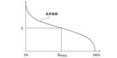
- FIG. 4 is a diagram for explaining a surface load curve and a load area ratio Smr(c) determined in accordance with ISO25178;
- FIG. 4 is a diagram for explaining a level difference Sk of a core portion determined in accordance with ISO25178;
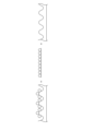
- FIG. 4 is a diagram for explaining that the surface unevenness of the roughening-treated copper foil is composed of roughening particle components and waviness components.
- FIG. 2 is a process flow chart showing an example of a method for manufacturing a printed wiring board according to the present invention, showing initial steps (steps (i) to (iii)).
- FIG. 5 is a process flow chart showing an example of a method for manufacturing a printed wiring board according to the present invention, and shows later steps (steps (iv) to (v)) subsequent to the steps shown in FIG.
- the term “developed area ratio Sdr of the interface” or “Sdr” refers to how much the developed area (surface area) of the defined region increases with respect to the area of the defined region, which is measured in accordance with ISO25178. It is a parameter that expresses whether or not The smaller this value, the more nearly flat the surface shape is, and the Sdr of a completely flat surface is 0%. On the other hand, the larger this value, the more uneven the surface shape.
- the "surface load curve” refers to a curve that represents the height at which the load area ratio is from 0% to 100%, determined in accordance with ISO25178.
- the load area ratio is a parameter representing the area of a region having a certain height c or more, as shown in FIG.
- the load area ratio at height c corresponds to Smr(c) in FIG.
- the secant line of the load curve drawn from the load area ratio of 0% along the load curve with the difference in the load area ratio of 40% is moved from the load area ratio of 0% to the secant line.
- the point where the slope of A straight line that minimizes the sum of squares of deviations in the direction of the vertical axis with respect to the central portion is called an equivalent straight line.
- a portion included in the height range of 0% to 100% of the load area ratio of the equivalent straight line is called a core portion.
- a portion higher than the core portion is called a protruding peak portion, and a portion lower than the core portion is called a protruding valley portion.
- the “core portion level difference Sk” or “Sk” is the value obtained by subtracting the minimum height from the maximum height of the core portion measured in accordance with ISO 25178, and is shown in FIG. It is a parameter calculated from the difference in the height of the equivalent straight line between the load area ratio of 0% and 100%.
- Sdr and Sk can be calculated by measuring the surface profile of a predetermined measurement area on the roughened surface with a commercially available laser microscope.
- Sdr shall be measured under conditions of 200 times magnification, no S filter, and 5 ⁇ m L filter.
- Sk is measured under the conditions of 200 times magnification, no S filter, and no L filter.
- preferable measurement conditions and analysis conditions for the surface profile by the laser microscope will be shown in Examples described later.
- the "electrode surface” of the electrolytic copper foil refers to the surface that was in contact with the cathode when the electrolytic copper foil was manufactured.
- the "deposition surface" of the electrolytic copper foil refers to the surface on which electrolytic copper is deposited during the production of the electrolytic copper foil, that is, the surface that is not in contact with the cathode.
- the copper foil of the present invention is a roughened copper foil.
- This roughened copper foil has a roughened surface on at least one side.
- This roughened surface has a developed area ratio Sdr of the interface of 70.0% or less.
- Sdr developed area ratio
- EBSD electron beam backscatter diffraction
- the developed area ratio Sdr of the interface on the roughened surface is controlled within a predetermined range, and the grain boundaries of the crystal grains of a predetermined orientation existing on the surface opposite to the roughened surface
- excellent transmission characteristics can be achieved in a copper-clad laminate or printed wiring board manufactured using this.
- the mechanism that enables the configuration of the present invention to achieve excellent transmission characteristics is not necessarily clear, it is thought to be as follows.
- the unevenness of the roughened surface consists of a "roughening particle component” and a "waviness component” having a longer period than the roughening particle component.
- the roughened particle component and the waviness component can be distinguished by using an S filter and an L filter of a laser microscope.
- the developed area ratio Sdr of the interface in the present invention more accurately reflects the shape of the roughened particles on the roughened surface of the copper foil.
- a process for improving the reliability is a process of partially dissolving (etching) and roughening the circuit surface.
- etching partially dissolving
- the roughening treatment by etching is performed after the circuit is formed, it is the surface of the circuit that is not in contact with the resin base material that is affected by this treatment, that is, the roughened surface of the roughened copper foil. and the opposite side.
- the dissolution of a polycrystalline metal structure proceeds along the portions (grain boundaries) where crystal grains are in contact with each other. Therefore, the fewer the grain boundaries of the crystal grains existing on the circuit surface, the fewer the portions that are strongly etched, and the transmission characteristics are relatively better than when there are many grain boundaries.
- the number of atoms in contact with the etchant varies depending on the orientation of crystals existing on the surface to be etched, and it is considered that the more atoms that are in contact with the etchant at the same time, the more efficiently the atoms are dissolved. For this reason, it can be said that crystal grains with a small deviation angle (tilt angle) from the (111) plane, which is the closest-packed structure, dissolve particularly quickly.
- tilt angle tilt angle
- the roughened copper foil of the present invention focuses on crystal grains having a deviation angle of 20 degrees or less from the (111) plane, which has a large effect on etching, on the surface opposite to the roughened surface.
- the average value of L/S which is the ratio of the grain boundary length L to the occupied area S of the crystal grains, is controlled to 13.0 ⁇ m/ ⁇ m 2 or less. That is, the roughened copper foil that satisfies the above parameters has few grain boundaries of particles with a small angle of deviation from the (111) plane, which dissolves particularly quickly, so that there are few places that are locally etched quickly. As a result, the surface shape of the circuit becomes smooth after the roughening treatment by etching, and the transmission characteristics can be improved.
- the roughened surface of the roughened copper foil has an interface developed area ratio Sdr of 70.0% or less, preferably 5.0% or more and 60.0% or less, more preferably 10.0% or more and 50.0%. 0% or less, more preferably 20.0% or more and 45.0% or less.
- Sdr interface developed area ratio
- the roughened surface has a richly uneven shape that is convenient for achieving excellent transmission characteristics while ensuring high adhesion to the resin substrate.
- the roughened surface of the roughened copper foil preferably has a core level difference Sk of 1.70 ⁇ m or less, more preferably 0.10 ⁇ m or more and 1.50 ⁇ m or less, and still more preferably 0.50 ⁇ m or more. 40 ⁇ m or less, particularly preferably 0.90 ⁇ m or more and 1.20 ⁇ m or less.
- Sk in the present invention is a parameter obtained by measuring the copper foil surface without an L filter, which more accurately reflects the overall surface shape of the copper foil. It becomes a thing. In this regard, when the Sk is within the above range, the anchor effect is effectively exhibited, and the circuit formability can be improved while ensuring high adhesion to the resin substrate.
- the surface opposite to the roughened surface of the roughened copper foil has an average L/S value of 13.0 ⁇ m/ ⁇ m 2 or less, preferably 2.0 ⁇ m/ ⁇ m 2 or more and 11.0 ⁇ m/ ⁇ m 2 or less. , more preferably 3.0 ⁇ m/ ⁇ m 2 or more and 10.0 ⁇ m/ ⁇ m 2 or less, still more preferably 5.0 ⁇ m/ ⁇ m 2 or more and 9.0 ⁇ m/ ⁇ m 2 or less. If the average value of L / S is within the above range, it is possible to suppress portions that are locally etched quickly while allowing roughening due to etching to proceed appropriately. Therefore, roughening treatment by etching is performed after circuit formation. When this is done, the surface shape of the circuit becomes smooth and the transmission loss can be reduced while improving the reliability which is the original purpose.
- the surface opposite to the roughened surface of the roughened copper foil has a total area A 2 , the sum of the total occupied area A 3 of crystal grains with a deviation angle of 20 degrees or less from the (010) plane and the total occupied area A 4 of crystal grains with a deviation angle of 20 degrees or less from the (001) plane (A 2 + A 3 + A 4 ), and A 1 /(A 2 + A 3 + A 4 ), which is the ratio of the total occupied area A 1 of the crystal grains whose deviation angle from the (111) plane is 20 degrees or less, is 0.10 or more and 0 It is preferably 0.60 or less, more preferably 0.15 or more and 0.55 or less, still more preferably 0.20 or more and 0.50 or less.
- the average value of L / S and A 1 / (A 2 + A 3 + A 4 ) on the surface opposite to the roughened surface of the roughened copper foil are obtained by heating the roughened copper foil at 180 ° C. for 1 hour. It can be specified by analyzing by electron beam backscatter diffraction (EBSD) after it has been processed. Analysis by electron beam backscatter diffraction (EBSD) can be preferably performed according to the procedure shown in the examples described later. The reason why the EBSD analysis is performed after heating the roughened copper foil at 180° C. for 1 hour is as follows.
- the surface opposite to the roughened surface of the roughened copper foil is controlled by the above parameters because after the circuit is formed, when the roughening treatment is performed by etching, the circuit surface is To provide a smooth shape with excellent transmission characteristics.
- Circuit formation is generally carried out in a form in which a roughened copper foil and a resin base material are joined together by hot pressing (that is, in the form of a copper-clad laminate).
- the state of the crystals forming the copper foil can change depending on the heat load. Therefore, by performing EBSD analysis after heating the roughened copper foil under the above conditions, it is possible to evaluate crystal grains in a state close to immediately before the roughening treatment by etching.
- the thickness of the roughened copper foil is not particularly limited, but is preferably 0.1 ⁇ m or more and 210 ⁇ m or less, more preferably 0.3 ⁇ m or more and 105 ⁇ m or less, still more preferably 7 ⁇ m or more and 70 ⁇ m or less, and particularly preferably 15 ⁇ m or more and 20 ⁇ m or less.
- the roughened copper foil of the present invention is not limited to the ordinary copper foil whose surface has been roughened, but the copper foil surface of the carrier-attached copper foil has been roughened or finely roughened. can be anything.
- the roughened copper foil of the present invention is formed by roughening a smooth copper foil surface (for example, the electrode surface of an electrolytic copper foil) under desired low-roughening conditions to form fine roughened particles. It can be produced preferably by Therefore, according to a preferred aspect of the present invention, the roughened copper foil is an electrolytic copper foil, and the roughened surface is present on the electrode surface side of the electrolytic copper foil.
- the roughened copper foil may have roughened surfaces on both sides, or may have a roughened surface only on one side.
- the roughened surface typically comprises a plurality of roughening particles, each of which preferably comprises a metal, more preferably copper.
- the metal forming the roughening particles may contain unavoidable impurities resulting from raw material components, forming processes, and the like.
- the copper may be metallic copper or a copper alloy.
- Electrodeposited copper foil is preferably produced by electrolytic deposition using a copper electrolyte from which polymer compounds such as glue have been removed.
- polymer compounds such as glue are likely to be incorporated into the copper foil and tend to inhibit crystal growth due to heat. Therefore, by using a copper electrolyte from which a polymer compound has been removed, it becomes easier to satisfy the parameters required for the roughened copper foil of the present invention. For example, by treating the copper electrolyte with activated carbon, the polymer compound in the copper electrolyte can be removed.
- R N C ⁇ U/m
- R N is the non-metallic impurity supply ratio (-)
- C is the non-metallic impurity concentration (g/m 3 )
- U is the liquid supply flow rate (m 3 /s)
- m is the copper deposition rate (g/s ) is
- the nonmetallic impurity supply ratio RN defined by is preferably 0.020 or more and 0.100 or less, more preferably 0.030 or more and 0.100 or less.
- the nonmetallic impurity concentration C is a value calculated from the sum of the total organic carbon content (TOC) and the chloride ion ( Cl- ) concentration in the copper electrolyte
- RN is within the above range, chlorine, low-molecular-weight organic substances, etc. can be supplied within a suitable speed range for the deposition of the copper foil.
- the roughness of the deposition surface of the electrodeposited copper foil can be controlled within an appropriate range, and the parameters required for the roughened copper foil of the present invention can be easily satisfied.
- the roughening treatment for forming the roughened surface can be preferably carried out by forming roughening particles with copper or a copper alloy on the copper foil.
- the copper foil before the roughening treatment may be a non-roughened copper foil or a pre-roughened copper foil.
- the surface of the copper foil to be roughened preferably has a ten-point average roughness Rz measured in accordance with JIS B0601-1994 of 0.50 ⁇ m or more and 15.00 ⁇ m or less, more preferably It is 0.50 ⁇ m or more and 2.00 ⁇ m or less. Within the above range, it becomes easier to impart the surface profile required for the roughened copper foil of the present invention to the roughened surface.
- the roughening treatment is performed, for example, in a copper sulfate solution containing a copper concentration of 7 g/L or more and 17 g/L or less and a sulfuric acid concentration of 50 g/L or more and 200 g/L or less at a temperature of 20° C. or more and 40° C. or less at 2.00 A/dm 2 .
- Electrodeposition is preferably carried out at 50 A/dm 2 or less. This electrolytic deposition is preferably carried out for 0.5 seconds to 30 seconds, more preferably 1 second to 30 seconds, and even more preferably 1 second to 5 seconds.
- the roughened copper foil according to the present invention is not limited to the method described above, and may be manufactured by any method.
- R L L/D C (Wherein, R L is the liquid resistance index (mm L/mol), L is the distance between the electrodes (anode-cathode) (mm), and D C is the charge carrier density (mol/L).)
- the liquid resistance index RL defined by is preferably 9.0 mm L / mol or more and 20.0 mm L / mol or less, and 11.0 mm L / mol or more and 17.0 mm L / mol or less is more preferred.
- the bumps can be preferably formed in a shape suitable for imparting the surface profile required for the roughened copper foil of the present invention.
- the charge carrier density Dc can be calculated by totaling the product of each ion concentration and valence for all ions present in the plating solution.
- the liquid resistance index is an index that correlates with the resistance of the solution.
- the roughening treatment may include a second roughening treatment in which electrolytic deposition is performed under predetermined conditions on the surface after the roughening treatment (first roughening treatment). It may further include a third roughening treatment in which electrolytic deposition is performed under predetermined conditions on the surface after the second roughening treatment.
- first roughening treatment in which electrolytic deposition is performed under predetermined conditions on the surface after the roughening treatment.
- third roughening treatment in which electrolytic deposition is performed under predetermined conditions on the surface after the second roughening treatment.
- the preferred conditions for the second roughening treatment the preferred conditions described above for the first roughening treatment apply as they are.
- the third roughening treatment for example, in a copper sulfate solution containing a copper concentration of 65 g/L or more and 80 g/L or less and a sulfuric acid concentration of 50 g/L or more and 200 g/L or less, at a temperature of 45 ° C. or more and 55 ° C. or less, 1 A /dm 2 or more and 5 A/dm 2 or less.
- This electrolytic deposition is preferably carried out for 1 to 10 seconds, more preferably 5 to 8 seconds.
- the liquid resistance index RL is preferably 2.0 mm ⁇ L/mol or more and 9.0 mm ⁇ L/mol or less, and more preferably 5.0 mm ⁇ L/mol or more and 8.0 mm ⁇ L/mol. mol or less is more preferable.
- the roughened copper foil may be subjected to antirust treatment and may have an antirust treatment layer formed thereon.
- the antirust treatment preferably includes plating with zinc.
- the plating treatment using zinc may be either zinc plating treatment or zinc alloy plating treatment, and the zinc alloy plating treatment is particularly preferably zinc-nickel alloy treatment.
- the zinc-nickel alloy treatment may be a plating treatment containing at least Ni and Zn, and may further contain other elements such as Sn, Cr, Co and Mo.
- the antirust treatment layer further contains Mo in addition to Ni and Zn, so that the treated surface of the roughened copper foil has excellent adhesion to resin, chemical resistance, and heat resistance, and etching residue is removed. It becomes difficult to remain.
- Ni/(Zn+Ni) which is the ratio of the Ni deposition amount to the total amount of the Zn deposition amount and the Ni deposition amount, is preferably 0.3 or more and 0.9 or less, more preferably It is 0.4 or more and 0.9 or less, more preferably 0.4 or more and 0.8 or less.
- the total amount of Zn and Ni deposited in the zinc-nickel alloy plating is preferably 8 mg/m 2 or more and 160 mg/m 2 or less, more preferably 13 mg/m 2 or more and 130 mg/m 2 or less, and still more preferably 19 mg/m 2 . 80 mg/ m2 or less.
- Ni/(Zn+Ni+Mo) which is the ratio of the Ni deposition amount to the total amount of the Zn deposition amount, the Ni deposition amount and the Mo deposition amount, is 0.20 or more and 0.20 to 0.20. It is preferably 80 or less, more preferably 0.25 or more and 0.75 or less, still more preferably 0.30 or more and 0.65 or less.
- the total deposition amount of Zn, Ni and Mo in the zinc-nickel-molybdenum alloy plating is preferably 10 mg/m 2 or more and 200 mg/m 2 or less, more preferably 15 mg/m 2 or more and 150 mg/m 2 or less, further preferably 20 mg/m 2 or more and 90 mg/m 2 or less.
- the amounts of Zn, Ni, and Mo deposited were obtained by dissolving a predetermined area (for example, 25 cm 2 ) on the roughened surface of the roughened copper foil with acid, and measuring the concentration of each element in the resulting solution by ICP emission spectrometry. It can be calculated by analyzing based on the law.
- the antirust treatment preferably further includes chromate treatment, and this chromate treatment is more preferably performed on the surface of the zinc-containing plating after the plating treatment using zinc. By doing so, the rust resistance can be further improved.
- a particularly preferred antirust treatment is a combination of zinc-nickel alloy plating treatment (or zinc-nickel-molybdenum alloy plating treatment) and subsequent chromate treatment.
- the surface of the roughened copper foil may be treated with a silane coupling agent to form a silane coupling agent-treated layer.
- a silane coupling agent-treated layer can be formed by appropriately diluting a silane coupling agent, coating it, and drying it.
- silane coupling agents include epoxy-functional silane coupling agents such as 4-glycidylbutyltrimethoxysilane, 3-glycidoxypropyltrimethoxysilane, or 3-aminopropyltriethoxysilane, N-(2- aminoethyl)-3-aminopropyltrimethoxysilane, N-3-(4-(3-aminopropoxy)butoxy)propyl-3-aminopropyltrimethoxysilane, N-phenyl-3-aminopropyltrimethoxysilane, etc.
- epoxy-functional silane coupling agents such as 4-glycidylbutyltrimethoxysilane, 3-glycidoxypropyltrimethoxysilane, or 3-aminopropyltriethoxysilane, N-(2- aminoethyl)-3-aminopropyltrimethoxysilane, N-3-(4-(3-aminopropoxy)but
- amino-functional silane coupling agents or mercapto-functional silane coupling agents such as 3-mercaptopropyltrimethoxysilane or olefin-functional silane coupling agents such as vinyltrimethoxysilane, vinylphenyltrimethoxysilane, or 3-methacrylic acrylic functional silane coupling agents such as roxypropyltrimethoxysilane, 3-acryloxypropyltrimethoxysilane, or imidazole functional silane coupling agents such as imidazole silane, or triazine functional silane coupling agents such as triazine silane, and the like. is mentioned.
- the roughened copper foil preferably has an anticorrosive layer and/or a silane coupling agent-treated layer on the roughened surface, more preferably an anticorrosive layer and a silane coupling agent-treated layer.
- an anticorrosive layer and/or a silane coupling agent-treated layer are formed on the roughened surface.
- the numerical values of Sdr and Sk in this specification refer to the rust-preventive treatment layer and/or the silane coupling agent-treated layer. shall mean a numerical value obtained by measuring and analyzing the surface of the roughened copper foil after is formed.
- the anticorrosion treatment layer and the silane coupling agent treatment layer may be formed not only on the roughened surface side of the roughened copper foil, but also on the side where the roughened surface is not formed.
- a copper-clad laminate includes a resin layer and a roughened copper foil provided on at least one surface of the resin layer.
- This roughened copper foil has a roughened surface on at least one side, and the roughened surface is in contact with the resin layer.
- the roughened surface of the roughened copper foil has an interface developed area ratio Sdr of 70.0% or less.
- the surface opposite to the roughened surface of the roughened copper foil is calculated for each crystal grain having a deviation angle of 20 degrees or less from the (111) plane in the observation field when analyzed by EBSD.
- the average value of L/S which is the ratio of the grain boundary length L to the occupied area S, is 13.0 ⁇ m/ ⁇ m 2 or less. According to this copper-clad laminate, excellent transmission characteristics can be achieved as described above.
- the resin layer of the copper-clad laminate contains resin, preferably insulating resin.
- the resin layer is preferably prepreg and/or resin sheet.
- Prepreg is a general term for composite materials in which synthetic resin is impregnated into a base material such as a synthetic resin plate, a glass plate, a glass woven fabric, a glass non-woven fabric, or paper.
- Preferred examples of insulating resins include epoxy resins, cyanate resins, bismaleimide triazine resins (BT resins), polyphenylene ether resins, and phenol resins.
- Examples of the insulating resin forming the resin sheet include insulating resins such as epoxy resins, polyimide resins, and polyester resins.
- the resin layer may contain filler particles made of various inorganic particles such as silica and alumina from the viewpoint of improving insulation.
- the thickness of the resin layer is not particularly limited, it is preferably 1 ⁇ m or more and 1000 ⁇ m or less, more preferably 2 ⁇ m or more and 400 ⁇ m or less, and still more preferably 3 ⁇ m or more and 200 ⁇ m or less.
- the resin layer may be composed of multiple layers. A resin layer such as a prepreg and/or a resin sheet may be provided on the roughened copper foil in advance via a primer resin layer that is applied to the surface of the copper foil.
- the roughened copper foil included in the copper-clad laminate has a developed area ratio Sdr of the interface on the roughened surface of 70.0% or less, preferably 5.0% or more and 60.0% or less, more preferably 10%. 0% or more and 50.0% or less, more preferably 20.0% or more and 45.0% or less.
- the roughened surface of the roughened copper foil preferably has a core level difference Sk of 1.70 ⁇ m or less, more preferably 0.10 ⁇ m or more and 1.50 ⁇ m or less, and still more preferably 0.50 ⁇ m or more. 1.40 ⁇ m or less, particularly preferably 0.90 ⁇ m or more and 1.20 ⁇ m or less.
- the surface opposite to the roughened surface of the roughened copper foil has an average L/S value of 13.0 ⁇ m/ ⁇ m 2 or less, preferably 2.0 ⁇ m/ ⁇ m 2 or more and 11.0 ⁇ m/ ⁇ m 2 or less. , more preferably 3.0 ⁇ m/ ⁇ m 2 or more and 10.0 ⁇ m/ ⁇ m 2 or less, still more preferably 5.0 ⁇ m/ ⁇ m 2 or more and 9.0 ⁇ m/ ⁇ m 2 or less.
- the surface opposite to the roughened surface of the roughened copper foil is the total occupied area of crystal grains with a deviation angle of 20 degrees or less from the (100) plane in the observation field when analyzed by EBSD.
- a 2 the sum of the total occupied area A 3 of crystal grains with a deviation angle of 20 degrees or less from the (010) plane, and the total occupied area A 4 of crystal grains with a deviation angle of 20 degrees or less from the (001) plane ( A 1 / (A 2 + A 3 + A 4 ), which is the ratio of the total occupied area A 1 of the crystal grains whose deviation angle from the (111) plane is 20 degrees or less to A 2 + A 3 + A 4 ), is 0.10 or more . It is preferably 0.60 or less, more preferably 0.15 or more and 0.55 or less, and still more preferably 0.20 or more and 0.50 or less.
- the roughened copper foil of the present invention is typically used as it is as the roughened copper foil included in the copper-clad laminate. Therefore, the preferred aspects of the roughened copper foil of the present invention apply as they are to the preferred aspects of the roughened copper foil included in the copper-clad laminate.
- the roughened copper foil included in the copper-clad laminate may be any suitable modification of the roughened copper foil of the present invention as long as it satisfies the above parameters.
- the roughened copper foil or copper-clad laminate of the present invention is preferably used for producing a printed wiring board. That is, according to a preferred aspect of the present invention, a method for manufacturing a printed wiring board is provided. This method includes (1) preparation of a roughened copper foil, (2) preparation of a copper clad laminate, (3) formation of a circuit, (4) roughening treatment by etching, and (5) resin including each step of lamination. Each of steps (1) to (5) will be described below with reference to FIGS.
- a roughened copper foil 10 is prepared.
- the roughened copper foil 10 has a roughened surface 10a on at least one side.
- the roughened surface 10a has an interface developed area ratio Sdr of 70.0% or less, preferably 5.0% or more and 60.0% or less, more preferably 10.0% or more and 50.0% or less, More preferably, it is 20.0% or more and 45.0% or less.
- Sdr is within the above range, the shape is rich in unevenness, which is convenient for achieving excellent transmission characteristics while ensuring high adhesion to the resin layer, which will be described later.
- the roughened surface 10a of the roughened copper foil 10 preferably has a core level difference Sk of 1.70 ⁇ m or less, more preferably 0.10 ⁇ m or more and 1.50 ⁇ m or less, and still more preferably 0.50 ⁇ m or more. 1.40 ⁇ m or less, particularly preferably 0.90 ⁇ m or more and 1.20 ⁇ m or less.
- the lamination of the roughened copper foil 10 and the resin layer 12 is preferably performed by hot pressing.
- the heat load conditions (temperature, time, etc.) of hot pressing may be appropriately determined according to the type of resin, and are not particularly limited. Preferred aspects of the resin layer 12 are as described above for the copper-clad laminate.
- the roughened copper foil 10 of the copper-clad laminate 14 is processed to form the circuit 16 .
- the processing of the roughened copper foil 10 may be performed based on a known technique, and is not particularly limited. For example, a subtractive method, a semi-additive method (SAP), a modified semi-additive method (MSAP), or the like can be used to form the circuit 16 with a predetermined pattern.
- SAP semi-additive method
- MSAP modified semi-additive method
- the surface of the circuit 16 before the roughening treatment by etching is calculated for each crystal grain having a deviation angle of 20 degrees or less from the (111) plane in the observation field when analyzed by EBSD.
- the average value of L/S which is the ratio of the grain boundary length L to the occupied area S, is 13.0 ⁇ m/ ⁇ m 2 or less, preferably 2.0 ⁇ m/ ⁇ m 2 or more and 11.0 ⁇ m/ ⁇ m 2 or less, more preferably 3.0 ⁇ m/ ⁇ m 2 or more and 10.0 ⁇ m/ ⁇ m 2 or less, more preferably 5.0 ⁇ m/ ⁇ m 2 or more and 9.0 ⁇ m/ ⁇ m 2 or less.
- the surface of the circuit 16 before the roughening treatment by etching, which will be described later, is analyzed by EBSD, and the total occupied area A 2 of crystal grains with a deviation angle from the (100) plane of 20 degrees or less in the observation field of view.
- the sum of the total occupied area A 4 of crystal grains with a deviation angle of 20 degrees or less from the (001) plane (A 2 +A 3 +A 4 ) to A 1 /(A 2 +A 3 +A 4 )
- a 1 /(A 2 +A 3 +A 4 ) which is the ratio of the total occupied area A 1 of the crystal grains whose deviation angle from the (111) plane is 20 degrees or less
- the circuit 16 is roughened by etching. By doing so, the surface of the circuit 16 is given a roughened shape 16a. As a result, the reliability (adhesion, heat resistance, etc.) between the circuit 16 and the surrounding resin can be improved when laminating the resin layers, which will be described later.
- the roughening treatment by etching is preferably performed by partially etching the surface of the circuit 16 .
- Etching may be performed based on a known technique, and is not particularly limited.
- Typical etching solutions include a solution containing sulfuric acid and hydrogen peroxide, a solution containing sodium persulfate, and the like. These liquids may contain additives for the purpose of controlling the shape of roughening due to etching and stabilizing the etching rate.
- a resin layer 12' may be further laminated so as to cover the circuit 16 after etching. By doing so, the circuit 16 can be used as an inner layer circuit.
- the material and/or thickness of the resin layer 12' may be the same as or different from that of the resin layer 12'.
- additional circuits and resin layers may be alternately formed on the resin layer 12' to form a multilayer wiring board.
- the method of the present invention can additionally perform a known method generally employed in printed wiring boards as appropriate.
- Examples 1-5 The roughened copper foil of the present invention was manufactured as follows.
- Electrolysis was performed under the conditions of a temperature of 45° C., a current density of 40 A/dm 2 or more and 100 A/dm 2 or less, and a nonmetallic impurity supply ratio shown in Table 1 to obtain an electrolytic copper foil having a thickness of 18 ⁇ m.
- the conditions of the roughening treatment in each stage were as follows. - The first roughening treatment is performed in a copper electrolytic solution for roughening treatment (copper concentration: 7 g / L or more and 17 g / L or less, sulfuric acid concentration: 50 g / L or more and 200 g / L or less, liquid temperature: 30 ° C.) Table 1 Electrolysis was carried out under the liquid resistance index, current density and time conditions shown in , followed by washing with water. - The second roughening treatment is performed by electrolysis under the conditions of liquid resistance index, current density and time shown in Table 1 in a copper electrolytic solution for roughening treatment having the same composition as the first roughening treatment, and washing with water. gone.
- the third roughening treatment is performed in a copper electrolytic solution for roughening treatment (copper concentration: 65 g / L or more and 80 g / L or less, sulfuric acid concentration: 50 g / L or more and 200 g / L or less, liquid temperature: 45 ° C.)
- Table 1 Electrolysis was carried out under the liquid resistance index, current density and time conditions shown in , followed by washing with water.
- the antirust treatment shown in Table 1 was performed on the electrolytic copper foil after the roughening treatment.
- a pyrophosphate bath was used on the roughened surface of the electrolytic copper foil, and the potassium pyrophosphate concentration was 100 g / L, the zinc concentration was 1 g / L, and the nickel concentration was 2 g. /L, a molybdenum concentration of 1 g/L, a liquid temperature of 40° C., and a current density of 0.5 A/dm 2 .
- a pyrophosphate bath was applied to the surface of the electrodeposited copper foil that had not been roughened, and the concentration of potassium pyrophosphate was 80 g/L, the concentration of zinc was 0.2 g/L, the concentration of nickel was 2 g/L, the liquid temperature was 40°C.
- Antirust treatment B (zinc-nickel antirust treatment) was performed at a current density of 0.5 A/dm 2 .
- both surfaces of the electrodeposited copper foil were subjected to the antirust treatment B under the same conditions as the surface of the electrodeposited copper foil not subjected to the roughening treatment in Examples 1 to 4.
- Chromate treatment was performed on both surfaces of the antirust-treated electrolytic copper foil to form a chromate layer on the antirust treatment layer. This chromate treatment was performed under the conditions of a chromic acid concentration of 1 g/L, a pH of 11, a liquid temperature of 25° C. and a current density of 1 A/dm 2 .
- Silane Coupling Agent Treatment The chromate-treated copper foil was washed with water and then immediately treated with a silane coupling agent to adsorb the silane coupling agent onto the chromate layer on the roughened surface.
- This silane coupling agent treatment was carried out by spraying a solution of a silane coupling agent using pure water as a solvent onto the roughened surface by showering for adsorption treatment.
- 3-Aminopropyltrimethoxysilane was used as a silane coupling agent, and its concentration was 3 g/L. After adsorption of the silane coupling agent, water was finally evaporated by an electric heater to obtain a roughened copper foil with a predetermined thickness.
- (a) EBSD measurement A roughened copper foil was heated at 180°C for 1 hour to obtain a copper foil sample for EBSD measurement.
- This copper foil sample was fixed using a predetermined jig so that the surface opposite to the roughened surface (hereinafter referred to as "non-treated surface") was on the outside.
- the non-treated surface of the copper foil sample was subjected to planar milling with a cross-section polisher (CP). This planar milling was performed under conditions of an acceleration voltage of 6 kV and an inclination angle of 5°. Marking and FIB marker processing were performed on the untreated surface of the copper foil sample after flat milling for 10 minutes (equivalent to a thickness of 500 nm) as the outermost surface.
- plane milling may be performed by appropriately changing the conditions according to the roughness of the surface of the copper foil to the extent that the EBSD measurement described later becomes possible.
- EBSD measurement becomes possible means that the hit rate in EBSD measurement is 70% or more.
- the hit rate is the ratio of the area that the electron beam hits the sample surface appropriately and can be measured, out of the total area of the sample.
- a hit rate of 70% or more means that the electron beam hits the entire copper foil surface during observation using a scanning electron microscope, and as a result, appropriate EBSD data is obtained.
- the surface of the copper foil sample after plane milling was observed using an FE gun-type scanning electron microscope (Carl Zeiss, Crossbeam 540) equipped with an EBSD detector (Oxford Instruments, Symmetry). . Then, EBSD data was obtained using EBSD measurement software (AZtec 5.0 HF1 manufactured by Oxford Instruments), and the obtained EBSD data was converted to OIM format.
- the measurement conditions of the scanning electron microscope during observation were as follows. Note that the measurement magnification was selected from among 1000 times and 3000 times, the magnification at which 700 or more particles (crystal grains) were detected in the field of view, and which was as high as possible.
- the value of ⁇ thus calculated was 90 degrees or more and less than 180 degrees
- the value obtained by subtracting the value from 180 degrees was adopted as the final value of ⁇ .
- ⁇ was calculated to be 150 degrees by the above formula
- 30 degrees obtained by subtracting it from 180 degrees was adopted as the final value of ⁇ .
- particles with an angle of deviation from the (111) plane of 20 degrees or less, particles with an angle of deviation from the (100) plane of 20 degrees or less, particles with an angle of deviation from the (010) plane of 20 degrees or less, and (001) ) were identified for each particle with a deviation angle of 20 degrees or less from the plane.
- a base material for high frequency (MEGTRON6N manufactured by Panasonic) was prepared as an insulating resin base material.
- a roughened copper foil is laminated on both sides of this insulating resin substrate so that the roughened surface is in contact with the insulating resin substrate, and a vacuum press is used at a temperature of 190 ° C. for a pressing time of 120 minutes. to obtain a copper-clad laminate having an insulation thickness of 136 ⁇ m.
- One surface of the obtained copper-clad laminate was etched to obtain a circuit board having a circuit formed thereon.
- the circuit of the circuit board was subjected to roughening treatment using an etchant containing sulfuric acid-hydrogen peroxide as a main component.
- This roughening treatment was performed by applying the etching conditions in Example 4 where the average amount of reduction in copper thickness was 1.5 ⁇ m to all of Examples 1-5.
- the insulating resin base material was laminated on the circuit-side surface of the circuit board after the roughening treatment, and hot pressing was performed using a vacuum press under conditions of a temperature of 190° C. and a pressing time of 120 minutes. In this way, a transmission loss measuring substrate having a total insulation thickness of 254 ⁇ m (a portion without a circuit) and a stripline having a characteristic impedance of 50 ⁇ was obtained.
- the transmission loss (dB/cm) at 50 GHz was measured on the obtained transmission loss measuring board using a network analyzer (N5225B manufactured by Keysight Technologies).
- Transmission loss is -0.55 dB/cm or more -Bad: Transmission loss is less than -0.55 dB/cm
Landscapes
- Engineering & Computer Science (AREA)
- Chemical & Material Sciences (AREA)
- Microelectronics & Electronic Packaging (AREA)
- Materials Engineering (AREA)
- Chemical Kinetics & Catalysis (AREA)
- Electrochemistry (AREA)
- Metallurgy (AREA)
- Organic Chemistry (AREA)
- Manufacturing & Machinery (AREA)
- Laminated Bodies (AREA)
- Manufacturing Of Printed Wiring (AREA)
- Parts Printed On Printed Circuit Boards (AREA)
- Electroplating Methods And Accessories (AREA)
Priority Applications (3)
| Application Number | Priority Date | Filing Date | Title |
|---|---|---|---|
| KR1020247007885A KR20240067875A (ko) | 2021-09-30 | 2022-09-27 | 조화 처리 구리박 및 동장 적층판, 그리고 프린트 배선판의 제조 방법 |
| CN202280065412.6A CN118019880A (zh) | 2021-09-30 | 2022-09-27 | 粗糙化处理铜箔及覆铜层叠板、以及印刷电路板的制造方法 |
| JP2023551556A JPWO2023054398A1 (https=) | 2021-09-30 | 2022-09-27 |
Applications Claiming Priority (2)
| Application Number | Priority Date | Filing Date | Title |
|---|---|---|---|
| JP2021161959 | 2021-09-30 | ||
| JP2021-161959 | 2021-09-30 |
Publications (1)
| Publication Number | Publication Date |
|---|---|
| WO2023054398A1 true WO2023054398A1 (ja) | 2023-04-06 |
Family
ID=85782784
Family Applications (1)
| Application Number | Title | Priority Date | Filing Date |
|---|---|---|---|
| PCT/JP2022/036024 Ceased WO2023054398A1 (ja) | 2021-09-30 | 2022-09-27 | 粗化処理銅箔及び銅張積層板、並びにプリント配線板の製造方法 |
Country Status (5)
| Country | Link |
|---|---|
| JP (1) | JPWO2023054398A1 (https=) |
| KR (1) | KR20240067875A (https=) |
| CN (1) | CN118019880A (https=) |
| TW (1) | TWI888754B (https=) |
| WO (1) | WO2023054398A1 (https=) |
Citations (2)
| Publication number | Priority date | Publication date | Assignee | Title |
|---|---|---|---|---|
| WO2020031721A1 (ja) * | 2018-08-10 | 2020-02-13 | 三井金属鉱業株式会社 | 粗化処理銅箔、キャリア付銅箔、銅張積層板及びプリント配線板 |
| JP2021001398A (ja) * | 2019-06-19 | 2021-01-07 | 金居開發股▲分▼有限公司 | ミクロ粗面化した電着銅箔及び銅張積層板 |
Family Cites Families (3)
| Publication number | Priority date | Publication date | Assignee | Title |
|---|---|---|---|---|
| JP5758035B2 (ja) | 2013-08-20 | 2015-08-05 | Jx日鉱日石金属株式会社 | 表面処理銅箔及びそれを用いた積層板、プリント配線板、電子機器、並びに、プリント配線板の製造方法 |
| JP7356209B2 (ja) | 2017-03-31 | 2023-10-04 | Jx金属株式会社 | 表面処理銅箔、樹脂層付き表面処理銅箔、キャリア付銅箔、積層体、プリント配線板の製造方法及び電子機器の製造方法 |
| JP6606317B1 (ja) * | 2018-04-25 | 2019-11-13 | 古河電気工業株式会社 | 表面処理銅箔、銅張積層板、及びプリント配線板 |
-
2022
- 2022-09-27 JP JP2023551556A patent/JPWO2023054398A1/ja active Pending
- 2022-09-27 KR KR1020247007885A patent/KR20240067875A/ko active Pending
- 2022-09-27 CN CN202280065412.6A patent/CN118019880A/zh active Pending
- 2022-09-27 WO PCT/JP2022/036024 patent/WO2023054398A1/ja not_active Ceased
- 2022-09-30 TW TW111137154A patent/TWI888754B/zh active
Patent Citations (2)
| Publication number | Priority date | Publication date | Assignee | Title |
|---|---|---|---|---|
| WO2020031721A1 (ja) * | 2018-08-10 | 2020-02-13 | 三井金属鉱業株式会社 | 粗化処理銅箔、キャリア付銅箔、銅張積層板及びプリント配線板 |
| JP2021001398A (ja) * | 2019-06-19 | 2021-01-07 | 金居開發股▲分▼有限公司 | ミクロ粗面化した電着銅箔及び銅張積層板 |
Also Published As
| Publication number | Publication date |
|---|---|
| TW202323594A (zh) | 2023-06-16 |
| KR20240067875A (ko) | 2024-05-17 |
| CN118019880A (zh) | 2024-05-10 |
| TWI888754B (zh) | 2025-07-01 |
| JPWO2023054398A1 (https=) | 2023-04-06 |
Similar Documents
| Publication | Publication Date | Title |
|---|---|---|
| TWI715417B (zh) | 用於印刷電路板之具有低傳輸損耗的電解銅箔 | |
| CN107532322B (zh) | 粗糙化处理铜箔及印刷电路板 | |
| JP7374298B2 (ja) | 粗化処理銅箔、銅張積層板及びプリント配線板 | |
| WO2022255420A1 (ja) | 粗化処理銅箔、銅張積層板及びプリント配線板 | |
| WO2021157363A1 (ja) | 粗化処理銅箔、キャリア付銅箔、銅張積層板及びプリント配線板 | |
| WO2022202539A1 (ja) | キャリア付銅箔、銅張積層板及びプリント配線板 | |
| JP7259093B2 (ja) | 粗化処理銅箔、キャリア付銅箔、銅張積層板及びプリント配線板 | |
| TWI911416B (zh) | 粗化處理銅箔、附載體銅箔、銅箔積層板及印刷配線板 | |
| TWI888714B (zh) | 粗化處理銅箔、附載體銅箔、銅箔積層板及印刷配線板 | |
| TWI804323B (zh) | 粗化處理銅箔、附載體銅箔、銅箔積層板及印刷配線板 | |
| WO2023054398A1 (ja) | 粗化処理銅箔及び銅張積層板、並びにプリント配線板の製造方法 | |
| US12104265B2 (en) | Roughened copper foil, copper-clad laminate and printed wiring board | |
| TWI808775B (zh) | 粗化處理銅箔、銅箔積層板及印刷佈線板 | |
| TWI808777B (zh) | 粗化處理銅箔、銅箔積層板及印刷佈線板 | |
| TWI805378B (zh) | 粗化處理銅箔、附載體銅箔、銅箔積層板及印刷配線板 | |
| CN117480281A (zh) | 粗糙化处理铜箔、覆铜层叠板和印刷电路板 | |
| TW202244330A (zh) | 粗化處理銅箔、銅箔積層板及印刷佈線板 | |
| CN117441039A (zh) | 粗糙化处理铜箔、覆铜层叠板和印刷电路板 |
Legal Events
| Date | Code | Title | Description |
|---|---|---|---|
| 121 | Ep: the epo has been informed by wipo that ep was designated in this application |
Ref document number: 22876264 Country of ref document: EP Kind code of ref document: A1 |
|
| WWE | Wipo information: entry into national phase |
Ref document number: 2023551556 Country of ref document: JP |
|
| WWE | Wipo information: entry into national phase |
Ref document number: 202280065412.6 Country of ref document: CN Ref document number: 2401002004 Country of ref document: TH |
|
| NENP | Non-entry into the national phase |
Ref country code: DE |
|
| 122 | Ep: pct application non-entry in european phase |
Ref document number: 22876264 Country of ref document: EP Kind code of ref document: A1 |