WO2023054179A1 - Electronic device - Google Patents
Electronic device Download PDFInfo
- Publication number
- WO2023054179A1 WO2023054179A1 PCT/JP2022/035432 JP2022035432W WO2023054179A1 WO 2023054179 A1 WO2023054179 A1 WO 2023054179A1 JP 2022035432 W JP2022035432 W JP 2022035432W WO 2023054179 A1 WO2023054179 A1 WO 2023054179A1
- Authority
- WO
- WIPO (PCT)
- Prior art keywords
- insulating
- circuit board
- electronic device
- housing
- insulating portion
- Prior art date
Links
- 239000012212 insulator Substances 0.000 claims description 21
- 239000000463 material Substances 0.000 abstract description 16
- 239000000758 substrate Substances 0.000 abstract description 14
- 230000015556 catabolic process Effects 0.000 abstract description 7
- 238000009413 insulation Methods 0.000 description 52
- 230000000149 penetrating effect Effects 0.000 description 51
- 125000006850 spacer group Chemical group 0.000 description 18
- 229910052751 metal Inorganic materials 0.000 description 14
- 239000002184 metal Substances 0.000 description 14
- 238000012986 modification Methods 0.000 description 12
- 230000004048 modification Effects 0.000 description 12
- 230000035515 penetration Effects 0.000 description 11
- 208000028659 discharge Diseases 0.000 description 10
- 230000000694 effects Effects 0.000 description 9
- 230000007547 defect Effects 0.000 description 8
- XEEYBQQBJWHFJM-UHFFFAOYSA-N Iron Chemical compound [Fe] XEEYBQQBJWHFJM-UHFFFAOYSA-N 0.000 description 6
- 230000000052 comparative effect Effects 0.000 description 5
- 238000003780 insertion Methods 0.000 description 5
- 230000037431 insertion Effects 0.000 description 5
- 229910000831 Steel Inorganic materials 0.000 description 4
- 229910045601 alloy Inorganic materials 0.000 description 4
- 239000000956 alloy Substances 0.000 description 4
- 229910052782 aluminium Inorganic materials 0.000 description 4
- XAGFODPZIPBFFR-UHFFFAOYSA-N aluminium Chemical compound [Al] XAGFODPZIPBFFR-UHFFFAOYSA-N 0.000 description 4
- 239000010949 copper Substances 0.000 description 4
- 239000003822 epoxy resin Substances 0.000 description 4
- 229920000647 polyepoxide Polymers 0.000 description 4
- 229920005989 resin Polymers 0.000 description 4
- 239000011347 resin Substances 0.000 description 4
- 239000010959 steel Substances 0.000 description 4
- 239000010935 stainless steel Substances 0.000 description 3
- 229910001220 stainless steel Inorganic materials 0.000 description 3
- 229910001369 Brass Inorganic materials 0.000 description 2
- RYGMFSIKBFXOCR-UHFFFAOYSA-N Copper Chemical compound [Cu] RYGMFSIKBFXOCR-UHFFFAOYSA-N 0.000 description 2
- CWYNVVGOOAEACU-UHFFFAOYSA-N Fe2+ Chemical compound [Fe+2] CWYNVVGOOAEACU-UHFFFAOYSA-N 0.000 description 2
- 239000010951 brass Substances 0.000 description 2
- 229910052802 copper Inorganic materials 0.000 description 2
- 230000000977 initiatory effect Effects 0.000 description 2
- 229910052742 iron Inorganic materials 0.000 description 2
- 229920005177 Duracon® POM Polymers 0.000 description 1
- 239000004677 Nylon Substances 0.000 description 1
- ISWSIDIOOBJBQZ-UHFFFAOYSA-N Phenol Chemical compound OC1=CC=CC=C1 ISWSIDIOOBJBQZ-UHFFFAOYSA-N 0.000 description 1
- 239000003990 capacitor Substances 0.000 description 1
- 238000002788 crimping Methods 0.000 description 1
- -1 ferrous metals Chemical class 0.000 description 1
- 239000011521 glass Substances 0.000 description 1
- 230000017525 heat dissipation Effects 0.000 description 1
- 239000012535 impurity Substances 0.000 description 1
- 239000011810 insulating material Substances 0.000 description 1
- 150000002739 metals Chemical class 0.000 description 1
- 229920001778 nylon Polymers 0.000 description 1
- 239000007787 solid Substances 0.000 description 1
- 238000003466 welding Methods 0.000 description 1
Images


Classifications
-
- H—ELECTRICITY
- H01—ELECTRIC ELEMENTS
- H01L—SEMICONDUCTOR DEVICES NOT COVERED BY CLASS H10
- H01L25/00—Assemblies consisting of a plurality of individual semiconductor or other solid state devices ; Multistep manufacturing processes thereof
- H01L25/03—Assemblies consisting of a plurality of individual semiconductor or other solid state devices ; Multistep manufacturing processes thereof all the devices being of a type provided for in the same subgroup of groups H01L27/00 - H01L33/00, or in a single subclass of H10K, H10N, e.g. assemblies of rectifier diodes
- H01L25/04—Assemblies consisting of a plurality of individual semiconductor or other solid state devices ; Multistep manufacturing processes thereof all the devices being of a type provided for in the same subgroup of groups H01L27/00 - H01L33/00, or in a single subclass of H10K, H10N, e.g. assemblies of rectifier diodes the devices not having separate containers
- H01L25/07—Assemblies consisting of a plurality of individual semiconductor or other solid state devices ; Multistep manufacturing processes thereof all the devices being of a type provided for in the same subgroup of groups H01L27/00 - H01L33/00, or in a single subclass of H10K, H10N, e.g. assemblies of rectifier diodes the devices not having separate containers the devices being of a type provided for in group H01L29/00
-
- H—ELECTRICITY
- H01—ELECTRIC ELEMENTS
- H01L—SEMICONDUCTOR DEVICES NOT COVERED BY CLASS H10
- H01L25/00—Assemblies consisting of a plurality of individual semiconductor or other solid state devices ; Multistep manufacturing processes thereof
- H01L25/18—Assemblies consisting of a plurality of individual semiconductor or other solid state devices ; Multistep manufacturing processes thereof the devices being of types provided for in two or more different subgroups of the same main group of groups H01L27/00 - H01L33/00, or in a single subclass of H10K, H10N
-
- H—ELECTRICITY
- H02—GENERATION; CONVERSION OR DISTRIBUTION OF ELECTRIC POWER
- H02M—APPARATUS FOR CONVERSION BETWEEN AC AND AC, BETWEEN AC AND DC, OR BETWEEN DC AND DC, AND FOR USE WITH MAINS OR SIMILAR POWER SUPPLY SYSTEMS; CONVERSION OF DC OR AC INPUT POWER INTO SURGE OUTPUT POWER; CONTROL OR REGULATION THEREOF
- H02M3/00—Conversion of dc power input into dc power output
-
- H—ELECTRICITY
- H02—GENERATION; CONVERSION OR DISTRIBUTION OF ELECTRIC POWER
- H02M—APPARATUS FOR CONVERSION BETWEEN AC AND AC, BETWEEN AC AND DC, OR BETWEEN DC AND DC, AND FOR USE WITH MAINS OR SIMILAR POWER SUPPLY SYSTEMS; CONVERSION OF DC OR AC INPUT POWER INTO SURGE OUTPUT POWER; CONTROL OR REGULATION THEREOF
- H02M7/00—Conversion of ac power input into dc power output; Conversion of dc power input into ac power output
- H02M7/42—Conversion of dc power input into ac power output without possibility of reversal
- H02M7/44—Conversion of dc power input into ac power output without possibility of reversal by static converters
- H02M7/48—Conversion of dc power input into ac power output without possibility of reversal by static converters using discharge tubes with control electrode or semiconductor devices with control electrode
-
- H—ELECTRICITY
- H05—ELECTRIC TECHNIQUES NOT OTHERWISE PROVIDED FOR
- H05K—PRINTED CIRCUITS; CASINGS OR CONSTRUCTIONAL DETAILS OF ELECTRIC APPARATUS; MANUFACTURE OF ASSEMBLAGES OF ELECTRICAL COMPONENTS
- H05K7/00—Constructional details common to different types of electric apparatus
- H05K7/14—Mounting supporting structure in casing or on frame or rack
Definitions
- This disclosure relates to electronic equipment.
- an insulating plate is arranged between the printed circuit board and a metal housing.
- insulation between the printed circuit board and the metal casing is ensured by the contact of the insulating plate with the printed circuit board and the metal casing.
- the surface of the insulating plate may have irregularities, it is difficult to bring the insulating plate into contact with the printed circuit board without gaps. Defects such as voids and gaps may intervene between the insulating plate and the printed circuit board due to unevenness on the surface of the insulating plate. If dirt or the like adheres to the surface of the insulating plate, the creeping discharge initiation voltage is lowered. When a voltage higher than the start voltage of the creeping discharge is applied, defects such as the voids and gaps become the starting point of the discharge, causing the creeping discharge, which may eventually lead to dielectric breakdown.
- the present disclosure has been made in view of the above problems, and an object thereof is to provide an electronic device capable of suppressing the occurrence of dielectric breakdown.
- the electronic device of the present disclosure includes a circuit board, an insulating plate, a housing, and an insulating support.
- the circuit board includes a conductive member, a first side and a second side.
- a conductive member is arranged on the first surface.
- the second surface faces the first surface.
- the insulating plate is arranged on the side opposite to the first surface with respect to the second surface.
- the housing has electrical conductivity.
- the housing is in contact with the insulating plate on the side opposite to the circuit board with respect to the insulating plate.
- An insulating support supports the circuit board to the insulating plate.
- the insulating support is electrically insulated with respect to the housing.
- the second side of the circuit board is spaced from the insulating plate by an insulating support.
- the second surface of the circuit board is spaced apart from the insulating plate by the insulating support member. Therefore, it is possible to suppress the occurrence of creeping discharge originating from defects such as voids and gaps in the insulating plate. Therefore, it is possible to suppress the occurrence of dielectric breakdown.
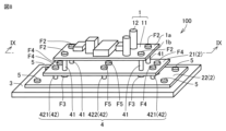
- FIG. 1 is a perspective view schematically showing the configuration of an electronic device according to Embodiment 1;
- FIG. FIG. 2 is a cross-sectional view taken along line II-II of FIG. 1;
- 2 is a plan view schematically showing the configuration of the circuit board of the electronic device according to Embodiment 1;
- FIG. 2 is a plan view schematically showing the configuration of an insulating plate of the electronic device according to Embodiment 1;
- FIG. 2 is a plan view schematically showing the configuration of the circuit board of the electronic device according to Embodiment 1;
- FIG. FIG. 4 is a cross-sectional view schematically showing the configuration of an electronic device according to a modification of Embodiment 1;
- FIG. 3 is a cross-sectional view schematically showing the configuration of an electronic device according to a comparative example
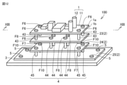
- FIG. 10 is a perspective view schematically showing the configuration of an electronic device according to Embodiment 2
- FIG. 9 is a cross-sectional view taken along line IX-IX of FIG. 8
- FIG. 11 is a plan view schematically showing the configuration of a first insulating portion of an electronic device according to Embodiment 2
- FIG. 8 is a plan view schematically showing the configuration of a second insulating portion of an electronic device according to Embodiment 2
- FIG. 11 is a perspective view schematically showing the configuration of an electronic device according to Embodiment 3
- FIG. 13 is a cross-sectional view along line XIII-XIII of FIG. 12;
- FIG. 11 is a plan view schematically showing the configuration of a third insulating portion of an electronic device according to Embodiment 3;
- FIG. 11 is a plan view schematically showing the configuration of a fourth insulating portion of an electronic device according to Embodiment 3;
- FIG. 11 is a plan view schematically showing the configuration of a fifth insulating portion of an electronic device according to Embodiment 3;
- FIG. 11 is a cross-sectional view schematically showing the configuration of an electronic device according to a first modification of the third embodiment;
- FIG. 12 is a perspective view schematically showing the configuration of an electronic device according to a second modification of the third embodiment;
- FIG. 19 is a cross-sectional view along line XIX-XIX in FIG. 18;
- FIG. 19 is a cross-sectional view along line XIX-XIX in FIG. 18;
- FIG. 21 is a top view schematically showing the configuration of a third insulating portion of an electronic device according to a second modification of the third embodiment
- FIG. 20 is a bottom view schematically showing a configuration of a fourth insulating portion of an electronic device according to a second modified example of the third embodiment
- FIG. 20 is a perspective view schematically showing the configuration of an electronic device according to a third modified example of the third embodiment
- FIG. 23 is a cross-sectional view taken along line XXIII-XXIII of FIG. 22
- FIG. 21 is a side view schematically showing the configuration of an insulating plate and an insulating support member of an electronic device according to a third modification of the third embodiment
- FIG. 20 is a top view schematically showing the configuration of an insulating plate and an insulating supporting member of an electronic device according to a third modification of the third embodiment
- FIG. 12 is a perspective view schematically showing the configuration of an electronic device according to Embodiment 4
- FIG. 27 is a cross-sectional view along line XXVII-XXVII of FIG. 26
- FIG. 11 is a plan view schematically showing the configuration of an insulating plate of an electronic device according to Embodiment 4
- FIG. 12 is a perspective view schematically showing the configuration of an electronic device according to Embodiment 5
- FIG. 30 is a cross-sectional view along line XXX-XXX in FIG. 29;
- FIG. 11 is a plan view schematically showing the configuration of an insulating plate of an electronic device according to Embodiment 5;
- FIG. 11 is a side view schematically showing the configuration of an insulating plate of an electronic device according to Embodiment 5;
- FIG. 11 is a plan view schematically showing the configuration of a housing of an electronic device according to Embodiment 5;
- FIG. 13 is a perspective view schematically showing the configuration of a fixture for electronic equipment according to Embodiment 5;
- Embodiment 1 The configuration of electronic device 100 according to the first embodiment will be described with reference to FIGS. 1 to 5.
- FIG. 1 A diagrammatic representation of electronic device 100 according to the first embodiment will be described with reference to FIGS. 1 to 5.
- electronic device 100 is, for example, a control device.
- Electronic device 100 mainly includes circuit board 1 , insulating plate 2 , housing 3 , insulating support member 4 , and fixing portion 5 .
- the configuration of electronic device 100 will be described using the thickness direction and the in-plane direction.
- the thickness direction crosses the in-plane direction.
- the thickness direction is orthogonal to the in-plane direction.
- the circuit board 1 includes a board portion 11 and a conductive member 12.
- the substrate portion 11 includes a first surface 1a and a second surface 1b.
- a conductive member 12 is mounted on the substrate portion 11 .
- the conductive member 12 has conductivity.
- the conductive member 12 is, for example, an electronic component, an electrical component, a metal wiring pattern, or the like.
- the substrate portion 11 has a flat plate shape.
- a conductive member 12 is arranged on the first surface 1a.
- the second surface 1b faces the first surface 1a.
- the conductive member 12 is not arranged on the second surface 1b.
- the second surface 1b faces the first surface 1a along the thickness direction.
- the circuit board 1 extends along the in-plane direction.
- the board portion 11 is made of a printed board member such as paper phenol, glass epoxy resin, or the like.
- the thickness of the substrate portion 11 is, for example, 0.4 mm or more and 3.2 mm or less.
- the width and length of the substrate portion 11 are, for example, 25 mm or more and 550 mm or less.
- the insulating plate 2 is arranged on the side opposite to the first surface 1a with respect to the second surface 1b.
- the insulating plate 2 has insulating properties.
- the insulating plate 2 is made of, for example, insulating resin such as epoxy resin.
- the insulating plate 2 extends along the in-plane direction.
- the insulating plate 2 has an in-plane dimension larger than that of the circuit board 1 .
- the housing 3 is in contact with the insulating plate 2 on the side opposite to the circuit board 1 with respect to the insulating plate 2 .
- the housing 3 is arranged without leaving an interval from the insulating plate 2 . It is desirable that the housing 3 is in contact with the insulating plate 2 without gaps.
- An insulating plate 2 is fixed to the housing 3 .
- the housing 3 has an in-plane dimension larger than that of the insulating plate 2 .
- the housing 3 has conductivity.
- the housing 3 is made of metal.
- the housing 3 is made of, for example, iron and steel typified by steel and iron-containing alloys.
- the housing 3 is made of, for example, a non-ferrous metal such as an alloy containing a metal such as aluminum (Al) or copper (Cu).
- the insulating support member 4 supports the circuit board 1 on the insulating plate 2 .
- An insulating support member 4 is interposed between the circuit board 1 and the insulating plate 2 .
- the insulating support member 4 has portions exposed from the circuit board 1 and the insulating plate 2 over the entire circumference.
- One end of insulating support member 4 is fixed to circuit board 1 by each of a plurality of first fixtures F1.
- insulating support 4 includes a plurality of spacers 40 .
- the insulating support 4 contains, for example, four spacers 40 .
- Each of the plurality of spacers 40 supports the circuit board 1 on the insulating plate 2 .
- Each of the plurality of spacers 40 has the same shape as each other.
- Each of the plurality of spacers 40 is the same as the insulating support material 4 .
- the insulating support material 4 is electrically insulated from the housing 3.
- the circuit board 1 supported by the insulating support member 4 is also electrically insulated from the housing 3 .
- the other end of the insulating support member 4 is embedded in the insulating plate 2 .
- the other end of the insulating support member 4 does not penetrate the insulating plate 2 .
- the other end of the insulating support member 4 is not in contact with the housing 3 .
- the other end of the insulating support member 4 is electrically insulated from the housing 3 .
- the insulating support member 4 is configured separately from the insulating plate 2 and the housing 3 .
- the insulating support material 4 has insulating properties.
- the insulating support member 4 is made of an insulating material such as Duracon (registered trademark) or nylon.
- the shape of the insulating support member 4 is, for example, linear.
- the insulating support member 4 may be configured as an insulator as described below.
- the second surface 1 b of the circuit board 1 is spaced apart from the insulating plate 2 by the insulating support material 4 .
- the insulating plate 2 is not in contact with the second surface 1 b of the circuit board 1 .
- the entire second surface 1 b of the circuit board 1 is spaced apart from the insulating plate 2 by the insulating support member 4 .
- the circuit board 1 and the insulating plate 2 are connected only through the insulating support member 4 .
- the fixing part 5 fixes the insulating plate 2 to the housing 3 .
- the fixing portion 5 fixes the insulating plate 2 to the housing 3 by mechanically fastening the insulating plate 2 to the housing 3 .
- the fixing portion 5 is configured by, for example, a plurality of rivets 50 (see FIG. 1).
- the fixing portion 5 is a rivet
- the rivet is processed by a riveter tool in a state in which the rivet penetrates the first through portion H1 of the insulating plate 2 and the pilot hole of the housing 3, thereby fixing the insulating plate 2 to the housing. It is fixed to the body 3.
- the fixing portion 5 may be configured by, for example, a plurality of screws.
- the fixing part 5 is a screw
- the housing 3 is provided with a nut in advance by crimping, and the insulating plate 2 is fixed to the housing 3 by screwing the screw to the nut.
- the fixed part 5 has conductivity.
- the fixed portion 5 is made of metal such as aluminum (Al) or stainless steel.
- the fixing part 5 is the same as each of the rivets or each of the screws.
- the fixing part 5 is arranged outside the circuit board 1 when the circuit board 1 and the fixing part 5 are viewed along the direction from the first surface 1a to the second surface 1b.
- the fixing portion 5 is exposed from the circuit board 1 when the fixing portion 5 is viewed along the direction from the first surface 1a to the second surface 1b.
- the creepage distance and the spatial distance from the fixed portion 5 to the conductive member 12 are longer than the creepage distance and the spatial distance from the conductive member 12 to the insulating plate 2 .
- the plurality of first fixtures F1 fix the circuit board 1 to the insulating support member 4.
- the plurality of first fixtures F1 fix the circuit board 1 to the insulating support member 4 by mechanically fastening the circuit board 1 to the insulating support member 4 .
- a plurality of first fixtures F1 are fixed to the insulating support member 4 while passing through the substrate portion 11 .
- Each of the multiple first fixtures F1 is configured by, for example, a screw.
- the screw is, for example, a pan screw, and is made of metal such as iron (Fe), stainless steel, or brass.
- the multiple first fixtures F1 are conductive.
- the circuit board 1 is provided with a plurality of insertion holes IH.
- a first fixture F1 (see FIG. 2) is inserted into each of the plurality of insertion holes IH.
- the plurality of insertion holes IH are configured as female threads.
- Each of the four corners of the circuit board 1 is provided with a plurality of insertion holes IH.
- the insulating plate 2 is provided with a plurality of first penetrating portions H1 and a plurality of first engaging portions E1.
- a fixing portion 5 (see FIG. 2) is inserted into each of the plurality of first penetrating portions H1.
- Each of the four corners of the insulating plate 2 is provided with a plurality of first penetrating portions H1.
- the plurality of first engaging portions E1 do not penetrate the insulating plate 2 .
- the plurality of first engaging portions E1 are configured as screw holes, for example.
- An insulating support member 4 (see FIG. 2) is fixed to each of the plurality of first engaging portions E1.
- the plurality of first penetrating portions H1 are arranged outside the plurality of first engaging portions E1.
- the shortest distance along the surface of the insulating plate 2 from each first penetrating portion H1 to the first engaging portion E1 arranged in the immediate vicinity of the first penetrating portion H1 is The same is true for each of the plurality of first engaging portions E1.
- the housing 3 is provided with a plurality of through holes TH.
- a fixing portion 5 (see FIG. 2) is inserted into each of the plurality of through holes TH.
- Each of the four corners of the housing 3 is provided with a plurality of through holes.
- the insulation distance for insulation between the circuit board 1 and the housing 3 includes a creepage distance and a spatial distance.
- the creepage distance is the shortest distance between the circuit board 1 and the housing 3 via an insulator. In FIG. 2, the creepage distance is indicated by a solid arrow.
- the spatial distance is the shortest distance between the circuit board 1 and the housing 3 through the air. In FIG. 2, the spatial distances are indicated by dashed arrows.
- the creepage distance is the shortest distance f1 along the first surface 1a of the circuit board 1 between the conductive member 12 (metal wiring pattern) of the circuit board 1 and the first fixture F1, It is the sum (f1+a1+g1) of the shortest distance a1 along the surface of the insulating support member 4 to the plate 2 and the shortest distance g1 along the surface of the insulating plate 2 between the insulating support member 4 and the fixed portion 5.
- the shortest distance a1 is also the dimension in the thickness direction of the insulating support member 4 between the circuit board 1 and the insulating plate 2. As shown in FIG.
- the creepage distance in the present embodiment is the shortest creepage distance from conductive member 12 of circuit board 1 to fixed portion 5 via insulating support member 4 and insulating plate 2 .
- the shortest creepage distance of this embodiment is designed to satisfy the creepage distance required by the standard.
- the insulation performance (withstand voltage value) of the electronic device 100 increases as the creepage distance (f1+a1+g1) increases. Therefore, the larger the in-plane dimension of the insulating plate 2, the longer the shortest distance g1 along the surface of the insulating plate 2 between the insulating support member 4 and the fixed portion 5, and the longer the creeping distance (f1+a1+g1). Therefore, the larger the dimension of the insulating plate 2 in the in-plane direction, the higher the insulating performance (withstand voltage value) of the electronic device 100 .
- the spatial distance h1 is the sum of the shortest distance between the fixing portion 5 and the first fixture F1 and the shortest distance between the first fixture F1 and the conductive member 12 of the circuit board 1.
- the creepage distance (f1+a1+g1) is longer than the clearance h1.
- the creepage distance required for insulation between the circuit board 1 and the housing 3 is longer than the spatial distance required for insulation between the circuit board 1 and the housing 3 .
- the spatial distance required for insulation between the circuit board 1 and the housing 3 is h1
- the creepage distance required for insulation between the circuit board 1 and the housing 3 is (1.5 ⁇ h1).
- the circuit board 1 and the housing 3 are insulated if the creepage distance (f1+a1+g1) is (1.5 ⁇ h1) or more.
- the creepage distance and the clearance are increased without increasing the dimension in the thickness direction of the electronic device 100 . That is, the expansion of the dimension of the electronic device 100 in the thickness direction is suppressed while ensuring both the creepage distance and the clearance between the circuit board 1 and the housing 3 and the insulation performance.
- the insulating support material 4 may be configured as an insulator.
- the insulating support member 4 configured as an insulator includes a shaft portion 4a and a plurality of projecting portions 4b projecting from the shaft portion 4a.
- the shortest distance a1 between the circuit board 1 and the insulating plate 2 along the surface of the insulating support member 4 is increased while the thickness dimension of the insulating support member 4 is maintained.
- the insulation performance (withstand voltage value) of the electronic device 100 is increased.
- the standard requires that the creepage distance be longer than the spatial distance, but if the creepage distance is excessively longer than the spatial distance, the electronic device 100 becomes excessively large. That is, if there is an extra length difference between the creepage distance and the spatial distance, the electronic device 100 becomes excessively large. The extra length difference between the creepage distance and the clearance distance is reduced by the insulator.
- the electronic device 101 does not include the insulating plate 2 (see FIG. 2).
- the circuit board 1 is supported by the housing 3 by linear spacers 40 .
- the insulation distance between the circuit board 1 and the housing 3 is maintained by the length L of the spacer 40 .
- JEM Joint Electrical Manufacturers' Association
- the spatial distance is 60 mm or more.
- a creepage distance of 90 mm or more must be secured.
- the length of the spacer 40 is 90 mm in order to satisfy the insulation distance between the circuit board 1 and the housing 3.
- the spatial distance is 60 mm or more
- the linear spacer 40 is used, it is necessary to ensure a creepage distance of 90 mm or more.
- the resonance frequency of the circuit board 1 may be low. Therefore, the resonance frequency of the circuit board 1 may be included in the vibration frequency band of the structure of the electronic device 101 .
- the circuit board 1 When the circuit board 1 resonates with the structure of the electronic device 101, the amplitude of heavy objects such as electronic components mounted on the circuit board 1 may be amplified. As a result, the circuit board 1 vibrates violently, and the circuit board 1 may be destroyed by the vibration. Vibration of the circuit board 1 can occur in the thickness direction and the in-plane direction. Breakage due to vibration of the circuit board 1 on which a heavy object is mounted includes, for example, breakage of connection points between terminals of heavy electronic components such as transformers, capacitors, and reactors and the circuit board 1, breakage of terminals, and the like. That is, the electronic device 101 according to the comparative example has a problem of low vibration resistance.
- a configuration in which the circuit board 1 and the housing 3 are fixed via an insulator may be adopted.
- the creepage distance between the circuit board 1 and the housing 3 is ensured by the uneven structure of the insulator. Therefore, the creepage distance is ensured with an insulator having a length shorter than that of the straight spacer 40 .
- the in-plane dimension of the circuit board 1 needs to be further increased. That is, when the insulation distance is ensured only by the insulator, there is a problem that the dimension of the electronic device in the in-plane direction becomes large due to the above.
- second surface 1b of circuit board 1 is spaced apart from insulating plate 2 by insulating support member 4. there is Therefore, the insulating distance between the circuit board 1 and the housing 3 is ensured by the combination of the insulating plate 2 and the insulating support member 4 . Therefore, it is possible to suppress the dimension of the electronic device 100 from increasing in the thickness direction as compared with the case where the insulation distance is secured only by the linear spacer 40 (see FIG. 7), and the case where the insulation distance is secured only by the insulator. It is possible to prevent the in-plane dimension of the electronic device 100 from increasing.
- the natural frequency of the circuit board 1 can be increased, and the natural frequency of the circuit board 1 can be made different from the vibration frequency in the structure of the electronic device 100, so that the vibration resistance of the circuit board 1 can be improved. be able to.
- outside air can flow in the space between the second surface 1b of the circuit board 1 and the insulating plate 2, heat dissipation from the conductive member 12 mounted on the circuit board 1 can be realized.
- air exists between the second surface 1b of the circuit board 1 and the insulating plate 2 the risk of discharge and creeping discharge caused by voids is reduced.
- the second surface 1 b of the circuit board 1 is spaced apart from the insulating plate 2 by the insulating support member 4 . Therefore, the second surface 1b of the circuit board 1 and the insulating plate 2 do not come into contact with each other. If it is necessary to bring the entire second surface 1b of the circuit board 1 into contact with the insulating plate 2, defects such as voids and gaps may occur between the second surface 1b and the insulating plate 2, causing defects. Such partial discharge may occur, the insulating plate 2 may deteriorate, and dielectric breakdown may occur. Further, if the insulating plate 2 in contact with the second surface 1b of the circuit board 1 contains impurities, the creeping discharge initiating voltage is reduced.
- a creeping discharge caused by the defect may occur, and dielectric breakdown may occur.
- the electronic device 100 according to the present embodiment it is not necessary to bring the second surface 1b of the circuit board 1 and the insulating plate 2 into contact with each other. It is possible to suppress the occurrence of defects such as voids and voids. Therefore, it is possible to suppress the occurrence of dielectric breakdown caused by defects in the insulating plate 2 .
- the fixing portion 5 is arranged outside the circuit board 1 when the circuit board 1 and the fixing portion 5 are viewed along the direction from the first surface 1a to the second surface 1b. ing. Therefore, the spatial distance h1 between the circuit board 1 and the housing 3 can be made larger than when the fixing portion 5 is arranged inside the circuit board 1 . Further, for example, the spatial distance h1 between the circuit board 1 and the housing 3 can be made larger than when the circuit board 1 and the housing 3 are connected by a linear spacer 40 (see FIG. 7). . Therefore, the insulation performance (withstand voltage value) of the housing 3 can be improved.
- Embodiment 2 Next, the configuration of electronic device 100 according to the second embodiment will be described with reference to FIGS. 8 to 11.
- FIG. The second embodiment has the same configuration and effects as those of the first embodiment unless otherwise specified. Therefore, the same reference numerals are given to the same configurations as in the above-described first embodiment, and description thereof will not be repeated.
- the insulating plate 2 of the electronic device 100 includes a first insulating portion 21 and a second insulating portion 22 .
- the first insulating portion 21 is connected to the circuit board 1 .
- the second insulating portion 22 is in contact with the housing 3 .
- the first insulating portion 21 and the second insulating portion 22 are viewed along the direction from the first surface 1a to the second surface 1b, the first insulating portion 21 and the second insulating portion 2
- the insulating part 22 is larger than the circuit board 1 .
- the first insulating portion 21 and the second insulating portion 22 have an area larger than that of the circuit board 1 .
- the second insulating portion 22 is larger than the first insulating portion 21 when the first insulating portion 21 and the second insulating portion 22 are viewed along the direction from the first surface 1a toward the second surface 1b.
- the second insulating portion 22 has an area larger than that of the first insulating portion 21 .
- the insulating support member 4 includes a first support portion 41 and a second support portion 42 .
- the first supporting portion 41 supports the circuit board 1 on the first insulating portion 21 .
- the first support portion 41 and the second support portion 42 include a plurality of spacers.
- One end of the first support portion 41 is fixed to the circuit board 1 by each of the plurality of second fixtures F2.
- the other end of the first support portion 41 is fixed to the first insulating portion 21 by each of the plurality of third fixtures F3.
- the first support portion 41 and the second support portion 42 are the same as each of the plurality of spacers.
- the second supporting portion 42 supports the first insulating portion 21 on the second insulating portion 22 .
- the second support portion 42 is arranged to be displaced from the first support portion 41 in the in-plane direction.
- the second support portion 42 is not arranged on the same imaginary straight line extending in the thickness direction with respect to the first support portion 41 .
- the second support portion 42 has a first portion 421 and a second portion 422 .
- Each of the first portion 421 and the second portion 422 supports the first insulating portion 21 to the second insulating portion 22 .
- One end of the first portion 421 is fixed to the first insulating portion 21 by each of the plurality of fourth fixtures F4.
- One end of the second portion 422 is fixed to the first insulating portion 21 by each of the plurality of fifth fixtures F5.
- the other end of the first portion 421 and the other end of the second portion 422 are fixed to the second insulating portion 22 by being screwed into the second insulating portion 22 .
- the first portion 421 extends outside the circuit board 1 .
- the second portion 422 is arranged inside the circuit board 1 , and the first support portion 41 is arranged so as to be sandwiched between the first portion 421 and the second portion 422 .
- the first portion 421 is exposed from the circuit board 1 when the circuit board 1 and the first support portion 41 are viewed along the direction from the first surface 1a to the second surface 1b.
- the circuit board 1 overlaps the second portion 422 .
- the first support portion 41 is arranged between the first portion 421 and the second portion 422 .
- the first support portion 41 and the first portion 421 are not arranged on the same imaginary straight line extending in the thickness direction.
- the first support portion 41 and the second portion 422 are not arranged on the same imaginary straight line extending in the thickness direction.
- the second surface 1b of the circuit board 1 is spaced apart from the first insulating portion 21 by the first supporting portion 41.
- the entire second surface 1 b of the circuit board 1 is spaced apart from the first insulating portion 21 by the first supporting portion 41 .
- the first insulating portion 21 is not in contact with the circuit board 1 .
- the first insulating portion 21 is spaced apart from the circuit board 1 in the direction from the first surface 1a to the second surface 1b.
- the first supporting portion 41 is exposed from the circuit board 1 and the first insulating portion 21 over the entire circumference.
- the first insulating portion 21 is spaced apart from the second insulating portion 22 by the second support portion 42 .
- the first insulating portion 21 is not in contact with the second insulating portion 22 .
- the first insulating portion 21 is spaced apart from the second insulating portion 22 in the direction from the first surface 1a toward the second surface 1b.
- the second support portion 42 has portions exposed from the first insulating portion 21 and the second insulating portion 22 over the entire circumference.
- the fixing part 5 fixes the second insulating part 22 to the housing 3 .
- a plurality of second fixtures F2 fix the circuit board 1 to the first support portion 41 .
- a plurality of third fixtures F3 fix the first insulating portion 21 to the first support portion 41 .
- a plurality of fourth fixtures F4 fix the first insulating portion 21 to the first portion 421 .
- a plurality of fifth fixtures F5 fix the first insulating portion 21 to the second portion 422 .
- Each of the plurality of second fixtures F2, the plurality of third fixtures F3, the plurality of fourth fixtures F4, and the plurality of fifth fixtures F5 is configured by, for example, a screw.
- the plurality of second fixtures F2, the plurality of third fixtures F3, the plurality of fourth fixtures F4, and the plurality of fifth fixtures F5 are conductive.
- the first insulating portion 21 is provided with a plurality of second through portions H2, a plurality of third through portions H3 and a plurality of fourth through portions H4.
- a first support portion 41 (see FIG. 9) is fixed to each of the plurality of second through portions H2 by each of a plurality of third fixtures F3 (see FIG. 9).
- the first portion 421 (see FIG. 9) is fixed to each of the plurality of third through portions H3 by each of the plurality of fourth fixtures F4 (see FIG. 9).
- the second portion 422 (see FIG. 9) is fixed to each of the plurality of fourth through portions H4 by each of the plurality of fifth fixtures F5 (see FIG. 9).
- Each of the plurality of third penetrating portions H3 is provided at the four corners of the first insulating portion 21 away from each of the plurality of second penetrating portions H2. Desirably, the shortest distance along the surface of the first insulating portion 21 from each third penetrating portion H3 to the second penetrating portion H2 disposed in the immediate vicinity of the third penetrating portion H3 is and each of the plurality of third penetrating portions H3.
- a plurality of fourth penetrating portions H4 are provided in the center of the first insulating portion 21 . The shortest distance along the surface of the first insulating portion 21 from the third through portion H3 to the second through portion H2 is shorter than the shortest distance from the fourth through portion H4 to the second through portion H2.
- the second insulating portion 22 is provided with a plurality of second engaging portions E2, a plurality of third engaging portions E3, and a plurality of fifth penetrating portions H5.
- the plurality of second engaging portions E2 and the plurality of third engaging portions E3 do not penetrate the second insulating portion 22 .
- the plurality of second engaging portions E2 and the plurality of third engaging portions E3 are configured as screw holes, for example.
- a first portion 421 (see FIG. 9) is fixed to each of the plurality of second engaging portions E2.
- a second portion 422 (see FIG. 9) is fixed to each of the plurality of third engaging portions E3.
- the fixing portion 5 penetrates through each of the plurality of fifth penetrating portions H5.
- Each of the multiple fifth penetrating portions H5 is provided at each of the four corners of the second insulating portion 22 .
- the plurality of second engaging portions E2 and the plurality of third engaging portions E3 are arranged inside the plurality of fifth through portions H5.
- the creepage distance is the shortest distance f2 along the first surface 1a of the circuit board 1 between the conductive member 12 of the circuit board 1 and the second fixture F2,
- the shortest distance a2 along the surface of the first support portion 41, the shortest distance b2 along the surface of the first insulating portion 21 between the third fixture F3 and the fourth fixture F4, the first insulating portion 21 and the second The sum of the shortest distance c2 along the surface of the second support portion 42 with the insulating portion 22 and the shortest distance g2 along the surface of the second insulating portion 22 between the second engaging portion E2 and the fixing portion 5 (f2+a2+b2+c2+g2) be.
- the creeping distance (f2+a2+b2+c2+g2) of the present embodiment is from the conductive member 12 of the circuit board 1 to the housing 3 via the first supporting portion 41, the first insulating portion 21, the second supporting portion 42 and the second insulating portion 22. is the shortest creepage distance of The creepage distance (f2+a2+b2+c2+g2) is designed to satisfy the creepage distance required by the standard.
- the spatial distance h2 is the sum of the shortest distance between the fixing portion 5 and the second fixture F2 and the shortest distance between the second fixture F2 and the conductive member 12 of the circuit board 1.
- the creepage distance (f2+a2+b2+c2+g2) is longer than the clearance h2.
- the insulation performance (withstand voltage value) of the electronic device 100 increases as the creepage distance (f2+a2+b2+c2+g2) increases.
- the in-plane dimension of the insulating plate 2 increases, the shortest distance g2 along the surface of the second insulating portion 22 between the second engaging portion E2 and the fixture increases, so the creepage distance (f2+a2+b2+c2+g2) increases. . Therefore, as the in-plane dimension of the insulating plate 2 increases, the insulating performance (withstand voltage value) of the electronic device 100 improves. Also, the unnecessary length difference between the creepage distance and the clearance is reduced.
- the creepage distance required for insulation between the circuit board 1 and the housing 3 is longer than the spatial distance required for insulation between the circuit board 1 and the housing 3 .
- the spatial distance required for insulation between the circuit board 1 and the housing 3 is h2
- the creepage distance required for insulation between the circuit board 1 and the housing 3 is (1.5 ⁇ h2).
- the creepage distance (f2+a2+b2+c2+g2) is (1.5 ⁇ h2) or more
- the circuit board 1 and the housing 3 are insulated.
- the creepage distance and the clearance are increased without increasing the dimension in the thickness direction of the electronic device 100 . That is, the expansion of the dimension of the electronic device 100 in the thickness direction is suppressed while ensuring both the creepage distance and the clearance between the circuit board 1 and the housing 3 and the insulation performance.
- the first support portion 41 and the second support portion 42 may have an insulator structure.
- the shortest distance a2 between the circuit board 1 and the insulating plate 2 along the surface of the first supporting portion 41 and the distance between the first insulating portion 21 and the second insulating portion 22 along the surface of the second supporting portion 42 The shortest distance c2 becomes longer. Therefore, the creepage distance (f2+a2+b2+c2+g2) can be increased without increasing the dimension of the electronic device 100 in the thickness direction. Also, the extra length difference between the creepage distance and the clearance distance is further reduced.
- the second surface 1b of the circuit board 1 is spaced apart from the first insulating portion 21 by the first supporting portion 41.
- the first insulating portion 21 is spaced apart from the second insulating portion 22 by the second support portion 42 . Therefore, the creepage distance and the spatial distance between the circuit board 1 and the housing 3 can be increased. Therefore, the withstand voltage value of the electronic device 100 can be increased. Since the creepage distance can be increased, it is possible to suppress an increase in the dimension of the electronic device 100 in the in-plane direction.
- the dimension in the thickness direction of the electronic device 100 can be changed. It is also possible to increase the creepage distance and the spatial distance between the circuit board 1 and the housing 3.
- the first portion 421 is the circuit. It is arranged outside the substrate 1 , the second portion 422 is arranged inside the circuit board 1 , and the first support portion 41 is arranged so as to be sandwiched between the first portion 421 and the second portion 422 . Therefore, the natural frequency of the circuit board 1 can be increased more than when the first supporting portion 41, the first portion 421 and the second portion 422 are arranged on the same imaginary straight line extending in the thickness direction. can. Therefore, the natural frequency of the circuit board 1 can be made different from the vibration frequency band in the structure of the electronic device 100 . Therefore, the vibration resistance of the circuit board 1 can be improved.
- FIG. Embodiment 3 has the same configuration and effects as those of Embodiment 1 described above unless otherwise specified. Therefore, the same reference numerals are given to the same configurations as in the above-described first embodiment, and description thereof will not be repeated.
- the insulating plate 2 of the electronic device 100 includes a third insulating portion 23, a fourth insulating portion 24, and a fifth insulating portion 25.
- the third insulating portion 23 is connected to the circuit board 1 .
- the fourth insulating portion 24 is connected to the third insulating portion 23 on the side opposite to the housing 3 with respect to the third insulating portion 23 .
- the fourth insulating portion 24 may have the same shape as the third insulating portion 23 .
- the third insulating portion 23 and the fourth insulating portion 24 are made of, for example, insulating resin such as epoxy resin, insulating paper, or film.
- the fifth insulating portion 25 is in contact with the housing 3 .
- the fifth insulating portion 25 has an area larger than that of the third insulating portion 23 and the fourth insulating portion 24 .
- the fifth insulating portion 25 is thicker than the third insulating portion 23 and the fourth insulating portion 24 .
- the fifth insulating portion 25 is made of resin such as epoxy resin, for example.
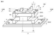
- the insulating support member 4 includes a third support portion 43, a fourth support portion 44, and a fifth support portion 45.
- the third support portion 43, the fourth support portion 44 and the fifth support portion 45 include a plurality of spacers.
- the third supporting portion 43, the fourth supporting portion 44 and the fifth supporting portion 45 are the same as each of the plurality of spacers.
- the third supporting portion 43 supports the circuit board 1 on the third insulating portion 23 .
- One end of the third support portion 43 is fixed to the circuit board 1 by each of the plurality of sixth fixtures F6.
- the other end of the third support portion 43 is fixed to the first insulating portion 21 by each of the plurality of seventh fixtures F7.
- the fourth support portion 44 supports the third insulating portion 23 on the fourth insulating portion 24 .
- One end of the fourth support portion 44 is fixed to the third insulating portion 23 by each of the plurality of eighth fixtures F8.
- the other end of the fourth support portion 44 is fixed to the fourth insulating portion 24 by each of the plurality of ninth fixtures F9.
- the fifth support portion 45 supports the fourth insulating portion 24 on the fifth insulating portion 25 .
- the fifth support portion 45 is fixed to the fourth insulating portion 24 by each of the plurality of tenth fixtures F10.
- the plurality of sixth fixtures F6, the plurality of seventh fixtures F7, the plurality of eighth fixtures F8, the plurality of ninth fixtures F9, and the plurality of tenth fixtures F10 are conductive.
- Each of the plurality of sixth fixtures F6, the plurality of seventh fixtures F7, the plurality of eighth fixtures F8, the plurality of ninth fixtures F9, and the plurality of tenth fixtures F10 is configured by, for example, a screw.
- the second surface 1 b of the circuit board 1 is spaced apart from the third insulating portion 23 by the third supporting portion 43 .
- the entire second surface 1 b of the circuit board 1 is spaced apart from the third insulating portion 23 by the third supporting portion 43 .
- the third insulating portion 23 is not in contact with the circuit board 1 .
- the third insulating portion 23 is spaced apart from the circuit board 1 in the direction from the first surface 1a to the second surface 1b.
- the third supporting portion 43 is exposed from the circuit board 1 and the third insulating portion 23 over the entire circumference.
- the third insulating portion 23 is spaced apart from the fourth insulating portion 24 by the fourth support portion 44 .
- the third insulating portion 23 is not in contact with the fourth insulating portion 24 .
- the third insulating portion 23 is spaced apart from the fourth insulating portion 24 in the direction from the first surface 1a toward the second surface 1b.
- the fourth support portion 44 is exposed from the third insulating portion 23 and the fourth insulating portion 24 over the entire circumference.
- the fourth insulating portion 24 is spaced apart from the fifth insulating portion 25 by the fifth support portion 45 .
- the fourth insulating portion 24 is not in contact with the fifth insulating portion 25 .
- the fourth insulating portion 24 is spaced apart from the fifth insulating portion 25 in the direction from the first surface 1a toward the second surface 1b.
- the fifth support portion 45 has portions exposed from the fourth insulating portion 24 and the fifth insulating portion 25 over the entire circumference.
- the fourth insulating portion 24 includes the third insulating portion 23 and the fifth insulating portion It is arranged inside the portion 25 .
- the fourth insulating portion 24 is not arranged on the same imaginary straight line extending in the thickness direction with respect to the third insulating portion 23 or the fifth insulating portion 25 .
- the third insulating portion 23 and the fifth insulating portion 25 may be arranged on the same imaginary straight line extending in the thickness direction.
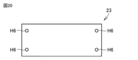
- the third insulating portion 23 is provided with a plurality of sixth penetrating portions H6 and a plurality of seventh penetrating portions H7.
- a third support portion 43 (see FIG. 13) is fixed to each of the plurality of sixth through portions H6 by a plurality of seventh fixtures F7 (see FIG. 13).
- a fourth support portion 44 (see FIG. 13) is fixed to each of the plurality of seventh penetrating portions H7 by each of a plurality of eighth fixtures F8 (see FIG. 13).
- the plurality of seventh penetrating portions H7 are arranged inside the plurality of sixth penetrating portions H6.
- Each of the plurality of seventh penetrating portions H7 is provided at the four corners of the third insulating portion 23 away from each of the plurality of sixth penetrating portions H6. Desirably, the shortest distance along the surface of the third insulating portion 23 from each seventh penetrating portion H7 to the sixth penetrating portion H6 arranged in the immediate vicinity of the seventh penetrating portion H7 is and each of the plurality of seventh penetrating portions H7.
- the fourth insulating portion 24 is provided with a plurality of eighth penetrating portions H8 and a plurality of ninth penetrating portions H9.
- a fourth support portion 44 (see FIG. 13) is fixed to each of the plurality of eighth penetrating portions H8 by a plurality of ninth fixtures F9 (see FIG. 13).
- a fifth support portion 45 (see FIG. 13) is fixed to each of the plurality of ninth penetrating portions H9 by each of a plurality of tenth fixtures F10 (see FIG. 13).
- the plurality of eighth penetrating portions H8 are arranged inside the plurality of ninth penetrating portions H9.
- Each of the plurality of ninth penetrating portions H9 is provided at the four corners of the fourth insulating portion 24 apart from each of the plurality of eighth penetrating portions H8. Desirably, the shortest distance along the surface of the fourth insulating portion 24 from each ninth penetrating portion H9 to the eighth penetrating portion H8 arranged in the immediate vicinity of the ninth penetrating portion H9 is and each of the plurality of ninth penetrating portions H9.
- the fifth insulating portion 25 is provided with a plurality of fourth engaging portions E4 and a plurality of tenth penetrating portions H10.
- the multiple fourth engaging portions E4 do not penetrate the fifth insulating portion 25 .
- the plurality of fourth engaging portions E4 are configured as screw holes, for example.
- a fifth support portion 45 (see FIG. 13) is fixed to each of the plurality of fourth engagement portions E4.
- the plurality of tenth penetrating portions H10 are provided at the four corners of the fifth insulating portion 25, respectively.
- the plurality of fourth engaging portions E4 are arranged inside the plurality of tenth penetrating portions H10.
- Each of the plurality of tenth penetrating portions H10 is provided at the four corners of the fifth insulating portion 25 away from each of the plurality of fourth engaging portions E4. Desirably, the shortest distance along the surface of the fifth insulating portion 25 from each tenth penetrating portion H10 to the fourth engaging portion E4 arranged in the immediate vicinity of the tenth penetrating portion H10 is a plurality of fourth engaging portions H10. The same is true for the portion E4 and each of the tenth penetrating portions H10.
- the creepage distance is the shortest distance f3 along the first surface 1a of the circuit board 1 between the conductive member 12 of the circuit board 1 and the sixth fixture F6,
- the creepage distance (f3+a3+b3+c3+d3+e3+f3+g3) of the present embodiment is from the conductive member 12 of the circuit board 1 to the third supporting portion 43, the third insulating portion 23, the fourth supporting portion 44, the fourth insulating portion 24, the fifth supporting portion 45 and It is the shortest creepage distance to the housing 3 via the fifth insulating portion 25 .
- the creepage distance (f3+a3+b3+c3+d3+e3+f3+g3) is designed to satisfy the creepage distance required by the standard.
- the spatial distance h3 is the sum of the shortest distance between the fixing portion 5 and the sixth fixture F6 and the shortest distance between the sixth fixture F6 and the conductive member 12 of the circuit board 1.
- the creepage distance (f3+a3+b3+c3+d3+e3+f3+g3) is longer than the clearance h3.
- the insulation performance (withstand voltage value) of the electronic device 100 increases as the creepage distance (f3+a3+b3+c3+d3+e3+f3+g3) increases.
- the in-plane dimension of the insulating plate 2 increases, the shortest distance g3 along the surface of the fifth insulating portion 25 between the fourth engaging portion E4 and the fixing portion 5 increases, so the creepage distance (f3+a3+b3+c3+d3+e3+f3+g3) increases Become. Therefore, as the in-plane dimension of the insulating plate 2 increases, the insulating performance (withstand voltage value) of the electronic device 100 improves. Also, the extra length difference between the creepage distance and the clearance distance is reduced.
- the creepage distance required for insulation between the circuit board 1 and the housing 3 is longer than the spatial distance required for insulation between the circuit board 1 and the housing 3 .
- the spatial distance required for insulation between the circuit board 1 and the housing 3 is h3, and the creepage distance required for insulation between the circuit board 1 and the housing 3 is (1.5 ⁇ h3).
- the creepage distance (f3+a3+b3+c3+d3+e3+f3+g3) is (1.5 ⁇ h3) or more, the circuit board 1 and the housing 3 are insulated.
- the creepage distance and the clearance are increased without increasing the dimension in the thickness direction of the electronic device 100 . That is, an increase in the thickness dimension of the electronic device 100 is suppressed while ensuring both the creepage distance and the clearance between the circuit board 1 and the housing 3 and the insulation performance.
- third insulating portion 23, fourth insulating portion 24, and fifth insulating portion 25 have an insulator structure. there is Therefore, the shortest distance a3 between the circuit board 1 and the third insulating portion 23 along the surface of the third insulating portion 23, and the distance between the third insulating portion 23 and the fourth insulating portion 24 along the surface of the fourth support portion 44 The shortest distance c3 and the shortest distance e3 between the fourth insulating portion 24 and the fifth insulating portion 25 along the surface of the fifth support portion 45 are increased.
- the creepage distance (f3+a3+b3+c3+d3+e3+f3+g3) can be increased without increasing the dimension of the electronic device 100 in the thickness direction. Also, the extra length difference between the creepage distance and the clearance distance is reduced.
- third insulating portion 23, fourth insulating portion 24, and fourth support portion 44 are integrally configured. there is The third insulating portion 23, the fourth insulating portion 24 and the fourth support portion 44 are not separated. The third insulating portion 23, the fourth insulating portion 24 and the fourth support portion 44 are joined together. As shown in FIG. 19, the third insulating portion 23, the fourth insulating portion 24 and the fourth insulating portion 24 are made of the same material. The third insulating portion 23, the fourth insulating portion 24, and the fourth insulating portion 24 are formed continuously. As shown in FIG.
- the third insulating portion 23 is provided with a plurality of sixth penetrating portions H6, but is not provided with a seventh penetrating portion H7 (see FIG. 14).
- the fourth insulating portion 24 is provided with a plurality of ninth penetrating portions H9, but is not provided with a plurality of eighth penetrating portions H8 (see FIG. 15).
- third insulating portion 23, fourth insulating portion 24, fifth insulating portion 25, third supporting portion 43, third The 4th support part 44 and the 5th support part 45 are integrally formed.
- the third insulating portion 23, the fourth insulating portion 24, the fifth insulating portion 25, the third supporting portion 43, the fourth supporting portion 44 and the fifth supporting portion 45 are not separated.
- the third insulating portion 23, the fourth insulating portion 24, the fifth insulating portion 25, the third supporting portion 43, the fourth supporting portion 44 and the fifth supporting portion 45 are joined. As shown in FIG.
- the third insulating portion 23, the fourth insulating portion 24, the fifth insulating portion 25, the third supporting portion 43, the fourth supporting portion 44 and the fifth supporting portion 45 are made of the same material. ing.
- the third insulating portion 23, the fourth insulating portion 24, the fifth insulating portion 25, the third supporting portion 43, the fourth supporting portion 44 and the fifth supporting portion 45 are formed continuously.
- the third insulating portion 23, the fourth insulating portion 24, the fifth insulating portion 25, the third supporting portion 43, the fourth supporting portion 44 and the fifth supporting portion 45 have the same width.
- the fifth insulating portion 25 is provided with a plurality of tenth through portions H10
- the third support portion 43 is provided with a plurality of eleventh through portions H11.
- a plurality of sixth fixtures F6 are fixed to each of the plurality of eleventh penetrating portions H11.
- the second surface 1b of the circuit board 1 is spaced apart from the third insulating portion 23 by the third supporting portion 43.
- the third insulating portion 23 is spaced from the fourth insulating portion 24 by the fourth support portion 44
- the fourth insulating portion 24 is spaced from the fifth insulating portion 25 by the fifth support portion 45 . are spaced apart. Therefore, the creepage distance and the spatial distance between the circuit board 1 and the housing 3 can be further increased. Therefore, the withstand voltage value of the electronic device 100 can be further increased. Since the creepage distance can be further increased, it is possible to further suppress the increase in the dimension of the electronic device 100 in the in-plane direction.
- the fourth supporting portion 44 As shown in FIG. 13, looking at the third supporting portion 43, the fourth supporting portion 44, and the fifth supporting portion 45 from the direction from the first surface 1a to the second surface 1b, the fourth supporting portion 44 It is arranged inside the third support portion 43 and the fifth support portion 45 . Therefore, the natural frequency of electronic device 100 is higher than in the case where third support portion 43, fourth support portion 44, and fifth support portion 45 are arranged on the same imaginary straight line extending in the thickness direction. can do. Therefore, the vibration resistance of the electronic device 100 can be improved.
- third support portion 43, fourth support portion 44, and fifth support portion 45 have an insulator structure. are doing. Therefore, the creepage distance can be further increased. Therefore, the withstand voltage value of the electronic device 100 can be further increased. Also, the electronic device 100 can have a double insulator structure.
- third insulating portion 23, fourth insulating portion 24, and fourth support portion 44 are integrally configured. It is Therefore, the rigidity of the electronic device 100 can be improved more than when the fourth insulating portion 24, the fourth insulating portion 24, and the fourth supporting portion 44 are separate members. Therefore, since the natural frequency of the electronic device 100 can be increased, the vibration resistance of the electronic device 100 can be improved. Further, by lengthening the fourth support portion 44, the third support portion 43 and the fifth support portion 45 can be shortened.
- the fourth support portion 44 and the fifth support portion 45 are integrally formed. Therefore, the rigidity of electronic device 100 can be further improved. Therefore, since the natural frequency of the electronic device 100 can be further increased, the vibration resistance of the electronic device 100 can be further improved.
- Embodiment 4 Next, the configuration of electronic device 100 according to Embodiment 4 will be described with reference to FIGS. 26 to 28.
- FIG. The fourth embodiment has the same configuration and effects as those of the first embodiment unless otherwise specified. Therefore, the same reference numerals are given to the same configurations as in the above-described first embodiment, and description thereof will not be repeated.
- insulating plate 2 of electronic device 100 includes grooves G.
- the insulating plate 2 has a first insulating surface 2a (upper surface), a second insulating surface 2b (lower surface), and an end surface 2c.
- the first insulating surface 2 a is a surface facing the second surface 1 b of the substrate portion 11 .
- the second insulating surface 2b is the surface opposite to the first insulating surface 2a.
- the end surface 2c is a side surface of the insulating plate 2. As shown in FIG. That is, the end surface 2c is a surface connecting the first insulating surface 2a and the second insulating surface 2b to each other.
- a plurality of grooves G are formed between the insulating support member 4 and the fixing portion 5 on the first insulating surface 2a.
- Groove G is formed to extend in a direction perpendicular to the cross section shown in FIG. In this way, the creepage distance is increased, so the insulation is improved without increasing the size of the electronic device 100 .
- the extending direction of the groove G may be any direction that intersects the direction from the insulating support member 4 toward the fixing portion 5 closest to the insulating support member 4 on the first insulating surface 2a.
- the groove G is formed on the first insulating surface 2a in the direction from the first insulating surface 2a toward the second insulating surface 2b. It is U-shaped.
- the cross-sectional shape of the groove G may be rectangular or V-shaped.
- the depth of the groove G is the distance in the thickness direction of the insulating plate 2 from the first insulating surface 2a to the bottom of the groove G in the cross-sectional view of the electronic device 100 shown in FIG.
- the bottom of the groove G is the point in the groove G that is farthest from the first insulating surface 2a in the thickness direction.
- the groove G is formed between the insulating support member 4 and the fixing portion 5, and the shape of the opening of the groove G on the first insulating surface 2a can be changed as appropriate.
- the width of the opening of the groove G in the X direction of FIG. 28 and the length of the opening of the groove G in the Y direction of FIG. 28 can be changed as appropriate.
- the length of the groove G may be longer than the distance from one of the two first through portions H1 adjacent to the groove G to the other first through portion H1. good.
- the length of the groove G may be longer than the distance from one of the two first engaging portions E1 adjacent to the groove G to the other first engaging portion E1.
- three grooves G are formed between the insulating support member 4 and the fixing portion 5, but the number may be one, two or four or more. Since the creepage distance increases, the number of grooves G formed is preferably as large as possible.
- the creepage distance is the shortest distance f4 along the first surface 1a of the circuit board 1 between the conductive member 12 of the circuit board 1 and the first fixture F1, and the insulation between the circuit board 1 and the insulating plate 2. It is the sum of the shortest distance a4 along the surface of the support member 4 and the shortest distance g4 between the first engaging portion E1 and the fixing portion 5 along the surface of the insulating plate 2 (f4+a4+g4). Note that the shortest distance g4 along the surface of the insulating plate 2 between the first engaging portion E1 and the fixing portion 5 is equal to the shortest distance in the first embodiment because the groove G is provided on the first insulating surface 2a. longer than g1.
- the creepage distance (f4+a4+g4) in this embodiment is the shortest creepage distance from the conductive member 12 of the circuit board 1 to the fixed portion 5 via the insulating support member 4 and the insulating plate 2.
- FIG. The creepage distance (f4+a4+g4) is designed to satisfy the creepage distance required by the standard.
- the spatial distance h4 is the sum of the shortest distance between the fixing portion 5 and the first fixture F1 and the shortest distance between the first fixture F1 and the conductive member 12 of the circuit board 1.
- the creepage distance (f4+a4+g4) is longer than the clearance h4.
- the insulation performance (withstand voltage value) of the electronic device 100 increases as the creepage distance (f4+a4+g4) increases. Therefore, the greater the number of grooves G formed between the insulating support member 4 and the fixing portion 5, the shorter the shortest distance g4 between the first engaging portion E1 and the fixing portion 5 along the surface of the insulating plate 2. become longer. Therefore, as the number of grooves G increases, the insulation performance (withstand voltage value) of the electronic device 100 improves.
- the creepage distance required for insulation between the circuit board 1 and the housing 3 is longer than the spatial distance required for insulation between the circuit board 1 and the housing 3 .
- the spatial distance required for insulation between the circuit board 1 and the housing 3 is h4, and the creepage distance required for insulation between the circuit board 1 and the housing 3 is (1.5 ⁇ h4).
- the creepage distance (f4+a4+g4) is (1.5 ⁇ h4) or more, the circuit board 1 and the housing 3 are insulated.
- the number of grooves G formed on the first insulating surface 2a is large, the dimension of the electronic device 100 in the thickness direction and the dimension of the insulating plate 2 in the plane along the first insulating surface 2a are increased. creepage distances and clearance distances are increased. That is, expansion of the thickness dimension and the in-plane dimension of the electronic device 100 is suppressed while ensuring both the creepage distance and the clearance distance between the circuit board 1 and the housing 3 and the insulation performance.
- the insulating support member 4 may have an insulator structure.
- the shortest distance a4 along the surface of the insulating support member 4 between the circuit board 1 and the insulating plate 2 is increased. Therefore, the creepage distance (f4+a4+g4) can be increased without increasing the dimension of the electronic device 100 in the thickness direction. Therefore, under the condition that the creepage distance is required to be longer than the spatial distance, it is possible to prevent the electronic device 100 from becoming excessively large in order to ensure the required insulation performance (creepage distance).
- insulating plate 2 has first insulating surface 2a.
- the first insulating surface 2a faces the second surface 1b.
- a groove G is formed between the insulating support member 4 and the fixed portion 5 in the first insulating surface 2a. Therefore, the creepage distance between the circuit board 1 and the housing 3 can be further increased. Therefore, the withstand voltage value of the electronic device 100 can be further increased. Since the creepage distance can be further increased, it is possible to further suppress the increase in the dimension of the electronic device 100 in the in-plane direction.
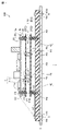
- Embodiment 5 Next, the configuration of electronic device 100 according to Embodiment 5 will be described with reference to FIGS. 29 to 34.
- FIG. The fifth embodiment has the same configuration and effects as those of the first embodiment unless otherwise specified. Therefore, the same reference numerals are given to the same configurations as in the above-described first embodiment, and description thereof will not be repeated.
- the fixing portion 5 is arranged so as to connect the housing 3 and the end surface 2c of the insulating plate 2 .
- first through portion H1 shown in FIG. 2 is not formed in insulating plate 2 .
- the fixing part 5 is composed of a fixture 5a and a fixture 5b.
- the shape of the fixture 5a is L-shaped.
- the fixture 5a has a first fixing portion 5a1 and a second fixing portion 5a2.
- the first fixing portion 5a1 is connected perpendicularly to the surface of the second fixing portion 5a2.
- a through hole 5ah is formed in each of the first fixing portion 5a1 and the second fixing portion 5a2.
- a plurality of horizontal holes 2h are formed in the end surface 2c of the insulating plate 2 in a side view of the insulating plate 2 viewed from the X direction in FIG.
- a plurality of through holes TH are formed outside the outer periphery of the insulating plate 2 when the housing 3 is viewed from the thickness direction of the housing 3 .
- Fixtures 5b are respectively inserted into the horizontal hole 2h and the through hole TH. In other words, the fixture 5b is inserted into the through hole 5ah and the horizontal hole 2h formed in the first fixing portion 5a1 so that the first fixing portion 5a1 is fixed to the end surface 2c, thereby connecting the first fixing portion 5a1 and the end surface 2c.
- the fixture 5b is inserted into the through hole 5ah and the through hole TH formed in the second fixing portion 5a2 so that the second fixing portion 5a2 is fixed to the housing 3, and the second fixing portion 5a2 and the housing are connected. to conclude.
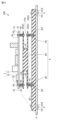
- the creepage distance and the clearance distance are increased, so that the insulation performance is improved without increasing the size of the electronic device 100 .
- the number of fixtures 5a and fixtures 5b may be one or more.
- the through holes TH and the horizontal holes 2h may be formed such that the numbers of the through holes TH and the horizontal holes 2h match the numbers of the fixtures 5a.
- the through hole TH and the horizontal hole 2h are arranged so that the fixture 5a is connected to the side surface (end surface 2c) of the housing 3 and the insulating plate 2, respectively.
- the material of the fixture 5a may be, for example, a steel material such as steel or ferrous alloy.
- the material of the fixture 5a may be, for example, metals such as aluminum (Al) and copper (Cu), and non-ferrous metals such as alloys containing these.
- the material of the fixture 5a may be resin.
- the fixture 5b is configured by, for example, a screw.
- the screws are pan screws, for example, and are made of metal such as aluminum (Al), iron (Fe), stainless steel, and brass.
- the fixture 5b has conductivity.
- the fixture 5a does not have to connect the end surface 2c and the housing 3 using the fixture 5b.
- the fixture 5a, the end surface 2c and the housing 3 may be joined by welding.
- the creepage distance is the shortest distance f5 along the first surface 1a of the circuit board 1 between the conductive member 12 of the circuit board 1 and the first fixture F1, and the insulation between the circuit board 1 and the insulating plate 2. It is the sum of the shortest distance a5 along the surface of the support member 4 and the shortest distance g5 between the first engaging portion E1 and the fixing portion 5 along the surface of the insulating plate 2 (f5+a5+g5). Note that the shortest distance g5 between the first engaging portion E1 and the fixed portion 5 along the surface of the insulating plate 2 is the shortest distance g5 in the first embodiment because the fixed portion 5 is arranged on the end face 2c of the insulating plate 2. longer than the distance g1.
- the creepage distance (f5+a5+g5) of the present embodiment is the shortest creepage distance from the conductive member 12 of the circuit board 1 to the fixed portion 5 via the insulating support member 4 and the insulating plate 2.
- FIG. The creepage distance (f5+a5+g5) is designed to satisfy the creepage distance required by the standard.
- the spatial distance h5 is the sum of the shortest distance between the fixing portion 5 and the first fixture F1 and the shortest distance between the first fixture F1 and the conductive member 12 of the circuit board 1.
- the spatial distance h5 is longer than the spatial distance h5 in the first embodiment because the fixing portion 5 is arranged on the end surface 2c of the insulating plate 2. As shown in FIG.
- the creepage distance (f5+a5+g5) is longer than the clearance h5.
- the insulation performance (withstanding voltage value) of the electronic device 100 increases as the creepage distance (f5+a5+g5) increases. Therefore, the larger the in-plane dimension of the insulating plate 2, the longer the shortest distance g5 along the surface of the insulating plate 2 between the first engaging portion E1 and the fixing portion 5, so that the creeping distance (f5+a5+g5) becomes longer. Become. Therefore, as the in-plane dimension of the insulating plate 2 increases, the insulating performance (withstand voltage value) of the electronic device 100 improves.
- the creepage distance required for insulation between the circuit board 1 and the housing 3 is longer than the spatial distance required for insulation between the circuit board 1 and the housing 3 .
- the spatial distance required for insulation between the circuit board 1 and the housing 3 is h5
- the creepage distance required for insulation between the circuit board 1 and the housing 3 is (1.5 ⁇ h5).
- the creepage distance (f5+a5+g5) is (1.5 ⁇ h5) or more
- the circuit board 1 and the housing 3 are insulated.
- the fixture 5b is arranged on the end surface 2c, the creepage distance and the spatial distance are increased without increasing the size of the electronic device 100 in the thickness direction as compared with the first embodiment. That is, expansion of the thickness dimension and the in-plane dimension of the electronic device 100 is suppressed while ensuring both the creepage distance and the clearance distance between the circuit board 1 and the housing 3 and the insulation performance.
- the insulating support member 4 may have an insulator structure.
- the shortest distance a5 along the surface of the insulating support member 4 between the circuit board 1 and the insulating plate 2 is increased. Therefore, the creepage distance (f5+a5+g5) can be increased without increasing the dimension of the electronic device 100 in the thickness direction. Therefore, under the condition that the creepage distance is required to be longer than the spatial distance, it is possible to prevent the electronic device 100 from becoming excessively large in order to ensure the required insulation performance (creepage distance).
- insulating plate 2 has first insulating surface 2a and end surface 2c.
- the end surface 2c continues to the first insulating surface 2a.
- the fixing portion 5 connects the housing 3 and the end face 2c. Therefore, the creepage distance between the circuit board 1 and the fixing portion 5 can be further increased. Therefore, the withstand voltage value of the electronic device 100 can be further increased. Since the creepage distance and the spatial distance can be further increased, it is possible to further suppress the increase in the in-plane dimension of electronic device 100 .
- fixing portion 5 has first fixing portion 5a1 and second fixing portion 5a2.
- the first fixing portion 5a1 and the second fixing portion 5a2 are connected to each other.
- the first fixing portion 5a1 is fixed to the end surface 2c.
- the second fixing portion 5 a 2 is fixed to the housing 3 . Therefore, if the through holes 5ah are formed in the first fixing portion 5a1 and the second fixing portion 5a2, the housing 3 and the end surface 2c can be mechanically fastened using the fixture 5b.
Landscapes
- Engineering & Computer Science (AREA)
- Microelectronics & Electronic Packaging (AREA)
- Power Engineering (AREA)
- Physics & Mathematics (AREA)
- Condensed Matter Physics & Semiconductors (AREA)
- General Physics & Mathematics (AREA)
- Computer Hardware Design (AREA)
- Mounting Of Printed Circuit Boards And The Like (AREA)
Abstract
Provided is an electronic device in which the occurrence of dielectric breakdown is suppressed. The electronic device (100) comprises a circuit substrate (1), an insulating plate (2), a housing (3), and an insulated support material (4). The circuit substrate (1) includes an electrically conductive member (12), a first surface (1a), and a second surface (1b). The electrically conductive member (12) is disposed on the first surface (1a). The second surface (1b) is opposite the first surface (1a). The insulating plate (2) is disposed on a side opposite to the first surface (1a) with respect to the second surface (1b). The housing (3) has electrical conductivity. The housing (3) is in contact with the insulating plate (2) on a side opposite to the circuit substrate (1) with respect to the insulating plate (2). The insulated support material (4) supports the circuit substrate (1) on the insulating plate (2). The insulated support material (4) is electrically insulated from the housing (3). The second surface (1b) of the circuit substrate (1) is spaced apart from the insulating plate (2) due to the insulated support material (4).
Description
本開示は、電子機器に関するものである。
This disclosure relates to electronic equipment.
従来、プリント基板(回路基板)と、絶縁板と、金属筐体(筐体)とを含む電子機器がある。例えば、特許第6620506号公報(特許文献1)に記載の電子機器のプリント基板絶縁構造では、絶縁板は、プリント基板と金属筐体との間に配置されている。
Conventionally, there are electronic devices that include a printed board (circuit board), an insulating plate, and a metal housing (housing). For example, in a printed circuit board insulation structure for an electronic device disclosed in Japanese Patent No. 6620506 (Patent Document 1), an insulating plate is arranged between the printed circuit board and a metal housing.
上記文献に記載の電子機器では、絶縁板がプリント基板および金属筐体に接触することによってプリント基板と金属筐体との絶縁が確保されている。しかしながら、絶縁板の表面には凹凸が設けられていることがあるため、絶縁板をプリント基板に隙間無く接触させることは難しい。絶縁板の表面の凹凸によって、絶縁板とプリント基板との間にボイド、空隙等の欠陥が介在することがある。絶縁板の表面に汚れ等が付着している場合には、沿面放電の開始電圧が低下する。沿面放電の開始電圧よりも高い電圧が印加された場合には、上記のボイド、空隙等の欠陥が放電の基点となって沿面放電が発生し、最終的に絶縁破壊に至ることがある。
In the electronic device described in the above document, insulation between the printed circuit board and the metal casing is ensured by the contact of the insulating plate with the printed circuit board and the metal casing. However, since the surface of the insulating plate may have irregularities, it is difficult to bring the insulating plate into contact with the printed circuit board without gaps. Defects such as voids and gaps may intervene between the insulating plate and the printed circuit board due to unevenness on the surface of the insulating plate. If dirt or the like adheres to the surface of the insulating plate, the creeping discharge initiation voltage is lowered. When a voltage higher than the start voltage of the creeping discharge is applied, defects such as the voids and gaps become the starting point of the discharge, causing the creeping discharge, which may eventually lead to dielectric breakdown.
本開示は上記課題に鑑みてなされたものであり、その目的は、絶縁破壊が生じることを抑制することができる電子機器を提供することである。
The present disclosure has been made in view of the above problems, and an object thereof is to provide an electronic device capable of suppressing the occurrence of dielectric breakdown.
本開示の電子機器は、回路基板と、絶縁板と、筐体と、絶縁支持材とを備えている。回路基板は、導電部材と、第1面と、第2面とを含んでいる。第1面には、導電部材が配置されている。第2面は、第1面に対向している。絶縁板は、第2面に対して第1面とは反対側に配置されている。筐体は、導電性を有している。筐体は、絶縁板に対して回路基板とは反対側において絶縁板に接触している。絶縁支持材は、回路基板を絶縁板に支持している。絶縁支持材は、筐体に対して電気的に絶縁されている。回路基板の第2面は、絶縁支持材によって絶縁板から間隔を空けて配置されている。
The electronic device of the present disclosure includes a circuit board, an insulating plate, a housing, and an insulating support. The circuit board includes a conductive member, a first side and a second side. A conductive member is arranged on the first surface. The second surface faces the first surface. The insulating plate is arranged on the side opposite to the first surface with respect to the second surface. The housing has electrical conductivity. The housing is in contact with the insulating plate on the side opposite to the circuit board with respect to the insulating plate. An insulating support supports the circuit board to the insulating plate. The insulating support is electrically insulated with respect to the housing. The second side of the circuit board is spaced from the insulating plate by an insulating support.
本開示の電子機器によれば、回路基板の第2面は、絶縁支持材によって絶縁板から間隔を空けて配置されている。このため、絶縁板のボイド、空隙等の欠陥を基点とした沿面放電が発生することを抑制することができる。よって、絶縁破壊が生じることを抑制することができる。
According to the electronic device of the present disclosure, the second surface of the circuit board is spaced apart from the insulating plate by the insulating support member. Therefore, it is possible to suppress the occurrence of creeping discharge originating from defects such as voids and gaps in the insulating plate. Therefore, it is possible to suppress the occurrence of dielectric breakdown.
以下、実施の形態について図に基づいて説明する。なお、以下では、同一または相当する部分に同一の符号を付すものとし、重複する説明は繰り返さない。
Embodiments will be described below based on the drawings. In addition, below, the same code|symbol shall be attached|subjected to the same or corresponding part, and the overlapping description is not repeated.
実施の形態1.
図1~図5を用いて、実施の形態1に係る電子機器100の構成を説明する。Embodiment 1.
The configuration ofelectronic device 100 according to the first embodiment will be described with reference to FIGS. 1 to 5. FIG.
図1~図5を用いて、実施の形態1に係る電子機器100の構成を説明する。
The configuration of
図1に示されるように、電子機器100は、例えば、制御機器である。電子機器100は、主に、回路基板1と、絶縁板2と、筐体3と、絶縁支持材4と、固定部5とを含んでいる。なお、以下の説明においては、厚さ方向と、面内方向とを用いて電子機器100の構成を説明する。厚さ方向は、面内方向に交差している。本実施の形態では、厚さ方向は、面内方向に直交している。
As shown in FIG. 1, electronic device 100 is, for example, a control device. Electronic device 100 mainly includes circuit board 1 , insulating plate 2 , housing 3 , insulating support member 4 , and fixing portion 5 . In the following description, the configuration of electronic device 100 will be described using the thickness direction and the in-plane direction. The thickness direction crosses the in-plane direction. In this embodiment, the thickness direction is orthogonal to the in-plane direction.
図1に示されるように、回路基板1は、基板部11と、導電部材12とを含んでいる。基板部11は、第1面1aと、第2面1bとを含んでいる。基板部11には、導電部材12が搭載されている。導電部材12は、導電性を有している。導電部材12は、例えば、電子部品、電気部品、金属配線パターン等である。基板部11は、平板形状を有している。第1面1aには、導電部材12が配置されている。第2面1bは、第1面1aに対向している。望ましくは、第2面1bには、導電部材12が配置されていない。第2面1bは、厚さ方向に沿って第1面1aに対向している。回路基板1は、面内方向に沿って延在している。基板部11は、例えば、紙フェノール、ガラスエポキシ樹脂等のプリント基板用部材によって構成されている。基板部11の厚みは、例えば、0.4mm以上3.2mm以下である。基板部11の幅および長さは、例えば、25mm以上550mm以下である。
As shown in FIG. 1, the circuit board 1 includes a board portion 11 and a conductive member 12. As shown in FIG. The substrate portion 11 includes a first surface 1a and a second surface 1b. A conductive member 12 is mounted on the substrate portion 11 . The conductive member 12 has conductivity. The conductive member 12 is, for example, an electronic component, an electrical component, a metal wiring pattern, or the like. The substrate portion 11 has a flat plate shape. A conductive member 12 is arranged on the first surface 1a. The second surface 1b faces the first surface 1a. Desirably, the conductive member 12 is not arranged on the second surface 1b. The second surface 1b faces the first surface 1a along the thickness direction. The circuit board 1 extends along the in-plane direction. The board portion 11 is made of a printed board member such as paper phenol, glass epoxy resin, or the like. The thickness of the substrate portion 11 is, for example, 0.4 mm or more and 3.2 mm or less. The width and length of the substrate portion 11 are, for example, 25 mm or more and 550 mm or less.
絶縁板2は、第2面1bに対して第1面1aとは反対側に配置されている。絶縁板2は、絶縁性を有している。絶縁板2は、例えば、エポキシ樹脂等の絶縁性の樹脂によって構成されている。絶縁板2は、面内方向に沿って延在している。絶縁板2は、回路基板1よりも大きい面内方向の寸法を有している。
The insulating plate 2 is arranged on the side opposite to the first surface 1a with respect to the second surface 1b. The insulating plate 2 has insulating properties. The insulating plate 2 is made of, for example, insulating resin such as epoxy resin. The insulating plate 2 extends along the in-plane direction. The insulating plate 2 has an in-plane dimension larger than that of the circuit board 1 .
筐体3は、絶縁板2に対して回路基板1とは反対側において絶縁板2に接触している。筐体3は、絶縁板2から間隔を空けずに配置されている。筐体3は、絶縁板2に隙間なく接触していることが望ましい。筐体3には、絶縁板2が固定されている。筐体3は、絶縁板2よりも大きい面内方向の寸法を有している。筐体3は、導電性を有している。筐体3は、金属によって構成されている。筐体3は、例えば、スチール、含鉄合金を代表とした鉄鋼類によって構成されている。筐体3は、例えば、アルミニウム(Al)、銅(Cu)等の金属を含む合金等の非鉄金属によって構成されている。
The housing 3 is in contact with the insulating plate 2 on the side opposite to the circuit board 1 with respect to the insulating plate 2 . The housing 3 is arranged without leaving an interval from the insulating plate 2 . It is desirable that the housing 3 is in contact with the insulating plate 2 without gaps. An insulating plate 2 is fixed to the housing 3 . The housing 3 has an in-plane dimension larger than that of the insulating plate 2 . The housing 3 has conductivity. The housing 3 is made of metal. The housing 3 is made of, for example, iron and steel typified by steel and iron-containing alloys. The housing 3 is made of, for example, a non-ferrous metal such as an alloy containing a metal such as aluminum (Al) or copper (Cu).
絶縁支持材4は、回路基板1を絶縁板2に支持している。回路基板1と絶縁板2との間には、絶縁支持材4が介在している。絶縁支持材4は、全周にわたって回路基板1および絶縁板2から露出した部分を有している。絶縁支持材4の一方端は、複数の第1固定具F1の各々によって回路基板1に固定されている。本実施の形態において、絶縁支持材4は、複数のスペーサ40を含んでいる。絶縁支持材4は、例えば、4つのスペーサ40を含んでいる。複数のスペーサ40の各々は、回路基板1を絶縁板2に支持している。複数のスペーサ40の各々は、互いに同じ形状を有している。複数のスペーサ40の各々は、絶縁支持材4と同じものである。
The insulating support member 4 supports the circuit board 1 on the insulating plate 2 . An insulating support member 4 is interposed between the circuit board 1 and the insulating plate 2 . The insulating support member 4 has portions exposed from the circuit board 1 and the insulating plate 2 over the entire circumference. One end of insulating support member 4 is fixed to circuit board 1 by each of a plurality of first fixtures F1. In this embodiment, insulating support 4 includes a plurality of spacers 40 . The insulating support 4 contains, for example, four spacers 40 . Each of the plurality of spacers 40 supports the circuit board 1 on the insulating plate 2 . Each of the plurality of spacers 40 has the same shape as each other. Each of the plurality of spacers 40 is the same as the insulating support material 4 .
図2に示されるように、絶縁支持材4は、筐体3に対して電気的に絶縁されている。絶縁支持材4に支持された回路基板1も筐体3に対して電気的に絶縁されている。絶縁支持材4の他方端は、絶縁板2に埋め込まれている。絶縁支持材4の他方端は、絶縁板2を貫通していない。絶縁支持材4の他方端は、筐体3に接触していない。絶縁支持材4の他方端は、筐体3に対して電気的に絶縁されている。絶縁支持材4は、絶縁板2および筐体3とは別体として構成されている。
As shown in FIG. 2, the insulating support material 4 is electrically insulated from the housing 3. The circuit board 1 supported by the insulating support member 4 is also electrically insulated from the housing 3 . The other end of the insulating support member 4 is embedded in the insulating plate 2 . The other end of the insulating support member 4 does not penetrate the insulating plate 2 . The other end of the insulating support member 4 is not in contact with the housing 3 . The other end of the insulating support member 4 is electrically insulated from the housing 3 . The insulating support member 4 is configured separately from the insulating plate 2 and the housing 3 .
絶縁支持材4は、絶縁性を有している。絶縁支持材4は、例えば、ジュラコン(登録商標)、ナイロン等の絶縁性の材料によって構成されている。絶縁支持材4の形状は、例えば、直線状である。絶縁支持材4は、後述のように、碍子として構成されていてもよい。
The insulating support material 4 has insulating properties. The insulating support member 4 is made of an insulating material such as Duracon (registered trademark) or nylon. The shape of the insulating support member 4 is, for example, linear. The insulating support member 4 may be configured as an insulator as described below.
回路基板1の第2面1bは、絶縁支持材4によって絶縁板2から間隔を空けて配置されている。絶縁板2は、回路基板1の第2面1bと接触していない。回路基板1の第2面1bの全面は、絶縁支持材4によって絶縁板2から間隔を空けて配置されている。回路基板1と絶縁板2とは、絶縁支持材4のみを介して接続されている。
The second surface 1 b of the circuit board 1 is spaced apart from the insulating plate 2 by the insulating support material 4 . The insulating plate 2 is not in contact with the second surface 1 b of the circuit board 1 . The entire second surface 1 b of the circuit board 1 is spaced apart from the insulating plate 2 by the insulating support member 4 . The circuit board 1 and the insulating plate 2 are connected only through the insulating support member 4 .
固定部5は、絶縁板2を筐体3に固定している。固定部5は、絶縁板2を筐体3に機械的に締結することで絶縁板2を筐体3に固定している。固定部5は、例えば、複数のリベット50(図1参照)によって構成されている。固定部5がリベットである場合には、リベットが絶縁板2の第1貫通部H1および筐体3の下孔を貫通した状態でリベットがリベッター工具によって加工されることで、絶縁板2が筐体3に固定される。なお、固定部5は、例えば、複数のねじによって構成されていてもよい。固定部5がねじである場合には、筐体3に事前にナットがかしめ加工によって設けられており、ねじがナットに対してねじ止めされることで絶縁板2が筐体3に固定される。固定部5は、導電性を有している。固定部5は、例えば、アルミニウム(Al)、ステンレス等の金属によって構成されている。固定部5は、複数のリベットの各々または複数のねじの各々と同じものである。
The fixing part 5 fixes the insulating plate 2 to the housing 3 . The fixing portion 5 fixes the insulating plate 2 to the housing 3 by mechanically fastening the insulating plate 2 to the housing 3 . The fixing portion 5 is configured by, for example, a plurality of rivets 50 (see FIG. 1). In the case where the fixing portion 5 is a rivet, the rivet is processed by a riveter tool in a state in which the rivet penetrates the first through portion H1 of the insulating plate 2 and the pilot hole of the housing 3, thereby fixing the insulating plate 2 to the housing. It is fixed to the body 3. Note that the fixing portion 5 may be configured by, for example, a plurality of screws. When the fixing part 5 is a screw, the housing 3 is provided with a nut in advance by crimping, and the insulating plate 2 is fixed to the housing 3 by screwing the screw to the nut. . The fixed part 5 has conductivity. The fixed portion 5 is made of metal such as aluminum (Al) or stainless steel. The fixing part 5 is the same as each of the rivets or each of the screws.
第1面1aから第2面1bに向かう方向に沿って回路基板1および固定部5を見たときに、固定部5は、回路基板1よりも外側に配置されている。第1面1aから第2面1bに向かう方向に沿って固定部5を見たときに、固定部5は、回路基板1から露出している。固定部5から導電部材12までの沿面距離および空間距離は、導電部材12から絶縁板2までの沿面距離および空間距離よりも長い。
The fixing part 5 is arranged outside the circuit board 1 when the circuit board 1 and the fixing part 5 are viewed along the direction from the first surface 1a to the second surface 1b. The fixing portion 5 is exposed from the circuit board 1 when the fixing portion 5 is viewed along the direction from the first surface 1a to the second surface 1b. The creepage distance and the spatial distance from the fixed portion 5 to the conductive member 12 are longer than the creepage distance and the spatial distance from the conductive member 12 to the insulating plate 2 .
複数の第1固定具F1は、回路基板1を絶縁支持材4に固定している。複数の第1固定具F1は、回路基板1を絶縁支持材4に機械的に締結することで回路基板1を絶縁支持材4に固定している。複数の第1固定具F1は、基板部11を貫通した状態で絶縁支持材4に固定されている。複数の第1固定具F1の各々は、例えば、ねじによって構成されている。ねじは、例えば、ナベ小ねじであり、鉄(Fe)、ステンレス、真鍮等の金属によって構成されている。複数の第1固定具F1は、導電性を有している。
The plurality of first fixtures F1 fix the circuit board 1 to the insulating support member 4. The plurality of first fixtures F1 fix the circuit board 1 to the insulating support member 4 by mechanically fastening the circuit board 1 to the insulating support member 4 . A plurality of first fixtures F1 are fixed to the insulating support member 4 while passing through the substrate portion 11 . Each of the multiple first fixtures F1 is configured by, for example, a screw. The screw is, for example, a pan screw, and is made of metal such as iron (Fe), stainless steel, or brass. The multiple first fixtures F1 are conductive.
図3に示されるように、回路基板1には、複数の挿通孔IHが設けられている。複数の挿通孔IHの各々には、第1固定具F1(図2参照)が挿入される。複数の挿通孔IHは、雌ネジとして構成されている。回路基板1の四隅の各々には、複数の挿通孔IHの各々が設けられている。
As shown in FIG. 3, the circuit board 1 is provided with a plurality of insertion holes IH. A first fixture F1 (see FIG. 2) is inserted into each of the plurality of insertion holes IH. The plurality of insertion holes IH are configured as female threads. Each of the four corners of the circuit board 1 is provided with a plurality of insertion holes IH.
図4に示されるように、絶縁板2には、複数の第1貫通部H1および複数の第1係合部E1が設けられている。複数の第1貫通部H1の各々には、固定部5(図2参照)が挿入される。絶縁板2の四隅の各々には、複数の第1貫通部H1の各々が設けられている。複数の第1係合部E1は、絶縁板2を貫通していない。複数の第1係合部E1は、例えば、ネジ穴として構成されている。複数の第1係合部E1の各々には、絶縁支持材4(図2参照)が固定される。厚さ方向に沿って絶縁板2を見たときに、複数の第1貫通部H1は、複数の第1係合部E1よりも外側に配置されている。望ましくは、各第1貫通部H1からその第1貫通部H1の直近に配置された第1係合部E1までの絶縁板2の表面に沿った最短距離は、複数の第1貫通部H1および複数の第1係合部E1の各々において同じである。
As shown in FIG. 4, the insulating plate 2 is provided with a plurality of first penetrating portions H1 and a plurality of first engaging portions E1. A fixing portion 5 (see FIG. 2) is inserted into each of the plurality of first penetrating portions H1. Each of the four corners of the insulating plate 2 is provided with a plurality of first penetrating portions H1. The plurality of first engaging portions E1 do not penetrate the insulating plate 2 . The plurality of first engaging portions E1 are configured as screw holes, for example. An insulating support member 4 (see FIG. 2) is fixed to each of the plurality of first engaging portions E1. When the insulating plate 2 is viewed along the thickness direction, the plurality of first penetrating portions H1 are arranged outside the plurality of first engaging portions E1. Desirably, the shortest distance along the surface of the insulating plate 2 from each first penetrating portion H1 to the first engaging portion E1 arranged in the immediate vicinity of the first penetrating portion H1 is The same is true for each of the plurality of first engaging portions E1.
図5に示されるように、筐体3には、複数の貫通孔THが設けられている。複数の貫通孔THの各々には、固定部5(図2参照)が挿入される。筐体3の四隅の各々には、複数の貫通孔の各々が設けられている。
As shown in FIG. 5, the housing 3 is provided with a plurality of through holes TH. A fixing portion 5 (see FIG. 2) is inserted into each of the plurality of through holes TH. Each of the four corners of the housing 3 is provided with a plurality of through holes.
〈電子機器100の沿面距離および空間距離について〉
次に、図2を用いて、電子機器100の沿面距離および空間距離について説明する。 <Creepage Distance and Spatial Distance ofElectronic Device 100>
Next, creepage distances and spatial distances ofelectronic device 100 will be described with reference to FIG.
次に、図2を用いて、電子機器100の沿面距離および空間距離について説明する。 <Creepage Distance and Spatial Distance of
Next, creepage distances and spatial distances of
回路基板1と筐体3との絶縁のための絶縁距離には、沿面距離と、空間距離とがある。沿面距離は、回路基板1と筐体3との絶縁体を介した最短距離である。図2では、沿面距離は、実線による矢印によって示されている。空間距離は、回路基板1と筐体3との空気を介した最短距離である。図2では、空間距離は、破線による矢印によって示されている。
The insulation distance for insulation between the circuit board 1 and the housing 3 includes a creepage distance and a spatial distance. The creepage distance is the shortest distance between the circuit board 1 and the housing 3 via an insulator. In FIG. 2, the creepage distance is indicated by a solid arrow. The spatial distance is the shortest distance between the circuit board 1 and the housing 3 through the air. In FIG. 2, the spatial distances are indicated by dashed arrows.
本実施の形態において、沿面距離は、回路基板1の導電部材12(金属配線パターン)と第1固定具F1との回路基板1の第1面1aに沿った最短距離f1、回路基板1と絶縁板2との絶縁支持材4の表面に沿った最短距離a1および絶縁支持材4と固定部5との絶縁板2の表面に沿った最短距離g1の和(f1+a1+g1)である。なお、最短距離a1は、回路基板1と絶縁板2との間における絶縁支持材4の厚さ方向の寸法でもある。本実施の形態の沿面距離は、回路基板1の導電部材12から絶縁支持材4および絶縁板2を経由した固定部5までの最短の沿面距離である。本実施の形態の最短の沿面距離は、規格に要求された沿面距離を満足するように設計される。
In the present embodiment, the creepage distance is the shortest distance f1 along the first surface 1a of the circuit board 1 between the conductive member 12 (metal wiring pattern) of the circuit board 1 and the first fixture F1, It is the sum (f1+a1+g1) of the shortest distance a1 along the surface of the insulating support member 4 to the plate 2 and the shortest distance g1 along the surface of the insulating plate 2 between the insulating support member 4 and the fixed portion 5. The shortest distance a1 is also the dimension in the thickness direction of the insulating support member 4 between the circuit board 1 and the insulating plate 2. As shown in FIG. The creepage distance in the present embodiment is the shortest creepage distance from conductive member 12 of circuit board 1 to fixed portion 5 via insulating support member 4 and insulating plate 2 . The shortest creepage distance of this embodiment is designed to satisfy the creepage distance required by the standard.
電子機器100の絶縁性能(耐電圧値)は、沿面距離(f1+a1+g1)が長いほど高くなる。このため、絶縁板2の面内方向の寸法が大きくなるほど、絶縁支持材4と固定部5との絶縁板2の表面に沿った最短距離g1が長くなり、沿面距離(f1+a1+g1)が長くなる。よって、絶縁板2の面内方向の寸法が大きくなるほど、電子機器100の絶縁性能(耐電圧値)が大きくなる。
The insulation performance (withstand voltage value) of the electronic device 100 increases as the creepage distance (f1+a1+g1) increases. Therefore, the larger the in-plane dimension of the insulating plate 2, the longer the shortest distance g1 along the surface of the insulating plate 2 between the insulating support member 4 and the fixed portion 5, and the longer the creeping distance (f1+a1+g1). Therefore, the larger the dimension of the insulating plate 2 in the in-plane direction, the higher the insulating performance (withstand voltage value) of the electronic device 100 .
本実施の形態において、空間距離h1は、固定部5と第1固定具F1との最短距離および第1固定具F1と回路基板1の導電部材12との最短距離の和である。沿面距離(f1+a1+g1)は、空間距離h1よりも長い。
In the present embodiment, the spatial distance h1 is the sum of the shortest distance between the fixing portion 5 and the first fixture F1 and the shortest distance between the first fixture F1 and the conductive member 12 of the circuit board 1. The creepage distance (f1+a1+g1) is longer than the clearance h1.
回路基板1と筐体3との絶縁のために必要な空間距離よりも回路基板1と筐体3との絶縁のために必要な沿面距離の方が長い。例えば、回路基板1と筐体3との絶縁のために必要な空間距離がh1であり、回路基板1と筐体3との絶縁のために必要な沿面距離が(1.5×h1)である場合には、沿面距離(f1+a1+g1)が(1.5×h1)以上であれば回路基板1と筐体3とが絶縁される。また、絶縁板2の面内方向の寸法が拡大されることで、電子機器100の厚さ方向の寸法が拡大されることなく、沿面距離および空間距離が大きくされる。すなわち、回路基板1と筐体3との沿面距離および空間距離の確保と絶縁性能とを両立した状態で、電子機器100の厚さ方向の寸法の拡大が抑制される。
The creepage distance required for insulation between the circuit board 1 and the housing 3 is longer than the spatial distance required for insulation between the circuit board 1 and the housing 3 . For example, the spatial distance required for insulation between the circuit board 1 and the housing 3 is h1, and the creepage distance required for insulation between the circuit board 1 and the housing 3 is (1.5×h1). In some cases, the circuit board 1 and the housing 3 are insulated if the creepage distance (f1+a1+g1) is (1.5×h1) or more. Further, by increasing the dimension of the insulating plate 2 in the in-plane direction, the creepage distance and the clearance are increased without increasing the dimension in the thickness direction of the electronic device 100 . That is, the expansion of the dimension of the electronic device 100 in the thickness direction is suppressed while ensuring both the creepage distance and the clearance between the circuit board 1 and the housing 3 and the insulation performance.
図6に示されるように、絶縁支持材4は、碍子として構成されていてもよい。碍子として構成された絶縁支持材4は、軸部4aと、軸部4aから張り出した複数の張出部4bとを含んでいる。この場合には、絶縁支持材4の厚さ方向の寸法が維持されたままで、回路基板1と絶縁板2との絶縁支持材4の表面に沿った最短距離a1が大きくなる。これにより、電子機器100の絶縁性能(耐電圧値)が大きくなる。規格においては沿面距離が空間距離よりも長いことが求められるが、沿面距離が空間距離よりも過剰に長い場合には電子機器100が過剰に大型化する。すなわち、沿面距離と空間距離との間の余分な長さの差がある場合には、電子機器100が過剰に大型化する。沿面距離と空間距離との間の余分な長さの差は、碍子によって低減される。
As shown in Fig. 6, the insulating support material 4 may be configured as an insulator. The insulating support member 4 configured as an insulator includes a shaft portion 4a and a plurality of projecting portions 4b projecting from the shaft portion 4a. In this case, the shortest distance a1 between the circuit board 1 and the insulating plate 2 along the surface of the insulating support member 4 is increased while the thickness dimension of the insulating support member 4 is maintained. Thereby, the insulation performance (withstand voltage value) of the electronic device 100 is increased. The standard requires that the creepage distance be longer than the spatial distance, but if the creepage distance is excessively longer than the spatial distance, the electronic device 100 becomes excessively large. That is, if there is an extra length difference between the creepage distance and the spatial distance, the electronic device 100 becomes excessively large. The extra length difference between the creepage distance and the clearance distance is reduced by the insulator.
次に、図7に示される比較例に係る電子機器101と本実施の形態に係る電子機器100とを比較して、本実施の形態に係る電子機器100の作用効果を説明する。
Next, the effects of the electronic device 100 according to the present embodiment will be described by comparing the electronic device 101 according to the comparative example shown in FIG. 7 and the electronic device 100 according to the present embodiment.
図7に示されるように、比較例に係る電子機器101は、絶縁板2(図2参照)を含んでいない。回路基板1は、直線状のスペーサ40によって筐体3に支持されている。回路基板1と筐体3との絶縁距離は、スペーサ40の長さLによって保たれている。例えば、制御機器の絶縁距離の規格であるJEM(Japan Electrical Manufacturers' Association)1103では、回路基板1に印加される電圧が3.6kV以上7.2kV以下である場合には、空間距離として60mm以上、沿面距離として90mm以上が確保される必要があると規定されている。したがって、比較例に係る電子機器101に3.6kV以上7.2kV以下の電圧が印加される場合、回路基板1と筐体3との絶縁距離を満足するためにはスペーサ40の長さが90mm以上である必要がある。空間距離が60mm以上あれば十分な絶縁距離が確保されるにもかかわらず、直線状のスペーサ40が用いられているために、沿面距離が90mm以上確保される必要があり、結果的に電子機器101が厚さ方向に大型化するという課題がある。さらに、直線状のスペーサ40を介して絶縁距離が確保される電子機器101では、回路基板1の共振周波数が低い場合がある。このため、回路基板1の共振周波数が電子機器101の構造における振動周波数の帯域に含まれる可能性がある。回路基板1が電子機器101の構造と共振した場合には、回路基板1に実装されている電子部品等の重量物の振幅が増幅されることがある。この結果、回路基板1が激しく振動し、回路基板1が振動によって破壊される可能性がある。回路基板1の振動は、厚さ方向および面内方向で生じ得る。重量物が実装された回路基板1の振動による破壊は、例えば、重い電子部品であるトランス、コンデンサ、リアクトル等の端子と回路基板1との接続箇所の破壊、端子の破断等である。すなわち、比較例に係る電子機器101には、耐振動性が低いという課題がある。
As shown in FIG. 7, the electronic device 101 according to the comparative example does not include the insulating plate 2 (see FIG. 2). The circuit board 1 is supported by the housing 3 by linear spacers 40 . The insulation distance between the circuit board 1 and the housing 3 is maintained by the length L of the spacer 40 . For example, in JEM (Japan Electrical Manufacturers' Association) 1103, which is a standard for the insulation distance of control equipment, when the voltage applied to the circuit board 1 is 3.6 kV or more and 7.2 kV or less, the spatial distance is 60 mm or more. , it is stipulated that a creepage distance of 90 mm or more must be secured. Therefore, when a voltage of 3.6 kV or more and 7.2 kV or less is applied to the electronic device 101 according to the comparative example, the length of the spacer 40 is 90 mm in order to satisfy the insulation distance between the circuit board 1 and the housing 3. Must be at least Although a sufficient insulation distance can be ensured if the spatial distance is 60 mm or more, since the linear spacer 40 is used, it is necessary to ensure a creepage distance of 90 mm or more. There is a problem that 101 is enlarged in the thickness direction. Furthermore, in the electronic device 101 in which the insulation distance is secured via the linear spacer 40, the resonance frequency of the circuit board 1 may be low. Therefore, the resonance frequency of the circuit board 1 may be included in the vibration frequency band of the structure of the electronic device 101 . When the circuit board 1 resonates with the structure of the electronic device 101, the amplitude of heavy objects such as electronic components mounted on the circuit board 1 may be amplified. As a result, the circuit board 1 vibrates violently, and the circuit board 1 may be destroyed by the vibration. Vibration of the circuit board 1 can occur in the thickness direction and the in-plane direction. Breakage due to vibration of the circuit board 1 on which a heavy object is mounted includes, for example, breakage of connection points between terminals of heavy electronic components such as transformers, capacitors, and reactors and the circuit board 1, breakage of terminals, and the like. That is, the electronic device 101 according to the comparative example has a problem of low vibration resistance.
また、回路基板1と筐体3との絶縁距離の確保のために回路基板1と筐体3とが碍子を介して固定される構成が採用されることもある。碍子が用いられることで、回路基板1と筐体3との間の沿面距離が碍子の凹凸構造によって確保される。このため、直線状のスペーサ40よりも短い長さの碍子で沿面距離が確保される。しかしながら、碍子が用いられた場合、大きな沿面距離の確保のためには、碍子が面内方向に大きくされる必要がある。碍子の面内方向の寸法が大きい場合には、回路基板1の面内方向の実装面積が減少する。回路基板1の実装面積の確保のために、回路基板1の面内方向の寸法もさらに大きくされる必要がある。すなわち、碍子のみで絶縁距離が確保される場合には、上記により、電子機器の面内方向の寸法が大きくなるという課題がある。
Also, in order to secure an insulation distance between the circuit board 1 and the housing 3, a configuration in which the circuit board 1 and the housing 3 are fixed via an insulator may be adopted. By using the insulator, the creepage distance between the circuit board 1 and the housing 3 is ensured by the uneven structure of the insulator. Therefore, the creepage distance is ensured with an insulator having a length shorter than that of the straight spacer 40 . However, when an insulator is used, it is necessary to increase the size of the insulator in the in-plane direction in order to secure a large creepage distance. If the insulator has a large dimension in the in-plane direction, the mounting area of the circuit board 1 in the in-plane direction is reduced. In order to secure the mounting area of the circuit board 1, the in-plane dimension of the circuit board 1 needs to be further increased. That is, when the insulation distance is ensured only by the insulator, there is a problem that the dimension of the electronic device in the in-plane direction becomes large due to the above.
これに対して、本実施の形態に係る電子機器100では、図2に示されるように、回路基板1の第2面1bは、絶縁支持材4によって絶縁板2から間隔を空けて配置されている。このため、回路基板1と筐体3との絶縁距離は、絶縁板2および絶縁支持材4の組合せによって確保されている。よって、直線状のスペーサ40(図7参照)のみによって絶縁距離が確保される場合よりも電子機器100の厚さ方向の寸法が大きくなることを抑制でき、碍子のみによって絶縁距離が確保される場合よりも電子機器100の面内方向の寸法が大きくなることを抑制できる。また、沿面距離と空間距離との間の余分な長さの差が低減されるため、電子機器100の厚さ方向の寸法が小型化される。よって、回路基板1の固有振動数を高めることができ、回路基板1の固有振動数と電子機器100の構造における振動周波数とを異ならせることができるため、回路基板1の耐振動性を向上させることができる。また、回路基板1の第2面1bと絶縁板2との間隔に外気を流すことができるため、回路基板1に実装された導電部材12の放熱を実現することも可能となる。また、回路基板1の第2面1bと絶縁板2との間隔に空気が介在するため、ボイドを起因とした放電、沿面放電のリスクが低減される。
On the other hand, in electronic device 100 according to the present embodiment, as shown in FIG. 2, second surface 1b of circuit board 1 is spaced apart from insulating plate 2 by insulating support member 4. there is Therefore, the insulating distance between the circuit board 1 and the housing 3 is ensured by the combination of the insulating plate 2 and the insulating support member 4 . Therefore, it is possible to suppress the dimension of the electronic device 100 from increasing in the thickness direction as compared with the case where the insulation distance is secured only by the linear spacer 40 (see FIG. 7), and the case where the insulation distance is secured only by the insulator. It is possible to prevent the in-plane dimension of the electronic device 100 from increasing. In addition, since the extra length difference between the creepage distance and the clearance is reduced, the size of the electronic device 100 in the thickness direction is reduced. Therefore, the natural frequency of the circuit board 1 can be increased, and the natural frequency of the circuit board 1 can be made different from the vibration frequency in the structure of the electronic device 100, so that the vibration resistance of the circuit board 1 can be improved. be able to. In addition, since outside air can flow in the space between the second surface 1b of the circuit board 1 and the insulating plate 2, heat dissipation from the conductive member 12 mounted on the circuit board 1 can be realized. In addition, since air exists between the second surface 1b of the circuit board 1 and the insulating plate 2, the risk of discharge and creeping discharge caused by voids is reduced.
図2に示されるように、回路基板1の第2面1bは、絶縁支持材4によって絶縁板2から間隔を空けて配置されている。このため、回路基板1の第2面1bと絶縁板2とが接触しない。仮に回路基板1の第2面1bの全面と絶縁板2とを接触させる必要がある場合、第2面1bと絶縁板2との間にボイド、空隙等の欠陥が生じることで、欠陥を起因とした部分放電が発生し、絶縁板2が劣化し、絶縁破壊が生じることがある。また、仮に回路基板1の第2面1bと接触する絶縁板2に不純物が含まれている場合には、沿面放電の開始電圧が低下するため、沿面放電の開始電圧よりも高い電圧が絶縁板2に印加されることで欠陥を起因とした沿面放電が発生し、絶縁破壊が生じることがある。これに対して、本実施の形態に係る電子機器100によれば、回路基板1の第2面1bと絶縁板2とを接触させる必要がないため、回路基板1と絶縁板2との間にボイド、空隙等の欠陥が発生することを抑制することができる。したがって、絶縁板2の欠陥を起因とした絶縁破壊が生じることを抑制することができる。
As shown in FIG. 2 , the second surface 1 b of the circuit board 1 is spaced apart from the insulating plate 2 by the insulating support member 4 . Therefore, the second surface 1b of the circuit board 1 and the insulating plate 2 do not come into contact with each other. If it is necessary to bring the entire second surface 1b of the circuit board 1 into contact with the insulating plate 2, defects such as voids and gaps may occur between the second surface 1b and the insulating plate 2, causing defects. Such partial discharge may occur, the insulating plate 2 may deteriorate, and dielectric breakdown may occur. Further, if the insulating plate 2 in contact with the second surface 1b of the circuit board 1 contains impurities, the creeping discharge initiating voltage is reduced. 2, a creeping discharge caused by the defect may occur, and dielectric breakdown may occur. On the other hand, according to the electronic device 100 according to the present embodiment, it is not necessary to bring the second surface 1b of the circuit board 1 and the insulating plate 2 into contact with each other. It is possible to suppress the occurrence of defects such as voids and voids. Therefore, it is possible to suppress the occurrence of dielectric breakdown caused by defects in the insulating plate 2 .
図2に示されるように、第1面1aから第2面1bに向かう方向に沿って回路基板1および固定部5を見たときに、固定部5は、回路基板1よりも外側に配置されている。このため、固定部5が回路基板1よりも内側に配置されている場合よりも、回路基板1と筐体3との空間距離h1を大きくすることができる。また、例えば、直線状のスペーサ40(図7参照)によって回路基板1と筐体3とが接続されている場合よりも、回路基板1と筐体3との空間距離h1を大きくすることができる。よって、筐体3の絶縁性能(耐電圧値)を向上させることができる。
As shown in FIG. 2, the fixing portion 5 is arranged outside the circuit board 1 when the circuit board 1 and the fixing portion 5 are viewed along the direction from the first surface 1a to the second surface 1b. ing. Therefore, the spatial distance h1 between the circuit board 1 and the housing 3 can be made larger than when the fixing portion 5 is arranged inside the circuit board 1 . Further, for example, the spatial distance h1 between the circuit board 1 and the housing 3 can be made larger than when the circuit board 1 and the housing 3 are connected by a linear spacer 40 (see FIG. 7). . Therefore, the insulation performance (withstand voltage value) of the housing 3 can be improved.
実施の形態2.
次に、図8~図11を用いて、実施の形態2に係る電子機器100の構成を説明する。実施の形態2は、特に説明しない限り、上記の実施の形態1と同一の構成および作用効果を有している。したがって、上記の実施の形態1と同一の構成には同一の符号を付し、説明を繰り返さない。Embodiment 2.
Next, the configuration ofelectronic device 100 according to the second embodiment will be described with reference to FIGS. 8 to 11. FIG. The second embodiment has the same configuration and effects as those of the first embodiment unless otherwise specified. Therefore, the same reference numerals are given to the same configurations as in the above-described first embodiment, and description thereof will not be repeated.
次に、図8~図11を用いて、実施の形態2に係る電子機器100の構成を説明する。実施の形態2は、特に説明しない限り、上記の実施の形態1と同一の構成および作用効果を有している。したがって、上記の実施の形態1と同一の構成には同一の符号を付し、説明を繰り返さない。
Next, the configuration of
図8に示されるように、本実施の形態に係る電子機器100の絶縁板2は、第1絶縁部21と、第2絶縁部22とを含んでいる。第1絶縁部21は、回路基板1に接続されている。第2絶縁部22は、筐体3に接触している。
As shown in FIG. 8, the insulating plate 2 of the electronic device 100 according to this embodiment includes a first insulating portion 21 and a second insulating portion 22 . The first insulating portion 21 is connected to the circuit board 1 . The second insulating portion 22 is in contact with the housing 3 .
図9に示されるように、第1面1aから第2面1bに向かう方向に沿って回路基板1、第1絶縁部21および第2絶縁部22を見たとき、第1絶縁部21および第2絶縁部22は、回路基板1よりも大きい。第1絶縁部21および第2絶縁部22は、回路基板1よりも大きい面積を有している。第1面1aから第2面1bに向かう方向に沿って第1絶縁部21および第2絶縁部22を見たとき、第2絶縁部22は、第1絶縁部21よりも大きい。第2絶縁部22は、第1絶縁部21よりも大きい面積を有している。
As shown in FIG. 9, when the circuit board 1, the first insulating portion 21 and the second insulating portion 22 are viewed along the direction from the first surface 1a to the second surface 1b, the first insulating portion 21 and the second insulating portion 2 The insulating part 22 is larger than the circuit board 1 . The first insulating portion 21 and the second insulating portion 22 have an area larger than that of the circuit board 1 . The second insulating portion 22 is larger than the first insulating portion 21 when the first insulating portion 21 and the second insulating portion 22 are viewed along the direction from the first surface 1a toward the second surface 1b. The second insulating portion 22 has an area larger than that of the first insulating portion 21 .
絶縁支持材4は、第1支持部41と、第2支持部42とを含んでいる。第1支持部41は、回路基板1を第1絶縁部21に支持している。第1支持部41および第2支持部42は、複数のスペーサを含んでいる。第1支持部41の一方端は、複数の第2固定具F2の各々によって回路基板1に固定されている。第1支持部41の他方端は、複数の第3固定具F3の各々によって第1絶縁部21に固定されている。第1支持部41および第2支持部42は、複数のスペーサの各々と同じものである。
The insulating support member 4 includes a first support portion 41 and a second support portion 42 . The first supporting portion 41 supports the circuit board 1 on the first insulating portion 21 . The first support portion 41 and the second support portion 42 include a plurality of spacers. One end of the first support portion 41 is fixed to the circuit board 1 by each of the plurality of second fixtures F2. The other end of the first support portion 41 is fixed to the first insulating portion 21 by each of the plurality of third fixtures F3. The first support portion 41 and the second support portion 42 are the same as each of the plurality of spacers.
第2支持部42は、第1絶縁部21を第2絶縁部22に支持している。第2支持部42は、第1支持部41に対して面内方向においてずれて配置されている。第2支持部42は、第1支持部41に対して厚さ方向に延びる仮想の同一の直線上に配置されていない。
The second supporting portion 42 supports the first insulating portion 21 on the second insulating portion 22 . The second support portion 42 is arranged to be displaced from the first support portion 41 in the in-plane direction. The second support portion 42 is not arranged on the same imaginary straight line extending in the thickness direction with respect to the first support portion 41 .
第2支持部42は、第1部分421と、第2部分422とを有している。第1部分421および第2部分422の各々は、第1絶縁部21を第2絶縁部22に支持している。第1部分421の一方端は、複数の第4固定具F4の各々によって第1絶縁部21に固定されている。第2部分422の一方端は、複数の第5固定具F5の各々によって第1絶縁部21に固定されている。第1部分421の他方端および第2部分422の他方端は、第2絶縁部22に螺合されることで第2絶縁部22に固定されている。
The second support portion 42 has a first portion 421 and a second portion 422 . Each of the first portion 421 and the second portion 422 supports the first insulating portion 21 to the second insulating portion 22 . One end of the first portion 421 is fixed to the first insulating portion 21 by each of the plurality of fourth fixtures F4. One end of the second portion 422 is fixed to the first insulating portion 21 by each of the plurality of fifth fixtures F5. The other end of the first portion 421 and the other end of the second portion 422 are fixed to the second insulating portion 22 by being screwed into the second insulating portion 22 .
第1面1aから第2面1bに向かう方向に沿って回路基板1、第1支持部41、第1部分421および第2部分422を見たとき、第1部分421は、回路基板1の外側に配置され、第2部分422は、回路基板1の内側に配置され、第1支持部41は、第1部分421と第2部分422とに挟まれるように配置されている。第1面1aから第2面1bに向かう方向に沿って回路基板1および第1支持部41を見たとき、第1部分421は、回路基板1から露出している。第1面1aから第2面1bに向かう方向に沿って回路基板1および第2支持部42を見たとき、第2部分422には、回路基板1が重なっている。第1支持部41は、第1部分421および第2部分422の間に配置されている。第1支持部41と第1部分421とは、厚さ方向に延びる仮想の同一の直線上に配置されていない。第1支持部41と第2部分422とは、厚さ方向に延びる仮想の同一の直線上に配置されていない。
When the circuit board 1 , the first support portion 41 , the first portion 421 and the second portion 422 are viewed along the direction from the first surface 1 a to the second surface 1 b, the first portion 421 extends outside the circuit board 1 . The second portion 422 is arranged inside the circuit board 1 , and the first support portion 41 is arranged so as to be sandwiched between the first portion 421 and the second portion 422 . The first portion 421 is exposed from the circuit board 1 when the circuit board 1 and the first support portion 41 are viewed along the direction from the first surface 1a to the second surface 1b. When the circuit board 1 and the second support portion 42 are viewed along the direction from the first surface 1 a to the second surface 1 b, the circuit board 1 overlaps the second portion 422 . The first support portion 41 is arranged between the first portion 421 and the second portion 422 . The first support portion 41 and the first portion 421 are not arranged on the same imaginary straight line extending in the thickness direction. The first support portion 41 and the second portion 422 are not arranged on the same imaginary straight line extending in the thickness direction.
回路基板1の第2面1bは、第1支持部41によって第1絶縁部21から間隔を空けて配置されている。回路基板1の第2面1bの全面は、第1支持部41によって第1絶縁部21から間隔を空けて配置されている。第1絶縁部21は、回路基板1と接触していない。第1絶縁部21は、第1面1aから第2面1bに向かう方向において、回路基板1から間隔を空けて配置されている。第1支持部41は、全周にわたって回路基板1および第1絶縁部21から露出している。
The second surface 1b of the circuit board 1 is spaced apart from the first insulating portion 21 by the first supporting portion 41. The entire second surface 1 b of the circuit board 1 is spaced apart from the first insulating portion 21 by the first supporting portion 41 . The first insulating portion 21 is not in contact with the circuit board 1 . The first insulating portion 21 is spaced apart from the circuit board 1 in the direction from the first surface 1a to the second surface 1b. The first supporting portion 41 is exposed from the circuit board 1 and the first insulating portion 21 over the entire circumference.
第1絶縁部21は、第2支持部42によって第2絶縁部22から間隔を空けて配置されている。第1絶縁部21は、第2絶縁部22と接触していない。第1絶縁部21は、第1面1aから第2面1bに向かう方向において、第2絶縁部22から間隔を空けて配置されている。第2支持部42は、全周にわたって第1絶縁部21および第2絶縁部22から露出している部分を有している。
The first insulating portion 21 is spaced apart from the second insulating portion 22 by the second support portion 42 . The first insulating portion 21 is not in contact with the second insulating portion 22 . The first insulating portion 21 is spaced apart from the second insulating portion 22 in the direction from the first surface 1a toward the second surface 1b. The second support portion 42 has portions exposed from the first insulating portion 21 and the second insulating portion 22 over the entire circumference.
本実施の形態において、固定部5は、第2絶縁部22を筐体3に固定している。複数の第2固定具F2は、回路基板1を第1支持部41に固定している。複数の第3固定具F3は、第1絶縁部21を第1支持部41に固定している。複数の第4固定具F4は、第1絶縁部21を第1部分421に固定している。複数の第5固定具F5は、第1絶縁部21を第2部分422に固定している。複数の第2固定具F2、複数の第3固定具F3、複数の第4固定具F4および複数の第5固定具F5の各々は、例えば、ねじによって構成されている。複数の第2固定具F2、複数の第3固定具F3、複数の第4固定具F4および複数の第5固定具F5は、導電性を有している。
In this embodiment, the fixing part 5 fixes the second insulating part 22 to the housing 3 . A plurality of second fixtures F2 fix the circuit board 1 to the first support portion 41 . A plurality of third fixtures F3 fix the first insulating portion 21 to the first support portion 41 . A plurality of fourth fixtures F4 fix the first insulating portion 21 to the first portion 421 . A plurality of fifth fixtures F5 fix the first insulating portion 21 to the second portion 422 . Each of the plurality of second fixtures F2, the plurality of third fixtures F3, the plurality of fourth fixtures F4, and the plurality of fifth fixtures F5 is configured by, for example, a screw. The plurality of second fixtures F2, the plurality of third fixtures F3, the plurality of fourth fixtures F4, and the plurality of fifth fixtures F5 are conductive.
図10に示されるように、第1絶縁部21には、複数の第2貫通部H2、複数の第3貫通部H3および複数の第4貫通部H4が設けられている。複数の第2貫通部H2の各々には、複数の第3固定具F3(図9参照)の各々によって第1支持部41(図9参照)が固定される。複数の第3貫通部H3の各々には、複数の第4固定具F4(図9参照)の各々によって第1部分421(図9参照)が固定される。複数の第4貫通部H4の各々には、複数の第5固定具F5(図9参照)の各々によって第2部分422(図9参照)が固定される。複数の第3貫通部H3の各々は、複数の第2貫通部H2の各々から離れて、第1絶縁部21の四隅に設けられている。望ましくは、各第3貫通部H3からその第3貫通部H3の直近に配置された第2貫通部H2までの第1絶縁部21の表面に沿った最短距離は、複数の第2貫通部H2および複数の第3貫通部H3の各々において同じである。複数の第4貫通部H4は、第1絶縁部21の中央に設けられている。第3貫通部H3から第2貫通部H2までの第1絶縁部21の表面に沿った最短距離は、第4貫通部H4から第2貫通部H2までの最短距離よりも短い。
As shown in FIG. 10, the first insulating portion 21 is provided with a plurality of second through portions H2, a plurality of third through portions H3 and a plurality of fourth through portions H4. A first support portion 41 (see FIG. 9) is fixed to each of the plurality of second through portions H2 by each of a plurality of third fixtures F3 (see FIG. 9). The first portion 421 (see FIG. 9) is fixed to each of the plurality of third through portions H3 by each of the plurality of fourth fixtures F4 (see FIG. 9). The second portion 422 (see FIG. 9) is fixed to each of the plurality of fourth through portions H4 by each of the plurality of fifth fixtures F5 (see FIG. 9). Each of the plurality of third penetrating portions H3 is provided at the four corners of the first insulating portion 21 away from each of the plurality of second penetrating portions H2. Desirably, the shortest distance along the surface of the first insulating portion 21 from each third penetrating portion H3 to the second penetrating portion H2 disposed in the immediate vicinity of the third penetrating portion H3 is and each of the plurality of third penetrating portions H3. A plurality of fourth penetrating portions H4 are provided in the center of the first insulating portion 21 . The shortest distance along the surface of the first insulating portion 21 from the third through portion H3 to the second through portion H2 is shorter than the shortest distance from the fourth through portion H4 to the second through portion H2.
図11に示されるように、第2絶縁部22には、複数の第2係合部E2、複数の第3係合部E3および複数の第5貫通部H5が設けられている。複数の第2係合部E2および複数の第3係合部E3は、第2絶縁部22を貫通していない。複数の第2係合部E2および複数の第3係合部E3は、例えば、ネジ穴として構成されている。複数の第2係合部E2の各々には、第1部分421(図9参照)が固定される。複数の第3係合部E3の各々には、第2部分422(図9参照)が固定される。複数の第5貫通部H5の各々には、固定部5(図9参照)が貫通している。複数の第5貫通部H5の各々は、第2絶縁部22の四隅にそれぞれ設けられている。複数の第2係合部E2および複数の第3係合部E3は、複数の第5貫通部H5よりも内側に配置されている。
As shown in FIG. 11, the second insulating portion 22 is provided with a plurality of second engaging portions E2, a plurality of third engaging portions E3, and a plurality of fifth penetrating portions H5. The plurality of second engaging portions E2 and the plurality of third engaging portions E3 do not penetrate the second insulating portion 22 . The plurality of second engaging portions E2 and the plurality of third engaging portions E3 are configured as screw holes, for example. A first portion 421 (see FIG. 9) is fixed to each of the plurality of second engaging portions E2. A second portion 422 (see FIG. 9) is fixed to each of the plurality of third engaging portions E3. The fixing portion 5 (see FIG. 9) penetrates through each of the plurality of fifth penetrating portions H5. Each of the multiple fifth penetrating portions H5 is provided at each of the four corners of the second insulating portion 22 . The plurality of second engaging portions E2 and the plurality of third engaging portions E3 are arranged inside the plurality of fifth through portions H5.
〈電子機器100の沿面距離および空間距離について〉
次に、図9を用いて本実施の形態に係る電子機器100の沿面距離および空間距離を説明する。 <Creepage Distance and Spatial Distance ofElectronic Device 100>
Next, creepage distances and spatial distances ofelectronic device 100 according to the present embodiment will be described with reference to FIG.
次に、図9を用いて本実施の形態に係る電子機器100の沿面距離および空間距離を説明する。 <Creepage Distance and Spatial Distance of
Next, creepage distances and spatial distances of
本実施の形態において、沿面距離は、回路基板1の導電部材12と第2固定具F2との回路基板1の第1面1aに沿った最短距離f2、回路基板1と第1絶縁部21との第1支持部41の表面に沿った最短距離a2、第3固定具F3と第4固定具F4との第1絶縁部21の表面に沿った最短距離b2、第1絶縁部21と第2絶縁部22との第2支持部42の表面に沿った最短距離c2および第2係合部E2と固定部5との第2絶縁部22の表面に沿った最短距離g2の和(f2+a2+b2+c2+g2)である。本実施の形態の沿面距離(f2+a2+b2+c2+g2)は、回路基板1の導電部材12から第1支持部41、第1絶縁部21、第2支持部42および第2絶縁部22を経由した筐体3までの最短の沿面距離である。沿面距離(f2+a2+b2+c2+g2)は、規格に要求された沿面距離を満足するように設計される。
In the present embodiment, the creepage distance is the shortest distance f2 along the first surface 1a of the circuit board 1 between the conductive member 12 of the circuit board 1 and the second fixture F2, The shortest distance a2 along the surface of the first support portion 41, the shortest distance b2 along the surface of the first insulating portion 21 between the third fixture F3 and the fourth fixture F4, the first insulating portion 21 and the second The sum of the shortest distance c2 along the surface of the second support portion 42 with the insulating portion 22 and the shortest distance g2 along the surface of the second insulating portion 22 between the second engaging portion E2 and the fixing portion 5 (f2+a2+b2+c2+g2) be. The creeping distance (f2+a2+b2+c2+g2) of the present embodiment is from the conductive member 12 of the circuit board 1 to the housing 3 via the first supporting portion 41, the first insulating portion 21, the second supporting portion 42 and the second insulating portion 22. is the shortest creepage distance of The creepage distance (f2+a2+b2+c2+g2) is designed to satisfy the creepage distance required by the standard.
本実施の形態において、空間距離h2は、固定部5と第2固定具F2との最短距離および第2固定具F2と回路基板1の導電部材12との最短距離の和である。沿面距離(f2+a2+b2+c2+g2)は、空間距離h2よりも長い。
In the present embodiment, the spatial distance h2 is the sum of the shortest distance between the fixing portion 5 and the second fixture F2 and the shortest distance between the second fixture F2 and the conductive member 12 of the circuit board 1. The creepage distance (f2+a2+b2+c2+g2) is longer than the clearance h2.
電子機器100の絶縁性能(耐電圧値)は、沿面距離(f2+a2+b2+c2+g2)が長いほど高くなる。絶縁板2の面内方向の寸法が大きくなるほど、第2係合部E2と固定具との第2絶縁部22の表面に沿った最短距離g2が長くなるため、沿面距離(f2+a2+b2+c2+g2)が長くなる。このため、絶縁板2の面内方向の寸法が大きくなるほど、電子機器100の絶縁性能(耐電圧値)が向上する。また、沿面距離と空間距離との不要な長さの差が低減される。
The insulation performance (withstand voltage value) of the electronic device 100 increases as the creepage distance (f2+a2+b2+c2+g2) increases. As the in-plane dimension of the insulating plate 2 increases, the shortest distance g2 along the surface of the second insulating portion 22 between the second engaging portion E2 and the fixture increases, so the creepage distance (f2+a2+b2+c2+g2) increases. . Therefore, as the in-plane dimension of the insulating plate 2 increases, the insulating performance (withstand voltage value) of the electronic device 100 improves. Also, the unnecessary length difference between the creepage distance and the clearance is reduced.
回路基板1と筐体3との絶縁のために必要な空間距離よりも回路基板1と筐体3との絶縁のために必要な沿面距離の方が長い。例えば、回路基板1と筐体3との絶縁のために必要な空間距離がh2であり、回路基板1と筐体3との絶縁のために必要な沿面距離が(1.5×h2)である場合、沿面距離(f2+a2+b2+c2+g2)が(1.5×h2)以上であれば回路基板1と筐体3とが絶縁される。また、絶縁板2の面内方向の寸法が拡大されることで、電子機器100の厚さ方向の寸法が拡大されることなく、沿面距離および空間距離が大きくされる。すなわち、回路基板1と筐体3との沿面距離および空間距離の確保と絶縁性能とを両立した状態で、電子機器100の厚さ方向の寸法の拡大が抑制される。
The creepage distance required for insulation between the circuit board 1 and the housing 3 is longer than the spatial distance required for insulation between the circuit board 1 and the housing 3 . For example, the spatial distance required for insulation between the circuit board 1 and the housing 3 is h2, and the creepage distance required for insulation between the circuit board 1 and the housing 3 is (1.5×h2). In some cases, if the creepage distance (f2+a2+b2+c2+g2) is (1.5×h2) or more, the circuit board 1 and the housing 3 are insulated. Further, by increasing the dimension of the insulating plate 2 in the in-plane direction, the creepage distance and the clearance are increased without increasing the dimension in the thickness direction of the electronic device 100 . That is, the expansion of the dimension of the electronic device 100 in the thickness direction is suppressed while ensuring both the creepage distance and the clearance between the circuit board 1 and the housing 3 and the insulation performance.
また、図示されないが、第1支持部41および第2支持部42が碍子構造を有していてもよい。この場合には、回路基板1と絶縁板2との第1支持部41の表面に沿った最短距離a2および第1絶縁部21と第2絶縁部22との第2支持部42の表面に沿った最短距離c2が長くなる。このため、電子機器100の厚さ方向の寸法を大きくすることなく、沿面距離(f2+a2+b2+c2+g2)を大きくすることができる。また、沿面距離と空間距離との間の余分な長さの差がさらに低減される。
Also, although not shown, the first support portion 41 and the second support portion 42 may have an insulator structure. In this case, the shortest distance a2 between the circuit board 1 and the insulating plate 2 along the surface of the first supporting portion 41 and the distance between the first insulating portion 21 and the second insulating portion 22 along the surface of the second supporting portion 42 The shortest distance c2 becomes longer. Therefore, the creepage distance (f2+a2+b2+c2+g2) can be increased without increasing the dimension of the electronic device 100 in the thickness direction. Also, the extra length difference between the creepage distance and the clearance distance is further reduced.
続いて、本実施の形態の作用効果を説明する。
本実施の形態に係る電子機器100によれば、図9に示されるように、回路基板1の第2面1bは、第1支持部41によって第1絶縁部21から間隔を空けて配置されており、第1絶縁部21は、第2支持部42によって第2絶縁部22から間隔を空けて配置されている。このため、回路基板1と筐体3との沿面距離および空間距離を大きくすることができる。よって、電子機器100の耐電圧値を大きくすることができる。沿面距離を大きくすることができるため、電子機器100の面内方向の寸法が拡大することを抑制することができる。なお、絶縁支持材4の形状および長さを変えることなく第1絶縁部21および第2絶縁部22の面内方向の面積を大きくすることで、電子機器100の厚さ方向の寸法を変えることなく回路基板1と筐体3との沿面距離および空間距離を大きくすることもできる。 Next, the effects of this embodiment will be described.
According to theelectronic device 100 of the present embodiment, as shown in FIG. 9, the second surface 1b of the circuit board 1 is spaced apart from the first insulating portion 21 by the first supporting portion 41. The first insulating portion 21 is spaced apart from the second insulating portion 22 by the second support portion 42 . Therefore, the creepage distance and the spatial distance between the circuit board 1 and the housing 3 can be increased. Therefore, the withstand voltage value of the electronic device 100 can be increased. Since the creepage distance can be increased, it is possible to suppress an increase in the dimension of the electronic device 100 in the in-plane direction. By increasing the in-plane areas of the first insulating portion 21 and the second insulating portion 22 without changing the shape and length of the insulating support member 4, the dimension in the thickness direction of the electronic device 100 can be changed. It is also possible to increase the creepage distance and the spatial distance between the circuit board 1 and the housing 3.
本実施の形態に係る電子機器100によれば、図9に示されるように、回路基板1の第2面1bは、第1支持部41によって第1絶縁部21から間隔を空けて配置されており、第1絶縁部21は、第2支持部42によって第2絶縁部22から間隔を空けて配置されている。このため、回路基板1と筐体3との沿面距離および空間距離を大きくすることができる。よって、電子機器100の耐電圧値を大きくすることができる。沿面距離を大きくすることができるため、電子機器100の面内方向の寸法が拡大することを抑制することができる。なお、絶縁支持材4の形状および長さを変えることなく第1絶縁部21および第2絶縁部22の面内方向の面積を大きくすることで、電子機器100の厚さ方向の寸法を変えることなく回路基板1と筐体3との沿面距離および空間距離を大きくすることもできる。 Next, the effects of this embodiment will be described.
According to the
図9に示されるように、第1面1aから第2面1bに向かう方向に沿って第1支持部41、第1部分421および第2部分422を見たとき、第1部分421は、回路基板1の外側に配置され、第2部分422は、回路基板1の内側に配置され、第1支持部41は、第1部分421と第2部分422とに挟まれるように配置されている。このため、第1支持部41、第1部分421および第2部分422が厚さ方向に延びる仮想の同一の直線上に配置されている場合よりも、回路基板1の固有振動数を高めることができる。よって、回路基板1の固有振動数を電子機器100の構造における振動周波数の帯域と異ならせることができる。したがって、回路基板1の耐振動性を向上させることができる。
As shown in FIG. 9, when the first supporting portion 41, the first portion 421 and the second portion 422 are viewed along the direction from the first surface 1a to the second surface 1b, the first portion 421 is the circuit. It is arranged outside the substrate 1 , the second portion 422 is arranged inside the circuit board 1 , and the first support portion 41 is arranged so as to be sandwiched between the first portion 421 and the second portion 422 . Therefore, the natural frequency of the circuit board 1 can be increased more than when the first supporting portion 41, the first portion 421 and the second portion 422 are arranged on the same imaginary straight line extending in the thickness direction. can. Therefore, the natural frequency of the circuit board 1 can be made different from the vibration frequency band in the structure of the electronic device 100 . Therefore, the vibration resistance of the circuit board 1 can be improved.
実施の形態3.
次に、図12~図25を用いて、実施の形態3に係る電子機器100の構成を説明する。実施の形態3は、特に説明しない限り、上記の実施の形態1と同一の構成および作用効果を有している。したがって、上記の実施の形態1と同一の構成には同一の符号を付し、説明を繰り返さない。Embodiment 3.
Next, the configuration ofelectronic device 100 according to the third embodiment will be described with reference to FIGS. 12 to 25. FIG. Embodiment 3 has the same configuration and effects as those of Embodiment 1 described above unless otherwise specified. Therefore, the same reference numerals are given to the same configurations as in the above-described first embodiment, and description thereof will not be repeated.
次に、図12~図25を用いて、実施の形態3に係る電子機器100の構成を説明する。実施の形態3は、特に説明しない限り、上記の実施の形態1と同一の構成および作用効果を有している。したがって、上記の実施の形態1と同一の構成には同一の符号を付し、説明を繰り返さない。
Next, the configuration of
図12に示されるように、本実施の形態に係る電子機器100の絶縁板2は、第3絶縁部23と、第4絶縁部24と、第5絶縁部25とを含んでいる。第3絶縁部23は、回路基板1に接続されている。第4絶縁部24は、第3絶縁部23に対して筐体3とは反対側において第3絶縁部23に接続されている。第4絶縁部24は、第3絶縁部23と同じ形状を有していてもよい。第3絶縁部23および第4絶縁部24は、例えば、エポキシ樹脂、絶縁紙、フィルム等の絶縁性の樹脂によって構成されている。第5絶縁部25は、筐体3に接触している。第5絶縁部25は、第3絶縁部23および第4絶縁部24よりも大きい面積を有している。第5絶縁部25は、第3絶縁部23および第4絶縁部24よりも厚い。第5絶縁部25は、例えば、エポキシ樹脂等の樹脂によって構成されている。
As shown in FIG. 12, the insulating plate 2 of the electronic device 100 according to this embodiment includes a third insulating portion 23, a fourth insulating portion 24, and a fifth insulating portion 25. The third insulating portion 23 is connected to the circuit board 1 . The fourth insulating portion 24 is connected to the third insulating portion 23 on the side opposite to the housing 3 with respect to the third insulating portion 23 . The fourth insulating portion 24 may have the same shape as the third insulating portion 23 . The third insulating portion 23 and the fourth insulating portion 24 are made of, for example, insulating resin such as epoxy resin, insulating paper, or film. The fifth insulating portion 25 is in contact with the housing 3 . The fifth insulating portion 25 has an area larger than that of the third insulating portion 23 and the fourth insulating portion 24 . The fifth insulating portion 25 is thicker than the third insulating portion 23 and the fourth insulating portion 24 . The fifth insulating portion 25 is made of resin such as epoxy resin, for example.
図13に示されるように、絶縁支持材4は、第3支持部43と、第4支持部44と、第5支持部45とを含んでいる。第3支持部43、第4支持部44および第5支持部45は、複数のスペーサを含んでいる。第3支持部43、第4支持部44および第5支持部45は、複数のスペーサの各々と同じものである。第3支持部43は、回路基板1を第3絶縁部23に支持している。第3支持部43の一方端は、複数の第6固定具F6の各々によって回路基板1に固定されている。第3支持部43の他方端は、複数の第7固定具F7の各々によって第1絶縁部21に固定されている。第4支持部44は、第3絶縁部23を第4絶縁部24に支持している。第4支持部44の一方端は、複数の第8固定具F8の各々によって第3絶縁部23に固定されている。第4支持部44の他方端は、複数の第9固定具F9の各々によって第4絶縁部24に固定されている。第5支持部45は、第4絶縁部24を第5絶縁部25に支持している。第5支持部45は、複数の第10固定具F10の各々によって第4絶縁部24に固定されている。複数の第6固定具F6、複数の第7固定具F7、複数の第8固定具F8、複数の第9固定具F9および複数の第10固定具F10は、導電性を有している。複数の第6固定具F6、複数の第7固定具F7、複数の第8固定具F8、複数の第9固定具F9および複数の第10固定具F10の各々は、例えば、ねじによって構成されている。
As shown in FIG. 13, the insulating support member 4 includes a third support portion 43, a fourth support portion 44, and a fifth support portion 45. As shown in FIG. The third support portion 43, the fourth support portion 44 and the fifth support portion 45 include a plurality of spacers. The third supporting portion 43, the fourth supporting portion 44 and the fifth supporting portion 45 are the same as each of the plurality of spacers. The third supporting portion 43 supports the circuit board 1 on the third insulating portion 23 . One end of the third support portion 43 is fixed to the circuit board 1 by each of the plurality of sixth fixtures F6. The other end of the third support portion 43 is fixed to the first insulating portion 21 by each of the plurality of seventh fixtures F7. The fourth support portion 44 supports the third insulating portion 23 on the fourth insulating portion 24 . One end of the fourth support portion 44 is fixed to the third insulating portion 23 by each of the plurality of eighth fixtures F8. The other end of the fourth support portion 44 is fixed to the fourth insulating portion 24 by each of the plurality of ninth fixtures F9. The fifth support portion 45 supports the fourth insulating portion 24 on the fifth insulating portion 25 . The fifth support portion 45 is fixed to the fourth insulating portion 24 by each of the plurality of tenth fixtures F10. The plurality of sixth fixtures F6, the plurality of seventh fixtures F7, the plurality of eighth fixtures F8, the plurality of ninth fixtures F9, and the plurality of tenth fixtures F10 are conductive. Each of the plurality of sixth fixtures F6, the plurality of seventh fixtures F7, the plurality of eighth fixtures F8, the plurality of ninth fixtures F9, and the plurality of tenth fixtures F10 is configured by, for example, a screw. there is
回路基板1の第2面1bは、第3支持部43によって第3絶縁部23から間隔を空けて配置されている。回路基板1の第2面1bの全面は、第3支持部43によって第3絶縁部23から間隔を空けて配置されている。第3絶縁部23は、回路基板1と接触していない。第3絶縁部23は、第1面1aから第2面1bに向かう方向において、回路基板1から間隔を空けて配置されている。第3支持部43は、全周にわたって回路基板1および第3絶縁部23から露出している。
The second surface 1 b of the circuit board 1 is spaced apart from the third insulating portion 23 by the third supporting portion 43 . The entire second surface 1 b of the circuit board 1 is spaced apart from the third insulating portion 23 by the third supporting portion 43 . The third insulating portion 23 is not in contact with the circuit board 1 . The third insulating portion 23 is spaced apart from the circuit board 1 in the direction from the first surface 1a to the second surface 1b. The third supporting portion 43 is exposed from the circuit board 1 and the third insulating portion 23 over the entire circumference.
第3絶縁部23は、第4支持部44によって第4絶縁部24から間隔を空けて配置されている。第3絶縁部23は、第4絶縁部24と接触していない。第3絶縁部23は、第1面1aから第2面1bに向かう方向において、第4絶縁部24から間隔を空けて配置されている。第4支持部44は、全周にわたって第3絶縁部23および第4絶縁部24から露出している。
The third insulating portion 23 is spaced apart from the fourth insulating portion 24 by the fourth support portion 44 . The third insulating portion 23 is not in contact with the fourth insulating portion 24 . The third insulating portion 23 is spaced apart from the fourth insulating portion 24 in the direction from the first surface 1a toward the second surface 1b. The fourth support portion 44 is exposed from the third insulating portion 23 and the fourth insulating portion 24 over the entire circumference.
第4絶縁部24は、第5支持部45によって第5絶縁部25から間隔を空けて配置されている。第4絶縁部24は、第5絶縁部25と接触していない。第4絶縁部24は、第1面1aから第2面1bに向かう方向において、第5絶縁部25から間隔を空けて配置されている。第5支持部45は、全周にわたって第4絶縁部24および第5絶縁部25から露出している部分を有している。
The fourth insulating portion 24 is spaced apart from the fifth insulating portion 25 by the fifth support portion 45 . The fourth insulating portion 24 is not in contact with the fifth insulating portion 25 . The fourth insulating portion 24 is spaced apart from the fifth insulating portion 25 in the direction from the first surface 1a toward the second surface 1b. The fifth support portion 45 has portions exposed from the fourth insulating portion 24 and the fifth insulating portion 25 over the entire circumference.
第1面1aから第2面1bに向かう方向から第3絶縁部23、第4絶縁部24および第5絶縁部25を見て、第4絶縁部24は、第3絶縁部23および第5絶縁部25よりも内側に配置されている。第4絶縁部24は、第3絶縁部23または第5絶縁部25に対して厚さ方向に延びる仮想の同一の直線上に配置されていない。第3絶縁部23および第5絶縁部25は、厚さ方向に延びる仮想の同一の直線上に配置されていてもよい。
Looking at the third insulating portion 23, the fourth insulating portion 24, and the fifth insulating portion 25 from the direction from the first surface 1a toward the second surface 1b, the fourth insulating portion 24 includes the third insulating portion 23 and the fifth insulating portion It is arranged inside the portion 25 . The fourth insulating portion 24 is not arranged on the same imaginary straight line extending in the thickness direction with respect to the third insulating portion 23 or the fifth insulating portion 25 . The third insulating portion 23 and the fifth insulating portion 25 may be arranged on the same imaginary straight line extending in the thickness direction.
図14に示されるように、第3絶縁部23には、複数の第6貫通部H6および複数の第7貫通部H7が設けられている。複数の第6貫通部H6の各々には、複数の第7固定具F7(図13参照)によって第3支持部43(図13参照)が固定される。複数の第7貫通部H7の各々には、複数の第8固定具F8(図13参照)の各々によって第4支持部44(図13参照)が固定される。複数の第7貫通部H7は、複数の第6貫通部H6よりも内側に配置されている。複数の第7貫通部H7の各々は、複数の第6貫通部H6の各々から離れて、第3絶縁部23の四隅に設けられている。望ましくは、各第7貫通部H7からその第7貫通部H7の直近に配置された第6貫通部H6までの第3絶縁部23の表面に沿った最短距離は、複数の第6貫通部H6および複数の第7貫通部H7の各々において同じである。
As shown in FIG. 14, the third insulating portion 23 is provided with a plurality of sixth penetrating portions H6 and a plurality of seventh penetrating portions H7. A third support portion 43 (see FIG. 13) is fixed to each of the plurality of sixth through portions H6 by a plurality of seventh fixtures F7 (see FIG. 13). A fourth support portion 44 (see FIG. 13) is fixed to each of the plurality of seventh penetrating portions H7 by each of a plurality of eighth fixtures F8 (see FIG. 13). The plurality of seventh penetrating portions H7 are arranged inside the plurality of sixth penetrating portions H6. Each of the plurality of seventh penetrating portions H7 is provided at the four corners of the third insulating portion 23 away from each of the plurality of sixth penetrating portions H6. Desirably, the shortest distance along the surface of the third insulating portion 23 from each seventh penetrating portion H7 to the sixth penetrating portion H6 arranged in the immediate vicinity of the seventh penetrating portion H7 is and each of the plurality of seventh penetrating portions H7.
図15に示されるように、第4絶縁部24には、複数の第8貫通部H8および複数の第9貫通部H9が設けられている。複数の第8貫通部H8の各々には、複数の第9固定具F9(図13参照)によって第4支持部44(図13参照)が固定される。複数の第9貫通部H9の各々には、複数の第10固定具F10(図13参照)の各々によって第5支持部45(図13参照)が固定される。複数の第8貫通部H8は、複数の第9貫通部H9よりも内側に配置されている。複数の第9貫通部H9の各々は、複数の第8貫通部H8の各々から離れて、第4絶縁部24の四隅に設けられている。望ましくは、各第9貫通部H9からその第9貫通部H9の直近に配置された第8貫通部H8までの第4絶縁部24の表面に沿った最短距離は、複数の第8貫通部H8および複数の第9貫通部H9の各々において同じである。
As shown in FIG. 15, the fourth insulating portion 24 is provided with a plurality of eighth penetrating portions H8 and a plurality of ninth penetrating portions H9. A fourth support portion 44 (see FIG. 13) is fixed to each of the plurality of eighth penetrating portions H8 by a plurality of ninth fixtures F9 (see FIG. 13). A fifth support portion 45 (see FIG. 13) is fixed to each of the plurality of ninth penetrating portions H9 by each of a plurality of tenth fixtures F10 (see FIG. 13). The plurality of eighth penetrating portions H8 are arranged inside the plurality of ninth penetrating portions H9. Each of the plurality of ninth penetrating portions H9 is provided at the four corners of the fourth insulating portion 24 apart from each of the plurality of eighth penetrating portions H8. Desirably, the shortest distance along the surface of the fourth insulating portion 24 from each ninth penetrating portion H9 to the eighth penetrating portion H8 arranged in the immediate vicinity of the ninth penetrating portion H9 is and each of the plurality of ninth penetrating portions H9.
図16に示されるように、第5絶縁部25には、複数の第4係合部E4および複数の第10貫通部H10が設けられている。複数の第4係合部E4は、第5絶縁部25を貫通していない。複数の第4係合部E4は、例えば、ネジ穴として構成されている。複数の第4係合部E4の各々には、第5支持部45(図13参照)が固定される。複数の第10貫通部H10は、第5絶縁部25の四隅にそれぞれ設けられている。複数の第4係合部E4は、複数の第10貫通部H10よりも内側に配置されている。複数の第10貫通部H10の各々は、複数の第4係合部E4の各々から離れて、第5絶縁部25の四隅に設けられている。望ましくは、各第10貫通部H10からその第10貫通部H10の直近に配置された第4係合部E4までの第5絶縁部25の表面に沿った最短距離は、複数の第4係合部E4および複数の第10貫通部H10の各々において同じである。
As shown in FIG. 16, the fifth insulating portion 25 is provided with a plurality of fourth engaging portions E4 and a plurality of tenth penetrating portions H10. The multiple fourth engaging portions E4 do not penetrate the fifth insulating portion 25 . The plurality of fourth engaging portions E4 are configured as screw holes, for example. A fifth support portion 45 (see FIG. 13) is fixed to each of the plurality of fourth engagement portions E4. The plurality of tenth penetrating portions H10 are provided at the four corners of the fifth insulating portion 25, respectively. The plurality of fourth engaging portions E4 are arranged inside the plurality of tenth penetrating portions H10. Each of the plurality of tenth penetrating portions H10 is provided at the four corners of the fifth insulating portion 25 away from each of the plurality of fourth engaging portions E4. Desirably, the shortest distance along the surface of the fifth insulating portion 25 from each tenth penetrating portion H10 to the fourth engaging portion E4 arranged in the immediate vicinity of the tenth penetrating portion H10 is a plurality of fourth engaging portions H10. The same is true for the portion E4 and each of the tenth penetrating portions H10.
〈電子機器100の沿面距離および空間距離について〉
次に、図13を用いて本実施の形態に係る電子機器100の沿面距離および空間距離を説明する。 <Creepage Distance and Spatial Distance ofElectronic Device 100>
Next, creepage distances and spatial distances ofelectronic device 100 according to the present embodiment will be described with reference to FIG.
次に、図13を用いて本実施の形態に係る電子機器100の沿面距離および空間距離を説明する。 <Creepage Distance and Spatial Distance of
Next, creepage distances and spatial distances of
本実施の形態において、沿面距離は、回路基板1の導電部材12と第6固定具F6との回路基板1の第1面1aに沿った最短距離f3、回路基板1と第3絶縁部23との第3支持部43の表面に沿った最短距離a3、第7固定具F7と第8固定具F8との第3絶縁部23の表面に沿った最短距離b3、第8固定具F8と第9固定具F9との第4支持部44の表面に沿った最短距離c3、第9固定具F9と第10固定具F10との第4絶縁部24の表面に沿った最短距離d3、第4絶縁部24と第5絶縁部25との第5支持部45の表面に沿った最短距離e3および第4係合部E4と固定具との第5絶縁部25の表面に沿った最短距離g3の和(f3+a3+b3+c3+d3+e3+f3+g3)である。本実施の形態の沿面距離(f3+a3+b3+c3+d3+e3+f3+g3)は、回路基板1の導電部材12から第3支持部43、第3絶縁部23、第4支持部44、第4絶縁部24、第5支持部45および第5絶縁部25を経由した筐体3までの最短の沿面距離である。沿面距離(f3+a3+b3+c3+d3+e3+f3+g3)は、規格に要求された沿面距離を満足するように設計される。
In this embodiment, the creepage distance is the shortest distance f3 along the first surface 1a of the circuit board 1 between the conductive member 12 of the circuit board 1 and the sixth fixture F6, The shortest distance a3 along the surface of the third support portion 43, the shortest distance b3 along the surface of the third insulating portion 23 between the seventh fixture F7 and the eighth fixture F8, the eighth fixture F8 and the ninth The shortest distance c3 along the surface of the fourth support portion 44 between the fixture F9, the shortest distance d3 along the surface of the fourth insulating portion 24 between the ninth fixture F9 and the tenth fixture F10, and the fourth insulating section 24 and the fifth insulating portion 25 along the surface of the fifth support portion 45 and the sum of the shortest distance g3 along the surface of the fifth insulating portion 25 between the fourth engaging portion E4 and the fixture ( f3+a3+b3+c3+d3+e3+f3+g3). The creepage distance (f3+a3+b3+c3+d3+e3+f3+g3) of the present embodiment is from the conductive member 12 of the circuit board 1 to the third supporting portion 43, the third insulating portion 23, the fourth supporting portion 44, the fourth insulating portion 24, the fifth supporting portion 45 and It is the shortest creepage distance to the housing 3 via the fifth insulating portion 25 . The creepage distance (f3+a3+b3+c3+d3+e3+f3+g3) is designed to satisfy the creepage distance required by the standard.
本実施の形態において、空間距離h3は、固定部5と第6固定具F6との最短距離および第6固定具F6と回路基板1の導電部材12との最短距離の和である。沿面距離(f3+a3+b3+c3+d3+e3+f3+g3)は、空間距離h3よりも長い。
In the present embodiment, the spatial distance h3 is the sum of the shortest distance between the fixing portion 5 and the sixth fixture F6 and the shortest distance between the sixth fixture F6 and the conductive member 12 of the circuit board 1. The creepage distance (f3+a3+b3+c3+d3+e3+f3+g3) is longer than the clearance h3.
電子機器100の絶縁性能(耐電圧値)は、沿面距離(f3+a3+b3+c3+d3+e3+f3+g3)が長いほど高くなる。絶縁板2の面内方向の寸法が大きくなるほど、第4係合部E4と固定部5との第5絶縁部25の表面に沿った最短距離g3が長くなるため、沿面距離(f3+a3+b3+c3+d3+e3+f3+g3)が長くなる。このため、絶縁板2の面内方向の寸法が大きくなるほど、電子機器100の絶縁性能(耐電圧値)が向上する。また、沿面距離と空間距離との間の余分な長さの差が低減される。
The insulation performance (withstand voltage value) of the electronic device 100 increases as the creepage distance (f3+a3+b3+c3+d3+e3+f3+g3) increases. As the in-plane dimension of the insulating plate 2 increases, the shortest distance g3 along the surface of the fifth insulating portion 25 between the fourth engaging portion E4 and the fixing portion 5 increases, so the creepage distance (f3+a3+b3+c3+d3+e3+f3+g3) increases Become. Therefore, as the in-plane dimension of the insulating plate 2 increases, the insulating performance (withstand voltage value) of the electronic device 100 improves. Also, the extra length difference between the creepage distance and the clearance distance is reduced.
回路基板1と筐体3との絶縁のために必要な空間距離よりも回路基板1と筐体3との絶縁のために必要な沿面距離の方が長い。例えば、回路基板1と筐体3との絶縁のために必要な空間距離がh3であり、回路基板1と筐体3との絶縁のために必要な沿面距離が(1.5×h3)である場合、沿面距離(f3+a3+b3+c3+d3+e3+f3+g3)が(1.5×h3)以上であれば回路基板1と筐体3とが絶縁される。また、絶縁板2の面内方向の寸法が拡大されることで、電子機器100の厚さ方向の寸法が拡大されることなく、沿面距離および空間距離が大きくされる。すなわち、回路基板1と筐体3との沿面距離および空間距離の確保と絶縁性能とを両立した状態で、電子機器100の厚さ寸法の拡大が抑制される。
The creepage distance required for insulation between the circuit board 1 and the housing 3 is longer than the spatial distance required for insulation between the circuit board 1 and the housing 3 . For example, the spatial distance required for insulation between the circuit board 1 and the housing 3 is h3, and the creepage distance required for insulation between the circuit board 1 and the housing 3 is (1.5×h3). In some cases, if the creepage distance (f3+a3+b3+c3+d3+e3+f3+g3) is (1.5×h3) or more, the circuit board 1 and the housing 3 are insulated. Further, by increasing the dimension of the insulating plate 2 in the in-plane direction, the creepage distance and the clearance are increased without increasing the dimension in the thickness direction of the electronic device 100 . That is, an increase in the thickness dimension of the electronic device 100 is suppressed while ensuring both the creepage distance and the clearance between the circuit board 1 and the housing 3 and the insulation performance.
〈変形例の構成について〉
図17に示されるように、本実施の形態の第1の変形例に係る電子機器100では、第3絶縁部23、第4絶縁部24および第5絶縁部25は、碍子構造を有している。このため、回路基板1と第3絶縁部23との第3絶縁部23の表面に沿った最短距離a3、第3絶縁部23と第4絶縁部24との第4支持部44の表面に沿った最短距離c3および第4絶縁部24と第5絶縁部25との第5支持部45の表面に沿った最短距離e3が長くなる。このため、電子機器100の厚さ方向の寸法を大きくすることなく、沿面距離(f3+a3+b3+c3+d3+e3+f3+g3)を大きくすることができる。また、沿面距離と空間距離との間の余分な長さの差が低減される。 <Regarding the configuration of the modified example>
As shown in FIG. 17, inelectronic device 100 according to the first modification of the present embodiment, third insulating portion 23, fourth insulating portion 24, and fifth insulating portion 25 have an insulator structure. there is Therefore, the shortest distance a3 between the circuit board 1 and the third insulating portion 23 along the surface of the third insulating portion 23, and the distance between the third insulating portion 23 and the fourth insulating portion 24 along the surface of the fourth support portion 44 The shortest distance c3 and the shortest distance e3 between the fourth insulating portion 24 and the fifth insulating portion 25 along the surface of the fifth support portion 45 are increased. Therefore, the creepage distance (f3+a3+b3+c3+d3+e3+f3+g3) can be increased without increasing the dimension of the electronic device 100 in the thickness direction. Also, the extra length difference between the creepage distance and the clearance distance is reduced.
図17に示されるように、本実施の形態の第1の変形例に係る電子機器100では、第3絶縁部23、第4絶縁部24および第5絶縁部25は、碍子構造を有している。このため、回路基板1と第3絶縁部23との第3絶縁部23の表面に沿った最短距離a3、第3絶縁部23と第4絶縁部24との第4支持部44の表面に沿った最短距離c3および第4絶縁部24と第5絶縁部25との第5支持部45の表面に沿った最短距離e3が長くなる。このため、電子機器100の厚さ方向の寸法を大きくすることなく、沿面距離(f3+a3+b3+c3+d3+e3+f3+g3)を大きくすることができる。また、沿面距離と空間距離との間の余分な長さの差が低減される。 <Regarding the configuration of the modified example>
As shown in FIG. 17, in
図18に示されるように、本実施の形態の第2の変形例に係る電子機器100では、第3絶縁部23、第4絶縁部24および第4支持部44は、一体的に構成されている。第3絶縁部23、第4絶縁部24および第4支持部44は、分離されていない。第3絶縁部23、第4絶縁部24および第4支持部44は、接合されている。図19に示されるように、第3絶縁部23、第4絶縁部24および第4絶縁部24は、同じ材料によって構成されている。第3絶縁部23、第4絶縁部24および第4絶縁部24は、連続的に形成されている。図20に示されるように、第3絶縁部23には、複数の第6貫通部H6が設けられているが、第7貫通部H7(図14参照)は設けられていない。図21に示されるように、第4絶縁部24には、複数の第9貫通部H9が設けられているが、複数の第8貫通部H8(図15参照)が設けられていない。
As shown in FIG. 18, in electronic device 100 according to the second modification of the present embodiment, third insulating portion 23, fourth insulating portion 24, and fourth support portion 44 are integrally configured. there is The third insulating portion 23, the fourth insulating portion 24 and the fourth support portion 44 are not separated. The third insulating portion 23, the fourth insulating portion 24 and the fourth support portion 44 are joined together. As shown in FIG. 19, the third insulating portion 23, the fourth insulating portion 24 and the fourth insulating portion 24 are made of the same material. The third insulating portion 23, the fourth insulating portion 24, and the fourth insulating portion 24 are formed continuously. As shown in FIG. 20, the third insulating portion 23 is provided with a plurality of sixth penetrating portions H6, but is not provided with a seventh penetrating portion H7 (see FIG. 14). As shown in FIG. 21, the fourth insulating portion 24 is provided with a plurality of ninth penetrating portions H9, but is not provided with a plurality of eighth penetrating portions H8 (see FIG. 15).
図22に示されるように、本実施の形態の第3の変形例に係る電子機器100では、第3絶縁部23、第4絶縁部24、第5絶縁部25、第3支持部43、第4支持部44および第5支持部45は、一体的に構成されている。第3絶縁部23、第4絶縁部24、第5絶縁部25、第3支持部43、第4支持部44および第5支持部45は、分離されていない。第3絶縁部23、第4絶縁部24、第5絶縁部25、第3支持部43、第4支持部44および第5支持部45は、接合されている。図23に示されるように、第3絶縁部23、第4絶縁部24、第5絶縁部25、第3支持部43、第4支持部44および第5支持部45は、同じ材料によって構成されている。第3絶縁部23、第4絶縁部24、第5絶縁部25、第3支持部43、第4支持部44および第5支持部45は、連続的に形成されている。図24に示されるように、第3絶縁部23、第4絶縁部24、第5絶縁部25、第3支持部43、第4支持部44および第5支持部45は同じ幅を有していてもよい。図25に示されるように、第5絶縁部25には複数の第10貫通部H10が設けられており、第3支持部43には、複数の第11貫通部H11が設けられている。複数の第11貫通部H11の各々には、複数の第6固定具F6が固定される。
As shown in FIG. 22, in electronic device 100 according to the third modification of the present embodiment, third insulating portion 23, fourth insulating portion 24, fifth insulating portion 25, third supporting portion 43, third The 4th support part 44 and the 5th support part 45 are integrally formed. The third insulating portion 23, the fourth insulating portion 24, the fifth insulating portion 25, the third supporting portion 43, the fourth supporting portion 44 and the fifth supporting portion 45 are not separated. The third insulating portion 23, the fourth insulating portion 24, the fifth insulating portion 25, the third supporting portion 43, the fourth supporting portion 44 and the fifth supporting portion 45 are joined. As shown in FIG. 23, the third insulating portion 23, the fourth insulating portion 24, the fifth insulating portion 25, the third supporting portion 43, the fourth supporting portion 44 and the fifth supporting portion 45 are made of the same material. ing. The third insulating portion 23, the fourth insulating portion 24, the fifth insulating portion 25, the third supporting portion 43, the fourth supporting portion 44 and the fifth supporting portion 45 are formed continuously. As shown in FIG. 24, the third insulating portion 23, the fourth insulating portion 24, the fifth insulating portion 25, the third supporting portion 43, the fourth supporting portion 44 and the fifth supporting portion 45 have the same width. may As shown in FIG. 25, the fifth insulating portion 25 is provided with a plurality of tenth through portions H10, and the third support portion 43 is provided with a plurality of eleventh through portions H11. A plurality of sixth fixtures F6 are fixed to each of the plurality of eleventh penetrating portions H11.
続いて、本実施の形態の作用効果を説明する。
本実施の形態に係る電子機器100によれば、図13に示されるように、回路基板1の第2面1bは、第3支持部43によって第3絶縁部23から間隔を空けて配置されており、第3絶縁部23は、第4支持部44によって第4絶縁部24から間隔を空けて配置されており、第4絶縁部24は、第5支持部45によって第5絶縁部25から間隔を空けて配置されている。このため、回路基板1と筐体3との沿面距離および空間距離をさらに大きくすることができる。よって、電子機器100の耐電圧値をさらに大きくすることができる。沿面距離をさらに大きくすることができるため、電子機器100の面内方向の寸法が拡大することをさらに抑制することができる。 Next, the effects of this embodiment will be described.
According to theelectronic device 100 of the present embodiment, as shown in FIG. 13, the second surface 1b of the circuit board 1 is spaced apart from the third insulating portion 23 by the third supporting portion 43. The third insulating portion 23 is spaced from the fourth insulating portion 24 by the fourth support portion 44 , and the fourth insulating portion 24 is spaced from the fifth insulating portion 25 by the fifth support portion 45 . are spaced apart. Therefore, the creepage distance and the spatial distance between the circuit board 1 and the housing 3 can be further increased. Therefore, the withstand voltage value of the electronic device 100 can be further increased. Since the creepage distance can be further increased, it is possible to further suppress the increase in the dimension of the electronic device 100 in the in-plane direction.
本実施の形態に係る電子機器100によれば、図13に示されるように、回路基板1の第2面1bは、第3支持部43によって第3絶縁部23から間隔を空けて配置されており、第3絶縁部23は、第4支持部44によって第4絶縁部24から間隔を空けて配置されており、第4絶縁部24は、第5支持部45によって第5絶縁部25から間隔を空けて配置されている。このため、回路基板1と筐体3との沿面距離および空間距離をさらに大きくすることができる。よって、電子機器100の耐電圧値をさらに大きくすることができる。沿面距離をさらに大きくすることができるため、電子機器100の面内方向の寸法が拡大することをさらに抑制することができる。 Next, the effects of this embodiment will be described.
According to the
図13に示されるように、第1面1aから第2面1bに向かう方向から第3支持部43、第4支持部44および第5支持部45を見て、第4支持部44は、第3支持部43および第5支持部45よりも内側に配置されている。このため、第3支持部43、第4支持部44および第5支持部45が厚さ方向に延びる仮想の同一の直線上に配置されている場合よりも、電子機器100の固有振動数を高くすることができる。よって、電子機器100の耐振動性を向上させることができる。
As shown in FIG. 13, looking at the third supporting portion 43, the fourth supporting portion 44, and the fifth supporting portion 45 from the direction from the first surface 1a to the second surface 1b, the fourth supporting portion 44 It is arranged inside the third support portion 43 and the fifth support portion 45 . Therefore, the natural frequency of electronic device 100 is higher than in the case where third support portion 43, fourth support portion 44, and fifth support portion 45 are arranged on the same imaginary straight line extending in the thickness direction. can do. Therefore, the vibration resistance of the electronic device 100 can be improved.
本実施の形態の第1の変形例に係る電子機器100によれば、図17に示されるように、第3支持部43、第4支持部44および第5支持部45は、碍子構造を有している。このため、沿面距離をさらに大きくすることができる。よって、電子機器100の耐電圧値をさらに大きくすることができる。また、電子機器100がダブル碍子構造を有するようにすることができる。
According to electronic device 100 according to the first modification of the present embodiment, as shown in FIG. 17, third support portion 43, fourth support portion 44, and fifth support portion 45 have an insulator structure. are doing. Therefore, the creepage distance can be further increased. Therefore, the withstand voltage value of the electronic device 100 can be further increased. Also, the electronic device 100 can have a double insulator structure.
本実施の形態の第2の変形例に係る電子機器100によれば、図18に示されるように、第3絶縁部23、第4絶縁部24および第4支持部44は、一体的に構成されている。このため、第4絶縁部24、第4絶縁部24および第4支持部44が別体である場合よりも、電子機器100の剛性を向上させることができる。よって、電子機器100の固有振動数を高めることができるため、電子機器100の耐振動性を向上させることができる。また、第4支持部44を長くすることで、第3支持部43および第5支持部45を短くすることができる。
According to electronic device 100 according to the second modification of the present embodiment, as shown in FIG. 18, third insulating portion 23, fourth insulating portion 24, and fourth support portion 44 are integrally configured. It is Therefore, the rigidity of the electronic device 100 can be improved more than when the fourth insulating portion 24, the fourth insulating portion 24, and the fourth supporting portion 44 are separate members. Therefore, since the natural frequency of the electronic device 100 can be increased, the vibration resistance of the electronic device 100 can be improved. Further, by lengthening the fourth support portion 44, the third support portion 43 and the fifth support portion 45 can be shortened.
本実施の形態の第3の変形例に係る電子機器100によれば、図22に示されるように、第3絶縁部23、第4絶縁部24、第5絶縁部25、第3支持部43、第4支持部44および第5支持部45は、一体的に構成されている。このため、電子機器100の剛性をさらに向上させることができる。よって、電子機器100の固有振動数をさらに高めることができるため、電子機器100の耐振動性をさらに向上させることができる。
According to electronic device 100 according to the third modification of the present embodiment, as shown in FIG. , the fourth support portion 44 and the fifth support portion 45 are integrally formed. Therefore, the rigidity of electronic device 100 can be further improved. Therefore, since the natural frequency of the electronic device 100 can be further increased, the vibration resistance of the electronic device 100 can be further improved.
実施の形態4.
次に、図26~図28を用いて、実施の形態4に係る電子機器100の構成を説明する。実施の形態4は、特に説明しない限り、上記の実施の形態1と同一の構成および作用効果を有している。したがって、上記の実施の形態1と同一の構成には同一の符号を付し、説明を繰り返さない。Embodiment 4.
Next, the configuration ofelectronic device 100 according to Embodiment 4 will be described with reference to FIGS. 26 to 28. FIG. The fourth embodiment has the same configuration and effects as those of the first embodiment unless otherwise specified. Therefore, the same reference numerals are given to the same configurations as in the above-described first embodiment, and description thereof will not be repeated.
次に、図26~図28を用いて、実施の形態4に係る電子機器100の構成を説明する。実施の形態4は、特に説明しない限り、上記の実施の形態1と同一の構成および作用効果を有している。したがって、上記の実施の形態1と同一の構成には同一の符号を付し、説明を繰り返さない。
Next, the configuration of
図26に示されるように、本実施の形態に係る電子機器100の絶縁板2は、溝Gを含む。絶縁板2は、第1絶縁面2a(上面)と第2絶縁面2b(下面)と端面2cとを有する。第1絶縁面2aは基板部11の第2面1bと対向する面である。絶縁板2において、第2絶縁面2bは第1絶縁面2aの反対にある面である。端面2cは、絶縁板2の側面である。つまり、端面2cは、第1絶縁面2aと第2絶縁面2bとを互いに接続する面である。第1絶縁面2aには、絶縁支持材4と固定部5との間に複数の溝Gが形成されている。溝Gは、図27に示される断面に対して垂直な方向に延びるように形成されている。このようにすれば、沿面距離が増加するため、当該電子機器100を大きくすることなく、絶縁性が向上する。なお、溝Gの延在方向は、第1絶縁面2aにおいて絶縁支持材4から当該絶縁支持材4に最も近い固定部5に向かう方向と交差する方向であればよい。
As shown in FIG. 26, insulating plate 2 of electronic device 100 according to the present embodiment includes grooves G. As shown in FIG. The insulating plate 2 has a first insulating surface 2a (upper surface), a second insulating surface 2b (lower surface), and an end surface 2c. The first insulating surface 2 a is a surface facing the second surface 1 b of the substrate portion 11 . In the insulating plate 2, the second insulating surface 2b is the surface opposite to the first insulating surface 2a. The end surface 2c is a side surface of the insulating plate 2. As shown in FIG. That is, the end surface 2c is a surface connecting the first insulating surface 2a and the second insulating surface 2b to each other. A plurality of grooves G are formed between the insulating support member 4 and the fixing portion 5 on the first insulating surface 2a. Groove G is formed to extend in a direction perpendicular to the cross section shown in FIG. In this way, the creepage distance is increased, so the insulation is improved without increasing the size of the electronic device 100 . The extending direction of the groove G may be any direction that intersects the direction from the insulating support member 4 toward the fixing portion 5 closest to the insulating support member 4 on the first insulating surface 2a.
図27に示されるように、第1絶縁面2a上に、第1絶縁面2aから第2絶縁面2bに向かう方向に溝Gが形成されていればよく、溝Gの断面形状は、たとえば、U字状である。溝Gの断面形状は、矩形状またはV字状でもよい。溝Gの深さは、図27に示される電子機器100の断面図において、第1絶縁面2aから溝Gの底部までの絶縁板2の厚さ方向における距離である。溝Gの底部は、溝Gにおいて第1絶縁面2aから厚み方向に最も離れた点である。
As shown in FIG. 27, it suffices that the groove G is formed on the first insulating surface 2a in the direction from the first insulating surface 2a toward the second insulating surface 2b. It is U-shaped. The cross-sectional shape of the groove G may be rectangular or V-shaped. The depth of the groove G is the distance in the thickness direction of the insulating plate 2 from the first insulating surface 2a to the bottom of the groove G in the cross-sectional view of the electronic device 100 shown in FIG. The bottom of the groove G is the point in the groove G that is farthest from the first insulating surface 2a in the thickness direction.
絶縁支持材4と固定部5との間に溝Gが形成されていればよく、第1絶縁面2a上における溝Gの開口部の形状は、適宜変更可能である。たとえば、図28のX方向における溝Gの開口部の幅および図28のY方向における溝Gの開口部の長さは、適宜変更可能である。図28に示されるように、溝Gの長さは、溝Gに隣接する2つの第1貫通部H1における一方の第1貫通部H1から他方の第1貫通部H1までの距離より長くても良い。溝Gの長さは、溝Gに隣接する2つの第1係合部E1における一方の第1係合部E1から他方の第1係合部E1までの距離より長くても良い。
It is sufficient that the groove G is formed between the insulating support member 4 and the fixing portion 5, and the shape of the opening of the groove G on the first insulating surface 2a can be changed as appropriate. For example, the width of the opening of the groove G in the X direction of FIG. 28 and the length of the opening of the groove G in the Y direction of FIG. 28 can be changed as appropriate. As shown in FIG. 28, the length of the groove G may be longer than the distance from one of the two first through portions H1 adjacent to the groove G to the other first through portion H1. good. The length of the groove G may be longer than the distance from one of the two first engaging portions E1 adjacent to the groove G to the other first engaging portion E1.
本実施の形態において、絶縁支持材4と固定部5との間に形成されている溝Gは3つであるが、1つでもよく、2または4以上であってもよい。沿面距離が増加するため、形成されている溝Gの数は、多い方が好ましい。
In the present embodiment, three grooves G are formed between the insulating support member 4 and the fixing portion 5, but the number may be one, two or four or more. Since the creepage distance increases, the number of grooves G formed is preferably as large as possible.
〈電子機器100の沿面距離および空間距離について〉
次に、図27を用いて本実施の形態に係る電子機器100の沿面距離および空間距離を説明する。 <Creepage Distance and Spatial Distance ofElectronic Device 100>
Next, creepage distances and spatial distances ofelectronic device 100 according to the present embodiment will be described with reference to FIG.
次に、図27を用いて本実施の形態に係る電子機器100の沿面距離および空間距離を説明する。 <Creepage Distance and Spatial Distance of
Next, creepage distances and spatial distances of
本実施の形態において、沿面距離は、回路基板1の導電部材12と第1固定具F1との回路基板1の第1面1aに沿った最短距離f4、回路基板1と絶縁板2との絶縁支持材4の表面に沿った最短距離a4、および第1係合部E1と固定部5との絶縁板2の表面に沿った最短距離g4の和(f4+a4+g4)である。なお、第1係合部E1と固定部5との絶縁板2の表面に沿った最短距離g4は、第1絶縁面2a上に溝Gが設けられているため、実施の形態1における最短距離g1よりも長くなる。本実施の形態の沿面距離(f4+a4+g4)は、回路基板1の導電部材12から絶縁支持材4および絶縁板2を経由した固定部5までの最短の沿面距離である。沿面距離(f4+a4+g4)は、規格に要求された沿面距離を満足するように設計される。
In this embodiment, the creepage distance is the shortest distance f4 along the first surface 1a of the circuit board 1 between the conductive member 12 of the circuit board 1 and the first fixture F1, and the insulation between the circuit board 1 and the insulating plate 2. It is the sum of the shortest distance a4 along the surface of the support member 4 and the shortest distance g4 between the first engaging portion E1 and the fixing portion 5 along the surface of the insulating plate 2 (f4+a4+g4). Note that the shortest distance g4 along the surface of the insulating plate 2 between the first engaging portion E1 and the fixing portion 5 is equal to the shortest distance in the first embodiment because the groove G is provided on the first insulating surface 2a. longer than g1. The creepage distance (f4+a4+g4) in this embodiment is the shortest creepage distance from the conductive member 12 of the circuit board 1 to the fixed portion 5 via the insulating support member 4 and the insulating plate 2. FIG. The creepage distance (f4+a4+g4) is designed to satisfy the creepage distance required by the standard.
本実施の形態において、空間距離h4は、固定部5と第1固定具F1との最短距離および第1固定具F1と回路基板1の導電部材12との最短距離の和である。沿面距離(f4+a4+g4)は、空間距離h4よりも長い。
In the present embodiment, the spatial distance h4 is the sum of the shortest distance between the fixing portion 5 and the first fixture F1 and the shortest distance between the first fixture F1 and the conductive member 12 of the circuit board 1. The creepage distance (f4+a4+g4) is longer than the clearance h4.
電子機器100の絶縁性能(耐電圧値)は、沿面距離(f4+a4+g4)が長いほど高くなる。そのため、絶縁支持材4と固定部5との間に形成されている溝Gの数は多いほど、第1係合部E1と固定部5との絶縁板2の表面に沿った最短距離g4が長くなる。そのため、溝Gの数は多いほど、電子機器100の絶縁性能(耐電圧値)が向上する。
The insulation performance (withstand voltage value) of the electronic device 100 increases as the creepage distance (f4+a4+g4) increases. Therefore, the greater the number of grooves G formed between the insulating support member 4 and the fixing portion 5, the shorter the shortest distance g4 between the first engaging portion E1 and the fixing portion 5 along the surface of the insulating plate 2. become longer. Therefore, as the number of grooves G increases, the insulation performance (withstand voltage value) of the electronic device 100 improves.
回路基板1と筐体3との絶縁のために必要な空間距離よりも回路基板1と筐体3との絶縁のために必要な沿面距離の方が長い。例えば、回路基板1と筐体3との絶縁のために必要な空間距離がh4であり、回路基板1と筐体3との絶縁のために必要な沿面距離が(1.5×h4)である場合、沿面距離(f4+a4+g4)が(1.5×h4)以上であれば回路基板1と筐体3とが絶縁される。また、第1絶縁面2a上に形成されている溝Gの数が多ければ、電子機器100の厚さ方向の寸法および第1絶縁面2aに沿った面内での絶縁板2の寸法が拡大されることなく、沿面距離および空間距離が大きくされる。すなわち、回路基板1と筐体3との沿面距離および空間距離の確保と絶縁性能とを両立した状態で、電子機器100の厚さ寸法および上記面内での寸法の拡大が抑制される。
The creepage distance required for insulation between the circuit board 1 and the housing 3 is longer than the spatial distance required for insulation between the circuit board 1 and the housing 3 . For example, the spatial distance required for insulation between the circuit board 1 and the housing 3 is h4, and the creepage distance required for insulation between the circuit board 1 and the housing 3 is (1.5×h4). In some cases, if the creepage distance (f4+a4+g4) is (1.5×h4) or more, the circuit board 1 and the housing 3 are insulated. Further, if the number of grooves G formed on the first insulating surface 2a is large, the dimension of the electronic device 100 in the thickness direction and the dimension of the insulating plate 2 in the plane along the first insulating surface 2a are increased. creepage distances and clearance distances are increased. That is, expansion of the thickness dimension and the in-plane dimension of the electronic device 100 is suppressed while ensuring both the creepage distance and the clearance distance between the circuit board 1 and the housing 3 and the insulation performance.
また、図示されないが、絶縁支持材4が碍子構造を有していてもよい。この場合には、回路基板1と絶縁板2との絶縁支持材4の表面に沿った最短距離a4が長くなる。このため、電子機器100の厚さ方向の寸法を大きくすることなく、沿面距離(f4+a4+g4)を大きくすることができる。このため、沿面距離が空間距離より長いことが求められる条件において、必要な絶縁性能(沿面距離)を確保するために電子機器100が過剰に大型化することを抑制できる。
Also, although not shown, the insulating support member 4 may have an insulator structure. In this case, the shortest distance a4 along the surface of the insulating support member 4 between the circuit board 1 and the insulating plate 2 is increased. Therefore, the creepage distance (f4+a4+g4) can be increased without increasing the dimension of the electronic device 100 in the thickness direction. Therefore, under the condition that the creepage distance is required to be longer than the spatial distance, it is possible to prevent the electronic device 100 from becoming excessively large in order to ensure the required insulation performance (creepage distance).
続いて、本実施の形態の作用効果を説明する。
本実施の形態に係る電子機器100によれば、図26に示されるように、絶縁板2は、第1絶縁面2aを有する。第1絶縁面2aは、第2面1bと対向する。第1絶縁面2aには、絶縁支持材4と固定部5との間に溝Gが形成されている。このため、回路基板1と筐体3との沿面距離をさらに大きくすることができる。よって、電子機器100の耐電圧値をさらに大きくすることができる。沿面距離をさらに大きくすることができるため、電子機器100の面内方向の寸法が拡大することをさらに抑制することができる。 Next, the effects of this embodiment will be described.
According toelectronic device 100 according to the present embodiment, as shown in FIG. 26, insulating plate 2 has first insulating surface 2a. The first insulating surface 2a faces the second surface 1b. A groove G is formed between the insulating support member 4 and the fixed portion 5 in the first insulating surface 2a. Therefore, the creepage distance between the circuit board 1 and the housing 3 can be further increased. Therefore, the withstand voltage value of the electronic device 100 can be further increased. Since the creepage distance can be further increased, it is possible to further suppress the increase in the dimension of the electronic device 100 in the in-plane direction.
本実施の形態に係る電子機器100によれば、図26に示されるように、絶縁板2は、第1絶縁面2aを有する。第1絶縁面2aは、第2面1bと対向する。第1絶縁面2aには、絶縁支持材4と固定部5との間に溝Gが形成されている。このため、回路基板1と筐体3との沿面距離をさらに大きくすることができる。よって、電子機器100の耐電圧値をさらに大きくすることができる。沿面距離をさらに大きくすることができるため、電子機器100の面内方向の寸法が拡大することをさらに抑制することができる。 Next, the effects of this embodiment will be described.
According to
実施の形態5.
次に、図29~図34を用いて、実施の形態5に係る電子機器100の構成を説明する。実施の形態5は、特に説明しない限り、上記の実施の形態1と同一の構成および作用効果を有している。したがって、上記の実施の形態1と同一の構成には同一の符号を付し、説明を繰り返さない。Embodiment 5.
Next, the configuration ofelectronic device 100 according to Embodiment 5 will be described with reference to FIGS. 29 to 34. FIG. The fifth embodiment has the same configuration and effects as those of the first embodiment unless otherwise specified. Therefore, the same reference numerals are given to the same configurations as in the above-described first embodiment, and description thereof will not be repeated.
次に、図29~図34を用いて、実施の形態5に係る電子機器100の構成を説明する。実施の形態5は、特に説明しない限り、上記の実施の形態1と同一の構成および作用効果を有している。したがって、上記の実施の形態1と同一の構成には同一の符号を付し、説明を繰り返さない。
Next, the configuration of
図29に示されるように、本実施の形態に係る電子機器100において、筐体3と絶縁板2の端面2cとを接続するように固定部5が配置されている。図31に示されるように、本実施の形態において、図2に示される第1貫通部H1が絶縁板2に形成されていない。図34に示されるように固定部5は、固定具5aと固定具5bとで構成されている。固定具5aの形状は、L字状である。固定具5aは、第1固定部5a1と第2固定部5a2とを有する。第1固定部5a1は、第2固定部5a2の表面に対して垂直に接続されている。第1固定部5a1および第2固定部5a2にはそれぞれ、貫通孔5ahが形成されている。図32に示されるように、図31のX方向からみた絶縁板2の側面視において、絶縁板2の端面2cには複数の横孔2hが形成されている。図33に示されるように、筐体3の厚さ方向から筐体3を見た時、絶縁板2の外周よりも外側に複数の貫通孔THが形成されている。横孔2hおよび貫通孔THに、固定具5bがそれぞれ挿入される。つまり、第1固定部5a1が端面2cと固定されるように、固定具5bを第1固定部5a1に形成された貫通孔5ahおよび横孔2hに挿入して、第1固定部5a1と端面2cとを締結する。第2固定部5a2が筐体3と固定されるように、固定具5bを第2固定部5a2に形成された貫通孔5ahおよび貫通孔THに挿入して、第2固定部5a2と筐体とを締結する。このようにすれば、沿面距離および空間距離が増加するため、当該電子機器100を大きくすることなく、絶縁性能が向上する。
As shown in FIG. 29 , in the electronic device 100 according to the present embodiment, the fixing portion 5 is arranged so as to connect the housing 3 and the end surface 2c of the insulating plate 2 . As shown in FIG. 31, in the present embodiment, first through portion H1 shown in FIG. 2 is not formed in insulating plate 2 . As shown in FIG. 34, the fixing part 5 is composed of a fixture 5a and a fixture 5b. The shape of the fixture 5a is L-shaped. The fixture 5a has a first fixing portion 5a1 and a second fixing portion 5a2. The first fixing portion 5a1 is connected perpendicularly to the surface of the second fixing portion 5a2. A through hole 5ah is formed in each of the first fixing portion 5a1 and the second fixing portion 5a2. As shown in FIG. 32, a plurality of horizontal holes 2h are formed in the end surface 2c of the insulating plate 2 in a side view of the insulating plate 2 viewed from the X direction in FIG. As shown in FIG. 33 , a plurality of through holes TH are formed outside the outer periphery of the insulating plate 2 when the housing 3 is viewed from the thickness direction of the housing 3 . Fixtures 5b are respectively inserted into the horizontal hole 2h and the through hole TH. In other words, the fixture 5b is inserted into the through hole 5ah and the horizontal hole 2h formed in the first fixing portion 5a1 so that the first fixing portion 5a1 is fixed to the end surface 2c, thereby connecting the first fixing portion 5a1 and the end surface 2c. and The fixture 5b is inserted into the through hole 5ah and the through hole TH formed in the second fixing portion 5a2 so that the second fixing portion 5a2 is fixed to the housing 3, and the second fixing portion 5a2 and the housing are connected. to conclude. By doing so, the creepage distance and the clearance distance are increased, so that the insulation performance is improved without increasing the size of the electronic device 100 .
図29に示されるように、固定具5aおよび固定具5bの数は1つあるいは複数あってもよい。貫通孔THおよび横孔2hの数がそれぞれ固定具5aの数と一致するように、貫通孔THおよび横孔2hが形成されていてもよい。固定具5aが、筐体3および絶縁板2の側面(端面2c)に接続されるように、貫通孔THおよび横孔2hのそれぞれが配置される。
As shown in FIG. 29, the number of fixtures 5a and fixtures 5b may be one or more. The through holes TH and the horizontal holes 2h may be formed such that the numbers of the through holes TH and the horizontal holes 2h match the numbers of the fixtures 5a. The through hole TH and the horizontal hole 2h are arranged so that the fixture 5a is connected to the side surface (end surface 2c) of the housing 3 and the insulating plate 2, respectively.
固定具5aの材料は、たとえば、スチール、含鉄合金などの鉄鋼材料であってもよい。固定具5aの材料は、たとえば、アルミニウム(Al)、銅(Cu)などの金属およびこれらを含む合金などの非鉄金属であってもよい。固定具5aの材料は、樹脂であってもよい。固定具5bは、例えば、ねじによって構成されている。ねじは、例えば、ナベ小ねじであり、アルミニウム(Al)、鉄(Fe)、ステンレス、真鍮等の金属によって構成されている。固定具5bは、導電性を有している。
The material of the fixture 5a may be, for example, a steel material such as steel or ferrous alloy. The material of the fixture 5a may be, for example, metals such as aluminum (Al) and copper (Cu), and non-ferrous metals such as alloys containing these. The material of the fixture 5a may be resin. The fixture 5b is configured by, for example, a screw. The screws are pan screws, for example, and are made of metal such as aluminum (Al), iron (Fe), stainless steel, and brass. The fixture 5b has conductivity.
固定具5aは、固定具5bを用いて、端面2cと筐体3とを接続しなくてもよい。たとえば、溶接により、固定具5aと端面2cおよび筐体3とを接合してもよい。
The fixture 5a does not have to connect the end surface 2c and the housing 3 using the fixture 5b. For example, the fixture 5a, the end surface 2c and the housing 3 may be joined by welding.
〈電子機器100の沿面距離および空間距離について〉
次に、図30を用いて本実施の形態に係る電子機器100の沿面距離および空間距離を説明する。 <Creepage Distance and Spatial Distance ofElectronic Device 100>
Next, creepage distances and spatial distances ofelectronic device 100 according to the present embodiment will be described with reference to FIG.
次に、図30を用いて本実施の形態に係る電子機器100の沿面距離および空間距離を説明する。 <Creepage Distance and Spatial Distance of
Next, creepage distances and spatial distances of
本実施の形態において、沿面距離は、回路基板1の導電部材12と第1固定具F1との回路基板1の第1面1aに沿った最短距離f5、回路基板1と絶縁板2との絶縁支持材4の表面に沿った最短距離a5、および第1係合部E1と固定部5との絶縁板2の表面に沿った最短距離g5の和(f5+a5+g5)である。なお、第1係合部E1と固定部5との絶縁板2の表面に沿った最短距離g5は、固定部5が絶縁板2の端面2cに配置されているため、実施の形態1における最短距離g1よりも、長くなる。本実施の形態の沿面距離(f5+a5+g5)は、回路基板1の導電部材12から絶縁支持材4および絶縁板2を経由した固定部5までの最短の沿面距離である。沿面距離(f5+a5+g5)は、規格に要求された沿面距離を満足するように設計される。
In this embodiment, the creepage distance is the shortest distance f5 along the first surface 1a of the circuit board 1 between the conductive member 12 of the circuit board 1 and the first fixture F1, and the insulation between the circuit board 1 and the insulating plate 2. It is the sum of the shortest distance a5 along the surface of the support member 4 and the shortest distance g5 between the first engaging portion E1 and the fixing portion 5 along the surface of the insulating plate 2 (f5+a5+g5). Note that the shortest distance g5 between the first engaging portion E1 and the fixed portion 5 along the surface of the insulating plate 2 is the shortest distance g5 in the first embodiment because the fixed portion 5 is arranged on the end face 2c of the insulating plate 2. longer than the distance g1. The creepage distance (f5+a5+g5) of the present embodiment is the shortest creepage distance from the conductive member 12 of the circuit board 1 to the fixed portion 5 via the insulating support member 4 and the insulating plate 2. FIG. The creepage distance (f5+a5+g5) is designed to satisfy the creepage distance required by the standard.
本実施の形態において、空間距離h5は、固定部5と第1固定具F1との最短距離および第1固定具F1と回路基板1の導電部材12との最短距離の和である。空間距離h5は、固定部5が絶縁板2の端面2cに配置されているため、実施の形態1における空間距離h5よりも、長くなる。沿面距離(f5+a5+g5)は、空間距離h5よりも長い。
In the present embodiment, the spatial distance h5 is the sum of the shortest distance between the fixing portion 5 and the first fixture F1 and the shortest distance between the first fixture F1 and the conductive member 12 of the circuit board 1. The spatial distance h5 is longer than the spatial distance h5 in the first embodiment because the fixing portion 5 is arranged on the end surface 2c of the insulating plate 2. As shown in FIG. The creepage distance (f5+a5+g5) is longer than the clearance h5.
電子機器100の絶縁性能(耐電圧値)は、沿面距離(f5+a5+g5)が長いほど高くなる。そのため、絶縁板2の面内方向の寸法が大きくなるほど、第1係合部E1と固定部5との絶縁板2の表面に沿った最短距離g5が長くなるため、沿面距離(f5+a5+g5)が長くなる。このため、絶縁板2の面内方向の寸法が大きくなるほど、電子機器100の絶縁性能(耐電圧値)が向上する。
The insulation performance (withstanding voltage value) of the electronic device 100 increases as the creepage distance (f5+a5+g5) increases. Therefore, the larger the in-plane dimension of the insulating plate 2, the longer the shortest distance g5 along the surface of the insulating plate 2 between the first engaging portion E1 and the fixing portion 5, so that the creeping distance (f5+a5+g5) becomes longer. Become. Therefore, as the in-plane dimension of the insulating plate 2 increases, the insulating performance (withstand voltage value) of the electronic device 100 improves.
回路基板1と筐体3との絶縁のために必要な空間距離よりも回路基板1と筐体3との絶縁のために必要な沿面距離の方が長い。例えば、回路基板1と筐体3との絶縁のために必要な空間距離がh5であり、回路基板1と筐体3との絶縁のために必要な沿面距離が(1.5×h5)である場合、沿面距離(f5+a5+g5)が(1.5×h5)以上であれば回路基板1と筐体3とが絶縁される。また、端面2cに固定具5bが配置されるため、実施の形態1より電子機器100の厚さ方向の寸法が拡大されることなく、沿面距離および空間距離が大きくされる。すなわち、回路基板1と筐体3との沿面距離および空間距離の確保と絶縁性能とを両立した状態で、電子機器100の厚さ寸法および面内寸法の拡大が抑制される。
The creepage distance required for insulation between the circuit board 1 and the housing 3 is longer than the spatial distance required for insulation between the circuit board 1 and the housing 3 . For example, the spatial distance required for insulation between the circuit board 1 and the housing 3 is h5, and the creepage distance required for insulation between the circuit board 1 and the housing 3 is (1.5×h5). In some cases, if the creepage distance (f5+a5+g5) is (1.5×h5) or more, the circuit board 1 and the housing 3 are insulated. Moreover, since the fixture 5b is arranged on the end surface 2c, the creepage distance and the spatial distance are increased without increasing the size of the electronic device 100 in the thickness direction as compared with the first embodiment. That is, expansion of the thickness dimension and the in-plane dimension of the electronic device 100 is suppressed while ensuring both the creepage distance and the clearance distance between the circuit board 1 and the housing 3 and the insulation performance.
また、図示されないが、絶縁支持材4が碍子構造を有していてもよい。この場合には、回路基板1と絶縁板2との絶縁支持材4の表面に沿った最短距離a5が長くなる。このため、電子機器100の厚さ方向の寸法を大きくすることなく、沿面距離(f5+a5+g5)を大きくすることができる。このため、沿面距離が空間距離より長いことが求められる条件において、必要な絶縁性能(沿面距離)を確保するために電子機器100が過剰に大型化することを抑制できる。
Also, although not shown, the insulating support member 4 may have an insulator structure. In this case, the shortest distance a5 along the surface of the insulating support member 4 between the circuit board 1 and the insulating plate 2 is increased. Therefore, the creepage distance (f5+a5+g5) can be increased without increasing the dimension of the electronic device 100 in the thickness direction. Therefore, under the condition that the creepage distance is required to be longer than the spatial distance, it is possible to prevent the electronic device 100 from becoming excessively large in order to ensure the required insulation performance (creepage distance).
続いて、本実施の形態の作用効果を説明する。
本実施の形態に係る電子機器100によれば、図29に示されるように、絶縁板2は第1絶縁面2aと端面2cと有する。端面2cは第1絶縁面2aに連なる。固定部5は、筐体3と端面2cとを接続する。このため、回路基板1と固定部5との沿面距離をさらに大きくすることができる。よって、電子機器100の耐電圧値をさらに大きくすることができる。沿面距離および空間距離をさらに大きくすることができるため、電子機器100の面内方向の寸法が拡大することをさらに抑制することができる。 Next, the effects of this embodiment will be described.
According toelectronic device 100 according to the present embodiment, as shown in FIG. 29, insulating plate 2 has first insulating surface 2a and end surface 2c. The end surface 2c continues to the first insulating surface 2a. The fixing portion 5 connects the housing 3 and the end face 2c. Therefore, the creepage distance between the circuit board 1 and the fixing portion 5 can be further increased. Therefore, the withstand voltage value of the electronic device 100 can be further increased. Since the creepage distance and the spatial distance can be further increased, it is possible to further suppress the increase in the in-plane dimension of electronic device 100 .
本実施の形態に係る電子機器100によれば、図29に示されるように、絶縁板2は第1絶縁面2aと端面2cと有する。端面2cは第1絶縁面2aに連なる。固定部5は、筐体3と端面2cとを接続する。このため、回路基板1と固定部5との沿面距離をさらに大きくすることができる。よって、電子機器100の耐電圧値をさらに大きくすることができる。沿面距離および空間距離をさらに大きくすることができるため、電子機器100の面内方向の寸法が拡大することをさらに抑制することができる。 Next, the effects of this embodiment will be described.
According to
本実施の形態に係る電子機器100によれば、図34に示されるように、固定部5は、第1固定部5a1と第2固定部5a2とを有する。第1固定部5a1および第2固定部5a2は互いに接続される。第1固定部5a1は端面2cと固定される。第2固定部5a2は筐体3と固定される。このため、第1固定部5a1および第2固定部5a2にそれぞれ貫通孔5ahが形成されていれば、固定具5bを用いて、筐体3と端面2cとを機械的に締結することができる。
According to electronic device 100 according to the present embodiment, as shown in FIG. 34, fixing portion 5 has first fixing portion 5a1 and second fixing portion 5a2. The first fixing portion 5a1 and the second fixing portion 5a2 are connected to each other. The first fixing portion 5a1 is fixed to the end surface 2c. The second fixing portion 5 a 2 is fixed to the housing 3 . Therefore, if the through holes 5ah are formed in the first fixing portion 5a1 and the second fixing portion 5a2, the housing 3 and the end surface 2c can be mechanically fastened using the fixture 5b.
今回開示された実施の形態はすべての点で例示であって制限的なものではないと考えられるべきである。本開示の範囲は上記した説明ではなくて請求の範囲によって示され、請求の範囲と均等の意味および範囲内でのすべての変更が含まれることが意図される。
The embodiments disclosed this time should be considered illustrative in all respects and not restrictive. The scope of the present disclosure is indicated by the scope of claims rather than the above description, and is intended to include all changes within the meaning and scope of equivalence to the scope of claims.
1 回路基板、1a 第1面、1b 第2面、2 絶縁板、2a 第1絶縁面、2b 第2絶縁面、2c 端面、2h 横孔、3 筐体、4 絶縁支持材、4a 軸部、4b 張出部、5 固定部、5a 固定具、5a1 第1固定部、5a2 第2固定部、5ah,TH 貫通孔、5b 固定具、11 基板部、12 導電部材、21 第1絶縁部、22 第2絶縁部、23 第3絶縁部、24 第4絶縁部、25 第5絶縁部、40 スペーサ、41 第1支持部、42 第2支持部、43 第3支持部、44 第4支持部、45 第5支持部、50 リベット、100,101 電子機器、421 第1部分、422 第2部分、E1 第1係合部、E2 第2係合部、E3 第3係合部、E4 第4係合部、F1 第1固定具、F2 第2固定具、F3 第3固定具、F4 第4固定具、F5 第5固定具、F6 第6固定具、F7 第7固定具、F8 第8固定具、F9 第9固定具、F10 第10固定具、G 溝、H1 第1貫通部、H2 第2貫通部、H3 第3貫通部、H4 第4貫通部、H5 第5貫通部、H6 第6貫通部、H7 第7貫通部、H8 第8貫通部、H9 第9貫通部、H10 第10貫通部、H11 第11貫通部、IH 挿通孔、L 長さ。
1 circuit board, 1a first surface, 1b second surface, 2 insulating plate, 2a first insulating surface, 2b second insulating surface, 2c end surface, 2h horizontal hole, 3 housing, 4 insulating support material, 4a shaft, 4b overhang 5 fixing part 5a fixing tool 5a1 first fixing part 5a2 second fixing part 5ah, TH through hole 5b fixing tool 11 substrate part 12 conductive member 21 first insulating part 22 Second insulating portion, 23 Third insulating portion, 24 Fourth insulating portion, 25 Fifth insulating portion, 40 Spacer, 41 First supporting portion, 42 Second supporting portion, 43 Third supporting portion, 44 Fourth supporting portion, 45 fifth support part, 50 rivet, 100, 101 electronic device, 421 first part, 422 second part, E1 first engaging part, E2 second engaging part, E3 third engaging part, E4 fourth engaging part Joint part, F1 1st fixture, F2 2nd fixture, F3 3rd fixture, F4 4th fixture, F5 5th fixture, F6 6th fixture, F7 7th fixture, F8 8th fixture , F9 9th fixing tool, F10 10th fixing tool, G groove, H1 1st penetration part, H2 2nd penetration part, H3 3rd penetration part, H4 4th penetration part, H5 5th penetration part, H6 6th penetration part, H7 7th penetration part, H8 8th penetration part, H9 9th penetration part, H10 10th penetration part, H11 11th penetration part, IH insertion hole, L length.
Claims (12)
- 導電部材と、前記導電部材が配置された第1面と、前記第1面に対向する第2面とを含む回路基板と、
前記第2面に対して前記第1面とは反対側に配置された絶縁板と、
導電性を有し、かつ前記絶縁板に対して前記回路基板とは反対側において前記絶縁板に接触している筐体と、
前記回路基板を前記絶縁板に支持し、かつ前記筐体に対して電気的に絶縁された絶縁支持材とを備え、
前記回路基板の前記第2面は、前記絶縁支持材によって前記絶縁板から間隔を空けて配置されている、電子機器。 a circuit board including a conductive member, a first surface on which the conductive member is arranged, and a second surface facing the first surface;
an insulating plate disposed on the side opposite to the first surface with respect to the second surface;
a housing having conductivity and being in contact with the insulating plate on a side opposite to the circuit board with respect to the insulating plate;
an insulating support member that supports the circuit board on the insulating plate and is electrically insulated from the housing;
The electronic device of claim 1, wherein the second surface of the circuit board is spaced from the insulating plate by the insulating support. - 前記絶縁板を前記筐体に固定する固定部をさらに備え、
前記第1面から前記第2面に向かう方向に沿って前記回路基板および前記固定部を見たときに、前記固定部は、前記回路基板よりも外側に配置されている、請求項1に記載の電子機器。 further comprising a fixing portion for fixing the insulating plate to the housing,
2. The fixing part according to claim 1, wherein the fixing part is arranged outside the circuit board when the circuit board and the fixing part are viewed along the direction from the first surface to the second surface. electronics. - 前記絶縁板は、前記回路基板に接続された第1絶縁部と、前記筐体に接触している第2絶縁部とを含み、
前記絶縁支持材は、前記回路基板を前記第1絶縁部に支持する第1支持部と、前記第1絶縁部を前記第2絶縁部に支持する第2支持部とを含み、
前記回路基板の前記第2面は、前記第1支持部によって前記第1絶縁部から間隔を空けて配置されており、
前記第1絶縁部は、前記第2支持部によって前記第2絶縁部から間隔を空けて配置されている、請求項1または2に記載の電子機器。 The insulating plate includes a first insulating portion connected to the circuit board and a second insulating portion in contact with the housing,
The insulating supporting member includes a first supporting portion that supports the circuit board on the first insulating portion, and a second supporting portion that supports the first insulating portion on the second insulating portion,
the second surface of the circuit board is spaced from the first insulating portion by the first supporting portion;
3. The electronic device according to claim 1, wherein said first insulating portion is spaced from said second insulating portion by said second support portion. - 前記第1面から前記第2面に向かう方向に沿って前記回路基板、前記第1絶縁部および前記第2絶縁部を見たとき、前記第1絶縁部および前記第2絶縁部は、前記回路基板よりも大きく、
前記第2支持部は、第1部分と、第2部分とを有し、
前記第1面から前記第2面に向かう方向に沿って前記回路基板、前記第1支持部、前記第1部分および前記第2部分を見たとき、前記第1部分は、前記回路基板の外側に配置され、前記第2部分は、前記回路基板の内側に配置され、前記第1支持部は、前記第1部分と前記第2部分とに挟まれるように配置されている、請求項3に記載の電子機器。 When the circuit board, the first insulating portion, and the second insulating portion are viewed along the direction from the first surface to the second surface, the first insulating portion and the second insulating portion form the circuit. larger than the board
The second support portion has a first portion and a second portion,
When the circuit board, the first supporting portion, the first portion, and the second portion are viewed along the direction from the first surface to the second surface, the first portion extends outside the circuit board. 4, wherein the second part is arranged inside the circuit board, and the first support part is arranged so as to be sandwiched between the first part and the second part. Electronics as described. - 前記第1面から前記第2面に向かう方向に沿って前記第1絶縁部および前記第2絶縁部を見たとき、前記第2絶縁部は前記第1絶縁部よりも大きい、請求項4に記載の電子機器。 5. The second insulating portion is larger than the first insulating portion when the first insulating portion and the second insulating portion are viewed along the direction from the first surface toward the second surface. Electronics as described.
- 前記絶縁板は、前記回路基板に接続された第3絶縁部と、前記第3絶縁部に対して前記筐体とは反対側において前記第3絶縁部に接続された第4絶縁部と、前記筐体に接触している第5絶縁部とを含み、
前記絶縁支持材は、前記回路基板を前記第3絶縁部に支持する第3支持部と、前記第3絶縁部を前記第4絶縁部に支持する第4支持部と、前記第4絶縁部を前記第5絶縁部に支持する第5支持部とを含み、
前記回路基板の前記第2面は、前記第3支持部によって前記第3絶縁部から間隔を空けて配置されており、
前記第3絶縁部は、前記第4支持部によって前記第4絶縁部から間隔を空けて配置されており、
前記第4絶縁部は、前記第5支持部によって前記第5絶縁部から間隔を空けて配置されている、請求項1または2に記載の電子機器。 The insulating plate includes a third insulating portion connected to the circuit board, a fourth insulating portion connected to the third insulating portion on a side opposite to the housing with respect to the third insulating portion, and a fifth insulating portion in contact with the housing,
The insulating support member includes a third supporting portion that supports the circuit board on the third insulating portion, a fourth supporting portion that supports the third insulating portion on the fourth insulating portion, and the fourth insulating portion. and a fifth supporting portion that supports the fifth insulating portion,
the second surface of the circuit board is spaced from the third insulating portion by the third supporting portion;
the third insulating portion is spaced from the fourth insulating portion by the fourth support;
3. The electronic device according to claim 1, wherein said fourth insulating portion is spaced from said fifth insulating portion by said fifth supporting portion. - 前記第3支持部、前記第4支持部および前記第5支持部の各々は、碍子構造を有している、請求項6に記載の電子機器。 The electronic device according to claim 6, wherein each of said third support, said fourth support and said fifth support has an insulator structure.
- 前記第3絶縁部、前記第4絶縁部および前記第4支持部は、一体的に構成されている、請求項6または請求項7に記載の電子機器。 The electronic device according to claim 6 or 7, wherein the third insulating part, the fourth insulating part and the fourth supporting part are integrally formed.
- 前記第3絶縁部、前記第4絶縁部、前記第5絶縁部、前記第3支持部、前記第4支持部および前記第5支持部は、一体的に構成されている、請求項6または請求項7に記載の電子機器。 The third insulating portion, the fourth insulating portion, the fifth insulating portion, the third supporting portion, the fourth supporting portion, and the fifth supporting portion are integrally formed. Item 8. The electronic device according to item 7.
- 前記絶縁板は、前記第2面と対向する第1絶縁面を有し、
前記第1絶縁面には、前記絶縁支持材と前記固定部との間に溝が形成されている、請求項2に記載の電子機器。 The insulating plate has a first insulating surface facing the second surface,
3. The electronic device according to claim 2, wherein the first insulating surface has a groove formed between the insulating support member and the fixed portion. - 前記絶縁板は、前記第2面と対向する第1絶縁面と、前記第1絶縁面に連なる端面とを有し、
前記固定部は、前記筐体と前記端面とを接続する、請求項1に記載の電子機器。 The insulating plate has a first insulating surface facing the second surface and an end surface continuous with the first insulating surface,
2. The electronic device according to claim 1, wherein said fixing portion connects said housing and said end surface. - 前記固定部は、第1固定部と第2固定部とを有し、
前記第1固定部および第2固定部は互いに接続され、
前記第1固定部は、前記端面と固定され、
前記第2固定部は、前記筐体と固定される、請求項11に記載の電子機器。 The fixing part has a first fixing part and a second fixing part,
the first fixing part and the second fixing part are connected to each other;
The first fixing portion is fixed to the end face,
12. The electronic device according to claim 11, wherein said second fixing portion is fixed to said housing.
Priority Applications (1)
| Application Number | Priority Date | Filing Date | Title |
|---|---|---|---|
| JP2023551417A JPWO2023054179A1 (en) | 2021-09-30 | 2022-09-22 |
Applications Claiming Priority (2)
| Application Number | Priority Date | Filing Date | Title |
|---|---|---|---|
| JP2021-161366 | 2021-09-30 | ||
| JP2021161366 | 2021-09-30 |
Publications (1)
| Publication Number | Publication Date |
|---|---|
| WO2023054179A1 true WO2023054179A1 (en) | 2023-04-06 |
Family
ID=85782578
Family Applications (1)
| Application Number | Title | Priority Date | Filing Date |
|---|---|---|---|
| PCT/JP2022/035432 WO2023054179A1 (en) | 2021-09-30 | 2022-09-22 | Electronic device |
Country Status (2)
| Country | Link |
|---|---|
| JP (1) | JPWO2023054179A1 (en) |
| WO (1) | WO2023054179A1 (en) |
Citations (3)
| Publication number | Priority date | Publication date | Assignee | Title |
|---|---|---|---|---|
| JPH01114796U (en) * | 1988-01-27 | 1989-08-02 | ||
| JPH04219996A (en) * | 1990-12-20 | 1992-08-11 | Matsushita Electric Works Ltd | Housing structure for circuit board into case |
| US20170250010A1 (en) * | 2016-02-26 | 2017-08-31 | Delta Electronics, Inc. | Power supply |
-
2022
- 2022-09-22 WO PCT/JP2022/035432 patent/WO2023054179A1/en active Application Filing
- 2022-09-22 JP JP2023551417A patent/JPWO2023054179A1/ja active Pending
Patent Citations (3)
| Publication number | Priority date | Publication date | Assignee | Title |
|---|---|---|---|---|
| JPH01114796U (en) * | 1988-01-27 | 1989-08-02 | ||
| JPH04219996A (en) * | 1990-12-20 | 1992-08-11 | Matsushita Electric Works Ltd | Housing structure for circuit board into case |
| US20170250010A1 (en) * | 2016-02-26 | 2017-08-31 | Delta Electronics, Inc. | Power supply |
Also Published As
| Publication number | Publication date |
|---|---|
| JPWO2023054179A1 (en) | 2023-04-06 |
Similar Documents
| Publication | Publication Date | Title |
|---|---|---|
| US8013709B2 (en) | Conductive module and assembly structure having such conductive module | |
| KR20120073121A (en) | Induction device | |
| US8120455B2 (en) | Transformer structure | |
| US20230115788A1 (en) | Connector | |
| US10186363B2 (en) | Magnetic component unit | |
| JP5252793B2 (en) | Electrical component unit | |
| JP4184179B2 (en) | Transformer and transformer unit including the same | |
| JP2014090523A (en) | Switching power supply device | |
| JP2011155056A (en) | Shielding structure | |
| WO2015141434A1 (en) | Module and method for manufacturing module | |
| WO2023054179A1 (en) | Electronic device | |
| US20100259901A1 (en) | Housing for electronic ballast | |
| JP6832832B2 (en) | Coil parts and in-vehicle electronic devices equipped with them | |
| JP6317948B2 (en) | Transformer coil connection structure and transformer | |
| TWI394185B (en) | Magnetic component and assembling method thereof | |
| US20090261938A1 (en) | Conductive module and transformer having such conductive module | |
| WO2020170793A1 (en) | Electrical junction box | |
| CN111602237A (en) | Circuit-base device with improved electrical contact | |
| JP5992485B2 (en) | In-vehicle DCDC converter | |
| JP5063672B2 (en) | Wiring board and manufacturing method thereof | |
| WO2022176566A1 (en) | Electronic device | |
| JP6099135B2 (en) | Electronic device, mounting board, and manufacturing method of mounting board | |
| JP2013025974A (en) | Current auxiliary member | |
| WO2018203496A1 (en) | Connection structure for conductive member and electric compressor equipped with same | |
| JPWO2019215922A1 (en) | connector |
Legal Events
| Date | Code | Title | Description |
|---|---|---|---|
| 121 | Ep: the epo has been informed by wipo that ep was designated in this application |
Ref document number: 22876046 Country of ref document: EP Kind code of ref document: A1 |
|
| WWE | Wipo information: entry into national phase |
Ref document number: 2023551417 Country of ref document: JP |