WO2023053530A1 - 光検出装置及び電子機器 - Google Patents
光検出装置及び電子機器 Download PDFInfo
- Publication number
- WO2023053530A1 WO2023053530A1 PCT/JP2022/013973 JP2022013973W WO2023053530A1 WO 2023053530 A1 WO2023053530 A1 WO 2023053530A1 JP 2022013973 W JP2022013973 W JP 2022013973W WO 2023053530 A1 WO2023053530 A1 WO 2023053530A1
- Authority
- WO
- WIPO (PCT)
- Prior art keywords
- pixels
- pixel
- ocl
- chip microlens
- color
- Prior art date
- Legal status (The legal status is an assumption and is not a legal conclusion. Google has not performed a legal analysis and makes no representation as to the accuracy of the status listed.)
- Ceased
Links
Images














Classifications
-
- H—ELECTRICITY
- H10—SEMICONDUCTOR DEVICES; ELECTRIC SOLID-STATE DEVICES NOT OTHERWISE PROVIDED FOR
- H10F—INORGANIC SEMICONDUCTOR DEVICES SENSITIVE TO INFRARED RADIATION, LIGHT, ELECTROMAGNETIC RADIATION OF SHORTER WAVELENGTH OR CORPUSCULAR RADIATION
- H10F39/00—Integrated devices, or assemblies of multiple devices, comprising at least one element covered by group H10F30/00, e.g. radiation detectors comprising photodiode arrays
- H10F39/10—Integrated devices
- H10F39/12—Image sensors
-
- H—ELECTRICITY
- H10—SEMICONDUCTOR DEVICES; ELECTRIC SOLID-STATE DEVICES NOT OTHERWISE PROVIDED FOR
- H10F—INORGANIC SEMICONDUCTOR DEVICES SENSITIVE TO INFRARED RADIATION, LIGHT, ELECTROMAGNETIC RADIATION OF SHORTER WAVELENGTH OR CORPUSCULAR RADIATION
- H10F39/00—Integrated devices, or assemblies of multiple devices, comprising at least one element covered by group H10F30/00, e.g. radiation detectors comprising photodiode arrays
- H10F39/80—Constructional details of image sensors
- H10F39/802—Geometry or disposition of elements in pixels, e.g. address-lines or gate electrodes
- H10F39/8023—Disposition of the elements in pixels, e.g. smaller elements in the centre of the imager compared to larger elements at the periphery
-
- H—ELECTRICITY
- H10—SEMICONDUCTOR DEVICES; ELECTRIC SOLID-STATE DEVICES NOT OTHERWISE PROVIDED FOR
- H10F—INORGANIC SEMICONDUCTOR DEVICES SENSITIVE TO INFRARED RADIATION, LIGHT, ELECTROMAGNETIC RADIATION OF SHORTER WAVELENGTH OR CORPUSCULAR RADIATION
- H10F39/00—Integrated devices, or assemblies of multiple devices, comprising at least one element covered by group H10F30/00, e.g. radiation detectors comprising photodiode arrays
- H10F39/80—Constructional details of image sensors
- H10F39/805—Coatings
- H10F39/8053—Colour filters
-
- H—ELECTRICITY
- H10—SEMICONDUCTOR DEVICES; ELECTRIC SOLID-STATE DEVICES NOT OTHERWISE PROVIDED FOR
- H10F—INORGANIC SEMICONDUCTOR DEVICES SENSITIVE TO INFRARED RADIATION, LIGHT, ELECTROMAGNETIC RADIATION OF SHORTER WAVELENGTH OR CORPUSCULAR RADIATION
- H10F39/00—Integrated devices, or assemblies of multiple devices, comprising at least one element covered by group H10F30/00, e.g. radiation detectors comprising photodiode arrays
- H10F39/80—Constructional details of image sensors
- H10F39/806—Optical elements or arrangements associated with the image sensors
- H10F39/8063—Microlenses
Definitions
- the present disclosure relates to a photodetection device and an electronic device, and more particularly to a photodetection device and an electronic device capable of further improving performance.
- a structure in which one on-chip microlens (hereinafter also referred to as OCL) is shared by multiple pixels of the same color (see Patent Document 1, for example).
- OCL on-chip microlens
- Patent Document 1 there is a risk that sufficient performance cannot be obtained when using a structure in which a plurality of pixels of the same color share one on-chip microlens. is required.
- the present disclosure has been made in view of such circumstances, and is intended to further improve performance.
- a photodetector includes a plurality of pixels each having a photoelectric conversion region, an on-chip microlens arranged for each pixel, and at least one of a pixel portion composed of n ⁇ n pixels.
- a first on-chip microlens and a second on-chip microlens different from the first on-chip microlens are arranged.
- An electronic device includes a plurality of pixels each having a photoelectric conversion region, an on-chip microlens arranged for each pixel, and at least a portion of a pixel section configured with n ⁇ n pixels.
- 1 is an electronic device equipped with a photodetector in which a first on-chip microlens and a second on-chip microlens different from the first on-chip microlens are arranged.
- a photodetector and an electronic device are provided with a plurality of pixels each having a photoelectric conversion region, and an on-chip microlens arranged for each pixel, and are composed of n ⁇ n pixels.
- a first on-chip microlens and a second on-chip microlens different from the first on-chip microlens are arranged in at least a part of the pixel portion.
- the photodetection device may be an independent device, or may be an internal block that constitutes one device.
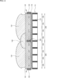
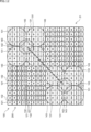
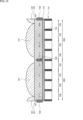
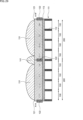
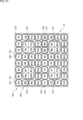
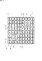
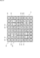
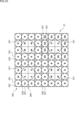
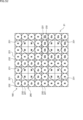
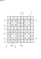
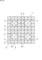
- FIG. 1 is a plan view showing a first example of a structure to which the present disclosure is applied;
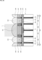
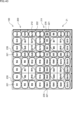
- FIG. 3 is a cross-sectional view corresponding to the planar layout of FIG. 2;
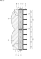
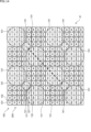
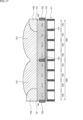
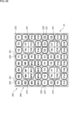
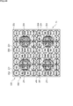
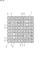
- FIG. 4 is a plan view showing a second example of a structure to which the present disclosure is applied;
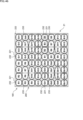
- 5 is a cross-sectional view corresponding to the planar layout of FIG. 4;
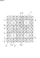
- FIG. 11 is a plan view showing a third example of a structure to which the present disclosure is applied;
- FIG. 7 is a sectional view corresponding to the planar layout of FIG. 6;
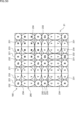
- FIG. 11 is a plan view showing a fourth example of a structure to which the present disclosure is applied;
- FIG. 9 is a sectional view corresponding to the planar layout of FIG. 8;
- FIG. 11 is a plan view showing a fifth example of a structure to which the present disclosure is applied;
- 11 is a cross-sectional view corresponding to the planar layout of FIG. 10;
- FIG. 11 is a plan view showing a sixth example of a structure to which the present disclosure is applied;
- 13 is a cross-sectional view corresponding to the planar layout of FIG. 12;
- FIG. FIG. 21 is a plan view showing a seventh example of a structure to which the present disclosure is applied;
- 15 is a cross-sectional view corresponding to the planar layout of FIG. 14;
- FIG. 20 is a plan view showing an eighth example of a structure to which the present disclosure is applied;
- FIG. 17 is a cross-sectional view corresponding to the planar layout of FIG. 16;
- FIG. 20 is a plan view showing a ninth example of a structure to which the present disclosure is applied;
- 19 is a sectional view corresponding to the planar layout of FIG. 18;
- FIG. 20 is a plan view showing a tenth example of a structure to which the present disclosure is applied;
- 21 is a cross-sectional view corresponding to the planar layout of FIG. 20;
- FIG. FIG. 20 is a plan view showing an eleventh example of a structure to which the present disclosure is applied;
- 23 is a cross-sectional view corresponding to the planar layout of FIG. 22;
- FIG. 21 is a plan view showing a twelfth example of a structure to which the present disclosure is applied;
- FIG. 25 is a cross-sectional view corresponding to the planar layout of FIG. 24;
- FIG. 21 is a plan view showing a thirteenth example of a structure to which the present disclosure is applied;
- FIG. 27 is a cross-sectional view corresponding to the planar layout of FIG. 26;
- FIG. 22 is a plan view showing a fourteenth example of a structure to which the present disclosure is applied;
- FIG. 29 is a sectional view corresponding to the planar layout of FIG. 28;
- FIG. 10 is a diagram illustrating an example of a manufacturing method including steps of forming a structure to which the present disclosure is applied;
- FIG. 25 is a cross-sectional view corresponding to the planar layout of FIG. 24;
- FIG. 21 is a plan view showing a thirteenth example of a structure to which the present disclosure is applied;
- FIG. 27 is a cross
- FIG. 31 is a diagram showing a planar layout corresponding to the cross-sectional view of FIG. 30; 1 is a plan view showing a first example of a structure to which the present disclosure is applied; FIG. FIG. 4 is a cross-sectional view for explaining the effects of a structure to which the present disclosure is applied; FIG. 4 is a cross-sectional view for explaining the effects of a structure to which the present disclosure is applied; FIG. 4 is a cross-sectional view showing an example of the structure of an on-chip microlens; FIG. 4 is a cross-sectional view showing an example of the structure of a CF separating portion; FIG. 4 is a plan view showing a second example of a structure to which the present disclosure is applied; FIG.
- FIG. 11 is a plan view showing a third example of a structure to which the present disclosure is applied;
- FIG. 11 is a plan view showing a fourth example of a structure to which the present disclosure is applied;
- FIG. 11 is a plan view showing a fifth example of a structure to which the present disclosure is applied;
- FIG. 11 is a plan view showing a sixth example of a structure to which the present disclosure is applied;
- FIG. 21 is a plan view showing a seventh example of a structure to which the present disclosure is applied;
- FIG. 20 is a plan view showing an eighth example of a structure to which the present disclosure is applied;
- FIG. 20 is a plan view showing a ninth example of a structure to which the present disclosure is applied;
- FIG. 20 is a plan view showing a tenth example of a structure to which the present disclosure is applied;
- FIG. 20 is a plan view showing a tenth example of a structure to which the present disclosure is applied;
- FIG. 20 is a plan view showing a tenth example of a structure to which the present disclosure is applied;
- FIG. 20 is a plan view showing a tenth example of a structure to which the present disclosure is applied;
- FIG. 20 is a plan view showing an eleventh example of a structure to which the present disclosure is applied;
- FIG. 20 is a plan view showing an eleventh example of a structure to which the present disclosure is applied;
- FIG. 20 is a plan view showing an eleventh example of a structure to which the present disclosure is applied;
- FIG. 20 is a plan view showing an eleventh example of a structure to which the present disclosure is applied;
- FIG. 20 is a plan view showing an eleventh example of a structure to which the present disclosure is applied;
- FIG. 20
- FIG. 20 is a plan view showing an eleventh example of a structure to which the present disclosure is applied;
- FIG. 20 is a plan view showing an eleventh example of a structure to which the present disclosure is applied;
- FIG. 20 is a plan view showing an eleventh example of a structure to which the present disclosure is applied;
- FIG. 20 is a plan view showing an eleventh example of a structure to which the present disclosure is applied;
- 1 is a block diagram showing a configuration example of an electronic device equipped with a photodetector to which the present disclosure is applied;
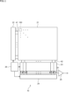
- FIG. 1 is a diagram showing a configuration example of a solid-state imaging device to which the present disclosure is applied.
- the solid-state imaging device 10 is a CMOS (Complementary Metal Oxide Semiconductor) type image sensor.
- the solid-state imaging device 10 is an example of a photodetector to which the present disclosure is applied.
- the solid-state imaging device 10 includes a pixel array section 21 , a vertical driving section 22 , a signal processing section 23 , a horizontal driving section 24 , an output section 25 and a control section 26 .
- the pixel array section 21 has a plurality of pixels 100 arranged two-dimensionally on a substrate made of silicon (Si).
- the pixel 100 has a photoelectric conversion region made up of a photodiode (PD).
- PD photodiode
- a pixel drive line 41 is formed for each row and connected to the vertical drive section 22, and a vertical signal line 42 is formed for each column. is connected to the signal processing unit 23 via the
- the vertical driving section 22 is configured by a shift register, an address decoder, etc., and drives each pixel 100 arranged in the pixel array section 21 . Pixel signals output from the pixels 100 selectively scanned by the vertical driving section 22 are supplied to the signal processing section 23 through the vertical signal lines 42 .
- the signal processing unit 23 performs predetermined signal processing on pixel signals output from each pixel 100 in the selected row through the vertical signal line 42 for each pixel column of the pixel array unit 21 .
- the signal processing for example, processing such as readout processing and noise removal processing is performed.
- the horizontal driving section 24 is composed of a shift register, an address decoder, etc., and selects unit circuits corresponding to the pixel columns of the signal processing section 23 in order. By selective scanning by the horizontal drive unit 24 , pixel signals processed by the signal processing unit 23 are output to the output unit 25 through the horizontal signal line 51 .
- the output unit 25 performs predetermined signal processing on the pixel signals sequentially input from each of the signal processing units 23 through the horizontal signal line 51, and outputs the resulting signal.
- the control unit 26 includes a timing generator or the like that generates various timing signals, and drives the vertical driving unit 22, the signal processing unit 23, the horizontal driving unit 24, etc. based on the various timing signals generated by the timing generator. control.
- FIG. 1 An example (first embodiment) of a structure including pixels 100 arranged two-dimensionally in the pixel array section 21 in the solid-state imaging device 10 will be described with reference to FIGS. 2 to 31.
- FIG. 1 An example (first embodiment) of a structure including pixels 100 arranged two-dimensionally in the pixel array section 21 in the solid-state imaging device 10 will be described with reference to FIGS. 2 to 31.
- FIG. 1 An example (first embodiment) of a structure including pixels 100 arranged two-dimensionally in the pixel array section 21 in the solid-state imaging device 10 will be described with reference to FIGS. 2 to 31.
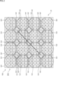
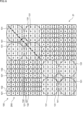
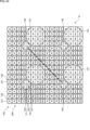
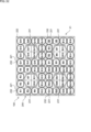
- FIG. 2 is a plan view showing a first example of a structure to which the present disclosure is applied.
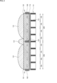
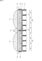
- FIG. 3 is a cross-sectional view showing the A1-A1' cross section in the planar layout of FIG.
- each square arranged in the row direction and the column direction represents a pixel 100.
- colors corresponding to red (R), green (G), and blue (B) are displayed.
- a filter 121 is arranged.
- abbreviations “R”, “Gr”, “Gb”, and “B” representing the colors of the color filters 121 are shown in regions corresponding to the color filters 121 arranged in the pixels 100 . It describes identification information in combination with a number that identifies each area. In FIG. 3 as well, in the area corresponding to the color filter 121, identification information is described in which an abbreviation representing a color and a number are combined.
- R color filters 121-R1 to R16 that transmit a wavelength corresponding to red (R) are arranged are configured as R pixels.
- the R pixel portion is configured by 4 ⁇ 4 R pixels.
- a Gr pixel portion is composed of 4 ⁇ 4 Gr pixels, and a Gb pixel portion is composed of 4 ⁇ 4 Gb pixels.
- a B pixel portion is composed of 4 ⁇ 4 B pixels.
- the R pixel section, the Gr pixel section, the Gb pixel section, and the B pixel section are regularly arranged to form a Bayer array.
- the Bayer array is an array pattern in which G pixels are arranged in a checkered pattern, and R pixels and B pixels are alternately arranged in each row in the remaining portion.
- the arrangement pattern shown in FIG. 2 is repeatedly arranged in the pixel array section 21 .
- One on-chip microlens 131 is arranged for the 4 ⁇ 4 R pixels forming the R pixel portion.
- the structure in which one on-chip microlens 131 is shared by (the color filters 121 of) the 4 ⁇ 4 pixels 100 is also called a 4 ⁇ 4 OCL structure.
- the pixel unit 200 having the 4 ⁇ 4 OCL structure may be configured as a pixel unit (normal pixel unit) that generates a signal for generating a captured image according to subject light, or as a pixel unit for performing phase difference detection. It may be configured as a pixel section (phase difference pixel section) that generates a signal.
- each color there is a gap portion, which is an area where the on-chip microlens 131 arranged in the pixel portion 200 does not exist.
- the gap portion is a region near the on-chip microlens 131 and is a region where the on-chip microlens 131 does not exist. The sensitivity of the pixels 100 in the gap portion is lowered.
- one on-chip microlens 141 is arranged for each gap portion near four on-chip microlenses 131 . As a result, it is possible to suppress a decrease in the sensitivity of the pixels 100 in the gap portion.
- one on-chip microlens 131 is arranged in each of the Gb pixel portion and the Gr pixel portion.
- the Gb pixels in which the G color filters 121-Gb13 are arranged and the Gr pixels in which the G color filters 121-Gr4 are arranged are partially present in the gap portion.
- An on-chip microlens 141 is arranged on the G color filter 121-Gb13 and the G color filter 121-Gr4.
- the Gb pixel portion and the Gr pixel portion have a 4 ⁇ 4 OCL structure, but the Gb pixel in which the G color filter 121-Gb13 is arranged and the Gr pixel in which the G color filter 121-Gr4 is arranged are located in the gap portion. As such, those G pixels are in a 2x2 OCL structure.
- pixel 100 has a photoelectric conversion region formed on silicon substrate 111 .
- a pixel 100 is separated from other adjacent pixels by a pixel separating portion 112 .
- the pixel isolation section 112 is made up of an element isolation structure such as DTI (Deep Trench Isolation).
- An antireflection film 113 is formed on the upper surface of the silicon substrate 111 .
- the gap portion existing in the center of each of the four pixel units 200 By arranging the 2 ⁇ 2 OCL in the gap portion, the decrease in sensitivity of the pixels 100 existing in the gap portion is suppressed.
- the structure in which 2 ⁇ 2 OCLs are arranged in the gap portion is shown, but the structure of the on-chip microlenses arranged in the gap portion is not limited to the 2 ⁇ 2 OCL structure. do not have.
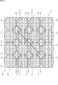
- FIG. 4 is a plan view showing a second example of a structure to which the present disclosure is applied.
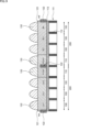
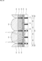
- FIG. 5 is a cross-sectional view showing the A2-A2' cross section in the planar layout of FIG.
- parts corresponding to those in FIGS. 2 and 3 are denoted by the same reference numerals, and description thereof will be omitted as appropriate. Also in the subsequent drawings, the description of the parts with the same reference numerals will be omitted as appropriate.
- one inner lens 142 is arranged in each gap portion near the on-chip microlenses 131 arranged in each of the four adjacent pixel units 200 .
- one on-chip microlens 131 is arranged in each of the Gb pixel portion and the Gr pixel portion.
- the Gb pixels in which the G color filters 121-Gb13 are arranged and the Gr pixels in which the G color filters 121-Gr4 are arranged are partially present in the gap portion.
- An inner lens 142 is arranged on the G color filter 121-Gb13 and the G color filter 121-Gr4.
- the inner lens 142 is an on-chip microlens formed inside the on-chip microlens 131 .
- the gap portion existing in the center of each of the four pixel units 200 is By arranging an OCL (inner lens) in the gap portion, a decrease in sensitivity of the pixel 100 existing in the gap portion is suppressed.
- the on-chip microlenses arranged in the gap portion need not be all inner lenses.
- 2 ⁇ 2 OCL may be placed in a part of . That is, the structure may be a combination of the first example of the structure and the second example of the structure.
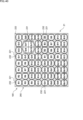
- FIG. 6 is a plan view showing a third example of a structure to which the present disclosure is applied.
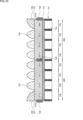
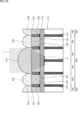
- FIG. 7 is a cross-sectional view showing the A3-A3' cross section in the planar layout of FIG.
- the structure shown in the planar layout of FIG. 6 includes a 1 ⁇ 1 OCL structure in addition to the 4 ⁇ 4 OCL structure compared to the structure shown in the planar layout of FIG. It has a combined structure.
- the pixel portions 200 of each color of red (R), green (G), and blue (B) are arranged in a Bayer array.
- An area in which one on-chip microlens 131 is arranged for the entire area and an area in which one on-chip microlens 132 is arranged for each pixel constituting the pixel section 200 of each color are included.
- the structure in which one on-chip microlens 132 is arranged in (the color filter 121 of) one pixel 100 is also called 1 ⁇ 1 OCL.
- the four pixel units 200 in the upper right and lower left areas have a 4 ⁇ 4 OCL structure
- the four pixel units in the upper left and lower right areas have a 4 ⁇ 4 OCL structure
- 200 becomes a 1 ⁇ 1 OCL structure.
- one on-chip microlens 141 is arranged in a gap portion, which is a region where the on-chip microlenses 131 arranged in the pixel units 200 of each color do not exist, to form a 2 ⁇ 2 OCL structure.
- one on-chip microlens 131 is arranged in each of the Gr pixel portion and the Gb pixel portion.
- the Gr pixels in which the G color filters 121-Gr13 are arranged and the Gb pixels in which the G color filters 121-Gb4 are arranged are partially present in the gap portion.
- An on-chip microlens 141 is arranged on the G color filter 121-Gr13 and the G color filter 121-Gb4.
- the 4 ⁇ 4 OCL structure and the 1 ⁇ 1 OCL structure for the pixel portions 200 of each color arranged in the Bayer arrangement when combining the 4 ⁇ 4 OCL structure and the 1 ⁇ 1 OCL structure for the pixel portions 200 of each color arranged in the Bayer arrangement, the 4 ⁇ 4 OCL structure and the 1 ⁇ 1 OCL structure are combined.
- the 2 ⁇ 2 OCL in the gap portion present in the central portion of each of the four pixel portions 200 By arranging the 2 ⁇ 2 OCL in the gap portion present in the central portion of each of the four pixel portions 200, the decrease in sensitivity of the pixels 100 present in the gap portion is suppressed.
- misalignment may occur where the on-chip microlenses are shifted from their intended positions, but the 4x4 OCL structure is combined with the 1x1 OCL structure Thus, even if misalignment occurs, the influence of the same-color sensitivity difference can be reduced.
- FIG. 8 is a plan view showing a fourth example of the structure to which the present disclosure is applied.
- FIG. 9 is a cross-sectional view showing the A4-A4' cross section in the planar layout of FIG.
- the structure shown in the planar layout of FIG. It has a structure that further combines the structure of (PDAF pixel).
- phase detection pixel 110 used for phase detection auto focus (PDAF) is provided in an area where one on-chip microlens 132 is arranged for each pixel that constitutes the pixel unit 200. .
- one on-chip microlens 133 is arranged for every two phase difference pixels 110 .
- the four pixel units 200 in the upper right and lower left areas have a 4 ⁇ 4 OCL structure
- the four pixel units in the upper left and lower right areas have a 4 ⁇ 4 OCL structure
- 200 is a 1 ⁇ 1 OCL structure including phase difference pixels 110 .
- one on-chip microlens 141 is arranged in a gap portion, which is a region where the on-chip microlenses 131 arranged in the pixel units 200 of each color do not exist, to form a 2 ⁇ 2 OCL structure.
- the central four pixels have the structure of the phase difference pixels 110, and the surrounding regions excluding the central four pixels have the 1 ⁇ 1 OCL structure.
- one on-chip microlens 132 is arranged for each Gb pixel in which the G color filters 121-Gb1 to Gb3 are arranged.
- one on-chip microlens 133 is arranged for the phase difference pixel 110 to be shared with the paired phase difference pixel.
- one on-chip microlens 132 is arranged for each B pixel in which the B color filters 121-B2 to 121-B4 are arranged.
- one on-chip microlens 133 shared with a pair of phase difference pixels is arranged for the phase difference pixel 110 .
- the 4 ⁇ 4 OCL structure, the 1 ⁇ 1 OCL structure, and the PDAF structure are combined for the pixel units 200 of each color arranged in the Bayer array
- the 4 ⁇ 4 By arranging 2 ⁇ 2 OCLs in the gap portion present in the center of each of the four pixel portions 200 having the 4OCL structure, a decrease in sensitivity of the pixels 100 present in the gap portion is suppressed.
- phase difference information acquired by the phase difference pixels 110 can be used.
- the phase difference information acquired by the phase difference pixels 110 can be used.
- the phase difference information acquired by the phase difference pixels 110 can be used.
- the phase difference information acquired by the phase difference pixels 110 can be used.
- the effect of the same color sensitivity difference can be reduced.
- FIG. 10 is a plan view showing a fifth example of a structure to which the present disclosure is applied.
- FIG. 11 is a cross-sectional view showing the A5-A5' cross section in the planar layout of FIG.
- one on-chip microlens 131 is arranged in each of the Gr pixel portion and the Gb pixel portion.
- the Gr pixels in which the G color filters 121-Gr13 are arranged and the Gb pixels in which the G color filters 121-Gb4 are arranged are partially present in the gap portion.
- An inner lens 142 is arranged on the G color filter 121-Gr13 and the G color filter 121-Gb4.
- the 4 ⁇ 4 OCL structure and the 1 ⁇ 1 OCL structure are combined.
- the OCL inner lens
- the decrease in sensitivity of the pixels 100 present in the gap portion is suppressed.
- the effect of the same color sensitivity difference can be reduced.
- FIG. 12 is a plan view showing a sixth example of the structure to which the present disclosure is applied.
- FIG. 13 is a cross-sectional view showing the A6-A6' cross section in the planar layout of FIG.
- the structure shown in the planar layout of FIG. A chip microlens 143 is further arranged.
- one Two inner lenses 142 are arranged in the 4 ⁇ 4 OCL structure.
- one on-chip microlens 143 is arranged in a different-color gap portion, which is a gap portion between (the pixels 100 of) different-color pixel portions 200 in the pixel portion 200 having the 4 ⁇ 4 OCL structure. .
- one on-chip microlens 131 is arranged in each of the Gb pixel portion and the Gr pixel portion.
- the Gb pixel portion a portion of the Gb pixel where the G color filter 121-Gb4 is arranged exists in the gap portion, so the inner lens 142 is arranged above the G color filter 121-Gb4.
- the inner lens 142 is arranged on the G color filters 121-Gr13 because a part of the Gr pixels where the G color filters 121-Gr13 are arranged exists in the gap portion.
- the 4 ⁇ 4 OCL structure and the 1 ⁇ 1 OCL structure are combined.
- an OCL inner lens
- an OCL on-chip microlens 143
- the effect of the same color sensitivity difference can be reduced.
- the gap portion may have a 2 ⁇ 2 OCL structure.
- FIG. 14 is a plan view showing a seventh example of the structure to which the present disclosure is applied.
- 15 is a sectional view showing the A7-A7' section in the planar layout of FIG. 14.
- the structure shown in the planar layout of FIG. 14 is a structure in which the 4 ⁇ 4 OCL structure and the 1 ⁇ 1 OCL structure are combined, similar to the structure shown in the planar layout of FIG. Although it has a 2 OCL structure, it differs in that the Gr pixel portion and Gb pixel portion have a 4 ⁇ 4 OCL structure, while the R pixel portion and B pixel portion have a 1 ⁇ 1 OCL structure.
- the pixel portions 200 of each color of red (R), green (G), and blue (B) are arranged in a Bayer array.
- One on-chip microlens 131 is arranged for the entire pixel, and one on-chip microlens 132 is arranged for each pixel constituting the R pixel portion and the B pixel portion.
- the area shown in the plan view of FIG. 14 is divided into four, in each area, one on-chip microlens 131 is placed in the gap between the two on-chip microlenses 131 arranged in the Gr pixel portion and the Gb pixel portion.
- a lens 141 is arranged to form a 2 ⁇ 2 OCL structure.
- some pixels in the R pixel portion and the B pixel portion have a 2 ⁇ 2 OCL structure instead of a 1 ⁇ 1 OCL structure.
- the R pixel in which the R color filter 121-R16 is arranged and the B pixel in which the B color filter 121-B1 is arranged have a 2 ⁇ 2 OCL structure.
- one on-chip microlens 131 is arranged in each of the Gb pixel portion and the Gr pixel portion.
- the Gb pixels in which the G color filters 121-Gb4 are arranged and the Gr pixels in which the G color filters 121-Gr13 are arranged are partially present in the gap portion.
- An on-chip microlens 141 is arranged on the G color filter 121-Gb4 and the G color filter 121-Gr13.
- the Gr pixel portion and the Gb pixel portion arranged in the Bayer arrangement have a 4 ⁇ 4 OCL structure and the R pixel portion and the B pixel portion have a 1 ⁇ 1 OCL structure
- 4 By arranging the 2 ⁇ 2 OCL in the gap portion of the ⁇ 4 OCL, the decrease in sensitivity of the pixels 100 existing in the gap portion is suppressed. Further, by making the Gr pixel portion and the Gb pixel portion into the 4 ⁇ 4 OCL structure, the sensitivity of the Gr pixel and the Gb pixel can be improved.
- the phase difference information can be obtained from the phase difference pixel portion.
- all of the Gr pixel portion and the Gb pixel portion have a 4 ⁇ 4 OCL structure.
- the remaining Gr pixel portion and Gb pixel portion may have a 1 ⁇ 1 OCL structure.
- FIG. 16 is a plan view showing an eighth example of a structure to which the present disclosure is applied.
- 17 is a sectional view showing the A8-A8' section in the planar layout of FIG. 16.
- the structure shown in the planar layout of FIG. 16 has an inner lens 142 instead of the on-chip microlens 141, compared to the structure shown in the planar layout of FIG.
- one inner lens 142 is arranged for each gap near the on-chip microlens 131 arranged in each of the Gr pixel section and the Gb pixel section.
- one on-chip microlens 131 is arranged in each of the Gb pixel portion and the Gr pixel portion.
- the Gb pixels in which the G color filters 121-Gb4 are arranged and the Gr pixels in which the G color filters 121-Gr13 are arranged are partially present in the gap portion.
- An inner lens 142 is arranged on the filter 121-Gb4 and the G color filter 121-Gr13.
- the Gr pixel portion and the Gb pixel portion arranged in the Bayer arrangement have a 4 ⁇ 4 OCL structure and the R pixel portion and the B pixel portion have a 1 ⁇ 1 OCL structure
- 4 By arranging the OCL (inner lens) in the gap portion of the ⁇ 4 OCL, the decrease in sensitivity of the pixels 100 existing in the gap portion is suppressed. Further, by making the Gr pixel portion and the Gb pixel portion into the 4 ⁇ 4 OCL structure, the sensitivity of the Gr pixel and the Gb pixel can be improved.
- the phase difference information can be obtained from the phase difference pixel portion.
- all of the Gr pixel portion and the Gb pixel portion have a 4 ⁇ 4 OCL structure.
- the remaining Gr pixel portion and Gb pixel portion may have a 1 ⁇ 1 OCL structure.
- FIG. 18 is a plan view showing a ninth example of a structure to which the present disclosure is applied.
- 19 is a sectional view showing the A9-A9' section in the planar layout of FIG. 18.
- the structure shown in the planar layout of FIG. 18 is, like the structure shown in the planar layout of FIG. although it has a 2 OCL structure, it differs in that the R pixel portion has a 4 ⁇ 4 OCL structure, while the G pixel portion and B pixel portion have a 1 ⁇ 1 OCL structure.
- the pixel portions 200 of each color of red (R), green (G), and blue (B) are arranged in a Bayer array.
- One on-chip microlens 131 is arranged, and one on-chip microlens 132 is arranged for each pixel constituting the Gr pixel portion, the Gb pixel portion, and the B pixel portion.
- the Gr pixel and the Gb pixel in which the G color filters 121-Gr13 and Gb4 are arranged and the B pixel in which the B color filter 121-B1 is arranged are two pixels. It becomes a ⁇ 2 OCL structure.
- one on-chip microlens 132 is arranged for each Gb pixel in which the G color filters 121-Gb7, Gb10, and Gb13 are arranged. Since the Gb pixel in which the G color filter 121-Gb4 is arranged has a 2 ⁇ 2 OCL structure, the on-chip microlens 141 is arranged. In the Gr pixel portion, one on-chip microlens 132 is arranged for each Gr pixel in which the G color filters 121-Gr4, Gr7, and Gr10 are arranged. Since the Gr pixel in which the G color filters 121-Gr13 are arranged has a 2 ⁇ 2 OCL structure, an on-chip microlens 141 is arranged.
- the ninth example of the structure when the R pixel portion arranged in the Bayer array has a 4 ⁇ 4 OCL structure and the G pixel portion and the B pixel portion have a 1 ⁇ 1 OCL structure, a gap of 4 ⁇ 4 OCL is obtained.
- a decrease in sensitivity of the pixels 100 existing in the gap portion is suppressed.
- the R pixel portion have a 4 ⁇ 4 OCL structure, it is possible to improve the sensitivity of the R pixel.
- Phase difference information can be acquired by using the R pixel portion of the 4 ⁇ 4 OCL structure as the phase difference pixel portion.
- a structure in which the entire R pixel portion has a 4 ⁇ 4 OCL structure is shown. It may be a 1OCL structure.
- FIG. 20 is a plan view showing a tenth example of a structure to which the present disclosure is applied.
- FIG. 21 is a cross-sectional view showing the A10-A10' cross section in the planar layout of FIG.
- the structure shown in the planar layout of FIG. 20 has an inner lens 142 instead of the on-chip microlens 141 compared to the structure shown in the planar layout of FIG.
- one inner lens 142 is arranged for each gap portion near one on-chip microlens 131 arranged in the R pixel portion.
- one on-chip microlens 132 is arranged for each Gb pixel and Gr pixel in which the G color filter 121 is arranged.
- the inner lens 142 is arranged in the Gb pixel where the G color filter 121-Gb4 is arranged and the Gr pixel where the G color filter 121-Gr13 is arranged.
- a structure in which all of the R pixel portions have a 4 ⁇ 4 OCL structure is shown. It may be a 1OCL structure.
- FIG. 22 is a plan view showing an eleventh example of a structure to which the present disclosure is applied.
- FIG. 23 is a cross-sectional view showing the A11-A11' cross section in the planar layout of FIG.
- the structure shown in the planar layout of FIG. 22 is a structure in which the 4 ⁇ 4 OCL structure and the 1 ⁇ 1 OCL structure are combined, similar to the structure shown in the planar layout of FIG. It has a 2 OCL structure, but differs in that the B pixel portion has a 4 ⁇ 4 OCL structure, while the R pixel portion and the G pixel portion have a 1 ⁇ 1 OCL structure.
- pixel portions 200 of each color of red (R), green (G), and blue (B) are arranged in a Bayer array.
- One on-chip microlens 131 is arranged, and one on-chip microlens 132 is arranged for each pixel constituting the R pixel portion, the Gr pixel portion, and the Gb pixel portion.
- the R pixel in which the R color filters 121-R16 are arranged and the Gr pixel and Gb pixel in which the G color filters 121-Gr13 and Gb4 are arranged are two pixels. It becomes a ⁇ 2 OCL structure.
- one on-chip microlens 132 is arranged for each Gb pixel and Gr pixel in which the G color filter 121 is arranged.
- the on-chip microlens 141 is arranged.
- the B pixel portion arranged in the Bayer array has a 4 ⁇ 4 OCL structure and the R pixel portion and the G pixel portion have a 1 ⁇ 1 OCL structure
- a gap of 4 ⁇ 4 OCL is obtained.
- the 2 ⁇ 2 OCL in the portion a decrease in sensitivity of the pixels 100 existing in the gap portion is suppressed.
- the B pixel portion have a 4 ⁇ 4 OCL structure, the sensitivity of the B pixel can be improved.
- Phase difference information can be acquired by using the B pixel portion of the 4 ⁇ 4 OCL structure as the phase difference pixel portion.
- all of the B pixel portions have a 4 ⁇ 4 OCL structure. It may be a 1OCL structure.
- FIG. 24 is a plan view showing a twelfth example of a structure to which the present disclosure is applied.
- FIG. 25 is a cross-sectional view showing the A12-A12' cross section in the planar layout of FIG.
- the structure shown in the planar layout of FIG. 24 has an inner lens 142 instead of the on-chip microlens 141 compared to the structure shown in the planar layout of FIG.
- one inner lens 142 is arranged for each gap portion near one on-chip microlens 131 arranged in the B pixel portion.
- one on-chip microlens 132 is arranged for each Gb pixel and Gr pixel in which the G color filter 121 is arranged.
- the inner lens 142 is arranged in the Gb pixel where the G color filter 121-Gb4 is arranged and the Gr pixel where the G color filter 121-Gr13 is arranged.
- all of the B pixel portions have a 4 ⁇ 4 OCL structure. It may be a 1OCL structure.
- FIG. 26 is a plan view showing a thirteenth example of a structure to which the present disclosure is applied.
- FIG. 27 is a cross-sectional view showing the A13-A13' cross section in the planar layout of FIG.
- the structure shown in the planar layout of FIG. 26 has a 3 ⁇ 3 OCL structure instead of a 4 ⁇ 4 OCL structure for the pixel section 200 of each color.
- the pixel portions 200 of each color of red (R), green (G), and blue (B) are arranged in a Bayer array. It has a structure in which one on-chip microlens 134 is arranged for the whole.
- one on-chip microlens 134 is arranged for 3 ⁇ 3 R pixels forming the R pixel portion.
- the structure in which one on-chip microlens 134 is shared by (the color filters 121 of) the 3 ⁇ 3 pixels 100 is also called a 3 ⁇ 3 OCL structure.
- one on-chip microlens 144 is arranged for each gap portion near four on-chip microlenses 134 . As a result, it is possible to suppress a decrease in the sensitivity of the pixels 100 in the gap portion.
- one on-chip microlens 134 is arranged in each of the Gb pixel portion and the Gr pixel portion. Further, in the Gb pixel portion and the Gr pixel portion, the Gb pixels in which the G color filters 121-Gb7 are arranged and the Gr pixels in which the G color filters 121-Gr3 are arranged are partially present in the gap portion. An on-chip microlens 144 is arranged on the G color filter 121-Gb7 and the G color filter 121-Gr3.
- the Gb pixel portion and the Gr pixel portion have a 3 ⁇ 3 OCL structure, but the Gb pixel in which the G color filter 121-Gb7 is arranged and the Gr pixel in which the G color filter 121-Gr3 is arranged are located in the gap portion. As such, those G pixels are in a 2x2 OCL structure.
- the gap portion existing in the center of each of the four pixel units 200 By arranging the 2 ⁇ 2 OCL in the gap portion, the decrease in sensitivity of the pixels 100 existing in the gap portion is suppressed.
- the 3 ⁇ 3 OCL structure and the 4 ⁇ 4 OCL structure were exemplified as the structure of the pixel unit 200 for each color.
- the pixel unit 200 composed of n ⁇ n pixels corresponding to n ⁇ n array color filters of the same color.
- at least a part of the pixel units 200 of each color arranged in a predetermined arrangement pattern has an n ⁇ n OCL structure, which is a structure in which one on-chip microlens is shared by n ⁇ n pixels, and the n ⁇ n OCL structure Another on-chip microlens can be arranged in the gap portion near the on-chip microlens.
- FIG. 28 is a plan view showing a fourteenth example of a structure to which the present disclosure is applied.
- FIG. 29 is a cross-sectional view showing the A14-A14' cross section in the planar layout of FIG.
- the structure shown in the plan view of FIG. 28 uses color filters 121 corresponding to cyan (C), magenta (M), and yellow (Y). It's becoming
- abbreviations “Y”, “C”, “G”, and “M” representing the colors of the color filters 121 are added to the regions corresponding to the color filters 121 arranged in the pixels 100 . It describes identification information in combination with a number that identifies each area. In FIG. 29 as well, in the area corresponding to the color filter 121, identification information is described that is a combination of an abbreviation representing a color and a number.
- 4 ⁇ 4 16 pixels in which Y color filters 121-Y1 to Y16 that transmit a wavelength corresponding to yellow (Y) are arranged are configured as Y pixels.
- a Y pixel portion is composed of 4 ⁇ 4 Y pixels.
- the 4 ⁇ 4 16 pixels in which the C color filters 121-C1 to C16 that transmit the wavelength corresponding to cyan (C) are arranged are configured as C pixels.
- a C pixel portion is composed of 4 ⁇ 4 C pixels.
- a G pixel portion is composed of 4 ⁇ 4 G pixels.
- the 4 ⁇ 4 16 pixels in which the M color filters 121-M1 to M16 that transmit the wavelength corresponding to magenta (M) are arranged are configured as M pixels.
- An M pixel portion is composed of 4 ⁇ 4 M pixels.
- one on-chip microlens 131 is arranged for 16 pixels of 4 ⁇ 4, and a 4 ⁇ 4 OCL structure is formed. It's becoming In FIG. 28 , one on-chip microlens 141 is arranged for each gap portion near four on-chip microlenses 131 . As a result, it is possible to suppress a decrease in the sensitivity of the pixels 100 in the gap portion.
- one on-chip microlens 131 is arranged in each of the G pixel portion and the C pixel portion. Further, in the G pixel portion and the C pixel portion, part of the G pixels in which the G color filters 121-G13 are arranged and the C pixels in which the C color filters 121-C4 are arranged exist in the gap portion.
- An on-chip microlens 141 is arranged on the G color filter 121-G13 and the C color filter 121-C4.
- the color filter 121 is not limited to color filters corresponding to red (R), green (G), and blue (B), but cyan (C), magenta (M), and yellow (Y). Even in a structure using corresponding color filters, by arranging 2 ⁇ 2 OCL in the gap near the on-chip microlens 141 of 4 ⁇ 4 OCL, it is possible to suppress the decrease in sensitivity of the pixels 100 existing in the gap. .
- the C pixel portion, the M pixel portion, and the Y pixel portion are examples of the pixel portion 200 other than the RGB pixels.
- a color pixel unit 200 may be employed.
- FIG. FIGS. 30A to 30C show cross-sectional structures corresponding to dashed lines on the planar layouts of FIGS. 31A to 31C.
- steps after forming a pixel separating portion 112 and an antireflection film 113 on a silicon substrate 111 on which a photoelectric conversion region is formed are shown in order of steps.
- a CF separating portion 122 made of a light shielding material or the like is formed on the antireflection film 113 .
- color filters 121 corresponding to each color are formed.
- an on-chip microlens 131 is formed in the pixel portion 200 having the 4 ⁇ 4 OCL structure, and an on-chip microlens 141 is formed in a gap portion near the on-chip microlens 131 .
- FIG. do Another example (second embodiment) of the structure including the pixels 100 arranged two-dimensionally in the pixel array section 21 in the solid-state imaging device 10 will be described with reference to FIGS. 32 to 55.
- FIG. do Another example (second embodiment) of the structure including the pixels 100 arranged two-dimensionally in the pixel array section 21 in the solid-state imaging device 10 will be described with reference to FIGS. 32 to 55.
- FIG. do Another example (second embodiment) of the structure including the pixels 100 arranged two-dimensionally in the pixel array section 21 in the solid-state imaging device 10
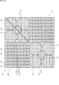
- FIG. 32 is a plan view showing a first example of a structure to which the present disclosure is applied; 33 is a cross-sectional view showing a cross section including the R pixel portion and the Gr pixel portion in the planar layout of FIG. 32.
- FIG. 32 is a plan view showing a first example of a structure to which the present disclosure is applied; 33 is a cross-sectional view showing a cross section including the R pixel portion and the Gr pixel portion in the planar layout of FIG. 32.
- each square arranged in the row direction and the column direction represents a pixel 100.
- colors corresponding to red (R), green (G), and blue (B) are displayed.
- a filter 221 is arranged.
- abbreviations “R”, “Gr”, “Gb”, and “B” representing the colors of the color filters 221 are shown in regions corresponding to the color filters 221 arranged in the pixels 100 . It describes identification information in combination with a number that identifies each area.
- abbreviations representing colors are written in regions corresponding to the color filters 121 .
- the arrangement pattern shown in FIG. 32 is repeatedly arranged in the pixel array section 21, and the R pixel section, the Gr pixel section, the Gb pixel section, and the B pixel section are arranged in a Bayer arrangement.
- one ON signal is applied to R pixels surrounded by pixels of the same color (R pixels), that is, 2 ⁇ 2 R pixels in which R color filters 221-R6, R7, R10, and R11 are arranged.
- a chip microlens 231 is arranged.
- the structure in which one on-chip microlens 231 is shared by (the color filters 221 of) the 2 ⁇ 2 pixels 100 is also called a 2 ⁇ 2 OCL structure.
- the 2 ⁇ 2 pixels 100 (4 pixels) of the 2 ⁇ 2 OCL structure may be configured as pixels (normal pixels) that generate signals for generating a captured image according to subject light, or may be configured as pixels (normal pixels) for generating a captured image according to subject light. It may be configured as a pixel (phase difference pixel) that generates a signal for detection.
- the R pixels adjacent to the different color pixels that is, the 12 R pixels in which the R color filters 221-R1 to R5, R8, R9, and R12 to R16 are arranged are , one on-chip microlens 232 is arranged for each pixel.
- the structure in which one on-chip microlens 232 is arranged in (the color filter 221 of) one pixel 100 is also called a 1 ⁇ 1 OCL structure.
- R pixels surrounded by pixels of the same color have a 2 ⁇ 2 OCL structure
- R pixels adjacent to pixels of a different color have a 1 ⁇ 1 OCL structure
- the 2 ⁇ 2 arranged R color filter 221 corresponding to the 2 ⁇ 2 OCL structure is separated from the surrounding 1 ⁇ 1 arranged R color filter 221 corresponding to the 1 ⁇ 1 OCL structure by the CF separator 222 .
- the 1 ⁇ 1 array R color filter 221 corresponding to the 1 ⁇ 1 OCL structure corresponds to the other 1 ⁇ 1 array color filter 221 corresponding to the 1 ⁇ 1 OCL structure and the 2 ⁇ 2 OCL structure to the CF separator 222. It is separated from the R color filter 221 arranged in a 2 ⁇ 2 array.
- a Gr pixel surrounded by pixels of the same color has a 2 ⁇ 2 OCL structure
- a Gr pixel adjacent to a pixel of a different color has a 1 ⁇ 1 OCL structure
- Gb pixels surrounded by pixels of the same color have a 2 ⁇ 2 OCL structure
- Gb pixels adjacent to pixels of different colors have a 1 ⁇ 1 OCL structure
- B pixels surrounded by pixels of the same color have a 2 ⁇ 2 OCL structure
- B pixels adjacent to pixels of a different color (G pixels) have a 1 ⁇ 1 OCL structure.
- the cross-sectional view of FIG. 34 shows, for comparison, a structure in which all 16 pixels (4 ⁇ 4 pixels) of the same color in the pixel section 200 have a 2 ⁇ 2 OCL structure.
- the 4 ⁇ 4 pixels of the pixel portion 200 for each color are divided into four, and one on-chip microlens 231 is arranged for each 2 ⁇ 2 pixels to form four 2 ⁇ 2 OCL structures.
- the pixels surrounding the Gr pixel in the 2 ⁇ 2 OCL structure are different pixels (for example, R pixels) from the Gr pixel, so that the trench separation scattering causes a large amount of color mixing between different colors.
- the structure shown in the cross-sectional view of FIG. 33 includes a 1 ⁇ 1 OCL structure compared to the structure shown in the cross-sectional view of FIG. can be done.
- the pixel 100 has a photoelectric conversion region formed on the silicon substrate 211.
- a pixel 100 is separated from other adjacent pixels by a pixel separating portion 212 .
- the pixel isolation section 212 is composed of an element isolation structure such as DTI.
- the 2 ⁇ 2 array of G color filters 221 corresponding to the 2 ⁇ 2 OCL structure and the 1 ⁇ 1 array of G color filters 221 corresponding to the 1 ⁇ 1 OCL structure are separated by the CF separator 222 .
- the 1 ⁇ 1 arranged G color filter 221 corresponding to the 1 ⁇ 1 OCL structure and the 1 ⁇ 1 arranged R color filter 221 corresponding to the 1 ⁇ 1 OCL structure are separated by the CF separator 222 .
- An antireflection film 213 is formed on the upper surface of the silicon substrate 211 .
- the Gr pixel portion has been described, but in the R pixel portion, the Gb pixel portion, and the B pixel portion, pixels surrounded by pixels of the same color have a 2 ⁇ 2 OCL structure, and pixels adjacent to pixels of different colors are formed. has a 1 ⁇ 1 OCL structure, it is possible to greatly reduce the difference in sensitivity between the same color due to color mixture and to greatly reduce the color mixture between different colors due to trench separation scattering.
- FIG. 35 is a cross-sectional view showing an example of the structure of the on-chip microlenses 231 and 232 in the first example of the structure.
- Gr pixels central 2 ⁇ 2 pixels surrounded by pixels of the same color (Gr pixels) have a 2 ⁇ 2 OCL structure, and Gr pixels adjacent to different color pixels (R pixels or B pixels) are formed. (the surrounding 12 pixels) has a 1 ⁇ 1 OCL structure.
- the height of the on-chip microlenses 231 arranged in the 2 ⁇ 2 OCL structure is higher than the height of the on-chip microlenses 232 arranged in the 1 ⁇ 1 OCL structure.
- the on-chip microlens 231 By keeping the height of the on-chip microlens 231 high in this way, the spot diameter D of the incident light (L in the figure) on the upper surface of the silicon substrate 211 can be reduced, and the separation ratio can be improved.
- the on-chip microlens 232 can improve the quantum efficiency (QE) by reducing the height. This makes it possible to eliminate the trade-off between the isolation ratio of the 2 ⁇ 2 OCL structure and the quantum efficiency (QE) of the 1 ⁇ 1 OCL structure.
- FIG. 36 is a cross-sectional view showing an example of the structure of the CF isolation portion 222 in the first example of the structure.
- Gr pixels central 2 ⁇ 2 pixels surrounded by pixels of the same color (Gr pixels) have a 2 ⁇ 2 OCL structure, and Gr pixels adjacent to different color pixels (R pixels or B pixels) are formed. (the surrounding 12 pixels) has a 1 ⁇ 1 OCL structure.
- the width of the CF separating portion 222 separating the periphery of the 2 ⁇ 2 arrayed G color filters 221 corresponding to the 2 ⁇ 2 OCL structure is 1 ⁇ 1 array corresponding to the 1 ⁇ 1 OCL structure. is wider than the width of the CF separating portion 222 that separates the periphery of the G color filter 221 from .
- the CF separating portion 222 made of a low refractive index material or the like strengthens light collection and improves the separation ratio.
- the on-chip microlens 232 can improve the quantum efficiency (QE) by reducing the height. This makes it possible to eliminate the trade-off between the isolation ratio of the 2 ⁇ 2 OCL structure and the quantum efficiency (QE) of the 1 ⁇ 1 OCL structure.
- the Gr pixel portion has been described here, the same applies to the R pixel portion, the Gb pixel portion, and the B pixel portion.
- the structure shown in the cross-sectional view of FIG. 35 or the structure shown in the cross-sectional view of FIG. 36 can be adopted.
- FIG. 37 is a plan view showing a second example of a structure to which the present disclosure is applied;
- parts corresponding to those in FIG. 32 are denoted by the same reference numerals, and description thereof will be omitted as appropriate. Also in the subsequent drawings, the description of the parts with the same reference numerals will be omitted as appropriate.
- a Y pixel surrounded by pixels of the same color (Y pixels) has a 2 ⁇ 2 OCL structure
- a Y pixel adjacent to a pixel of a different color (R pixel or B pixel) has a 1 ⁇ 1 OCL structure.
- pixels surrounded by pixels of the same color have a 2 ⁇ 2 OCL structure, and pixels adjacent to pixels of different colors have a 2 ⁇ 2 OCL structure.
- the x1 OCL structure can reduce the difference in sensitivity between the same colors due to color mixture.
- the SNR can be improved by reducing color mixture between different colors due to trench isolation scattering.
- FIG. 38 is a plan view showing a third example of a structure to which the present disclosure is applied.
- an M pixel portion, a Y pixel portion, and a C pixel portion are arranged in a MYYC arrangement.
- M pixels surrounded by pixels of the same color (M pixels) have a 2 ⁇ 2 OCL structure
- M pixels adjacent to pixels of a different color (Y pixels) have a 1 ⁇ 1 OCL structure.
- a Y pixel surrounded by pixels of the same color (Y pixels) has a 2 ⁇ 2 OCL structure
- a Y pixel adjacent to a pixel of a different color (M pixel or C pixel) has a 1 ⁇ 1 OCL structure.
- C pixels in which the C color filters 221-C1 to C16 that transmit the wavelength corresponding to cyan (C) are arranged are configured as C pixels.
- C pixels surrounded by pixels of the same color (C pixels) have a 2 ⁇ 2 OCL structure
- C pixels adjacent to pixels of a different color (Y pixels) have a 1 ⁇ 1 OCL structure.
- pixels surrounded by pixels of the same color have a 2 ⁇ 2 OCL structure, and pixels adjacent to pixels of different colors have a 2 ⁇ 2 OCL structure.
- the x1 OCL structure can reduce the difference in sensitivity between the same colors due to color mixture.
- the SNR can be improved by reducing color mixture between different colors due to trench isolation scattering.
- CMY color filters are exemplified as the color filters 221 other than the RGB color filters, but the present invention is not limited to this, and other color filters may be used.
- the C pixel portion, the M pixel portion, and the Y pixel portion are examples of the pixel portion 200 other than the RGB pixels.
- a color pixel unit 200 may be employed.
- Quantum efficiency (QE) can be improved by using not only RGB color filters but also CMY color filters.
- FIG. 39 is a plan view showing a fourth example of a structure to which the present disclosure is applied.
- the structure shown in the planar layout of FIG. 32 Compared with the structure shown in the planar layout of FIG. 32, the structure shown in the planar layout of FIG. The ratio of the ⁇ 1 OCL structure is increased.
- pixels surrounded by pixels of the same color have a 2 ⁇ 2 OCL structure, and pixels adjacent to pixels of different colors have a 1 ⁇ 1 OCL structure.
- R pixels surrounded by pixels of the same color (R pixels) and R pixels adjacent to pixels of a different color (Gr pixels or Gb pixels), that is, all R pixels are set to 1 ⁇ . It has a 1OCL structure.
- B pixels surrounded by pixels of the same color (B pixels) and B pixels adjacent to pixels of different colors (Gr pixels or Gb pixels), that is, all B pixels are formed into a 1 ⁇ 1 OCL structure.
- the Gr pixel portion and the Gb pixel portion include a 2 ⁇ 2 OCL structure, whereas the R pixel portion and the B pixel portion have a 2 ⁇ 2 OCL structure.
- the ratio of the 1 ⁇ 1 OCL structure to the whole can be increased.
- the MTF can be improved and the resolution can be increased. Therefore, when the resolution is emphasized, the fourth example of the structure is adopted, and at least one of the pixel units 200 is used instead of using all the pixel units 200 as phase difference pixel units that acquire phase difference information.
- the part may be the phase difference pixel part.
- FIG. 40 is a plan view showing a fifth example of a structure to which the present disclosure is applied.
- the structure shown in the planar layout of FIG. 39 Compared with the structure shown in the planar layout of FIG. 39, the structure shown in the planar layout of FIG. structure to further increase the proportion of 1 ⁇ 1 OCL structure.
- pixels surrounded by pixels of the same color have a 2 ⁇ 2 OCL structure, and pixels adjacent to pixels of different colors have a 1 ⁇ 1 OCL structure.
- pixels adjacent to pixels of different colors have a 1 ⁇ 1 OCL structure.
- pixels surrounded by pixels of the same color and pixels adjacent to pixels of a different color, that is, all pixels have a 1 ⁇ 1 OCL structure.
- the Gr pixel unit includes a 2 ⁇ 2 OCL structure, but the R pixel unit, the B pixel unit, and the Gb pixel unit have 2 ⁇ 2 OCL structures.
- the ratio of the 1 ⁇ 1 OCL structure to the whole can be increased. Resolution can be increased by increasing the proportion of 1 ⁇ 1 OCL structures.
- the R pixel portion and the B pixel portion have a 1 ⁇ 1 OCL structure. It is not necessary to have a 1 OCL structure, and a part of the R pixel portion and B pixel portion has only a 1 ⁇ 1 OCL structure, and the remaining R pixel portion and B pixel portion have a 2 ⁇ 2 OCL structure and a 1 ⁇ 1 OCL structure. You may do so.
- the 2 ⁇ 2 OCL structure may be arranged in places, and the ratio of the 2 ⁇ 2 OCL structure and the 1 ⁇ 1 OCL structure to the whole is arbitrary.
- FIG. 41 is a plan view showing a sixth example of a structure to which the present disclosure is applied.
- the structure shown in the planar layout of FIG. 32 Compared with the structure shown in the planar layout of FIG. 32, the structure shown in the planar layout of FIG. Only four pixels in the central portion of the pixel portion and the B pixel portion have a 2 ⁇ 2 OCL structure.
- pixels surrounded by pixels of the same color have a 2 ⁇ 2 OCL structure, and pixels adjacent to pixels of different colors have a 1 ⁇ 1 OCL structure.
- pixels surrounded by pixels of the same color and pixels adjacent to pixels of a different color that is, all pixels, have a 1 ⁇ 1 OCL structure.
- the R pixel portion and the B pixel portion include a 2 ⁇ 2 OCL structure, whereas the Gr pixel portion and the Gb pixel portion have a 2 ⁇ 2 OCL structure.
- the sensitivity of the R pixel portion and the B pixel portion can be increased. That is, since the sensitivity of the R pixel portion and the B pixel portion is relatively low compared to that of the Gr pixel portion and the Gb pixel portion, the four pixels in the central portion have a 2 ⁇ 2 OCL structure to increase the sensitivity.
- FIG. 42 is a plan view showing a seventh example of a structure to which the present disclosure is applied.
- phase difference information can be obtained from pixels adjacent to pixels of different colors.
- an R pixel surrounded by pixels of the same color has a 2 ⁇ 2 OCL structure
- an R pixel adjacent to a pixel of a different color has a 1 ⁇ 1 OCL structure and a 1 ⁇ 1 OCL structure. It has either a 2 OCL structure or a 2 ⁇ 1 OCL structure.
- one on-chip microlens 231 is arranged on the whole, and 2 ⁇ 2OCL structure.
- One on-chip microlens 232 is arranged for each R pixel (one pixel) in which the R color filters 221-R1, R4, R13, and R16 are arranged, forming a 1 ⁇ 1 OCL structure.
- One on-chip microlens 233 is arranged for each 1 ⁇ 2 R pixel (2 pixels) in which the R color filters 221-R2 and R3 are arranged, forming a 1 ⁇ 2 OCL structure.
- 1 ⁇ 2 R pixels (two pixels) in which the R color filters 221-R14 and R15 are arranged have a 1 ⁇ 2 OCL structure.
- the structure in which one on-chip microlens 233 is shared by (the color filters 221 of) the 1 ⁇ 2 pixels 100 is also called a 1 ⁇ 2 OCL structure.
- One on-chip microlens 234 is arranged for each 2 ⁇ 1 R pixel (2 pixels) in which the R color filters 221-R5 and R9 are arranged, forming a 2 ⁇ 1 OCL structure.
- the 2 ⁇ 1 R pixel (2 pixels) in which the R color filters 221-R8 and R12 are arranged has a 2 ⁇ 1 OCL structure.
- the structure in which one on-chip microlens 234 is shared by (the color filters 221 of) the 2 ⁇ 1 pixels 100 is also called a 2 ⁇ 1 OCL structure.
- phase difference information can be obtained by using R pixels with a 2 ⁇ 2 OCL structure as phase difference pixels.
- the R pixel of the 1 ⁇ 2 OCL structure or the 2 ⁇ 1 OCL structure can be used as the phase difference pixel.
- pixels surrounded by pixels of the same color have a 2 ⁇ 2 OCL structure
- pixels adjacent to pixels of different colors have a 1 ⁇ 1 OCL structure and a 1 ⁇ 2 OCL structure. structure, and 2 ⁇ 1 OCL structure.
- pixels surrounded by pixels of the same color have a 2 ⁇ 2 OCL structure
- pixels adjacent to pixels of a different color have a structure of:
- the phase difference pixels can be increased by including a 1 ⁇ 2 OCL structure or a 2 ⁇ 1 OCL structure. Even if the structure shown in the planar layout of FIG. 42 is employed, color mixing between different colors due to trench isolation scattering does not increase significantly.
- FIG. 43 is a plan view showing an eighth example of a structure to which the present disclosure is applied.
- the R color filter 221 and the on-chip microlens 235 arranged in each R pixel have different positions and sizes for each R pixel.
- the color filter 221 and the on-chip microlens 235 arranged in each pixel are different in position and size for each pixel.
- the CF separating portion 222 formed between the color filters 221 differs in position and size for each pixel.
- the R pixel By changing the positions and sizes of the color filter 221, the CF separation unit 222, and the on-chip microlens 235 for each pixel 100 that is an R pixel, a Gr pixel, a Gb pixel, or a B pixel, the R pixel
- the positions and sizes of the color filter 221, the CF separation section 222, and the on-chip microlens 235 are changed for each pixel section 200, which is a section, a Gr pixel section, a Gb pixel section, or a B pixel section.
- the eighth example of the structure by changing the positions and sizes of the color filter 221, the CF separation unit 222, and the on-chip microlens 235 for each pixel 100 or pixel unit 200, It is also possible to reduce the difference in sensitivity between the same colors due to mixed color components other than trench separation scattering.
- the color filter 221, the CF separator 222, and the on-chip microlens 235 may be changed for each pixel 100 or pixel unit 200, but at least one structure may also be changed. Also, when changing the structure, at least one of the position and the size may be changed. In other words, when viewed as the pixel units 200 of each color, the position or size may be different as a whole.
- FIG. 44 is a plan view showing a ninth example of a structure to which the present disclosure is applied.
- the structure shown in the plan layout of FIG. 32 has a different refractive index from the on-chip microlens 232 .
- the effective refractive index of one on-chip microlens 231 arranged in the 2 ⁇ 2 R pixels in which the R color filters 221-R6, R7, R10, and R11 are arranged is the R color filter 221- It is higher than the effective refractive index of the 12 on-chip microlenses 232 arranged in each of the 12 R pixels in which R1 to R5, R8, R9 and R12 to R16 are arranged.
- the effective refractive index of the on-chip microlenses 231 arranged in a 2 ⁇ 2 OCL structure composed of pixels surrounded by pixels of the same color is set to 1. It is made higher than the effective refractive index of the on-chip microlenses 232 arranged in the ⁇ 1 OCL structure.
- the effective refractive index of the on-chip microlenses 231 with the 2 ⁇ 2 OCL structure is the same as the effective refractive index of the on-chip microlenses 232 with the 1 ⁇ 1 OCL structure.
- (Tenth example of structure) 45 to 48 are plan views showing a tenth example of the structure to which the present disclosure is applied.
- the structure shown in the planar layout of FIG. 45 is different from the structure shown in the planar layout of FIG. Phase difference information is obtained from pixels surrounded by pixels.
- R pixels surrounded by pixels of the same color have a 2 ⁇ 1 OCL structure
- R pixels adjacent to pixels of different colors have a 1 ⁇ 1 OCL structure.
- the on-chip microlens 234 is arranged for the 2 ⁇ 1 R pixels (2 pixels) in which the R color filters 221-R6 and R10 are arranged, forming a 2 ⁇ 1 OCL structure.
- an on-chip microlens 234 is arranged for the 2 ⁇ 1 R pixel (2 pixels) where the R color filters 221-7 and R11 are arranged, forming a 2 ⁇ 1 OCL structure.
- An on-chip microlens 232 is arranged for each of the R pixels (12 pixels) in which the R color filters 221-R1 to R5, R8, R9, R12 to R16 are arranged, forming a 1 ⁇ 1 OCL structure.
- pixels surrounded by pixels of the same color have a 2 ⁇ 1 OCL structure, and pixels adjacent to pixels of different colors have a 1 ⁇ 1 OCL structure.
- pixels surrounded by pixels of the same color have a 2 ⁇ 1 OCL structure, and two 2 pixels arranged side by side in the row direction.
- a pixel with a ⁇ 1 OCL structure is made available as a phase difference pixel.
- pixels surrounded by pixels of the same color have a 2 ⁇ 1 OCL structure, but as shown in the planar layout of FIG. A ⁇ 2 OCL structure may be used.
- FIG. 46 two 1 ⁇ 2 OCL structure pixels arranged side by side in the column direction can be used as phase difference pixels.
- either a 2.times.1 OCL structure or a 1.times.2 OCL structure is adopted for each pixel portion 200 of each color, and the 2.times.1 OCL structure and the 1.times.2 OCL structure are adopted.
- a combined structure is also possible.
- the central four pixels of the R pixel portion and the B pixel portion have a 1 ⁇ 2 OCL structure, while the central four pixels of the Gr pixel portion and the Gb pixel portion have a 2 ⁇ 1 OCL structure.
- the central four pixels of the R pixel portion and the B pixel portion have a 2 ⁇ 1 OCL structure
- the central four pixels of the Gr pixel portion and the Gb pixel portion have a 1 ⁇ 2 OCL structure.
- the color of the color filter 221 can be changed between the phase difference pixels for acquiring the phase difference information and the other pixels. At that time, by combining the color filters 221 corresponding to red (R), green (G), and blue (B) with the color filters 221 corresponding to other colors, color reproducibility can be ensured. .
- color filters 221 corresponding to red (R), green (G), and blue (B) with the color filters 221 corresponding to other colors, color reproducibility can be ensured.
- other colors for example, cyan (C), magenta (M), yellow (Y), white (W), emerald (E), wide green, and other green colors can be used to increase the sensitivity. can be improved.
- Example 1 As shown in the planar layout of FIG. 49, in the pixel section 200, when four pixels in the central portion having a 2 ⁇ 2 OCL structure are used as phase difference pixels, four pixels with a 2 ⁇ 2 OCL structure and a 1 ⁇ 1 OCL structure around them are used. 12 pixels, the color of the color filter 221 can be changed.
- the Y color filter 221 is arranged in the four pixels of the 2 ⁇ 2 OCL structure, and the 12 pixels of the 1 ⁇ 1 OCL structure are arranged around them.
- a G color filter 221 is arranged in the pixel.
- M color filters 221 are arranged in 4 pixels of the 2 ⁇ 2 OCL structure, and R color filters 221 are arranged in the surrounding 12 pixels of the 1 ⁇ 1 OCL structure.
- C color filters 221 are arranged in 4 pixels of 2 ⁇ 2 OCL structure, and B color filters 221 are arranged in the surrounding 12 pixels of 1 ⁇ 1 OCL structure.
- Example 2 As shown in the planar layout of FIG. 50, in the pixel section 200, four pixels in the central portion having a 2 ⁇ 2 OCL structure, two pixels in the upper and lower portions of the 1 ⁇ 2 OCL structure, and two pixels in the left and right portions thereof.
- the color filter 221 is composed of 12 pixels of the 2 ⁇ 2 OCL structure, the 1 ⁇ 2 OCL structure, and the 2 ⁇ 1 OCL structure, and the other 4 pixels of the 1 ⁇ 1 OCL structure. can change the color of
- the Y color filters 221 are arranged in 12 pixels of the 2 ⁇ 2 OCL structure, the 1 ⁇ 2 OCL structure, and the 2 ⁇ 1 OCL structure.
- a G color filter 221 is arranged for four pixels of the 1 ⁇ 1 OCL structure.
- M color filters 221 are arranged in 12 pixels of 2 ⁇ 2 OCL structure, 1 ⁇ 2 OCL structure, and 2 ⁇ 1 OCL structure, and R color filters are arranged in 4 pixels of 1 ⁇ 1 OCL structure.
- a filter 221 is arranged.
- C color filters 221 are arranged in 12 pixels of 2 ⁇ 2 OCL structure, 1 ⁇ 2 OCL structure, and 2 ⁇ 1 OCL structure, and B color filters 221 are arranged in 4 pixels of 1 ⁇ 1 OCL structure. are placed.
- Example 3 As shown in the planar layout of FIG. 51, in the pixel section 200, when four pixels in the central portion having a 2 ⁇ 2 OCL structure are used as phase difference pixels, four pixels with a 2 ⁇ 2 OCL structure and a 1 ⁇ 1 OCL structure around them are used. 12 pixels, the color of the color filter 221 can be changed.
- the G color filters 221 of green color are arranged in the four pixels of the 2 ⁇ 2 OCL structure, and the surrounding 1 A G color filter 221 is arranged for 12 pixels of the ⁇ 1 OCL structure.
- the upper right pixel portion 200 four pixels of the 2 ⁇ 2 OCL structure are W pixels without color filters, and the surrounding 12 pixels of the 1 ⁇ 1 OCL structure are provided with R color filters 221.
- the lower left pixel section 200 4 pixels of the 2 ⁇ 2 OCL structure are W pixels without color filters, and B color filters 221 are arranged on the surrounding 12 pixels of the 1 ⁇ 1 OCL structure.
- Example 4 As shown in the planar layout of FIG. 52, in the pixel section 200, when four pixels in the central portion having a 2 ⁇ 2 OCL structure are used as phase difference pixels, four pixels with a 2 ⁇ 2 OCL structure and a 1 ⁇ 1 OCL structure around them are used. 12 pixels, the color of the color filter 221 can be changed.
- four pixels of the 2 ⁇ 2 OCL structure are W pixels without color filters.
- G color filters 221 are arranged in 12 pixels of the 1 ⁇ 1 OCL structure.
- R color filter 221 is arranged for 12 pixels of the 1 ⁇ 1 OCL structure.
- B color filters 221 are arranged in 12 pixels of the 1 ⁇ 1 OCL structure.
- Example 5 As shown in the planar layout of FIG. 53, in the pixel section 200, four pixels in the central portion having a 2 ⁇ 2 OCL structure, or two pixels in the upper and lower portions of the 1 ⁇ 2 OCL structure, and two pixels in the left and right portions thereof.
- 12 pixels of the 2 ⁇ 2 OCL structure, the 1 ⁇ 2 OCL structure, and the 2 ⁇ 1 OCL structure, and the other 4 pixels of the 1 ⁇ 1 OCL structure are used for color filters. 221 color can be changed.
- four pixels of the 2 ⁇ 2 OCL structure are W pixels without color filters, and E color filters 221 are arranged for eight pixels of the 1 ⁇ 2 OCL structure and the 2 ⁇ 1 OCL structure. be.
- G color filters 221 are arranged in four pixels of the 1 ⁇ 1 OCL structure.
- an R color filter 221 is arranged for four pixels of the 1 ⁇ 1 OCL structure.
- B color filters 221 are arranged in four pixels of the 1 ⁇ 1 OCL structure.
- Example 6 As shown in the planar layout of FIG. 54, in the pixel section 200, when four pixels in the central portion having a 2 ⁇ 2 OCL structure are used as phase difference pixels, four pixels with a 2 ⁇ 2 OCL structure and a 1 ⁇ 1 OCL structure around them are used. 12 pixels, the color of the color filter 221 can be changed.
- the G color filter 221 is arranged in the four pixels of the 2 ⁇ 2 OCL structure, and the surrounding 12 pixels of the 1 ⁇ 1 OCL structure are arranged. , a C color filter 221 is arranged.
- B color filters 221 are arranged in 4 pixels of the 2 ⁇ 2 OCL structure, and M color filters 221 are arranged in the surrounding 12 pixels of the 1 ⁇ 1 OCL structure.
- R color filters 221 are arranged in 4 pixels of 2 ⁇ 2 OCL structure, and Y color filters 221 are arranged in the surrounding 12 pixels of 1 ⁇ 1 OCL structure.
- the G color filter 221 is arranged in the four pixels of the 2 ⁇ 2 OCL structure, and the surrounding 12 pixels of the 1 ⁇ 1 OCL structure are arranged. , a C color filter 221 is arranged.
- B color filters 221 are arranged in 4 pixels of the 2 ⁇ 2 OCL structure, and G color filters 221 are arranged in the surrounding 12 pixels of the 1 ⁇ 1 OCL structure.
- R color filters 221 are arranged in 4 pixels of 2 ⁇ 2 OCL structure, and Y color filters 221 are arranged in the surrounding 12 pixels of 1 ⁇ 1 OCL structure.
- the eleventh example of the structure by changing the color of the color filter 221 between the phase difference pixels for acquiring the phase difference information and the other pixels, for example, color reproducibility is ensured. or to improve sensitivity.
- the pixel unit 200 of each color has a structure composed of 4 ⁇ 4 pixels corresponding to a 4 ⁇ 4 array of color filters of the same color. It can be applied to the pixel unit 200 composed of n ⁇ n pixels corresponding to color filters in an n ⁇ n arrangement (n is an integer of 2 or more). That is, in the present disclosure, the pixel unit 200 of each color is made up of n ⁇ n pixels corresponding to the same-color n ⁇ n array of color filters, and the pixel unit 200 of each color is surrounded by pixels of the same color.
- the structure for arranging the on-chip microlenses is made different between the pixels with different colors and the pixels adjacent to the pixels with different colors.
- any one of the first to fourteenth examples of the structure in the first embodiment may be combined with any other structure. do not have. Also, any one of the first to eleventh examples of the structure in the second embodiment may be combined with any other structure.
- the solid-state imaging device 10 is a CMOS-type solid-state imaging device, and has an upper layer (back side) on the side opposite to a wiring layer side (front side) formed in a lower layer when viewed from a silicon substrate on which a photoelectric conversion region is formed. It can be a back-illuminated structure in which light is incident from the substrate. Note that the solid-state imaging device 10 may have a surface irradiation type structure in which the light incident side is the wiring layer side (surface side).
- CMOS complementary metal-oxide-semiconductor
- CCD Charge Coupled Device
- FIG. 56 is a block diagram showing a configuration example of an electronic device equipped with a photodetector to which the present disclosure is applied.
- an electronic device 1000 includes an optical system 1011 including a lens group, a photodetector 1012 having a function and structure corresponding to the solid-state imaging device 10 of FIG. ) 1013.
- a CPU Central Processing Unit
- a frame memory 1014 In the electronic device 1000, in addition to the imaging system, a CPU (Central Processing Unit) 1010, a frame memory 1014, a display 1015, an operation system 1016, an auxiliary memory 1017, a communication I/F 1018, and a power supply system 1019 are connected via a bus 1020. It becomes the composition connected mutually.
- a CPU Central Processing Unit
- a CPU 1010 controls the operation of each part of the electronic device 1000 .
- the optical system 1011 takes in incident light (image light) from a subject and forms an image on the photodetection surface of the photodetection element 1012 .
- the photodetector 1012 converts the amount of incident light imaged on the photodetection surface by the optical system 1011 into an electric signal for each pixel and outputs the electric signal as a pixel signal.
- the DSP 1013 performs predetermined signal processing on the signal output from the photodetector 1012 .
- the frame memory 1014 temporarily records image data of still images or moving images captured by the imaging system.
- a display 1015 is a liquid crystal display or an organic EL display, and displays still images or moving images captured by the imaging system.
- the operation system 1016 issues operation commands for various functions of the electronic device 1000 according to user's operations.
- the auxiliary memory 1017 is a storage medium including semiconductor memory such as flash memory, and records image data of still images or moving images captured by the imaging system.
- the communication I/F 1018 has a communication module compatible with a predetermined communication method, and transmits image data of still images or moving images captured by the imaging system to other devices via a network.
- the power supply system 1019 appropriately supplies various types of power as operating power to the CPU 1010, DSP 1013, frame memory 1014, display 1015, operation system 1016, auxiliary memory 1017, and communication I/F 1018.
- on-chip microlenses may be read as on-chip lenses (OCL).
- the present disclosure can be configured as follows.
- a photodetector in which a first on-chip microlens and a second on-chip microlens different from the first on-chip microlens are arranged in at least a part of a pixel portion composed of n ⁇ n pixels.
- the pixel unit is composed of n ⁇ n pixels corresponding to color filters of the same color in an n ⁇ n array, At least part of the pixel portion has an n ⁇ n OCL structure, which is a structure in which one on-chip microlens is shared by n ⁇ n pixels, The light according to (1) above, wherein another on-chip microlens is arranged in a gap portion which is an area near the on-chip microlens of the n ⁇ n OCL structure and is an area where the on-chip microlens does not exist. detection device.
- the pixel unit is composed of 4 ⁇ 4 pixels corresponding to a 4 ⁇ 4 array of color filters of the same color, All or part of the pixel portion has a 4 ⁇ 4 OCL structure, which is a structure in which one on-chip microlens is shared by 4 ⁇ 4 pixels,
- a part of the pixel portion has a 1 ⁇ 1 OCL structure, which is a structure in which one on-chip microlens is arranged in one pixel,
- the gap portion is a different color gap portion existing between different color pixel portions among the pixel portions having the 4 ⁇ 4 OCL structure and the 1 ⁇ 1 OCL structure when the 4 ⁇ 4 OCL structure and the 1 ⁇ 1 OCL structure are combined.
- the photodetector according to (5) wherein another on-chip microlens is arranged in the inter-color gap portion.
- the photodetector according to (5) wherein all or part of the pixel portions corresponding to a specific color among the pixel portions have the 4 ⁇ 4 OCL structure.
- All or part of the pixel portion in which the color filter that transmits the wavelength corresponding to blue (B) is arranged has the 4 ⁇ 4 OCL structure.
- the pixel unit is composed of n ⁇ n pixels corresponding to color filters of the same color in an n ⁇ n array, The photodetector according to (1), wherein in the pixel portion, a pixel surrounded by pixels of the same color and a pixel adjacent to a pixel of a different color have different on-chip microlens structures.
- the pixel unit is composed of 4 ⁇ 4 pixels corresponding to a 4 ⁇ 4 array of color filters of the same color, In the pixel portion, pixels surrounded by pixels of the same color have a 2 ⁇ 2 OCL structure, which is a structure in which 2 ⁇ 2 pixels share one on-chip microlens, and pixels adjacent to pixels of different colors are formed into one on-chip micro lens.
- the photodetector according to (16) above which has a 1 ⁇ 1 OCL structure in which a chip microlens is arranged in one pixel.
- the width of the separating portion separating the periphery of the 2 ⁇ 2 array color filters corresponding to the 2 ⁇ 2 OCL structure is the width of the separating portion separating the periphery of the 1 ⁇ 1 array color filters corresponding to the 1 ⁇ 1 OCL structure.
- the color filter is at least one of a color filter transmitting a wavelength corresponding to red (R), a color filter transmitting a wavelength corresponding to green (G), and a color filter transmitting a wavelength corresponding to blue (B).
- the color filter is at least one of a color filter transmitting a wavelength corresponding to cyan (C), a color filter transmitting a wavelength corresponding to magenta (M), and a color filter transmitting a wavelength corresponding to yellow (Y).
- the photodetector according to any one of (17) to (20) above.
- the photodetector according to any one of (17) to (21), wherein at least part of the pixel section is a phase difference pixel section that acquires phase difference information.
- the pixel unit is composed of 4 ⁇ 4 pixels corresponding to a 4 ⁇ 4 array of color filters of the same color, In the pixel portion, pixels surrounded by pixels of the same color have a 2 ⁇ 2 OCL structure, which is a structure in which 2 ⁇ 2 pixels share one on-chip microlens, and pixels adjacent to pixels of different colors are formed into one on-chip micro lens.
- 1 ⁇ 1 OCL structure which is a structure in which a chip microlens is arranged in one pixel
- 1 ⁇ 2 OCL structure which is a structure in which one on-chip microlens is shared by 1 ⁇ 2 pixels, or one on-chip microlens is 2 ⁇ 1
- the photodetector according to (16) above which has a 2 ⁇ 1 OCL structure, which is a structure shared by pixels.
- the pixel unit is composed of 4 ⁇ 4 pixels corresponding to a 4 ⁇ 4 array of color filters of the same color, In the pixel portion, a 1 ⁇ 2 OCL structure in which pixels surrounded by pixels of the same color share one on-chip microlens with 1 ⁇ 2 pixels, or one on-chip microlens with 2 ⁇ 1 pixels.
- the photodetector according to (16) above has a 2 ⁇ 1 OCL structure, which is a shared structure, and a 1 ⁇ 1 OCL structure, which is a structure in which one on-chip microlens is arranged in one pixel for a pixel adjacent to a pixel of a different color.
- Device. (25) The structure of at least one of the on-chip microlenses, the color filters, and the separation section separating the color filters is different for each of the pixel sections in at least one of position and size.
- (26) a plurality of pixels each having a photoelectric conversion region; and an on-chip microlens arranged with respect to the pixel,
- a photodetector in which a first on-chip microlens and a second on-chip microlens different from the first on-chip microlens are arranged in at least a part of a pixel portion composed of n ⁇ n pixels.
- 10 solid-state imaging device 100 pixels, 110 phase difference pixels, 111 silicon substrate, 112 pixel separation section, 121 color filter, 122 CF separation section, 131, 132, 133, 134 on-chip microlens, 141, 143, 144 on-chip Micro lens, 142 Inner lens, 200 Pixel part, 211 Silicon substrate, 212 Pixel separation part, 221 Color filter, 222 CF separation part, 231, 232, 233, 234, 235 On-chip micro lens, 1000 Electronic device, 1012 Photodetector element
Landscapes
- Solid State Image Pick-Up Elements (AREA)
- Transforming Light Signals Into Electric Signals (AREA)
Abstract
Description
図1は、本開示を適用した固体撮像装置の構成例を示す図である。
図2は、本開示を適用した構造の第1の例を示す平面図である。図3は、図2の平面レイアウトにおけるA1-A1'断面を示す断面図である。
図4は、本開示を適用した構造の第2の例を示す平面図である。図5は、図4の平面レイアウトにおけるA2-A2'断面を示す断面図である。図4,図5において、図2,図3と対応する部分には同一の符号を付しており、その説明は適宜省略する。以降の図面においても、同一の符号の部分の説明は適宜省略する。
図6は、本開示を適用した構造の第3の例を示す平面図である。図7は、図6の平面レイアウトにおけるA3-A3'断面を示す断面図である。
図8は、本開示を適用した構造の第4の例を示す平面図である。図9は、図8の平面レイアウトにおけるA4-A4'断面を示す断面図である。
図10は、本開示を適用した構造の第5の例を示す平面図である。図11は、図10の平面レイアウトにおけるA5-A5'断面を示す断面図である。
図12は、本開示を適用した構造の第6の例を示す平面図である。図13は、図12の平面レイアウトにおけるA6-A6'断面を示す断面図である。
図14は、本開示を適用した構造の第7の例を示す平面図である。図15は、図14の平面レイアウトにおけるA7-A7'断面を示す断面図である。
図16は、本開示を適用した構造の第8の例を示す平面図である。図17は、図16の平面レイアウトにおけるA8-A8'断面を示す断面図である。
図18は、本開示を適用した構造の第9の例を示す平面図である。図19は、図18の平面レイアウトにおけるA9-A9'断面を示す断面図である。
図20は、本開示を適用した構造の第10の例を示す平面図である。図21は、図20の平面レイアウトにおけるA10-A10'断面を示す断面図である。
図22は、本開示を適用した構造の第11の例を示す平面図である。図23は、図22の平面レイアウトにおけるA11-A11'断面を示す断面図である。
図24は、本開示を適用した構造の第12の例を示す平面図である。図25は、図24の平面レイアウトにおけるA12-A12'断面を示す断面図である。
図26は、本開示を適用した構造の第13の例を示す平面図である。図27は、図26の平面レイアウトにおけるA13-A13'断面を示す断面図である。
図28は、本開示を適用した構造の第14の例を示す平面図である。図29は、図28の平面レイアウトにおけるA14-A14'断面を示す断面図である。
次に、図30,図31を参照しながら、本開示を適用した構造を形成する工程を含む製造方法の例を説明する。図30のA乃至Cは、図31のA乃至Cの平面レイアウト上の破線に対応した断面構造を示している。この製造方法の例では、光電変換領域を形成したシリコン基板111に、画素分離部112と反射防止膜113を形成した後の工程を工程順に示している。
図32は、本開示を適用した構造の第1の例を示す平面図である。図33は、図32の平面レイアウトにおけるR画素部とGr画素部を含む断面を示す断面図である。
図37は、本開示を適用した構造の第2の例を示す平面図である。図37において、図32と対応する部分には同一の符号を付してあり、その説明は適宜省略する。以降の図面においても、同一の符号の部分の説明は適宜省略する。
図38は、本開示を適用した構造の第3の例を示す平面図である。
図39は、本開示を適用した構造の第4の例を示す平面図である。
図40は、本開示を適用した構造の第5の例を示す平面図である。
図41は、本開示を適用した構造の第6の例を示す平面図である。
図42は、本開示を適用した構造の第7の例を示す平面図である。
図43は、本開示を適用した構造の第8の例を示す平面図である。
図44は、本開示を適用した構造の第9の例を示す平面図である。
図45乃至図48は、本開示を適用した構造の第10の例を示す平面図である。
図49乃至図55は、本開示を適用した構造の第11の例を示す平面図である。
図49の平面レイアウトに示すように、画素部200において、2×2OCL構造となる中央部の4画素を位相差画素として用いる場合、2×2OCL構造の4画素と、その周囲の1×1OCL構造の12画素とで、カラーフィルタ221の色を変えることができる。
図50の平面レイアウトに示すように、画素部200において、2×2OCL構造となる中央部の4画素、並びにその上部と下部の1×2OCL構造の2画素、及びその左部と右部の2×1OCL構造の2画素を位相差画素として用いる場合、2×2OCL構造、1×2OCL構造、及び2×1OCL構造の12画素と、それ以外の1×1OCL構造の4画素とで、カラーフィルタ221の色を変えることができる。
図51の平面レイアウトに示すように、画素部200において、2×2OCL構造となる中央部の4画素を位相差画素として用いる場合、2×2OCL構造の4画素と、その周囲の1×1OCL構造の12画素とで、カラーフィルタ221の色を変えることができる。
図52の平面レイアウトに示すように、画素部200において、2×2OCL構造となる中央部の4画素を位相差画素として用いる場合、2×2OCL構造の4画素と、その周囲の1×1OCL構造の12画素とで、カラーフィルタ221の色を変えることができる。
図53の平面レイアウトに示すように、画素部200において、2×2OCL構造となる中央部の4画素、又はその上部と下部の1×2OCL構造の2画素、及びその左部と右部の2×1OCL構造の2画素を位相差画素として用いる場合、2×2OCL構造と、1×2OCL構造、及び2×1OCL構造の12画素と、それ以外の1×1OCL構造の4画素とで、カラーフィルタ221の色を変えることができる。
図54の平面レイアウトに示すように、画素部200において、2×2OCL構造となる中央部の4画素を位相差画素として用いる場合、2×2OCL構造の4画素と、その周囲の1×1OCL構造の12画素とで、カラーフィルタ221の色を変えることができる。
図55の平面レイアウトに示すように、画素部200において、2×2OCL構造となる中央部の4画素を位相差画素として用いる場合、2×2OCL構造の4画素と、その周囲の1×1OCL構造の12画素とで、カラーフィルタ221の色を変えることができる。
本開示を適用した光検出装置は、スマートフォン、タブレット型端末、携帯電話機、デジタルスチルカメラ、デジタルビデオカメラなどの電子機器に搭載することができる。図56は、本開示を適用した光検出装置を搭載した電子機器の構成例を示すブロック図である。
それぞれが光電変換領域を有する複数の画素と、
画素に対して配置したオンチップマイクロレンズと
を備え、
n×n画素から構成される画素部の少なくとも一部において、第1のオンチップマイクロレンズと、前記第1のオンチップマイクロレンズと異なる第2のオンチップマイクロレンズとが配置される
光検出装置。
(2)
前記画素部は、同色のn×n配列のカラーフィルタに対応したn×n画素から構成され、
前記画素部の少なくとも一部を、1つのオンチップマイクロレンズをn×n画素で共有した構造であるn×nOCL構造とし、
前記n×nOCL構造のオンチップマイクロレンズの近傍の領域であって、当該オンチップマイクロレンズが存在しない領域であるギャップ部に、別のオンチップマイクロレンズを配置する
前記(1)に記載の光検出装置。
(3)
前記画素部は、同色の4×4配列のカラーフィルタに対応した4×4画素から構成され、
前記画素部の全て又は一部を、1つのオンチップマイクロレンズを4×4画素で共有した構造である4×4OCL構造とし、
前記ギャップ部を埋めるように、前記別のオンチップマイクロレンズを配置する
前記(2)に記載の光検出装置。
(4)
前記別のオンチップマイクロレンズの全て又は一部は、インナーレンズである
前記(3)に記載の光検出装置。
(5)
前記画素部の一部を、1つのオンチップマイクロレンズを1画素に配置した構造である1×1OCL構造とし、
前記4×4OCL構造と前記1×1OCL構造とを組み合わせる
前記(3)に記載の光検出装置。
(6)
前記画素部は、位相差情報を取得するための位相差画素を含む
前記(5)に記載の光検出装置。
(7)
前記別のオンチップマイクロレンズの全て又は一部は、インナーレンズである
前記(5)又は(6)に記載の光検出装置。
(8)
前記ギャップ部は、前記4×4OCL構造と前記1×1OCL構造とを組み合わせたときに、前記4×4OCL構造となる前記画素部のうち、異色の画素部の間に存在する異色間ギャップ部を含み、
前記異色間ギャップ部に、さらに別のオンチップマイクロレンズを配置する
前記(5)に記載の光検出装置。
(9)
前記画素部のうち、特定の色に対応した画素部の全て又は一部を、前記4×4OCL構造とする
前記(5)に記載の光検出装置。
(10)
緑(G)に対応する波長を透過するカラーフィルタを配置した画素部の全て又は一部を、前記4×4OCL構造とし、
前記4×4OCL構造の近傍に存在する前記ギャップ部に、前記別のオンチップマイクロレンズを配置する
前記(9)に記載の光検出装置。
(11)
前記別のオンチップマイクロレンズの全て又は一部は、インナーレンズである
前記(10)に記載の光検出装置。
(12)
赤(R)に対応する波長を透過するカラーフィルタを配置した画素部の全て又は一部を、前記4×4OCL構造とし、
前記4×4OCL構造の近傍に存在する前記ギャップ部に、前記別のオンチップマイクロレンズを配置する
前記(9)に記載の光検出装置。
(13)
前記別のオンチップマイクロレンズの全て又は一部は、インナーレンズである
前記(12)に記載の光検出装置。
(14)
青(B)に対応する波長を透過するカラーフィルタを配置した画素部の全て又は一部を、前記4×4OCL構造とし、
前記4×4OCL構造の近傍に存在する前記ギャップ部に、前記別のオンチップマイクロレンズを配置する
前記(9)に記載の光検出装置。
(15)
前記別のオンチップマイクロレンズの全て又は一部は、インナーレンズである
前記(14)に記載の光検出装置。
(16)
前記画素部は、同色のn×n配列のカラーフィルタに対応したn×n画素から構成され、
前記画素部において、同色の画素に囲まれた画素と、異色の画素と隣接する画素とは、オンチップマイクロレンズを配置する構造が異なる
前記(1)に記載の光検出装置。
(17)
前記画素部は、同色の4×4配列のカラーフィルタに対応した4×4画素から構成され、
前記画素部において、同色の画素に囲まれた画素を、1つのオンチップマイクロレンズを2×2画素で共有した構造である2×2OCL構造とし、異色の画素と隣接する画素を、1つのオンチップマイクロレンズを1画素に配置した構造である1×1OCL構造とする
前記(16)に記載の光検出装置。
(18)
前記2×2OCL構造のオンチップマイクロレンズの高さは、前記1×1OCL構造のオンチップマイクロレンズの高さよりも高くなる
前記(17)に記載の光検出装置。
(19)
前記2×2OCL構造に対応した2×2配列のカラーフィルタの周辺を分離する分離部の幅は、前記1×1OCL構造に対応した1×1配列のカラーフィルタの周辺を分離する分離部の幅よりも広くなる
前記(17)に記載の光検出装置。
(20)
前記カラーフィルタは、赤(R)に対応する波長を透過するカラーフィルタ、緑(G)に対応する波長を透過するカラーフィルタ、及び青(B)に対応する波長を透過するカラーフィルタの少なくともいずれかを含む
前記(17)乃至(19)のいずれかに記載の光検出装置。
(21)
前記カラーフィルタは、シアン(C)に対応する波長を透過するカラーフィルタ、マゼンタ(M)に対応する波長を透過するカラーフィルタ、及び黄(Y)に対応する波長を透過するカラーフィルタの少なくともいずれかを含む
前記(17)乃至(20)のいずれかに記載の光検出装置。
(22)
前記画素部の少なくとも一部は、位相差情報を取得する位相差画素部である
前記(17)乃至(21)のいずれかに記載の光検出装置。
(23)
前記画素部は、同色の4×4配列のカラーフィルタに対応した4×4画素から構成され、
前記画素部において、同色の画素に囲まれた画素を、1つのオンチップマイクロレンズを2×2画素で共有した構造である2×2OCL構造とし、異色の画素と隣接する画素を、1つのオンチップマイクロレンズを1画素に配置した構造である1×1OCL構造、1つのオンチップマイクロレンズを1×2画素で共有した構造である1×2OCL構造、又は1つのオンチップマイクロレンズを2×1画素で共有した構造である2×1OCL構造とする
前記(16)に記載の光検出装置。
(24)
前記画素部は、同色の4×4配列のカラーフィルタに対応した4×4画素から構成され、
前記画素部において、同色の画素に囲まれた画素を、1つのオンチップマイクロレンズを1×2画素で共有した構造である1×2OCL構造、又は1つのオンチップマイクロレンズを2×1画素で共有した構造である2×1OCL構造とし、異色の画素と隣接する画素を、1つのオンチップマイクロレンズを1画素に配置した構造である1×1OCL構造とする
前記(16)に記載の光検出装置。
(25)
前記画素部ごとに、前記オンチップマイクロレンズ、前記カラーフィルタ、及び前記カラーフィルタを分離する分離部の少なくとも1つの構造が、位置及び大きさの少なくとも一方で異なる
前記(17)乃至(24)のいずれかに記載の光検出装置。
(26)
それぞれが光電変換領域を有する複数の画素と、
画素に対して配置したオンチップマイクロレンズと
を備え、
n×n画素から構成される画素部の少なくとも一部において、第1のオンチップマイクロレンズと、前記第1のオンチップマイクロレンズと異なる第2のオンチップマイクロレンズとが配置される
光検出装置を搭載した電子機器。
Claims (26)
- それぞれが光電変換領域を有する複数の画素と、
画素に対して配置したオンチップマイクロレンズと
を備え、
n×n画素から構成される画素部の少なくとも一部において、第1のオンチップマイクロレンズと、前記第1のオンチップマイクロレンズと異なる第2のオンチップマイクロレンズとが配置される
光検出装置。 - 前記画素部は、同色のn×n配列のカラーフィルタに対応したn×n画素から構成され、
前記画素部の少なくとも一部を、1つのオンチップマイクロレンズをn×n画素で共有した構造であるn×nOCL構造とし、
前記n×nOCL構造のオンチップマイクロレンズの近傍の領域であって、当該オンチップマイクロレンズが存在しない領域であるギャップ部に、別のオンチップマイクロレンズを配置する
請求項1に記載の光検出装置。 - 前記画素部は、同色の4×4配列のカラーフィルタに対応した4×4画素から構成され、
前記画素部の全て又は一部を、1つのオンチップマイクロレンズを4×4画素で共有した構造である4×4OCL構造とし、
前記ギャップ部を埋めるように、前記別のオンチップマイクロレンズを配置する
請求項2に記載の光検出装置。 - 前記別のオンチップマイクロレンズの全て又は一部は、インナーレンズである
請求項3に記載の光検出装置。 - 前記画素部の一部を、1つのオンチップマイクロレンズを1画素に配置した構造である1×1OCL構造とし、
前記4×4OCL構造と前記1×1OCL構造とを組み合わせる
請求項3に記載の光検出装置。 - 前記画素部は、位相差情報を取得するための位相差画素を含む
請求項5に記載の光検出装置。 - 前記別のオンチップマイクロレンズの全て又は一部は、インナーレンズである
請求項5に記載の光検出装置。 - 前記ギャップ部は、前記4×4OCL構造と前記1×1OCL構造とを組み合わせたときに、前記4×4OCL構造となる前記画素部のうち、異色の画素部の間に存在する異色間ギャップ部を含み、
前記異色間ギャップ部に、さらに別のオンチップマイクロレンズを配置する
請求項5に記載の光検出装置。 - 前記画素部のうち、特定の色に対応した画素部の全て又は一部を、前記4×4OCL構造とする
請求項5に記載の光検出装置。 - 緑(G)に対応する波長を透過するカラーフィルタを配置した画素部の全て又は一部を、前記4×4OCL構造とし、
前記4×4OCL構造の近傍に存在する前記ギャップ部に、前記別のオンチップマイクロレンズを配置する
請求項9に記載の光検出装置。 - 前記別のオンチップマイクロレンズの全て又は一部は、インナーレンズである
請求項10に記載の光検出装置。 - 赤(R)に対応する波長を透過するカラーフィルタを配置した画素部の全て又は一部を、前記4×4OCL構造とし、
前記4×4OCL構造の近傍に存在する前記ギャップ部に、前記別のオンチップマイクロレンズを配置する
請求項9に記載の光検出装置。 - 前記別のオンチップマイクロレンズの全て又は一部は、インナーレンズである
請求項12に記載の光検出装置。 - 青(B)に対応する波長を透過するカラーフィルタを配置した画素部の全て又は一部を、前記4×4OCL構造とし、
前記4×4OCL構造の近傍に存在する前記ギャップ部に、前記別のオンチップマイクロレンズを配置する
請求項9に記載の光検出装置。 - 前記別のオンチップマイクロレンズの全て又は一部は、インナーレンズである
請求項14に記載の光検出装置。 - 前記画素部は、同色のn×n配列のカラーフィルタに対応したn×n画素から構成され、
前記画素部において、同色の画素に囲まれた画素と、異色の画素と隣接する画素とは、オンチップマイクロレンズを配置する構造が異なる
請求項1に記載の光検出装置。 - 前記画素部は、同色の4×4配列のカラーフィルタに対応した4×4画素から構成され、
前記画素部において、同色の画素に囲まれた画素を、1つのオンチップマイクロレンズを2×2画素で共有した構造である2×2OCL構造とし、異色の画素と隣接する画素を、1つのオンチップマイクロレンズを1画素に配置した構造である1×1OCL構造とする
請求項16に記載の光検出装置。 - 前記2×2OCL構造のオンチップマイクロレンズの高さは、前記1×1OCL構造のオンチップマイクロレンズの高さよりも高くなる
請求項17に記載の光検出装置。 - 前記2×2OCL構造に対応した2×2配列のカラーフィルタの周辺を分離する分離部の幅は、前記1×1OCL構造に対応した1×1配列のカラーフィルタの周辺を分離する分離部の幅よりも広くなる
請求項17に記載の光検出装置。 - 前記カラーフィルタは、赤(R)に対応する波長を透過するカラーフィルタ、緑(G)に対応する波長を透過するカラーフィルタ、及び青(B)に対応する波長を透過するカラーフィルタの少なくともいずれかを含む
請求項17に記載の光検出装置。 - 前記カラーフィルタは、シアン(C)に対応する波長を透過するカラーフィルタ、マゼンタ(M)に対応する波長を透過するカラーフィルタ、及び黄(Y)に対応する波長を透過するカラーフィルタの少なくともいずれかを含む
請求項17に記載の光検出装置。 - 前記画素部の少なくとも一部は、位相差情報を取得する位相差画素部である
請求項17に記載の光検出装置。 - 前記画素部は、同色の4×4配列のカラーフィルタに対応した4×4画素から構成され、
前記画素部において、同色の画素に囲まれた画素を、1つのオンチップマイクロレンズを2×2画素で共有した構造である2×2OCL構造とし、異色の画素と隣接する画素を、1つのオンチップマイクロレンズを1画素に配置した構造である1×1OCL構造、1つのオンチップマイクロレンズを1×2画素で共有した構造である1×2OCL構造、又は1つのオンチップマイクロレンズを2×1画素で共有した構造である2×1OCL構造とする
請求項16に記載の光検出装置。 - 前記画素部は、同色の4×4配列のカラーフィルタに対応した4×4画素から構成され、
前記画素部において、同色の画素に囲まれた画素を、1つのオンチップマイクロレンズを1×2画素で共有した構造である1×2OCL構造、又は1つのオンチップマイクロレンズを2×1画素で共有した構造である2×1OCL構造とし、異色の画素と隣接する画素を、1つのオンチップマイクロレンズを1画素に配置した構造である1×1OCL構造とする
請求項16に記載の光検出装置。 - 前記画素部ごとに、前記オンチップマイクロレンズ、前記カラーフィルタ、及び前記カラーフィルタを分離する分離部の少なくとも1つの構造が、位置及び大きさの少なくとも一方で異なる
請求項17に記載の光検出装置。 - それぞれが光電変換領域を有する複数の画素と、
画素に対して配置したオンチップマイクロレンズと
を備え、
n×n画素から構成される画素部の少なくとも一部において、第1のオンチップマイクロレンズと、前記第1のオンチップマイクロレンズと異なる第2のオンチップマイクロレンズとが配置される
光検出装置を搭載した電子機器。
Priority Applications (4)
| Application Number | Priority Date | Filing Date | Title |
|---|---|---|---|
| JP2023551047A JPWO2023053530A1 (ja) | 2021-09-30 | 2022-03-24 | |
| DE112022004674.0T DE112022004674T5 (de) | 2021-09-30 | 2022-03-24 | Photodetektionsvorrichtung und elektronische einrichtung |
| CN202280055093.0A CN117813689A (zh) | 2021-09-30 | 2022-03-24 | 光电检测装置和电子设备 |
| US18/692,499 US20240387583A1 (en) | 2021-09-30 | 2022-03-24 | Photodetector and electronic apparatus |
Applications Claiming Priority (2)
| Application Number | Priority Date | Filing Date | Title |
|---|---|---|---|
| JP2021160953 | 2021-09-30 | ||
| JP2021-160953 | 2021-09-30 |
Publications (1)
| Publication Number | Publication Date |
|---|---|
| WO2023053530A1 true WO2023053530A1 (ja) | 2023-04-06 |
Family
ID=85782187
Family Applications (1)
| Application Number | Title | Priority Date | Filing Date |
|---|---|---|---|
| PCT/JP2022/013973 Ceased WO2023053530A1 (ja) | 2021-09-30 | 2022-03-24 | 光検出装置及び電子機器 |
Country Status (5)
| Country | Link |
|---|---|
| US (1) | US20240387583A1 (ja) |
| JP (1) | JPWO2023053530A1 (ja) |
| CN (1) | CN117813689A (ja) |
| DE (1) | DE112022004674T5 (ja) |
| WO (1) | WO2023053530A1 (ja) |
Citations (4)
| Publication number | Priority date | Publication date | Assignee | Title |
|---|---|---|---|---|
| JP2003523646A (ja) * | 1999-02-25 | 2003-08-05 | ヴィジョンセンス リミテッド | 光学装置 |
| JP2015162493A (ja) * | 2014-02-26 | 2015-09-07 | 株式会社ニコン | 撮像素子および撮像装置 |
| JP2016015430A (ja) * | 2014-07-03 | 2016-01-28 | ソニー株式会社 | 固体撮像素子および電子機器 |
| JP2021015984A (ja) * | 2014-12-18 | 2021-02-12 | ソニー株式会社 | 固体撮像素子、および電子機器 |
Family Cites Families (1)
| Publication number | Priority date | Publication date | Assignee | Title |
|---|---|---|---|---|
| KR102721299B1 (ko) | 2019-11-12 | 2024-10-25 | 삼성전자주식회사 | 이미지 센서, 그것을 포함하는 이미지 장치 및 그것의 동작 방법 |
-
2022
- 2022-03-24 CN CN202280055093.0A patent/CN117813689A/zh not_active Withdrawn
- 2022-03-24 JP JP2023551047A patent/JPWO2023053530A1/ja not_active Abandoned
- 2022-03-24 DE DE112022004674.0T patent/DE112022004674T5/de active Pending
- 2022-03-24 WO PCT/JP2022/013973 patent/WO2023053530A1/ja not_active Ceased
- 2022-03-24 US US18/692,499 patent/US20240387583A1/en active Pending
Patent Citations (4)
| Publication number | Priority date | Publication date | Assignee | Title |
|---|---|---|---|---|
| JP2003523646A (ja) * | 1999-02-25 | 2003-08-05 | ヴィジョンセンス リミテッド | 光学装置 |
| JP2015162493A (ja) * | 2014-02-26 | 2015-09-07 | 株式会社ニコン | 撮像素子および撮像装置 |
| JP2016015430A (ja) * | 2014-07-03 | 2016-01-28 | ソニー株式会社 | 固体撮像素子および電子機器 |
| JP2021015984A (ja) * | 2014-12-18 | 2021-02-12 | ソニー株式会社 | 固体撮像素子、および電子機器 |
Also Published As
| Publication number | Publication date |
|---|---|
| US20240387583A1 (en) | 2024-11-21 |
| JPWO2023053530A1 (ja) | 2023-04-06 |
| DE112022004674T5 (de) | 2024-07-18 |
| CN117813689A (zh) | 2024-04-02 |
Similar Documents
| Publication | Publication Date | Title |
|---|---|---|
| JP7264187B2 (ja) | 固体撮像装置およびその駆動方法、並びに電子機器 | |
| CN111614886B (zh) | 图像传感器和电子设备 | |
| US10666914B2 (en) | Solid state imaging device and electronic apparatus in which the area of the photodiode may be expanded | |
| JP2023118774A (ja) | 光検出素子 | |
| JP5173493B2 (ja) | 撮像装置及び撮像システム | |
| KR102545845B1 (ko) | 반도체 장치 및 전자 기기 | |
| CN103137638B (zh) | 固态摄像器件及其制造方法、电子装置及用于固态摄像器件的合成物 | |
| JP5661201B2 (ja) | 固体撮像装置 | |
| KR20150077996A (ko) | Tfa 기반의 시모스 이미지 센서 및 그 동작방법 | |
| CN101715072B (zh) | 固体摄像装置 | |
| JPWO2018062561A1 (ja) | 撮像素子およびカメラ | |
| CN109983768A (zh) | 摄像装置和摄像元件 | |
| CN120129324A (zh) | 具有高取样点分布的混合成像传感器 | |
| WO2023053530A1 (ja) | 光検出装置及び電子機器 | |
| JP7404447B1 (ja) | 固体撮像装置、固体撮像装置の製造方法、および電子機器 | |
| US20240089619A1 (en) | Light detection device and electronic apparatus | |
| CN111835971B (zh) | 图像处理方法、图像处理系统、电子设备及可读存储介质 | |
| TWI795895B (zh) | 固體攝像裝置、固體攝像裝置的製造方法、以及電子機器 | |
| JP2006323018A (ja) | 光学モジュール |
Legal Events
| Date | Code | Title | Description |
|---|---|---|---|
| 121 | Ep: the epo has been informed by wipo that ep was designated in this application |
Ref document number: 22875413 Country of ref document: EP Kind code of ref document: A1 |
|
| WWE | Wipo information: entry into national phase |
Ref document number: 202280055093.0 Country of ref document: CN |
|
| WWE | Wipo information: entry into national phase |
Ref document number: 2023551047 Country of ref document: JP |
|
| WWE | Wipo information: entry into national phase |
Ref document number: 18692499 Country of ref document: US |
|
| WWE | Wipo information: entry into national phase |
Ref document number: 112022004674 Country of ref document: DE |
|
| 122 | Ep: pct application non-entry in european phase |
Ref document number: 22875413 Country of ref document: EP Kind code of ref document: A1 |