WO2023038050A1 - 光電変換素子及び化合物 - Google Patents
光電変換素子及び化合物 Download PDFInfo
- Publication number
- WO2023038050A1 WO2023038050A1 PCT/JP2022/033514 JP2022033514W WO2023038050A1 WO 2023038050 A1 WO2023038050 A1 WO 2023038050A1 JP 2022033514 W JP2022033514 W JP 2022033514W WO 2023038050 A1 WO2023038050 A1 WO 2023038050A1
- Authority
- WO
- WIPO (PCT)
- Prior art keywords
- chemical formula
- photoelectric conversion
- group
- substituent
- compound
- Prior art date
- Legal status (The legal status is an assumption and is not a legal conclusion. Google has not performed a legal analysis and makes no representation as to the accuracy of the status listed.)
- Ceased
Links
Images



Classifications
-
- H—ELECTRICITY
- H10—SEMICONDUCTOR DEVICES; ELECTRIC SOLID-STATE DEVICES NOT OTHERWISE PROVIDED FOR
- H10K—ORGANIC ELECTRIC SOLID-STATE DEVICES
- H10K30/00—Organic devices sensitive to infrared radiation, light, electromagnetic radiation of shorter wavelength or corpuscular radiation
- H10K30/80—Constructional details
- H10K30/84—Layers having high charge carrier mobility
- H10K30/86—Layers having high hole mobility, e.g. hole-transporting layers or electron-blocking layers
-
- H—ELECTRICITY
- H10—SEMICONDUCTOR DEVICES; ELECTRIC SOLID-STATE DEVICES NOT OTHERWISE PROVIDED FOR
- H10K—ORGANIC ELECTRIC SOLID-STATE DEVICES
- H10K30/00—Organic devices sensitive to infrared radiation, light, electromagnetic radiation of shorter wavelength or corpuscular radiation
- H10K30/10—Organic devices sensitive to infrared radiation, light, electromagnetic radiation of shorter wavelength or corpuscular radiation comprising heterojunctions between organic semiconductors and inorganic semiconductors
- H10K30/15—Sensitised wide-bandgap semiconductor devices, e.g. dye-sensitised TiO2
-
- C—CHEMISTRY; METALLURGY
- C07—ORGANIC CHEMISTRY
- C07F—ACYCLIC, CARBOCYCLIC OR HETEROCYCLIC COMPOUNDS CONTAINING ELEMENTS OTHER THAN CARBON, HYDROGEN, HALOGEN, OXYGEN, NITROGEN, SULFUR, SELENIUM OR TELLURIUM
- C07F9/00—Compounds containing elements of Groups 5 or 15 of the Periodic Table
- C07F9/02—Phosphorus compounds
- C07F9/547—Heterocyclic compounds, e.g. containing phosphorus as a ring hetero atom
- C07F9/6561—Heterocyclic compounds, e.g. containing phosphorus as a ring hetero atom containing systems of two or more relevant hetero rings condensed among themselves or condensed with a common carbocyclic ring or ring system, with or without other non-condensed hetero rings
-
- H—ELECTRICITY
- H10—SEMICONDUCTOR DEVICES; ELECTRIC SOLID-STATE DEVICES NOT OTHERWISE PROVIDED FOR
- H10K—ORGANIC ELECTRIC SOLID-STATE DEVICES
- H10K30/00—Organic devices sensitive to infrared radiation, light, electromagnetic radiation of shorter wavelength or corpuscular radiation
- H10K30/40—Organic devices sensitive to infrared radiation, light, electromagnetic radiation of shorter wavelength or corpuscular radiation comprising a p-i-n structure, e.g. having a perovskite absorber between p-type and n-type charge transport layers
-
- H—ELECTRICITY
- H10—SEMICONDUCTOR DEVICES; ELECTRIC SOLID-STATE DEVICES NOT OTHERWISE PROVIDED FOR
- H10K—ORGANIC ELECTRIC SOLID-STATE DEVICES
- H10K30/00—Organic devices sensitive to infrared radiation, light, electromagnetic radiation of shorter wavelength or corpuscular radiation
- H10K30/80—Constructional details
- H10K30/81—Electrodes
-
- H—ELECTRICITY
- H10—SEMICONDUCTOR DEVICES; ELECTRIC SOLID-STATE DEVICES NOT OTHERWISE PROVIDED FOR
- H10K—ORGANIC ELECTRIC SOLID-STATE DEVICES
- H10K30/00—Organic devices sensitive to infrared radiation, light, electromagnetic radiation of shorter wavelength or corpuscular radiation
- H10K30/80—Constructional details
- H10K30/84—Layers having high charge carrier mobility
- H10K30/85—Layers having high electron mobility, e.g. electron-transporting layers or hole-blocking layers
-
- H—ELECTRICITY
- H10—SEMICONDUCTOR DEVICES; ELECTRIC SOLID-STATE DEVICES NOT OTHERWISE PROVIDED FOR
- H10K—ORGANIC ELECTRIC SOLID-STATE DEVICES
- H10K85/00—Organic materials used in the body or electrodes of devices covered by this subclass
- H10K85/40—Organosilicon compounds, e.g. TIPS pentacene
-
- H—ELECTRICITY
- H10—SEMICONDUCTOR DEVICES; ELECTRIC SOLID-STATE DEVICES NOT OTHERWISE PROVIDED FOR
- H10K—ORGANIC ELECTRIC SOLID-STATE DEVICES
- H10K85/00—Organic materials used in the body or electrodes of devices covered by this subclass
- H10K85/50—Organic perovskites; Hybrid organic-inorganic perovskites [HOIP], e.g. CH3NH3PbI3
-
- H—ELECTRICITY
- H10—SEMICONDUCTOR DEVICES; ELECTRIC SOLID-STATE DEVICES NOT OTHERWISE PROVIDED FOR
- H10K—ORGANIC ELECTRIC SOLID-STATE DEVICES
- H10K85/00—Organic materials used in the body or electrodes of devices covered by this subclass
- H10K85/60—Organic compounds having low molecular weight
- H10K85/649—Aromatic compounds comprising a hetero atom
- H10K85/657—Polycyclic condensed heteroaromatic hydrocarbons
-
- H—ELECTRICITY
- H10—SEMICONDUCTOR DEVICES; ELECTRIC SOLID-STATE DEVICES NOT OTHERWISE PROVIDED FOR
- H10K—ORGANIC ELECTRIC SOLID-STATE DEVICES
- H10K85/00—Organic materials used in the body or electrodes of devices covered by this subclass
- H10K85/60—Organic compounds having low molecular weight
- H10K85/649—Aromatic compounds comprising a hetero atom
- H10K85/657—Polycyclic condensed heteroaromatic hydrocarbons
- H10K85/6572—Polycyclic condensed heteroaromatic hydrocarbons comprising only nitrogen in the heteroaromatic polycondensed ring system, e.g. phenanthroline or carbazole
-
- H—ELECTRICITY
- H10—SEMICONDUCTOR DEVICES; ELECTRIC SOLID-STATE DEVICES NOT OTHERWISE PROVIDED FOR
- H10K—ORGANIC ELECTRIC SOLID-STATE DEVICES
- H10K85/00—Organic materials used in the body or electrodes of devices covered by this subclass
- H10K85/60—Organic compounds having low molecular weight
- H10K85/649—Aromatic compounds comprising a hetero atom
- H10K85/657—Polycyclic condensed heteroaromatic hydrocarbons
- H10K85/6576—Polycyclic condensed heteroaromatic hydrocarbons comprising only sulfur in the heteroaromatic polycondensed ring system, e.g. benzothiophene
-
- H—ELECTRICITY
- H10—SEMICONDUCTOR DEVICES; ELECTRIC SOLID-STATE DEVICES NOT OTHERWISE PROVIDED FOR
- H10K—ORGANIC ELECTRIC SOLID-STATE DEVICES
- H10K30/00—Organic devices sensitive to infrared radiation, light, electromagnetic radiation of shorter wavelength or corpuscular radiation
- H10K30/50—Photovoltaic [PV] devices
-
- Y—GENERAL TAGGING OF NEW TECHNOLOGICAL DEVELOPMENTS; GENERAL TAGGING OF CROSS-SECTIONAL TECHNOLOGIES SPANNING OVER SEVERAL SECTIONS OF THE IPC; TECHNICAL SUBJECTS COVERED BY FORMER USPC CROSS-REFERENCE ART COLLECTIONS [XRACs] AND DIGESTS
- Y02—TECHNOLOGIES OR APPLICATIONS FOR MITIGATION OR ADAPTATION AGAINST CLIMATE CHANGE
- Y02E—REDUCTION OF GREENHOUSE GAS [GHG] EMISSIONS, RELATED TO ENERGY GENERATION, TRANSMISSION OR DISTRIBUTION
- Y02E10/00—Energy generation through renewable energy sources
- Y02E10/50—Photovoltaic [PV] energy
- Y02E10/549—Organic PV cells
Definitions
- the present invention relates to photoelectric conversion elements and compounds.
- Non-Patent Document 1 reports a solution-type solar cell using a perovskite material for a light absorption layer.
- Non-Patent Document 2 also reports that a solid-state perovskite solar cell exhibits high efficiency.
- the basic structure of a perovskite solar cell is a normal structure in which an electron-transporting layer, a light-absorbing layer (perovskite layer), a hole-transporting layer (also called a hole-transporting layer), and a backside electrode are stacked in this order on an electrode.
- An inverted structure is known in which a hole-transporting layer, a light-absorbing layer, an electron-transporting layer and a backside electrode are laminated in order on an electrode.
- a porous electron transport layer may be provided between the electron transport layer and the perovskite layer.
- the hole-transporting layer generally uses an organic semiconductor hole-transporting material (eg, Non-Patent Documents 3 to 10).
- hole-transporting materials used in the hole-transporting layer include traxene compounds (Non-Patent Document 3), diketopyrrolopyrrole compounds (Non-Patent Document 4), thiophene compounds (Non-Patent Documents 5 and 6 ), dithienopyrrole (Non-Patent Document 7), etc. have been reported. However, almost no compounds have been reported that can exhibit a photoelectric conversion efficiency that can be said to be useful as a perovskite solar cell.
- Spiro-OMeTAD [2,2',7,7'-tetrakis(N,N-di-p-methoxyphenylamino)-9, which was developed as a hole transport material for dye-sensitized solar cells, 9′-spirobifluorene]
- PTAA poly[bis(4-phenyl)(2,4,6-trimethylphenyl)amine]
- Non-Patent Document 9 LiTFSI salt (lithium bis(trifluoromethanesulfonyl)imide) as an additive to improve conductivity, which leads to deterioration of the device.
- Non-Patent Document 10 a carbazole-type hole-transporting material containing phosphonic acid has also been reported (Non-Patent Document 10).
- This compound reacts with an indium tin compound (ITO) used as a transparent electrode to form a monomolecular layer on the transparent electrode.
- ITO indium tin compound
- This compound has been reported to have a photoelectric conversion efficiency exceeding 20%, and is a very effective compound. and is easily oxidized (that is, has low durability). Under such circumstances, there is a demand for a material in which the hole transport layer in particular exhibits excellent photoelectric conversion characteristics and high durability.
- an object of the present invention is to provide a photoelectric conversion element and a compound in which a hole transport layer exhibits excellent photoelectric conversion characteristics and has high durability.
- the first photoelectric conversion device of the present invention is The first electrode, the hole transport layer, the photoelectric conversion layer, the electron transport layer, and the second electrode are laminated in the order,
- the photoelectric conversion layer includes a perovskite structure,
- the hole transport layer has an ionization potential in the range of -5.4 eV to -5.7 eV.
- the second photoelectric conversion element of the present invention is The first electrode, the hole transport layer, the photoelectric conversion layer, the electron transport layer, and the second electrode are laminated in the order,
- the photoelectric conversion layer includes a perovskite structure,
- the hole transport layer is characterized by containing a compound represented by the following chemical formula (I).
- Ar 1 is a structure containing an aromatic ring, and may or may not contain a heteroatom in the atoms constituting the aromatic ring, Ar 1 may or may not have a substituent other than -L 1 -X 1 , -L 1 -X 1 may be one or more, and when there are more than one, each L 1 and each X 1 may be the same or different, each L 1 is an atomic group or a covalent bond connecting Ar 1 and X 1 ; Each X1 is a group capable of transferring charge to and from the first electrode.
- the compound of the present invention is characterized by being represented by the following chemical formula (I).
- Ar 1 is a structure containing an aromatic ring, and may or may not contain a heteroatom in the atoms constituting the aromatic ring, Ar 1 may or may not have a substituent other than -L 1 -X 1 , -L 1 -X 1 may be one or more, and when there are more than one, each L 1 and each X 1 may be the same or different, each L 1 is an atomic group or a covalent bond connecting Ar 1 and X 1 ; Each X1 is a group capable of transferring charge to and from an electrode.
- the present invention it is possible to provide a photoelectric conversion element and a compound in which a hole transport layer exhibits excellent photoelectric conversion characteristics and has high durability.
- FIG. 1 is a cross-sectional view showing an example of the configuration of the photoelectric conversion element of the present invention.
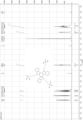
- FIG. 2 is a 1 HNMR chart of the compounds produced in Examples.
- FIG. 3 is a 1 HNMR chart of another compound produced in Examples.
- FIG. 4 is a 1 HNMR chart of still another compound produced in Examples.
- FIG. 5 is a 1 HNMR chart of still another compound produced in Examples.
- FIG. 6 is a 1 HNMR chart of still another compound produced in Examples.
- FIG. 7 is a 1 HNMR chart of still another compound produced in Examples.
- FIG. 8 is a 1 HNMR chart of still another compound produced in Examples.
- photoelectric conversion element of the present invention includes both “first photoelectric conversion element of the present invention” and “second photoelectric conversion element of the present invention” unless otherwise specified.
- the hole transport layer may contain a compound represented by the following chemical formula (I).
- Ar 1 is a structure containing an aromatic ring, and may or may not contain a heteroatom in the atoms constituting the aromatic ring, Ar 1 may or may not have a substituent other than -L 1 -X 1 , -L 1 -X 1 may be one or more, and when there are more than one, each L 1 and each X 1 may be the same or different, each L 1 is an atomic group or a covalent bond connecting Ar 1 and X 1 ; Each X1 is a group capable of transferring charge to and from the first electrode.
- the number of -L 1 -X 1 is not particularly limited, but may range from 1 to 4, for example.
- Ar 1 in chemical formula (I) may be represented by chemical formula (I-1) below.
- Ar 11 is an atomic group containing a cyclic structure, and the cyclic structure may be either an aromatic ring or a non-aromatic ring, and may be a monocyclic ring, a condensed ring, or a spiro ring.
- Ar 12 is an aromatic ring, which may or may not contain a heteroatom among the atoms constituting the ring;
- Ar 12 may be united with Ar 11 by sharing one or more atoms with Ar 11 ;
- Ar 12 may be one or more, and when there are more than one, they may be the same or different.
- the number of Ar 12 is not particularly limited, but may range from 1 to 4, for example.
- the Ar 11 may be represented by any one of the following chemical formulas (a1) to (a10).
- each Ar 12 in the chemical formula (I-1) may be represented by the following chemical formula (b).
- the carbon atoms C 1 and C 2 also serve as part of the atoms constituting the ring structure of Ar 11 in the chemical formula (I-1),
- the R 1 is a hydrogen atom, X 1 in the chemical formula (I), or a substituent, the substituent may or may not contain a hydrogen atom, and the hydrogen atom in the substituent at least one of may be substituted with X 1 in the chemical formula (I),
- Each R 11 may be the same or different, and each is a hydrogen atom or a substituent, or two adjacent R 11 are combined with the benzene ring to which they are bonded to form a condensed ring. may be
- Each R 11 may or may not have a further substituent.
- the chemical formula (b) may be represented by any one of the following chemical formulas (b1) to (b7).
- the compound represented by the chemical formula (I) may be a compound represented by any one of the following chemical formulas A-1 to A-23.
- Each R 1 is a hydrogen atom, X 1 in the chemical formula (I), or a substituent further substituted with X 1 in the chemical formula (I), and the same but can be different, at least one of the R 1 is X 1 in the chemical formula (I) or a substituent further substituted with X 1 in the chemical formula (I);
- the R 2 is a substituent, and may be one or more, or may not be present, and when there are multiple, each R 2 may be the same or different.
- R 1 when R 1 is a substituent further substituted with X 1 in the chemical formula (I), the number of X 1 may be 1 or plural. Further, when R 1 is a substituent further substituted by X 1 in the chemical formula (I), it is, for example, an alkyl group or an alkoxy group further substituted by X 1 in the chemical formula (I). may
- substituents R 2 are not particularly limited.
- the substituents R 2 may also be, for example, alkyl groups, alkoxy groups, or halo groups (halogen atoms), respectively.
- the compound represented by the chemical formula (I) has the following chemical formulas 4PATAT, 1-legged-3PATAT, 1-legged-3PATAT-H, 2-legged-3PATAT, 4PATTI-C3, Or it may be a compound represented by 4PATTI-C4.
- the hole transport layer may further contain a co-adsorbent.
- the co-adsorbent may be a compound represented by the following chemical formula (II).
- L 2 is an alkyl group, an alkoxy group, an aryl group, or a heterocyclic ring, at least one hydrogen atom of L 2 is substituted with X 2 , and it has a substituent other than X 2 may or may not have X 2 is a group capable of transferring charge to and from the first electrode, and may be one or more, and if there are more than one, they may be the same or different.
- the co-adsorbent may have a molecular weight of 2,000 or less.
- the photoelectric conversion layer may contain an organic-inorganic perovskite compound.
- the organic-inorganic perovskite compound may contain at least one of tin and lead.
- the photoelectric conversion element of the present invention may be, for example, a solar cell.
- the number of -L 1 -X 1 in the chemical formula (I) may be in the range of 1-4.
- Ar 1 may be represented by the following chemical formula (I-1).
- Ar 11 is an atomic group containing a cyclic structure, and the cyclic structure may be either an aromatic ring or a non-aromatic ring, and may be a monocyclic ring, a condensed ring, or a spiro ring.
- Ar 12 is an aromatic ring, which may or may not contain a heteroatom among the atoms constituting the ring;
- Ar 12 may be united with Ar 11 by sharing one or more atoms with Ar 11 ;
- Ar 12 may be one or more, and when there are more than one, they may be the same or different.
- the number of Ar 12 is not particularly limited, but may range from 1 to 4, for example.
- Ar 11 may be represented by any one of the following chemical formulas (a1) to (a10).
- each Ar 12 may be represented by the following chemical formula (b).
- the carbon atoms C 1 and C 2 also serve as part of the atoms constituting the ring structure of Ar 11 in the chemical formula (I-1),
- the R 1 is a hydrogen atom, X 1 in the chemical formula (I), or a substituent, the substituent may or may not contain a hydrogen atom, and the hydrogen atom in the substituent at least one of may be substituted with X 1 in the chemical formula (I),
- Each R 11 may be the same or different, and each is a hydrogen atom or a substituent, or two adjacent R 11 are combined with the benzene ring to which they are bonded to form a condensed ring. may be
- Each R 11 may or may not have a further substituent.
- the chemical formula (b) may be represented by any one of the following chemical formulas (b1) to (b7).
- the compound represented by the chemical formula (I) may be a compound represented by any one of the following chemical formulas A-1 to A-23.
- Each R 1 is a hydrogen atom, X 1 in the chemical formula (I), or a substituent further substituted with X 1 in the chemical formula (I), and the same but can be different, at least one of the R 1 is X 1 in the chemical formula (I) or a substituent further substituted with X 1 in the chemical formula (I);
- the R 2 is a substituent, and may be one or more, or may not be present, and when there are multiple, each R 2 may be the same or different.
- R 1 when R 1 is a substituent further substituted with X 1 in the chemical formula (I), the number of X 1 may be 1 or plural. Further, when R 1 is a substituent further substituted by X 1 in the chemical formula (I), it is, for example, an alkyl group or an alkoxy group further substituted by X 1 in the chemical formula (I). may
- substituents R 2 are not particularly limited.
- the substituents R 2 may also be, for example, alkyl groups, alkoxy groups, or halo groups (halogen atoms), respectively.
- the compound represented by the chemical formula (I) is a compound represented by the following chemical formula 4PATAT, 1-legged-3PATAT, 1-legged-3PATAT-H, 2-legged-3PATAT, 4PATTI-C3, or 4PATTI-C4 There may be.
- X 1 in the chemical formula (I) is at least one hydrogen of a group capable of transferring charge to and from an electrode instead of a group capable of transferring charge to and from an electrode. It may be a group in which atoms are substituted with further substituents.
- the substituents may be, for example, alkyl groups or halogen atoms, and if there are multiple substituents, they may be the same or different.
- each R in each X 1 is a substituent, and when there are a plurality of them, they may be the same or different.
- each of the substituents R in each X 1 in the chemical formula (I) may be, for example, an alkyl group or a halogen atom.
- the compound represented by the chemical formula (I) is the following chemical formula 4PAE-TAT, 1-legged-3PAE-TAT-H, 1-legged-3PAEE-TAT, 2-legged-3PAH-TAT, 4PATTI-C3, or 4PATTI It may be a compound represented by -C4.
- a chain group or atomic group e.g., a hydrocarbon group such as an alkyl group or an unsaturated aliphatic hydrocarbon group
- a hydrocarbon group such as an alkyl group or an unsaturated aliphatic hydrocarbon group
- a chain group or atomic group may be linear or branched, unless otherwise specified. is not particularly limited, but is, for example, 1 to 40, 1 to 32, 1 to 24, 1 to 18, 1 to 12, 1 to 6, or 1 to 2 (2 or more in the case of an unsaturated hydrocarbon group). It can be.
- the number of ring members (the number of atoms constituting the ring) of a cyclic group or atomic group is For example, without limitation, it may be 5-32, 5-24, 6-18, 6-12, or 6-10.
- any isomers may be used unless otherwise specified.
- simply referred to as a "naphthyl group” may be a 1-naphthyl group or a 2-naphthyl group.
- the "substituent” is not particularly limited, but examples include alkyl groups, unsaturated aliphatic hydrocarbon groups, alkoxy groups, aralkyl groups, aryl groups, heteroaryl groups, halogens, hydroxy groups (--OH), A mercapto group (-SH), an alkylthio group (-SR, R is an alkyl group), a sulfo group, a nitro group, a diazo group, a cyano group, a trifluoromethyl group and the like.
- any isomer Bodies can also be used in the present invention.
- the salt when a compound can form a salt, the salt can also be used in the present invention unless otherwise specified.
- the salt may be an acid addition salt or a base addition salt.
- the acid forming the acid addition salt may be an inorganic acid or an organic acid
- the base forming the base addition salt may be an inorganic base or an organic base.
- inorganic acid examples include, but are not limited to, sulfuric acid, phosphoric acid, hydrofluoric acid, hydrochloric acid, hydrobromic acid, hydroiodic acid, hypofluorous acid, hypochlorous acid, hypobromous acid, Hypoiodous acid, fluorous acid, chlorous acid, bromous acid, iodous acid, fluoric acid, chloric acid, bromic acid, iodic acid, perfluoric acid, perchloric acid, perbromic acid, periodic acid, etc. is given.
- the organic acid is also not particularly limited, but examples thereof include p-toluenesulfonic acid, methanesulfonic acid, oxalic acid, p-bromobenzenesulfonic acid, carbonic acid, succinic acid, citric acid, benzoic acid and acetic acid.
- the inorganic base include, but are not limited to, ammonium hydroxide, alkali metal hydroxide, alkaline earth metal hydroxide, carbonate and hydrogen carbonate. Examples include sodium hydroxide, potassium hydroxide, potassium carbonate, sodium carbonate, sodium hydrogen carbonate, potassium hydrogen carbonate, calcium hydroxide and calcium carbonate.
- the organic base is also not particularly limited, and examples thereof include ethanolamine, triethylamine and tris(hydroxymethyl)aminomethane.
- the method for producing these salts is not particularly limited, either, and they can be produced, for example, by adding an acid or base as described above to the above compounds as appropriate by a known method.
- the first photoelectric conversion element of the present invention is The first electrode, the hole transport layer, the photoelectric conversion layer, the electron transport layer, and the second electrode are laminated in the order,
- the photoelectric conversion layer includes a perovskite structure,
- the hole transport layer has an ionization potential in the range of -5.4 eV to -5.7 eV.
- the second photoelectric conversion element of the present invention is The first electrode, the hole transport layer, the photoelectric conversion layer, the electron transport layer, and the second electrode are laminated in the order,
- the photoelectric conversion layer includes a perovskite structure,
- the hole transport layer is characterized by containing a compound represented by the following chemical formula (I).
- Ar 1 , L 1 and X 1 in the following chemical formula (I) are as described above.
- the number of -L 1 -X 1 is not particularly limited, but may range from 1 to 4, for example.
- the first electrode, the hole transport layer, the photoelectric conversion layer, the electron transport layer, and the second electrode are laminated in the order described above.
- the photoelectric conversion element of the present invention may contain other components other than the first electrode, the hole transport layer, the photoelectric conversion layer, the electron transport layer, and the second electrode, It does not have to be included.
- the first electrode and the hole transport layer may be directly laminated without any other component between them, or may be laminated with other component between them. good too.
- the hole-transporting layer and the photoelectric conversion layer may be directly laminated without any other constituents between them, or may be laminated with other constituents between them. good too.
- the photoelectric conversion layer and the electron-transporting layer may be directly laminated without any other component between them, or may be laminated with another component between them. good.
- the electron-transporting layer and the second electrode may be directly laminated with no other constituents between them, or may be laminated with other constituents between them. good too.
- Each component in the photoelectric conversion device of the present invention has an ionization potential of the hole transport layer in the range of ⁇ 5.4 eV to ⁇ 5.7 eV (first photoelectric conversion device of the present invention), or
- the hole transport layer is not particularly limited except that it contains the compound represented by the chemical formula (I) (the second photoelectric conversion device of the present invention). It may be the same as or conforming to the recommended battery).
- the hole transport layer is not particularly limited except that the ionization potential is ⁇ 5.4 eV to ⁇ 5.7 eV. It may or may not contain a compound that
- the hole transport layer is not particularly limited except that it contains the compound represented by the chemical formula (I). It may be within the range of 0.7 eV or may be outside the range.
- the photoelectric conversion element of the present invention is not limited to the following examples.
- the case where the photoelectric conversion element of this invention is a solar cell is mainly demonstrated below.
- the photoelectric conversion element 10 includes a support (also referred to as a substrate, base material, etc.) 11, a first electrode 12, a hole transport layer 13, a photoelectric conversion layer 14, an electron transport layer 15, and a second Two electrodes 16 are stacked in the order described above.
- the support 11 is not particularly limited, and for example, a substrate that can be used for a general photoelectric conversion element such as a solar cell may be appropriately used.
- the substrate include glass, plastic plates, plastic films, inorganic crystals, and the like.
- Substrates having at least one film selected from a metal film, a semiconductor film, a conductive film and an insulating film formed on part or all of the surface of these substrates can also be suitably used as the support 11. can be done.
- the size, thickness, etc. of the support 11 are also not particularly limited, and may be, for example, similar to or conforming to general photoelectric conversion elements such as solar cells.
- the first electrode 12 is, for example, a layer that supports the hole transport layer 13 and has a function of extracting holes from the photoelectric conversion layer 14 .
- the first electrode 12 is, for example, a layer that functions as a cathode (positive electrode).
- the first electrode 12 may be formed directly on the support 11, for example.
- the first electrode 12 may be, for example, a transparent electrode made of a conductor.
- the transparent electrode is not particularly limited, examples thereof include tin-doped indium oxide (ITO) film, impurity-doped indium oxide (In 2 O 3 ) film, impurity-doped zinc oxide (ZnO) film, fluorine-doped tin dioxide ( FTO) film, a laminated film formed by laminating two or more of these, gold, silver, copper, aluminum, tungsten, titanium, chromium, nickel, cobalt, and the like. These may be used singly or as a mixture of two or more, and may be a single layer or a laminate.
- These films may also function, for example, as anti-diffusion layers.
- the thickness of the first electrode 12 is not particularly limited, it is preferably adjusted so that the sheet resistance is 5 to 15 ⁇ / ⁇ (per unit area), for example.
- the method for forming the first electrode 12 is not particularly limited, for example, it can be obtained by a known film forming method depending on the material to be formed.
- the shape of the first electrode 12 is not particularly limited.
- the method for forming the first electrode 12 on the support 11 is not particularly limited, for example, a known method may be used, and vacuum deposition such as vacuum deposition or sputtering is preferred. A patterned one may be used as the first electrode 12 .
- the patterning method is not limited to two, but includes, for example, a method of immersing in a laser or an etching solution, a method of patterning using a mask during vacuum film formation, etc. Any method may be used in the present invention.
- the first electrode 12 may be used together with a metal wiring or the like for the purpose of lowering the electrical resistance value.
- the material of the metal wiring is not particularly limited, but examples thereof include aluminum, copper, silver, gold, platinum and nickel.
- the metal lead wire can be used in combination by forming the metal lead wire on the first substrate by, for example, vapor deposition, sputtering, pressure bonding, etc., and providing a layer of ITO or FTO thereon, or providing it on ITO or FTO. be.
- the hole transport layer 13 has an ionization potential in the range of ⁇ 5.4 eV to ⁇ 5.7 eV (the first photoelectric conversion element of the present invention), or is represented by the chemical formula (I) (second photoelectric conversion element of the present invention).
- the hole transport layer 13 is not particularly limited, and may be, for example, similar to or conforming to the hole transport layer of a general photoelectric conversion element (for example, a general battery).
- the ionization potential of the hole-transport layer 13 is ⁇ 5.4 eV.
- the ionization potential of the hole transport layer 13 is ⁇ 5.7 eV or higher. Preferably.
- the compound represented by the chemical formula (I) can be used.
- the chemical formula (I) is, for example, as described above.
- L 1 in the chemical formula (I) include, in addition to the above, a divalent alkylene group such as a 1,1-methylene group and a 1,2-ethylene group, and a divalent group such as diethoxyethane. and the like, which may or may not have substituents other than X 1 .
- a phosphonic acid group, a trihalogenated silyl group, and a trialkoxysilyl group are preferable from the viewpoint of being able to bond firmly with the first electrode 12 (for example, a transparent electrode).
- the compound represented by the chemical formula (I) can be used, for example, as a hole transport compound that forms a monomolecular layer on the transparent conductive film.
- the transparent conductive film is, for example, the first electrode that is a transparent electrode, and the transparent electrode is, for example, ITO or the like as described above.
- the compound represented by the chemical formula (I) has an ionization potential of ⁇ 5.4 eV or less, so that it is difficult to react with oxygen and a device (element) can be stably produced. A highly durable photoelectric conversion element can be obtained.
- the method for forming the hole transport layer 13 is not particularly limited. can be formed.
- the method of adsorbing the compound represented by the chemical formula (I) to the first electrode 12 to form a monomolecular layer is not particularly limited, but for example, the compound represented by the chemical formula (I) is dissolved in a solvent and then contact and bond with the first electrode 12 .
- the bond between the compound represented by the chemical formula (I) and the first electrode 12 is not particularly limited, and may be a physical bond or a chemical bond.
- the type of the bond is also not particularly limited, and may be, for example, a hydrogen bond, an ester bond, a chelate bond, or the like.
- the solvent for dissolving the compound represented by the chemical formula (I) is also not particularly limited, and may be either or both of water and an organic solvent.
- the solvent include, more specifically, water, alcohols such as methanol, ethanol and 2-propanol, ethers such as diethyl ether and diisopropyl ether, ketones such as acetone and methyl isobutyl ketone, ethyl acetate, esters such as isobutyl acetate and ⁇ -butyrolactone; heterocycles such as tetrahydrofuran and thiophene; amides such as N,N-dimethylformamide, N,N-dimethylacetamide and N-methylpyrrolidone; sulfoxides such as dimethylsulfoxide; Sulfones such as diethylsulfone and sulfolane; Nitriles such as acetonitrile and 3-methoxypropionitrile; Aromatic compounds such as benz
- a specific method for forming a monomolecular layer by adsorbing the compound represented by the chemical formula (I) on the first electrode 12 is not particularly limited, but examples include dipping, spraying, spin coating, A known method such as a bar coat method can be used.
- the temperature during adsorption is not particularly limited, but is preferably -20°C to 100°C, more preferably 0°C to 50°C.
- the adsorption time is also not particularly limited, but is preferably 1 second to 48 hours, more preferably 10 seconds to 1 hour.
- washing may or may not be performed.
- the washing method is also not particularly limited, and for example, a known method may be used as appropriate.
- Heat treatment may or may not be performed after the adsorption treatment or after the washing.
- the temperature of the heat treatment is preferably 50°C to 150°C, more preferably 70°C to 120°C.
- the heat treatment time is preferably 1 second to 48 hours, more preferably 10 seconds to 1 hour. Moreover, this heat treatment may be performed in the air or in a vacuum, for example.
- a co-adsorbent When the compound represented by the chemical formula (I) is adsorbed on the first electrode 12, for example, a co-adsorbent may be used together, or may not be used together.
- the co-adsorbent is added for the purpose of, for example, when the compound represented by the chemical formula (I) alone cannot completely cover the electrode surface, or for the purpose of inhibiting the interaction between the compounds represented by the chemical formula (I). can do.
- the coadsorbent is not particularly limited, for example, as described above, the compound represented by the chemical formula (II) can be used.
- the L 2 and X 2 in the chemical formula (II) are, for example, as described above.
- Specific examples of the compound represented by the chemical formula (II) are not particularly limited, but for example, n-butylphosphonic acid, n-hexylphosphonic acid, n-decylphosphonic acid, n-octadecylphosphonic acid, 2-ethylhexyl Phosphonic acid compounds such as phosphonic acid, methoxymethylphosphonic acid, 3-acryloyloxypropylphosphonic acid, 11-hydroxyundecylphosphonic acid, 1H,1H,2H,2H-perfluorophosphonic acid, acetic acid, propionic acid, isobutyric acid, nonane acid, fluoroacetic acid, ⁇ -chloropropionic acid, glyoxylic acid, etc., and these may be used alone or in combination of two or more.
- the molecular weight of the compound represented by the chemical formula (II) is not particularly limited. may be The smaller the molecular weight, the higher the coverage when forming a layer on the electrode (for example, ITO), so the smaller the molecular weight, the better.
- the method of adsorbing the co-adsorbent to the first electrode 12 is not particularly limited, but a method of dissolving it in a solvent and then adsorbing it is preferable, as in the case of the compound represented by the chemical formula (I).
- the solvent is also not particularly limited, but may be, for example, the same solvents as those exemplified above for the compound represented by the chemical formula (I).
- the co-adsorbent may be adsorbed by immersing the first electrode 12 in a solvent in which the co-adsorbent is dissolved after the compound represented by the chemical formula (I) is once adsorbed on the substrate. , and the compound represented by the above chemical formula (I) may be mixed and dissolved in an organic solvent.
- the photoelectric conversion layer 14 is not particularly limited, and may be, for example, the same photoelectric conversion layer used in a general photoelectric conversion element such as a solar cell.
- the photoelectric conversion layer 14 contains, for example, a perovskite compound.
- the perovskite compound may be, for example, a compound represented by the following chemical formula (III). X ⁇ Y ⁇ Z ⁇ . . . (III)
- the ratio of ⁇ : ⁇ : ⁇ is 3:1:1, and ⁇ and ⁇ represent integers greater than 1.
- X represents a halogen ion
- Y represents an amino group-containing organic compound
- Z represents a metal ion.
- the perovskite layer is preferably positioned adjacent to the electron transport layer. Note that the ratio of ⁇ : ⁇ : ⁇ does not necessarily have to be 3:1:1, such as 3:1.05:0.95.
- X in the chemical formula (III) is not particularly limited and can be appropriately selected depending on the purpose.
- examples thereof include halogen ions such as chlorine, bromine, and iodine. These may be used individually by 1 type, and may use 2 or more types together.
- Y in the chemical formula (III) includes alkylamine compound ions (organic compounds having an amino group) such as methylamine, ethylamine, n-butylamine, and formamidine, and alkalis such as cesium, potassium, and rubidium, which are not limited to organic compounds.
- Metal ions are mentioned.
- the alkylamine compound ions and alkali metal ions may be used singly or in combination of two or more.
- Organic (alkylamine compound ions) and inorganic (alkali metal ions) can also be used in combination. For example, cesium ions and formamidine may be used in combination.
- Z in the chemical formula (III) is not particularly limited and can be appropriately selected according to the purpose.
- examples include metals such as lead, indium, antimony, tin, copper, and bismuth. These may be used individually by 1 type, and may use 2 or more types together. Especially lead Among them, combination of lead and tin is particularly preferable.
- the perovskite layer preferably exhibits a layered perovskite structure in which a layer composed of a metal halide and a layer in which organic cation molecules are arranged are alternately laminated.
- the perovskite layer may contain alkali metals. If the perovskite layer contains at least an alkali metal, it is advantageous in terms of high output.
- Alkali metals include, for example, cesium, rubidium, and potassium. Among these, cesium is preferred.
- the photoelectric conversion layer 14 may be a perovskite layer formed from a perovskite compound, as described above.
- the method for forming such a perovskite layer is not particularly limited and can be appropriately selected according to the purpose. A drying method and the like can be mentioned.
- a solution in which a metal halide is dissolved or dispersed is applied, dried, and then immersed in a solution in which an alkylamine halide is dissolved to form a perovskite compound.
- a stepwise precipitation method and the like can be mentioned.
- a poor solvent a solvent with low solubility
- a method of precipitating and the like can be mentioned.
- a perovskite layer includes, for example, a method of vapor-depositing a metal halide in a gas filled with methylamine or the like.
- a method for forming the perovskite layer a method of precipitating crystals by adding a poor solvent for the perovskite compound while applying a solution in which the metal halide and the alkylamine halide are dissolved or dispersed is particularly preferable.
- the method of applying these solutions is not particularly limited and can be appropriately selected depending on the purpose. be done.
- a method of applying the solution for example, a method of precipitating in a supercritical fluid using carbon dioxide or the like may be used.
- the poor solvent used includes hydrocarbons such as n-hexane and n-octane, alcohols such as methanol, ethanol and 2-propanol, diethyl ether, Ethers such as diisopropyl ether, ketones such as acetone and methyl isobutyl ketone, esters such as ethyl acetate, isobutyl acetate and ⁇ -butyrolactone, nitriles such as acetonitrile and 3-methoxypropionitrile, benzene, toluene, chlorobenzene, etc. aromatic hydrocarbon compounds, halogen-based solvents such as dichloromethane and chloroform, and fluorine-based solvents such as chlorofluorocarbons, hydrochlorofluorocarbons and hydrofluorocarbons.
- hydrocarbons such as n-hexane and n-octane
- alcohols such as methanol, ethanol and 2-prop
- the thickness of the photoelectric transport layer 14 is not particularly limited, but from the viewpoint of further suppressing performance deterioration due to defects and peeling, it is preferably 50 to 1200 nm, more preferably 200 to 600 nm. .
- the material used for the electron transport layer 15 is not particularly limited and can be appropriately selected depending on the purpose, but a semiconductor material is preferable.
- the semiconductor material is not particularly limited, and known materials can be used. Examples thereof include single semiconductors, compound semiconductors, organic n-type semiconductors, and the like.
- the single semiconductor is not particularly limited, but examples thereof include silicon and germanium.
- the compound semiconductor is not particularly limited, but for example, metal chalcogenides, specifically titanium, tin, zinc, iron, tungsten, zirconium, hafnium, strontium, indium, cerium, yttrium, lanthanum, vanadium, niobium, oxides such as tantalum; sulfides such as cadmium, zinc, lead, silver, antimony and bismuth; selenides such as cadmium and lead; tellurides such as cadmium; Other compound semiconductors include phosphides such as zinc, gallium, indium and cadmium, gallium arsenide, copper-indium-selenide and copper-indium-sulfide.
- organic n-type semiconductor examples include, but are not limited to, perylenetetracarboxylic anhydride, perylenetetracarboxydiimide compound, naphthalenediimide-bithiophene copolymer, benzobisimidazobenzophenanthroline polymer, C60, C70, PCBM ( [6,6]-phenyl-C 61 -butyric acid methyl ester), carbonyl bridge-bithiazole compounds, ALq3 (tris(8-quinolinolato)aluminum), triphenylene bipyridyl compounds, silole compounds, oxadiazole compounds, etc. can be mentioned.
- an organic n-type semiconductor is particularly preferable.
- the materials used for forming the electron transport layer 15 may be used singly or in combination of two or more.
- the crystal type of the semiconductor material is not particularly limited and can be appropriately selected according to the purpose, and may be single crystal, polycrystal, or amorphous.
- the thickness of the electron-transporting layer 15 is not particularly limited and can be appropriately selected according to the purpose.
- the method for forming the electron transport layer 15 is not particularly limited, and can be appropriately selected according to the purpose. Examples thereof include a method of forming a thin film in vacuum (vacuum film forming method), a wet film forming method, and the like.
- Vacuum film forming methods include, for example, a sputtering method, a pulse laser deposition method (PLD method), an ion beam sputtering method, an ion assist method, an ion plating method, a vacuum vapor deposition method, an atomic layer deposition method (ALD method), Chemical vapor deposition method (CVD method) etc. are mentioned.
- the wet film-forming method examples include a method of applying a solvent in which an electron-transporting material is dissolved, and a sol-gel method in the case of an oxide semiconductor.
- the sol-gel method is a method in which a gel is produced from a solution through chemical reactions such as hydrolysis and polymerization/condensation, and then densification is promoted by heat treatment.
- the method of applying the sol solution is not particularly limited and can be appropriately selected depending on the purpose.
- method, blade coating method, gravure coating method, and wet printing methods include letterpress, offset, gravure, intaglio, rubber plate, screen printing and the like.
- the temperature for the heat treatment after applying the sol solution is preferably 80° C. or higher, more preferably 100° C. or higher.
- An electron injection layer may be formed between the electron transport layer 15 and the second electrode 16 after forming the electron transport layer 15 .
- BCP bathoproine
- the thickness of the electron injection layer is preferably 1 nm to 100 nm, more preferably 3 nm to 20 nm.
- the second electrode 16 (which may be, for example, a back electrode) is a layer having a function of extracting electrons from the photoelectric conversion layer 14 via an electron transport layer, for example. Also, the second electrode 16 is a layer that functions as an anode (negative electrode), for example.
- the second electrode 16 may be formed directly on the electron transport layer (also called electron injection layer) 15 .
- the material of the second electrode 16 is not particularly limited, and for example, the same material as that of the first electrode 12 can be used.
- the shape, structure, and size of the second electrode 16 are not particularly limited, and can be appropriately selected according to the purpose.
- Materials for the second electrode 16 include metals, carbon compounds, conductive metal oxides, and conductive polymers.
- Examples of the metal include platinum, gold, silver, copper, and aluminum.
- Examples of the carbon compound include graphite, fullerene, carbon nanotube, and graphene.
- Examples of the conductive metal oxide include ITO, FTO, and ATO.
- Examples of the conductive polymer include polythiophene and polyaniline.
- the materials used for forming the second electrode 16 may be used singly or in combination of two or more.
- the second electrode 16 can be appropriately formed on the electron transport layer 15 by using a method such as coating, lamination, vacuum deposition, CVD, or bonding depending on the type of material used and the type of the hole transport layer 13. be.
- At least one of the first electrode 12 and the second electrode 16 is preferably substantially transparent.
- the electrodes transparent and allow incident light to enter from the electrode side.
- a material that reflects light for the back electrode such as metal, glass deposited with a conductive oxide, or plastic.
- a metal thin film, and the like are preferably used. It is also effective to provide an antireflection layer on the electrode on the incident light side.
- the configuration of the photoelectric conversion element of the present invention is not limited to the configuration of FIG.
- the support 11 is arranged on the side opposite to that in FIG. Layer 14, hole transport layer 13, and first electrode 12 may be stacked in the order described above.
- other constituent elements are provided between the layers of the support 11, the first electrode 12, the hole transport layer 13, the photoelectric conversion layer 14, the electron transport layer 15, and the second electrode 16. It may or may not exist.
- the photoelectric conversion element of the present invention is not limited to this.
- the first electrode may be the back electrode and the second electrode may be the transparent electrode.
- the photoelectric conversion element of the present invention (for example, a solar cell) is preferably sealed to protect the device (photoelectric conversion element of the present invention) from water and oxygen.
- the structure of the sealing is not particularly limited, it may be, for example, the same as that of a general photoelectric conversion element (for example, a solar cell). It may be coated and covered with glass or film, or the entire surface of the photoelectric conversion element of the present invention may be coated with the sealing material and covered with glass or film, or the entire surface of the photoelectric conversion element of the present invention may be covered with the sealing material. It may be applied only.
- the material of the sealing member is not particularly limited, and can be appropriately selected according to the purpose.
- epoxy resin or acrylic resin is preferably used and cured. It does not matter if only the coating is cured.
- the epoxy resin is not particularly limited, but includes, for example, water dispersion type, solventless type, solid type, heat curing type, curing agent mixed type, ultraviolet curing type, etc. Among them, thermosetting type and ultraviolet curing type is preferred, and an ultraviolet curable type is more preferred. It should be noted that even if it is an ultraviolet curing type, it is possible to heat, and it is preferable to heat even after ultraviolet curing.
- Specific examples of epoxy resins include bisphenol A type, bisphenol F type, novolac type, cycloaliphatic type, long chain aliphatic type, glycidylamine type, glycidyl ether type, glycidyl ester type, etc., and these can be used alone.
- Epoxy resin compositions that are already commercially available can be used in the present invention. Among others, there are epoxy resin compositions developed and marketed for use in solar cells and organic EL devices, which can be used particularly effectively in the present invention.
- epoxy resin compositions include, for example, TB3118, TB3114, TB3124, TB3125F (manufactured by ThreeBond Co., Ltd.), WorldRock5910, WorldRock5920, WorldRock8723 (manufactured by Kyoritsu Chemical Sangyo Co., Ltd.), WB90US(P), and WB90US-HV. (manufactured by Moresco) and the like.
- acrylic resin is not particularly limited, for example, those developed and commercially available for use in solar cells and organic EL elements can be effectively used.
- Commercially available acrylic resin compositions include, for example, TB3035B and TB3035C (manufactured by ThreeBond Co., Ltd.).
- the curing agent is not particularly limited and can be appropriately selected depending on the intended purpose. Examples thereof include amine-based, acid anhydride-based, polyamide-based and other curing agents.
- Amine-based curing agents include aliphatic polyamines such as diethylenetriamine and triethylenetetramine; aromatic polyamines such as metaphenylenediamine, diaminodiphenylmethane and diaminodiphenylsulfone; and acid anhydride-based curing agents include phthalic anhydride.
- curing agents include imidazoles and polymercaptans. These may be used alone or in combination of two or more.
- the additive is not particularly limited and can be appropriately selected depending on the intended purpose. agents, plasticizers, coloring agents, flame retardant aids, antioxidants, organic solvents, and the like. Among these, fillers, gap agents, curing accelerators, polymerization initiators, and desiccants (hygroscopic agents) are preferred, and fillers and polymerization initiators are more preferred.
- a filler as an additive, it suppresses the infiltration of moisture and oxygen, further reduces volume shrinkage during curing, reduces outgassing during curing or heating, improves mechanical strength, and thermal conductivity. and the control of fluidity can be obtained. Therefore, including a filler as an additive is very effective in maintaining stable output in various environments.
- the filler is not particularly limited and can be appropriately selected depending on the purpose. Examples include crystalline or amorphous silica, silicate minerals such as talc, alumina, aluminum nitride, silicon nitride, and calcium silicate. and inorganic fillers such as calcium carbonate. Among these, hydrotalcite is particularly preferred. Moreover, these may be used alone or in combination of two or more.
- the average primary particle size of the filler is not particularly limited, it is preferably 0.1 ⁇ m or more and 10 ⁇ m or less, more preferably 1 ⁇ m or more and 5 ⁇ m or less.
- the average primary particle size of the filler is within the above preferable range, the effect of suppressing penetration of moisture and oxygen can be sufficiently obtained, the viscosity becomes appropriate, the adhesion to the substrate and the defoaming property are improved. It is also effective for controlling the width of the sealing portion and workability.
- the content of the filler is preferably 10 parts by mass or more and 90 parts by mass or less, more preferably 20 parts by mass or more and 70 parts by mass or less, relative to the entire sealing member (100 parts by mass).
- the content of the filler is within the above preferable range, the effect of suppressing penetration of moisture and oxygen is sufficiently obtained, the viscosity becomes appropriate, and the adhesion and workability become good.
- the gap agent is also called a gap control agent or a spacer agent.
- the gap material By including the gap material as an additive, it becomes possible to control the gap of the seal. For example, when a sealing member is provided on the first substrate or the first electrode, and the second substrate is placed thereon for sealing, the sealing member must be mixed with a gap agent. As a result, the gap of the sealing portion is aligned with the size of the gap agent, so that the gap of the sealing portion can be easily controlled.
- the gap agent is not particularly limited, for example, one that is granular, has a uniform particle size, and has high solvent resistance and heat resistance is preferable, and can be appropriately selected according to the purpose.
- the gap agent preferably has a high affinity with epoxy resin and has a spherical particle shape. Specifically, glass beads, silica fine particles, organic resin fine particles and the like are preferable. These may be used individually by 1 type, and may use 2 or more types together.
- the particle diameter of the gap agent can be selected according to the gap of the sealing portion to be set, but is preferably 1 ⁇ m or more and 100 ⁇ m or less, more preferably 5 ⁇ m or more and 50 ⁇ m or less.
- the polymerization initiator is not particularly limited, but includes, for example, a polymerization initiator that initiates polymerization using heat or light, and can be appropriately selected depending on the purpose.
- a polymerization initiator and the like are included.
- Thermal polymerization initiators are compounds that generate active species such as radicals and cations by heating, and include azo compounds such as 2,2'-azobisbutyronitrile (AIBN) and benzoyl peroxide (BPO). Examples include peroxides.
- a benzenesulfonic acid ester, an alkylsulfonium salt, or the like is used as the thermal cationic polymerization initiator.
- a photocationic polymerization initiator is preferably used in the case of an epoxy resin.
- a cationic photopolymerization initiator is mixed with an epoxy resin and irradiated with light, the cationic photopolymerization initiator decomposes to generate an acid, which causes polymerization of the epoxy resin and a curing reaction proceeds.
- a photocationic polymerization initiator has effects such as little volume shrinkage during curing, no oxygen inhibition, and high storage stability.
- photocationic polymerization initiator examples include aromatic diazonium salts, aromatic iodonium salts, aromatic sulfonium salts, metacelone compounds, and silanol/aluminum complexes.
- a photoacid generator having a function of generating an acid upon irradiation with light can also be used as the polymerization initiator.
- the photoacid generator acts as an acid that initiates cationic polymerization, and includes ionic sulfonium salt-based and iodonium salt-based onium salts composed of a cation portion and an anion portion. These may be used alone or in combination of two or more.
- the amount of the polymerization initiator added is not particularly limited and may vary depending on the material used, but is preferably 0.5 parts by mass or more and 10 parts by mass or less with respect to the entire sealing member (100 parts by mass). 1 part by mass or more and 5 parts by mass or less is more preferable.
- the desiccant (also referred to as a hygroscopic agent) is a material that has the function of physically or chemically adsorbing and absorbing moisture. can be reduced.
- the desiccant is not particularly limited and can be appropriately selected depending on the purpose, but is preferably particulate, such as calcium oxide, barium oxide, magnesium oxide, magnesium sulfate, sodium sulfate, calcium chloride. , silica gel, molecular sieves, and zeolites. Among these, zeolites with high moisture absorption are preferred. These may be used alone or in combination of two or more.
- the curing accelerator (also called a curing catalyst) is a material that accelerates the curing speed, and is mainly used for thermosetting epoxy resins.
- the curing accelerator is not particularly limited and can be appropriately selected depending on the intended purpose.
- -tertiary amines or tertiary amine salts such as diazabicyclo(4,3,0)-nonene-5
- imidazoles such as 1-cyanoethyl-2-ethyl-4-methylimidazole and 2-ethyl-4-methylimidazole
- phosphines such as triphenylphosphine and tetraphenylphosphonium/tetraphenylborate
- phosphonium salts may be used alone or in combination of two or more.
- the coupling agent is not particularly limited as long as it is a material that has the effect of increasing molecular bonding strength, and can be appropriately selected according to the purpose.
- Examples include silane coupling agents. Specifically, 3-glycidoxypropyltrimethoxysilane, 3-glycidoxypropylmethyldimethoxysilane, 3-glycidoxypropylmethyldimethoxysilane, 2-(3,4-epoxycyclohexyl)ethyltrimethoxysilane, N-phenyl- ⁇ -aminopropyltrimethoxysilane, N-(2-aminoethyl)3-aminopropylmethyldimethoxysilane, N-(2-aminoethyl)3-aminopropylmethyltrimethoxysilane, 3-aminopropyltrimethoxysilane Silane cups such as ethoxysilane, 3-mercaptopropyltrimethoxysilane, vinyltrime
- a sheet adhesive can be used.
- the sheet adhesive is, for example, a sheet on which a resin layer is formed in advance, and the sheet can be made of glass, a film having a high gas barrier property, or the like. Also, the sheet may be formed only from the sealing resin. It is also possible to apply a sheet adhesive onto the sealing film. It is also possible to form a structure in which a hollow portion is provided on the sealing film and then attach it to the device.
- the photoelectric conversion device is arranged so as to face the support.
- the shape, structure, size and type of the sealing film base material are not particularly limited and can be appropriately selected according to the purpose.
- the sealing film forms a barrier layer that prevents passage of moisture and oxygen on the surface of the base material, and may be formed on only one side or both sides of the base material.
- the barrier layer may be composed of a material containing, for example, a metal oxide, a metal, a mixture formed of a polymer and a metal alkoxide, or the like as a main component.
- the metal oxide include aluminum oxide, silicon oxide, aluminum, and the like.
- the polymer include polyvinyl alcohol, polyvinylpyrrolidone, methylcellulose, and the like. Examples include tetraethoxysilane, triisopropoxyaluminum, 3-glycidoxypropyltrimethoxysilane, 3-mercaptopropyltrimethoxysilane, 3-isocyanatopropyltriethoxysilane and the like.
- the barrier layer may be transparent or opaque, for example. Moreover, the barrier layer may be a single layer made of a combination of the above materials, or may be a multi-layered structure.
- a method for forming the barrier layer known methods can be used, and coating methods such as vacuum film formation such as sputtering, dipping, roll coating, screen printing, spraying, and gravure printing can be used. can.
- the photoelectric conversion element for example, a solar cell
- Lead wires are connected to the first electrode and the second electrode using a conductive material such as solder, silver paste, or graphite, for example.
- the conductive material may be used singly or in a mixed or laminated structure of two or more.
- the part where the lead wire is attached may be covered with an acrylic resin or an epoxy resin.
- a lead wire is a general term for electric wires for electrically connecting power supplies and electronic components in an electric circuit, and examples include vinyl wires and enameled wires.
- the application and method of use of the photoelectric conversion device of the present invention are not particularly limited, and for example, it can be widely used in the same applications as general photoelectric conversion devices (for example, general solar cells).
- the photoelectric conversion element (for example, a solar cell) of the present invention can be applied to a power supply device, for example, by combining it with a circuit board or the like that controls the generated current.
- Devices that use power supply devices include, for example, electronic desk calculators and solar radio-controlled wristwatches.
- auxiliary power supply for extending the continuous use time of rechargeable or dry battery electric appliances, or a secondary battery. It can also be used as an independent power supply that does not require battery replacement or power supply wiring.
- the yield (%) is the yield (mol%) based on the amount of substance (mol) unless otherwise specified.
- NMR (nuclear magnetic resonance) spectra were measured using AV400M manufactured by Bruker.
- Example A1 Synthesis of 4-PATAT
- 4-PATAT which is one of the compounds of the present invention (compounds represented by the above chemical formula (I))
- Example A2 Synthesis of 1-legged-3PATAT]
- 1-legged-3PATAT which is one of the compounds of the present invention (compounds represented by the above chemical formula (I))
- 1-legged-3PAE-TAT (215 mg), ethyl iodide (0.141 mg), and DMF (4.1 mL) were placed in a three-necked flask, and sodium hydride (43.4 mg) was added under an argon gas stream at room temperature while stirring. was added slowly. Stirring was continued for 1.5 hours, water was added to stop the reaction, and the mixture was extracted with ethyl acetate. After drying with sodium sulfate, the solvent was distilled off. The residue was purified by silica gel column chromatography (eluent: toluene) to obtain 147 mg of brown oily 1-legged-3PAEE-TAT (see the chemical formula in Scheme 5 above). The yield was 63% based on the starting 1-legged-3PAE-TAT.
- 1-legged-3PAEE-TAT 115 mg
- dichloromethane 5.4 mL
- trimethylsilane bromide 0.10 mg
- methanol 3.6 mL
- Example A3 Synthesis of 1-legged-3PATAT-H]
- 1-legged-3PATAT-H which is one of the compounds of the present invention (the compound represented by the chemical formula (I))
- 2-legged-3PAH-TAT 47 mg
- dichloromethane 2.8 mL
- trimethylsilane bromide 0.124 mg
- TTI 23.0 mg, 50 mmol
- cesium carbonate 130 mg, 400 mmol
- tetrabutylammonium bromide 6.4 mg, 20 mmol
- tetrahydrofuran 1 ml
- diethyl(3-bromopropyl)phosphonate 58 mL
- 300 mmol was added, and the mixture was heated and stirred at 80° C. for 1 hour. After cooling to room temperature, the organic layer extracted with dichloromethane was dried over magnesium sulfate.
- the yellow oily mixture obtained by concentration under reduced pressure was purified by silica gel chromatography (eluent ethyl acetate:methanol 1:1 ⁇ 1:2) to give 47.5 mg (41 mmol, yield 81) of the target compound 1. %, yellow oil).
- TTI 23.0 g, 50 mmol
- cesium carbonate 130 mg, 400 mmol
- tetrabutylammonium bromide 6.4 mg, 20 mmol
- 1,4-dibromobutane 36 mL, 300 mmol
- water was added to stop the reaction, and the mixture was extracted with dichloromethane three times. The separated organic layer was dried over magnesium sulfate, and the solvent was distilled off under reduced pressure.
- Example 1 A solar cell, which is a photoelectric conversion element of the present invention, was produced (manufactured) in the following manner.
- C60 with a thickness of 20 nm (electron transport layer), bathocuproine (BCP, 8 nm) (electron injection layer), and Ag (100 nm) (second electrode) were formed by vacuum deposition to produce a photoelectric conversion device.
- BCP, 8 nm bathocuproine
- Ag 100 nm
- the photoelectric conversion characteristics of the sealed device produced in Example 1 were measured by a method conforming to JISC8913:1998 for measuring the output of silicon crystal solar cells.
- a solar simulator (SMO-250III model manufactured by Spectroscopy Instruments Co., Ltd.) combined with an air mass filter equivalent to AM 1.5G was used as a light source for measurement by adjusting the light intensity to 100 mW/cm 2 with a secondary reference Si solar cell, and using a perovskite solar cell.
- the IV curve characteristics were measured using a source meter (manufactured by Keithley Instruments Inc., model 2400 general-purpose source meter).
- the short-circuit current (Isc), open-circuit voltage (Voc), fill factor (FF), short-circuit current density (Jsc), and photoelectric conversion efficiency (PCE) obtained from the V-curve characteristic measurement are expressed in the following equations 1 and 2. was calculated using The results are shown in Table 1 below. Also, this device was placed in a dryer at 85° C. in a dark place, and the photoelectric conversion efficiency was measured for 500 hours. The results are also shown in Table 1.
- Example 2 Example 1 except that the DMF solution of 4PATAT (0.1 mmol/L) in Example 1 was changed to a DMF solution of 4PATAT (0.1 mmol/L) and n-butylphosphonic acid (0.1 mmol/L). A photoelectric conversion element was produced (manufactured) in the same manner, and the photoelectric conversion efficiency was measured. The results are shown in Table 1 below. The IP (ionization potential) measured in the same manner as in Example 1 was -5.41 eV.
- Example 3 A photoelectric conversion element was produced in the same manner as in Example 1 except that the DMF solution of 4PATAT (0.1 mmol/L) in Example 1 was changed to a DMF solution of 1-legged-3PATAT (0.1 mmol/L) ( manufacturing), and the photoelectric conversion efficiency was measured. The results are shown in Table 1 below. The IP measured in the same manner as in Example 1 was -5.64 eV.
- Example 4 A photoelectric conversion element was produced in the same manner as in Example 1, except that the DMF solution of 4PATAT (0.1 mmol/L) in Example 1 was changed to a DMF solution of 1-legged-3PATAT-H (0.1 mmol/L). It was produced (manufactured) and the photoelectric conversion efficiency was measured. The results are shown in Table 1 below. The IP measured in the same manner as in Example 1 was -5.68 eV.
- Example 5 A photoelectric conversion element was produced in the same manner as in Example 1 except that the DMF solution of 4PATAT (0.1 mmol/L) in Example 1 was changed to the DMF solution of 2-legged-3PATAT (0.1 mmol/L) ( manufacturing), and the photoelectric conversion efficiency was measured. The results are shown in Table 1 below. The IP measured in the same manner as in Example 1 was -5.54 eV.
- Example 6 Except for changing the DMF solution of 4PATAT (0.1 mmol/L) in Example 1 to a DMF solution of 2-legged-3PATAT (0.1 mmol/L) and n-butylphosphonic acid (0.1 mmol/L) A photoelectric conversion element was produced (manufactured) in the same manner as in Example 1, and the photoelectric conversion efficiency was measured. The results are shown in Table 1 below. The IP measured in the same manner as in Example 1 was -5.50 eV.
- Example 7 Except for changing the DMF solution of 4PATAT (0.1 mmol/L) in Example 1 to a DMF solution of 1-legged-3PATAT (0.1 mmol/L) and n-butylphosphonic acid (0.1 mmol/L) A photoelectric conversion element was produced (manufactured) in the same manner as in Example 1, and the photoelectric conversion efficiency was measured. The results are shown in Table 1 below. The IP measured in the same manner as in Example 1 was -5.45 eV.
- Example 8 Example except that the DMF solution of 4PATAT (0.1 mmol/L) in Example 1 was changed to a DMF solution of 4PATTI-C3 (0.1 mmol/L) and n-butylphosphonic acid (0.1 mmol/L) A photoelectric conversion element was produced (manufactured) in the same manner as in 1, and the photoelectric conversion efficiency was measured. The results are shown in Table 2 below. Further, the IP (ionization potential) measured in the same manner as in Example 1 was ⁇ 5.57 eV.
- Example 9 Example except that the DMF solution of 4PATAT (0.1 mmol/L) in Example 1 was changed to a DMF solution of 4PATAT-C4 (0.1 mmol/L) and n-butylphosphonic acid (0.1 mmol/L) A photoelectric conversion element was produced (manufactured) in the same manner as in 1, and the photoelectric conversion efficiency was measured. The results are shown in Table 2 below.
- the IP (ionization potential) measured in the same manner as in Example 1 was -5.52 eV.
- Example 1 A photoelectric conversion element was produced in the same manner as in Example 1 except that the DMF solution of 4PATAT (0.1 mmol/L) in Example 1 was changed to a DMF solution of n-butylphosphonic acid (0.1 mmol/L) ( manufacturing), and the photoelectric conversion efficiency was measured. The results are shown in Table 1 below. The IP measured in the same manner as in Example 1 was -5.48 eV.
- Example 2 Example except that the DMF solution of 4PATAT (0.1 mmol/L) in Example 1 was changed to a DMF solution of [2-(9H-carbazol-9-yl)ethyl]phosphonic acid (0.1 mmol/L) A photoelectric conversion element was produced (manufactured) in the same manner as in 1, and the photoelectric conversion efficiency was measured. The results are shown in Table 1 below. Moreover, the ionization potential when this compound was adsorbed on the ITO substrate was -5.91 eV.
- Example 3 A DMF solution of 4PATAT (0.1 mmol/L) in Example 1 was added to a DMF solution of [2-(3,6-Dimethoxy-9H-carbazol-9-yl)ethyl]phosphonic Acid (0.1 mmol/L).
- a photoelectric conversion element was produced (manufactured) in the same manner as in Example 1, except for the change, and the photoelectric conversion efficiency was measured. The results are shown in Table 1 below. Also, the ionization potential when this compound was adsorbed on the ITO substrate was -5.25 eV.
- the photoelectric conversion device of the present invention is useful, for example, as a solar cell.
- the application and method of use of the photoelectric conversion device of the present invention are not particularly limited. be.
- the compound of the present invention for the hole transport layer of the photoelectric conversion device of the present invention for example, a photoelectric conversion device exhibiting excellent photoelectric conversion characteristics and having high durability can be obtained.
- the application and method of use of the compound of the present invention are not limited to this, and can be applied to any wide range of fields.
Landscapes
- Chemical & Material Sciences (AREA)
- Physics & Mathematics (AREA)
- Materials Engineering (AREA)
- Engineering & Computer Science (AREA)
- Electromagnetism (AREA)
- Spectroscopy & Molecular Physics (AREA)
- Inorganic Chemistry (AREA)
- Organic Chemistry (AREA)
- Health & Medical Sciences (AREA)
- Molecular Biology (AREA)
- General Health & Medical Sciences (AREA)
- Biochemistry (AREA)
- Life Sciences & Earth Sciences (AREA)
- Photovoltaic Devices (AREA)
- Electroluminescent Light Sources (AREA)
Priority Applications (7)
| Application Number | Priority Date | Filing Date | Title |
|---|---|---|---|
| JP2023546962A JP7575140B2 (ja) | 2021-09-13 | 2022-09-07 | 光電変換素子及び化合物 |
| EP22867372.9A EP4394845A4 (en) | 2021-09-13 | 2022-09-07 | PHOTOELECTRIC CONVERSION ELEMENT AND COMPOUND |
| US18/690,964 US20240389371A1 (en) | 2021-09-13 | 2022-09-07 | Photoelectric conversion element and compound |
| AU2022342541A AU2022342541A1 (en) | 2021-09-13 | 2022-09-07 | Photoelectric conversion element and compound |
| KR1020247010109A KR20240067896A (ko) | 2021-09-13 | 2022-09-07 | 광전 변환 소자 및 화합물 |
| CN202280061705.7A CN117981491A (zh) | 2021-09-13 | 2022-09-07 | 光电转换元件和化合物 |
| JP2024176979A JP2025014125A (ja) | 2021-09-13 | 2024-10-09 | 光電変換素子及び化合物 |
Applications Claiming Priority (2)
| Application Number | Priority Date | Filing Date | Title |
|---|---|---|---|
| JP2021-148447 | 2021-09-13 | ||
| JP2021148447 | 2021-09-13 |
Publications (1)
| Publication Number | Publication Date |
|---|---|
| WO2023038050A1 true WO2023038050A1 (ja) | 2023-03-16 |
Family
ID=85506352
Family Applications (1)
| Application Number | Title | Priority Date | Filing Date |
|---|---|---|---|
| PCT/JP2022/033514 Ceased WO2023038050A1 (ja) | 2021-09-13 | 2022-09-07 | 光電変換素子及び化合物 |
Country Status (7)
| Country | Link |
|---|---|
| US (1) | US20240389371A1 (https=) |
| EP (1) | EP4394845A4 (https=) |
| JP (2) | JP7575140B2 (https=) |
| KR (1) | KR20240067896A (https=) |
| CN (1) | CN117981491A (https=) |
| AU (1) | AU2022342541A1 (https=) |
| WO (1) | WO2023038050A1 (https=) |
Cited By (2)
| Publication number | Priority date | Publication date | Assignee | Title |
|---|---|---|---|---|
| CN116332994A (zh) * | 2023-02-24 | 2023-06-27 | 厦门大学 | 一种空穴传输材料及其合成方法和在钙钛矿太阳能电池的应用 |
| WO2024185793A1 (ja) * | 2023-03-06 | 2024-09-12 | 株式会社エネコートテクノロジーズ | 光電変換素子 |
Families Citing this family (3)
| Publication number | Priority date | Publication date | Assignee | Title |
|---|---|---|---|---|
| CN118388537B (zh) * | 2024-07-01 | 2024-12-06 | 天合光能股份有限公司 | 有机化合物及其制备方法与应用、钙钛矿太阳能电池 |
| CN119060095A (zh) * | 2024-07-23 | 2024-12-03 | 淮阴工学院 | 一种基于融噻吩并吲哚的自组装单分子膜空穴传输材料及其制备方法和应用 |
| CN121554509B (zh) * | 2026-01-21 | 2026-04-24 | 江苏盛开新能科技有限公司 | 一种三环稠和空穴传输材料、钙钛矿光伏器件及制备方法 |
Citations (2)
| Publication number | Priority date | Publication date | Assignee | Title |
|---|---|---|---|---|
| JP2021148447A (ja) | 2020-03-16 | 2021-09-27 | 株式会社東海理化電機製作所 | 位置検出装置 |
| JP2021174940A (ja) * | 2020-04-28 | 2021-11-01 | 三菱ケミカル株式会社 | 光電変換素子及び発電デバイス |
Family Cites Families (3)
| Publication number | Priority date | Publication date | Assignee | Title |
|---|---|---|---|---|
| CN110698654B (zh) * | 2018-07-10 | 2021-04-02 | 中国科学院长春应用化学研究所 | 基于三聚吲哚的超支化共轭聚电解质及其制备方法和用途 |
| CN109768170A (zh) * | 2019-01-23 | 2019-05-17 | 原秀玲 | 一种钙钛矿太阳能电池的制备方法 |
| KR102851579B1 (ko) * | 2020-02-24 | 2025-08-28 | 삼성디스플레이 주식회사 | 헤테로고리 화합물, 이를 포함한 유기 발광 소자 및 상기 유기 발광 소자를 포함한 전자 장치 |
-
2022
- 2022-09-07 JP JP2023546962A patent/JP7575140B2/ja active Active
- 2022-09-07 KR KR1020247010109A patent/KR20240067896A/ko active Pending
- 2022-09-07 US US18/690,964 patent/US20240389371A1/en active Pending
- 2022-09-07 CN CN202280061705.7A patent/CN117981491A/zh active Pending
- 2022-09-07 EP EP22867372.9A patent/EP4394845A4/en active Pending
- 2022-09-07 AU AU2022342541A patent/AU2022342541A1/en active Pending
- 2022-09-07 WO PCT/JP2022/033514 patent/WO2023038050A1/ja not_active Ceased
-
2024
- 2024-10-09 JP JP2024176979A patent/JP2025014125A/ja active Pending
Patent Citations (2)
| Publication number | Priority date | Publication date | Assignee | Title |
|---|---|---|---|---|
| JP2021148447A (ja) | 2020-03-16 | 2021-09-27 | 株式会社東海理化電機製作所 | 位置検出装置 |
| JP2021174940A (ja) * | 2020-04-28 | 2021-11-01 | 三菱ケミカル株式会社 | 光電変換素子及び発電デバイス |
Non-Patent Citations (16)
| Title |
|---|
| ACS APPL. MATER. INTERFACES, vol. 7, 2015, pages 11107 - 11116 |
| ACS APPL. MATER. INTERFACES, vol. 9, 2017, pages 24778 - 24787 |
| ADV. ENERGY MATER., vol. 8, 2018, pages 1801892 |
| BAI LUBING, WANG ZE, HAN YAMIN, ZUO ZONGYAN, LIU BIN, YU MENGNA, ZHANG HAIJUAN, LIN JINYI, XIA YINGDONG, YIN CHENGRONG, XIE LINGHA: "Diarylfluorene-based nano-molecules as dopant-free hole-transporting materials without post-treatment process for flexible p-i-n type perovskite solar cells", NANO ENERGY, ELSEVIER, NL, vol. 46, 1 April 2018 (2018-04-01), NL , pages 241 - 248, XP093045764, ISSN: 2211-2855, DOI: 10.1016/j.nanoen.2018.01.005 * |
| CHEN YONGHONG, WU XIAOFU, LIU YANG, CHEN LIANG, LI HUA, WANG WEIJIE, WANG SHUMENG, TIAN HONGKUN, TONG HUI, WANG LIXIANG: "Water-soluble pH neutral triazatruxene-based small molecules as hole injection materials for solution-processable organic light-emitting diodes", JOURNAL OF MATERIALS CHEMISTRY C, ROYAL SOCIETY OF CHEMISTRY, GB, vol. 7, no. 26, 4 July 2019 (2019-07-04), GB , pages 7900 - 7905, XP093045770, ISSN: 2050-7526, DOI: 10.1039/C9TC02125F * |
| ENERGY & ENVIRONMENTAL SCIENCE, vol. 7, 2014, pages 2963 - 2967 |
| ENERGY ENVIRON. SCI., vol. 7, 2014, pages 1454 - 1460 |
| J. MATER. CHEM. A, vol. 2, 2014, pages 6305 - 6309 |
| J. MATER. CHEM. A, vol. 3, 2015, pages 12139 - 12144 |
| J. MATER. CHEM. A, vol. 6, 2018, pages 7950 - 7958 |
| JOURNAL OF THE AMERICAN CHEMICAL SOCIETY, vol. 131, 2009, pages 6050 - 6051 |
| KIL DA RIM, LU CHUNYUAN, JI JUNG-MIN, KIM CHUL HOON, KIM HWAN KYU: "Dopant-Free Triazatruxene-Based Hole Transporting Materials with Three Different End-Capped Acceptor Units for Perovskite Solar Cells", NANOMATERIALS, vol. 10, no. 5, pages 936, XP093045763, DOI: 10.3390/nano10050936 * |
| ROSS MARCEL, GIL-ESCRIG LIDÓN, AL-ASHOURI AMRAN, TOCKHORN PHILIPP, JOŠT MARKO, RECH BERND, ALBRECHT STEVE: "Co-Evaporated p-i-n Perovskite Solar Cells beyond 20% Efficiency: Impact of Substrate Temperature and Hole-Transport Layer", APPLIED MATERIALS & INTERFACES, AMERICAN CHEMICAL SOCIETY, US, vol. 12, no. 35, 2 September 2020 (2020-09-02), US , pages 39261 - 39272, XP093045771, ISSN: 1944-8244, DOI: 10.1021/acsami.0c10898 * |
| SCIENCE, vol. 388, 2012, pages 643 - 647 |
| See also references of EP4394845A4 |
| SIMOKAITIENE JURATE, CEKAVICIUTE MONIKA, BAUCYTE KRISTINA, VOLYNIUK DMYTRO, DURGARYAN RANUSH, MOLINA DESIRÉ, YANG BOWEN, SUO JIAJI: "Interfacial versus Bulk Properties of Hole-Transporting Materials for Perovskite Solar Cells: Isomeric Triphenylamine-Based Enamines versus Spiro-OMeTAD", APPLIED MATERIALS & INTERFACES, AMERICAN CHEMICAL SOCIETY, US, vol. 13, no. 18, 12 May 2021 (2021-05-12), US , pages 21320 - 21330, XP093045766, ISSN: 1944-8244, DOI: 10.1021/acsami.1c03000 * |
Cited By (3)
| Publication number | Priority date | Publication date | Assignee | Title |
|---|---|---|---|---|
| CN116332994A (zh) * | 2023-02-24 | 2023-06-27 | 厦门大学 | 一种空穴传输材料及其合成方法和在钙钛矿太阳能电池的应用 |
| CN116332994B (zh) * | 2023-02-24 | 2024-05-03 | 厦门大学 | 一种空穴传输材料及其合成方法和在钙钛矿太阳能电池的应用 |
| WO2024185793A1 (ja) * | 2023-03-06 | 2024-09-12 | 株式会社エネコートテクノロジーズ | 光電変換素子 |
Also Published As
| Publication number | Publication date |
|---|---|
| EP4394845A4 (en) | 2026-03-25 |
| US20240389371A1 (en) | 2024-11-21 |
| EP4394845A1 (en) | 2024-07-03 |
| CN117981491A (zh) | 2024-05-03 |
| JP2025014125A (ja) | 2025-01-29 |
| JPWO2023038050A1 (https=) | 2023-03-16 |
| KR20240067896A (ko) | 2024-05-17 |
| JP7575140B2 (ja) | 2024-10-29 |
| AU2022342541A1 (en) | 2024-05-02 |
Similar Documents
| Publication | Publication Date | Title |
|---|---|---|
| JP7575140B2 (ja) | 光電変換素子及び化合物 | |
| JP2019176136A (ja) | 光電変換素子、及び光電変換素子モジュール | |
| JP2020127007A (ja) | 光電変換素子、太陽電池モジュール、電源モジュール、及び電子機器 | |
| JP2021093528A (ja) | 光電変換素子、光電変換モジュール、電子機器、及び電源モジュール | |
| JP2019186528A (ja) | 光電変換素子、光電変換素子モジュール、電子機器、及び電源モジュール | |
| JP7413833B2 (ja) | 光電変換素子及び光電変換モジュール | |
| JP6078662B2 (ja) | 太陽電池 | |
| JP2025139005A (ja) | ホール輸送性材料、液体組成物、ホール輸送層、及び光電変換素子 | |
| JP2023137773A (ja) | 光電変換素子、光電変換モジュール、電子機器、及び太陽電池モジュール | |
| JP6196685B2 (ja) | 太陽電池 | |
| JP2024114519A (ja) | 四端子タンデム型太陽電池 | |
| EP4679984A1 (en) | Photoelectric conversion element | |
| JP2023020862A (ja) | 光電変換素子、及び太陽電池モジュール | |
| CN114497382A (zh) | 光电转换元件、光电转换模块、电子仪器及电源模块 | |
| JP2026061681A (ja) | 光電変換素子 | |
| JP2025087539A (ja) | 光電変換素子 | |
| JP2024125939A (ja) | 光電変換素子及びその製造方法 | |
| JP2024130358A (ja) | 光電変換モジュール | |
| US20250386657A1 (en) | Photoelectric conversion element | |
| JP7711471B2 (ja) | 光電変換素子、光電変換モジュール、及び電子機器 | |
| JP2025134622A (ja) | 光電変換素子、太陽電池モジュール、電子機器、及び電源モジュール | |
| JP2025087247A (ja) | 太陽電池 | |
| JP2026026488A (ja) | 光電変換モジュール | |
| JP2025139006A (ja) | 光電変換素子、太陽電池モジュール、及び太陽熱温水器 | |
| JP2024117624A (ja) | 光電変換素子 |
Legal Events
| Date | Code | Title | Description |
|---|---|---|---|
| WWE | Wipo information: entry into national phase |
Ref document number: 18690964 Country of ref document: US |
|
| WWE | Wipo information: entry into national phase |
Ref document number: 202280061705.7 Country of ref document: CN Ref document number: 2023546962 Country of ref document: JP |
|
| ENP | Entry into the national phase |
Ref document number: 20247010109 Country of ref document: KR Kind code of ref document: A |
|
| WWE | Wipo information: entry into national phase |
Ref document number: 2022867372 Country of ref document: EP |
|
| WWE | Wipo information: entry into national phase |
Ref document number: AU2022342541 Country of ref document: AU |
|
| NENP | Non-entry into the national phase |
Ref country code: DE |
|
| ENP | Entry into the national phase |
Ref document number: 2022867372 Country of ref document: EP Effective date: 20240328 |
|
| ENP | Entry into the national phase |
Ref document number: 2022342541 Country of ref document: AU Date of ref document: 20220907 Kind code of ref document: A |