WO2023038050A1 - Photoelectric conversion element and compound - Google Patents
Photoelectric conversion element and compound Download PDFInfo
- Publication number
- WO2023038050A1 WO2023038050A1 PCT/JP2022/033514 JP2022033514W WO2023038050A1 WO 2023038050 A1 WO2023038050 A1 WO 2023038050A1 JP 2022033514 W JP2022033514 W JP 2022033514W WO 2023038050 A1 WO2023038050 A1 WO 2023038050A1
- Authority
- WO
- WIPO (PCT)
- Prior art keywords
- chemical formula
- photoelectric conversion
- group
- substituent
- compound
- Prior art date
Links
- 238000006243 chemical reaction Methods 0.000 title claims abstract description 176
- 150000001875 compounds Chemical class 0.000 title claims description 136
- 230000005525 hole transport Effects 0.000 claims abstract description 53
- 239000000126 substance Substances 0.000 claims description 190
- 125000001424 substituent group Chemical group 0.000 claims description 58
- 125000003118 aryl group Chemical group 0.000 claims description 25
- 125000004435 hydrogen atom Chemical group [H]* 0.000 claims description 23
- 125000000217 alkyl group Chemical group 0.000 claims description 19
- 125000004429 atom Chemical group 0.000 claims description 19
- 125000005843 halogen group Chemical group 0.000 claims description 15
- 125000003178 carboxy group Chemical group [H]OC(*)=O 0.000 claims description 13
- ABLZXFCXXLZCGV-UHFFFAOYSA-N phosphonic acid group Chemical group P(O)(O)=O ABLZXFCXXLZCGV-UHFFFAOYSA-N 0.000 claims description 12
- 239000003463 adsorbent Substances 0.000 claims description 10
- 125000004122 cyclic group Chemical group 0.000 claims description 9
- 125000005842 heteroatom Chemical group 0.000 claims description 9
- 125000000020 sulfo group Chemical group O=S(=O)([*])O[H] 0.000 claims description 8
- 125000005369 trialkoxysilyl group Chemical group 0.000 claims description 8
- 125000003545 alkoxy group Chemical group 0.000 claims description 7
- 125000005620 boronic acid group Chemical group 0.000 claims description 6
- ATJFFYVFTNAWJD-UHFFFAOYSA-N Tin Chemical compound [Sn] ATJFFYVFTNAWJD-UHFFFAOYSA-N 0.000 claims description 5
- 125000004432 carbon atom Chemical group C* 0.000 claims description 4
- 125000002950 monocyclic group Chemical group 0.000 claims description 4
- 125000006574 non-aromatic ring group Chemical group 0.000 claims description 4
- 125000001181 organosilyl group Chemical group [SiH3]* 0.000 claims description 4
- 125000001997 phenyl group Chemical group [H]C1=C([H])C([H])=C(*)C([H])=C1[H] 0.000 claims description 4
- 125000003808 silyl group Chemical group [H][Si]([H])([H])[*] 0.000 claims description 4
- 125000003003 spiro group Chemical group 0.000 claims description 4
- 125000000623 heterocyclic group Chemical group 0.000 claims description 3
- 125000005621 boronate group Chemical group 0.000 claims description 2
- 150000007942 carboxylates Chemical group 0.000 claims description 2
- 125000001273 sulfonato group Chemical group [O-]S(*)(=O)=O 0.000 claims description 2
- 239000010410 layer Substances 0.000 description 154
- YMWUJEATGCHHMB-UHFFFAOYSA-N Dichloromethane Chemical compound ClCCl YMWUJEATGCHHMB-UHFFFAOYSA-N 0.000 description 69
- ZMXDDKWLCZADIW-UHFFFAOYSA-N N,N-Dimethylformamide Chemical compound CN(C)C=O ZMXDDKWLCZADIW-UHFFFAOYSA-N 0.000 description 62
- 238000000034 method Methods 0.000 description 62
- 230000015572 biosynthetic process Effects 0.000 description 43
- 239000000243 solution Substances 0.000 description 41
- 238000003786 synthesis reaction Methods 0.000 description 41
- 239000000463 material Substances 0.000 description 40
- OKKJLVBELUTLKV-UHFFFAOYSA-N Methanol Chemical compound OC OKKJLVBELUTLKV-UHFFFAOYSA-N 0.000 description 39
- 239000010408 film Substances 0.000 description 28
- 239000002904 solvent Substances 0.000 description 26
- 238000001723 curing Methods 0.000 description 23
- 238000007789 sealing Methods 0.000 description 23
- 239000003795 chemical substances by application Substances 0.000 description 20
- -1 1,1-methylene group Chemical group 0.000 description 19
- XKRFYHLGVUSROY-UHFFFAOYSA-N Argon Chemical compound [Ar] XKRFYHLGVUSROY-UHFFFAOYSA-N 0.000 description 18
- XEKOWRVHYACXOJ-UHFFFAOYSA-N Ethyl acetate Chemical compound CCOC(C)=O XEKOWRVHYACXOJ-UHFFFAOYSA-N 0.000 description 18
- 238000003756 stirring Methods 0.000 description 18
- 238000004519 manufacturing process Methods 0.000 description 17
- 239000000203 mixture Substances 0.000 description 16
- 239000013078 crystal Substances 0.000 description 15
- 239000000758 substrate Substances 0.000 description 15
- 229910052751 metal Inorganic materials 0.000 description 14
- 239000002184 metal Substances 0.000 description 14
- 239000004065 semiconductor Substances 0.000 description 14
- 239000003822 epoxy resin Substances 0.000 description 13
- 229920000647 polyepoxide Polymers 0.000 description 13
- 239000002253 acid Substances 0.000 description 12
- 239000003505 polymerization initiator Substances 0.000 description 12
- 239000000945 filler Substances 0.000 description 11
- 239000007789 gas Substances 0.000 description 11
- 238000010438 heat treatment Methods 0.000 description 11
- QVGXLLKOCUKJST-UHFFFAOYSA-N atomic oxygen Chemical compound [O] QVGXLLKOCUKJST-UHFFFAOYSA-N 0.000 description 10
- 239000001301 oxygen Substances 0.000 description 10
- 229910052760 oxygen Inorganic materials 0.000 description 10
- 150000003839 salts Chemical class 0.000 description 10
- YXFVVABEGXRONW-UHFFFAOYSA-N Toluene Chemical compound CC1=CC=CC=C1 YXFVVABEGXRONW-UHFFFAOYSA-N 0.000 description 9
- 229910052786 argon Inorganic materials 0.000 description 9
- 239000011521 glass Substances 0.000 description 9
- CSNNHWWHGAXBCP-UHFFFAOYSA-L Magnesium sulfate Chemical compound [Mg+2].[O-][S+2]([O-])([O-])[O-] CSNNHWWHGAXBCP-UHFFFAOYSA-L 0.000 description 8
- 239000002585 base Substances 0.000 description 8
- VLKZOEOYAKHREP-UHFFFAOYSA-N n-Hexane Chemical compound CCCCCC VLKZOEOYAKHREP-UHFFFAOYSA-N 0.000 description 8
- 238000001228 spectrum Methods 0.000 description 8
- 238000005160 1H NMR spectroscopy Methods 0.000 description 7
- IAZDPXIOMUYVGZ-UHFFFAOYSA-N Dimethylsulphoxide Chemical compound CS(C)=O IAZDPXIOMUYVGZ-UHFFFAOYSA-N 0.000 description 7
- UOKRBSXOBUKDGE-UHFFFAOYSA-N butylphosphonic acid Chemical compound CCCCP(O)(O)=O UOKRBSXOBUKDGE-UHFFFAOYSA-N 0.000 description 7
- 230000000694 effects Effects 0.000 description 7
- 238000010898 silica gel chromatography Methods 0.000 description 7
- XLYOFNOQVPJJNP-UHFFFAOYSA-N water Substances O XLYOFNOQVPJJNP-UHFFFAOYSA-N 0.000 description 7
- QTBSBXVTEAMEQO-UHFFFAOYSA-N Acetic acid Chemical compound CC(O)=O QTBSBXVTEAMEQO-UHFFFAOYSA-N 0.000 description 6
- CSCPPACGZOOCGX-UHFFFAOYSA-N Acetone Chemical compound CC(C)=O CSCPPACGZOOCGX-UHFFFAOYSA-N 0.000 description 6
- WEVYAHXRMPXWCK-UHFFFAOYSA-N Acetonitrile Chemical compound CC#N WEVYAHXRMPXWCK-UHFFFAOYSA-N 0.000 description 6
- UHOVQNZJYSORNB-UHFFFAOYSA-N Benzene Chemical compound C1=CC=CC=C1 UHOVQNZJYSORNB-UHFFFAOYSA-N 0.000 description 6
- RTZKZFJDLAIYFH-UHFFFAOYSA-N Diethyl ether Chemical compound CCOCC RTZKZFJDLAIYFH-UHFFFAOYSA-N 0.000 description 6
- LFQSCWFLJHTTHZ-UHFFFAOYSA-N Ethanol Chemical compound CCO LFQSCWFLJHTTHZ-UHFFFAOYSA-N 0.000 description 6
- KFZMGEQAYNKOFK-UHFFFAOYSA-N Isopropanol Chemical compound CC(C)O KFZMGEQAYNKOFK-UHFFFAOYSA-N 0.000 description 6
- VYPSYNLAJGMNEJ-UHFFFAOYSA-N Silicium dioxide Chemical compound O=[Si]=O VYPSYNLAJGMNEJ-UHFFFAOYSA-N 0.000 description 6
- FAPWRFPIFSIZLT-UHFFFAOYSA-M Sodium chloride Chemical compound [Na+].[Cl-] FAPWRFPIFSIZLT-UHFFFAOYSA-M 0.000 description 6
- WYURNTSHIVDZCO-UHFFFAOYSA-N Tetrahydrofuran Chemical compound C1CCOC1 WYURNTSHIVDZCO-UHFFFAOYSA-N 0.000 description 6
- 239000000654 additive Substances 0.000 description 6
- 230000004888 barrier function Effects 0.000 description 6
- MVPPADPHJFYWMZ-UHFFFAOYSA-N chlorobenzene Chemical compound ClC1=CC=CC=C1 MVPPADPHJFYWMZ-UHFFFAOYSA-N 0.000 description 6
- 239000003480 eluent Substances 0.000 description 6
- VTIJFLNLHCYVPF-UHFFFAOYSA-N C[SiH](C)C.Br Chemical compound C[SiH](C)C.Br VTIJFLNLHCYVPF-UHFFFAOYSA-N 0.000 description 5
- BQCADISMDOOEFD-UHFFFAOYSA-N Silver Chemical compound [Ag] BQCADISMDOOEFD-UHFFFAOYSA-N 0.000 description 5
- 230000000996 additive effect Effects 0.000 description 5
- 229910052792 caesium Inorganic materials 0.000 description 5
- 238000000576 coating method Methods 0.000 description 5
- 230000000052 comparative effect Effects 0.000 description 5
- 239000000470 constituent Substances 0.000 description 5
- 239000002274 desiccant Substances 0.000 description 5
- 229910052736 halogen Inorganic materials 0.000 description 5
- 238000002347 injection Methods 0.000 description 5
- 239000007924 injection Substances 0.000 description 5
- WABPQHHGFIMREM-UHFFFAOYSA-N lead(0) Chemical compound [Pb] WABPQHHGFIMREM-UHFFFAOYSA-N 0.000 description 5
- 229910001507 metal halide Inorganic materials 0.000 description 5
- 150000005309 metal halides Chemical class 0.000 description 5
- 238000010943 off-gassing Methods 0.000 description 5
- 239000012044 organic layer Substances 0.000 description 5
- 229910052709 silver Inorganic materials 0.000 description 5
- 239000004332 silver Substances 0.000 description 5
- STTGYIUESPWXOW-UHFFFAOYSA-N 2,9-dimethyl-4,7-diphenyl-1,10-phenanthroline Chemical compound C=12C=CC3=C(C=4C=CC=CC=4)C=C(C)N=C3C2=NC(C)=CC=1C1=CC=CC=C1 STTGYIUESPWXOW-UHFFFAOYSA-N 0.000 description 4
- YEJRWHAVMIAJKC-UHFFFAOYSA-N 4-Butyrolactone Chemical compound O=C1CCCO1 YEJRWHAVMIAJKC-UHFFFAOYSA-N 0.000 description 4
- 239000004925 Acrylic resin Substances 0.000 description 4
- 229920000178 Acrylic resin Polymers 0.000 description 4
- VTYYLEPIZMXCLO-UHFFFAOYSA-L Calcium carbonate Chemical compound [Ca+2].[O-]C([O-])=O VTYYLEPIZMXCLO-UHFFFAOYSA-L 0.000 description 4
- OKTJSMMVPCPJKN-UHFFFAOYSA-N Carbon Chemical compound [C] OKTJSMMVPCPJKN-UHFFFAOYSA-N 0.000 description 4
- HEDRZPFGACZZDS-UHFFFAOYSA-N Chloroform Chemical compound ClC(Cl)Cl HEDRZPFGACZZDS-UHFFFAOYSA-N 0.000 description 4
- RYGMFSIKBFXOCR-UHFFFAOYSA-N Copper Chemical compound [Cu] RYGMFSIKBFXOCR-UHFFFAOYSA-N 0.000 description 4
- IAZDPXIOMUYVGZ-WFGJKAKNSA-N Dimethyl sulfoxide Chemical compound [2H]C([2H])([2H])S(=O)C([2H])([2H])[2H] IAZDPXIOMUYVGZ-WFGJKAKNSA-N 0.000 description 4
- BAVYZALUXZFZLV-UHFFFAOYSA-N Methylamine Chemical compound NC BAVYZALUXZFZLV-UHFFFAOYSA-N 0.000 description 4
- PXHVJJICTQNCMI-UHFFFAOYSA-N Nickel Chemical compound [Ni] PXHVJJICTQNCMI-UHFFFAOYSA-N 0.000 description 4
- KEAYESYHFKHZAL-UHFFFAOYSA-N Sodium Chemical compound [Na] KEAYESYHFKHZAL-UHFFFAOYSA-N 0.000 description 4
- PMZURENOXWZQFD-UHFFFAOYSA-L Sodium Sulfate Chemical compound [Na+].[Na+].[O-]S([O-])(=O)=O PMZURENOXWZQFD-UHFFFAOYSA-L 0.000 description 4
- 125000001931 aliphatic group Chemical group 0.000 description 4
- 229910052782 aluminium Inorganic materials 0.000 description 4
- XAGFODPZIPBFFR-UHFFFAOYSA-N aluminium Chemical compound [Al] XAGFODPZIPBFFR-UHFFFAOYSA-N 0.000 description 4
- 229910052793 cadmium Inorganic materials 0.000 description 4
- BDOSMKKIYDKNTQ-UHFFFAOYSA-N cadmium atom Chemical compound [Cd] BDOSMKKIYDKNTQ-UHFFFAOYSA-N 0.000 description 4
- TVFDJXOCXUVLDH-UHFFFAOYSA-N caesium atom Chemical compound [Cs] TVFDJXOCXUVLDH-UHFFFAOYSA-N 0.000 description 4
- 238000001816 cooling Methods 0.000 description 4
- 229910052802 copper Inorganic materials 0.000 description 4
- 239000010949 copper Substances 0.000 description 4
- 229910052943 magnesium sulfate Inorganic materials 0.000 description 4
- 235000019341 magnesium sulphate Nutrition 0.000 description 4
- 238000005259 measurement Methods 0.000 description 4
- 229910044991 metal oxide Inorganic materials 0.000 description 4
- 150000004706 metal oxides Chemical class 0.000 description 4
- BASFCYQUMIYNBI-UHFFFAOYSA-N platinum Chemical compound [Pt] BASFCYQUMIYNBI-UHFFFAOYSA-N 0.000 description 4
- 230000001376 precipitating effect Effects 0.000 description 4
- 239000012312 sodium hydride Substances 0.000 description 4
- 229910000104 sodium hydride Inorganic materials 0.000 description 4
- 229910052938 sodium sulfate Inorganic materials 0.000 description 4
- 235000011152 sodium sulphate Nutrition 0.000 description 4
- 238000001179 sorption measurement Methods 0.000 description 4
- 238000004544 sputter deposition Methods 0.000 description 4
- 239000007858 starting material Substances 0.000 description 4
- 229910052718 tin Inorganic materials 0.000 description 4
- BDZBKCUKTQZUTL-UHFFFAOYSA-N triethyl phosphite Chemical compound CCOP(OCC)OCC BDZBKCUKTQZUTL-UHFFFAOYSA-N 0.000 description 4
- 238000001771 vacuum deposition Methods 0.000 description 4
- PEIKTSJIUKYDPC-UHFFFAOYSA-N Diethyl 3-Bromopropylphosphonate Chemical compound CCOP(=O)(OCC)CCCBr PEIKTSJIUKYDPC-UHFFFAOYSA-N 0.000 description 3
- KRHYYFGTRYWZRS-UHFFFAOYSA-N Fluorane Chemical compound F KRHYYFGTRYWZRS-UHFFFAOYSA-N 0.000 description 3
- MUBZPKHOEPUJKR-UHFFFAOYSA-N Oxalic acid Chemical compound OC(=O)C(O)=O MUBZPKHOEPUJKR-UHFFFAOYSA-N 0.000 description 3
- KWYUFKZDYYNOTN-UHFFFAOYSA-M Potassium hydroxide Chemical compound [OH-].[K+] KWYUFKZDYYNOTN-UHFFFAOYSA-M 0.000 description 3
- HEMHJVSKTPXQMS-UHFFFAOYSA-M Sodium hydroxide Chemical compound [OH-].[Na+] HEMHJVSKTPXQMS-UHFFFAOYSA-M 0.000 description 3
- ZMANZCXQSJIPKH-UHFFFAOYSA-N Triethylamine Chemical compound CCN(CC)CC ZMANZCXQSJIPKH-UHFFFAOYSA-N 0.000 description 3
- HCHKCACWOHOZIP-UHFFFAOYSA-N Zinc Chemical compound [Zn] HCHKCACWOHOZIP-UHFFFAOYSA-N 0.000 description 3
- 239000000853 adhesive Substances 0.000 description 3
- 230000001070 adhesive effect Effects 0.000 description 3
- 229910052783 alkali metal Inorganic materials 0.000 description 3
- 150000001340 alkali metals Chemical class 0.000 description 3
- KRKNYBCHXYNGOX-UHFFFAOYSA-N citric acid Chemical compound OC(=O)CC(O)(C(O)=O)CC(O)=O KRKNYBCHXYNGOX-UHFFFAOYSA-N 0.000 description 3
- 239000011248 coating agent Substances 0.000 description 3
- 229940125782 compound 2 Drugs 0.000 description 3
- 229940126214 compound 3 Drugs 0.000 description 3
- 239000004020 conductor Substances 0.000 description 3
- 230000006866 deterioration Effects 0.000 description 3
- PCHJSUWPFVWCPO-UHFFFAOYSA-N gold Chemical compound [Au] PCHJSUWPFVWCPO-UHFFFAOYSA-N 0.000 description 3
- 229910052737 gold Inorganic materials 0.000 description 3
- 239000010931 gold Substances 0.000 description 3
- 150000004820 halides Chemical group 0.000 description 3
- 150000002367 halogens Chemical class 0.000 description 3
- XMBWDFGMSWQBCA-UHFFFAOYSA-N hydrogen iodide Chemical compound I XMBWDFGMSWQBCA-UHFFFAOYSA-N 0.000 description 3
- 229910052738 indium Inorganic materials 0.000 description 3
- APFVFJFRJDLVQX-UHFFFAOYSA-N indium atom Chemical compound [In] APFVFJFRJDLVQX-UHFFFAOYSA-N 0.000 description 3
- 239000003999 initiator Substances 0.000 description 3
- 230000031700 light absorption Effects 0.000 description 3
- 150000002894 organic compounds Chemical class 0.000 description 3
- 239000003960 organic solvent Substances 0.000 description 3
- 229920000642 polymer Polymers 0.000 description 3
- 238000006116 polymerization reaction Methods 0.000 description 3
- 229920005989 resin Polymers 0.000 description 3
- 239000011347 resin Substances 0.000 description 3
- 229920006395 saturated elastomer Polymers 0.000 description 3
- 239000011780 sodium chloride Substances 0.000 description 3
- 238000003980 solgel method Methods 0.000 description 3
- 238000003860 storage Methods 0.000 description 3
- 238000005406 washing Methods 0.000 description 3
- 229910052725 zinc Inorganic materials 0.000 description 3
- 239000011701 zinc Substances 0.000 description 3
- DHKHKXVYLBGOIT-UHFFFAOYSA-N 1,1-Diethoxyethane Chemical compound CCOC(C)OCC DHKHKXVYLBGOIT-UHFFFAOYSA-N 0.000 description 2
- ULTHEAFYOOPTTB-UHFFFAOYSA-N 1,4-dibromobutane Chemical compound BrCCCCBr ULTHEAFYOOPTTB-UHFFFAOYSA-N 0.000 description 2
- HZAXFHJVJLSVMW-UHFFFAOYSA-N 2-Aminoethan-1-ol Chemical compound NCCO HZAXFHJVJLSVMW-UHFFFAOYSA-N 0.000 description 2
- OOWFYDWAMOKVSF-UHFFFAOYSA-N 3-methoxypropanenitrile Chemical compound COCCC#N OOWFYDWAMOKVSF-UHFFFAOYSA-N 0.000 description 2
- UUEWCQRISZBELL-UHFFFAOYSA-N 3-trimethoxysilylpropane-1-thiol Chemical compound CO[Si](OC)(OC)CCCS UUEWCQRISZBELL-UHFFFAOYSA-N 0.000 description 2
- 239000004342 Benzoyl peroxide Substances 0.000 description 2
- OMPJBNCRMGITSC-UHFFFAOYSA-N Benzoylperoxide Chemical compound C=1C=CC=CC=1C(=O)OOC(=O)C1=CC=CC=C1 OMPJBNCRMGITSC-UHFFFAOYSA-N 0.000 description 2
- CURLTUGMZLYLDI-UHFFFAOYSA-N Carbon dioxide Chemical compound O=C=O CURLTUGMZLYLDI-UHFFFAOYSA-N 0.000 description 2
- ZAFNJMIOTHYJRJ-UHFFFAOYSA-N Diisopropyl ether Chemical compound CC(C)OC(C)C ZAFNJMIOTHYJRJ-UHFFFAOYSA-N 0.000 description 2
- QUSNBJAOOMFDIB-UHFFFAOYSA-N Ethylamine Chemical compound CCN QUSNBJAOOMFDIB-UHFFFAOYSA-N 0.000 description 2
- PNKUSGQVOMIXLU-UHFFFAOYSA-N Formamidine Chemical compound NC=N PNKUSGQVOMIXLU-UHFFFAOYSA-N 0.000 description 2
- VEXZGXHMUGYJMC-UHFFFAOYSA-N Hydrochloric acid Chemical compound Cl VEXZGXHMUGYJMC-UHFFFAOYSA-N 0.000 description 2
- XEEYBQQBJWHFJM-UHFFFAOYSA-N Iron Chemical compound [Fe] XEEYBQQBJWHFJM-UHFFFAOYSA-N 0.000 description 2
- AFVFQIVMOAPDHO-UHFFFAOYSA-N Methanesulfonic acid Chemical compound CS(O)(=O)=O AFVFQIVMOAPDHO-UHFFFAOYSA-N 0.000 description 2
- NTIZESTWPVYFNL-UHFFFAOYSA-N Methyl isobutyl ketone Chemical compound CC(C)CC(C)=O NTIZESTWPVYFNL-UHFFFAOYSA-N 0.000 description 2
- UIHCLUNTQKBZGK-UHFFFAOYSA-N Methyl isobutyl ketone Natural products CCC(C)C(C)=O UIHCLUNTQKBZGK-UHFFFAOYSA-N 0.000 description 2
- NBIIXXVUZAFLBC-UHFFFAOYSA-N Phosphoric acid Chemical compound OP(O)(O)=O NBIIXXVUZAFLBC-UHFFFAOYSA-N 0.000 description 2
- 229920001167 Poly(triaryl amine) Polymers 0.000 description 2
- ZLMJMSJWJFRBEC-UHFFFAOYSA-N Potassium Chemical compound [K] ZLMJMSJWJFRBEC-UHFFFAOYSA-N 0.000 description 2
- XUIMIQQOPSSXEZ-UHFFFAOYSA-N Silicon Chemical compound [Si] XUIMIQQOPSSXEZ-UHFFFAOYSA-N 0.000 description 2
- CDBYLPFSWZWCQE-UHFFFAOYSA-L Sodium Carbonate Chemical compound [Na+].[Na+].[O-]C([O-])=O CDBYLPFSWZWCQE-UHFFFAOYSA-L 0.000 description 2
- UIIMBOGNXHQVGW-UHFFFAOYSA-M Sodium bicarbonate Chemical compound [Na+].OC([O-])=O UIIMBOGNXHQVGW-UHFFFAOYSA-M 0.000 description 2
- QAOWNCQODCNURD-UHFFFAOYSA-N Sulfuric acid Chemical compound OS(O)(=O)=O QAOWNCQODCNURD-UHFFFAOYSA-N 0.000 description 2
- YTPLMLYBLZKORZ-UHFFFAOYSA-N Thiophene Chemical compound C=1C=CSC=1 YTPLMLYBLZKORZ-UHFFFAOYSA-N 0.000 description 2
- RTAQQCXQSZGOHL-UHFFFAOYSA-N Titanium Chemical compound [Ti] RTAQQCXQSZGOHL-UHFFFAOYSA-N 0.000 description 2
- MCEWYIDBDVPMES-UHFFFAOYSA-N [60]pcbm Chemical compound C123C(C4=C5C6=C7C8=C9C%10=C%11C%12=C%13C%14=C%15C%16=C%17C%18=C(C=%19C=%20C%18=C%18C%16=C%13C%13=C%11C9=C9C7=C(C=%20C9=C%13%18)C(C7=%19)=C96)C6=C%11C%17=C%15C%13=C%15C%14=C%12C%12=C%10C%10=C85)=C9C7=C6C2=C%11C%13=C2C%15=C%12C%10=C4C23C1(CCCC(=O)OC)C1=CC=CC=C1 MCEWYIDBDVPMES-UHFFFAOYSA-N 0.000 description 2
- 150000008065 acid anhydrides Chemical class 0.000 description 2
- 150000001298 alcohols Chemical class 0.000 description 2
- 229910001413 alkali metal ion Inorganic materials 0.000 description 2
- 150000001412 amines Chemical class 0.000 description 2
- 125000003277 amino group Chemical group 0.000 description 2
- 229910052787 antimony Inorganic materials 0.000 description 2
- WATWJIUSRGPENY-UHFFFAOYSA-N antimony atom Chemical compound [Sb] WATWJIUSRGPENY-UHFFFAOYSA-N 0.000 description 2
- 238000000231 atomic layer deposition Methods 0.000 description 2
- QVQLCTNNEUAWMS-UHFFFAOYSA-N barium oxide Chemical compound [Ba]=O QVQLCTNNEUAWMS-UHFFFAOYSA-N 0.000 description 2
- WPYMKLBDIGXBTP-UHFFFAOYSA-N benzoic acid Chemical compound OC(=O)C1=CC=CC=C1 WPYMKLBDIGXBTP-UHFFFAOYSA-N 0.000 description 2
- 235000019400 benzoyl peroxide Nutrition 0.000 description 2
- 229910052797 bismuth Inorganic materials 0.000 description 2
- JCXGWMGPZLAOME-UHFFFAOYSA-N bismuth atom Chemical compound [Bi] JCXGWMGPZLAOME-UHFFFAOYSA-N 0.000 description 2
- IISBACLAFKSPIT-UHFFFAOYSA-N bisphenol A Chemical compound C=1C=C(O)C=CC=1C(C)(C)C1=CC=C(O)C=C1 IISBACLAFKSPIT-UHFFFAOYSA-N 0.000 description 2
- PXKLMJQFEQBVLD-UHFFFAOYSA-N bisphenol F Chemical compound C1=CC(O)=CC=C1CC1=CC=C(O)C=C1 PXKLMJQFEQBVLD-UHFFFAOYSA-N 0.000 description 2
- FJDQFPXHSGXQBY-UHFFFAOYSA-L caesium carbonate Chemical compound [Cs+].[Cs+].[O-]C([O-])=O FJDQFPXHSGXQBY-UHFFFAOYSA-L 0.000 description 2
- 229910000024 caesium carbonate Inorganic materials 0.000 description 2
- 229910000019 calcium carbonate Inorganic materials 0.000 description 2
- 150000001722 carbon compounds Chemical class 0.000 description 2
- 238000012663 cationic photopolymerization Methods 0.000 description 2
- 238000010538 cationic polymerization reaction Methods 0.000 description 2
- 150000001768 cations Chemical class 0.000 description 2
- 238000005229 chemical vapour deposition Methods 0.000 description 2
- 229940125904 compound 1 Drugs 0.000 description 2
- 229920001940 conductive polymer Polymers 0.000 description 2
- 238000000151 deposition Methods 0.000 description 2
- WHGNXNCOTZPEEK-UHFFFAOYSA-N dimethoxy-methyl-[3-(oxiran-2-ylmethoxy)propyl]silane Chemical compound CO[Si](C)(OC)CCCOCC1CO1 WHGNXNCOTZPEEK-UHFFFAOYSA-N 0.000 description 2
- XBDQKXXYIPTUBI-UHFFFAOYSA-N dimethylselenoniopropionate Natural products CCC(O)=O XBDQKXXYIPTUBI-UHFFFAOYSA-N 0.000 description 2
- 238000007598 dipping method Methods 0.000 description 2
- 238000001035 drying Methods 0.000 description 2
- 150000002148 esters Chemical class 0.000 description 2
- 150000002170 ethers Chemical class 0.000 description 2
- 230000001747 exhibiting effect Effects 0.000 description 2
- 239000010419 fine particle Substances 0.000 description 2
- QEWYKACRFQMRMB-UHFFFAOYSA-N fluoroacetic acid Chemical compound OC(=O)CF QEWYKACRFQMRMB-UHFFFAOYSA-N 0.000 description 2
- HHLFWLYXYJOTON-UHFFFAOYSA-N glyoxylic acid Chemical compound OC(=O)C=O HHLFWLYXYJOTON-UHFFFAOYSA-N 0.000 description 2
- 229910002804 graphite Inorganic materials 0.000 description 2
- 239000010439 graphite Substances 0.000 description 2
- LNEPOXFFQSENCJ-UHFFFAOYSA-N haloperidol Chemical compound C1CC(O)(C=2C=CC(Cl)=CC=2)CCN1CCCC(=O)C1=CC=C(F)C=C1 LNEPOXFFQSENCJ-UHFFFAOYSA-N 0.000 description 2
- 125000001072 heteroaryl group Chemical group 0.000 description 2
- 150000002430 hydrocarbons Chemical group 0.000 description 2
- 229960002050 hydrofluoric acid Drugs 0.000 description 2
- 239000001257 hydrogen Substances 0.000 description 2
- 229910052739 hydrogen Inorganic materials 0.000 description 2
- 239000003230 hygroscopic agent Substances 0.000 description 2
- 150000002460 imidazoles Chemical class 0.000 description 2
- 229910003437 indium oxide Inorganic materials 0.000 description 2
- PJXISJQVUVHSOJ-UHFFFAOYSA-N indium(iii) oxide Chemical compound [O-2].[O-2].[O-2].[In+3].[In+3] PJXISJQVUVHSOJ-UHFFFAOYSA-N 0.000 description 2
- 230000008595 infiltration Effects 0.000 description 2
- 238000001764 infiltration Methods 0.000 description 2
- 150000007529 inorganic bases Chemical class 0.000 description 2
- GJRQTCIYDGXPES-UHFFFAOYSA-N iso-butyl acetate Natural products CC(C)COC(C)=O GJRQTCIYDGXPES-UHFFFAOYSA-N 0.000 description 2
- KQNPFQTWMSNSAP-UHFFFAOYSA-N isobutyric acid Chemical compound CC(C)C(O)=O KQNPFQTWMSNSAP-UHFFFAOYSA-N 0.000 description 2
- FGKJLKRYENPLQH-UHFFFAOYSA-M isocaproate Chemical compound CC(C)CCC([O-])=O FGKJLKRYENPLQH-UHFFFAOYSA-M 0.000 description 2
- OQAGVSWESNCJJT-UHFFFAOYSA-N isovaleric acid methyl ester Natural products COC(=O)CC(C)C OQAGVSWESNCJJT-UHFFFAOYSA-N 0.000 description 2
- 150000002576 ketones Chemical class 0.000 description 2
- QSZMZKBZAYQGRS-UHFFFAOYSA-N lithium;bis(trifluoromethylsulfonyl)azanide Chemical class [Li+].FC(F)(F)S(=O)(=O)[N-]S(=O)(=O)C(F)(F)F QSZMZKBZAYQGRS-UHFFFAOYSA-N 0.000 description 2
- 229910021645 metal ion Inorganic materials 0.000 description 2
- 150000002739 metals Chemical class 0.000 description 2
- 150000007522 mineralic acids Chemical class 0.000 description 2
- 229910052759 nickel Inorganic materials 0.000 description 2
- 150000002825 nitriles Chemical class 0.000 description 2
- BKIMMITUMNQMOS-UHFFFAOYSA-N nonane Chemical compound CCCCCCCCC BKIMMITUMNQMOS-UHFFFAOYSA-N 0.000 description 2
- TVMXDCGIABBOFY-UHFFFAOYSA-N octane Chemical compound CCCCCCCC TVMXDCGIABBOFY-UHFFFAOYSA-N 0.000 description 2
- 150000007524 organic acids Chemical class 0.000 description 2
- 150000007530 organic bases Chemical class 0.000 description 2
- 239000002245 particle Substances 0.000 description 2
- 238000000059 patterning Methods 0.000 description 2
- 230000035515 penetration Effects 0.000 description 2
- VLTRZXGMWDSKGL-UHFFFAOYSA-N perchloric acid Chemical compound OCl(=O)(=O)=O VLTRZXGMWDSKGL-UHFFFAOYSA-N 0.000 description 2
- 239000004033 plastic Substances 0.000 description 2
- 229920003023 plastic Polymers 0.000 description 2
- 229910052697 platinum Inorganic materials 0.000 description 2
- 229920000768 polyamine Polymers 0.000 description 2
- 229910052700 potassium Inorganic materials 0.000 description 2
- 239000011591 potassium Substances 0.000 description 2
- 229960003975 potassium Drugs 0.000 description 2
- BWHMMNNQKKPAPP-UHFFFAOYSA-L potassium carbonate Chemical compound [K+].[K+].[O-]C([O-])=O BWHMMNNQKKPAPP-UHFFFAOYSA-L 0.000 description 2
- 239000011164 primary particle Substances 0.000 description 2
- 229910052701 rubidium Inorganic materials 0.000 description 2
- IGLNJRXAVVLDKE-UHFFFAOYSA-N rubidium atom Chemical compound [Rb] IGLNJRXAVVLDKE-UHFFFAOYSA-N 0.000 description 2
- 238000007650 screen-printing Methods 0.000 description 2
- 239000003566 sealing material Substances 0.000 description 2
- 229910052710 silicon Inorganic materials 0.000 description 2
- 239000010703 silicon Substances 0.000 description 2
- 239000002356 single layer Substances 0.000 description 2
- 239000007787 solid Substances 0.000 description 2
- 238000004528 spin coating Methods 0.000 description 2
- 238000005507 spraying Methods 0.000 description 2
- JRMUNVKIHCOMHV-UHFFFAOYSA-M tetrabutylammonium bromide Chemical compound [Br-].CCCC[N+](CCCC)(CCCC)CCCC JRMUNVKIHCOMHV-UHFFFAOYSA-M 0.000 description 2
- YLQBMQCUIZJEEH-UHFFFAOYSA-N tetrahydrofuran Natural products C=1C=COC=1 YLQBMQCUIZJEEH-UHFFFAOYSA-N 0.000 description 2
- 229920001187 thermosetting polymer Polymers 0.000 description 2
- 239000010409 thin film Substances 0.000 description 2
- XOLBLPGZBRYERU-UHFFFAOYSA-N tin dioxide Chemical compound O=[Sn]=O XOLBLPGZBRYERU-UHFFFAOYSA-N 0.000 description 2
- 229910052719 titanium Inorganic materials 0.000 description 2
- 239000010936 titanium Substances 0.000 description 2
- JOXIMZWYDAKGHI-UHFFFAOYSA-N toluene-4-sulfonic acid Chemical compound CC1=CC=C(S(O)(=O)=O)C=C1 JOXIMZWYDAKGHI-UHFFFAOYSA-N 0.000 description 2
- BPSIOYPQMFLKFR-UHFFFAOYSA-N trimethoxy-[3-(oxiran-2-ylmethoxy)propyl]silane Chemical compound CO[Si](OC)(OC)CCCOCC1CO1 BPSIOYPQMFLKFR-UHFFFAOYSA-N 0.000 description 2
- RIOQSEWOXXDEQQ-UHFFFAOYSA-N triphenylphosphine Chemical compound C1=CC=CC=C1P(C=1C=CC=CC=1)C1=CC=CC=C1 RIOQSEWOXXDEQQ-UHFFFAOYSA-N 0.000 description 2
- WFKWXMTUELFFGS-UHFFFAOYSA-N tungsten Chemical compound [W] WFKWXMTUELFFGS-UHFFFAOYSA-N 0.000 description 2
- 229910052721 tungsten Inorganic materials 0.000 description 2
- 239000010937 tungsten Substances 0.000 description 2
- 238000007740 vapor deposition Methods 0.000 description 2
- 239000010457 zeolite Substances 0.000 description 2
- LTVUCOSIZFEASK-MPXCPUAZSA-N (3ar,4s,7r,7as)-3a-methyl-3a,4,7,7a-tetrahydro-4,7-methano-2-benzofuran-1,3-dione Chemical compound C([C@H]1C=C2)[C@H]2[C@H]2[C@]1(C)C(=O)OC2=O LTVUCOSIZFEASK-MPXCPUAZSA-N 0.000 description 1
- MUTGBJKUEZFXGO-OLQVQODUSA-N (3as,7ar)-3a,4,5,6,7,7a-hexahydro-2-benzofuran-1,3-dione Chemical compound C1CCC[C@@H]2C(=O)OC(=O)[C@@H]21 MUTGBJKUEZFXGO-OLQVQODUSA-N 0.000 description 1
- KMOUUZVZFBCRAM-OLQVQODUSA-N (3as,7ar)-3a,4,7,7a-tetrahydro-2-benzofuran-1,3-dione Chemical compound C1C=CC[C@@H]2C(=O)OC(=O)[C@@H]21 KMOUUZVZFBCRAM-OLQVQODUSA-N 0.000 description 1
- WZCQRUWWHSTZEM-UHFFFAOYSA-N 1,3-phenylenediamine Chemical compound NC1=CC=CC(N)=C1 WZCQRUWWHSTZEM-UHFFFAOYSA-N 0.000 description 1
- MBDUIEKYVPVZJH-UHFFFAOYSA-N 1-ethylsulfonylethane Chemical compound CCS(=O)(=O)CC MBDUIEKYVPVZJH-UHFFFAOYSA-N 0.000 description 1
- 125000001637 1-naphthyl group Chemical group [H]C1=C([H])C([H])=C2C(*)=C([H])C([H])=C([H])C2=C1[H] 0.000 description 1
- PPCDEFQVKBXBPS-UHFFFAOYSA-N 11-hydroxyundecylphosphonic acid Chemical compound OCCCCCCCCCCCP(O)(O)=O PPCDEFQVKBXBPS-UHFFFAOYSA-N 0.000 description 1
- VILCJCGEZXAXTO-UHFFFAOYSA-N 2,2,2-tetramine Chemical compound NCCNCCNCCN VILCJCGEZXAXTO-UHFFFAOYSA-N 0.000 description 1
- RNFJDJUURJAICM-UHFFFAOYSA-N 2,2,4,4,6,6-hexaphenoxy-1,3,5-triaza-2$l^{5},4$l^{5},6$l^{5}-triphosphacyclohexa-1,3,5-triene Chemical compound N=1P(OC=2C=CC=CC=2)(OC=2C=CC=CC=2)=NP(OC=2C=CC=CC=2)(OC=2C=CC=CC=2)=NP=1(OC=1C=CC=CC=1)OC1=CC=CC=C1 RNFJDJUURJAICM-UHFFFAOYSA-N 0.000 description 1
- YAAYJRKCGZQWCB-UHFFFAOYSA-N 2-(1-cyanopropyldiazenyl)butanenitrile Chemical compound CCC(C#N)N=NC(CC)C#N YAAYJRKCGZQWCB-UHFFFAOYSA-N 0.000 description 1
- OZAIFHULBGXAKX-UHFFFAOYSA-N 2-(2-cyanopropan-2-yldiazenyl)-2-methylpropanenitrile Chemical compound N#CC(C)(C)N=NC(C)(C)C#N OZAIFHULBGXAKX-UHFFFAOYSA-N 0.000 description 1
- XIOYECJFQJFYLM-UHFFFAOYSA-N 2-(3,6-dimethoxycarbazol-9-yl)ethylphosphonic acid Chemical compound COC=1C=CC=2N(C3=CC=C(C=C3C=2C=1)OC)CCP(O)(O)=O XIOYECJFQJFYLM-UHFFFAOYSA-N 0.000 description 1
- IUVCFHHAEHNCFT-INIZCTEOSA-N 2-[(1s)-1-[4-amino-3-(3-fluoro-4-propan-2-yloxyphenyl)pyrazolo[3,4-d]pyrimidin-1-yl]ethyl]-6-fluoro-3-(3-fluorophenyl)chromen-4-one Chemical compound C1=C(F)C(OC(C)C)=CC=C1C(C1=C(N)N=CN=C11)=NN1[C@@H](C)C1=C(C=2C=C(F)C=CC=2)C(=O)C2=CC(F)=CC=C2O1 IUVCFHHAEHNCFT-INIZCTEOSA-N 0.000 description 1
- KIMPAVBWSFLENS-UHFFFAOYSA-N 2-carbazol-9-ylethylphosphonic acid Chemical compound C1=CC=CC=2C3=CC=CC=C3N(C1=2)CCP(O)(O)=O KIMPAVBWSFLENS-UHFFFAOYSA-N 0.000 description 1
- GAWAYYRQGQZKCR-UHFFFAOYSA-N 2-chloropropionic acid Chemical compound CC(Cl)C(O)=O GAWAYYRQGQZKCR-UHFFFAOYSA-N 0.000 description 1
- JJJOZVFVARQUJV-UHFFFAOYSA-N 2-ethylhexylphosphonic acid Chemical class CCCCC(CC)CP(O)(O)=O JJJOZVFVARQUJV-UHFFFAOYSA-N 0.000 description 1
- 125000001622 2-naphthyl group Chemical group [H]C1=C([H])C([H])=C2C([H])=C(*)C([H])=C([H])C2=C1[H] 0.000 description 1
- XDXWNHPWWKGTKO-UHFFFAOYSA-N 207739-72-8 Chemical compound C1=CC(OC)=CC=C1N(C=1C=C2C3(C4=CC(=CC=C4C2=CC=1)N(C=1C=CC(OC)=CC=1)C=1C=CC(OC)=CC=1)C1=CC(=CC=C1C1=CC=C(C=C13)N(C=1C=CC(OC)=CC=1)C=1C=CC(OC)=CC=1)N(C=1C=CC(OC)=CC=1)C=1C=CC(OC)=CC=1)C1=CC=C(OC)C=C1 XDXWNHPWWKGTKO-UHFFFAOYSA-N 0.000 description 1
- UIDDPPKZYZTEGS-UHFFFAOYSA-N 3-(2-ethyl-4-methylimidazol-1-yl)propanenitrile Chemical compound CCC1=NC(C)=CN1CCC#N UIDDPPKZYZTEGS-UHFFFAOYSA-N 0.000 description 1
- WVRNUXJQQFPNMN-VAWYXSNFSA-N 3-[(e)-dodec-1-enyl]oxolane-2,5-dione Chemical compound CCCCCCCCCC\C=C\C1CC(=O)OC1=O WVRNUXJQQFPNMN-VAWYXSNFSA-N 0.000 description 1
- BMYNFMYTOJXKLE-UHFFFAOYSA-N 3-azaniumyl-2-hydroxypropanoate Chemical compound NCC(O)C(O)=O BMYNFMYTOJXKLE-UHFFFAOYSA-N 0.000 description 1
- WNYWRRLHDUIGOL-UHFFFAOYSA-N 3-prop-2-enoyloxypropylphosphonic acid Chemical compound OP(O)(=O)CCCOC(=O)C=C WNYWRRLHDUIGOL-UHFFFAOYSA-N 0.000 description 1
- XDLMVUHYZWKMMD-UHFFFAOYSA-N 3-trimethoxysilylpropyl 2-methylprop-2-enoate Chemical compound CO[Si](OC)(OC)CCCOC(=O)C(C)=C XDLMVUHYZWKMMD-UHFFFAOYSA-N 0.000 description 1
- VOQMPZXAFLPTMM-UHFFFAOYSA-N 4-(4-chlorophenoxy)piperidine Chemical compound C1=CC(Cl)=CC=C1OC1CCNCC1 VOQMPZXAFLPTMM-UHFFFAOYSA-N 0.000 description 1
- PXACTUVBBMDKRW-UHFFFAOYSA-N 4-bromobenzenesulfonic acid Chemical compound OS(=O)(=O)C1=CC=C(Br)C=C1 PXACTUVBBMDKRW-UHFFFAOYSA-N 0.000 description 1
- BKYWEUVIGUEMFX-UHFFFAOYSA-N 4h-dithieno[3,2-a:2',3'-d]pyrrole Chemical compound S1C=CC2=C1NC1=C2SC=C1 BKYWEUVIGUEMFX-UHFFFAOYSA-N 0.000 description 1
- ULKLGIFJWFIQFF-UHFFFAOYSA-N 5K8XI641G3 Chemical compound CCC1=NC=C(C)N1 ULKLGIFJWFIQFF-UHFFFAOYSA-N 0.000 description 1
- MWSKJDNQKGCKPA-UHFFFAOYSA-N 6-methyl-3a,4,5,7a-tetrahydro-2-benzofuran-1,3-dione Chemical compound C1CC(C)=CC2C(=O)OC(=O)C12 MWSKJDNQKGCKPA-UHFFFAOYSA-N 0.000 description 1
- ZCYVEMRRCGMTRW-UHFFFAOYSA-N 7553-56-2 Chemical compound [I] ZCYVEMRRCGMTRW-UHFFFAOYSA-N 0.000 description 1
- OZAIFHULBGXAKX-VAWYXSNFSA-N AIBN Substances N#CC(C)(C)\N=N\C(C)(C)C#N OZAIFHULBGXAKX-VAWYXSNFSA-N 0.000 description 1
- VHUUQVKOLVNVRT-UHFFFAOYSA-N Ammonium hydroxide Chemical compound [NH4+].[OH-] VHUUQVKOLVNVRT-UHFFFAOYSA-N 0.000 description 1
- JBRZTFJDHDCESZ-UHFFFAOYSA-N AsGa Chemical compound [As]#[Ga] JBRZTFJDHDCESZ-UHFFFAOYSA-N 0.000 description 1
- 239000005711 Benzoic acid Substances 0.000 description 1
- BVKZGUZCCUSVTD-UHFFFAOYSA-M Bicarbonate Chemical compound OC([O-])=O BVKZGUZCCUSVTD-UHFFFAOYSA-M 0.000 description 1
- ZOXJGFHDIHLPTG-UHFFFAOYSA-N Boron Chemical compound [B] ZOXJGFHDIHLPTG-UHFFFAOYSA-N 0.000 description 1
- WKBOTKDWSSQWDR-UHFFFAOYSA-N Bromine atom Chemical compound [Br] WKBOTKDWSSQWDR-UHFFFAOYSA-N 0.000 description 1
- XMWRBQBLMFGWIX-UHFFFAOYSA-N C60 fullerene Chemical compound C12=C3C(C4=C56)=C7C8=C5C5=C9C%10=C6C6=C4C1=C1C4=C6C6=C%10C%10=C9C9=C%11C5=C8C5=C8C7=C3C3=C7C2=C1C1=C2C4=C6C4=C%10C6=C9C9=C%11C5=C5C8=C3C3=C7C1=C1C2=C4C6=C2C9=C5C3=C12 XMWRBQBLMFGWIX-UHFFFAOYSA-N 0.000 description 1
- UXVMQQNJUSDDNG-UHFFFAOYSA-L Calcium chloride Chemical compound [Cl-].[Cl-].[Ca+2] UXVMQQNJUSDDNG-UHFFFAOYSA-L 0.000 description 1
- BVKZGUZCCUSVTD-UHFFFAOYSA-L Carbonate Chemical compound [O-]C([O-])=O BVKZGUZCCUSVTD-UHFFFAOYSA-L 0.000 description 1
- 229910052684 Cerium Inorganic materials 0.000 description 1
- ZAMOUSCENKQFHK-UHFFFAOYSA-N Chlorine atom Chemical compound [Cl] ZAMOUSCENKQFHK-UHFFFAOYSA-N 0.000 description 1
- VYZAMTAEIAYCRO-UHFFFAOYSA-N Chromium Chemical compound [Cr] VYZAMTAEIAYCRO-UHFFFAOYSA-N 0.000 description 1
- MQJKPEGWNLWLTK-UHFFFAOYSA-N Dapsone Chemical compound C1=CC(N)=CC=C1S(=O)(=O)C1=CC=C(N)C=C1 MQJKPEGWNLWLTK-UHFFFAOYSA-N 0.000 description 1
- RPNUMPOLZDHAAY-UHFFFAOYSA-N Diethylenetriamine Chemical compound NCCNCCN RPNUMPOLZDHAAY-UHFFFAOYSA-N 0.000 description 1
- RWSOTUBLDIXVET-UHFFFAOYSA-N Dihydrogen sulfide Chemical class S RWSOTUBLDIXVET-UHFFFAOYSA-N 0.000 description 1
- YCKRFDGAMUMZLT-UHFFFAOYSA-N Fluorine atom Chemical compound [F] YCKRFDGAMUMZLT-UHFFFAOYSA-N 0.000 description 1
- GYHNNYVSQQEPJS-UHFFFAOYSA-N Gallium Chemical compound [Ga] GYHNNYVSQQEPJS-UHFFFAOYSA-N 0.000 description 1
- 229910001218 Gallium arsenide Inorganic materials 0.000 description 1
- UFHFLCQGNIYNRP-UHFFFAOYSA-N Hydrogen Chemical compound [H][H] UFHFLCQGNIYNRP-UHFFFAOYSA-N 0.000 description 1
- FXHOOIRPVKKKFG-UHFFFAOYSA-N N,N-Dimethylacetamide Chemical compound CN(C)C(C)=O FXHOOIRPVKKKFG-UHFFFAOYSA-N 0.000 description 1
- SECXISVLQFMRJM-UHFFFAOYSA-N N-Methylpyrrolidone Chemical compound CN1CCCC1=O SECXISVLQFMRJM-UHFFFAOYSA-N 0.000 description 1
- 238000005481 NMR spectroscopy Methods 0.000 description 1
- 240000007594 Oryza sativa Species 0.000 description 1
- 235000007164 Oryza sativa Nutrition 0.000 description 1
- LGRFSURHDFAFJT-UHFFFAOYSA-N Phthalic anhydride Natural products C1=CC=C2C(=O)OC(=O)C2=C1 LGRFSURHDFAFJT-UHFFFAOYSA-N 0.000 description 1
- 239000004372 Polyvinyl alcohol Substances 0.000 description 1
- 229910052581 Si3N4 Inorganic materials 0.000 description 1
- 239000006087 Silane Coupling Agent Substances 0.000 description 1
- KDYFGRWQOYBRFD-UHFFFAOYSA-N Succinic acid Natural products OC(=O)CCC(O)=O KDYFGRWQOYBRFD-UHFFFAOYSA-N 0.000 description 1
- BOTDANWDWHJENH-UHFFFAOYSA-N Tetraethyl orthosilicate Chemical compound CCO[Si](OCC)(OCC)OCC BOTDANWDWHJENH-UHFFFAOYSA-N 0.000 description 1
- DTQVDTLACAAQTR-UHFFFAOYSA-M Trifluoroacetate Chemical compound [O-]C(=O)C(F)(F)F DTQVDTLACAAQTR-UHFFFAOYSA-M 0.000 description 1
- SLGBZMMZGDRARJ-UHFFFAOYSA-N Triphenylene Natural products C1=CC=C2C3=CC=CC=C3C3=CC=CC=C3C2=C1 SLGBZMMZGDRARJ-UHFFFAOYSA-N 0.000 description 1
- XLOMVQKBTHCTTD-UHFFFAOYSA-N Zinc monoxide Chemical compound [Zn]=O XLOMVQKBTHCTTD-UHFFFAOYSA-N 0.000 description 1
- QCWXUUIWCKQGHC-UHFFFAOYSA-N Zirconium Chemical compound [Zr] QCWXUUIWCKQGHC-UHFFFAOYSA-N 0.000 description 1
- KTSFMFGEAAANTF-UHFFFAOYSA-N [Cu].[Se].[Se].[In] Chemical compound [Cu].[Se].[Se].[In] KTSFMFGEAAANTF-UHFFFAOYSA-N 0.000 description 1
- 238000010521 absorption reaction Methods 0.000 description 1
- 150000008044 alkali metal hydroxides Chemical class 0.000 description 1
- 229910001860 alkaline earth metal hydroxide Inorganic materials 0.000 description 1
- 150000004703 alkoxides Chemical class 0.000 description 1
- 125000004414 alkyl thio group Chemical group 0.000 description 1
- 125000002947 alkylene group Chemical group 0.000 description 1
- SMZOGRDCAXLAAR-UHFFFAOYSA-N aluminium isopropoxide Chemical compound [Al+3].CC(C)[O-].CC(C)[O-].CC(C)[O-] SMZOGRDCAXLAAR-UHFFFAOYSA-N 0.000 description 1
- PNEYBMLMFCGWSK-UHFFFAOYSA-N aluminium oxide Inorganic materials [O-2].[O-2].[O-2].[Al+3].[Al+3] PNEYBMLMFCGWSK-UHFFFAOYSA-N 0.000 description 1
- 229910000147 aluminium phosphate Inorganic materials 0.000 description 1
- 150000001408 amides Chemical class 0.000 description 1
- QHJPGANWSLEMTI-UHFFFAOYSA-N aminomethylideneazanium;iodide Chemical compound I.NC=N QHJPGANWSLEMTI-UHFFFAOYSA-N 0.000 description 1
- 239000000908 ammonium hydroxide Substances 0.000 description 1
- 150000008064 anhydrides Chemical class 0.000 description 1
- 150000001450 anions Chemical class 0.000 description 1
- 239000003963 antioxidant agent Substances 0.000 description 1
- 150000001491 aromatic compounds Chemical class 0.000 description 1
- 150000004945 aromatic hydrocarbons Chemical class 0.000 description 1
- 125000003710 aryl alkyl group Chemical group 0.000 description 1
- 239000012298 atmosphere Substances 0.000 description 1
- 239000011324 bead Substances 0.000 description 1
- 229940092714 benzenesulfonic acid Drugs 0.000 description 1
- 235000010233 benzoic acid Nutrition 0.000 description 1
- UHVCSNKHFBQKBO-UHFFFAOYSA-N benzyl-ethenyl-[2-(3-trimethoxysilylpropylamino)ethyl]azanium;chloride Chemical compound Cl.CO[Si](OC)(OC)CCCNCCN(C=C)CC1=CC=CC=C1 UHVCSNKHFBQKBO-UHFFFAOYSA-N 0.000 description 1
- 230000000903 blocking effect Effects 0.000 description 1
- 229910052796 boron Inorganic materials 0.000 description 1
- SXDBWCPKPHAZSM-UHFFFAOYSA-N bromic acid Chemical compound OBr(=O)=O SXDBWCPKPHAZSM-UHFFFAOYSA-N 0.000 description 1
- GDTBXPJZTBHREO-UHFFFAOYSA-N bromine Substances BrBr GDTBXPJZTBHREO-UHFFFAOYSA-N 0.000 description 1
- 229910052794 bromium Inorganic materials 0.000 description 1
- IYYIVELXUANFED-UHFFFAOYSA-N bromo(trimethyl)silane Chemical compound C[Si](C)(C)Br IYYIVELXUANFED-UHFFFAOYSA-N 0.000 description 1
- DKSMCEUSSQTGBK-UHFFFAOYSA-N bromous acid Chemical compound OBr=O DKSMCEUSSQTGBK-UHFFFAOYSA-N 0.000 description 1
- 239000000872 buffer Substances 0.000 description 1
- HQABUPZFAYXKJW-UHFFFAOYSA-N butan-1-amine Chemical compound CCCCN HQABUPZFAYXKJW-UHFFFAOYSA-N 0.000 description 1
- KDYFGRWQOYBRFD-NUQCWPJISA-N butanedioic acid Chemical compound O[14C](=O)CC[14C](O)=O KDYFGRWQOYBRFD-NUQCWPJISA-N 0.000 description 1
- JHIWVOJDXOSYLW-UHFFFAOYSA-N butyl 2,2-difluorocyclopropane-1-carboxylate Chemical compound CCCCOC(=O)C1CC1(F)F JHIWVOJDXOSYLW-UHFFFAOYSA-N 0.000 description 1
- XQPRBTXUXXVTKB-UHFFFAOYSA-M caesium iodide Chemical compound [I-].[Cs+] XQPRBTXUXXVTKB-UHFFFAOYSA-M 0.000 description 1
- 239000001110 calcium chloride Substances 0.000 description 1
- 229910001628 calcium chloride Inorganic materials 0.000 description 1
- 235000011148 calcium chloride Nutrition 0.000 description 1
- AXCZMVOFGPJBDE-UHFFFAOYSA-L calcium dihydroxide Chemical compound [OH-].[OH-].[Ca+2] AXCZMVOFGPJBDE-UHFFFAOYSA-L 0.000 description 1
- 239000000920 calcium hydroxide Substances 0.000 description 1
- 229910001861 calcium hydroxide Inorganic materials 0.000 description 1
- BRPQOXSCLDDYGP-UHFFFAOYSA-N calcium oxide Chemical compound [O-2].[Ca+2] BRPQOXSCLDDYGP-UHFFFAOYSA-N 0.000 description 1
- 239000000292 calcium oxide Substances 0.000 description 1
- ODINCKMPIJJUCX-UHFFFAOYSA-N calcium oxide Inorganic materials [Ca]=O ODINCKMPIJJUCX-UHFFFAOYSA-N 0.000 description 1
- 239000000378 calcium silicate Substances 0.000 description 1
- 229910052918 calcium silicate Inorganic materials 0.000 description 1
- OYACROKNLOSFPA-UHFFFAOYSA-N calcium;dioxido(oxo)silane Chemical compound [Ca+2].[O-][Si]([O-])=O OYACROKNLOSFPA-UHFFFAOYSA-N 0.000 description 1
- 125000000609 carbazolyl group Chemical group C1(=CC=CC=2C3=CC=CC=C3NC12)* 0.000 description 1
- 239000001569 carbon dioxide Substances 0.000 description 1
- 229910002092 carbon dioxide Inorganic materials 0.000 description 1
- 239000002041 carbon nanotube Substances 0.000 description 1
- 229910021393 carbon nanotube Inorganic materials 0.000 description 1
- BVKZGUZCCUSVTD-UHFFFAOYSA-N carbonic acid Chemical compound OC(O)=O BVKZGUZCCUSVTD-UHFFFAOYSA-N 0.000 description 1
- 239000003054 catalyst Substances 0.000 description 1
- ZMIGMASIKSOYAM-UHFFFAOYSA-N cerium Chemical compound [Ce][Ce][Ce][Ce][Ce][Ce][Ce][Ce][Ce][Ce][Ce][Ce][Ce][Ce][Ce][Ce][Ce][Ce][Ce][Ce][Ce][Ce][Ce][Ce][Ce][Ce][Ce][Ce][Ce][Ce][Ce][Ce][Ce][Ce][Ce][Ce][Ce][Ce] ZMIGMASIKSOYAM-UHFFFAOYSA-N 0.000 description 1
- 150000004770 chalcogenides Chemical class 0.000 description 1
- 230000008859 change Effects 0.000 description 1
- 239000013522 chelant Substances 0.000 description 1
- XTEGARKTQYYJKE-UHFFFAOYSA-N chloric acid Chemical compound OCl(=O)=O XTEGARKTQYYJKE-UHFFFAOYSA-N 0.000 description 1
- 229940005991 chloric acid Drugs 0.000 description 1
- 239000000460 chlorine Substances 0.000 description 1
- 229910052801 chlorine Inorganic materials 0.000 description 1
- QBWCMBCROVPCKQ-UHFFFAOYSA-N chlorous acid Chemical compound OCl=O QBWCMBCROVPCKQ-UHFFFAOYSA-N 0.000 description 1
- 229940077239 chlorous acid Drugs 0.000 description 1
- 229910052804 chromium Inorganic materials 0.000 description 1
- 239000011651 chromium Substances 0.000 description 1
- 229910017052 cobalt Inorganic materials 0.000 description 1
- 239000010941 cobalt Substances 0.000 description 1
- GUTLYIVDDKVIGB-UHFFFAOYSA-N cobalt atom Chemical compound [Co] GUTLYIVDDKVIGB-UHFFFAOYSA-N 0.000 description 1
- 239000003086 colorant Substances 0.000 description 1
- 239000012230 colorless oil Substances 0.000 description 1
- 238000009833 condensation Methods 0.000 description 1
- 230000005494 condensation Effects 0.000 description 1
- 229920001577 copolymer Polymers 0.000 description 1
- PMHQVHHXPFUNSP-UHFFFAOYSA-M copper(1+);methylsulfanylmethane;bromide Chemical compound Br[Cu].CSC PMHQVHHXPFUNSP-UHFFFAOYSA-M 0.000 description 1
- LCUOIYYHNRBAFS-UHFFFAOYSA-N copper;sulfanylideneindium Chemical compound [Cu].[In]=S LCUOIYYHNRBAFS-UHFFFAOYSA-N 0.000 description 1
- 239000007822 coupling agent Substances 0.000 description 1
- 125000004093 cyano group Chemical group *C#N 0.000 description 1
- DZQISOJKASMITI-UHFFFAOYSA-N decyl-dioxido-oxo-$l^{5}-phosphane;hydron Chemical compound CCCCCCCCCCP(O)(O)=O DZQISOJKASMITI-UHFFFAOYSA-N 0.000 description 1
- 230000007547 defect Effects 0.000 description 1
- 238000000280 densification Methods 0.000 description 1
- 230000002542 deteriorative effect Effects 0.000 description 1
- GDVKFRBCXAPAQJ-UHFFFAOYSA-A dialuminum;hexamagnesium;carbonate;hexadecahydroxide Chemical compound [OH-].[OH-].[OH-].[OH-].[OH-].[OH-].[OH-].[OH-].[OH-].[OH-].[OH-].[OH-].[OH-].[OH-].[OH-].[OH-].[Mg+2].[Mg+2].[Mg+2].[Mg+2].[Mg+2].[Mg+2].[Al+3].[Al+3].[O-]C([O-])=O GDVKFRBCXAPAQJ-UHFFFAOYSA-A 0.000 description 1
- 125000000664 diazo group Chemical group [N-]=[N+]=[*] 0.000 description 1
- 239000012954 diazonium Substances 0.000 description 1
- ZASWJUOMEGBQCQ-UHFFFAOYSA-L dibromolead Chemical compound Br[Pb]Br ZASWJUOMEGBQCQ-UHFFFAOYSA-L 0.000 description 1
- 238000009792 diffusion process Methods 0.000 description 1
- GYZLOYUZLJXAJU-UHFFFAOYSA-N diglycidyl ether Chemical compound C1OC1COCC1CO1 GYZLOYUZLJXAJU-UHFFFAOYSA-N 0.000 description 1
- ZZTCPWRAHWXWCH-UHFFFAOYSA-N diphenylmethanediamine Chemical compound C=1C=CC=CC=1C(N)(N)C1=CC=CC=C1 ZZTCPWRAHWXWCH-UHFFFAOYSA-N 0.000 description 1
- 239000006185 dispersion Substances 0.000 description 1
- 229920001971 elastomer Polymers 0.000 description 1
- 230000007613 environmental effect Effects 0.000 description 1
- 238000005530 etching Methods 0.000 description 1
- NKSJNEHGWDZZQF-UHFFFAOYSA-N ethenyl(trimethoxy)silane Chemical compound CO[Si](OC)(OC)C=C NKSJNEHGWDZZQF-UHFFFAOYSA-N 0.000 description 1
- CWAFVXWRGIEBPL-UHFFFAOYSA-N ethoxysilane Chemical compound CCO[SiH3] CWAFVXWRGIEBPL-UHFFFAOYSA-N 0.000 description 1
- 239000003063 flame retardant Substances 0.000 description 1
- 239000012530 fluid Substances 0.000 description 1
- 229910052731 fluorine Inorganic materials 0.000 description 1
- 239000011737 fluorine Substances 0.000 description 1
- 229910003472 fullerene Inorganic materials 0.000 description 1
- ANSXAPJVJOKRDJ-UHFFFAOYSA-N furo[3,4-f][2]benzofuran-1,3,5,7-tetrone Chemical compound C1=C2C(=O)OC(=O)C2=CC2=C1C(=O)OC2=O ANSXAPJVJOKRDJ-UHFFFAOYSA-N 0.000 description 1
- 229910052733 gallium Inorganic materials 0.000 description 1
- 239000000499 gel Substances 0.000 description 1
- 229910052732 germanium Inorganic materials 0.000 description 1
- GNPVGFCGXDBREM-UHFFFAOYSA-N germanium atom Chemical compound [Ge] GNPVGFCGXDBREM-UHFFFAOYSA-N 0.000 description 1
- QFWPJPIVLCBXFJ-UHFFFAOYSA-N glymidine Chemical compound N1=CC(OCCOC)=CN=C1NS(=O)(=O)C1=CC=CC=C1 QFWPJPIVLCBXFJ-UHFFFAOYSA-N 0.000 description 1
- 229910021389 graphene Inorganic materials 0.000 description 1
- 238000007756 gravure coating Methods 0.000 description 1
- 238000007646 gravure printing Methods 0.000 description 1
- 229910052735 hafnium Inorganic materials 0.000 description 1
- VBJZVLUMGGDVMO-UHFFFAOYSA-N hafnium atom Chemical compound [Hf] VBJZVLUMGGDVMO-UHFFFAOYSA-N 0.000 description 1
- 238000013007 heat curing Methods 0.000 description 1
- GJWAEWLHSDGBGG-UHFFFAOYSA-N hexylphosphonic acid Chemical compound CCCCCCP(O)(O)=O GJWAEWLHSDGBGG-UHFFFAOYSA-N 0.000 description 1
- 229930195733 hydrocarbon Natural products 0.000 description 1
- 229940071870 hydroiodic acid Drugs 0.000 description 1
- 230000007062 hydrolysis Effects 0.000 description 1
- 238000006460 hydrolysis reaction Methods 0.000 description 1
- 229910001701 hydrotalcite Inorganic materials 0.000 description 1
- 229960001545 hydrotalcite Drugs 0.000 description 1
- 125000002887 hydroxy group Chemical group [H]O* 0.000 description 1
- CUILPNURFADTPE-UHFFFAOYSA-N hypobromous acid Chemical compound BrO CUILPNURFADTPE-UHFFFAOYSA-N 0.000 description 1
- QWPPOHNGKGFGJK-UHFFFAOYSA-N hypochlorous acid Chemical compound ClO QWPPOHNGKGFGJK-UHFFFAOYSA-N 0.000 description 1
- AQYSYJUIMQTRMV-UHFFFAOYSA-N hypofluorous acid Chemical compound FO AQYSYJUIMQTRMV-UHFFFAOYSA-N 0.000 description 1
- GEOVEUCEIQCBKH-UHFFFAOYSA-N hypoiodous acid Chemical compound IO GEOVEUCEIQCBKH-UHFFFAOYSA-N 0.000 description 1
- RHZWSUVWRRXEJF-UHFFFAOYSA-N indium tin Chemical compound [In].[Sn] RHZWSUVWRRXEJF-UHFFFAOYSA-N 0.000 description 1
- 239000011261 inert gas Substances 0.000 description 1
- 230000002401 inhibitory effect Effects 0.000 description 1
- 230000005764 inhibitory process Effects 0.000 description 1
- 239000011256 inorganic filler Substances 0.000 description 1
- 229910003475 inorganic filler Inorganic materials 0.000 description 1
- 230000003993 interaction Effects 0.000 description 1
- 229910052740 iodine Inorganic materials 0.000 description 1
- 239000011630 iodine Substances 0.000 description 1
- HVTICUPFWKNHNG-UHFFFAOYSA-N iodoethane Chemical compound CCI HVTICUPFWKNHNG-UHFFFAOYSA-N 0.000 description 1
- SRPSOCQMBCNWFR-UHFFFAOYSA-N iodous acid Chemical compound OI=O SRPSOCQMBCNWFR-UHFFFAOYSA-N 0.000 description 1
- 238000007733 ion plating Methods 0.000 description 1
- 238000001659 ion-beam spectroscopy Methods 0.000 description 1
- 150000002500 ions Chemical class 0.000 description 1
- 229910052742 iron Inorganic materials 0.000 description 1
- 230000001678 irradiating effect Effects 0.000 description 1
- 238000010030 laminating Methods 0.000 description 1
- 238000003475 lamination Methods 0.000 description 1
- 229910052746 lanthanum Inorganic materials 0.000 description 1
- FZLIPJUXYLNCLC-UHFFFAOYSA-N lanthanum atom Chemical compound [La] FZLIPJUXYLNCLC-UHFFFAOYSA-N 0.000 description 1
- 239000011133 lead Substances 0.000 description 1
- 229910003473 lithium bis(trifluoromethanesulfonyl)imide Inorganic materials 0.000 description 1
- 239000000395 magnesium oxide Substances 0.000 description 1
- CPLXHLVBOLITMK-UHFFFAOYSA-N magnesium oxide Inorganic materials [Mg]=O CPLXHLVBOLITMK-UHFFFAOYSA-N 0.000 description 1
- 235000012245 magnesium oxide Nutrition 0.000 description 1
- AXZKOIWUVFPNLO-UHFFFAOYSA-N magnesium;oxygen(2-) Chemical compound [O-2].[Mg+2] AXZKOIWUVFPNLO-UHFFFAOYSA-N 0.000 description 1
- ISWNAMNOYHCTSB-UHFFFAOYSA-N methanamine;hydrobromide Chemical compound [Br-].[NH3+]C ISWNAMNOYHCTSB-UHFFFAOYSA-N 0.000 description 1
- 229940098779 methanesulfonic acid Drugs 0.000 description 1
- MFGCWSYRYXMYKY-UHFFFAOYSA-N methoxymethylphosphonic acid Chemical compound COCP(O)(O)=O MFGCWSYRYXMYKY-UHFFFAOYSA-N 0.000 description 1
- 229920000609 methyl cellulose Polymers 0.000 description 1
- 239000001923 methylcellulose Substances 0.000 description 1
- 239000002808 molecular sieve Substances 0.000 description 1
- MQWFLKHKWJMCEN-UHFFFAOYSA-N n'-[3-[dimethoxy(methyl)silyl]propyl]ethane-1,2-diamine Chemical compound CO[Si](C)(OC)CCCNCCN MQWFLKHKWJMCEN-UHFFFAOYSA-N 0.000 description 1
- IFZUFHWISBKFJP-UHFFFAOYSA-N n'-[4-[dimethoxy(methyl)silyl]oxybutyl]ethane-1,2-diamine Chemical compound CO[Si](C)(OC)OCCCCNCCN IFZUFHWISBKFJP-UHFFFAOYSA-N 0.000 description 1
- KBJFYLLAMSZSOG-UHFFFAOYSA-N n-(3-trimethoxysilylpropyl)aniline Chemical compound CO[Si](OC)(OC)CCCNC1=CC=CC=C1 KBJFYLLAMSZSOG-UHFFFAOYSA-N 0.000 description 1
- 125000001624 naphthyl group Chemical group 0.000 description 1
- 229910052758 niobium Inorganic materials 0.000 description 1
- 239000010955 niobium Substances 0.000 description 1
- GUCVJGMIXFAOAE-UHFFFAOYSA-N niobium atom Chemical compound [Nb] GUCVJGMIXFAOAE-UHFFFAOYSA-N 0.000 description 1
- 125000000449 nitro group Chemical group [O-][N+](*)=O 0.000 description 1
- 229920003986 novolac Polymers 0.000 description 1
- 239000003921 oil Substances 0.000 description 1
- 230000003287 optical effect Effects 0.000 description 1
- 150000002892 organic cations Chemical class 0.000 description 1
- 150000004866 oxadiazoles Chemical class 0.000 description 1
- 235000006408 oxalic acid Nutrition 0.000 description 1
- AICOOMRHRUFYCM-ZRRPKQBOSA-N oxazine, 1 Chemical compound C([C@@H]1[C@H](C(C[C@]2(C)[C@@H]([C@H](C)N(C)C)[C@H](O)C[C@]21C)=O)CC1=CC2)C[C@H]1[C@@]1(C)[C@H]2N=C(C(C)C)OC1 AICOOMRHRUFYCM-ZRRPKQBOSA-N 0.000 description 1
- AFEQENGXSMURHA-UHFFFAOYSA-N oxiran-2-ylmethanamine Chemical compound NCC1CO1 AFEQENGXSMURHA-UHFFFAOYSA-N 0.000 description 1
- TWNQGVIAIRXVLR-UHFFFAOYSA-N oxo(oxoalumanyloxy)alumane Chemical compound O=[Al]O[Al]=O TWNQGVIAIRXVLR-UHFFFAOYSA-N 0.000 description 1
- 230000001706 oxygenating effect Effects 0.000 description 1
- LLYCMZGLHLKPPU-UHFFFAOYSA-N perbromic acid Chemical compound OBr(=O)(=O)=O LLYCMZGLHLKPPU-UHFFFAOYSA-N 0.000 description 1
- KHIWWQKSHDUIBK-UHFFFAOYSA-N periodic acid Chemical compound OI(=O)(=O)=O KHIWWQKSHDUIBK-UHFFFAOYSA-N 0.000 description 1
- 150000002978 peroxides Chemical class 0.000 description 1
- 150000003003 phosphines Chemical class 0.000 description 1
- 150000004714 phosphonium salts Chemical class 0.000 description 1
- CLYVDMAATCIVBF-UHFFFAOYSA-N pigment red 224 Chemical compound C=12C3=CC=C(C(OC4=O)=O)C2=C4C=CC=1C1=CC=C2C(=O)OC(=O)C4=CC=C3C1=C42 CLYVDMAATCIVBF-UHFFFAOYSA-N 0.000 description 1
- 239000002985 plastic film Substances 0.000 description 1
- 229920006255 plastic film Polymers 0.000 description 1
- 239000004014 plasticizer Substances 0.000 description 1
- 229920002647 polyamide Polymers 0.000 description 1
- 229920000767 polyaniline Polymers 0.000 description 1
- 239000002861 polymer material Substances 0.000 description 1
- 229920000123 polythiophene Polymers 0.000 description 1
- 229920002451 polyvinyl alcohol Polymers 0.000 description 1
- 239000001267 polyvinylpyrrolidone Substances 0.000 description 1
- 229920000036 polyvinylpyrrolidone Polymers 0.000 description 1
- 235000013855 polyvinylpyrrolidone Nutrition 0.000 description 1
- 239000011736 potassium bicarbonate Substances 0.000 description 1
- 235000015497 potassium bicarbonate Nutrition 0.000 description 1
- 229910000028 potassium bicarbonate Inorganic materials 0.000 description 1
- 229910000027 potassium carbonate Inorganic materials 0.000 description 1
- 235000011181 potassium carbonates Nutrition 0.000 description 1
- TYJJADVDDVDEDZ-UHFFFAOYSA-M potassium hydrogencarbonate Chemical compound [K+].OC([O-])=O TYJJADVDDVDEDZ-UHFFFAOYSA-M 0.000 description 1
- 229940086066 potassium hydrogencarbonate Drugs 0.000 description 1
- 238000010248 power generation Methods 0.000 description 1
- 238000001556 precipitation Methods 0.000 description 1
- 238000007639 printing Methods 0.000 description 1
- 230000002250 progressing effect Effects 0.000 description 1
- 235000019260 propionic acid Nutrition 0.000 description 1
- FYNROBRQIVCIQF-UHFFFAOYSA-N pyrrolo[3,2-b]pyrrole-5,6-dione Chemical class C1=CN=C2C(=O)C(=O)N=C21 FYNROBRQIVCIQF-UHFFFAOYSA-N 0.000 description 1
- IUVKMZGDUIUOCP-BTNSXGMBSA-N quinbolone Chemical compound O([C@H]1CC[C@H]2[C@H]3[C@@H]([C@]4(C=CC(=O)C=C4CC3)C)CC[C@@]21C)C1=CCCC1 IUVKMZGDUIUOCP-BTNSXGMBSA-N 0.000 description 1
- 150000003254 radicals Chemical class 0.000 description 1
- 235000009566 rice Nutrition 0.000 description 1
- 239000005060 rubber Substances 0.000 description 1
- 150000003346 selenoethers Chemical class 0.000 description 1
- AXKGUOXGBWHEGY-UHFFFAOYSA-N silane 3-trimethoxysilylpropan-1-amine Chemical compound [SiH4].CO[Si](CCCN)(OC)OC AXKGUOXGBWHEGY-UHFFFAOYSA-N 0.000 description 1
- 150000004819 silanols Chemical class 0.000 description 1
- 229910002027 silica gel Inorganic materials 0.000 description 1
- 239000000741 silica gel Substances 0.000 description 1
- 229910052604 silicate mineral Inorganic materials 0.000 description 1
- 239000000377 silicon dioxide Substances 0.000 description 1
- HQVNEWCFYHHQES-UHFFFAOYSA-N silicon nitride Chemical compound N12[Si]34N5[Si]62N3[Si]51N64 HQVNEWCFYHHQES-UHFFFAOYSA-N 0.000 description 1
- 229910052814 silicon oxide Inorganic materials 0.000 description 1
- 150000003967 siloles Chemical class 0.000 description 1
- URGAHOPLAPQHLN-UHFFFAOYSA-N sodium aluminosilicate Chemical compound [Na+].[Al+3].[O-][Si]([O-])=O.[O-][Si]([O-])=O URGAHOPLAPQHLN-UHFFFAOYSA-N 0.000 description 1
- 229910000030 sodium bicarbonate Inorganic materials 0.000 description 1
- 235000017557 sodium bicarbonate Nutrition 0.000 description 1
- 229910000029 sodium carbonate Inorganic materials 0.000 description 1
- 229910000679 solder Inorganic materials 0.000 description 1
- 125000006850 spacer group Chemical group 0.000 description 1
- 238000004611 spectroscopical analysis Methods 0.000 description 1
- 239000012798 spherical particle Substances 0.000 description 1
- 229910052712 strontium Inorganic materials 0.000 description 1
- CIOAGBVUUVVLOB-UHFFFAOYSA-N strontium atom Chemical compound [Sr] CIOAGBVUUVVLOB-UHFFFAOYSA-N 0.000 description 1
- 150000004763 sulfides Chemical class 0.000 description 1
- HXJUTPCZVOIRIF-UHFFFAOYSA-N sulfolane Chemical compound O=S1(=O)CCCC1 HXJUTPCZVOIRIF-UHFFFAOYSA-N 0.000 description 1
- 150000003457 sulfones Chemical class 0.000 description 1
- 150000003462 sulfoxides Chemical class 0.000 description 1
- 239000000454 talc Substances 0.000 description 1
- 229910052623 talc Inorganic materials 0.000 description 1
- 229910052715 tantalum Inorganic materials 0.000 description 1
- GUVRBAGPIYLISA-UHFFFAOYSA-N tantalum atom Chemical compound [Ta] GUVRBAGPIYLISA-UHFFFAOYSA-N 0.000 description 1
- 150000004772 tellurides Chemical class 0.000 description 1
- USFPINLPPFWTJW-UHFFFAOYSA-N tetraphenylphosphonium Chemical compound C1=CC=CC=C1[P+](C=1C=CC=CC=1)(C=1C=CC=CC=1)C1=CC=CC=C1 USFPINLPPFWTJW-UHFFFAOYSA-N 0.000 description 1
- 238000012719 thermal polymerization Methods 0.000 description 1
- 125000003396 thiol group Chemical group [H]S* 0.000 description 1
- 229930192474 thiophene Natural products 0.000 description 1
- 150000003577 thiophenes Chemical class 0.000 description 1
- 239000011135 tin Substances 0.000 description 1
- TVIVIEFSHFOWTE-UHFFFAOYSA-K tri(quinolin-8-yloxy)alumane Chemical compound [Al+3].C1=CN=C2C([O-])=CC=CC2=C1.C1=CN=C2C([O-])=CC=CC2=C1.C1=CN=C2C([O-])=CC=CC2=C1 TVIVIEFSHFOWTE-UHFFFAOYSA-K 0.000 description 1
- FRGPKMWIYVTFIQ-UHFFFAOYSA-N triethoxy(3-isocyanatopropyl)silane Chemical compound CCO[Si](OCC)(OCC)CCCN=C=O FRGPKMWIYVTFIQ-UHFFFAOYSA-N 0.000 description 1
- 125000002023 trifluoromethyl group Chemical group FC(F)(F)* 0.000 description 1
- DQZNLOXENNXVAD-UHFFFAOYSA-N trimethoxy-[2-(7-oxabicyclo[4.1.0]heptan-4-yl)ethyl]silane Chemical compound C1C(CC[Si](OC)(OC)OC)CCC2OC21 DQZNLOXENNXVAD-UHFFFAOYSA-N 0.000 description 1
- 125000006617 triphenylamine group Chemical group 0.000 description 1
- LENZDBCJOHFCAS-UHFFFAOYSA-N tris Chemical compound OCC(N)(CO)CO LENZDBCJOHFCAS-UHFFFAOYSA-N 0.000 description 1
- 229930195735 unsaturated hydrocarbon Natural products 0.000 description 1
- 229910052720 vanadium Inorganic materials 0.000 description 1
- GPPXJZIENCGNKB-UHFFFAOYSA-N vanadium Chemical compound [V]#[V] GPPXJZIENCGNKB-UHFFFAOYSA-N 0.000 description 1
- 125000000391 vinyl group Chemical group [H]C([*])=C([H])[H] 0.000 description 1
- 229920002554 vinyl polymer Polymers 0.000 description 1
- 229910052727 yttrium Inorganic materials 0.000 description 1
- VWQVUPCCIRVNHF-UHFFFAOYSA-N yttrium atom Chemical compound [Y] VWQVUPCCIRVNHF-UHFFFAOYSA-N 0.000 description 1
- 229910052726 zirconium Inorganic materials 0.000 description 1
Images


Classifications
-
- Y—GENERAL TAGGING OF NEW TECHNOLOGICAL DEVELOPMENTS; GENERAL TAGGING OF CROSS-SECTIONAL TECHNOLOGIES SPANNING OVER SEVERAL SECTIONS OF THE IPC; TECHNICAL SUBJECTS COVERED BY FORMER USPC CROSS-REFERENCE ART COLLECTIONS [XRACs] AND DIGESTS
- Y02—TECHNOLOGIES OR APPLICATIONS FOR MITIGATION OR ADAPTATION AGAINST CLIMATE CHANGE
- Y02E—REDUCTION OF GREENHOUSE GAS [GHG] EMISSIONS, RELATED TO ENERGY GENERATION, TRANSMISSION OR DISTRIBUTION
- Y02E10/00—Energy generation through renewable energy sources
- Y02E10/50—Photovoltaic [PV] energy
- Y02E10/549—Organic PV cells
Definitions
- the present invention relates to photoelectric conversion elements and compounds.
- Non-Patent Document 1 reports a solution-type solar cell using a perovskite material for a light absorption layer.
- Non-Patent Document 2 also reports that a solid-state perovskite solar cell exhibits high efficiency.
- the basic structure of a perovskite solar cell is a normal structure in which an electron-transporting layer, a light-absorbing layer (perovskite layer), a hole-transporting layer (also called a hole-transporting layer), and a backside electrode are stacked in this order on an electrode.
- An inverted structure is known in which a hole-transporting layer, a light-absorbing layer, an electron-transporting layer and a backside electrode are laminated in order on an electrode.
- a porous electron transport layer may be provided between the electron transport layer and the perovskite layer.
- the hole-transporting layer generally uses an organic semiconductor hole-transporting material (eg, Non-Patent Documents 3 to 10).
- hole-transporting materials used in the hole-transporting layer include traxene compounds (Non-Patent Document 3), diketopyrrolopyrrole compounds (Non-Patent Document 4), thiophene compounds (Non-Patent Documents 5 and 6 ), dithienopyrrole (Non-Patent Document 7), etc. have been reported. However, almost no compounds have been reported that can exhibit a photoelectric conversion efficiency that can be said to be useful as a perovskite solar cell.
- Spiro-OMeTAD [2,2',7,7'-tetrakis(N,N-di-p-methoxyphenylamino)-9, which was developed as a hole transport material for dye-sensitized solar cells, 9′-spirobifluorene]
- PTAA poly[bis(4-phenyl)(2,4,6-trimethylphenyl)amine]
- Non-Patent Document 9 LiTFSI salt (lithium bis(trifluoromethanesulfonyl)imide) as an additive to improve conductivity, which leads to deterioration of the device.
- Non-Patent Document 10 a carbazole-type hole-transporting material containing phosphonic acid has also been reported (Non-Patent Document 10).
- This compound reacts with an indium tin compound (ITO) used as a transparent electrode to form a monomolecular layer on the transparent electrode.
- ITO indium tin compound
- This compound has been reported to have a photoelectric conversion efficiency exceeding 20%, and is a very effective compound. and is easily oxidized (that is, has low durability). Under such circumstances, there is a demand for a material in which the hole transport layer in particular exhibits excellent photoelectric conversion characteristics and high durability.
- an object of the present invention is to provide a photoelectric conversion element and a compound in which a hole transport layer exhibits excellent photoelectric conversion characteristics and has high durability.
- the first photoelectric conversion device of the present invention is The first electrode, the hole transport layer, the photoelectric conversion layer, the electron transport layer, and the second electrode are laminated in the order,
- the photoelectric conversion layer includes a perovskite structure,
- the hole transport layer has an ionization potential in the range of -5.4 eV to -5.7 eV.
- the second photoelectric conversion element of the present invention is The first electrode, the hole transport layer, the photoelectric conversion layer, the electron transport layer, and the second electrode are laminated in the order,
- the photoelectric conversion layer includes a perovskite structure,
- the hole transport layer is characterized by containing a compound represented by the following chemical formula (I).
- Ar 1 is a structure containing an aromatic ring, and may or may not contain a heteroatom in the atoms constituting the aromatic ring, Ar 1 may or may not have a substituent other than -L 1 -X 1 , -L 1 -X 1 may be one or more, and when there are more than one, each L 1 and each X 1 may be the same or different, each L 1 is an atomic group or a covalent bond connecting Ar 1 and X 1 ; Each X1 is a group capable of transferring charge to and from the first electrode.
- the compound of the present invention is characterized by being represented by the following chemical formula (I).
- Ar 1 is a structure containing an aromatic ring, and may or may not contain a heteroatom in the atoms constituting the aromatic ring, Ar 1 may or may not have a substituent other than -L 1 -X 1 , -L 1 -X 1 may be one or more, and when there are more than one, each L 1 and each X 1 may be the same or different, each L 1 is an atomic group or a covalent bond connecting Ar 1 and X 1 ; Each X1 is a group capable of transferring charge to and from an electrode.
- the present invention it is possible to provide a photoelectric conversion element and a compound in which a hole transport layer exhibits excellent photoelectric conversion characteristics and has high durability.
- FIG. 1 is a cross-sectional view showing an example of the configuration of the photoelectric conversion element of the present invention.
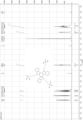
- FIG. 2 is a 1 HNMR chart of the compounds produced in Examples.
- FIG. 3 is a 1 HNMR chart of another compound produced in Examples.
- FIG. 4 is a 1 HNMR chart of still another compound produced in Examples.
- FIG. 5 is a 1 HNMR chart of still another compound produced in Examples.
- FIG. 6 is a 1 HNMR chart of still another compound produced in Examples.
- FIG. 7 is a 1 HNMR chart of still another compound produced in Examples.
- FIG. 8 is a 1 HNMR chart of still another compound produced in Examples.
- photoelectric conversion element of the present invention includes both “first photoelectric conversion element of the present invention” and “second photoelectric conversion element of the present invention” unless otherwise specified.
- the hole transport layer may contain a compound represented by the following chemical formula (I).
- Ar 1 is a structure containing an aromatic ring, and may or may not contain a heteroatom in the atoms constituting the aromatic ring, Ar 1 may or may not have a substituent other than -L 1 -X 1 , -L 1 -X 1 may be one or more, and when there are more than one, each L 1 and each X 1 may be the same or different, each L 1 is an atomic group or a covalent bond connecting Ar 1 and X 1 ; Each X1 is a group capable of transferring charge to and from the first electrode.
- the number of -L 1 -X 1 is not particularly limited, but may range from 1 to 4, for example.
- Ar 1 in chemical formula (I) may be represented by chemical formula (I-1) below.
- Ar 11 is an atomic group containing a cyclic structure, and the cyclic structure may be either an aromatic ring or a non-aromatic ring, and may be a monocyclic ring, a condensed ring, or a spiro ring.
- Ar 12 is an aromatic ring, which may or may not contain a heteroatom among the atoms constituting the ring;
- Ar 12 may be united with Ar 11 by sharing one or more atoms with Ar 11 ;
- Ar 12 may be one or more, and when there are more than one, they may be the same or different.
- the number of Ar 12 is not particularly limited, but may range from 1 to 4, for example.
- the Ar 11 may be represented by any one of the following chemical formulas (a1) to (a10).
- each Ar 12 in the chemical formula (I-1) may be represented by the following chemical formula (b).
- the carbon atoms C 1 and C 2 also serve as part of the atoms constituting the ring structure of Ar 11 in the chemical formula (I-1),
- the R 1 is a hydrogen atom, X 1 in the chemical formula (I), or a substituent, the substituent may or may not contain a hydrogen atom, and the hydrogen atom in the substituent at least one of may be substituted with X 1 in the chemical formula (I),
- Each R 11 may be the same or different, and each is a hydrogen atom or a substituent, or two adjacent R 11 are combined with the benzene ring to which they are bonded to form a condensed ring. may be
- Each R 11 may or may not have a further substituent.
- the chemical formula (b) may be represented by any one of the following chemical formulas (b1) to (b7).
- the compound represented by the chemical formula (I) may be a compound represented by any one of the following chemical formulas A-1 to A-23.
- Each R 1 is a hydrogen atom, X 1 in the chemical formula (I), or a substituent further substituted with X 1 in the chemical formula (I), and the same but can be different, at least one of the R 1 is X 1 in the chemical formula (I) or a substituent further substituted with X 1 in the chemical formula (I);
- the R 2 is a substituent, and may be one or more, or may not be present, and when there are multiple, each R 2 may be the same or different.
- R 1 when R 1 is a substituent further substituted with X 1 in the chemical formula (I), the number of X 1 may be 1 or plural. Further, when R 1 is a substituent further substituted by X 1 in the chemical formula (I), it is, for example, an alkyl group or an alkoxy group further substituted by X 1 in the chemical formula (I). may
- substituents R 2 are not particularly limited.
- the substituents R 2 may also be, for example, alkyl groups, alkoxy groups, or halo groups (halogen atoms), respectively.
- the compound represented by the chemical formula (I) has the following chemical formulas 4PATAT, 1-legged-3PATAT, 1-legged-3PATAT-H, 2-legged-3PATAT, 4PATTI-C3, Or it may be a compound represented by 4PATTI-C4.
- the hole transport layer may further contain a co-adsorbent.
- the co-adsorbent may be a compound represented by the following chemical formula (II).
- L 2 is an alkyl group, an alkoxy group, an aryl group, or a heterocyclic ring, at least one hydrogen atom of L 2 is substituted with X 2 , and it has a substituent other than X 2 may or may not have X 2 is a group capable of transferring charge to and from the first electrode, and may be one or more, and if there are more than one, they may be the same or different.
- the co-adsorbent may have a molecular weight of 2,000 or less.
- the photoelectric conversion layer may contain an organic-inorganic perovskite compound.
- the organic-inorganic perovskite compound may contain at least one of tin and lead.
- the photoelectric conversion element of the present invention may be, for example, a solar cell.
- the number of -L 1 -X 1 in the chemical formula (I) may be in the range of 1-4.
- Ar 1 may be represented by the following chemical formula (I-1).
- Ar 11 is an atomic group containing a cyclic structure, and the cyclic structure may be either an aromatic ring or a non-aromatic ring, and may be a monocyclic ring, a condensed ring, or a spiro ring.
- Ar 12 is an aromatic ring, which may or may not contain a heteroatom among the atoms constituting the ring;
- Ar 12 may be united with Ar 11 by sharing one or more atoms with Ar 11 ;
- Ar 12 may be one or more, and when there are more than one, they may be the same or different.
- the number of Ar 12 is not particularly limited, but may range from 1 to 4, for example.
- Ar 11 may be represented by any one of the following chemical formulas (a1) to (a10).
- each Ar 12 may be represented by the following chemical formula (b).
- the carbon atoms C 1 and C 2 also serve as part of the atoms constituting the ring structure of Ar 11 in the chemical formula (I-1),
- the R 1 is a hydrogen atom, X 1 in the chemical formula (I), or a substituent, the substituent may or may not contain a hydrogen atom, and the hydrogen atom in the substituent at least one of may be substituted with X 1 in the chemical formula (I),
- Each R 11 may be the same or different, and each is a hydrogen atom or a substituent, or two adjacent R 11 are combined with the benzene ring to which they are bonded to form a condensed ring. may be
- Each R 11 may or may not have a further substituent.
- the chemical formula (b) may be represented by any one of the following chemical formulas (b1) to (b7).
- the compound represented by the chemical formula (I) may be a compound represented by any one of the following chemical formulas A-1 to A-23.
- Each R 1 is a hydrogen atom, X 1 in the chemical formula (I), or a substituent further substituted with X 1 in the chemical formula (I), and the same but can be different, at least one of the R 1 is X 1 in the chemical formula (I) or a substituent further substituted with X 1 in the chemical formula (I);
- the R 2 is a substituent, and may be one or more, or may not be present, and when there are multiple, each R 2 may be the same or different.
- R 1 when R 1 is a substituent further substituted with X 1 in the chemical formula (I), the number of X 1 may be 1 or plural. Further, when R 1 is a substituent further substituted by X 1 in the chemical formula (I), it is, for example, an alkyl group or an alkoxy group further substituted by X 1 in the chemical formula (I). may
- substituents R 2 are not particularly limited.
- the substituents R 2 may also be, for example, alkyl groups, alkoxy groups, or halo groups (halogen atoms), respectively.
- the compound represented by the chemical formula (I) is a compound represented by the following chemical formula 4PATAT, 1-legged-3PATAT, 1-legged-3PATAT-H, 2-legged-3PATAT, 4PATTI-C3, or 4PATTI-C4 There may be.
- X 1 in the chemical formula (I) is at least one hydrogen of a group capable of transferring charge to and from an electrode instead of a group capable of transferring charge to and from an electrode. It may be a group in which atoms are substituted with further substituents.
- the substituents may be, for example, alkyl groups or halogen atoms, and if there are multiple substituents, they may be the same or different.
- each R in each X 1 is a substituent, and when there are a plurality of them, they may be the same or different.
- each of the substituents R in each X 1 in the chemical formula (I) may be, for example, an alkyl group or a halogen atom.
- the compound represented by the chemical formula (I) is the following chemical formula 4PAE-TAT, 1-legged-3PAE-TAT-H, 1-legged-3PAEE-TAT, 2-legged-3PAH-TAT, 4PATTI-C3, or 4PATTI It may be a compound represented by -C4.
- a chain group or atomic group e.g., a hydrocarbon group such as an alkyl group or an unsaturated aliphatic hydrocarbon group
- a hydrocarbon group such as an alkyl group or an unsaturated aliphatic hydrocarbon group
- a chain group or atomic group may be linear or branched, unless otherwise specified. is not particularly limited, but is, for example, 1 to 40, 1 to 32, 1 to 24, 1 to 18, 1 to 12, 1 to 6, or 1 to 2 (2 or more in the case of an unsaturated hydrocarbon group). It can be.
- the number of ring members (the number of atoms constituting the ring) of a cyclic group or atomic group is For example, without limitation, it may be 5-32, 5-24, 6-18, 6-12, or 6-10.
- any isomers may be used unless otherwise specified.
- simply referred to as a "naphthyl group” may be a 1-naphthyl group or a 2-naphthyl group.
- the "substituent” is not particularly limited, but examples include alkyl groups, unsaturated aliphatic hydrocarbon groups, alkoxy groups, aralkyl groups, aryl groups, heteroaryl groups, halogens, hydroxy groups (--OH), A mercapto group (-SH), an alkylthio group (-SR, R is an alkyl group), a sulfo group, a nitro group, a diazo group, a cyano group, a trifluoromethyl group and the like.
- any isomer Bodies can also be used in the present invention.
- the salt when a compound can form a salt, the salt can also be used in the present invention unless otherwise specified.
- the salt may be an acid addition salt or a base addition salt.
- the acid forming the acid addition salt may be an inorganic acid or an organic acid
- the base forming the base addition salt may be an inorganic base or an organic base.
- inorganic acid examples include, but are not limited to, sulfuric acid, phosphoric acid, hydrofluoric acid, hydrochloric acid, hydrobromic acid, hydroiodic acid, hypofluorous acid, hypochlorous acid, hypobromous acid, Hypoiodous acid, fluorous acid, chlorous acid, bromous acid, iodous acid, fluoric acid, chloric acid, bromic acid, iodic acid, perfluoric acid, perchloric acid, perbromic acid, periodic acid, etc. is given.
- the organic acid is also not particularly limited, but examples thereof include p-toluenesulfonic acid, methanesulfonic acid, oxalic acid, p-bromobenzenesulfonic acid, carbonic acid, succinic acid, citric acid, benzoic acid and acetic acid.
- the inorganic base include, but are not limited to, ammonium hydroxide, alkali metal hydroxide, alkaline earth metal hydroxide, carbonate and hydrogen carbonate. Examples include sodium hydroxide, potassium hydroxide, potassium carbonate, sodium carbonate, sodium hydrogen carbonate, potassium hydrogen carbonate, calcium hydroxide and calcium carbonate.
- the organic base is also not particularly limited, and examples thereof include ethanolamine, triethylamine and tris(hydroxymethyl)aminomethane.
- the method for producing these salts is not particularly limited, either, and they can be produced, for example, by adding an acid or base as described above to the above compounds as appropriate by a known method.
- the first photoelectric conversion element of the present invention is The first electrode, the hole transport layer, the photoelectric conversion layer, the electron transport layer, and the second electrode are laminated in the order,
- the photoelectric conversion layer includes a perovskite structure,
- the hole transport layer has an ionization potential in the range of -5.4 eV to -5.7 eV.
- the second photoelectric conversion element of the present invention is The first electrode, the hole transport layer, the photoelectric conversion layer, the electron transport layer, and the second electrode are laminated in the order,
- the photoelectric conversion layer includes a perovskite structure,
- the hole transport layer is characterized by containing a compound represented by the following chemical formula (I).
- Ar 1 , L 1 and X 1 in the following chemical formula (I) are as described above.
- the number of -L 1 -X 1 is not particularly limited, but may range from 1 to 4, for example.
- the first electrode, the hole transport layer, the photoelectric conversion layer, the electron transport layer, and the second electrode are laminated in the order described above.
- the photoelectric conversion element of the present invention may contain other components other than the first electrode, the hole transport layer, the photoelectric conversion layer, the electron transport layer, and the second electrode, It does not have to be included.
- the first electrode and the hole transport layer may be directly laminated without any other component between them, or may be laminated with other component between them. good too.
- the hole-transporting layer and the photoelectric conversion layer may be directly laminated without any other constituents between them, or may be laminated with other constituents between them. good too.
- the photoelectric conversion layer and the electron-transporting layer may be directly laminated without any other component between them, or may be laminated with another component between them. good.
- the electron-transporting layer and the second electrode may be directly laminated with no other constituents between them, or may be laminated with other constituents between them. good too.
- Each component in the photoelectric conversion device of the present invention has an ionization potential of the hole transport layer in the range of ⁇ 5.4 eV to ⁇ 5.7 eV (first photoelectric conversion device of the present invention), or
- the hole transport layer is not particularly limited except that it contains the compound represented by the chemical formula (I) (the second photoelectric conversion device of the present invention). It may be the same as or conforming to the recommended battery).
- the hole transport layer is not particularly limited except that the ionization potential is ⁇ 5.4 eV to ⁇ 5.7 eV. It may or may not contain a compound that
- the hole transport layer is not particularly limited except that it contains the compound represented by the chemical formula (I). It may be within the range of 0.7 eV or may be outside the range.
- the photoelectric conversion element of the present invention is not limited to the following examples.
- the case where the photoelectric conversion element of this invention is a solar cell is mainly demonstrated below.
- the photoelectric conversion element 10 includes a support (also referred to as a substrate, base material, etc.) 11, a first electrode 12, a hole transport layer 13, a photoelectric conversion layer 14, an electron transport layer 15, and a second Two electrodes 16 are stacked in the order described above.
- the support 11 is not particularly limited, and for example, a substrate that can be used for a general photoelectric conversion element such as a solar cell may be appropriately used.
- the substrate include glass, plastic plates, plastic films, inorganic crystals, and the like.
- Substrates having at least one film selected from a metal film, a semiconductor film, a conductive film and an insulating film formed on part or all of the surface of these substrates can also be suitably used as the support 11. can be done.
- the size, thickness, etc. of the support 11 are also not particularly limited, and may be, for example, similar to or conforming to general photoelectric conversion elements such as solar cells.
- the first electrode 12 is, for example, a layer that supports the hole transport layer 13 and has a function of extracting holes from the photoelectric conversion layer 14 .
- the first electrode 12 is, for example, a layer that functions as a cathode (positive electrode).
- the first electrode 12 may be formed directly on the support 11, for example.
- the first electrode 12 may be, for example, a transparent electrode made of a conductor.
- the transparent electrode is not particularly limited, examples thereof include tin-doped indium oxide (ITO) film, impurity-doped indium oxide (In 2 O 3 ) film, impurity-doped zinc oxide (ZnO) film, fluorine-doped tin dioxide ( FTO) film, a laminated film formed by laminating two or more of these, gold, silver, copper, aluminum, tungsten, titanium, chromium, nickel, cobalt, and the like. These may be used singly or as a mixture of two or more, and may be a single layer or a laminate.
- These films may also function, for example, as anti-diffusion layers.
- the thickness of the first electrode 12 is not particularly limited, it is preferably adjusted so that the sheet resistance is 5 to 15 ⁇ / ⁇ (per unit area), for example.
- the method for forming the first electrode 12 is not particularly limited, for example, it can be obtained by a known film forming method depending on the material to be formed.
- the shape of the first electrode 12 is not particularly limited.
- the method for forming the first electrode 12 on the support 11 is not particularly limited, for example, a known method may be used, and vacuum deposition such as vacuum deposition or sputtering is preferred. A patterned one may be used as the first electrode 12 .
- the patterning method is not limited to two, but includes, for example, a method of immersing in a laser or an etching solution, a method of patterning using a mask during vacuum film formation, etc. Any method may be used in the present invention.
- the first electrode 12 may be used together with a metal wiring or the like for the purpose of lowering the electrical resistance value.
- the material of the metal wiring is not particularly limited, but examples thereof include aluminum, copper, silver, gold, platinum and nickel.
- the metal lead wire can be used in combination by forming the metal lead wire on the first substrate by, for example, vapor deposition, sputtering, pressure bonding, etc., and providing a layer of ITO or FTO thereon, or providing it on ITO or FTO. be.
- the hole transport layer 13 has an ionization potential in the range of ⁇ 5.4 eV to ⁇ 5.7 eV (the first photoelectric conversion element of the present invention), or is represented by the chemical formula (I) (second photoelectric conversion element of the present invention).
- the hole transport layer 13 is not particularly limited, and may be, for example, similar to or conforming to the hole transport layer of a general photoelectric conversion element (for example, a general battery).
- the ionization potential of the hole-transport layer 13 is ⁇ 5.4 eV.
- the ionization potential of the hole transport layer 13 is ⁇ 5.7 eV or higher. Preferably.
- the compound represented by the chemical formula (I) can be used.
- the chemical formula (I) is, for example, as described above.
- L 1 in the chemical formula (I) include, in addition to the above, a divalent alkylene group such as a 1,1-methylene group and a 1,2-ethylene group, and a divalent group such as diethoxyethane. and the like, which may or may not have substituents other than X 1 .
- a phosphonic acid group, a trihalogenated silyl group, and a trialkoxysilyl group are preferable from the viewpoint of being able to bond firmly with the first electrode 12 (for example, a transparent electrode).
- the compound represented by the chemical formula (I) can be used, for example, as a hole transport compound that forms a monomolecular layer on the transparent conductive film.
- the transparent conductive film is, for example, the first electrode that is a transparent electrode, and the transparent electrode is, for example, ITO or the like as described above.
- the compound represented by the chemical formula (I) has an ionization potential of ⁇ 5.4 eV or less, so that it is difficult to react with oxygen and a device (element) can be stably produced. A highly durable photoelectric conversion element can be obtained.
- the method for forming the hole transport layer 13 is not particularly limited. can be formed.
- the method of adsorbing the compound represented by the chemical formula (I) to the first electrode 12 to form a monomolecular layer is not particularly limited, but for example, the compound represented by the chemical formula (I) is dissolved in a solvent and then contact and bond with the first electrode 12 .
- the bond between the compound represented by the chemical formula (I) and the first electrode 12 is not particularly limited, and may be a physical bond or a chemical bond.
- the type of the bond is also not particularly limited, and may be, for example, a hydrogen bond, an ester bond, a chelate bond, or the like.
- the solvent for dissolving the compound represented by the chemical formula (I) is also not particularly limited, and may be either or both of water and an organic solvent.
- the solvent include, more specifically, water, alcohols such as methanol, ethanol and 2-propanol, ethers such as diethyl ether and diisopropyl ether, ketones such as acetone and methyl isobutyl ketone, ethyl acetate, esters such as isobutyl acetate and ⁇ -butyrolactone; heterocycles such as tetrahydrofuran and thiophene; amides such as N,N-dimethylformamide, N,N-dimethylacetamide and N-methylpyrrolidone; sulfoxides such as dimethylsulfoxide; Sulfones such as diethylsulfone and sulfolane; Nitriles such as acetonitrile and 3-methoxypropionitrile; Aromatic compounds such as benz
- a specific method for forming a monomolecular layer by adsorbing the compound represented by the chemical formula (I) on the first electrode 12 is not particularly limited, but examples include dipping, spraying, spin coating, A known method such as a bar coat method can be used.
- the temperature during adsorption is not particularly limited, but is preferably -20°C to 100°C, more preferably 0°C to 50°C.
- the adsorption time is also not particularly limited, but is preferably 1 second to 48 hours, more preferably 10 seconds to 1 hour.
- washing may or may not be performed.
- the washing method is also not particularly limited, and for example, a known method may be used as appropriate.
- Heat treatment may or may not be performed after the adsorption treatment or after the washing.
- the temperature of the heat treatment is preferably 50°C to 150°C, more preferably 70°C to 120°C.
- the heat treatment time is preferably 1 second to 48 hours, more preferably 10 seconds to 1 hour. Moreover, this heat treatment may be performed in the air or in a vacuum, for example.
- a co-adsorbent When the compound represented by the chemical formula (I) is adsorbed on the first electrode 12, for example, a co-adsorbent may be used together, or may not be used together.
- the co-adsorbent is added for the purpose of, for example, when the compound represented by the chemical formula (I) alone cannot completely cover the electrode surface, or for the purpose of inhibiting the interaction between the compounds represented by the chemical formula (I). can do.
- the coadsorbent is not particularly limited, for example, as described above, the compound represented by the chemical formula (II) can be used.
- the L 2 and X 2 in the chemical formula (II) are, for example, as described above.
- Specific examples of the compound represented by the chemical formula (II) are not particularly limited, but for example, n-butylphosphonic acid, n-hexylphosphonic acid, n-decylphosphonic acid, n-octadecylphosphonic acid, 2-ethylhexyl Phosphonic acid compounds such as phosphonic acid, methoxymethylphosphonic acid, 3-acryloyloxypropylphosphonic acid, 11-hydroxyundecylphosphonic acid, 1H,1H,2H,2H-perfluorophosphonic acid, acetic acid, propionic acid, isobutyric acid, nonane acid, fluoroacetic acid, ⁇ -chloropropionic acid, glyoxylic acid, etc., and these may be used alone or in combination of two or more.
- the molecular weight of the compound represented by the chemical formula (II) is not particularly limited. may be The smaller the molecular weight, the higher the coverage when forming a layer on the electrode (for example, ITO), so the smaller the molecular weight, the better.
- the method of adsorbing the co-adsorbent to the first electrode 12 is not particularly limited, but a method of dissolving it in a solvent and then adsorbing it is preferable, as in the case of the compound represented by the chemical formula (I).
- the solvent is also not particularly limited, but may be, for example, the same solvents as those exemplified above for the compound represented by the chemical formula (I).
- the co-adsorbent may be adsorbed by immersing the first electrode 12 in a solvent in which the co-adsorbent is dissolved after the compound represented by the chemical formula (I) is once adsorbed on the substrate. , and the compound represented by the above chemical formula (I) may be mixed and dissolved in an organic solvent.
- the photoelectric conversion layer 14 is not particularly limited, and may be, for example, the same photoelectric conversion layer used in a general photoelectric conversion element such as a solar cell.
- the photoelectric conversion layer 14 contains, for example, a perovskite compound.
- the perovskite compound may be, for example, a compound represented by the following chemical formula (III). X ⁇ Y ⁇ Z ⁇ . . . (III)
- the ratio of ⁇ : ⁇ : ⁇ is 3:1:1, and ⁇ and ⁇ represent integers greater than 1.
- X represents a halogen ion
- Y represents an amino group-containing organic compound
- Z represents a metal ion.
- the perovskite layer is preferably positioned adjacent to the electron transport layer. Note that the ratio of ⁇ : ⁇ : ⁇ does not necessarily have to be 3:1:1, such as 3:1.05:0.95.
- X in the chemical formula (III) is not particularly limited and can be appropriately selected depending on the purpose.
- examples thereof include halogen ions such as chlorine, bromine, and iodine. These may be used individually by 1 type, and may use 2 or more types together.
- Y in the chemical formula (III) includes alkylamine compound ions (organic compounds having an amino group) such as methylamine, ethylamine, n-butylamine, and formamidine, and alkalis such as cesium, potassium, and rubidium, which are not limited to organic compounds.
- Metal ions are mentioned.
- the alkylamine compound ions and alkali metal ions may be used singly or in combination of two or more.
- Organic (alkylamine compound ions) and inorganic (alkali metal ions) can also be used in combination. For example, cesium ions and formamidine may be used in combination.
- Z in the chemical formula (III) is not particularly limited and can be appropriately selected according to the purpose.
- examples include metals such as lead, indium, antimony, tin, copper, and bismuth. These may be used individually by 1 type, and may use 2 or more types together. Especially lead Among them, combination of lead and tin is particularly preferable.
- the perovskite layer preferably exhibits a layered perovskite structure in which a layer composed of a metal halide and a layer in which organic cation molecules are arranged are alternately laminated.
- the perovskite layer may contain alkali metals. If the perovskite layer contains at least an alkali metal, it is advantageous in terms of high output.
- Alkali metals include, for example, cesium, rubidium, and potassium. Among these, cesium is preferred.
- the photoelectric conversion layer 14 may be a perovskite layer formed from a perovskite compound, as described above.
- the method for forming such a perovskite layer is not particularly limited and can be appropriately selected according to the purpose. A drying method and the like can be mentioned.
- a solution in which a metal halide is dissolved or dispersed is applied, dried, and then immersed in a solution in which an alkylamine halide is dissolved to form a perovskite compound.
- a stepwise precipitation method and the like can be mentioned.
- a poor solvent a solvent with low solubility
- a method of precipitating and the like can be mentioned.
- a perovskite layer includes, for example, a method of vapor-depositing a metal halide in a gas filled with methylamine or the like.
- a method for forming the perovskite layer a method of precipitating crystals by adding a poor solvent for the perovskite compound while applying a solution in which the metal halide and the alkylamine halide are dissolved or dispersed is particularly preferable.
- the method of applying these solutions is not particularly limited and can be appropriately selected depending on the purpose. be done.
- a method of applying the solution for example, a method of precipitating in a supercritical fluid using carbon dioxide or the like may be used.
- the poor solvent used includes hydrocarbons such as n-hexane and n-octane, alcohols such as methanol, ethanol and 2-propanol, diethyl ether, Ethers such as diisopropyl ether, ketones such as acetone and methyl isobutyl ketone, esters such as ethyl acetate, isobutyl acetate and ⁇ -butyrolactone, nitriles such as acetonitrile and 3-methoxypropionitrile, benzene, toluene, chlorobenzene, etc. aromatic hydrocarbon compounds, halogen-based solvents such as dichloromethane and chloroform, and fluorine-based solvents such as chlorofluorocarbons, hydrochlorofluorocarbons and hydrofluorocarbons.
- hydrocarbons such as n-hexane and n-octane
- alcohols such as methanol, ethanol and 2-prop
- the thickness of the photoelectric transport layer 14 is not particularly limited, but from the viewpoint of further suppressing performance deterioration due to defects and peeling, it is preferably 50 to 1200 nm, more preferably 200 to 600 nm. .
- the material used for the electron transport layer 15 is not particularly limited and can be appropriately selected depending on the purpose, but a semiconductor material is preferable.
- the semiconductor material is not particularly limited, and known materials can be used. Examples thereof include single semiconductors, compound semiconductors, organic n-type semiconductors, and the like.
- the single semiconductor is not particularly limited, but examples thereof include silicon and germanium.
- the compound semiconductor is not particularly limited, but for example, metal chalcogenides, specifically titanium, tin, zinc, iron, tungsten, zirconium, hafnium, strontium, indium, cerium, yttrium, lanthanum, vanadium, niobium, oxides such as tantalum; sulfides such as cadmium, zinc, lead, silver, antimony and bismuth; selenides such as cadmium and lead; tellurides such as cadmium; Other compound semiconductors include phosphides such as zinc, gallium, indium and cadmium, gallium arsenide, copper-indium-selenide and copper-indium-sulfide.
- organic n-type semiconductor examples include, but are not limited to, perylenetetracarboxylic anhydride, perylenetetracarboxydiimide compound, naphthalenediimide-bithiophene copolymer, benzobisimidazobenzophenanthroline polymer, C60, C70, PCBM ( [6,6]-phenyl-C 61 -butyric acid methyl ester), carbonyl bridge-bithiazole compounds, ALq3 (tris(8-quinolinolato)aluminum), triphenylene bipyridyl compounds, silole compounds, oxadiazole compounds, etc. can be mentioned.
- an organic n-type semiconductor is particularly preferable.
- the materials used for forming the electron transport layer 15 may be used singly or in combination of two or more.
- the crystal type of the semiconductor material is not particularly limited and can be appropriately selected according to the purpose, and may be single crystal, polycrystal, or amorphous.
- the thickness of the electron-transporting layer 15 is not particularly limited and can be appropriately selected according to the purpose.
- the method for forming the electron transport layer 15 is not particularly limited, and can be appropriately selected according to the purpose. Examples thereof include a method of forming a thin film in vacuum (vacuum film forming method), a wet film forming method, and the like.
- Vacuum film forming methods include, for example, a sputtering method, a pulse laser deposition method (PLD method), an ion beam sputtering method, an ion assist method, an ion plating method, a vacuum vapor deposition method, an atomic layer deposition method (ALD method), Chemical vapor deposition method (CVD method) etc. are mentioned.
- the wet film-forming method examples include a method of applying a solvent in which an electron-transporting material is dissolved, and a sol-gel method in the case of an oxide semiconductor.
- the sol-gel method is a method in which a gel is produced from a solution through chemical reactions such as hydrolysis and polymerization/condensation, and then densification is promoted by heat treatment.
- the method of applying the sol solution is not particularly limited and can be appropriately selected depending on the purpose.
- method, blade coating method, gravure coating method, and wet printing methods include letterpress, offset, gravure, intaglio, rubber plate, screen printing and the like.
- the temperature for the heat treatment after applying the sol solution is preferably 80° C. or higher, more preferably 100° C. or higher.
- An electron injection layer may be formed between the electron transport layer 15 and the second electrode 16 after forming the electron transport layer 15 .
- BCP bathoproine
- the thickness of the electron injection layer is preferably 1 nm to 100 nm, more preferably 3 nm to 20 nm.
- the second electrode 16 (which may be, for example, a back electrode) is a layer having a function of extracting electrons from the photoelectric conversion layer 14 via an electron transport layer, for example. Also, the second electrode 16 is a layer that functions as an anode (negative electrode), for example.
- the second electrode 16 may be formed directly on the electron transport layer (also called electron injection layer) 15 .
- the material of the second electrode 16 is not particularly limited, and for example, the same material as that of the first electrode 12 can be used.
- the shape, structure, and size of the second electrode 16 are not particularly limited, and can be appropriately selected according to the purpose.
- Materials for the second electrode 16 include metals, carbon compounds, conductive metal oxides, and conductive polymers.
- Examples of the metal include platinum, gold, silver, copper, and aluminum.
- Examples of the carbon compound include graphite, fullerene, carbon nanotube, and graphene.
- Examples of the conductive metal oxide include ITO, FTO, and ATO.
- Examples of the conductive polymer include polythiophene and polyaniline.
- the materials used for forming the second electrode 16 may be used singly or in combination of two or more.
- the second electrode 16 can be appropriately formed on the electron transport layer 15 by using a method such as coating, lamination, vacuum deposition, CVD, or bonding depending on the type of material used and the type of the hole transport layer 13. be.
- At least one of the first electrode 12 and the second electrode 16 is preferably substantially transparent.
- the electrodes transparent and allow incident light to enter from the electrode side.
- a material that reflects light for the back electrode such as metal, glass deposited with a conductive oxide, or plastic.
- a metal thin film, and the like are preferably used. It is also effective to provide an antireflection layer on the electrode on the incident light side.
- the configuration of the photoelectric conversion element of the present invention is not limited to the configuration of FIG.
- the support 11 is arranged on the side opposite to that in FIG. Layer 14, hole transport layer 13, and first electrode 12 may be stacked in the order described above.
- other constituent elements are provided between the layers of the support 11, the first electrode 12, the hole transport layer 13, the photoelectric conversion layer 14, the electron transport layer 15, and the second electrode 16. It may or may not exist.
- the photoelectric conversion element of the present invention is not limited to this.
- the first electrode may be the back electrode and the second electrode may be the transparent electrode.
- the photoelectric conversion element of the present invention (for example, a solar cell) is preferably sealed to protect the device (photoelectric conversion element of the present invention) from water and oxygen.
- the structure of the sealing is not particularly limited, it may be, for example, the same as that of a general photoelectric conversion element (for example, a solar cell). It may be coated and covered with glass or film, or the entire surface of the photoelectric conversion element of the present invention may be coated with the sealing material and covered with glass or film, or the entire surface of the photoelectric conversion element of the present invention may be covered with the sealing material. It may be applied only.
- the material of the sealing member is not particularly limited, and can be appropriately selected according to the purpose.
- epoxy resin or acrylic resin is preferably used and cured. It does not matter if only the coating is cured.
- the epoxy resin is not particularly limited, but includes, for example, water dispersion type, solventless type, solid type, heat curing type, curing agent mixed type, ultraviolet curing type, etc. Among them, thermosetting type and ultraviolet curing type is preferred, and an ultraviolet curable type is more preferred. It should be noted that even if it is an ultraviolet curing type, it is possible to heat, and it is preferable to heat even after ultraviolet curing.
- Specific examples of epoxy resins include bisphenol A type, bisphenol F type, novolac type, cycloaliphatic type, long chain aliphatic type, glycidylamine type, glycidyl ether type, glycidyl ester type, etc., and these can be used alone.
- Epoxy resin compositions that are already commercially available can be used in the present invention. Among others, there are epoxy resin compositions developed and marketed for use in solar cells and organic EL devices, which can be used particularly effectively in the present invention.
- epoxy resin compositions include, for example, TB3118, TB3114, TB3124, TB3125F (manufactured by ThreeBond Co., Ltd.), WorldRock5910, WorldRock5920, WorldRock8723 (manufactured by Kyoritsu Chemical Sangyo Co., Ltd.), WB90US(P), and WB90US-HV. (manufactured by Moresco) and the like.
- acrylic resin is not particularly limited, for example, those developed and commercially available for use in solar cells and organic EL elements can be effectively used.
- Commercially available acrylic resin compositions include, for example, TB3035B and TB3035C (manufactured by ThreeBond Co., Ltd.).
- the curing agent is not particularly limited and can be appropriately selected depending on the intended purpose. Examples thereof include amine-based, acid anhydride-based, polyamide-based and other curing agents.
- Amine-based curing agents include aliphatic polyamines such as diethylenetriamine and triethylenetetramine; aromatic polyamines such as metaphenylenediamine, diaminodiphenylmethane and diaminodiphenylsulfone; and acid anhydride-based curing agents include phthalic anhydride.
- curing agents include imidazoles and polymercaptans. These may be used alone or in combination of two or more.
- the additive is not particularly limited and can be appropriately selected depending on the intended purpose. agents, plasticizers, coloring agents, flame retardant aids, antioxidants, organic solvents, and the like. Among these, fillers, gap agents, curing accelerators, polymerization initiators, and desiccants (hygroscopic agents) are preferred, and fillers and polymerization initiators are more preferred.
- a filler as an additive, it suppresses the infiltration of moisture and oxygen, further reduces volume shrinkage during curing, reduces outgassing during curing or heating, improves mechanical strength, and thermal conductivity. and the control of fluidity can be obtained. Therefore, including a filler as an additive is very effective in maintaining stable output in various environments.
- the filler is not particularly limited and can be appropriately selected depending on the purpose. Examples include crystalline or amorphous silica, silicate minerals such as talc, alumina, aluminum nitride, silicon nitride, and calcium silicate. and inorganic fillers such as calcium carbonate. Among these, hydrotalcite is particularly preferred. Moreover, these may be used alone or in combination of two or more.
- the average primary particle size of the filler is not particularly limited, it is preferably 0.1 ⁇ m or more and 10 ⁇ m or less, more preferably 1 ⁇ m or more and 5 ⁇ m or less.
- the average primary particle size of the filler is within the above preferable range, the effect of suppressing penetration of moisture and oxygen can be sufficiently obtained, the viscosity becomes appropriate, the adhesion to the substrate and the defoaming property are improved. It is also effective for controlling the width of the sealing portion and workability.
- the content of the filler is preferably 10 parts by mass or more and 90 parts by mass or less, more preferably 20 parts by mass or more and 70 parts by mass or less, relative to the entire sealing member (100 parts by mass).
- the content of the filler is within the above preferable range, the effect of suppressing penetration of moisture and oxygen is sufficiently obtained, the viscosity becomes appropriate, and the adhesion and workability become good.
- the gap agent is also called a gap control agent or a spacer agent.
- the gap material By including the gap material as an additive, it becomes possible to control the gap of the seal. For example, when a sealing member is provided on the first substrate or the first electrode, and the second substrate is placed thereon for sealing, the sealing member must be mixed with a gap agent. As a result, the gap of the sealing portion is aligned with the size of the gap agent, so that the gap of the sealing portion can be easily controlled.
- the gap agent is not particularly limited, for example, one that is granular, has a uniform particle size, and has high solvent resistance and heat resistance is preferable, and can be appropriately selected according to the purpose.
- the gap agent preferably has a high affinity with epoxy resin and has a spherical particle shape. Specifically, glass beads, silica fine particles, organic resin fine particles and the like are preferable. These may be used individually by 1 type, and may use 2 or more types together.
- the particle diameter of the gap agent can be selected according to the gap of the sealing portion to be set, but is preferably 1 ⁇ m or more and 100 ⁇ m or less, more preferably 5 ⁇ m or more and 50 ⁇ m or less.
- the polymerization initiator is not particularly limited, but includes, for example, a polymerization initiator that initiates polymerization using heat or light, and can be appropriately selected depending on the purpose.
- a polymerization initiator and the like are included.
- Thermal polymerization initiators are compounds that generate active species such as radicals and cations by heating, and include azo compounds such as 2,2'-azobisbutyronitrile (AIBN) and benzoyl peroxide (BPO). Examples include peroxides.
- a benzenesulfonic acid ester, an alkylsulfonium salt, or the like is used as the thermal cationic polymerization initiator.
- a photocationic polymerization initiator is preferably used in the case of an epoxy resin.
- a cationic photopolymerization initiator is mixed with an epoxy resin and irradiated with light, the cationic photopolymerization initiator decomposes to generate an acid, which causes polymerization of the epoxy resin and a curing reaction proceeds.
- a photocationic polymerization initiator has effects such as little volume shrinkage during curing, no oxygen inhibition, and high storage stability.
- photocationic polymerization initiator examples include aromatic diazonium salts, aromatic iodonium salts, aromatic sulfonium salts, metacelone compounds, and silanol/aluminum complexes.
- a photoacid generator having a function of generating an acid upon irradiation with light can also be used as the polymerization initiator.
- the photoacid generator acts as an acid that initiates cationic polymerization, and includes ionic sulfonium salt-based and iodonium salt-based onium salts composed of a cation portion and an anion portion. These may be used alone or in combination of two or more.
- the amount of the polymerization initiator added is not particularly limited and may vary depending on the material used, but is preferably 0.5 parts by mass or more and 10 parts by mass or less with respect to the entire sealing member (100 parts by mass). 1 part by mass or more and 5 parts by mass or less is more preferable.
- the desiccant (also referred to as a hygroscopic agent) is a material that has the function of physically or chemically adsorbing and absorbing moisture. can be reduced.
- the desiccant is not particularly limited and can be appropriately selected depending on the purpose, but is preferably particulate, such as calcium oxide, barium oxide, magnesium oxide, magnesium sulfate, sodium sulfate, calcium chloride. , silica gel, molecular sieves, and zeolites. Among these, zeolites with high moisture absorption are preferred. These may be used alone or in combination of two or more.
- the curing accelerator (also called a curing catalyst) is a material that accelerates the curing speed, and is mainly used for thermosetting epoxy resins.
- the curing accelerator is not particularly limited and can be appropriately selected depending on the intended purpose.
- -tertiary amines or tertiary amine salts such as diazabicyclo(4,3,0)-nonene-5
- imidazoles such as 1-cyanoethyl-2-ethyl-4-methylimidazole and 2-ethyl-4-methylimidazole
- phosphines such as triphenylphosphine and tetraphenylphosphonium/tetraphenylborate
- phosphonium salts may be used alone or in combination of two or more.
- the coupling agent is not particularly limited as long as it is a material that has the effect of increasing molecular bonding strength, and can be appropriately selected according to the purpose.
- Examples include silane coupling agents. Specifically, 3-glycidoxypropyltrimethoxysilane, 3-glycidoxypropylmethyldimethoxysilane, 3-glycidoxypropylmethyldimethoxysilane, 2-(3,4-epoxycyclohexyl)ethyltrimethoxysilane, N-phenyl- ⁇ -aminopropyltrimethoxysilane, N-(2-aminoethyl)3-aminopropylmethyldimethoxysilane, N-(2-aminoethyl)3-aminopropylmethyltrimethoxysilane, 3-aminopropyltrimethoxysilane Silane cups such as ethoxysilane, 3-mercaptopropyltrimethoxysilane, vinyltrime
- a sheet adhesive can be used.
- the sheet adhesive is, for example, a sheet on which a resin layer is formed in advance, and the sheet can be made of glass, a film having a high gas barrier property, or the like. Also, the sheet may be formed only from the sealing resin. It is also possible to apply a sheet adhesive onto the sealing film. It is also possible to form a structure in which a hollow portion is provided on the sealing film and then attach it to the device.
- the photoelectric conversion device is arranged so as to face the support.
- the shape, structure, size and type of the sealing film base material are not particularly limited and can be appropriately selected according to the purpose.
- the sealing film forms a barrier layer that prevents passage of moisture and oxygen on the surface of the base material, and may be formed on only one side or both sides of the base material.
- the barrier layer may be composed of a material containing, for example, a metal oxide, a metal, a mixture formed of a polymer and a metal alkoxide, or the like as a main component.
- the metal oxide include aluminum oxide, silicon oxide, aluminum, and the like.
- the polymer include polyvinyl alcohol, polyvinylpyrrolidone, methylcellulose, and the like. Examples include tetraethoxysilane, triisopropoxyaluminum, 3-glycidoxypropyltrimethoxysilane, 3-mercaptopropyltrimethoxysilane, 3-isocyanatopropyltriethoxysilane and the like.
- the barrier layer may be transparent or opaque, for example. Moreover, the barrier layer may be a single layer made of a combination of the above materials, or may be a multi-layered structure.
- a method for forming the barrier layer known methods can be used, and coating methods such as vacuum film formation such as sputtering, dipping, roll coating, screen printing, spraying, and gravure printing can be used. can.
- the photoelectric conversion element for example, a solar cell
- Lead wires are connected to the first electrode and the second electrode using a conductive material such as solder, silver paste, or graphite, for example.
- the conductive material may be used singly or in a mixed or laminated structure of two or more.
- the part where the lead wire is attached may be covered with an acrylic resin or an epoxy resin.
- a lead wire is a general term for electric wires for electrically connecting power supplies and electronic components in an electric circuit, and examples include vinyl wires and enameled wires.
- the application and method of use of the photoelectric conversion device of the present invention are not particularly limited, and for example, it can be widely used in the same applications as general photoelectric conversion devices (for example, general solar cells).
- the photoelectric conversion element (for example, a solar cell) of the present invention can be applied to a power supply device, for example, by combining it with a circuit board or the like that controls the generated current.
- Devices that use power supply devices include, for example, electronic desk calculators and solar radio-controlled wristwatches.
- auxiliary power supply for extending the continuous use time of rechargeable or dry battery electric appliances, or a secondary battery. It can also be used as an independent power supply that does not require battery replacement or power supply wiring.
- the yield (%) is the yield (mol%) based on the amount of substance (mol) unless otherwise specified.
- NMR (nuclear magnetic resonance) spectra were measured using AV400M manufactured by Bruker.
- Example A1 Synthesis of 4-PATAT
- 4-PATAT which is one of the compounds of the present invention (compounds represented by the above chemical formula (I))
- Example A2 Synthesis of 1-legged-3PATAT]
- 1-legged-3PATAT which is one of the compounds of the present invention (compounds represented by the above chemical formula (I))
- 1-legged-3PAE-TAT (215 mg), ethyl iodide (0.141 mg), and DMF (4.1 mL) were placed in a three-necked flask, and sodium hydride (43.4 mg) was added under an argon gas stream at room temperature while stirring. was added slowly. Stirring was continued for 1.5 hours, water was added to stop the reaction, and the mixture was extracted with ethyl acetate. After drying with sodium sulfate, the solvent was distilled off. The residue was purified by silica gel column chromatography (eluent: toluene) to obtain 147 mg of brown oily 1-legged-3PAEE-TAT (see the chemical formula in Scheme 5 above). The yield was 63% based on the starting 1-legged-3PAE-TAT.
- 1-legged-3PAEE-TAT 115 mg
- dichloromethane 5.4 mL
- trimethylsilane bromide 0.10 mg
- methanol 3.6 mL
- Example A3 Synthesis of 1-legged-3PATAT-H]
- 1-legged-3PATAT-H which is one of the compounds of the present invention (the compound represented by the chemical formula (I))
- 2-legged-3PAH-TAT 47 mg
- dichloromethane 2.8 mL
- trimethylsilane bromide 0.124 mg
- TTI 23.0 mg, 50 mmol
- cesium carbonate 130 mg, 400 mmol
- tetrabutylammonium bromide 6.4 mg, 20 mmol
- tetrahydrofuran 1 ml
- diethyl(3-bromopropyl)phosphonate 58 mL
- 300 mmol was added, and the mixture was heated and stirred at 80° C. for 1 hour. After cooling to room temperature, the organic layer extracted with dichloromethane was dried over magnesium sulfate.
- the yellow oily mixture obtained by concentration under reduced pressure was purified by silica gel chromatography (eluent ethyl acetate:methanol 1:1 ⁇ 1:2) to give 47.5 mg (41 mmol, yield 81) of the target compound 1. %, yellow oil).
- TTI 23.0 g, 50 mmol
- cesium carbonate 130 mg, 400 mmol
- tetrabutylammonium bromide 6.4 mg, 20 mmol
- 1,4-dibromobutane 36 mL, 300 mmol
- water was added to stop the reaction, and the mixture was extracted with dichloromethane three times. The separated organic layer was dried over magnesium sulfate, and the solvent was distilled off under reduced pressure.
- Example 1 A solar cell, which is a photoelectric conversion element of the present invention, was produced (manufactured) in the following manner.
- C60 with a thickness of 20 nm (electron transport layer), bathocuproine (BCP, 8 nm) (electron injection layer), and Ag (100 nm) (second electrode) were formed by vacuum deposition to produce a photoelectric conversion device.
- BCP, 8 nm bathocuproine
- Ag 100 nm
- the photoelectric conversion characteristics of the sealed device produced in Example 1 were measured by a method conforming to JISC8913:1998 for measuring the output of silicon crystal solar cells.
- a solar simulator (SMO-250III model manufactured by Spectroscopy Instruments Co., Ltd.) combined with an air mass filter equivalent to AM 1.5G was used as a light source for measurement by adjusting the light intensity to 100 mW/cm 2 with a secondary reference Si solar cell, and using a perovskite solar cell.
- the IV curve characteristics were measured using a source meter (manufactured by Keithley Instruments Inc., model 2400 general-purpose source meter).
- the short-circuit current (Isc), open-circuit voltage (Voc), fill factor (FF), short-circuit current density (Jsc), and photoelectric conversion efficiency (PCE) obtained from the V-curve characteristic measurement are expressed in the following equations 1 and 2. was calculated using The results are shown in Table 1 below. Also, this device was placed in a dryer at 85° C. in a dark place, and the photoelectric conversion efficiency was measured for 500 hours. The results are also shown in Table 1.
- Example 2 Example 1 except that the DMF solution of 4PATAT (0.1 mmol/L) in Example 1 was changed to a DMF solution of 4PATAT (0.1 mmol/L) and n-butylphosphonic acid (0.1 mmol/L). A photoelectric conversion element was produced (manufactured) in the same manner, and the photoelectric conversion efficiency was measured. The results are shown in Table 1 below. The IP (ionization potential) measured in the same manner as in Example 1 was -5.41 eV.
- Example 3 A photoelectric conversion element was produced in the same manner as in Example 1 except that the DMF solution of 4PATAT (0.1 mmol/L) in Example 1 was changed to a DMF solution of 1-legged-3PATAT (0.1 mmol/L) ( manufacturing), and the photoelectric conversion efficiency was measured. The results are shown in Table 1 below. The IP measured in the same manner as in Example 1 was -5.64 eV.
- Example 4 A photoelectric conversion element was produced in the same manner as in Example 1, except that the DMF solution of 4PATAT (0.1 mmol/L) in Example 1 was changed to a DMF solution of 1-legged-3PATAT-H (0.1 mmol/L). It was produced (manufactured) and the photoelectric conversion efficiency was measured. The results are shown in Table 1 below. The IP measured in the same manner as in Example 1 was -5.68 eV.
- Example 5 A photoelectric conversion element was produced in the same manner as in Example 1 except that the DMF solution of 4PATAT (0.1 mmol/L) in Example 1 was changed to the DMF solution of 2-legged-3PATAT (0.1 mmol/L) ( manufacturing), and the photoelectric conversion efficiency was measured. The results are shown in Table 1 below. The IP measured in the same manner as in Example 1 was -5.54 eV.
- Example 6 Except for changing the DMF solution of 4PATAT (0.1 mmol/L) in Example 1 to a DMF solution of 2-legged-3PATAT (0.1 mmol/L) and n-butylphosphonic acid (0.1 mmol/L) A photoelectric conversion element was produced (manufactured) in the same manner as in Example 1, and the photoelectric conversion efficiency was measured. The results are shown in Table 1 below. The IP measured in the same manner as in Example 1 was -5.50 eV.
- Example 7 Except for changing the DMF solution of 4PATAT (0.1 mmol/L) in Example 1 to a DMF solution of 1-legged-3PATAT (0.1 mmol/L) and n-butylphosphonic acid (0.1 mmol/L) A photoelectric conversion element was produced (manufactured) in the same manner as in Example 1, and the photoelectric conversion efficiency was measured. The results are shown in Table 1 below. The IP measured in the same manner as in Example 1 was -5.45 eV.
- Example 8 Example except that the DMF solution of 4PATAT (0.1 mmol/L) in Example 1 was changed to a DMF solution of 4PATTI-C3 (0.1 mmol/L) and n-butylphosphonic acid (0.1 mmol/L) A photoelectric conversion element was produced (manufactured) in the same manner as in 1, and the photoelectric conversion efficiency was measured. The results are shown in Table 2 below. Further, the IP (ionization potential) measured in the same manner as in Example 1 was ⁇ 5.57 eV.
- Example 9 Example except that the DMF solution of 4PATAT (0.1 mmol/L) in Example 1 was changed to a DMF solution of 4PATAT-C4 (0.1 mmol/L) and n-butylphosphonic acid (0.1 mmol/L) A photoelectric conversion element was produced (manufactured) in the same manner as in 1, and the photoelectric conversion efficiency was measured. The results are shown in Table 2 below.
- the IP (ionization potential) measured in the same manner as in Example 1 was -5.52 eV.
- Example 1 A photoelectric conversion element was produced in the same manner as in Example 1 except that the DMF solution of 4PATAT (0.1 mmol/L) in Example 1 was changed to a DMF solution of n-butylphosphonic acid (0.1 mmol/L) ( manufacturing), and the photoelectric conversion efficiency was measured. The results are shown in Table 1 below. The IP measured in the same manner as in Example 1 was -5.48 eV.
- Example 2 Example except that the DMF solution of 4PATAT (0.1 mmol/L) in Example 1 was changed to a DMF solution of [2-(9H-carbazol-9-yl)ethyl]phosphonic acid (0.1 mmol/L) A photoelectric conversion element was produced (manufactured) in the same manner as in 1, and the photoelectric conversion efficiency was measured. The results are shown in Table 1 below. Moreover, the ionization potential when this compound was adsorbed on the ITO substrate was -5.91 eV.
- Example 3 A DMF solution of 4PATAT (0.1 mmol/L) in Example 1 was added to a DMF solution of [2-(3,6-Dimethoxy-9H-carbazol-9-yl)ethyl]phosphonic Acid (0.1 mmol/L).
- a photoelectric conversion element was produced (manufactured) in the same manner as in Example 1, except for the change, and the photoelectric conversion efficiency was measured. The results are shown in Table 1 below. Also, the ionization potential when this compound was adsorbed on the ITO substrate was -5.25 eV.
- the photoelectric conversion device of the present invention is useful, for example, as a solar cell.
- the application and method of use of the photoelectric conversion device of the present invention are not particularly limited. be.
- the compound of the present invention for the hole transport layer of the photoelectric conversion device of the present invention for example, a photoelectric conversion device exhibiting excellent photoelectric conversion characteristics and having high durability can be obtained.
- the application and method of use of the compound of the present invention are not limited to this, and can be applied to any wide range of fields.
Abstract
A purpose of the present invention is to provide a photoelectric conversion element having a hole transport layer that exhibits excellent photoelectric conversion characteristics, and having a high durability. In order to achieve this purpose, the photoelectric conversion element according to the present invention has a first electrode (12), a hole transport layer (13), a photoelectric conversion layer (14), an electron transport layer (15), and a second electrode (16) stacked in that order, and is characterized in that the photoelectric conversion layer (14) includes a perovskite structure, and that the hole transport layer (13) has an ionization potential in the range of -5.4 eV to -5.7 eV.
Description
本発明は、光電変換素子及び化合物に関する。
The present invention relates to photoelectric conversion elements and compounds.
近年、クリーンエネルギーとして、太陽光発電が注目を浴びており、太陽電池の開発が進んでいる。その一つとして、低コストで製造可能な次世代型の太陽電池として、ペロブスカイト材料を光吸収層に用いた太陽電池が急速に注目を集めている。例えば、非特許文献1では、ペロブスカイト材料を光吸収層に用いた溶液型の太陽電池が報告されている。また、非特許文献2には、固体型のペロブスカイト型太陽電池が高効率を示すことも報告されている。
In recent years, photovoltaic power generation has attracted attention as clean energy, and the development of solar cells is progressing. As one of them, a solar cell using a perovskite material for a light absorption layer is rapidly attracting attention as a next-generation solar cell that can be manufactured at low cost. For example, Non-Patent Document 1 reports a solution-type solar cell using a perovskite material for a light absorption layer. Non-Patent Document 2 also reports that a solid-state perovskite solar cell exhibits high efficiency.
ペロブスカイト型太陽電池の基本構造としては、電極の上に、電子輸送層、光吸収層(ペロブスカイト層)、正孔輸送層(ホール輸送層とも言う)及び裏面電極をこの順に積層する順型構造、電極の上に、正孔輸送層、光吸収層、電子輸送層及び裏面電極を個の順に積層する逆型構造が知られている。電子輸送層とペロブスカイト層との間に多孔質形状からなる電子輸送層を備えることもある。このうち、正孔輸送層には、一般的には、有機半導体の正孔輸送性材料が用いられている(例えば、非特許文献3~10)。
The basic structure of a perovskite solar cell is a normal structure in which an electron-transporting layer, a light-absorbing layer (perovskite layer), a hole-transporting layer (also called a hole-transporting layer), and a backside electrode are stacked in this order on an electrode. An inverted structure is known in which a hole-transporting layer, a light-absorbing layer, an electron-transporting layer and a backside electrode are laminated in order on an electrode. A porous electron transport layer may be provided between the electron transport layer and the perovskite layer. Of these layers, the hole-transporting layer generally uses an organic semiconductor hole-transporting material (eg, Non-Patent Documents 3 to 10).
しかしながら、従来のペロブスカイト型太陽電池は、その光電変換効率が十分とは言えない。太陽電池の光電変換効率を改善するためには、特に、正孔輸送層の特性の改善が重要である。正孔輸送層に用いる正孔輸送性材料としては、例えば、これまでに、トラクセン化合物(非特許文献3)、ジケトピロロピロール化合物(非特許文献4)、チオフェン化合物(非特許文献5、6)、ジチエノピロール(非特許文献7)等が報告されている。しかし、ペロブスカイト型太陽電池として有用と言えるほどの光電変換効率を発揮することができる化合物はほとんど報告されていない。そこで、色素増感型太陽電池用の正孔輸送材料として開発されたSpiro-OMeTAD([2,2',7,7'-テトラキス(N,N-ジ-p-メトキシフェニルアミノ)-9,9'-スピロビフルオレン])が提案されているが、耐熱性が低いことが知られている(非特許文献8)。また、PTAA(ポリ[ビス(4-フェニル)(2,4,6-トリメチルフェニル)アミン])とよばれるトリフェニルアミン骨格をもつポリマー材料も耐光性が低いことが知られている。さらに、これらの材料をpバッファ層用の正孔輸送材料として用いる場合、添加物としてLiTFSI塩(リチウムビス(トリフルオロメタンスルホニル)イミド)を加えて導電性を改良する必要があり、これが素子の劣化の原因の一つになってしまうと考えられる(非特許文献9)。また、近年、ホスホン酸を有するカルバゾール型の正孔輸送材料が報告された(非特許文献10)。この化合物は透明電極として用いられているインジウムスズ化合物(ITO)と反応し、透明電極上で単分子層を形成するものである。この化合物は、20%を超える光電変換効率が報告されており、非常に有効な化合物であるが、一方で、V1036という化合物をITOに吸着した状態でのイオン化ポテンシャル(IP)が-4.98eVであり、容易に酸化されやすい(すなわち耐久性が低い)。このような現状から、特に正孔輸送層が優れた光電変換特性を示し、かつ高い耐久性を有する材料が求められている。
However, conventional perovskite solar cells cannot be said to have sufficient photoelectric conversion efficiency. In order to improve the photoelectric conversion efficiency of solar cells, it is particularly important to improve the properties of the hole transport layer. Examples of hole-transporting materials used in the hole-transporting layer include traxene compounds (Non-Patent Document 3), diketopyrrolopyrrole compounds (Non-Patent Document 4), thiophene compounds (Non-Patent Documents 5 and 6 ), dithienopyrrole (Non-Patent Document 7), etc. have been reported. However, almost no compounds have been reported that can exhibit a photoelectric conversion efficiency that can be said to be useful as a perovskite solar cell. Therefore, Spiro-OMeTAD ([2,2',7,7'-tetrakis(N,N-di-p-methoxyphenylamino)-9, which was developed as a hole transport material for dye-sensitized solar cells, 9′-spirobifluorene]) has been proposed, but it is known to have low heat resistance (Non-Patent Document 8). A polymer material having a triphenylamine skeleton called PTAA (poly[bis(4-phenyl)(2,4,6-trimethylphenyl)amine]) is also known to have low light resistance. Furthermore, when these materials are used as hole-transporting materials for the p-buffer layer, it is necessary to add LiTFSI salt (lithium bis(trifluoromethanesulfonyl)imide) as an additive to improve conductivity, which leads to deterioration of the device. (Non-Patent Document 9). In recent years, a carbazole-type hole-transporting material containing phosphonic acid has also been reported (Non-Patent Document 10). This compound reacts with an indium tin compound (ITO) used as a transparent electrode to form a monomolecular layer on the transparent electrode. This compound has been reported to have a photoelectric conversion efficiency exceeding 20%, and is a very effective compound. and is easily oxidized (that is, has low durability). Under such circumstances, there is a demand for a material in which the hole transport layer in particular exhibits excellent photoelectric conversion characteristics and high durability.
そこで、本発明は、正孔輸送層が優れた光電変換特性を示し、かつ高い耐久性を有する光電変換素子、及び化合物の提供を目的とする。
Therefore, an object of the present invention is to provide a photoelectric conversion element and a compound in which a hole transport layer exhibits excellent photoelectric conversion characteristics and has high durability.
前記目的を達成するために、本発明の第1の光電変換素子は、
第1の電極、正孔輸送層、光電変換層、電子輸送層、及び第2の電極が、前記順序で積層され、
前記光電変換層は、ペロブスカイト構造を含み、
前記正孔輸送層は、イオン化ポテンシャルが-5.4eV~-5.7eVの範囲であることを特徴とする。 In order to achieve the above object, the first photoelectric conversion device of the present invention is
The first electrode, the hole transport layer, the photoelectric conversion layer, the electron transport layer, and the second electrode are laminated in the order,
The photoelectric conversion layer includes a perovskite structure,
The hole transport layer has an ionization potential in the range of -5.4 eV to -5.7 eV.
本発明の第2の光電変換素子は、
第1の電極、正孔輸送層、光電変換層、電子輸送層、及び第2の電極が、前記順序で積層され、
前記光電変換層は、ペロブスカイト構造を含み、
前記正孔輸送層は、下記化学式(I)で表される化合物を含むことを特徴とする。

前記化学式(I)において、
Ar1は、芳香環を含む構造であり、前記芳香環を構成する原子中にヘテロ原子を含んでいても含んでいなくてもよく、
Ar1は、-L1-X1以外の置換基を有していても有していなくてもよく、
-L1-X1は、1つでも複数でもよく、複数の場合は、各L1及び各X1は、互いに同一であっても異なっていてもよく、
各L1は、Ar1とX1とを結合する原子団であるか、又は共有結合であり、
各X1は、それぞれ、前記第1の電極との間で電荷を授受可能な基である。 The second photoelectric conversion element of the present invention is
The first electrode, the hole transport layer, the photoelectric conversion layer, the electron transport layer, and the second electrode are laminated in the order,
The photoelectric conversion layer includes a perovskite structure,
The hole transport layer is characterized by containing a compound represented by the following chemical formula (I).
In the chemical formula (I),
Ar 1 is a structure containing an aromatic ring, and may or may not contain a heteroatom in the atoms constituting the aromatic ring,
Ar 1 may or may not have a substituent other than -L 1 -X 1 ,
-L 1 -X 1 may be one or more, and when there are more than one, each L 1 and each X 1 may be the same or different,
each L 1 is an atomic group or a covalent bond connecting Ar 1 and X 1 ;
Each X1 is a group capable of transferring charge to and from the first electrode.
第1の電極、正孔輸送層、光電変換層、電子輸送層、及び第2の電極が、前記順序で積層され、
前記光電変換層は、ペロブスカイト構造を含み、
前記正孔輸送層は、下記化学式(I)で表される化合物を含むことを特徴とする。
Ar1は、芳香環を含む構造であり、前記芳香環を構成する原子中にヘテロ原子を含んでいても含んでいなくてもよく、
Ar1は、-L1-X1以外の置換基を有していても有していなくてもよく、
-L1-X1は、1つでも複数でもよく、複数の場合は、各L1及び各X1は、互いに同一であっても異なっていてもよく、
各L1は、Ar1とX1とを結合する原子団であるか、又は共有結合であり、
各X1は、それぞれ、前記第1の電極との間で電荷を授受可能な基である。 The second photoelectric conversion element of the present invention is
The first electrode, the hole transport layer, the photoelectric conversion layer, the electron transport layer, and the second electrode are laminated in the order,
The photoelectric conversion layer includes a perovskite structure,
The hole transport layer is characterized by containing a compound represented by the following chemical formula (I).
Ar 1 is a structure containing an aromatic ring, and may or may not contain a heteroatom in the atoms constituting the aromatic ring,
Ar 1 may or may not have a substituent other than -L 1 -X 1 ,
-L 1 -X 1 may be one or more, and when there are more than one, each L 1 and each X 1 may be the same or different,
each L 1 is an atomic group or a covalent bond connecting Ar 1 and X 1 ;
Each X1 is a group capable of transferring charge to and from the first electrode.
本発明の化合物は、下記化学式(I)で表されることを特徴とする。

前記化学式(I)において、
Ar1は、芳香環を含む構造であり、前記芳香環を構成する原子中にヘテロ原子を含んでいても含んでいなくてもよく、
Ar1は、-L1-X1以外の置換基を有していても有していなくてもよく、
-L1-X1は、1つでも複数でもよく、複数の場合は、各L1及び各X1は、互いに同一であっても異なっていてもよく、
各L1は、Ar1とX1とを結合する原子団であるか、又は共有結合であり、
各X1は、それぞれ、電極との間で電荷を授受可能な基である。 The compound of the present invention is characterized by being represented by the following chemical formula (I).
In the chemical formula (I),
Ar 1 is a structure containing an aromatic ring, and may or may not contain a heteroatom in the atoms constituting the aromatic ring,
Ar 1 may or may not have a substituent other than -L 1 -X 1 ,
-L 1 -X 1 may be one or more, and when there are more than one, each L 1 and each X 1 may be the same or different,
each L 1 is an atomic group or a covalent bond connecting Ar 1 and X 1 ;
Each X1 is a group capable of transferring charge to and from an electrode.
Ar1は、芳香環を含む構造であり、前記芳香環を構成する原子中にヘテロ原子を含んでいても含んでいなくてもよく、
Ar1は、-L1-X1以外の置換基を有していても有していなくてもよく、
-L1-X1は、1つでも複数でもよく、複数の場合は、各L1及び各X1は、互いに同一であっても異なっていてもよく、
各L1は、Ar1とX1とを結合する原子団であるか、又は共有結合であり、
各X1は、それぞれ、電極との間で電荷を授受可能な基である。 The compound of the present invention is characterized by being represented by the following chemical formula (I).
Ar 1 is a structure containing an aromatic ring, and may or may not contain a heteroatom in the atoms constituting the aromatic ring,
Ar 1 may or may not have a substituent other than -L 1 -X 1 ,
-L 1 -X 1 may be one or more, and when there are more than one, each L 1 and each X 1 may be the same or different,
each L 1 is an atomic group or a covalent bond connecting Ar 1 and X 1 ;
Each X1 is a group capable of transferring charge to and from an electrode.
本発明によれば、正孔輸送層が優れた光電変換特性を示し、かつ高い耐久性を有する光電変換素子、及び化合物を提供することができる。
According to the present invention, it is possible to provide a photoelectric conversion element and a compound in which a hole transport layer exhibits excellent photoelectric conversion characteristics and has high durability.
つぎに、本発明について、例を挙げてさらに詳細に説明する。ただし、本発明は、以下の説明により限定されない。
Next, the present invention will be described in more detail with examples. However, the invention is not limited by the following description.
以下において「本発明の光電変換素子」という場合は、特に断らない限り、「本発明の第1の光電変換素子」及び「本発明の第2の光電変換素子」の両方を含む。
Hereinafter, the term "photoelectric conversion element of the present invention" includes both "first photoelectric conversion element of the present invention" and "second photoelectric conversion element of the present invention" unless otherwise specified.
本発明の第1の光電変換素子は、例えば、前記正孔輸送層が、下記化学式(I)で表される化合物を含んでいてもよい。
In the first photoelectric conversion element of the present invention, for example, the hole transport layer may contain a compound represented by the following chemical formula (I).

前記化学式(I)において、
Ar1は、芳香環を含む構造であり、前記芳香環を構成する原子中にヘテロ原子を含んでいても含んでいなくてもよく、
Ar1は、-L1-X1以外の置換基を有していても有していなくてもよく、
-L1-X1は、1つでも複数でもよく、複数の場合は、各L1及び各X1は、互いに同一であっても異なっていてもよく、
各L1は、Ar1とX1とを結合する原子団であるか、又は共有結合であり、
各X1は、それぞれ、前記第1の電極との間で電荷を授受可能な基である。
-L1-X1の数は、特に限定されないが、例えば、1~4の範囲でもよい。 In the chemical formula (I),
Ar 1 is a structure containing an aromatic ring, and may or may not contain a heteroatom in the atoms constituting the aromatic ring,
Ar 1 may or may not have a substituent other than -L 1 -X 1 ,
-L 1 -X 1 may be one or more, and when there are more than one, each L 1 and each X 1 may be the same or different,
each L 1 is an atomic group or a covalent bond connecting Ar 1 and X 1 ;
Each X1 is a group capable of transferring charge to and from the first electrode.
The number of -L 1 -X 1 is not particularly limited, but may range from 1 to 4, for example.
本発明の光電変換素子は、例えば、
前記化学式(I)において、
各X1が、それぞれ、ホスホン酸基(-P=O(OH)2)、カルボキシ基(-COOH)、スルホ基(-SO3H)、ボロン酸基(-B(OH)2)、トリハロゲン化シリル基(-SiX3、ただしXはハロ基)、又はトリアルコキシシリル基(-Si(OR)3、ただしRはアルキル基)であってもよい。 The photoelectric conversion device of the present invention is, for example,
In the chemical formula (I),
Each X 1 is, respectively, a phosphonic acid group (-P=O(OH) 2 ), a carboxy group (-COOH), a sulfo group (-SO 3 H), a boronic acid group (-B(OH) 2 ), a tri It may be a silyl halide group (-SiX 3 where X is a halo group) or a trialkoxysilyl group (-Si(OR) 3 where R is an alkyl group).
本発明の光電変換素子は、例えば、前記化学式(I)において、前記Ar1が、下記化学式(I-1)で表されてもよい。
In the photoelectric conversion device of the present invention, for example, Ar 1 in chemical formula (I) may be represented by chemical formula (I-1) below.

前記化学式(I-1)中、
Ar11は、環状構造を含む原子団であり、前記環状構造は、芳香環でも非芳香環でもよく、単環でも縮合環でもスピロ環でもよく、環を構成する原子中にヘテロ原子を含んでいても含んでいなくてもよく、
Ar12は、芳香環であり、環を構成する原子中にヘテロ原子を含んでいても含んでいなくてもよく、
Ar12は、1つ以上の原子をAr11と共有してAr11と一体化していてもよく、
Ar12は、1つでも複数でもよく、複数の場合は互いに同一でも異なっていてもよい。
Ar12の数は特に限定されないが、例えば、1~4の範囲でもよい。 In the chemical formula (I-1),
Ar 11 is an atomic group containing a cyclic structure, and the cyclic structure may be either an aromatic ring or a non-aromatic ring, and may be a monocyclic ring, a condensed ring, or a spiro ring. which may or may not contain
Ar 12 is an aromatic ring, which may or may not contain a heteroatom among the atoms constituting the ring;
Ar 12 may be united with Ar 11 by sharing one or more atoms with Ar 11 ;
Ar 12 may be one or more, and when there are more than one, they may be the same or different.
The number of Ar 12 is not particularly limited, but may range from 1 to 4, for example.
本発明の光電変換素子は、例えば、前記化学式(I-1)において、前記Ar11が、下記化学式(a1)~(a10)のいずれかで表されてもよい。
In the photoelectric conversion device of the present invention, for example, in the chemical formula (I-1), the Ar 11 may be represented by any one of the following chemical formulas (a1) to (a10).

本発明の光電変換素子は、例えば、前記化学式(I-1)において、前記各Ar12が、それぞれ下記化学式(b)で表されてもよい。
In the photoelectric conversion device of the present invention, for example, each Ar 12 in the chemical formula (I-1) may be represented by the following chemical formula (b).

前記化学式(b)において、
炭素原子C1及びC2は、前記化学式(I-1)中の前記Ar11における前記環状構造を構成する原子の一部を兼ねており、
前記R1は、水素原子、前記化学式(I)中のX1、又は置換基であり、前記置換基は水素原子を含んでいても含んでいなくてもよく、前記置換基中の水素原子の少なくとも一つは、前記化学式(I)中のX1で置換されていてもよく、
前記各R11は、互いに同一でも異なっていてもよく、それぞれ水素原子若しくは置換基であるか、又は、隣接する2つのR11は、それらが結合するベンゼン環と一体となって縮合環を形成していてもよく、
前記各R11は、さらに置換基を有していても有していなくてもよい。 In the chemical formula (b),
The carbon atoms C 1 and C 2 also serve as part of the atoms constituting the ring structure of Ar 11 in the chemical formula (I-1),
The R 1 is a hydrogen atom, X 1 in the chemical formula (I), or a substituent, the substituent may or may not contain a hydrogen atom, and the hydrogen atom in the substituent at least one of may be substituted with X 1 in the chemical formula (I),
Each R 11 may be the same or different, and each is a hydrogen atom or a substituent, or two adjacent R 11 are combined with the benzene ring to which they are bonded to form a condensed ring. may be
Each R 11 may or may not have a further substituent.
本発明の光電変換素子は、例えば、前記化学式(b)が、下記化学式(b1)~(b7)のいずれかで表されてもよい。
In the photoelectric conversion device of the present invention, for example, the chemical formula (b) may be represented by any one of the following chemical formulas (b1) to (b7).

本発明の光電変換素子は、例えば、前記化学式(I)で表される化合物が、下記化学式A-1~A-23のいずれかで表される化合物であってもよい。
In the photoelectric conversion device of the present invention, for example, the compound represented by the chemical formula (I) may be a compound represented by any one of the following chemical formulas A-1 to A-23.


前記化学式A-1~A-23において、
前記各R1は、それぞれ、水素原子であるか、前記化学式(I)中のX1であるか、又は、前記化学式(I)中のX1でさらに置換された置換基であり、互いに同一でも異なっていてもよく、
前記各R1のうち少なくとも1つは、前記化学式(I)中のX1であるか、又は、前記化学式(I)中のX1でさらに置換された置換基であり、
前記R2は、置換基であり、1つでも複数でも存在しなくてもよく、複数の場合は、各R2は、互いに同一でも異なっていてもよい。 In the chemical formulas A-1 to A-23,
Each R 1 is a hydrogen atom, X 1 in the chemical formula (I), or a substituent further substituted with X 1 in the chemical formula (I), and the same but can be different,
at least one of the R 1 is X 1 in the chemical formula (I) or a substituent further substituted with X 1 in the chemical formula (I);
The R 2 is a substituent, and may be one or more, or may not be present, and when there are multiple, each R 2 may be the same or different.
前記化学式A-1~A-23において、R1が、前記化学式(I)中のX1でさらに置換された置換基である場合は、X1の数は、1でも複数でもよい。また、R1が、前記化学式(I)中のX1でさらに置換された置換基である場合は、例えば、前記化学式(I)中のX1でさらに置換されたアルキル基又はアルコキシ基であってもよい。
In the chemical formulas A-1 to A-23, when R 1 is a substituent further substituted with X 1 in the chemical formula (I), the number of X 1 may be 1 or plural. Further, when R 1 is a substituent further substituted by X 1 in the chemical formula (I), it is, for example, an alkyl group or an alkoxy group further substituted by X 1 in the chemical formula (I). may
前記化学式A-1~A-23において、前記置換基R2の数は特に限定されない。また、前記置換基R2は、例えば、それぞれ、アルキル基、アルコキシ基、又はハロ基(ハロゲン原子)であってもよい。
In the chemical formulas A-1 to A-23, the number of substituents R 2 is not particularly limited. The substituents R 2 may also be, for example, alkyl groups, alkoxy groups, or halo groups (halogen atoms), respectively.
本発明の光電変換素子は、例えば、前記化学式(I)で表される化合物が、下記化学式4PATAT、1-legged-3PATAT、1-legged-3PATAT-H、2-legged-3PATAT、4PATTI-C3、又は4PATTI-C4で表される化合物であってもよい。
In the photoelectric conversion device of the present invention, for example, the compound represented by the chemical formula (I) has the following chemical formulas 4PATAT, 1-legged-3PATAT, 1-legged-3PATAT-H, 2-legged-3PATAT, 4PATTI-C3, Or it may be a compound represented by 4PATTI-C4.


本発明の光電変換素子は、例えば、前記正孔輸送層が、さらに、共吸着剤を含んでいてもよい。
In the photoelectric conversion device of the present invention, for example, the hole transport layer may further contain a co-adsorbent.
本発明の光電変換素子は、例えば、前記共吸着剤が、下記化学式(II)で表される化合物であってもよい。
In the photoelectric conversion device of the present invention, for example, the co-adsorbent may be a compound represented by the following chemical formula (II).

前記化学式(II)において、
L2は、アルキル基、アルコキシ基、又はアリール基、又はヘテロ環であり、L2の水素原子の少なくとも1つ以上がX2で置換されており、X2以外の置換基を有していても有してなくてもよく、
X2は、前記第1の電極との間で電荷を授受可能な基であり、1つでも複数でもよく、複数の場合は同一でも異なっていてもよい。 In the chemical formula (II),
L 2 is an alkyl group, an alkoxy group, an aryl group, or a heterocyclic ring, at least one hydrogen atom of L 2 is substituted with X 2 , and it has a substituent other than X 2 may or may not have
X 2 is a group capable of transferring charge to and from the first electrode, and may be one or more, and if there are more than one, they may be the same or different.
本発明の光電変換素子は、例えば、
前記化学式(II)において、
各X2が、それぞれ、ホスホン酸基(-P=O(OH)2)、カルボキシ基(-COOH)、スルホ基(-SO3H)、ボロン酸基(-B(OH)2)、トリハロゲン化シリル基(-SiX3、ただしXはハロ基)、又はトリアルコキシシリル基(-Si(OR)3、ただしRはアルキル基)であってもよい。 The photoelectric conversion device of the present invention is, for example,
In the chemical formula (II),
Each X 2 is, respectively, a phosphonic acid group (-P=O(OH) 2 ), a carboxy group (-COOH), a sulfo group (-SO 3 H), a boronic acid group (-B(OH) 2 ), a tri It may be a silyl halide group (-SiX 3 where X is a halo group) or a trialkoxysilyl group (-Si(OR) 3 where R is an alkyl group).
本発明の光電変換素子は、例えば、前記共吸着剤の分子量が2,000以下であってもよい。
In the photoelectric conversion device of the present invention, for example, the co-adsorbent may have a molecular weight of 2,000 or less.
本発明の光電変換素子は、例えば、前記光電変換層が、有機無機ペロブスカイト化合物を含んでいてもよい。
In the photoelectric conversion element of the present invention, for example, the photoelectric conversion layer may contain an organic-inorganic perovskite compound.
本発明の光電変換素子は、例えば、前記有機無機ペロブスカイト化合物が、スズ及び鉛の少なくとも一方を含んでいてもよい。
In the photoelectric conversion device of the present invention, for example, the organic-inorganic perovskite compound may contain at least one of tin and lead.
本発明の光電変換素子は、例えば、太陽電池であってもよい。
The photoelectric conversion element of the present invention may be, for example, a solar cell.
本発明の化合物は、例えば、前記化学式(I)において、-L1-X1の数が、1~4の範囲でもよい。
In the compound of the present invention, for example, the number of -L 1 -X 1 in the chemical formula (I) may be in the range of 1-4.
本発明の化合物は、例えば、
前記化学式(I)において、
各X1が、それぞれ、ホスホン酸基(-P=O(OH)2)、カルボキシ基(-COOH)、スルホ基(-SO3H)、ボロン酸基(-B(OH)2)、トリハロゲン化シリル基(-SiX3、ただしXはハロ基)、又はトリアルコキシシリル基(-Si(OR)3、ただしRはアルキル基)であってもよい。 Compounds of the invention are, for example,
In the chemical formula (I),
Each X 1 is, respectively, a phosphonic acid group (-P=O(OH) 2 ), a carboxy group (-COOH), a sulfo group (-SO 3 H), a boronic acid group (-B(OH) 2 ), a tri It may be a silyl halide group (-SiX 3 where X is a halo group) or a trialkoxysilyl group (-Si(OR) 3 where R is an alkyl group).
本発明の化合物は、例えば、
前記化学式(I)において、前記Ar1が、下記化学式(I-1)で表されてもよい。 Compounds of the invention are, for example,
In the chemical formula (I), Ar 1 may be represented by the following chemical formula (I-1).
前記化学式(I)において、前記Ar1が、下記化学式(I-1)で表されてもよい。 Compounds of the invention are, for example,
In the chemical formula (I), Ar 1 may be represented by the following chemical formula (I-1).

前記化学式(I-1)中、
Ar11は、環状構造を含む原子団であり、前記環状構造は、芳香環でも非芳香環でもよく、単環でも縮合環でもスピロ環でもよく、環を構成する原子中にヘテロ原子を含んでいても含んでいなくてもよく、
Ar12は、芳香環であり、環を構成する原子中にヘテロ原子を含んでいても含んでいなくてもよく、
Ar12は、1つ以上の原子をAr11と共有してAr11と一体化していてもよく、
Ar12は、1つでも複数でもよく、複数の場合は互いに同一でも異なっていてもよい。
Ar12の数は、特に限定されないが、例えば、1~4の範囲でもよい。 In the chemical formula (I-1),
Ar 11 is an atomic group containing a cyclic structure, and the cyclic structure may be either an aromatic ring or a non-aromatic ring, and may be a monocyclic ring, a condensed ring, or a spiro ring. which may or may not contain
Ar 12 is an aromatic ring, which may or may not contain a heteroatom among the atoms constituting the ring;
Ar 12 may be united with Ar 11 by sharing one or more atoms with Ar 11 ;
Ar 12 may be one or more, and when there are more than one, they may be the same or different.
The number of Ar 12 is not particularly limited, but may range from 1 to 4, for example.
本発明の化合物は、例えば、
前記化学式(I-1)において、前記Ar11が、下記化学式(a1)~(a10)のいずれかで表されてもよい。 Compounds of the invention are, for example,
In the chemical formula (I-1), Ar 11 may be represented by any one of the following chemical formulas (a1) to (a10).
前記化学式(I-1)において、前記Ar11が、下記化学式(a1)~(a10)のいずれかで表されてもよい。 Compounds of the invention are, for example,
In the chemical formula (I-1), Ar 11 may be represented by any one of the following chemical formulas (a1) to (a10).

本発明の化合物は、例えば、
前記化学式(I-1)において、前記各Ar12が、それぞれ下記化学式(b)で表されてもよい。 Compounds of the invention are, for example,
In the chemical formula (I-1), each Ar 12 may be represented by the following chemical formula (b).
前記化学式(I-1)において、前記各Ar12が、それぞれ下記化学式(b)で表されてもよい。 Compounds of the invention are, for example,
In the chemical formula (I-1), each Ar 12 may be represented by the following chemical formula (b).

前記化学式(b)において、
炭素原子C1及びC2は、前記化学式(I-1)中の前記Ar11における前記環状構造を構成する原子の一部を兼ねており、
前記R1は、水素原子、前記化学式(I)中のX1、又は置換基であり、前記置換基は水素原子を含んでいても含んでいなくてもよく、前記置換基中の水素原子の少なくとも一つは、前記化学式(I)中のX1で置換されていてもよく、
前記各R11は、互いに同一でも異なっていてもよく、それぞれ水素原子若しくは置換基であるか、又は、隣接する2つのR11は、それらが結合するベンゼン環と一体となって縮合環を形成していてもよく、
前記各R11は、さらに置換基を有していても有していなくてもよい。 In the chemical formula (b),
The carbon atoms C 1 and C 2 also serve as part of the atoms constituting the ring structure of Ar 11 in the chemical formula (I-1),
The R 1 is a hydrogen atom, X 1 in the chemical formula (I), or a substituent, the substituent may or may not contain a hydrogen atom, and the hydrogen atom in the substituent at least one of may be substituted with X 1 in the chemical formula (I),
Each R 11 may be the same or different, and each is a hydrogen atom or a substituent, or two adjacent R 11 are combined with the benzene ring to which they are bonded to form a condensed ring. may be
Each R 11 may or may not have a further substituent.
炭素原子C1及びC2は、前記化学式(I-1)中の前記Ar11における前記環状構造を構成する原子の一部を兼ねており、
前記R1は、水素原子、前記化学式(I)中のX1、又は置換基であり、前記置換基は水素原子を含んでいても含んでいなくてもよく、前記置換基中の水素原子の少なくとも一つは、前記化学式(I)中のX1で置換されていてもよく、
前記各R11は、互いに同一でも異なっていてもよく、それぞれ水素原子若しくは置換基であるか、又は、隣接する2つのR11は、それらが結合するベンゼン環と一体となって縮合環を形成していてもよく、
前記各R11は、さらに置換基を有していても有していなくてもよい。 In the chemical formula (b),
The carbon atoms C 1 and C 2 also serve as part of the atoms constituting the ring structure of Ar 11 in the chemical formula (I-1),
The R 1 is a hydrogen atom, X 1 in the chemical formula (I), or a substituent, the substituent may or may not contain a hydrogen atom, and the hydrogen atom in the substituent at least one of may be substituted with X 1 in the chemical formula (I),
Each R 11 may be the same or different, and each is a hydrogen atom or a substituent, or two adjacent R 11 are combined with the benzene ring to which they are bonded to form a condensed ring. may be
Each R 11 may or may not have a further substituent.
本発明の化合物は、例えば、
前記化学式(b)が、下記化学式(b1)~(b7)のいずれかで表されてもよい。 Compounds of the invention are, for example,
The chemical formula (b) may be represented by any one of the following chemical formulas (b1) to (b7).
前記化学式(b)が、下記化学式(b1)~(b7)のいずれかで表されてもよい。 Compounds of the invention are, for example,
The chemical formula (b) may be represented by any one of the following chemical formulas (b1) to (b7).

本発明の化合物は、例えば、
前記化学式(I)で表される化合物が、下記化学式A-1~A-23のいずれかで表される化合物であってもよい。 Compounds of the invention are, for example,
The compound represented by the chemical formula (I) may be a compound represented by any one of the following chemical formulas A-1 to A-23.
前記化学式(I)で表される化合物が、下記化学式A-1~A-23のいずれかで表される化合物であってもよい。 Compounds of the invention are, for example,
The compound represented by the chemical formula (I) may be a compound represented by any one of the following chemical formulas A-1 to A-23.


前記化学式A-1~A-23において、
前記各R1は、それぞれ、水素原子であるか、前記化学式(I)中のX1であるか、又は、前記化学式(I)中のX1でさらに置換された置換基であり、互いに同一でも異なっていてもよく、
前記各R1のうち少なくとも1つは、前記化学式(I)中のX1であるか、又は、前記化学式(I)中のX1でさらに置換された置換基であり、
前記R2は、置換基であり、1つでも複数でも存在しなくてもよく、複数の場合は、各R2は、互いに同一でも異なっていてもよい。 In the chemical formulas A-1 to A-23,
Each R 1 is a hydrogen atom, X 1 in the chemical formula (I), or a substituent further substituted with X 1 in the chemical formula (I), and the same but can be different,
at least one of the R 1 is X 1 in the chemical formula (I) or a substituent further substituted with X 1 in the chemical formula (I);
The R 2 is a substituent, and may be one or more, or may not be present, and when there are multiple, each R 2 may be the same or different.
前記各R1は、それぞれ、水素原子であるか、前記化学式(I)中のX1であるか、又は、前記化学式(I)中のX1でさらに置換された置換基であり、互いに同一でも異なっていてもよく、
前記各R1のうち少なくとも1つは、前記化学式(I)中のX1であるか、又は、前記化学式(I)中のX1でさらに置換された置換基であり、
前記R2は、置換基であり、1つでも複数でも存在しなくてもよく、複数の場合は、各R2は、互いに同一でも異なっていてもよい。 In the chemical formulas A-1 to A-23,
Each R 1 is a hydrogen atom, X 1 in the chemical formula (I), or a substituent further substituted with X 1 in the chemical formula (I), and the same but can be different,
at least one of the R 1 is X 1 in the chemical formula (I) or a substituent further substituted with X 1 in the chemical formula (I);
The R 2 is a substituent, and may be one or more, or may not be present, and when there are multiple, each R 2 may be the same or different.
前記化学式A-1~A-23において、R1が、前記化学式(I)中のX1でさらに置換された置換基である場合は、X1の数は、1でも複数でもよい。また、R1が、前記化学式(I)中のX1でさらに置換された置換基である場合は、例えば、前記化学式(I)中のX1でさらに置換されたアルキル基又はアルコキシ基であってもよい。
In the chemical formulas A-1 to A-23, when R 1 is a substituent further substituted with X 1 in the chemical formula (I), the number of X 1 may be 1 or plural. Further, when R 1 is a substituent further substituted by X 1 in the chemical formula (I), it is, for example, an alkyl group or an alkoxy group further substituted by X 1 in the chemical formula (I). may
前記化学式A-1~A-23において、前記置換基R2の数は特に限定されない。また、前記置換基R2は、例えば、それぞれ、アルキル基、アルコキシ基、又はハロ基(ハロゲン原子)であってもよい。
In the chemical formulas A-1 to A-23, the number of substituents R 2 is not particularly limited. The substituents R 2 may also be, for example, alkyl groups, alkoxy groups, or halo groups (halogen atoms), respectively.
本発明の化合物は、例えば、
前記化学式(I)で表される化合物が、下記化学式4PATAT、1-legged-3PATAT、1-legged-3PATAT-H、2-legged-3PATAT、4PATTI-C3、又は4PATTI-C4で表される化合物であってもよい。 Compounds of the invention are, for example,
The compound represented by the chemical formula (I) is a compound represented by the following chemical formula 4PATAT, 1-legged-3PATAT, 1-legged-3PATAT-H, 2-legged-3PATAT, 4PATTI-C3, or 4PATTI-C4 There may be.


本発明の化合物は、例えば、前記化学式(I)中のX1が、電極との間で電荷を授受可能な基に代えて、電極との間で電荷を授受可能な基の少なくとも一つの水素原子をさらなる置換基で置換した基であってもよい。前記置換基は、例えば、アルキル基、又はハロゲン原子であってもよく、複数の場合は互いに同一でも異なっていてもよい。
In the compound of the present invention, for example, X 1 in the chemical formula (I) is at least one hydrogen of a group capable of transferring charge to and from an electrode instead of a group capable of transferring charge to and from an electrode. It may be a group in which atoms are substituted with further substituents. The substituents may be, for example, alkyl groups or halogen atoms, and if there are multiple substituents, they may be the same or different.
本発明の化合物は、例えば、
前記化学式(I)において、
各X1が、それぞれ、ホスホン酸エステル基(-P=O(OR)2)、カルボン酸エステル基(-COOR)、スルホン酸エステル基(-SO3R)、又はボロン酸エステル基(-B(OR)2)であってもよい。ただし、前記各X1中のRは、それぞれ置換基であり、複数の場合は互いに同一でも異なっていてもよい。この場合において、前記化学式(I)中の前記各X1中における置換基Rが、それぞれ、例えば、アルキル基、又はハロゲン原子であってもよい。 Compounds of the invention are, for example,
In the chemical formula (I),
Each X 1 is, respectively, a phosphonate group (-P=O(OR) 2 ), a carboxylate group (-COOR), a sulfonate group (-SO 3 R), or a boronate group (-B (OR) 2 ). However, each R in each X 1 is a substituent, and when there are a plurality of them, they may be the same or different. In this case, each of the substituents R in each X 1 in the chemical formula (I) may be, for example, an alkyl group or a halogen atom.
本発明の化合物は、例えば、
前記化学式(I)で表される化合物が、下記化学式4PAE-TAT、1-legged-3PAE-TAT-H、1-legged-3PAEE-TAT、2-legged-3PAH-TAT、4PATTI-C3、又は4PATTI-C4で表される化合物であってもよい。 Compounds of the invention are, for example,
The compound represented by the chemical formula (I) is the following chemical formula 4PAE-TAT, 1-legged-3PAE-TAT-H, 1-legged-3PAEE-TAT, 2-legged-3PAH-TAT, 4PATTI-C3, or 4PATTI It may be a compound represented by -C4.


本発明において、鎖状の基又は原子団(例えば、アルキル基、不飽和脂肪族炭化水素基等の炭化水素基)は、特に断らない限り、直鎖状でも分枝状でも良く、その炭素数は、特に限定されないが、例えば、1~40、1~32、1~24、1~18、1~12、1~6、または1~2(不飽和炭化水素基の場合は2以上)であっても良い。また、本発明において、環状の基又は原子団(例えば、芳香環、芳香族基等であり、例えば、アリール基、ヘテロアリール基等)の環員数(環を構成する原子の数)は、特に限定されないが、例えば、5~32、5~24、6~18、6~12、または6~10であっても良い。また、置換基等に異性体が存在する場合は、特に断らない限り、どの異性体でも良く、例えば、単に「ナフチル基」という場合は、1-ナフチル基でも2-ナフチル基でも良い。
In the present invention, a chain group or atomic group (e.g., a hydrocarbon group such as an alkyl group or an unsaturated aliphatic hydrocarbon group) may be linear or branched, unless otherwise specified. is not particularly limited, but is, for example, 1 to 40, 1 to 32, 1 to 24, 1 to 18, 1 to 12, 1 to 6, or 1 to 2 (2 or more in the case of an unsaturated hydrocarbon group). It can be. In the present invention, the number of ring members (the number of atoms constituting the ring) of a cyclic group or atomic group (e.g., aromatic ring, aromatic group, etc., e.g., aryl group, heteroaryl group, etc.) is For example, without limitation, it may be 5-32, 5-24, 6-18, 6-12, or 6-10. In addition, when there are isomers in a substituent or the like, any isomers may be used unless otherwise specified. For example, simply referred to as a "naphthyl group" may be a 1-naphthyl group or a 2-naphthyl group.
本発明において、「置換基」は、特に限定されないが、例えば、アルキル基、不飽和脂肪族炭化水素基、アルコキシ基、アラルキル基、アリール基、ヘテロアリール基、ハロゲン、ヒドロキシ基(-OH)、メルカプト基(-SH)、アルキルチオ基(-SR、Rはアルキル基)、スルホ基、ニトロ基、ジアゾ基、シアノ基、トリフルオロメチル基等が挙げられる。
In the present invention, the "substituent" is not particularly limited, but examples include alkyl groups, unsaturated aliphatic hydrocarbon groups, alkoxy groups, aralkyl groups, aryl groups, heteroaryl groups, halogens, hydroxy groups (--OH), A mercapto group (-SH), an alkylthio group (-SR, R is an alkyl group), a sulfo group, a nitro group, a diazo group, a cyano group, a trifluoromethyl group and the like.
また、本発明において、化合物に互変異性体または立体異性体(例:幾何異性体、配座異性体および光学異性体)等の異性体が存在する場合は、特に断らない限り、いずれの異性体も本発明に用いることができる。また、本発明において、化合物が塩を形成し得る場合は、特に断らない限り、前記塩も本発明に用いることができる。前記塩は、酸付加塩でも良いが、塩基付加塩でも良い。さらに、前記酸付加塩を形成する酸は無機酸でも有機酸でも良く、前記塩基付加塩を形成する塩基は無機塩基でも有機塩基でも良い。前記無機酸としては、特に限定されないが、例えば、硫酸、リン酸、フッ化水素酸、塩酸、臭化水素酸、ヨウ化水素酸、次亜フッ素酸、次亜塩素酸、次亜臭素酸、次亜ヨウ素酸、亜フッ素酸、亜塩素酸、亜臭素酸、亜ヨウ素酸、フッ素酸、塩素酸、臭素酸、ヨウ素酸、過フッ素酸、過塩素酸、過臭素酸、および過ヨウ素酸等があげられる。前記有機酸も特に限定されないが、例えば、p-トルエンスルホン酸、メタンスルホン酸、シュウ酸、p-ブロモベンゼンスルホン酸、炭酸、コハク酸、クエン酸、安息香酸および酢酸等があげられる。前記無機塩基としては、特に限定されないが、例えば、水酸化アンモニウム、アルカリ金属水酸化物、アルカリ土類金属水酸化物、炭酸塩および炭酸水素塩等があげられ、より具体的には、例えば、水酸化ナトリウム、水酸化カリウム、炭酸カリウム、炭酸ナトリウム、炭酸水素ナトリウム、炭酸水素カリウム、水酸化カルシウムおよび炭酸カルシウム等があげられる。前記有機塩基も特に限定されないが、例えば、エタノールアミン、トリエチルアミンおよびトリス(ヒドロキシメチル)アミノメタン等があげられる。これらの塩の製造方法も特に限定されず、例えば、前記化合物に、前記のような酸や塩基を公知の方法により適宜付加させる等の方法で製造することができる。
In addition, in the present invention, when a compound has isomers such as tautomers or stereoisomers (eg, geometric isomers, conformational isomers and optical isomers), unless otherwise specified, any isomer Bodies can also be used in the present invention. Moreover, in the present invention, when a compound can form a salt, the salt can also be used in the present invention unless otherwise specified. The salt may be an acid addition salt or a base addition salt. Furthermore, the acid forming the acid addition salt may be an inorganic acid or an organic acid, and the base forming the base addition salt may be an inorganic base or an organic base. Examples of the inorganic acid include, but are not limited to, sulfuric acid, phosphoric acid, hydrofluoric acid, hydrochloric acid, hydrobromic acid, hydroiodic acid, hypofluorous acid, hypochlorous acid, hypobromous acid, Hypoiodous acid, fluorous acid, chlorous acid, bromous acid, iodous acid, fluoric acid, chloric acid, bromic acid, iodic acid, perfluoric acid, perchloric acid, perbromic acid, periodic acid, etc. is given. The organic acid is also not particularly limited, but examples thereof include p-toluenesulfonic acid, methanesulfonic acid, oxalic acid, p-bromobenzenesulfonic acid, carbonic acid, succinic acid, citric acid, benzoic acid and acetic acid. Examples of the inorganic base include, but are not limited to, ammonium hydroxide, alkali metal hydroxide, alkaline earth metal hydroxide, carbonate and hydrogen carbonate. Examples include sodium hydroxide, potassium hydroxide, potassium carbonate, sodium carbonate, sodium hydrogen carbonate, potassium hydrogen carbonate, calcium hydroxide and calcium carbonate. The organic base is also not particularly limited, and examples thereof include ethanolamine, triethylamine and tris(hydroxymethyl)aminomethane. The method for producing these salts is not particularly limited, either, and they can be produced, for example, by adding an acid or base as described above to the above compounds as appropriate by a known method.
以下、本発明について、さらに例を挙げて具体的に説明する。ただし、本発明は、以下の例に限定されない。
Hereinafter, the present invention will be specifically described with further examples. However, the present invention is not limited to the following examples.
[光電変換素子]
本発明の第1の光電変換素子は、前述のとおり、
第1の電極、正孔輸送層、光電変換層、電子輸送層、及び第2の電極が、前記順序で積層され、
前記光電変換層は、ペロブスカイト構造を含み、
前記正孔輸送層は、イオン化ポテンシャルが-5.4eV~-5.7eVの範囲であることを特徴とする。 [Photoelectric conversion element]
As described above, the first photoelectric conversion element of the present invention is
The first electrode, the hole transport layer, the photoelectric conversion layer, the electron transport layer, and the second electrode are laminated in the order,
The photoelectric conversion layer includes a perovskite structure,
The hole transport layer has an ionization potential in the range of -5.4 eV to -5.7 eV.
本発明の第2の光電変換素子は、前述のとおり、
第1の電極、正孔輸送層、光電変換層、電子輸送層、及び第2の電極が、前記順序で積層され、
前記光電変換層は、ペロブスカイト構造を含み、
前記正孔輸送層は、下記化学式(I)で表される化合物を含むことを特徴とする。下記化学式(I)中のAr1、L1及びX1については、前述のとおりである。-L1-X1の数は、特に限定されないが、例えば、1~4の範囲でもよい。

As described above, the second photoelectric conversion element of the present invention is
The first electrode, the hole transport layer, the photoelectric conversion layer, the electron transport layer, and the second electrode are laminated in the order,
The photoelectric conversion layer includes a perovskite structure,
The hole transport layer is characterized by containing a compound represented by the following chemical formula (I). Ar 1 , L 1 and X 1 in the following chemical formula (I) are as described above. The number of -L 1 -X 1 is not particularly limited, but may range from 1 to 4, for example.
第1の電極、正孔輸送層、光電変換層、電子輸送層、及び第2の電極が、前記順序で積層され、
前記光電変換層は、ペロブスカイト構造を含み、
前記正孔輸送層は、下記化学式(I)で表される化合物を含むことを特徴とする。下記化学式(I)中のAr1、L1及びX1については、前述のとおりである。-L1-X1の数は、特に限定されないが、例えば、1~4の範囲でもよい。
The first electrode, the hole transport layer, the photoelectric conversion layer, the electron transport layer, and the second electrode are laminated in the order,
The photoelectric conversion layer includes a perovskite structure,
The hole transport layer is characterized by containing a compound represented by the following chemical formula (I). Ar 1 , L 1 and X 1 in the following chemical formula (I) are as described above. The number of -L 1 -X 1 is not particularly limited, but may range from 1 to 4, for example.
本発明の光電変換素子は、前述のとおり、前記第1の電極、前記正孔輸送層、前記光電変換層、前記電子輸送層、及び前記第2の電極が前記順序で積層されている。本発明の光電変換素子は、前記第1の電極、前記正孔輸送層、前記光電変換層、前記電子輸送層、及び前記第2の電極以外の他の構成要素を含んでいてもよいし、含んでいなくてもよい。例えば、前記第1の電極と前記正孔輸送層とは、それらの間に他の構成要素が存在せず直接積層されていてもよいし、それらの間に他の構成要素が存在していてもよい。同様に、前記正孔輸送層と前記光電変換層とは、それらの間に他の構成要素が存在せず直接積層されていてもよいし、それらの間に他の構成要素が存在していてもよい。同様に、前記光電変換層と前記電子輸送層とは、それらの間に他の構成要素が存在せず直接積層されていてもよいし、それらの間に他の構成要素が存在していてもよい。同様に、前記電子輸送層と前記第2の電極とは、それらの間に他の構成要素が存在せず直接積層されていてもよいし、それらの間に他の構成要素が存在していてもよい。
As described above, in the photoelectric conversion element of the present invention, the first electrode, the hole transport layer, the photoelectric conversion layer, the electron transport layer, and the second electrode are laminated in the order described above. The photoelectric conversion element of the present invention may contain other components other than the first electrode, the hole transport layer, the photoelectric conversion layer, the electron transport layer, and the second electrode, It does not have to be included. For example, the first electrode and the hole transport layer may be directly laminated without any other component between them, or may be laminated with other component between them. good too. Similarly, the hole-transporting layer and the photoelectric conversion layer may be directly laminated without any other constituents between them, or may be laminated with other constituents between them. good too. Similarly, the photoelectric conversion layer and the electron-transporting layer may be directly laminated without any other component between them, or may be laminated with another component between them. good. Similarly, the electron-transporting layer and the second electrode may be directly laminated with no other constituents between them, or may be laminated with other constituents between them. good too.
本発明の光電変換素子における各構成要素は、前記正孔輸送層のイオン化ポテンシャルが-5.4eV~-5.7eVの範囲である(本発明の第1の光電変換素子)か、又は、前記正孔輸送層が前記化学式(I)で表される化合物を含む(本発明の第2の光電変換素子)こと以外は特に限定されず、例えば、一般的な光電変換素子(例えば、一般的な提要電池)と同様又はそれに準じてもよい。本発明の第1の光電変換素子において、前記正孔輸送層は、イオン化ポテンシャルが-5.4eV~-5.7eVであること以外は特に限定されず、例えば、前記化学式(I)で表される化合物を含んでいてもよいし含んでいなくてもよい。本発明の第2の光電変換素子において、前記正孔輸送層は、前記化学式(I)で表される化合物を含むこと以外は特に限定されず、例えば、イオン化ポテンシャルが-5.4eV~-5.7eVの範囲内であってもよいし、範囲外であってもよい。
Each component in the photoelectric conversion device of the present invention has an ionization potential of the hole transport layer in the range of −5.4 eV to −5.7 eV (first photoelectric conversion device of the present invention), or The hole transport layer is not particularly limited except that it contains the compound represented by the chemical formula (I) (the second photoelectric conversion device of the present invention). It may be the same as or conforming to the recommended battery). In the first photoelectric conversion element of the present invention, the hole transport layer is not particularly limited except that the ionization potential is −5.4 eV to −5.7 eV. It may or may not contain a compound that In the second photoelectric conversion element of the present invention, the hole transport layer is not particularly limited except that it contains the compound represented by the chemical formula (I). It may be within the range of 0.7 eV or may be outside the range.
以下、本発明の光電変換素子の構成及び各構成要素について、例を挙げてさらに具体的に説明する。ただし、本発明の光電変換素子は以下の例に限定されない。なお、以下においては、主に、本発明の光電変換素子が太陽電池である場合について説明する。
Hereinafter, the configuration and each component of the photoelectric conversion device of the present invention will be described more specifically with examples. However, the photoelectric conversion element of the present invention is not limited to the following examples. In addition, the case where the photoelectric conversion element of this invention is a solar cell is mainly demonstrated below.
図1の断面図に、本発明の光電変換素子の構成の一例を示す。なお、図1は、説明の便宜のため、適宜省略、誇張等をして模式的に描いている。図示のとおり、この光電変換素子10は、支持体(基板、基材などとも言う)11上に、第1の電極12、正孔輸送層13、光電変換層14、電子輸送層15、及び第2の電極16が、前記順序で積層されている。
An example of the configuration of the photoelectric conversion element of the present invention is shown in the cross-sectional view of FIG. Note that FIG. 1 is schematically drawn with appropriate omissions, exaggerations, etc., for convenience of explanation. As illustrated, the photoelectric conversion element 10 includes a support (also referred to as a substrate, base material, etc.) 11, a first electrode 12, a hole transport layer 13, a photoelectric conversion layer 14, an electron transport layer 15, and a second Two electrodes 16 are stacked in the order described above.
[支持体11]
支持体11は、特に限定されず、例えば、一般的な太陽電池等の光電変換素子に使用可能な基板を適宜用いてもよい。前記基板としては、例えば、ガラス、プラスチック板、プラスチック膜、無機結晶体等が挙げられる。また、これらの基板表面の一部又は全部の上に,金属膜,半導体膜,導電性膜及び絶縁性膜の少なくとも1種の膜が形成されている基板も、支持体11として好適に用いることができる。支持体11の大きさ、厚み等も特に限定されず、例えば、一般的な太陽電池等の光電変換素子と同様又はそれに準じてもよい。 [Support 11]
Thesupport 11 is not particularly limited, and for example, a substrate that can be used for a general photoelectric conversion element such as a solar cell may be appropriately used. Examples of the substrate include glass, plastic plates, plastic films, inorganic crystals, and the like. Substrates having at least one film selected from a metal film, a semiconductor film, a conductive film and an insulating film formed on part or all of the surface of these substrates can also be suitably used as the support 11. can be done. The size, thickness, etc. of the support 11 are also not particularly limited, and may be, for example, similar to or conforming to general photoelectric conversion elements such as solar cells.
支持体11は、特に限定されず、例えば、一般的な太陽電池等の光電変換素子に使用可能な基板を適宜用いてもよい。前記基板としては、例えば、ガラス、プラスチック板、プラスチック膜、無機結晶体等が挙げられる。また、これらの基板表面の一部又は全部の上に,金属膜,半導体膜,導電性膜及び絶縁性膜の少なくとも1種の膜が形成されている基板も、支持体11として好適に用いることができる。支持体11の大きさ、厚み等も特に限定されず、例えば、一般的な太陽電池等の光電変換素子と同様又はそれに準じてもよい。 [Support 11]
The
[第1の電極12]
第1の電極12は、例えば、正孔輸送層13を支持するとともに、光電変換層14から正孔を取り出す機能を有する層である。また、第1の電極12は、例えば、カソード(正極)として働く層である。 [First electrode 12]
Thefirst electrode 12 is, for example, a layer that supports the hole transport layer 13 and has a function of extracting holes from the photoelectric conversion layer 14 . The first electrode 12 is, for example, a layer that functions as a cathode (positive electrode).
第1の電極12は、例えば、正孔輸送層13を支持するとともに、光電変換層14から正孔を取り出す機能を有する層である。また、第1の電極12は、例えば、カソード(正極)として働く層である。 [First electrode 12]
The
第1の電極12は、例えば、支持体11上に直接形成してもよい。第1の電極12は、例えば、導電体から形成された透明電極であってもよい。前記透明電極はとしては、特に限定されないが、例えば、スズドープ酸化インジウム(ITO)膜、不純物ドープの酸化インジウム(In2O3)膜、不純物ドープの酸化亜鉛(ZnO)膜、フッ素ドープ二酸化スズ(FTO)膜、これらの二種以上を積層して形成された積層膜、金、銀、銅、アルミニウム、タングステン、チタン、クロム、ニッケル、及びコバルトなどが挙げられる。これらは単独でも2種類以上の混合であっても、また、単層でも積層であっても構わない。また、これらの膜は、例えば拡散防止層として機能するものであってもよい。第1の電極12の厚みは特に制限されないが、例えば、シート抵抗が5~15Ω/□(単位面積当たり)となるように調整することが好ましい。第1の電極12の形成方法は特に限定されないが、例えば、形成する材料に応じ、公知の成膜方法により得ることができる。また、第1の電極12の形状も特に限定されないが、例えば、膜状であっても、メッシュ状のような格子状に形成されていても構わない。支持体11上に第1の電極12を形成する方法は特に限定されないが、例えば、公知の方法でもよく、例えば、真空蒸着やスパッタリング等の真空製膜が好ましい。また第1の電極12はパターニングされたものを用いてもよい。パターニング方法としては、という二限定されないが、例えば、レーザーやエッチング液に浸す方法、真空製膜時にマスクを用いてパターニングする方法等が挙げられ、本発明においては何れの方法であっても構わない。また、第1の電極12は、電気的抵抗値を下げる目的で、金属配線などを併用してもよい。前記金属配線(金属リード線)の材質としては、特に限定されないが、例えば、アルミニウム、銅、銀、金、白金、ニッケルなどが挙げられる。前記金属リード線は、例えば、蒸着、スパッタリング、圧着などで第1の基板に形成し、その上にITOやFTOの層を設ける、あるいはITOやFTOの上に設けることにより併用することが可能である。
The first electrode 12 may be formed directly on the support 11, for example. The first electrode 12 may be, for example, a transparent electrode made of a conductor. Although the transparent electrode is not particularly limited, examples thereof include tin-doped indium oxide (ITO) film, impurity-doped indium oxide (In 2 O 3 ) film, impurity-doped zinc oxide (ZnO) film, fluorine-doped tin dioxide ( FTO) film, a laminated film formed by laminating two or more of these, gold, silver, copper, aluminum, tungsten, titanium, chromium, nickel, cobalt, and the like. These may be used singly or as a mixture of two or more, and may be a single layer or a laminate. These films may also function, for example, as anti-diffusion layers. Although the thickness of the first electrode 12 is not particularly limited, it is preferably adjusted so that the sheet resistance is 5 to 15 Ω/□ (per unit area), for example. Although the method for forming the first electrode 12 is not particularly limited, for example, it can be obtained by a known film forming method depending on the material to be formed. Also, the shape of the first electrode 12 is not particularly limited. Although the method for forming the first electrode 12 on the support 11 is not particularly limited, for example, a known method may be used, and vacuum deposition such as vacuum deposition or sputtering is preferred. A patterned one may be used as the first electrode 12 . The patterning method is not limited to two, but includes, for example, a method of immersing in a laser or an etching solution, a method of patterning using a mask during vacuum film formation, etc. Any method may be used in the present invention. . Also, the first electrode 12 may be used together with a metal wiring or the like for the purpose of lowering the electrical resistance value. The material of the metal wiring (metal lead wire) is not particularly limited, but examples thereof include aluminum, copper, silver, gold, platinum and nickel. The metal lead wire can be used in combination by forming the metal lead wire on the first substrate by, for example, vapor deposition, sputtering, pressure bonding, etc., and providing a layer of ITO or FTO thereon, or providing it on ITO or FTO. be.
[正孔輸送層13]
正孔輸送層13は、前述のとおり、イオン化ポテンシャルが-5.4eV~-5.7eVの範囲である(本発明の第1の光電変換素子)か、又は、前記化学式(I)で表される化合物を含む(本発明の第2の光電変換素子)。これ以外は、正孔輸送層13は特に限定されず、例えば、一般的な光電変換素子(例えば、一般的な提要電池)の正孔輸送層と同様又はそれに準じてもよい。 [Hole transport layer 13]
As described above, thehole transport layer 13 has an ionization potential in the range of −5.4 eV to −5.7 eV (the first photoelectric conversion element of the present invention), or is represented by the chemical formula (I) (second photoelectric conversion element of the present invention). Other than this, the hole transport layer 13 is not particularly limited, and may be, for example, similar to or conforming to the hole transport layer of a general photoelectric conversion element (for example, a general battery).
正孔輸送層13は、前述のとおり、イオン化ポテンシャルが-5.4eV~-5.7eVの範囲である(本発明の第1の光電変換素子)か、又は、前記化学式(I)で表される化合物を含む(本発明の第2の光電変換素子)。これ以外は、正孔輸送層13は特に限定されず、例えば、一般的な光電変換素子(例えば、一般的な提要電池)の正孔輸送層と同様又はそれに準じてもよい。 [Hole transport layer 13]
As described above, the
正孔輸送層13が酸素と反応して変質することを抑制又は防止する(すなわち、正孔輸送層13の耐久性の向上の)観点から、正孔輸送層13のイオン化ポテンシャルが-5.4eV以下であることが好ましい。また、光電変換層14に用いるペロブスカイト化合物とのレベルマッチングの不整合を抑制又は防止する(すなわち、光電変換効率の向上の)観点から、正孔輸送層13のイオン化ポテンシャルが-5.7eV以上であることが好ましい。
From the viewpoint of suppressing or preventing the hole-transport layer 13 from reacting with oxygen and deteriorating (that is, improving the durability of the hole-transport layer 13), the ionization potential of the hole-transport layer 13 is −5.4 eV. The following are preferable. From the viewpoint of suppressing or preventing level matching mismatch with the perovskite compound used in the photoelectric conversion layer 14 (that is, improving the photoelectric conversion efficiency), the ionization potential of the hole transport layer 13 is −5.7 eV or higher. Preferably.
正孔輸送層13のイオン化ポテンシャルを-5.4eV~-5.7eVの範囲内とするためには、例えば、前記化学式(I)で表される化合物を用いることができる。
In order to set the ionization potential of the hole transport layer 13 within the range of -5.4 eV to -5.7 eV, for example, the compound represented by the chemical formula (I) can be used.
前記化学式(I)については、例えば前述のとおりである。前記化学式(I)中の前記L1の例としては、前述の他に、例えば、1,1-メチレン基、1,2-エチレン基などの2価のアルキレン基、ジエトキシエタンなどの2価のアルコキシ基等を挙げることができ、これらは、前記X1以外の置換基を有していてもよいし有していなくてもよい。
The chemical formula (I) is, for example, as described above. Examples of L 1 in the chemical formula (I) include, in addition to the above, a divalent alkylene group such as a 1,1-methylene group and a 1,2-ethylene group, and a divalent group such as diethoxyethane. and the like, which may or may not have substituents other than X 1 .
前記化学式(I)中の前記X1の例としては、前述のとおり、ホスホン酸基(-P=O(OH)2)、カルボキシ基(-COOH)、スルホ基(-SO3H)、ボロン酸基(-B(OH)2)、トリハロゲン化シリル基(-SiX3、ただしXはハロ基)、又はトリアルコキシシリル基(-Si(OR)3、ただしRはアルキル基)等を挙げることができる。これらの中で、第1の電極12(例えば透明電極)と強固に結合し得る観点から、ホスホン酸基、トリハロゲン化シリル基、トリアルコキシシリル基が好ましい。
Examples of X 1 in the chemical formula (I) include, as described above, a phosphonic acid group (--P=O(OH) 2 ), a carboxy group (--COOH), a sulfo group (--SO 3 H), boron acid group (-B(OH) 2 ), trihalogenated silyl group (-SiX 3 , where X is a halo group), trialkoxysilyl group (-Si(OR) 3 , where R is an alkyl group), and the like. be able to. Among these, a phosphonic acid group, a trihalogenated silyl group, and a trialkoxysilyl group are preferable from the viewpoint of being able to bond firmly with the first electrode 12 (for example, a transparent electrode).
前記化学式(I)で表される化合物は、例えば、透明導電膜上に単分子層を形成する正孔(ホール)輸送化合物として用いることができる。前記透明導電膜は、例えば、透明電極である前記第1の電極であり、前記透明電極は、例えば、前述のとおりITO等である。前記化学式(I)で表される化合物は、例えば前述のとおり、イオン化ポテンシャルが-5.4eV以下であることで、酸素と反応しにくく、安定にデバイス(素子)を作製することができて、高い耐久性の光電変換素子を得ることができる。
The compound represented by the chemical formula (I) can be used, for example, as a hole transport compound that forms a monomolecular layer on the transparent conductive film. The transparent conductive film is, for example, the first electrode that is a transparent electrode, and the transparent electrode is, for example, ITO or the like as described above. For example, as described above, the compound represented by the chemical formula (I) has an ionization potential of −5.4 eV or less, so that it is difficult to react with oxygen and a device (element) can be stably produced. A highly durable photoelectric conversion element can be obtained.
正孔輸送層13の形成方法は特に限定されないが、例えば、前記化学式(I)で表される化合物を第1の電極12に吸着させて単分子層を形成させることにより、正孔輸送層13を形成することができる。前記化学式(I)で表される化合物を第1の電極12に吸着させて単分子層を形成させる方法は、特に限定されないが、例えば、前記化学式(I)で表される化合物を溶媒に溶解し、第1の電極12と接触させ結合させればよい。前記化学式(I)で表される化合物と第1の電極12との結合は、特に限定されず、物理的な結合であっても化学的な結合であっても構わない。前記結合の種類も特に限定されず、例えば、水素結合、エステル結合、キレート結合などの何れであっても構わない。前記化学式(I)で表される化合物を溶解させるための前記溶媒も、特に限定されず、例えば、水及び有機溶媒の一方でもよいし、両方でもよい。前記溶媒としては、より具体的には、例えば、水、メタノール、エタノール、2-プロパノールなどのアルコール類、ジエチルエーテル、ジイソプロピルエーテルなどのエーテル類、アセトン、メチルイソブチルケトンなどのケトン類、酢酸エチル、酢酸イソブチル、γ-ブチロラクトンなどのエステル類、テトラヒドロフラン、チオフェンなどのヘテロ環類、N,N-ジメチルホルムアミド、N,N-ジメチルアセトアミド、N-メチルピロリドンなどのアミド類、ジメチルスルホキシドなどのスルホキシド類、ジエチルスルホン、スルホランなどのスルホン類、アセトニトリル、3-メトキシプロピオニトリルなどのニトリル類、ベンゼン、トルエン、クロロベンゼンなどの芳香族化合物類、ジクロロメタン、クロロホルムなどのハロゲン系溶媒、クロロフロロカーボン、ハイドロクロロフルオロカーボン、ハイドロフルオロカーボンなどのフッ素系溶媒を挙げることができ、単独で用いても2種類以上の混合で用いても構わない。
The method for forming the hole transport layer 13 is not particularly limited. can be formed. The method of adsorbing the compound represented by the chemical formula (I) to the first electrode 12 to form a monomolecular layer is not particularly limited, but for example, the compound represented by the chemical formula (I) is dissolved in a solvent and then contact and bond with the first electrode 12 . The bond between the compound represented by the chemical formula (I) and the first electrode 12 is not particularly limited, and may be a physical bond or a chemical bond. The type of the bond is also not particularly limited, and may be, for example, a hydrogen bond, an ester bond, a chelate bond, or the like. The solvent for dissolving the compound represented by the chemical formula (I) is also not particularly limited, and may be either or both of water and an organic solvent. Examples of the solvent include, more specifically, water, alcohols such as methanol, ethanol and 2-propanol, ethers such as diethyl ether and diisopropyl ether, ketones such as acetone and methyl isobutyl ketone, ethyl acetate, esters such as isobutyl acetate and γ-butyrolactone; heterocycles such as tetrahydrofuran and thiophene; amides such as N,N-dimethylformamide, N,N-dimethylacetamide and N-methylpyrrolidone; sulfoxides such as dimethylsulfoxide; Sulfones such as diethylsulfone and sulfolane; Nitriles such as acetonitrile and 3-methoxypropionitrile; Aromatic compounds such as benzene, toluene and chlorobenzene; Halogen solvents such as dichloromethane and chloroform; Fluorinated solvents such as hydrofluorocarbons can be mentioned, and they may be used alone or in combination of two or more.
前記化学式(I)で表される化合物を第1の電極12に吸着させて単分子層を形成させる具体的な方法は、特に限定されないが、例えば、ディッピング法、スプレー法、スピンコ-ト法、バーコート法など既知の方法を挙げることができる。吸着する際の温度は、特に限定されないが、-20℃~100℃が好ましく、0℃~50℃がより好ましい。吸着する時間も特に限定されないが、例えば、1秒~48時間が好ましく、10秒~1時間がより好ましい。
A specific method for forming a monomolecular layer by adsorbing the compound represented by the chemical formula (I) on the first electrode 12 is not particularly limited, but examples include dipping, spraying, spin coating, A known method such as a bar coat method can be used. The temperature during adsorption is not particularly limited, but is preferably -20°C to 100°C, more preferably 0°C to 50°C. The adsorption time is also not particularly limited, but is preferably 1 second to 48 hours, more preferably 10 seconds to 1 hour.
また、前記吸着処理後は、例えば、洗浄を行ってもよいし、行わなくてもよい。前記洗浄の方法も特に限定されないが、例えば、公知の方法を適宜用いてもよい。
Also, after the adsorption treatment, for example, washing may or may not be performed. The washing method is also not particularly limited, and for example, a known method may be used as appropriate.
前記吸着処理後、又は前記洗浄後には、加熱処理を行ってもよいし、行わなくてもよい。前記加熱処理の温度は、50℃~150℃が好ましく、70℃~120℃がより好ましい。加熱処理時間は1秒~48時間が好ましく、10秒~1時間がより好ましい。また、この加熱処理は、例えば、大気下で行なってもよいし、真空中で行なってもよい。
Heat treatment may or may not be performed after the adsorption treatment or after the washing. The temperature of the heat treatment is preferably 50°C to 150°C, more preferably 70°C to 120°C. The heat treatment time is preferably 1 second to 48 hours, more preferably 10 seconds to 1 hour. Moreover, this heat treatment may be performed in the air or in a vacuum, for example.
前記化学式(I)で表される化合物を第1の電極12に吸着させる際には、例えば、共吸着剤を併用してもよいし、併用しなくてもよい。前記共吸着剤は、例えば、前記化学式(I)で表される化合物だけでは電極表面を完全に被覆できない場合や、前記化学式(I)で表される化合物同士の相互作用を阻害する目的で添加することができる。
When the compound represented by the chemical formula (I) is adsorbed on the first electrode 12, for example, a co-adsorbent may be used together, or may not be used together. The co-adsorbent is added for the purpose of, for example, when the compound represented by the chemical formula (I) alone cannot completely cover the electrode surface, or for the purpose of inhibiting the interaction between the compounds represented by the chemical formula (I). can do.
前記共吸着剤は、特に限定されないが、例えば、前述のとおり、前記化学式(II)で表される化合物を用いることができる。前記化学式(II)中の前記L2及び前記X2については、例えば、前述のとおりである。
Although the coadsorbent is not particularly limited, for example, as described above, the compound represented by the chemical formula (II) can be used. The L 2 and X 2 in the chemical formula (II) are, for example, as described above.
前記化学式(II)で表される化合物の具体例としては、特に限定されないが、例えば、n-ブチルホスホン酸、n-ヘキシルホスホン酸、n-デシルホスホン酸、n-オクタデシルホスホン酸、2-エチルヘキシルホスホン酸、メトキシメチルホスホン酸、3-アクリロイルオキシプロピルホスホン酸、11-ヒドロキシウンデシルホスホン酸、1H,1H,2H,2H-パーフルオロホスホン酸などのホスホン酸化合物、酢酸、プロピオン酸、イソ酪酸、ノナン酸、フルオロ酢酸、α-クロロプロピオン酸、グリオキシル酸などを挙げることができ、これらは単独で用いても2種類以上の混合で用いても構わない。
Specific examples of the compound represented by the chemical formula (II) are not particularly limited, but for example, n-butylphosphonic acid, n-hexylphosphonic acid, n-decylphosphonic acid, n-octadecylphosphonic acid, 2-ethylhexyl Phosphonic acid compounds such as phosphonic acid, methoxymethylphosphonic acid, 3-acryloyloxypropylphosphonic acid, 11-hydroxyundecylphosphonic acid, 1H,1H,2H,2H-perfluorophosphonic acid, acetic acid, propionic acid, isobutyric acid, nonane acid, fluoroacetic acid, α-chloropropionic acid, glyoxylic acid, etc., and these may be used alone or in combination of two or more.
前記化学式(II)で表される化合物の分子量は、特に限定されないが、例えば、前述のとおり2,000以下であってもよく、例えば、1,500以下であってもよく、例えば、500以上であってもよい。分子量が小さい方が、電極(例えばITO)の上で層を形成する際に被覆率が高くなるため分子量は小さい方が好ましい。
The molecular weight of the compound represented by the chemical formula (II) is not particularly limited. may be The smaller the molecular weight, the higher the coverage when forming a layer on the electrode (for example, ITO), so the smaller the molecular weight, the better.
前記共吸着剤を第1の電極12に吸着させる方法は、特に限定されないが、前記化学式(I)で表される化合物と同様に、溶媒に溶解してから吸着させる方法が好ましい。前記溶媒も特に限定されないが、例えば、前記化学式(I)で表される化合物について例示した前述の溶媒と同様でもよい。また、前記共吸着剤は、前記化学式(I)で表される化合物を一度基板に吸着した後に、前記共吸着剤を溶解した溶媒に第1の電極12を浸漬して吸着させてもよいし、前記化学式(I)で表される化合物と一緒に有機溶媒に混合して溶解したものを用いてもよい。
The method of adsorbing the co-adsorbent to the first electrode 12 is not particularly limited, but a method of dissolving it in a solvent and then adsorbing it is preferable, as in the case of the compound represented by the chemical formula (I). The solvent is also not particularly limited, but may be, for example, the same solvents as those exemplified above for the compound represented by the chemical formula (I). Alternatively, the co-adsorbent may be adsorbed by immersing the first electrode 12 in a solvent in which the co-adsorbent is dissolved after the compound represented by the chemical formula (I) is once adsorbed on the substrate. , and the compound represented by the above chemical formula (I) may be mixed and dissolved in an organic solvent.
[光電変換層14]
光電変換層14は、特に限定されず、例えば、一般的な太陽電池等の光電変換素子に用いられる光電変換層と同様でもよい。光電変換層14は、例えば、ペロブスカイト化合物を含む。前記ペロブスカイト化合物は、例えば、下記化学式(III)で表される化合物であってもよい。
XαYβZγ...(III) [Photoelectric conversion layer 14]
Thephotoelectric conversion layer 14 is not particularly limited, and may be, for example, the same photoelectric conversion layer used in a general photoelectric conversion element such as a solar cell. The photoelectric conversion layer 14 contains, for example, a perovskite compound. The perovskite compound may be, for example, a compound represented by the following chemical formula (III).
XαYβZγ. . . (III)
光電変換層14は、特に限定されず、例えば、一般的な太陽電池等の光電変換素子に用いられる光電変換層と同様でもよい。光電変換層14は、例えば、ペロブスカイト化合物を含む。前記ペロブスカイト化合物は、例えば、下記化学式(III)で表される化合物であってもよい。
XαYβZγ...(III) [Photoelectric conversion layer 14]
The
XαYβZγ. . . (III)
前記化学式(III)において、α:β:γの比率は3:1:1であり、β及びγは1より大きい整数を表す。Xはハロゲンイオン、Yはアミノ基を有する有機化合物、Zは金属イオンを表す。ペロブスカイト層は、電子輸送層に隣接して配置されることが好ましい。なお、α:β:γの比率は、例えば、3:1.05:0.95のように、必ずしも3:1:1である必要はない。
In the chemical formula (III), the ratio of α:β:γ is 3:1:1, and β and γ represent integers greater than 1. X represents a halogen ion, Y represents an amino group-containing organic compound, and Z represents a metal ion. The perovskite layer is preferably positioned adjacent to the electron transport layer. Note that the ratio of α:β:γ does not necessarily have to be 3:1:1, such as 3:1.05:0.95.
前記化学式(III)におけるXとしては、特に制限はなく、目的に応じて適宜選択することができ、例えば、塩素、臭素、ヨウ素などのハロゲンイオンが挙げられる。これらは、1種単独で使用してもよいし、2種以上を併用してもよい。
X in the chemical formula (III) is not particularly limited and can be appropriately selected depending on the purpose. Examples thereof include halogen ions such as chlorine, bromine, and iodine. These may be used individually by 1 type, and may use 2 or more types together.
前記化学式(III)におけるYとしては、メチルアミン、エチルアミン、n-ブチルアミン、ホルムアミジンなどのアルキルアミン化合物イオン(アミノ基を有する有機化合物)や、有機に限らず、セシウム、カリウム、ルビジウムなどのアルカリ金属イオンが挙げられる。アルキルアミン化合物イオンやアルカリ金属イオンは、それぞれ1種単独で使用してもよいし、2種以上を併用してもよい。また、有機(アルキルアミン化合物イオン)と無機(アルカリ金属イオン)とを併用することもでき、例えば、セシウムイオンとホルムアミジンを併用してもよい。
Y in the chemical formula (III) includes alkylamine compound ions (organic compounds having an amino group) such as methylamine, ethylamine, n-butylamine, and formamidine, and alkalis such as cesium, potassium, and rubidium, which are not limited to organic compounds. Metal ions are mentioned. The alkylamine compound ions and alkali metal ions may be used singly or in combination of two or more. Organic (alkylamine compound ions) and inorganic (alkali metal ions) can also be used in combination. For example, cesium ions and formamidine may be used in combination.
前記化学式(III)におけるZとしては、特に制限はなく、目的に応じて適宜選択することができ、例えば、鉛、インジウム、アンチモン、スズ、銅、ビスマス等の金属などが挙げられる。これらは、1種単独で使用してもよいし、2種以上を併用してもよい。特に鉛この中でも、特に鉛とスズの併用が好ましい。また、ペロブスカイト層は、ハロゲン化金属からなる層と有機カチオン分子が並んだ層が、交互に積層した層状ペロブスカイト構造を示すことが好ましい。ペロブスカイト層は、アルカリ金属を含有してもよい。ペロブスカイト層がアルカリ金属を少なくとも含有すると、出力が高くなる点で有利である。アルカリ金属としては、例えば、セシウム、ルビジウム、カリウムなどが挙げられる。これらの中でも、セシウムが好ましい。
Z in the chemical formula (III) is not particularly limited and can be appropriately selected according to the purpose. Examples include metals such as lead, indium, antimony, tin, copper, and bismuth. These may be used individually by 1 type, and may use 2 or more types together. Especially lead Among them, combination of lead and tin is particularly preferable. Moreover, the perovskite layer preferably exhibits a layered perovskite structure in which a layer composed of a metal halide and a layer in which organic cation molecules are arranged are alternately laminated. The perovskite layer may contain alkali metals. If the perovskite layer contains at least an alkali metal, it is advantageous in terms of high output. Alkali metals include, for example, cesium, rubidium, and potassium. Among these, cesium is preferred.
光電変換層14は、前述のとおり、ペロブスカイト化合物から形成されたペロブスカイト層であってもよい。このようなペロブスカイト層を形成する方法としては、特に制限はなく、目的に応じて適宜選択することができ、例えば、ハロゲン化金属及びハロゲン化アルキルアミンを、溶解又は分散させた溶液を塗布した後に乾燥する方法などが挙げられる。
The photoelectric conversion layer 14 may be a perovskite layer formed from a perovskite compound, as described above. The method for forming such a perovskite layer is not particularly limited and can be appropriately selected according to the purpose. A drying method and the like can be mentioned.
また、ペロブスカイト層を形成する方法としては、例えば、ハロゲン化金属を溶解又は
分散させた溶液を塗布、乾燥した後、ハロゲン化アルキルアミンを溶解させた溶液中に浸
して、ペロブスカイト化合物を形成する二段階析出法などが挙げられる。 As a method for forming a perovskite layer, for example, a solution in which a metal halide is dissolved or dispersed is applied, dried, and then immersed in a solution in which an alkylamine halide is dissolved to form a perovskite compound. A stepwise precipitation method and the like can be mentioned.
ペロブスカイト層を形成する方法としては、他に、例えば、ハロゲン化金属及びハロゲン化アルキルアミンを溶解又は分散した溶液を塗布しながら、ペロブスカイト化合物にとっての貧溶媒(溶解度が小さい溶媒)を加えて結晶を析出させる方法などが挙げられる。
As another method for forming a perovskite layer, for example, while applying a solution in which a metal halide and an alkylamine halide are dissolved or dispersed, a poor solvent (a solvent with low solubility) for the perovskite compound is added to form crystals. A method of precipitating and the like can be mentioned.
ペロブスカイト層を形成する方法としては、他に、例えば、メチルアミンなどが充満
したガス中において、ハロゲン化金属を蒸着する方法等も挙げられる。 Other methods for forming a perovskite layer include, for example, a method of vapor-depositing a metal halide in a gas filled with methylamine or the like.
したガス中において、ハロゲン化金属を蒸着する方法等も挙げられる。 Other methods for forming a perovskite layer include, for example, a method of vapor-depositing a metal halide in a gas filled with methylamine or the like.
ペロブスカイト層を形成する方法としては、ハロゲン化金属及びハロゲン化アルキルアミンを溶解又は分散した溶液を塗布しながら、ペロブスカイト化合物にとっての貧溶媒を加えて結晶を析出させる方法が特に好ましい。これらの溶液を塗布する方法としては、特に制限はなく、目的に応じて適宜選択することができ、例えば、浸漬法、スピンコート法、スプレー法、ディップ法、ローラ法、エアーナイフ法などが挙げられる。また、溶液を塗布する方法としては、例えば、二酸化炭素などを用いた超臨界流体中で析出させる方法であってもよい。上述の貧溶媒を加えて結晶を析出させる方法として、使用される貧溶媒としては、n-ヘキサン、n-オクタンなどの炭化水素類、メタノール、エタノール、2-プロパノールなどのアルコール類、ジエチルエーテル、ジイソプロピルエーテルなどのエーテル類、アセトン、メチルイソブチルケトンなどのケトン類、酢酸エチル、酢酸イソブチル、γ-ブチロラクトンなどのエステル類、アセトニトリル、3-メトキシプロピオニトリルなどのニトリル類、ベンゼン、トルエン、クロロベンゼンなどの芳香族炭化水素化合物類、ジクロロメタン、クロロホルムなどのハロゲン系溶媒、クロロフロロカーボン、ハイドロクロロフルオロカーボン、ハイドロフルオロカーボンなどのフッ素系溶媒を挙げることができる。
As a method for forming the perovskite layer, a method of precipitating crystals by adding a poor solvent for the perovskite compound while applying a solution in which the metal halide and the alkylamine halide are dissolved or dispersed is particularly preferable. The method of applying these solutions is not particularly limited and can be appropriately selected depending on the purpose. be done. Moreover, as a method of applying the solution, for example, a method of precipitating in a supercritical fluid using carbon dioxide or the like may be used. As a method of precipitating crystals by adding the above-described poor solvent, the poor solvent used includes hydrocarbons such as n-hexane and n-octane, alcohols such as methanol, ethanol and 2-propanol, diethyl ether, Ethers such as diisopropyl ether, ketones such as acetone and methyl isobutyl ketone, esters such as ethyl acetate, isobutyl acetate and γ-butyrolactone, nitriles such as acetonitrile and 3-methoxypropionitrile, benzene, toluene, chlorobenzene, etc. aromatic hydrocarbon compounds, halogen-based solvents such as dichloromethane and chloroform, and fluorine-based solvents such as chlorofluorocarbons, hydrochlorofluorocarbons and hydrofluorocarbons.
光電輸送層14(例えば光吸収層であり、例えばペロブスカイト層)の厚みは、特に限定されないが、欠陥や剥離による性能劣化をより抑制する観点から、50~1200nmが好ましく、200~600nmがより好ましい。
The thickness of the photoelectric transport layer 14 (for example, a light absorption layer, such as a perovskite layer) is not particularly limited, but from the viewpoint of further suppressing performance deterioration due to defects and peeling, it is preferably 50 to 1200 nm, more preferably 200 to 600 nm. .
[電子輸送層15]
電子輸送層15に用いられる材料としては、特に制限はなく、目的に応じて適宜選択することができるが、半導体材料が好ましい。前記半導体材料としては、特に制限はなく、公知のものを用いることができ、例えば、単体半導体、化合物半導体、有機n型半導体などを挙げることができる。 [Electron transport layer 15]
The material used for theelectron transport layer 15 is not particularly limited and can be appropriately selected depending on the purpose, but a semiconductor material is preferable. The semiconductor material is not particularly limited, and known materials can be used. Examples thereof include single semiconductors, compound semiconductors, organic n-type semiconductors, and the like.
電子輸送層15に用いられる材料としては、特に制限はなく、目的に応じて適宜選択することができるが、半導体材料が好ましい。前記半導体材料としては、特に制限はなく、公知のものを用いることができ、例えば、単体半導体、化合物半導体、有機n型半導体などを挙げることができる。 [Electron transport layer 15]
The material used for the
前記単体半導体としては、特に限定されないが、例えば、シリコン、ゲルマニウムなどが挙げられる。
The single semiconductor is not particularly limited, but examples thereof include silicon and germanium.
前記化合物半導体としては、特に限定されないが、例えば、金属のカルコゲニド、具体的には、チタン、スズ、亜鉛、鉄、タングステン、ジルコニウム、ハフニウム、ストロンチウム、インジウム、セリウム、イットリウム、ランタン、バナジウム、ニオブ、タンタル等の酸化物;カドミウム、亜鉛、鉛、銀、アンチモン、ビスマス等の硫化物;カドミウム、鉛等のセレン化物;カドミウム等のテルル化物などが挙げられる。他の化合物半導体としては亜鉛、ガリウム、インジウム、カドミウム等のリン化物、ガリウム砒素、銅-インジウム-セレン化物、銅-インジウム-硫化物等が挙げられる。
The compound semiconductor is not particularly limited, but for example, metal chalcogenides, specifically titanium, tin, zinc, iron, tungsten, zirconium, hafnium, strontium, indium, cerium, yttrium, lanthanum, vanadium, niobium, oxides such as tantalum; sulfides such as cadmium, zinc, lead, silver, antimony and bismuth; selenides such as cadmium and lead; tellurides such as cadmium; Other compound semiconductors include phosphides such as zinc, gallium, indium and cadmium, gallium arsenide, copper-indium-selenide and copper-indium-sulfide.
前記有機n型半導体としては、特に限定されないが、例えば、ペリレンテトラカルボン酸無水物、ペリレンテトラカルボキシジイミド化合物、ナフタレンジイミド-ビチオフェン共重合体、ベンゾビスイミダゾベンゾフェナントロリン重合体、C60、C70、PCBM([6,6]-フェニル-C61-酪酸メチルエステル)などのフレーラン化合物、カルボニルブリッジ-ビチアゾール化合物、ALq3(トリス(8-キノリノラト)アルミニウム)、トリフェニレンビピリジル化合物、シロール化合物、オキサジアゾール化合物などを挙げることができる。
Examples of the organic n-type semiconductor include, but are not limited to, perylenetetracarboxylic anhydride, perylenetetracarboxydiimide compound, naphthalenediimide-bithiophene copolymer, benzobisimidazobenzophenanthroline polymer, C60, C70, PCBM ( [6,6]-phenyl-C 61 -butyric acid methyl ester), carbonyl bridge-bithiazole compounds, ALq3 (tris(8-quinolinolato)aluminum), triphenylene bipyridyl compounds, silole compounds, oxadiazole compounds, etc. can be mentioned.
電子輸送層15に用いられる前述の材料の中でも、特に有機n型半導体が好ましい。
Among the above materials used for the electron transport layer 15, an organic n-type semiconductor is particularly preferable.
電子輸送層15の形成に用いられる材料は、1種単独で使用してもよいし、2種以上を併用してもよい。また、半導体材料の結晶型としては、特に制限はなく、目的に応じて適宜選択することができ、単結晶でも多結晶でもよく、非晶質でも構わない。
The materials used for forming the electron transport layer 15 may be used singly or in combination of two or more. Moreover, the crystal type of the semiconductor material is not particularly limited and can be appropriately selected according to the purpose, and may be single crystal, polycrystal, or amorphous.
電子輸送層15の膜厚としては特に制限はなく、目的に応じて適宜選択することができるが、5nm~1000nmが好ましく、10nm~700nmがより好ましい。
The thickness of the electron-transporting layer 15 is not particularly limited and can be appropriately selected according to the purpose.
電子輸送層15の形成方法としては特に制限はなく、目的に応じて適宜選択することができる。例えば、真空中で薄膜を形成する方法(真空製膜法)、湿式製膜法などが挙げられる。真空製膜法としては、例えば、スパッタリング法、パルスレーザーデポジッション法(PLD法)、イオンビームスパッタ法、イオンアシスト法、イオンプレーティング法、真空蒸着法、アトミックレイヤーデポジッション法(ALD法)、化学気相成長法(CVD法)などが挙げられる。湿式製膜法としては、電子輸送材料を溶解した溶媒を塗布して形成する方法や、酸化物半導体の場合、ゾル-ゲル法が挙げられる。ゾル-ゲル法は、溶液から、加水分解や重合・縮合などの化学反応を経てゲルを作製し、その後、加熱処理によって緻密化を促進させる方法である。ゾル-ゲル法を用いた場合、ゾル溶液の塗布方法としては特に制限はなく、目的に応じて適宜選択することができ、例えば、ディップ法、スプレー法、ワイヤーバー法、スピンコート法、ローラーコート法、ブレードコート法、グラビアコート法、また、湿式印刷方法として、凸版、オフセット、グラビア、凹版、ゴム版、スクリーン印刷などが挙げられる。また、ゾル溶液を塗布した後の加熱処理の際の温度としては、80℃以上が好ましく、100℃以上がより好ましい。
The method for forming the electron transport layer 15 is not particularly limited, and can be appropriately selected according to the purpose. Examples thereof include a method of forming a thin film in vacuum (vacuum film forming method), a wet film forming method, and the like. Vacuum film forming methods include, for example, a sputtering method, a pulse laser deposition method (PLD method), an ion beam sputtering method, an ion assist method, an ion plating method, a vacuum vapor deposition method, an atomic layer deposition method (ALD method), Chemical vapor deposition method (CVD method) etc. are mentioned. Examples of the wet film-forming method include a method of applying a solvent in which an electron-transporting material is dissolved, and a sol-gel method in the case of an oxide semiconductor. The sol-gel method is a method in which a gel is produced from a solution through chemical reactions such as hydrolysis and polymerization/condensation, and then densification is promoted by heat treatment. When the sol-gel method is used, the method of applying the sol solution is not particularly limited and can be appropriately selected depending on the purpose. method, blade coating method, gravure coating method, and wet printing methods include letterpress, offset, gravure, intaglio, rubber plate, screen printing and the like. The temperature for the heat treatment after applying the sol solution is preferably 80° C. or higher, more preferably 100° C. or higher.
電子輸送層15を形成後、第2の電極16との間に電子注入層(ホールブロッキング層)を形成しても構わない。電子注入層に用いられる材料としては、BCP(バソクプロイン)を挙げることができ、セシウムをドープしても構わない。電子注入層は1nm~100nmが好ましく、3nm~20nmがより好ましい。
An electron injection layer (hole blocking layer) may be formed between the electron transport layer 15 and the second electrode 16 after forming the electron transport layer 15 . BCP (bathocuproine) can be mentioned as a material used for the electron injection layer, and it may be doped with cesium. The thickness of the electron injection layer is preferably 1 nm to 100 nm, more preferably 3 nm to 20 nm.
[第2の電極16]
第2の電極16(例えば裏面電極であってもよい)は、例えば、電子輸送層を介して光電変換層14から電子を取り出す機能を有する層である。また、第2の電極16は、例えば、アノード(負極)として働く層である。 [Second electrode 16]
The second electrode 16 (which may be, for example, a back electrode) is a layer having a function of extracting electrons from thephotoelectric conversion layer 14 via an electron transport layer, for example. Also, the second electrode 16 is a layer that functions as an anode (negative electrode), for example.
第2の電極16(例えば裏面電極であってもよい)は、例えば、電子輸送層を介して光電変換層14から電子を取り出す機能を有する層である。また、第2の電極16は、例えば、アノード(負極)として働く層である。 [Second electrode 16]
The second electrode 16 (which may be, for example, a back electrode) is a layer having a function of extracting electrons from the
第2の電極16は、電子輸送層(電子注入層とも言う)15上に直接形成してもよい。また、第2の電極16の材質は、特に限定されず、例えば、第1の電極12と同様の材質を用いることができる。第2の電極16としては、その形状、構造、大きさについては、特に制限はなく、目的に応じて適宜選択することができる。第2の電極16の材質としては、金属、炭素化合物、導電性金属酸化物、導電性高分子などが挙げられる。
The second electrode 16 may be formed directly on the electron transport layer (also called electron injection layer) 15 . Also, the material of the second electrode 16 is not particularly limited, and for example, the same material as that of the first electrode 12 can be used. The shape, structure, and size of the second electrode 16 are not particularly limited, and can be appropriately selected according to the purpose. Materials for the second electrode 16 include metals, carbon compounds, conductive metal oxides, and conductive polymers.
前記金属としては、例えば、白金、金、銀、銅、アルミニウムなどが挙げられる。
Examples of the metal include platinum, gold, silver, copper, and aluminum.
前記炭素化合物としては、例えば、グラファイト、フラーレン、カーボンナノチューブ、グラフェンなどが挙げられる。
Examples of the carbon compound include graphite, fullerene, carbon nanotube, and graphene.
前記導電性金属酸化物としては、例えば、ITO、FTO、ATOなどが挙げられる。
Examples of the conductive metal oxide include ITO, FTO, and ATO.
前記導電性高分子としては、例えば、ポリチオフェン、ポリアニリンなどが挙げられる。
Examples of the conductive polymer include polythiophene and polyaniline.
第2の電極16の形成に用いられる材料は、1種単独で使用してもよいし、2種以上を併用してもよい。
The materials used for forming the second electrode 16 may be used singly or in combination of two or more.
第2の電極16は、用いられる材料の種類や正孔輸送層13の種類により、適宜電子輸送層15上に塗布、ラミネート、真空蒸着、CVD、貼り合わせなどの方法を用いることにより形成可能である。
The second electrode 16 can be appropriately formed on the electron transport layer 15 by using a method such as coating, lamination, vacuum deposition, CVD, or bonding depending on the type of material used and the type of the hole transport layer 13. be.
また、本発明の光電変換素子においては、第1の電極12及び第2の電極16の少なくとも一方は実質的に透明であることが好ましい。本発明の光電変換素子を使用する際には、電極を透明にして、入射光を電極側から入射させることが好ましい。この場合、裏面電極(透明電極と反対側の電極であり、例えば、前記第2の電極)には光を反射させる材料を使用することが好ましく、金属、導電性酸化物を蒸着したガラス、プラスチック、金属薄膜などが好ましく用いられる。また、入射光側の電極に反射防止層を設けることも有効な手段である。
Also, in the photoelectric conversion element of the present invention, at least one of the first electrode 12 and the second electrode 16 is preferably substantially transparent. When using the photoelectric conversion device of the present invention, it is preferable to make the electrodes transparent and allow incident light to enter from the electrode side. In this case, it is preferable to use a material that reflects light for the back electrode (an electrode on the opposite side of the transparent electrode, for example, the second electrode), such as metal, glass deposited with a conductive oxide, or plastic. , a metal thin film, and the like are preferably used. It is also effective to provide an antireflection layer on the electrode on the incident light side.
さらに、本発明の光電変換素子の構成は、図1の構成に限定されない。例えば、支持体11が、図1とは逆側(図1で第2の電極16の上側)に配置されており、支持体11上に、第2の電極16、電子輸送層15、光電変換層14、正孔輸送層13、及び第1の電極12が、前記順序で積層されていてもよい。また、例えば、前述のとおり、支持体11、第1の電極12、正孔輸送層13、光電変換層14、電子輸送層15、及び第2の電極16の各層間に、他の構成要素が存在していてもよいし存在していなくてもよい。また、第1の電極12が透明電極で第2の電極16が裏面電極である例について説明したが、本発明の光電変換素子はこれに限定されない。例えば、本発明の光電変換素子において、逆に、第1の電極が裏面電極で第2の電極が透明電極であってもよい。
Furthermore, the configuration of the photoelectric conversion element of the present invention is not limited to the configuration of FIG. For example, the support 11 is arranged on the side opposite to that in FIG. Layer 14, hole transport layer 13, and first electrode 12 may be stacked in the order described above. Further, for example, as described above, other constituent elements are provided between the layers of the support 11, the first electrode 12, the hole transport layer 13, the photoelectric conversion layer 14, the electron transport layer 15, and the second electrode 16. It may or may not exist. Moreover, although the example in which the first electrode 12 is a transparent electrode and the second electrode 16 is a rear surface electrode has been described, the photoelectric conversion element of the present invention is not limited to this. For example, in the photoelectric conversion element of the present invention, conversely, the first electrode may be the back electrode and the second electrode may be the transparent electrode.
[封止]
本発明の光電変換素子(例えば太陽電池)は、水や酸素からデバイス(本発明の光電変換素子)を守るために封止することが好ましい。封止の構造は特に限定されないが、例えば、一般的な光電変換素子(例えば太陽電池)と同様でもよく、具体的には、例えば、本発明の光電変換素子の外周部のみに封止材を塗布してガラスやフィルムで覆ってもよく、本発明の光電変換素子の全面に封止材を塗布してガラスやフィルムで覆ってもよく、本発明の光電変換素子の全面に封止材を塗布したのみでもよい。 [Sealing]
The photoelectric conversion element of the present invention (for example, a solar cell) is preferably sealed to protect the device (photoelectric conversion element of the present invention) from water and oxygen. Although the structure of the sealing is not particularly limited, it may be, for example, the same as that of a general photoelectric conversion element (for example, a solar cell). It may be coated and covered with glass or film, or the entire surface of the photoelectric conversion element of the present invention may be coated with the sealing material and covered with glass or film, or the entire surface of the photoelectric conversion element of the present invention may be covered with the sealing material. It may be applied only.
封止部材の材質としては、特に制限はなく、目的に応じて適宜選択することができ、例
えば、エポキシ樹脂やアクリル樹脂を用い、硬化させることが好ましいが、硬化していなくても、一部だけが硬化していても構わない。 The material of the sealing member is not particularly limited, and can be appropriately selected according to the purpose. For example, epoxy resin or acrylic resin is preferably used and cured. It does not matter if only the coating is cured.
えば、エポキシ樹脂やアクリル樹脂を用い、硬化させることが好ましいが、硬化していなくても、一部だけが硬化していても構わない。 The material of the sealing member is not particularly limited, and can be appropriately selected according to the purpose. For example, epoxy resin or acrylic resin is preferably used and cured. It does not matter if only the coating is cured.
前記エポキシ樹脂は、特に限定されないが、例えば、水分散系、無溶剤系、固体系、加熱硬化型、硬化剤混合型、紫外線硬化型などが挙げられ、これらの中でも熱硬化型及び紫外線硬化型が好ましく、紫外線硬化型がより好ましい。なお、紫外線硬化型であっても、加熱を行うことは可能であり、紫外線硬化した後であっても加熱を行うことが好ましい。エポキシ樹脂の具体例としては、ビスフェノールA型、ビスフェノールF型、ノボラック型、環状脂肪族型、長鎖脂肪族型、グリシジルアミン型、グリシジルエーテル型、グリシジルエステル型などが挙げられ、これらは、単独で使用しても、2種以上の併用であってもよい。また、エポキシ樹脂には、必要に応じて硬化剤や各種添加剤を混合することが好ましい。既に市販されているエポキシ樹脂組成物を、本発明において使用することができる。中でも、太陽電池や有機EL素子用途向けに開発、市販されているエポキシ樹脂組成物もあり、本発明において特に有効に使用できる。市販されているエポキシ樹脂組成物としては、例えば、TB3118、TB3114、TB3124、TB3125F(株式会社スリーボンド製)、WorldRock5910、WorldRock5920、WorldRock8723(協立化学産業株式会社製)、WB90US(P)、WB90US-HV(モレスコ社製)等が挙げられる。
The epoxy resin is not particularly limited, but includes, for example, water dispersion type, solventless type, solid type, heat curing type, curing agent mixed type, ultraviolet curing type, etc. Among them, thermosetting type and ultraviolet curing type is preferred, and an ultraviolet curable type is more preferred. It should be noted that even if it is an ultraviolet curing type, it is possible to heat, and it is preferable to heat even after ultraviolet curing. Specific examples of epoxy resins include bisphenol A type, bisphenol F type, novolac type, cycloaliphatic type, long chain aliphatic type, glycidylamine type, glycidyl ether type, glycidyl ester type, etc., and these can be used alone. may be used, or two or more may be used in combination. Moreover, it is preferable to mix a curing agent and various additives with the epoxy resin as necessary. Epoxy resin compositions that are already commercially available can be used in the present invention. Among others, there are epoxy resin compositions developed and marketed for use in solar cells and organic EL devices, which can be used particularly effectively in the present invention. Commercially available epoxy resin compositions include, for example, TB3118, TB3114, TB3124, TB3125F (manufactured by ThreeBond Co., Ltd.), WorldRock5910, WorldRock5920, WorldRock8723 (manufactured by Kyoritsu Chemical Sangyo Co., Ltd.), WB90US(P), and WB90US-HV. (manufactured by Moresco) and the like.
前記アクリル樹脂としては、特に限定されないが、例えば、太陽電池や有機EL素子用途向けに開発、市販されているものを有効に使用できる。市販されているアクリル樹脂組成物としては、例えば、TB3035B、TB3035C(株式会社スリーボンド製)等が挙げられる。
Although the acrylic resin is not particularly limited, for example, those developed and commercially available for use in solar cells and organic EL elements can be effectively used. Commercially available acrylic resin compositions include, for example, TB3035B and TB3035C (manufactured by ThreeBond Co., Ltd.).
前記硬化剤としては、特に制限はなく、目的に応じて適宜選択することができるが、例えば、アミン系、酸無水物系、ポリアミド系、その他の硬化剤などが挙げられる。アミン系硬化剤としては、ジエチレントリアミン、トリエチレンテトラミンなどの脂肪族ポリアミン、メタフェニレンジアミン、ジアミノジフェニルメタン、ジアミノジフェニルスルホン等の芳香族ポリアミンなどが挙げられ、酸無水物系硬化剤としては、無水フタル酸、テトラ及びヘキサヒドロ無水フタル酸、メチルテトラヒドロ無水フタル酸、無水メチルナジック酸、無水ピロメリット酸、無水ヘット酸、ドデセニル無水コハク酸などが挙げられる。その他の硬化剤としては、イミダゾール類、ポリメルカプタンなどが挙げられる。これらは単独で使用しても、2種以上の併用であってもよい。
The curing agent is not particularly limited and can be appropriately selected depending on the intended purpose. Examples thereof include amine-based, acid anhydride-based, polyamide-based and other curing agents. Amine-based curing agents include aliphatic polyamines such as diethylenetriamine and triethylenetetramine; aromatic polyamines such as metaphenylenediamine, diaminodiphenylmethane and diaminodiphenylsulfone; and acid anhydride-based curing agents include phthalic anhydride. , tetra- and hexahydrophthalic anhydride, methyltetrahydrophthalic anhydride, methylnadic anhydride, pyromellitic anhydride, hetic anhydride, dodecenylsuccinic anhydride and the like. Other curing agents include imidazoles and polymercaptans. These may be used alone or in combination of two or more.
前記添加剤としては、特に制限はなく、目的に応じて適宜選択することができ、例えば、充填材(フィラー)、ギャップ剤、重合開始剤、乾燥剤(吸湿剤)、硬化促進剤、カップリング剤、可とう化剤、着色剤、難燃助剤、酸化防止剤、有機溶剤などが挙げられる。これらの中でも、充填材、ギャップ剤、硬化促進剤、重合開始剤、乾燥剤(吸湿剤)が好ましく、充填材及び重合開始剤がより好ましい。添加剤として充填材を含有することにより、水分や酸素の浸入を抑制し、更には硬化時の体積収縮の低減、硬化時あるいは加熱時のアウトガス量の低減、機械的強度の向上、熱伝導性や流動性の制御などの効果を得ることができる。そのため、添加剤として充填材を含むことは、様々な環境で安定した出力を維持する上で非常に有効である。
The additive is not particularly limited and can be appropriately selected depending on the intended purpose. agents, plasticizers, coloring agents, flame retardant aids, antioxidants, organic solvents, and the like. Among these, fillers, gap agents, curing accelerators, polymerization initiators, and desiccants (hygroscopic agents) are preferred, and fillers and polymerization initiators are more preferred. By containing a filler as an additive, it suppresses the infiltration of moisture and oxygen, further reduces volume shrinkage during curing, reduces outgassing during curing or heating, improves mechanical strength, and thermal conductivity. and the control of fluidity can be obtained. Therefore, including a filler as an additive is very effective in maintaining stable output in various environments.
また、光電変換素子の出力特性やその耐久性に関しては、侵入する水分や酸素の影響だけでなく、封止部材の硬化時あるいは加熱時に発生するアウトガスの影響が無視できない。特に、加熱時に発生するアウトガスの影響は、高温環境保管における出力特性に大きな影響を及ぼす。封止部材に充填材やギャップ剤、乾燥剤を含有させることにより、これら自身が水分や酸素の浸入を抑制できるほか、封止部材の使用量を低減できることにより、アウトガスを低減させる効果を得ることができる。封止部材に充填材やギャップ剤、乾燥剤を含有させることは、硬化時だけでなく、光電変換素子を高温環境で保存する際にも有効である。
In addition, regarding the output characteristics and durability of photoelectric conversion elements, not only the effects of intruding moisture and oxygen, but also the effects of outgassing generated during curing or heating of the sealing member cannot be ignored. In particular, the influence of outgassing generated during heating has a great influence on the output characteristics in high-temperature environment storage. By including a filler, a gap agent, and a desiccant in the sealing member, these themselves can suppress the infiltration of moisture and oxygen, and the amount of the sealing member used can be reduced, thereby obtaining the effect of reducing outgassing. can be done. Including a filler, a gap agent, and a desiccant in the sealing member is effective not only during curing but also during storage of the photoelectric conversion element in a high-temperature environment.
前記充填材としては、特に制限はなく、目的に応じて適宜選択することができ、例えば、結晶性あるいは不定形のシリカ、タルクなどのケイ酸塩鉱物、アルミナ、窒化アルミ、窒化珪素、珪酸カルシウム、炭酸カルシウム等の無機系充填材などが挙げられる。これらの中でも、特にハイドロタルサイトが好ましい。また、これらは、単独で使用しても、2種以上の併用であってもよい。
The filler is not particularly limited and can be appropriately selected depending on the purpose. Examples include crystalline or amorphous silica, silicate minerals such as talc, alumina, aluminum nitride, silicon nitride, and calcium silicate. and inorganic fillers such as calcium carbonate. Among these, hydrotalcite is particularly preferred. Moreover, these may be used alone or in combination of two or more.
前記充填材の平均一次粒径は、特に限定されないが、0.1μm以上10μm以下が好ましく、1μm以上5μm以下がより好ましい。前記充填材の平均一次粒径が上記の好ましい範囲内であると、水分や酸素の侵入を抑制する効果を十分に得ることができ、粘度が適正となり、基板との密着性や脱泡性が向上し、封止部の幅の制御や作業性に対しても有効である。
Although the average primary particle size of the filler is not particularly limited, it is preferably 0.1 μm or more and 10 μm or less, more preferably 1 μm or more and 5 μm or less. When the average primary particle size of the filler is within the above preferable range, the effect of suppressing penetration of moisture and oxygen can be sufficiently obtained, the viscosity becomes appropriate, the adhesion to the substrate and the defoaming property are improved. It is also effective for controlling the width of the sealing portion and workability.
前記充填材の含有量としては、封止部材全体(100質量部)に対し、10質量部以上90質量部以下が好ましく、20質量部以上70質量部以下がより好ましい。前記充填材の含有量が上記の好ましい範囲内であることにより、水分や酸素の浸入抑制効果が十分に得られ、粘度も適正となり、密着性や作業性も良好となる。
The content of the filler is preferably 10 parts by mass or more and 90 parts by mass or less, more preferably 20 parts by mass or more and 70 parts by mass or less, relative to the entire sealing member (100 parts by mass). When the content of the filler is within the above preferable range, the effect of suppressing penetration of moisture and oxygen is sufficiently obtained, the viscosity becomes appropriate, and the adhesion and workability become good.
前記ギャップ剤は、ギャップ制御剤あるいはスペーサー剤とも称される。添加剤としてギャップ材を含むことにより、封止部のギャップを制御することが可能になる。例えば、第1の基板又は第1の電極の上に、封止部材を付与し、その上に第2の基板を載せて封止を行う場合、封止部材がギャップ剤を混合していることにより、封止部のギャップがギャップ剤のサイズに揃うため、容易に封止部のギャップを制御することができる。
The gap agent is also called a gap control agent or a spacer agent. By including the gap material as an additive, it becomes possible to control the gap of the seal. For example, when a sealing member is provided on the first substrate or the first electrode, and the second substrate is placed thereon for sealing, the sealing member must be mixed with a gap agent. As a result, the gap of the sealing portion is aligned with the size of the gap agent, so that the gap of the sealing portion can be easily controlled.
前記ギャップ剤としては、特に限定されないが、例えば、粒状でかつ粒径が均一であり、耐溶剤性や耐熱性が高いものが好ましく、目的に応じて適宜選択することができる。前記ギャップ剤としては、エポキシ樹脂と親和性が高く、粒子形状が球形であるものが好ましい。具体的には、ガラスビーズ、シリカ微粒子、有機樹脂微粒子などが好ましい。これらは、1種単独で使用してもよいし、2種以上を併用してもよい。ギャップ剤の粒径としては、設定する封止部のギャップに合わせて選択可能であるが、1μm以上100μm以下が好ましく、5μm以上50μm以下がより好ましい。
Although the gap agent is not particularly limited, for example, one that is granular, has a uniform particle size, and has high solvent resistance and heat resistance is preferable, and can be appropriately selected according to the purpose. The gap agent preferably has a high affinity with epoxy resin and has a spherical particle shape. Specifically, glass beads, silica fine particles, organic resin fine particles and the like are preferable. These may be used individually by 1 type, and may use 2 or more types together. The particle diameter of the gap agent can be selected according to the gap of the sealing portion to be set, but is preferably 1 μm or more and 100 μm or less, more preferably 5 μm or more and 50 μm or less.
前記重合開始剤としては、特に限定されないが、例えば、熱や光を用いて重合を開始させる重合開始剤が挙げられ、目的に応じて適宜選択することができ、例えば、熱重合開始剤、光重合開始剤などが挙げられる。熱重合開始剤は、加熱によってラジカルやカチオンなどの活性種を発生する化合物であり、2,2’-アゾビスブチロニトリル(AIBN)のようなアゾ化合物や、過酸化ベンゾイル(BPO)などの過酸化物などが挙げられる。熱カチオン重合開始剤としては、ベンゼンスルホン酸エステルやアルキルスルホニウム塩等が用いられる。光重合開始剤は、エポキシ樹脂の場合光カチオン重合開始剤が好ましく用いられる。エポキシ樹脂に光カチオン重合開始剤を混合し、光照射を行うと光カチオン重合開始剤が分解して、酸を発生し、酸がエポキシ樹脂の重合を引き起こし、硬化反応が進行する。光カチオン重合開始剤は、硬化時の体積収縮が少なく、酸素阻害を受けず、貯蔵安定性が高いといった効果を有する。
The polymerization initiator is not particularly limited, but includes, for example, a polymerization initiator that initiates polymerization using heat or light, and can be appropriately selected depending on the purpose. A polymerization initiator and the like are included. Thermal polymerization initiators are compounds that generate active species such as radicals and cations by heating, and include azo compounds such as 2,2'-azobisbutyronitrile (AIBN) and benzoyl peroxide (BPO). Examples include peroxides. A benzenesulfonic acid ester, an alkylsulfonium salt, or the like is used as the thermal cationic polymerization initiator. As for the photopolymerization initiator, a photocationic polymerization initiator is preferably used in the case of an epoxy resin. When a cationic photopolymerization initiator is mixed with an epoxy resin and irradiated with light, the cationic photopolymerization initiator decomposes to generate an acid, which causes polymerization of the epoxy resin and a curing reaction proceeds. A photocationic polymerization initiator has effects such as little volume shrinkage during curing, no oxygen inhibition, and high storage stability.
前記光カチオン重合開始剤としては、芳香族ジアゾニウム塩、芳香族ヨードニウム塩、芳香族スルホニウム塩、メタセロン化合物、シラノール・アルミニウム錯体などが挙げられる。また、重合開始剤として、光を照射することにより酸を発生する機能を有する光酸発生剤も使用できる。光酸発生剤は、カチオン重合を開始する酸として作用し、カチオン部とアニオン部からなるイオン性のスルホニウム塩系やヨードニウム塩系などのオニウム塩などが挙げられる。これらは、単独で使用しても、2種以上の併用であってもよい。
Examples of the photocationic polymerization initiator include aromatic diazonium salts, aromatic iodonium salts, aromatic sulfonium salts, metacelone compounds, and silanol/aluminum complexes. A photoacid generator having a function of generating an acid upon irradiation with light can also be used as the polymerization initiator. The photoacid generator acts as an acid that initiates cationic polymerization, and includes ionic sulfonium salt-based and iodonium salt-based onium salts composed of a cation portion and an anion portion. These may be used alone or in combination of two or more.
前記重合開始剤の添加量としては、特に限定されず、使用する材料によって異なる場合があるが、封止部材全体(100質量部)に対し、0.5質量部以上10質量部以下が好ましく、1質量部以上5質量部以下がより好ましい。添加量が上記の好ましい範囲内であることにより、硬化が適正に進み、未硬化物の残存を低減することができ、またアウトガスが過剰になるのを防止できる。
The amount of the polymerization initiator added is not particularly limited and may vary depending on the material used, but is preferably 0.5 parts by mass or more and 10 parts by mass or less with respect to the entire sealing member (100 parts by mass). 1 part by mass or more and 5 parts by mass or less is more preferable. By setting the amount to be added within the above preferred range, curing proceeds appropriately, the amount of uncured material remaining can be reduced, and excessive outgassing can be prevented.
前記乾燥剤(吸湿剤とも称される)は、水分を物理的あるいは化学的に吸着、吸湿する機能を有する材料であり、封止部材に含有させることにより、耐湿性を更に高め、アウトガスの影響を低減できる。前記乾燥剤としては、特に制限はなく、目的に応じて適宜選択することができるが、粒子状であるものが好ましく、例えば、酸化カルシウム、酸化バリウム、酸化マグネシウム、硫酸マグネシウム、硫酸ナトリウム、塩化カルシウム、シリカゲル、モレキュラーシーブ、ゼオライトなどの無機吸水材料が挙げられる。これらの中でも、吸湿量が多いゼオライトが好ましい。これらは、単独で使用しても、2種以上の併用であってもよい。
The desiccant (also referred to as a hygroscopic agent) is a material that has the function of physically or chemically adsorbing and absorbing moisture. can be reduced. The desiccant is not particularly limited and can be appropriately selected depending on the purpose, but is preferably particulate, such as calcium oxide, barium oxide, magnesium oxide, magnesium sulfate, sodium sulfate, calcium chloride. , silica gel, molecular sieves, and zeolites. Among these, zeolites with high moisture absorption are preferred. These may be used alone or in combination of two or more.
前記硬化促進剤(硬化触媒とも称される)は、硬化速度を速める材料であり、主に熱硬化型のエポキシ樹脂に用いられる。前記硬化促進剤としては、特に制限はなく、目的に応じて適宜選択することができ、例えば、DBU(1,8-ジアザビシクロ(5,4,0)-ウンデセン-7)やDBN(1,5-ジアザビシクロ(4,3,0)-ノネン-5)等の三級アミンあるいは三級アミン塩、1-シアノエチル-2-エチル-4-メチルイミダゾールや2-エチル-4-メチルイミダゾール等のイミダゾール系、トリフェニルホスフィンやテトラフェニルホスホニウム・テトラフェニルボレート等のホスフィンあるいはホスホニウム塩などが挙げられる。これらは、単独で使用しても、2種以上の併用であってもよい。
The curing accelerator (also called a curing catalyst) is a material that accelerates the curing speed, and is mainly used for thermosetting epoxy resins. The curing accelerator is not particularly limited and can be appropriately selected depending on the intended purpose. -tertiary amines or tertiary amine salts such as diazabicyclo(4,3,0)-nonene-5), imidazoles such as 1-cyanoethyl-2-ethyl-4-methylimidazole and 2-ethyl-4-methylimidazole , phosphines such as triphenylphosphine and tetraphenylphosphonium/tetraphenylborate, and phosphonium salts. These may be used alone or in combination of two or more.
前記カップリング剤は、分子結合力を高める効果を有する材料であれば特に制限はなく、目的に応じて適宜選択することができ、例えば、シランカップリング剤などが挙げられる。具体的には、3-グリシドキシプロピルトリメトキシシラン、3-グリシドキシプロピルメチルジメトキシシラン、3-グリシドキシプロピルメチルジメトキシシラン、2-(3,4-エポキシシクロヘキシル)エチルトリメトキシシラン、N-フェニル-γ-アミノプロピルトリメトキシシラン、N-(2-アミノエチル)3-アミノプロピルメチルジメトキシシラン、N-(2-アミノエチル)3-アミノプロピルメチルトリメトキシシラン、3-アミノプロピルトリエトキシシラン、3-メルカプトプロピルトリメトキシシラン、ビニルトリメトキシシラン、N-(2-(ビニルベンジルアミノ)エチル)3-アミノプロピルトリメトキシシラン塩酸塩、3-メタクリロキシプロピルトリメトキシシラン等のシランカップリング剤などが挙げられる。これらは、単独で使用しても、2種以上の併用であってもよい。
The coupling agent is not particularly limited as long as it is a material that has the effect of increasing molecular bonding strength, and can be appropriately selected according to the purpose. Examples include silane coupling agents. Specifically, 3-glycidoxypropyltrimethoxysilane, 3-glycidoxypropylmethyldimethoxysilane, 3-glycidoxypropylmethyldimethoxysilane, 2-(3,4-epoxycyclohexyl)ethyltrimethoxysilane, N-phenyl-γ-aminopropyltrimethoxysilane, N-(2-aminoethyl)3-aminopropylmethyldimethoxysilane, N-(2-aminoethyl)3-aminopropylmethyltrimethoxysilane, 3-aminopropyltrimethoxysilane Silane cups such as ethoxysilane, 3-mercaptopropyltrimethoxysilane, vinyltrimethoxysilane, N-(2-(vinylbenzylamino)ethyl)3-aminopropyltrimethoxysilane hydrochloride, 3-methacryloxypropyltrimethoxysilane, etc. ring agents and the like. These may be used alone or in combination of two or more.
本発明においては、例えば、シート状接着剤を用いることができる。シート状接着剤とは、例えば、シート上に予め樹脂層を形成したもので、シートにはガラスやガスバリア性の高いフィルム等を用いることができる。また、封止樹脂のみでシートを形成していてもよい。シート状接着剤を、封止フィルム上に貼り付けることも可能である。封止フィルム上に、中空部を設けた構造にしてからデバイスと貼り合せることも可能である。
In the present invention, for example, a sheet adhesive can be used. The sheet adhesive is, for example, a sheet on which a resin layer is formed in advance, and the sheet can be made of glass, a film having a high gas barrier property, or the like. Also, the sheet may be formed only from the sealing resin. It is also possible to apply a sheet adhesive onto the sealing film. It is also possible to form a structure in which a hollow portion is provided on the sealing film and then attach it to the device.
前記封止フィルムを用いて封止する場合、光電変換デバイスを挟むように支持体と対向して配置される。封止フィルムの基材としては、その形状、構造、大きさ、種類については、特に制限はなく、目的に応じて適宜選択することができる。封止フィルムは、基材の表面に水分や酸素の通過を防ぐバリア層を形成しており、基材の一方の面だけでも両面に形成されていてもよい。
When the sealing film is used for sealing, the photoelectric conversion device is arranged so as to face the support. The shape, structure, size and type of the sealing film base material are not particularly limited and can be appropriately selected according to the purpose. The sealing film forms a barrier layer that prevents passage of moisture and oxygen on the surface of the base material, and may be formed on only one side or both sides of the base material.
前記バリア層は、例えば、金属酸化物、金属、高分子と金属アルコキシドより形成された混合物などを主成分とする材質で構成されていてもよい。前記金属酸化物としては、例えば、酸化アルミニウム、酸化ケイ素、アルミニウム、などを挙げることができ、前記高分子としては、例えば、ポリビニルアルコール、ポリビニルピロリドン、メチルセルロースなどを挙げることができ、前記金属アルコキシドとしては、例えば、テトラエトキシシラン、トリイソプロポキシアルミニウム、3-グリシドキシプロピルトリメトキシシラン、3-メルカプトプロピルトリメトキシシラン、3-イソシアネートプロピルトリエトキシシランなどを挙げることができる。
The barrier layer may be composed of a material containing, for example, a metal oxide, a metal, a mixture formed of a polymer and a metal alkoxide, or the like as a main component. Examples of the metal oxide include aluminum oxide, silicon oxide, aluminum, and the like. Examples of the polymer include polyvinyl alcohol, polyvinylpyrrolidone, methylcellulose, and the like. Examples include tetraethoxysilane, triisopropoxyaluminum, 3-glycidoxypropyltrimethoxysilane, 3-mercaptopropyltrimethoxysilane, 3-isocyanatopropyltriethoxysilane and the like.
前記バリア層は、例えば、透明であっても不透明であっても構わない。また、バリア層は上記材料からの組合せによる単層であっても、複数の積層構造であっても構わない。バリア層の形成方法は、既知の方法を用いることができ、スパッタ法などの真空製膜、ディッピング法、ロールコーティング法、スクリーン印刷法、スプレー法、グラビア印刷法などの塗布方法を使用することができる。
The barrier layer may be transparent or opaque, for example. Moreover, the barrier layer may be a single layer made of a combination of the above materials, or may be a multi-layered structure. As a method for forming the barrier layer, known methods can be used, and coating methods such as vacuum film formation such as sputtering, dipping, roll coating, screen printing, spraying, and gravure printing can be used. can.
[配線]
本発明の光電変換素子(例えば太陽電池)は、光によって発生した電流を効率的に取り出すため、電極、及び裏面電極にリード線(配線)を接続することが好ましい。リード線は、例えば、前記第1の電極及び前記第2の電極と、はんだ、銀ペースト、グラファイトのような導電性材料を用いて接続される。導電性材料は単独でも2種以上の混合または積層構造で用いても構わない。また、リード線を取り付けた部位は、物理的な保護の観点から、アクリル系樹脂やエポキシ系樹脂で覆っても構わない。 [wiring]
In the photoelectric conversion element (for example, a solar cell) of the present invention, it is preferable to connect lead wires (wiring) to the electrodes and the back surface electrode in order to efficiently take out the current generated by light. Lead wires are connected to the first electrode and the second electrode using a conductive material such as solder, silver paste, or graphite, for example. The conductive material may be used singly or in a mixed or laminated structure of two or more. Moreover, from the viewpoint of physical protection, the part where the lead wire is attached may be covered with an acrylic resin or an epoxy resin.
リード線は、電気回路における電源や電子部品などを電気的に接続するための電線の総称であり、例えば、ビニール線、エナメル線などを挙げることができる。
A lead wire is a general term for electric wires for electrically connecting power supplies and electronic components in an electric circuit, and examples include vinyl wires and enameled wires.
[アプリケーション]
本発明の光電変換素子の用途及び使用方法は、特に限定されず、例えば、一般的な光電変換素子(例えば一般的な太陽電池)と同様の用途に広く用いることができる。本発明の光電変換素子(例えば太陽電池)は、例えば、発生した電流を制御する回路基盤等と組み合わせることにより電源装置へ応用することができる。電源装置を利用している機器類としては、例えば、電子卓上計算機やソーラー電波腕時計などが挙げられる。また、携帯電話、電子ペーパー、温湿度計等に本発明の太陽電池を電源装置として適用することも可能である。また、充電式や乾電池式の電気器具の連続使用時間を延ばすための補助電源や、二次電池と組み合わせることによって夜間使用などにも応用可能である。また、電池交換や電源配線等が不要な自立型電源としても利用可能である。 [application]
The application and method of use of the photoelectric conversion device of the present invention are not particularly limited, and for example, it can be widely used in the same applications as general photoelectric conversion devices (for example, general solar cells). The photoelectric conversion element (for example, a solar cell) of the present invention can be applied to a power supply device, for example, by combining it with a circuit board or the like that controls the generated current. Devices that use power supply devices include, for example, electronic desk calculators and solar radio-controlled wristwatches. Moreover, it is also possible to apply the solar cell of the present invention as a power supply device to mobile phones, electronic paper, thermohygrometers, and the like. In addition, it can be applied to use at night by combining it with an auxiliary power supply for extending the continuous use time of rechargeable or dry battery electric appliances, or a secondary battery. It can also be used as an independent power supply that does not require battery replacement or power supply wiring.
以下、本発明の実施例について説明する。ただし、本発明は、以下の実施例に限定されない。
Examples of the present invention will be described below. However, the present invention is not limited to the following examples.
以下の実施例において、収率(%)は、特に断らない限り、物質量(モル)を基準とした収率(モル%)である。また、NMR(核磁気共鳴)スペクトルは、Bruker社製AV400Mを用いて測定した。
In the following examples, the yield (%) is the yield (mol%) based on the amount of substance (mol) unless otherwise specified. Further, NMR (nuclear magnetic resonance) spectra were measured using AV400M manufactured by Bruker.
[実施例A1:4-PATATの合成]
以下の合成例1~3の手順で、本発明の化合物(前記化学式(I)で表される化合物)の1種である4-PATATを合成(製造)した。 [Example A1: Synthesis of 4-PATAT]
4-PATAT, which is one of the compounds of the present invention (compounds represented by the above chemical formula (I)), was synthesized (manufactured) according to the procedures of Synthesis Examples 1 to 3 below.
合成例1 4-Br-TATの合成(製造)
Synthesis Example 1 Synthesis (production) of 4-Br-TAT

前記スキーム1中の化合物TAT(345mg)とN,N-ジメチルフォルムアミド(DMF、3.5ml)を三口フラスコに入れ、アルゴンガス気流下、室温で攪拌しながら水素化ナトリウム(144mg)をゆっくりと加えた。10分後、1,4-ジブロモブタン(3.24g)を室温で攪拌しながら加え、更に1.5時間攪拌を続けた。その後、水を加えて反応を停止し、ジクロロメタンで3回抽出した。抽出した有機層を飽和塩化ナトリウム水溶液で洗浄し、硫酸ナトリウムで乾燥し、溶媒を留去した。それにより得られた残渣をシリカゲルカラムクロマトグラフィー(溶離液:n-ヘキサン/ジクロロメタン=2/1~1/1(体積比))で生成し、白色結晶の4Br-TAT(前記スキーム1中の化学式参照)を526mg得た。収率は、原料のTATを基準として70%であった。
The compound TAT (345 mg) in Scheme 1 and N,N-dimethylformamide (DMF, 3.5 ml) were placed in a three-necked flask, and sodium hydride (144 mg) was slowly added while stirring at room temperature under an argon gas stream. added. After 10 minutes, 1,4-dibromobutane (3.24 g) was added with stirring at room temperature and stirring continued for an additional 1.5 hours. After that, water was added to stop the reaction, and the mixture was extracted with dichloromethane three times. The extracted organic layer was washed with a saturated aqueous sodium chloride solution, dried over sodium sulfate, and evaporated. The resulting residue was purified by silica gel column chromatography (eluent: n-hexane/dichloromethane = 2/1 to 1/1 (volume ratio)) to obtain white crystals of 4Br-TAT (the chemical formula in Scheme 1 above). See) was obtained 526 mg. Yield was 70% based on starting TAT.
合成例2 4-PAE-TATの合成(製造)
Synthesis Example 2 Synthesis (production) of 4-PAE-TAT

4Br-TAT(400mg)、亜リン酸トリエチル(1.06g)を三口フラスコに入れ、アルゴンガス気流下、150℃で19.5時間加熱攪拌した。室温まで冷却した後、過剰の亜リン酸トリエチルを減圧下留去した。残渣をシリカゲルカラムクロマトグラフィーで精製し、無色オイル状の4PAE-TAT(前記スキーム2中の化学式参照)を597mg得た。収率は、原料の4Br-TATを基準として定量的であった。
4Br-TAT (400 mg) and triethyl phosphite (1.06 g) were placed in a three-necked flask and heated with stirring at 150°C for 19.5 hours under an argon gas stream. After cooling to room temperature, excess triethyl phosphite was distilled off under reduced pressure. The residue was purified by silica gel column chromatography to obtain 597 mg of colorless oily 4PAE-TAT (see the chemical formula in Scheme 2 above). Yields were quantitative based on starting 4Br-TAT.
合成例3 4-PATATの合成(製造)
Synthesis Example 3 Synthesis (production) of 4-PATAT

4PAE-TAT(500mg)、ジクロロメタン(15mL)を三口フラスコに入れ、室温で攪拌しながら、アルゴンガス気流下、臭化トリメチルシラン(0.821mg)をゆっくり加えた。15時間後、メタノール(10mL)を加えて更に2時間攪拌を続けた。反応液をゆっくりと留去し、得た残渣をジクロロメタン/メタノール=20/1(体積比)の溶媒で抽出し、淡青色結晶の4PATAT(前記スキーム3中の化学式参照)を302mg得た。収率は、原料の4PAE-TATを基準として74%であった。4PATATの1H-NMR(DMSO-D6、400MHz)スペクトルを図2に示す。
4PAE-TAT (500 mg) and dichloromethane (15 mL) were placed in a three-necked flask, and trimethylsilane bromide (0.821 mg) was slowly added under an argon gas stream while stirring at room temperature. After 15 hours, methanol (10 mL) was added and stirring continued for an additional 2 hours. The reaction solution was slowly distilled off, and the resulting residue was extracted with a solvent of dichloromethane/methanol=20/1 (volume ratio) to obtain 302 mg of 4PATAT (see the chemical formula in Scheme 3 above) as pale blue crystals. The yield was 74% based on the starting 4PAE-TAT. 1 H-NMR (DMSO-D 6 , 400 MHz) spectrum of 4PATAT is shown in FIG.
[実施例A2:1-legged-3PATATの合成]
以下の合成例4~6の手順で、本発明の化合物(前記化学式(I)で表される化合物)の1種である1-legged-3PATATを合成(製造)した。 [Example A2: Synthesis of 1-legged-3PATAT]
1-legged-3PATAT, which is one of the compounds of the present invention (compounds represented by the above chemical formula (I)), was synthesized (manufactured) according to the procedures of Synthesis Examples 4 to 6 below.
合成例4 1-legged-3PAE-TATの合成(製造)
Synthesis Example 4 Synthesis (production) of 1-legged-3PAE-TAT

前記スキーム4中の化合物TAT(1.04g)、DMF(10ml)を三口フラスコに入れ、アルゴンガス気流下、室温で攪拌しながら水素化ナトリウム(144mg)をゆっくりと加えた。次いで、(3-ブロモプロピル)ホスホン酸ジエチル(3.90g)を滴下し、滴下終了後、65℃で加熱攪拌した。36時間後、反応を停止し、酢酸エチルで3回抽出した。抽出した有機層を飽和塩化ナトリウム水溶液で洗浄し、硫酸ナトリウムで乾燥し、溶媒を留去した。得られた残渣をシリカゲルカラムクロマトグラフィー(溶離液:ジクロロメタン/メタノール=100/1~50/1(体積比))で生成し、1-legged-3PAE-TAT(前記スキーム4中の化学式参照)を240mg得た。収率は、原料であるTATを基準として15%であった。1-legged-3PAE-TATの1H-NMR(DMSO-D6、400MHz)スペクトルを図3に示す。
The compound TAT (1.04 g) in Scheme 4 and DMF (10 ml) were placed in a three-necked flask, and sodium hydride (144 mg) was slowly added while stirring at room temperature under an argon gas stream. Then, diethyl (3-bromopropyl)phosphonate (3.90 g) was added dropwise, and after the dropwise addition was completed, the mixture was heated and stirred at 65°C. After 36 hours, the reaction was stopped and extracted with ethyl acetate three times. The extracted organic layer was washed with a saturated aqueous sodium chloride solution, dried over sodium sulfate, and evaporated. The resulting residue was purified by silica gel column chromatography (eluent: dichloromethane/methanol = 100/1 to 50/1 (volume ratio)) to give 1-legged-3PAE-TAT (see the chemical formula in Scheme 4 above). 240 mg was obtained. Yield was 15% based on starting material TAT. 1 H-NMR (DMSO-D 6 , 400 MHz) spectrum of 1-legged-3PAE-TAT is shown in FIG.
合成例5 1-legged-3PAEE-TATの合成(製造)
Synthesis Example 5 Synthesis (production) of 1-legged-3PAEE-TAT

1-legged-3PAE-TAT(215mg)、ヨウ化エチル(0.141mg)、DMF(4.1mL)を三口フラスコに入れ、アルゴンガス気流下、室温、攪拌しながら水素化ナトリウム(43.4mg)をゆっくりと加えた。1.5時間攪拌を続け、水を加えて反応を停止し、酢酸エチルで抽出した。硫酸ナトリウムで乾燥後、溶媒を留去した。残渣をシリカゲルカラムクロマトグラフィー(溶離液:トルエン)で精製し、茶色オイル状の1-legged-3PAEE-TAT(前記スキーム5中の化学式を参照)を147mg得た。収率は、原料の1-legged-3PAE-TATを基準として63%であった。
1-legged-3PAE-TAT (215 mg), ethyl iodide (0.141 mg), and DMF (4.1 mL) were placed in a three-necked flask, and sodium hydride (43.4 mg) was added under an argon gas stream at room temperature while stirring. was added slowly. Stirring was continued for 1.5 hours, water was added to stop the reaction, and the mixture was extracted with ethyl acetate. After drying with sodium sulfate, the solvent was distilled off. The residue was purified by silica gel column chromatography (eluent: toluene) to obtain 147 mg of brown oily 1-legged-3PAEE-TAT (see the chemical formula in Scheme 5 above). The yield was 63% based on the starting 1-legged-3PAE-TAT.
合成例6 1-legged-3PATATの合成(製造)
Synthesis Example 6 Synthesis (production) of 1-legged-3PATAT

1-legged-3PAEE-TAT(115mg)、ジクロロメタン(5.4mL)を三口フラスコに入れ、室温で攪拌しながら、アルゴンガス気流下、臭化トリメチルシラン(0.10mg)をゆっくり加えた。16時間後、メタノール(3.6mL)を加えて更に15時間攪拌を続けた。反応液をゆっくりと留去し、得た残渣をジクロロメタン/メタノール=20/1の溶媒(体積比)で抽出し、淡青色結晶の1-legged-3PATAT(前記スキーム6中の化学式参照)を93mg得た。収率は、原料の1-legged-3PAEE-TATを基準として89%であった。
1-legged-3PAEE-TAT (115 mg) and dichloromethane (5.4 mL) were placed in a three-necked flask, and while stirring at room temperature, trimethylsilane bromide (0.10 mg) was slowly added under an argon gas stream. After 16 hours, methanol (3.6 mL) was added and stirring continued for an additional 15 hours. The reaction solution was slowly distilled off, the resulting residue was extracted with a solvent (volume ratio) of dichloromethane/methanol=20/1, and 93 mg of pale blue crystals of 1-legged-3PATAT (see the chemical formula in Scheme 6 above) were obtained. Obtained. The yield was 89% based on the starting 1-legged-3PAEE-TAT.
[実施例A3:1-legged-3PATAT-Hの合成]
以下の合成例7の手順で、本発明の化合物(前記化学式(I)で表される化合物)の1種である1-legged-3PATAT-Hを合成(製造)した。 [Example A3: Synthesis of 1-legged-3PATAT-H]
1-legged-3PATAT-H, which is one of the compounds of the present invention (the compound represented by the chemical formula (I)), was synthesized (manufactured) according to the procedure of Synthesis Example 7 below.
合成例7 1-legged-3PATAT-Hの合成
Synthesis Example 7 Synthesis of 1-legged-3PATAT-H

前記スキーム4で合成(製造)した1-legged-3PAE-TAT(150mg)、ジクロロメタン(3.2mL)を三口フラスコに入れ、室温で攪拌しながら、アルゴンガス気流下、臭化トリメチルシラン(0.052mg)をゆっくり加えた。22時間後、反応液をゆっくりと留去し、得た残渣をジクロロメタン/メタノール=10/1(体積比)の溶媒で抽出し、ジクロロメタンで洗浄し、淡青色結晶の1-legged-3PATAT-H(前記スキーム7中の化学式参照)を56.2mg得た。収率は、原料である1-legged-3PAE-TATを基準として42%であった。1-legged-3PATAT-Hの1H-NMR(DMSO-D6、400MHz)スペクトルを図4に示す。また、1-legged-3PATAT-Hの質量分析をBruker社製TIMS-TOF(IMS-QTOF)にて測定した結果、m/z=466.1324[M]-を得た。
1-legged-3PAE-TAT (150 mg) synthesized (manufactured) in Scheme 4 above and dichloromethane (3.2 mL) were placed in a three-necked flask and stirred at room temperature under an argon gas stream to give trimethylsilane bromide (0.2 mL). 052 mg) was added slowly. After 22 hours, the reaction solution was slowly evaporated, and the resulting residue was extracted with a solvent of dichloromethane/methanol=10/1 (volume ratio), washed with dichloromethane, and pale blue crystals of 1-legged-3PATAT-H were obtained. (see the chemical formula in Scheme 7 above) was obtained in an amount of 56.2 mg. The yield was 42% based on the starting material, 1-legged-3PAE-TAT. 1 H-NMR (DMSO-D 6 , 400 MHz) spectrum of 1 -legged-3PATAT-H is shown in FIG. Further, as a result of mass spectrometric measurement of 1-legged-3PATAT-H using TIMS-TOF (IMS-QTOF) manufactured by Bruker, m/z=466.1324 [M] − was obtained.
[実施例A4:2-legged-3PATATの合成]
以下の合成例8~9の手順で、本発明の化合物(前記化学式(I)で表される化合物)の1種である2-legged-3PATATを合成(製造)した。 [Example A4: Synthesis of 2-legged-3PATAT]
2-legged-3PATAT, which is one of the compounds of the present invention (compounds represented by the above chemical formula (I)), was synthesized (manufactured) according to the procedures of Synthesis Examples 8 and 9 below.
合成例8 2-legged-3PAH-TATの合成(製造)
Synthesis Example 8 Synthesis (production) of 2-legged-3PAH-TAT

TAT(345mg)、DMF(10ml)を三口フラスコに入れ、アルゴンガス気流下、室温で攪拌しながら水素化ナトリウム(48mg)をゆっくりと加えた。次いで、(3-ブロモプロピル)ホスホン酸ジエチル(0.57g)を滴下し、滴下終了後、70℃で加熱攪拌した。36時間後、反応を停止しし、ジクロロメタンで3回抽出した。有機層を飽和塩化ナトリウム水溶液で洗浄し、硫酸マグネシウムで乾燥し、溶媒を留去した。残渣をシリカゲルカラムクロマトグラフィー(溶離液:酢酸エチル/メタノール=1/1~10/1(体積比))で生成し、2-legged-3PAH-TAT(前記スキーム8中の化学式参照)を157mg得た。収率は、原料であるTATを基準として22%であった。2-legged-3PAH-TATの1H-NMR(DMSO-D6、400MHz)スペクトルを図5に示す。
TAT (345 mg) and DMF (10 ml) were placed in a three-necked flask, and sodium hydride (48 mg) was slowly added while stirring at room temperature under an argon gas stream. Then, diethyl (3-bromopropyl)phosphonate (0.57 g) was added dropwise, and after the dropwise addition was completed, the mixture was heated and stirred at 70°C. After 36 hours the reaction was stopped and extracted with dichloromethane three times. The organic layer was washed with saturated aqueous sodium chloride solution, dried over magnesium sulfate and evaporated. The residue was purified by silica gel column chromatography (eluent: ethyl acetate/methanol = 1/1 to 10/1 (volume ratio)) to obtain 157 mg of 2-legged-3PAH-TAT (see the chemical formula in Scheme 8 above). rice field. The yield was 22% based on the starting material TAT. 1 H-NMR (DMSO-D 6 , 400 MHz) spectrum of 2-legged-3PAH-TAT is shown in FIG.
合成例9 2-legged-3PATATの合成(製造)
Synthesis Example 9 Synthesis (production) of 2-legged-3PATAT

2-legged-3PAH-TAT(47mg)、ジクロロメタン(2.8mL)を三口フラスコに入れ、室温で攪拌しながら、アルゴンガス気流下、臭化トリメチルシラン(0.124mg)をゆっくり加えた。23時間後、反応液をゆっくりと留去し、得た残渣をジクロロメタン/メタノール=10/1(体積比)の溶媒で抽出し、ジクロロメタンで洗浄し、淡青色結晶の2-legged-3PATAT(前記スキーム9中の化学式参照)を15mg得た。収率は、原料である2-legged-3PAH-TATを基準として37%であった。2-legged-3PATATの1H-NMR(DMSO-D6、400MHz)スペクトルを図6に示す。また、2-legged-3PATATの質量分析をBruker社製TIMS-TOF(IMS-QTOF)にて測定した結果、m/z=588.1459[M]-を得た。
2-legged-3PAH-TAT (47 mg) and dichloromethane (2.8 mL) were placed in a three-necked flask, and while stirring at room temperature, trimethylsilane bromide (0.124 mg) was slowly added under an argon gas stream. After 23 hours, the reaction solution was slowly evaporated, and the resulting residue was extracted with a solvent of dichloromethane/methanol=10/1 (volume ratio), washed with dichloromethane, and pale blue crystals of 2-legged-3PATAT (described above) were obtained. 15 mg of (see chemical formula in scheme 9) was obtained. The yield was 37% based on the starting material, 2-legged-3PAH-TAT. 1 H-NMR (DMSO-D 6 , 400 MHz) spectrum of 2-legged-3PATAT is shown in FIG. In addition, as a result of mass spectrometric measurement of 2-legged-3PATAT using TIMS-TOF (IMS-QTOF) manufactured by Bruker, m/z=588.1459 [M] − was obtained.
[実施例A5:4PATTI-C3の合成]
以下の合成例10~11の手順で、本発明の化合物(前記化学式(I)で表される化合物)の1種である、4PATTI-C3を合成(製造)した。 [Example A5: Synthesis of 4PATTI-C3]
4PATTI-C3, which is one of the compounds of the present invention (compounds represented by the above chemical formula (I)), was synthesized (manufactured) according to the procedures of Synthesis Examples 10 and 11 below.
合成例10 化合物1の合成(製造)
Synthesis Example 10 Synthesis (manufacture) of Compound 1

TTI(23.0mg、50mmol)、炭酸セシウム(130mg、400mmol)、臭化テトラブチルアンモニウム(6.4mg、20mmol)をテトラヒドロフラン(1ml)に溶解し、ジエチル(3-ブロモプロピル)フォスフォネート(58mL、300mmol)を加え、80℃で1時間加熱攪拌した。室温まで冷却し、ジクロロメタンで抽出した有機層を硫酸マグネシウムで乾燥した。減圧濃縮して得た黄色オイル状の混合物をシリカゲルクロマトグラフィー(溶離液酢酸エチル:メタノール1:1→1:2)で精製し、目的物である化合物1を47.5mg(41mmol、収率81%、黄色オイル状)得た。
TTI (23.0 mg, 50 mmol), cesium carbonate (130 mg, 400 mmol), tetrabutylammonium bromide (6.4 mg, 20 mmol) were dissolved in tetrahydrofuran (1 ml) and diethyl(3-bromopropyl)phosphonate (58 mL). , 300 mmol) was added, and the mixture was heated and stirred at 80° C. for 1 hour. After cooling to room temperature, the organic layer extracted with dichloromethane was dried over magnesium sulfate. The yellow oily mixture obtained by concentration under reduced pressure was purified by silica gel chromatography (eluent ethyl acetate:methanol 1:1→1:2) to give 47.5 mg (41 mmol, yield 81) of the target compound 1. %, yellow oil).
合成例11 4PATTI-C3の合成(製造)
Synthesis Example 11 Synthesis (production) of 4PATTI-C3

化合物1(43.5mg、37mmol)をジクロロメタン(1ml)に溶解し、攪拌しながら臭化トリメチルシラン(63.3mL、489mmol)を滴下した。滴下後室温で15h攪拌し、更にメタノール(0.6mL)を加えて1h攪拌した。減圧濃縮して溶媒を留去し、残渣の固体をジクロロメタンで数回洗浄して目的物の4PATTI-C3(33mmol、収率87%、灰色結晶)を得た。4PATTI-C3の1H-NMR(DMSO-d6、400MHz)スペクトルを図7に示す。
Compound 1 (43.5 mg, 37 mmol) was dissolved in dichloromethane (1 ml), and trimethylsilane bromide (63.3 mL, 489 mmol) was added dropwise while stirring. After the dropwise addition, the mixture was stirred at room temperature for 15 hours, methanol (0.6 mL) was added, and the mixture was stirred for 1 hour. The solvent was distilled off by concentration under reduced pressure, and the residual solid was washed several times with dichloromethane to obtain the desired product 4PATTI-C3 (33 mmol, yield 87%, gray crystals). 1H-NMR (DMSO-d6, 400 MHz) spectrum of 4PATTI-C3 is shown in FIG.
[実施例A6:4PATTI-C4の合成]
以下の合成例12~14の手順で、本発明の化合物(前記化学式(I)で表される化合物)の1種である、4PATTI-C4を合成(製造)した。 [Example A6: Synthesis of 4PATTI-C4]
4PATTI-C4, which is one of the compounds of the present invention (compounds represented by the above chemical formula (I)), was synthesized (manufactured) according to the procedures of Synthesis Examples 12 to 14 below.
合成例12 化合物2の合成(製造)
Synthesis Example 12 Synthesis (manufacture) of Compound 2

TTI(23.0g、50mmol)と炭酸セシウム(130mg、400mmol)、臭化テトラブチルアンモニウム(6.4mg、20mmol)をTHF(1ml)に溶解し、室温で10分攪拌した。次いで、1,4-ジブロモブタン(36mL、300mmol)を加え、80℃で1h加熱攪拌した。室温まで冷却し、水を加えて反応を停止し、ジクロロメタンで3回抽出した。分離した有機層を硫酸マグネシウムで乾燥し、減圧下溶媒を留去した。淡赤色オイル状の残渣をシリカゲルカラムクロマトグラフィー(溶離液:n-ヘキサン単独→n-ヘキサン/ジクロロメタン=1/1)で精製し、目的物である化合物2(30.8mg、収率61%、白色結晶)を得た。
TTI (23.0 g, 50 mmol), cesium carbonate (130 mg, 400 mmol), and tetrabutylammonium bromide (6.4 mg, 20 mmol) were dissolved in THF (1 ml) and stirred at room temperature for 10 minutes. Then, 1,4-dibromobutane (36 mL, 300 mmol) was added, and the mixture was heated and stirred at 80° C. for 1 h. After cooling to room temperature, water was added to stop the reaction, and the mixture was extracted with dichloromethane three times. The separated organic layer was dried over magnesium sulfate, and the solvent was distilled off under reduced pressure. The pale red oily residue was purified by silica gel column chromatography (eluent: n-hexane alone→n-hexane/dichloromethane=1/1) to give the target compound 2 (30.8 mg, yield 61%, white crystals) were obtained.
合成例13 化合物3の合成(製造)
Synthesis Example 13 Synthesis (manufacture) of Compound 3

化合物2(30.8mg、31mmol)を亜リン酸トリエチル(0.5ml)と共に150℃で11h加熱攪拌した。室温まで冷却した後、減圧下、85℃に加熱して未反応の亜リン酸トリエチルを留去し、目的物である化合物3(39.4g、32mmol、収率:定量的、無色オイル状)を得た。
Compound 2 (30.8 mg, 31 mmol) was heated with stirring at 150° C. for 11 hours together with triethyl phosphite (0.5 ml). After cooling to room temperature, unreacted triethyl phosphite was distilled off by heating to 85° C. under reduced pressure, and the target compound 3 (39.4 g, 32 mmol, yield: quantitative, colorless oil). got
合成例14 4PATTI-C4の合成(製造)
Synthesis Example 14 Synthesis (production) of 4PATTI-C4

化合物3(38.4mg、31mmol)をジクロロメタン(0.8mL)に溶解し、室温で攪拌下、ブロモトリメチルシラン(53mL、409mmol)を滴下した。室温で攪拌を続け、15h後にMeOH(0.6mL)を加え、更に1h攪拌を継続した。減圧下濃縮して溶媒を留去し、残渣をジクロロメタンで数回洗浄し、目的物である4PATTI-C4(24.5mg、24mmol、収率79%、灰色結晶)を得た。4PATTI-C4の1H-NMR(DMSO-d6、400MHz)スペクトルを図8に示す。
Compound 3 (38.4 mg, 31 mmol) was dissolved in dichloromethane (0.8 mL), and bromotrimethylsilane (53 mL, 409 mmol) was added dropwise with stirring at room temperature. Stirring was continued at room temperature and after 15 h MeOH (0.6 mL) was added and stirring was continued for a further 1 h. The solvent was distilled off by concentration under reduced pressure, and the residue was washed several times with dichloromethane to obtain the desired product 4PATTI-C4 (24.5 mg, 24 mmol, yield 79%, gray crystals). 1H-NMR (DMSO-d6, 400 MHz) spectrum of 4PATTI-C4 is shown in FIG.
[実施例1]
以下のようにして、本発明の光電変換素子である太陽電池を作製(製造)した。 [Example 1]
A solar cell, which is a photoelectric conversion element of the present invention, was produced (manufactured) in the following manner.
以下のようにして、本発明の光電変換素子である太陽電池を作製(製造)した。 [Example 1]
A solar cell, which is a photoelectric conversion element of the present invention, was produced (manufactured) in the following manner.
合成例3で得た4PATATのDMF溶液(0.1mmol/L)を、ITOガラス基板(支持体であるガラス基板上に第1の電極が形成されたもの)のITO上に100μL乗せ、スピンコーター(3,000rpm、30秒)を用いて前記ITO(第1の電極)上に単分子層(正孔輸送層)を形成した。この単分子層(正孔輸送層)のイオン化ポテンシャル(分光計器製光電子分光測定装置BIP-KV-201-P5)を測定した結果、-5.45eVであった。次に、ヨウ化セシウム(0.738g)、ヨウ化ホルムアミジン(7.512g)、臭化メチルアミン(0.905g)、ヨウ化鉛(23.888g)、臭化鉛(1.022g)をDMF(40.0mL)とジメチルスルホキシド(DMSO、12.0mL)に溶解した溶液を、上記基板上にスピンコートを用いて製膜した。スピンコートは3000rpm、開始から30秒後にクロロベンゼン(0.3mL)を滴下した。その後、150℃で10分加熱し、ペロブスカイト層(光電変換層)を得た。次いで、C60を20nm(電子輸送層)、バソキュプロイン(BCP、8nm)(電子注入層)、Ag(100nm)(第2の電極)を真空蒸着で製膜し、光電変換素子を作製した。更に、ナガセケムテックス製XNR5516を前記光電変換素子外周部に塗布し、不活性ガス雰囲気下においてガラスと貼り合わせ、UVを照射して封止デバイスを作製した。
100 μL of the DMF solution (0.1 mmol/L) of 4PATAT obtained in Synthesis Example 3 was placed on the ITO of the ITO glass substrate (the first electrode was formed on the glass substrate which is the support), and was applied by a spin coater. (3,000 rpm, 30 seconds) was used to form a monomolecular layer (hole transport layer) on the ITO (first electrode). The ionization potential of this monomolecular layer (hole transport layer) (photoelectron spectrometer BIP-KV-201-P5 manufactured by Spectrometer Co., Ltd.) was measured and found to be -5.45 eV. Next, cesium iodide (0.738 g), formamidine iodide (7.512 g), methylamine bromide (0.905 g), lead iodide (23.888 g), lead bromide (1.022 g) A solution of DMF (40.0 mL) and dimethylsulfoxide (DMSO, 12.0 mL) was spin-coated on the substrate to form a film. Spin coating was performed at 3000 rpm, and chlorobenzene (0.3 mL) was dropped 30 seconds after the start. Then, it was heated at 150° C. for 10 minutes to obtain a perovskite layer (photoelectric conversion layer). Next, C60 with a thickness of 20 nm (electron transport layer), bathocuproine (BCP, 8 nm) (electron injection layer), and Ag (100 nm) (second electrode) were formed by vacuum deposition to produce a photoelectric conversion device. Furthermore, XNR5516 manufactured by Nagase ChemteX was applied to the outer periphery of the photoelectric conversion element, bonded to glass in an inert gas atmosphere, and irradiated with UV to produce a sealed device.
実施例1で作製した封止デバイスの光電変換特性は、JISC8913:1998のシリコン結晶系太陽電池セルの出力測定方法に準拠した方法で測定した。AM1.5G相当のエアマスフィルターを組み合わせたソーラーシュミレーター(分光計器社製SMO-250III型)に、2次基準Si太陽電池で100mW/cm2の光量に調整して測定用光源とし、ペロブスカイト型太陽電池セルの試験サンプル(実施例1で作製した封止デバイス)に光照射をしながら、ソースメーター(KeithleyInstrumentsInc.製、2400型汎用ソースメーター)を使用してI-Vカーブ特性を測定し、I-Vカーブ特性測定から得られた短絡電流(Isc)、開放電圧(Voc)、フィルファクター(FF)、そして、短絡電流密度(Jsc)、及び光電変換効率(PCE)を以下の式1及び式2を用いて算出した。結果を下記表1に示す。また、このデバイスを暗所、85℃の乾燥機に入れ、500時間の光電変換効率を測定した。その結果も表1に示す。
The photoelectric conversion characteristics of the sealed device produced in Example 1 were measured by a method conforming to JISC8913:1998 for measuring the output of silicon crystal solar cells. A solar simulator (SMO-250III model manufactured by Spectroscopy Instruments Co., Ltd.) combined with an air mass filter equivalent to AM 1.5G was used as a light source for measurement by adjusting the light intensity to 100 mW/cm 2 with a secondary reference Si solar cell, and using a perovskite solar cell. While irradiating the test sample of the cell (sealed device prepared in Example 1) with light, the IV curve characteristics were measured using a source meter (manufactured by Keithley Instruments Inc., model 2400 general-purpose source meter). The short-circuit current (Isc), open-circuit voltage (Voc), fill factor (FF), short-circuit current density (Jsc), and photoelectric conversion efficiency (PCE) obtained from the V-curve characteristic measurement are expressed in the following equations 1 and 2. was calculated using The results are shown in Table 1 below. Also, this device was placed in a dryer at 85° C. in a dark place, and the photoelectric conversion efficiency was measured for 500 hours. The results are also shown in Table 1.
式1:短絡電流密度(Jsc;mA/cm2)=Isc(mA)/有効受光面S(cm2)
式2:光電変換効率(PCE;%)=Voc(V)×Jsc(mA/cm2)×FF×100/100(mW/cm2) Formula 1: Short-circuit current density (Jsc; mA/cm 2 )=Isc (mA)/effective light receiving surface S (cm 2 )
Formula 2: Photoelectric conversion efficiency (PCE; %) = Voc (V) x Jsc (mA/cm 2 ) x FF x 100/100 (mW/cm 2 )
式2:光電変換効率(PCE;%)=Voc(V)×Jsc(mA/cm2)×FF×100/100(mW/cm2) Formula 1: Short-circuit current density (Jsc; mA/cm 2 )=Isc (mA)/effective light receiving surface S (cm 2 )
Formula 2: Photoelectric conversion efficiency (PCE; %) = Voc (V) x Jsc (mA/cm 2 ) x FF x 100/100 (mW/cm 2 )
[実施例2]
実施例1における4PATAT(0.1mmol/L)のDMF溶液を、4PATAT(0.1mmol/L)とn-ブチルホスホン酸(0.1mmol/L)のDMF溶液に変更した以外は実施例1と同様にして光電変換素子を作製(製造)し、光電変換効率を測定した。結果を下記表1に示す。また、実施例1と同様にして測定したIP(イオン化ポテンシャル)は-5.41eVであった。 [Example 2]
Example 1 except that the DMF solution of 4PATAT (0.1 mmol/L) in Example 1 was changed to a DMF solution of 4PATAT (0.1 mmol/L) and n-butylphosphonic acid (0.1 mmol/L). A photoelectric conversion element was produced (manufactured) in the same manner, and the photoelectric conversion efficiency was measured. The results are shown in Table 1 below. The IP (ionization potential) measured in the same manner as in Example 1 was -5.41 eV.
[実施例3]
実施例1における4PATAT(0.1mmol/L)のDMF溶液を、1-legged-3PATAT(0.1mmol/L)のDMF溶液に変更した以外は実施例1と同様にして光電変換素子を作製(製造)し、光電変換効率を測定した。結果を下記表1に示す。また、実施例1と同様にして測定したIPは-5.64eVであった。 [Example 3]
A photoelectric conversion element was produced in the same manner as in Example 1 except that the DMF solution of 4PATAT (0.1 mmol/L) in Example 1 was changed to a DMF solution of 1-legged-3PATAT (0.1 mmol/L) ( manufacturing), and the photoelectric conversion efficiency was measured. The results are shown in Table 1 below. The IP measured in the same manner as in Example 1 was -5.64 eV.
[実施例4]
実施例1における4PATAT(0.1mmol/L)のDMF溶液を、1-legged-3PATAT-H(0.1mmol/L)のDMF溶液に変更した以外は実施例1と同様にして光電変換素子を作製(製造)し、光電変換効率を測定した。結果を下記表1に示す。また、実施例1と同様にして測定したIPは-5.68eVであった。 [Example 4]
A photoelectric conversion element was produced in the same manner as in Example 1, except that the DMF solution of 4PATAT (0.1 mmol/L) in Example 1 was changed to a DMF solution of 1-legged-3PATAT-H (0.1 mmol/L). It was produced (manufactured) and the photoelectric conversion efficiency was measured. The results are shown in Table 1 below. The IP measured in the same manner as in Example 1 was -5.68 eV.
[実施例5]
実施例1における4PATAT(0.1mmol/L)のDMF溶液を、2-legged-3PATAT(0.1mmol/L)のDMF溶液に変更した以外は実施例1と同様にして光電変換素子を作製(製造)し、光電変換効率を測定した。結果を下記表1に示す。また、実施例1と同様にして測定したIPは-5.54eVであった。 [Example 5]
A photoelectric conversion element was produced in the same manner as in Example 1 except that the DMF solution of 4PATAT (0.1 mmol/L) in Example 1 was changed to the DMF solution of 2-legged-3PATAT (0.1 mmol/L) ( manufacturing), and the photoelectric conversion efficiency was measured. The results are shown in Table 1 below. The IP measured in the same manner as in Example 1 was -5.54 eV.
[実施例6]
実施例1における4PATAT(0.1mmol/L)のDMF溶液を、2-legged-3PATAT(0.1mmol/L)とn-ブチルホスホン酸(0.1mmol/L)のDMF溶液に変更した以外は実施例1と同様にして光電変換素子を作製(製造)し、光電変換効率を測定した。結果を下記表1に示す。また、実施例1と同様にして測定したIPは-5.50eVであった。 [Example 6]
Except for changing the DMF solution of 4PATAT (0.1 mmol/L) in Example 1 to a DMF solution of 2-legged-3PATAT (0.1 mmol/L) and n-butylphosphonic acid (0.1 mmol/L) A photoelectric conversion element was produced (manufactured) in the same manner as in Example 1, and the photoelectric conversion efficiency was measured. The results are shown in Table 1 below. The IP measured in the same manner as in Example 1 was -5.50 eV.
[実施例7]
実施例1における4PATAT(0.1mmol/L)のDMF溶液を、1-legged-3PATAT(0.1mmol/L)とn-ブチルホスホン酸(0.1mmol/L)のDMF溶液に変更した以外は実施例1と同様にして光電変換素子を作製(製造)し、光電変換効率を測定した。結果を下記表1に示す。また、実施例1と同様にして測定したIPは-5.45eVであった。 [Example 7]
Except for changing the DMF solution of 4PATAT (0.1 mmol/L) in Example 1 to a DMF solution of 1-legged-3PATAT (0.1 mmol/L) and n-butylphosphonic acid (0.1 mmol/L) A photoelectric conversion element was produced (manufactured) in the same manner as in Example 1, and the photoelectric conversion efficiency was measured. The results are shown in Table 1 below. The IP measured in the same manner as in Example 1 was -5.45 eV.
[実施例8]
実施例1における4PATAT(0.1mmol/L)のDMF溶液を、4PATTI-C3(0.1mmol/L)とn-ブチルホスホン酸(0.1mmol/L)のDMF溶液に変更した以外は実施例1と同様にして光電変換素子を作製(製造)し、光電変換効率を測定した。結果を下記表2に示す。また、実施例1と同様にして測定したIP(イオン化ポテンシャル)は-5.57eVであった。 [Example 8]
Example except that the DMF solution of 4PATAT (0.1 mmol/L) in Example 1 was changed to a DMF solution of 4PATTI-C3 (0.1 mmol/L) and n-butylphosphonic acid (0.1 mmol/L) A photoelectric conversion element was produced (manufactured) in the same manner as in 1, and the photoelectric conversion efficiency was measured. The results are shown in Table 2 below. Further, the IP (ionization potential) measured in the same manner as in Example 1 was −5.57 eV.
[実施例9]
実施例1における4PATAT(0.1mmol/L)のDMF溶液を、4PATAT-C4(0.1mmol/L)とn-ブチルホスホン酸(0.1mmol/L)のDMF溶液に変更した以外は実施例1と同様にして光電変換素子を作製(製造)し、光電変換効率を測定した。結果を下記表2に示す。また、実施例1と同様にして測定したIP(イオン化ポテンシャル)は-5.52eVであった。 [Example 9]
Example except that the DMF solution of 4PATAT (0.1 mmol/L) in Example 1 was changed to a DMF solution of 4PATAT-C4 (0.1 mmol/L) and n-butylphosphonic acid (0.1 mmol/L) A photoelectric conversion element was produced (manufactured) in the same manner as in 1, and the photoelectric conversion efficiency was measured. The results are shown in Table 2 below. The IP (ionization potential) measured in the same manner as in Example 1 was -5.52 eV.
[比較例1]
実施例1における4PATAT(0.1mmol/L)のDMF溶液を、n-ブチルホスホン酸(0.1mmol/L)のDMF溶液に変更した以外は実施例1と同様にして光電変換素子を作製(製造)し、光電変換効率を測定した。結果を下記表1に示す。また、実施例1と同様にして測定したIPは-5.48eVであった。 [Comparative Example 1]
A photoelectric conversion element was produced in the same manner as in Example 1 except that the DMF solution of 4PATAT (0.1 mmol/L) in Example 1 was changed to a DMF solution of n-butylphosphonic acid (0.1 mmol/L) ( manufacturing), and the photoelectric conversion efficiency was measured. The results are shown in Table 1 below. The IP measured in the same manner as in Example 1 was -5.48 eV.
[比較例2]
実施例1における4PATAT(0.1mmol/L)のDMF溶液を、[2-(9H-カルバゾール-9-イル)エチル]ホスホン酸(0.1mmol/L)のDMF溶液に変更した以外は実施例1と同様にして光電変換素子を作製(製造)し、光電変換効率を測定した。結果を下記表1に示す。また、この化合物をITO基板に吸着した時のイオン化ポテンシャルは-5.91eVであった。 [Comparative Example 2]
Example except that the DMF solution of 4PATAT (0.1 mmol/L) in Example 1 was changed to a DMF solution of [2-(9H-carbazol-9-yl)ethyl]phosphonic acid (0.1 mmol/L) A photoelectric conversion element was produced (manufactured) in the same manner as in 1, and the photoelectric conversion efficiency was measured. The results are shown in Table 1 below. Moreover, the ionization potential when this compound was adsorbed on the ITO substrate was -5.91 eV.
[比較例3]
実施例1における4PATAT(0.1mmol/L)のDMF溶液を、[2-(3,6-Dimethoxy-9H-carbazol-9-yl)ethyl]phosphonic Acid(0.1mmol/L)のDMF溶液に変更した以外は実施例1と同様にして光電変換素子を作製(製造)し、光電変換効率を測定した。結果を下記表1に示す。また、この化合物をITO基板に吸着した時のイオン化ポテンシャルは-5.25eVであった。 [Comparative Example 3]
A DMF solution of 4PATAT (0.1 mmol/L) in Example 1 was added to a DMF solution of [2-(3,6-Dimethoxy-9H-carbazol-9-yl)ethyl]phosphonic Acid (0.1 mmol/L). A photoelectric conversion element was produced (manufactured) in the same manner as in Example 1, except for the change, and the photoelectric conversion efficiency was measured. The results are shown in Table 1 below. Also, the ionization potential when this compound was adsorbed on the ITO substrate was -5.25 eV.


前記表1及び表2より、本発明の化合物を正孔輸送層に用いた太陽電池(光電変換素子)は、初期特性だけでなく、耐熱性試験においても高い耐久性を有していることが確認された。一方、比較例1から、アルキルホスホン酸だけを用いた場合は、正孔輸送能力が足りず、初期特性が低いことが確認された。また、比較例2、3では、正孔輸送能力を有するカルバゾール骨格有している化合物を用いたことにより、初期特性は良好な値を得たが、化合物のイオン化ポテンシャルが本発明の範囲外であることから、耐熱性試験において顕著な劣化が見られた。これらの結果から、本発明の化合物が、優れた光電変換特性を示し、かつ高い耐久性を有し、正孔輸送性化合物として極めて優れていることが確認された。
From Tables 1 and 2, it can be seen that the solar cell (photoelectric conversion element) using the compound of the present invention in the hole transport layer has high durability not only in the initial characteristics but also in the heat resistance test. confirmed. On the other hand, from Comparative Example 1, it was confirmed that when only alkylphosphonic acid was used, the hole-transporting ability was insufficient and the initial characteristics were poor. In addition, in Comparative Examples 2 and 3, good initial characteristics were obtained by using a compound having a carbazole skeleton having a hole-transporting ability, but the ionization potential of the compound was out of the scope of the present invention. As a result, significant deterioration was observed in the heat resistance test. From these results, it was confirmed that the compound of the present invention exhibits excellent photoelectric conversion properties, has high durability, and is extremely excellent as a hole-transporting compound.
以上のとおり、本発明の正孔輸送材料を正孔輸送層に用いることにより、高性能で高耐久性の光電変換素子を得ることが可能であることが、本実施例により確認された。
As described above, it was confirmed by this example that a photoelectric conversion element with high performance and high durability can be obtained by using the hole-transporting material of the present invention in the hole-transporting layer.
以上、実施形態及び実施例を用いて本発明を説明した。ただし、本発明は、以上において説明した実施形態及び実施例に限定されるものではなく、本発明の趣旨を逸脱しない範囲内で、必要に応じて、任意にかつ適宜に組み合わせ、変更し、又は選択して採用できるものである。
The present invention has been described above using the embodiments and examples. However, the present invention is not limited to the embodiments and examples described above, and can be arbitrarily and appropriately combined, changed, or It can be selected and adopted.
以上、説明したとおり、本発明によれば、正孔輸送層が優れた光電変換特性を示し、かつ高い耐久性を有する光電変換素子、及び化合物を提供することができる。本発明の光電変換素子は、例えば、太陽電池として有用である。本発明の光電変換素子の用途及び使用方法は特に限定されず、例えば、一般的な光電変換素子(例えば、一般的な太陽電池)と同様の用途及び使用方法で、広範な分野に適用可能である。また、本発明の化合物は、例えば、本発明の光電変換素子の正孔輸送層に用いることで、優れた光電変換特性を示し、かつ高い耐久性を有する光電変換素子を得ることができる。ただし、本発明の化合物の用途及び使用方法はこれに限定されず、任意の広範な分野に適用可能である。
As described above, according to the present invention, it is possible to provide a photoelectric conversion element and a compound having a hole transport layer exhibiting excellent photoelectric conversion characteristics and high durability. The photoelectric conversion device of the present invention is useful, for example, as a solar cell. The application and method of use of the photoelectric conversion device of the present invention are not particularly limited. be. Further, by using the compound of the present invention for the hole transport layer of the photoelectric conversion device of the present invention, for example, a photoelectric conversion device exhibiting excellent photoelectric conversion characteristics and having high durability can be obtained. However, the application and method of use of the compound of the present invention are not limited to this, and can be applied to any wide range of fields.
この出願は、2021年9月13日に出願された日本出願特願2021-148447を基礎とする優先権を主張し、その開示の全てをここに取り込む。
This application claims priority based on Japanese Patent Application No. 2021-148447 filed on September 13, 2021, and the entire disclosure thereof is incorporated herein.
10 光電変換素子
11 支持体
12 第1の電極
13 正孔輸送層
14 光電変換層
15 電子輸送層
16 第2の電極
REFERENCE SIGNSLIST 10 photoelectric conversion element 11 support 12 first electrode 13 hole transport layer 14 photoelectric conversion layer 15 electron transport layer 16 second electrode
11 支持体
12 第1の電極
13 正孔輸送層
14 光電変換層
15 電子輸送層
16 第2の電極
REFERENCE SIGNS
Claims (30)
- 第1の電極、正孔輸送層、光電変換層、電子輸送層、及び第2の電極が、前記順序で積層され、
前記光電変換層は、ペロブスカイト構造を含み、
前記正孔輸送層は、イオン化ポテンシャルが-5.4eV~-5.7eVの範囲であることを特徴とする光電変換素子。 The first electrode, the hole transport layer, the photoelectric conversion layer, the electron transport layer, and the second electrode are laminated in the order,
The photoelectric conversion layer includes a perovskite structure,
The photoelectric conversion device, wherein the hole transport layer has an ionization potential in the range of -5.4 eV to -5.7 eV. - 前記正孔輸送層が、下記化学式(I)で表される化合物を含む請求項1記載の光電変換素子。

Ar1は、芳香環を含む構造であり、前記芳香環を構成する原子中にヘテロ原子を含んでいても含んでいなくてもよく、
Ar1は、-L1-X1以外の置換基を有していても有していなくてもよく、
-L1-X1は、1つでも複数でもよく、複数の場合は、各L1及び各X1は、互いに同一であっても異なっていてもよく、
各L1は、Ar1とX1とを結合する原子団であるか、又は共有結合であり、
各X1は、それぞれ、前記第1の電極との間で電荷を授受可能な基である。 2. The photoelectric conversion device according to claim 1, wherein the hole transport layer contains a compound represented by the following chemical formula (I).
Ar 1 is a structure containing an aromatic ring, and may or may not contain a heteroatom in the atoms constituting the aromatic ring,
Ar 1 may or may not have a substituent other than -L 1 -X 1 ,
-L 1 -X 1 may be one or more, and when there are more than one, each L 1 and each X 1 may be the same or different,
each L 1 is an atomic group or a covalent bond connecting Ar 1 and X 1 ;
Each X1 is a group capable of transferring charge to and from the first electrode. - 前記化学式(I)において、
各X1が、それぞれ、ホスホン酸基(-P=O(OH)2)、カルボキシ基(-COOH)、スルホ基(-SO3H)、ボロン酸基(-B(OH)2)、又はトリハロゲン化シリル基(-SiX3、ただしXはハロ基)、トリアルコキシシリル基(-Si(OR)3、ただしRはアルキル基)である請求項2記載の光電変換素子。 In the chemical formula (I),
each X 1 is, respectively, a phosphonic acid group (-P=O(OH) 2 ), a carboxy group (-COOH), a sulfo group (-SO 3 H), a boronic acid group (-B(OH) 2 ), or 3. The photoelectric conversion device according to claim 2, which is a trihalogenated silyl group (-SiX 3 , where X is a halo group) or a trialkoxysilyl group (-Si(OR) 3 , where R is an alkyl group). - 前記化学式(I)において、前記Ar1が、下記化学式(I-1)で表される請求項2または3記載の光電変換素子。

Ar11は、環状構造を含む原子団であり、前記環状構造は、芳香環でも非芳香環でもよく、単環でも縮合環でもスピロ環でもよく、環を構成する原子中にヘテロ原子を含んでいても含んでいなくてもよく、
Ar12は、芳香環であり、環を構成する原子中にヘテロ原子を含んでいても含んでいなくてもよく、
Ar12は、1つ以上の原子をAr11と共有してAr11と一体化していてもよく、
Ar12は、1つでも複数でもよく、複数の場合は互いに同一でも異なっていてもよい。 4. The photoelectric conversion device according to claim 2, wherein in the chemical formula (I), the Ar 1 is represented by the following chemical formula (I-1).
Ar 11 is an atomic group containing a cyclic structure, and the cyclic structure may be either an aromatic ring or a non-aromatic ring, and may be a monocyclic ring, a condensed ring, or a spiro ring. which may or may not contain
Ar 12 is an aromatic ring, which may or may not contain a heteroatom among the atoms constituting the ring;
Ar 12 may be united with Ar 11 by sharing one or more atoms with Ar 11 ;
Ar 12 may be one or more, and when there are more than one, they may be the same or different. - 前記化学式(I-1)において、前記Ar11が、下記化学式(a1)~(a10)のいずれかで表される請求項4記載の光電変換素子。

- 前記化学式(I-1)において、前記各Ar12が、それぞれ下記化学式(b)で表される請求項4又は5記載の光電変換素子。

炭素原子C1及びC2は、前記化学式(I-1)中の前記Ar11における前記環状構造を構成する原子の一部を兼ねており、
前記R1は、水素原子、前記化学式(I)中のX1、又は置換基であり、前記置換基は水素原子を含んでいても含んでいなくてもよく、前記置換基中の水素原子の少なくとも一つは、前記化学式(I)中のX1で置換されていてもよく、
前記各R11は、互いに同一でも異なっていてもよく、それぞれ水素原子若しくは置換基であるか、又は、隣接する2つのR11は、それらが結合するベンゼン環と一体となって縮合環を形成していてもよく、
前記各R11は、さらに置換基を有していても有していなくてもよい。 6. The photoelectric conversion device according to claim 4, wherein each Ar 12 in the chemical formula (I-1) is represented by the following chemical formula (b).
The carbon atoms C 1 and C 2 also serve as part of the atoms constituting the ring structure of Ar 11 in the chemical formula (I-1),
The R 1 is a hydrogen atom, X 1 in the chemical formula (I), or a substituent, the substituent may or may not contain a hydrogen atom, and the hydrogen atom in the substituent at least one of may be substituted with X 1 in the chemical formula (I),
Each R 11 may be the same or different, and each is a hydrogen atom or a substituent, or two adjacent R 11 are combined with the benzene ring to which they are bonded to form a condensed ring. may be
Each R 11 may or may not have a further substituent. - 前記化学式(b)が、下記化学式(b1)~(b7)のいずれかで表される請求項6記載の光電変換素子。

- 前記化学式(I)で表される化合物が、下記化学式A-1~A-23のいずれかで表される化合物である請求項2から7のいずれか一項に記載の光電変換素子。


前記各R1は、それぞれ、水素原子であるか、前記化学式(I)中のX1であるか、又は、前記化学式(I)中のX1でさらに置換された置換基であり、互いに同一でも異なっていてもよく、
前記各R1のうち少なくとも1つは、前記化学式(I)中のX1であるか、又は、前記化学式(I)中のX1でさらに置換された置換基であり、
前記R2は、置換基であり、1つでも複数でも存在しなくてもよく、複数の場合は、各R2は、互いに同一でも異なっていてもよい。 8. The photoelectric conversion device according to any one of claims 2 to 7, wherein the compound represented by the chemical formula (I) is a compound represented by any one of the following chemical formulas A-1 to A-23.
Each R 1 is a hydrogen atom, X 1 in the chemical formula (I), or a substituent further substituted with X 1 in the chemical formula (I), and the same but can be different,
at least one of the R 1 is X 1 in the chemical formula (I) or a substituent further substituted with X 1 in the chemical formula (I);
The R 2 is a substituent, and may be one or more, or may not be present, and when there are multiple, each R 2 may be the same or different. - 前記化学式(I)で表される化合物が、下記化学式4PATAT、1-legged-3PATAT、1-legged-3PATAT-H、2-legged-3PATAT、4PATTI-C3、又は4PATTI-C4で表される化合物である請求項2から8のいずれか一項に記載の光電変換素子。


- 第1の電極、正孔輸送層、光電変換層、電子輸送層、及び第2の電極が、前記順序で積層され、
前記光電変換層は、ペロブスカイト構造を含み、
前記正孔輸送層は、請求項2記載の前記化学式(I)で表される化合物を含むことを特徴とする光電変換素子。 The first electrode, the hole transport layer, the photoelectric conversion layer, the electron transport layer, and the second electrode are laminated in the order,
The photoelectric conversion layer includes a perovskite structure,
3. A photoelectric conversion device, wherein the hole transport layer contains the compound represented by the chemical formula (I) according to claim 2. - 前記化学式(I)で表される化合物が、請求項3から9のいずれか一項で表される化合物である請求項10記載の光電変換素子。 The photoelectric conversion device according to claim 10, wherein the compound represented by the chemical formula (I) is the compound represented by any one of claims 3 to 9.
- 前記正孔輸送層が、さらに、共吸着剤を含む請求項2から11のいずれか一項に記載の光電変換素子。 The photoelectric conversion element according to any one of claims 2 to 11, wherein the hole transport layer further contains a co-adsorbent.
- 前記共吸着剤が、下記化学式(II)で表される化合物である請求項12記載の光電変換素子。

L2は、アルキル基、アルコキシ基、又はアリール基、又はヘテロ環であり、L2の水素原子の少なくとも1つ以上がX2で置換されており、X2以外の置換基を有していても有してなくてもよく、
X2は、前記第1の電極との間で電荷を授受可能な基であり、1つでも複数でもよく、複数の場合は同一でも異なっていてもよい。 13. The photoelectric conversion device according to claim 12, wherein the coadsorbent is a compound represented by the following chemical formula (II).
L 2 is an alkyl group, an alkoxy group, an aryl group, or a heterocyclic ring, at least one hydrogen atom of L 2 is substituted with X 2 , and it has a substituent other than X 2 may or may not have
X 2 is a group capable of transferring charge to and from the first electrode, and may be one or more, and if there are more than one, they may be the same or different. - 前記化学式(II)において、
各X2が、それぞれ、ホスホン酸基(-P=O(OH)2)、カルボキシ基(-COOH)、スルホ基(-SO3H)、ボロン酸基(-B(OH)2)、トリハロゲン化シリル基(-SiX3、ただしXはハロ基)、又はトリアルコキシシリル基(-Si(OR)3、ただしRはアルキル基)、である請求項13記載の光電変換素子。 In the chemical formula (II),
Each X 2 is, respectively, a phosphonic acid group (-P=O(OH) 2 ), a carboxy group (-COOH), a sulfo group (-SO 3 H), a boronic acid group (-B(OH) 2 ), a tri 14. The photoelectric conversion device according to claim 13, which is a halogenated silyl group (-SiX 3 , where X is a halo group) or a trialkoxysilyl group (-Si(OR) 3 , where R is an alkyl group). - 前記共吸着剤の分子量が2,000以下である請求項12から14のいずれか一項に記載の光電変換素子。 The photoelectric conversion device according to any one of claims 12 to 14, wherein the co-adsorbent has a molecular weight of 2,000 or less.
- 前記光電変換層が、有機無機ペロブスカイト化合物を含む請求項1から15のいずれか一項に記載の光電変換素子。 The photoelectric conversion element according to any one of claims 1 to 15, wherein the photoelectric conversion layer contains an organic-inorganic perovskite compound.
- 前記有機無機ペロブスカイト化合物が、スズ及び鉛の少なくとも一方を含む請求項16記載の光電変換素子。 The photoelectric conversion element according to claim 16, wherein the organic-inorganic perovskite compound contains at least one of tin and lead.
- 太陽電池である請求項1から17のいずれか一項に記載の光電変換素子。 The photoelectric conversion element according to any one of claims 1 to 17, which is a solar cell.
- 下記化学式(I)で表されることを特徴とする化合物。

Ar1は、芳香環を含む構造であり、前記芳香環を構成する原子中にヘテロ原子を含んでいても含んでいなくてもよく、
Ar1は、-L1-X1以外の置換基を有していても有していなくてもよく、
-L1-X1は、1つでも複数でもよく、複数の場合は、各L1及び各X1は、互いに同一であっても異なっていてもよく、
各L1は、Ar1とX1とを結合する原子団であるか、又は共有結合であり、
各X1は、それぞれ、電極との間で電荷を授受可能な基である。 A compound characterized by being represented by the following chemical formula (I).
Ar 1 is a structure containing an aromatic ring, and may or may not contain a heteroatom in the atoms constituting the aromatic ring,
Ar 1 may or may not have a substituent other than -L 1 -X 1 ,
-L 1 -X 1 may be one or more, and when there are more than one, each L 1 and each X 1 may be the same or different,
each L 1 is an atomic group or a covalent bond connecting Ar 1 and X 1 ;
Each X1 is a group capable of transferring charge to and from an electrode. - 前記化学式(I)において、
各X1が、それぞれ、ホスホン酸基(-P=O(OH)2)、カルボキシ基(-COOH)、スルホ基(-SO3H)、ボロン酸基(-B(OH)2)、トリハロゲン化シリル基(-SiX3、ただしXはハロ基)、又はトリアルコキシシリル基(-Si(OR)3、ただしRはアルキル基)である請求項19記載の化合物。 In the chemical formula (I),
Each X 1 is, respectively, a phosphonic acid group (-P=O(OH) 2 ), a carboxy group (-COOH), a sulfo group (-SO 3 H), a boronic acid group (-B(OH) 2 ), a tri 20. The compound according to claim 19, which is a silyl halide group (-SiX 3 , where X is a halo group) or a trialkoxysilyl group (-Si(OR) 3 , where R is an alkyl group). - 前記化学式(I)において、前記Ar1が、下記化学式(I-1)で表される請求項19又は20記載の化合物。

Ar11は、環状構造を含む原子団であり、前記環状構造は、芳香環でも非芳香環でもよく、単環でも縮合環でもスピロ環でもよく、環を構成する原子中にヘテロ原子を含んでいても含んでいなくてもよく、
Ar12は、芳香環であり、環を構成する原子中にヘテロ原子を含んでいても含んでいなくてもよく、
Ar12は、1つ以上の原子をAr11と共有してAr11と一体化していてもよく、
Ar12は、1つでも複数でもよく、複数の場合は互いに同一でも異なっていてもよい。 21. The compound according to claim 19 or 20, wherein in the chemical formula (I), the Ar 1 is represented by the following chemical formula (I-1).
Ar 11 is an atomic group containing a cyclic structure, and the cyclic structure may be either an aromatic ring or a non-aromatic ring, and may be a monocyclic ring, a condensed ring, or a spiro ring. which may or may not contain
Ar 12 is an aromatic ring, which may or may not contain a heteroatom among the atoms constituting the ring;
Ar 12 may be united with Ar 11 by sharing one or more atoms with Ar 11 ;
Ar 12 may be one or more, and when there are more than one, they may be the same or different. - 前記化学式(I-1)において、前記Ar11が、下記化学式(a1)~(a10)のいずれかで表される請求項21記載の化合物。

- 前記化学式(I-1)において、前記各Ar12が、それぞれ下記化学式(b)で表される請求項21又は22記載の化合物。

炭素原子C1及びC2は、前記化学式(I-1)中の前記Ar11における前記環状構造を構成する原子の一部を兼ねており、
前記R1は、水素原子、前記化学式(I)中のX1、又は置換基であり、前記置換基は水素原子を含んでいても含んでいなくてもよく、前記置換基中の水素原子の少なくとも一つは、前記化学式(I)中のX1で置換されていてもよく、
前記各R11は、互いに同一でも異なっていてもよく、それぞれ水素原子若しくは置換基であるか、又は、隣接する2つのR11は、それらが結合するベンゼン環と一体となって縮合環を形成していてもよく、
前記各R11は、さらに置換基を有していても有していなくてもよい。 23. The compound according to claim 21 or 22, wherein each Ar 12 in the chemical formula (I-1) is represented by the following chemical formula (b).
The carbon atoms C 1 and C 2 also serve as part of the atoms constituting the ring structure of Ar 11 in the chemical formula (I-1),
The R 1 is a hydrogen atom, X 1 in the chemical formula (I), or a substituent, the substituent may or may not contain a hydrogen atom, and the hydrogen atom in the substituent at least one of may be substituted with X 1 in the chemical formula (I),
Each R 11 may be the same or different, and each is a hydrogen atom or a substituent, or two adjacent R 11 are combined with the benzene ring to which they are bonded to form a condensed ring. may be
Each R 11 may or may not have a further substituent. - 前記化学式(b)が、下記化学式(b1)~(b7)のいずれかで表される請求項23記載の化合物。

- 前記化学式(I)で表される化合物が、下記化学式A-1~A-23のいずれかで表される化合物である請求項19から24のいずれか一項に記載の化合物。


前記各R1は、それぞれ、水素原子であるか、前記化学式(I)中のX1であるか、又は、前記化学式(I)中のX1でさらに置換された置換基であり、互いに同一でも異なっていてもよく、
前記各R1のうち少なくとも1つは、前記化学式(I)中のX1であるか、又は、前記化学式(I)中のX1でさらに置換された置換基であり、
前記R2は、置換基であり、1つでも複数でも存在しなくてもよく、複数の場合は、各R2は、互いに同一でも異なっていてもよい。 The compound according to any one of claims 19 to 24, wherein the compound represented by the chemical formula (I) is a compound represented by any one of the following chemical formulas A-1 to A-23.
Each R 1 is a hydrogen atom, X 1 in the chemical formula (I), or a substituent further substituted with X 1 in the chemical formula (I), and the same but can be different,
at least one of the R 1 is X 1 in the chemical formula (I) or a substituent further substituted with X 1 in the chemical formula (I);
The R 2 is a substituent, and may be one or more, or may not be present, and when there are multiple, each R 2 may be the same or different. - 前記化学式(I)で表される化合物が、下記化学式4PATAT、1-legged-3PATAT、1-legged-3PATAT-H、2-legged-3PATAT、4PATTI-C3、又は4PATTI-C4で表される化合物である請求項19から25のいずれか一項に記載の化合物。


- 前記化学式(I)中のX1が、電極との間で電荷を授受可能な基に代えて、電極との間で電荷を授受可能な基の少なくとも一つの水素原子をさらなる置換基で置換した基である請求項19から25のいずれか一項に記載の化合物。 X 1 in the chemical formula (I) is replaced with a group capable of transferring electric charge to and from the electrode, and at least one hydrogen atom of the group capable of transferring electric charge to and from the electrode is substituted with a further substituent. 26. A compound according to any one of claims 19 to 25 which is a group.
- 前記化学式(I)において、
各X1が、それぞれ、ホスホン酸エステル基(-P=O(OR)2)、カルボキン酸エステル基(-COOR)、スルホン酸エステル基(-SO3R)、又はボロン酸エステル基(-B(OR)2)であり、ただし、前記各X1中のRは、それぞれ置換基であり、複数の場合は互いに同一でも異なっていてもよい、請求項27記載の化合物。 In the chemical formula (I),
Each X 1 is, respectively, a phosphonate group (-P=O(OR) 2 ), a carboxylate group (-COOR), a sulfonate group (-SO 3 R), or a boronate group (-B 28. The compound according to claim 27, wherein (OR) 2 ) with the proviso that each R in each of said X1 is a substituent, and when there is more than one, they may be the same or different. - 前記化学式(I)中の前記各X1中における置換基Rが、それぞれ、アルキル基、又はハロゲン原子である請求項28記載の化合物。 29. The compound according to claim 28, wherein each of the substituents R in each of X1 in the chemical formula (I) is an alkyl group or a halogen atom.
- 前記化学式(I)で表される化合物が、下記化学式4PAE-TAT、1-legged-3PAE-TAT-H、1-legged-3PAEE-TAT、2-legged-3PAH-TAT、4PATTI-C3、又は4PATTI-C4で表される化合物である請求項27から29のいずれか一項に記載の化合物。


The compound represented by the chemical formula (I) is the following chemical formula 4PAE-TAT, 1-legged-3PAE-TAT-H, 1-legged-3PAEE-TAT, 2-legged-3PAH-TAT, 4PATTI-C3, or 4PATTI A compound according to any one of claims 27 to 29, which is a compound represented by -C4.
Applications Claiming Priority (2)
| Application Number | Priority Date | Filing Date | Title |
|---|---|---|---|
| JP2021-148447 | 2021-09-13 | ||
| JP2021148447 | 2021-09-13 |
Publications (1)
| Publication Number | Publication Date |
|---|---|
| WO2023038050A1 true WO2023038050A1 (en) | 2023-03-16 |
Family
ID=85506352
Family Applications (1)
| Application Number | Title | Priority Date | Filing Date |
|---|---|---|---|
| PCT/JP2022/033514 WO2023038050A1 (en) | 2021-09-13 | 2022-09-07 | Photoelectric conversion element and compound |
Country Status (1)
| Country | Link |
|---|---|
| WO (1) | WO2023038050A1 (en) |
Cited By (2)
| Publication number | Priority date | Publication date | Assignee | Title |
|---|---|---|---|---|
| CN116332994A (en) * | 2023-02-24 | 2023-06-27 | 厦门大学 | Hole transport material, synthesis method thereof and application of hole transport material in perovskite solar cell |
| CN116332994B (en) * | 2023-02-24 | 2024-05-03 | 厦门大学 | Hole transport material, synthesis method thereof and application of hole transport material in perovskite solar cell |
Citations (2)
| Publication number | Priority date | Publication date | Assignee | Title |
|---|---|---|---|---|
| JP2021148447A (en) | 2020-03-16 | 2021-09-27 | 株式会社東海理化電機製作所 | Position detection device |
| JP2021174940A (en) * | 2020-04-28 | 2021-11-01 | 三菱ケミカル株式会社 | Photoelectric conversion element and power generation device |
-
2022
- 2022-09-07 WO PCT/JP2022/033514 patent/WO2023038050A1/en active Application Filing
Patent Citations (2)
| Publication number | Priority date | Publication date | Assignee | Title |
|---|---|---|---|---|
| JP2021148447A (en) | 2020-03-16 | 2021-09-27 | 株式会社東海理化電機製作所 | Position detection device |
| JP2021174940A (en) * | 2020-04-28 | 2021-11-01 | 三菱ケミカル株式会社 | Photoelectric conversion element and power generation device |
Non-Patent Citations (15)
| Title |
|---|
| ACS APPL. MATER. INTERFACES, vol. 7, 2015, pages 11107 - 11116 |
| ACS APPL. MATER. INTERFACES, vol. 9, 2017, pages 24778 - 24787 |
| ADV. ENERGY MATER., vol. 8, 2018, pages 1801892 |
| BAI LUBING, WANG ZE, HAN YAMIN, ZUO ZONGYAN, LIU BIN, YU MENGNA, ZHANG HAIJUAN, LIN JINYI, XIA YINGDONG, YIN CHENGRONG, XIE LINGHA: "Diarylfluorene-based nano-molecules as dopant-free hole-transporting materials without post-treatment process for flexible p-i-n type perovskite solar cells", NANO ENERGY, ELSEVIER, NL, vol. 46, 1 April 2018 (2018-04-01), NL , pages 241 - 248, XP093045764, ISSN: 2211-2855, DOI: 10.1016/j.nanoen.2018.01.005 * |
| CHEN YONGHONG, WU XIAOFU, LIU YANG, CHEN LIANG, LI HUA, WANG WEIJIE, WANG SHUMENG, TIAN HONGKUN, TONG HUI, WANG LIXIANG: "Water-soluble pH neutral triazatruxene-based small molecules as hole injection materials for solution-processable organic light-emitting diodes", JOURNAL OF MATERIALS CHEMISTRY C, ROYAL SOCIETY OF CHEMISTRY, GB, vol. 7, no. 26, 4 July 2019 (2019-07-04), GB , pages 7900 - 7905, XP093045770, ISSN: 2050-7526, DOI: 10.1039/C9TC02125F * |
| ENERGY & ENVIRONMENTAL SCIENCE, vol. 7, 2014, pages 2963 - 2967 |
| ENERGY ENVIRON. SCI., vol. 7, 2014, pages 1454 - 1460 |
| J. MATER. CHEM. A, vol. 2, 2014, pages 6305 - 6309 |
| J. MATER. CHEM. A, vol. 3, 2015, pages 12139 - 12144 |
| J. MATER. CHEM. A, vol. 6, 2018, pages 7950 - 7958 |
| JOURNAL OF THE AMERICAN CHEMICAL SOCIETY, vol. 131, 2009, pages 6050 - 6051 |
| KIL DA RIM, LU CHUNYUAN, JI JUNG-MIN, KIM CHUL HOON, KIM HWAN KYU: "Dopant-Free Triazatruxene-Based Hole Transporting Materials with Three Different End-Capped Acceptor Units for Perovskite Solar Cells", NANOMATERIALS, vol. 10, no. 5, pages 936, XP093045763, DOI: 10.3390/nano10050936 * |
| ROSS MARCEL, GIL-ESCRIG LIDÓN, AL-ASHOURI AMRAN, TOCKHORN PHILIPP, JOŠT MARKO, RECH BERND, ALBRECHT STEVE: "Co-Evaporated p-i-n Perovskite Solar Cells beyond 20% Efficiency: Impact of Substrate Temperature and Hole-Transport Layer", APPLIED MATERIALS & INTERFACES, AMERICAN CHEMICAL SOCIETY, US, vol. 12, no. 35, 2 September 2020 (2020-09-02), US , pages 39261 - 39272, XP093045771, ISSN: 1944-8244, DOI: 10.1021/acsami.0c10898 * |
| SCIENCE, vol. 388, 2012, pages 643 - 647 |
| SIMOKAITIENE JURATE, CEKAVICIUTE MONIKA, BAUCYTE KRISTINA, VOLYNIUK DMYTRO, DURGARYAN RANUSH, MOLINA DESIRÉ, YANG BOWEN, SUO JIAJI: "Interfacial versus Bulk Properties of Hole-Transporting Materials for Perovskite Solar Cells: Isomeric Triphenylamine-Based Enamines versus Spiro-OMeTAD", APPLIED MATERIALS & INTERFACES, AMERICAN CHEMICAL SOCIETY, US, vol. 13, no. 18, 12 May 2021 (2021-05-12), US , pages 21320 - 21330, XP093045766, ISSN: 1944-8244, DOI: 10.1021/acsami.1c03000 * |
Cited By (2)
| Publication number | Priority date | Publication date | Assignee | Title |
|---|---|---|---|---|
| CN116332994A (en) * | 2023-02-24 | 2023-06-27 | 厦门大学 | Hole transport material, synthesis method thereof and application of hole transport material in perovskite solar cell |
| CN116332994B (en) * | 2023-02-24 | 2024-05-03 | 厦门大学 | Hole transport material, synthesis method thereof and application of hole transport material in perovskite solar cell |
Similar Documents
| Publication | Publication Date | Title |
|---|---|---|
| JP6151378B2 (en) | Solar cell | |
| JP6286106B2 (en) | Solar cell and organic semiconductor materials | |
| JP2019165073A (en) | Solar cell module | |
| JP2020127007A (en) | Photoelectric conversion element, solar battery module, power supply module, and electronic apparatus | |
| JP2019176136A (en) | Photoelectric conversion element and photoelectric conversion element module | |
| WO2023038050A1 (en) | Photoelectric conversion element and compound | |
| JP6196685B2 (en) | Solar cell | |
| JP6078662B2 (en) | Solar cell | |
| JP5926466B1 (en) | Solar cell | |
| JP5926467B1 (en) | Solar cell | |
| KR20220079923A (en) | Photoelectric conversion element, photoelectric conversion module, electronic device, and power supply module | |
| CN117981491A (en) | Photoelectric conversion element and compound | |
| JP7413833B2 (en) | Photoelectric conversion element and photoelectric conversion module | |
| JP2021150588A (en) | Photoelectric conversion element, photoelectric conversion module, electronic device, and power supply module | |
| JP2023137773A (en) | Photoelectric conversion elements, photoelectric conversion modules, electronic equipment, and solar cell modules | |
| US20210167287A1 (en) | Photoelectric conversion element, photoelectric conversion module, electronic device, and power supply module | |
| EP4125105A1 (en) | Title of the invention photoelectric conversion element, photoelectric conversion module, and electronic device | |
| JP2023135855A (en) | Compound, compound for photoelectric converter, photoelectric converter, electronic apparatus, and power supply module | |
| JP2022179342A (en) | Photoelectric conversion element, manufacturing method for the same, photoelectric conversion module, and electronic device | |
| JP2023136056A (en) | Photoelectric conversion elements, photoelectric conversion modules, electronic equipment, and power source modules | |
| JP2023020862A (en) | Photoelectric conversion element and solar cell module | |
| JP2022144059A (en) | Photoelectric conversion element, electronic device, and power supply module | |
| JP2022078536A (en) | Photoelectric conversion element, photoelectric conversion module, electronic apparatus, and power source module | |
| JP2021136434A (en) | Photoelectric conversion element and photoelectric conversion module | |
| JP2022078492A (en) | Photoelectric conversion element, photoelectric conversion module, electronic apparatus, and power source module |
Legal Events
| Date | Code | Title | Description |
|---|---|---|---|
| WWE | Wipo information: entry into national phase |
Ref document number: 2023546962 Country of ref document: JP |
|
| WWE | Wipo information: entry into national phase |
Ref document number: 2022867372 Country of ref document: EP |
|
| WWE | Wipo information: entry into national phase |
Ref document number: AU2022342541 Country of ref document: AU |
|
| ENP | Entry into the national phase |
Ref document number: 2022867372 Country of ref document: EP Effective date: 20240328 |